polarization phase-shifting point-diffraction...
TRANSCRIPT

Polarization phase-shifting point-diffraction interferometer
Item Type text; Dissertation-Reproduction (electronic)
Authors Neal, Robert Mark
Publisher The University of Arizona.
Rights Copyright © is held by the author. Digital access to this materialis made possible by the University Libraries, University of Arizona.Further transmission, reproduction or presentation (such aspublic display or performance) of protected items is prohibitedexcept with permission of the author.
Download date 22/06/2018 14:38:19
Link to Item http://hdl.handle.net/10150/280372

Polarization Phase-Shifting Point-Diffraction
Interferometer
by
Robert Mark Neal
A Dissertation Submitted to the Faculty of the
COMMITTEE ON OPTICAL SCIENCES (GRADUATE)
In Partial Fulfillment of the Requirements For the Degree of
DOCTOR OF PHILOSOPHY
In the Graduate College
THE UNIVERSITY OF ARIZONA
2003

UMI Number: 3107024
UMI UMI Microform 3107024
Copyright 2004 by ProQuest Information and Learning Company.
All rights reserved. This microform edition is protected against
unauthorized copying under Title 17, United States Code.
ProQuest Information and Learning Company 300 North Zeeb Road
P.O. Box 1346 Ann Arbor, Ml 48106-1346

2
THE UNIVERSITY OF ARIZONA ®
GRADUATE COLLEGE
As members of the Final Examination Committee, we certify that we have
read the dissertation prepared by Robert Mark Neal
entitled Polarization Phaae-Shif ttn^ Pm'nr-ni f f rarti nn Tni-P-rf PT-nmPt-PT-
and recommend that it be accepted as fulfilling the dissertation
requirement for the Degree of Doctor of Philosophy
wyant
Michael Descour
John, B. Hay^s
Date
Date
Date
Date
Date
Final approval and acceptance of this dissertation is contingent upon
the candidate's submission of the final copy of the dissertation to the Graduate College.
I hereby certify that I have read this dissertation prepared under my
direction and recommend that it be accepted as fulfilling the dissertation requirement.
Diiiertation Direc|br, james C. Wyant ~TtcA\^ Date

3
STATEMENT BY AUTHOR
This dissertation has been submitted in partial fulfillment of requirements for an advanced degree at The University of Arizona and is deposited in the University Library to be made available to borrowers under rules of the Library.
Brief quotations from this dissertation are allowable without special permission, provided that accurate acknowledgment of source is made. Requests for permission for extended quotation from or reproduction of this manuscript in whole or in part may be granted by the head of the major department or the Dean of the Graduate College when in his or her judgment the proposed use of the material is in the interests of scholarship. In all other instances, however, permission must be obtained from the author.
SIGNED:'"^ wxwoQ

4
ACKNOWLEDGEMENTS
First I would like to thank my advisor Dr. James Wyant for the privilege of working with him over the last several years. No matter how busy, he always took the time to teach me something new. I would also like to thank Dr. Michael Descour and Dr. John Hayes for taking the time to be on my committee. I would like to express my gratitude to Jay VanDelden for all his help in the development of the PPSPDI.
I would like to thank my many friends at OSC whose support and fnendship have proven invaluable. Special thanks to Dr. Mike Nofziger for many memorable conversations over lunch at Viva Burrito. Thanks Mike for pushing me even when I didn't notice it. Also, thanks to Bridget Ford for showing me that just because it's called work doesn't mean you have to take it so seriously. To Chip Smith, thanks for helping to make this dissertation legible and providing me a unique glimpse of the world through your Aggie-colored glasses.
Most importantly I would like to thank my family. The love, companionship and support of my beautiful soon-to-be-wife Jordan helped me more than she will ever know. Thank you to my parents whose continual prayers and support helped me fulfill a childhood dream.
On the research side of things, I would like to express my sincere thanks to Dr. Ian Hodgkinson and Dr. Qihong Wu at The University of Otago in New Zealand for providing numerous sets of thin films and Engineering Synthesis Design for donating Intelliwave and especially the "Adjust Bias" button.
I look up to the mountains -does my help come from there? My help comes from the Lord,
who made the heavens and the earth!
He will not let you stumble and fall; the one who watches over you will not sleep.
Indeed, he who watches over Israel never tires and never sleeps.
The Lord himself watches over you! The Lord stands beside you as your protective shade.
The sun will not hurt you by day, nor the moon at night. The Lord keeps you from all evil
and preserves your life. The Lord keeps watch over you as you come and go,
Both now and forever. - Psalms 121

5
To Jordan,
whose endless patience and love gave me the encouragement to finish. Thank you for always being my cheerleader.
I could not imagine life without you.

6
TABLE OF CONTENTS
LIST OF FIGURES 8
LIST OF TABLES 11
ABSTRACT 12
INTRODUCTION 13
HISTORY OF THE PDI 15
POLARIZATION REVIEW 20
POLARIZATION 20
BIAXIAL MATERIALS 23
WAVE PLATES AND POLARIZATION OPTICS 27
JONES CALCULUS 30
CONVENTIONAL PDI 34
QUALITATIVE DESCRIPTION OF THE CONVENTIONAL PDI 34
SCALAR DIFFRACTION THEORY REPRESENTATION 36
POLARIZATION PHASE-SHIFTING POINT-DIFFRACTION
INTERFEROMETER 41
QUALITATIVE DESCRIPTION OF PPSPDI 41
OPERATION OF THE HALF-WAVE PLATE 45
SCALAR DIFFRACTION THEORY REPRESENTATION 46
JONES MATRIX REPRESENTATION 52
BIREFRINGENT THIN FILMS AND PINHOLE CONSTRUCTION 57
BIREFRINGENT THIN FILM DEPOSITION AND PROPERTIES 57
ARGON ION MILLING 63
REACTIVE ION BEAM ETCHING 67
FOCUSED ION BEAM ETCHING 70
ERROR ANALYSIS OF THE PPSPDI 73
NONIDEAL JONES MATRIX PROPAGATION 73

7
TABLE OF CONTENTS - Continued
RETARDANCE OF THE THIN FILM 76
ANGULAR ALIGNMENT OF THE THIN FILM 80
ALIGNMENT OF THE ANALYZER 83
ACTUAL PPSPDI FILM WITH 160° RETARDANCE 86
QUALITY OF THE REFERENCE WAVEFRONT 91
SIMULATION THEORY 91
SPHERICAL ABERRATION 94
ASTIGMATISM 100
COMA 105
PPSPDI PERFORMANCE, LIMITATIONS AND
IMPROVEMENTS 110
PPSPDI SETUP 110
MEASUREMENT ACCURACY 113
INTERFEROMETER REPEATABILITY 116
LIMITATIONS AND IMPROVEMENTS 117
SUMMARY 119
APPENDIX A 121
REFERENCES 152

8
LIST OF FIGURES
FIGURE 2-1: STATES OF POLARIZATION 23
FIGURE 2-2: INDEX ELLIPSOID 26
FIGURE 2-3: DIAGRAM OF AN ELECTROOPTIC MODULATOR 29
FIGURE 3-1: CONVENTIONAL PDI 34
FIGURE 3-2: OPERATION OF THE PDI PLATE 36
FIGURE 3-3: SCHEMATIC OF THE PDI FOR SCALAR
DIFFRACTION MODEL 37
FIGURE 4-1: OPERATION OF THE PPSPDI 41
FIGURE 4-2: OPERATION OF THE PPSPDI PLATE 44
FIGURE 4-3: OPERATION OF THE THIN FILM HALF-WAVE PLATE 45
FIGURE 4-4: SCHEMATIC OF PPSPDI FOR SCALAR
DIFFRACTION MODEL 47
FIGURE 5-1: CHARACTERISTIC TILTED COLUMNAR STRUCTURE
OF THIN FILMS DEPOSITED AT OBLIQUE INCIDENCE 58
FIGURE 5-2: DEPOSITION APPARATUS FOR BIREFRINGENT FILMS 59
FIGURE 5-3: CHARACTERISTIC NORMAL COLUMNAR STRUCTURE
FOR BI-DIRECTIONALLY DEPOSITED BIREFRINGENT FILMS 59
FIGURE 5-4: DISPERSION RELATION FOR SILICON
BIREFRINGENT FILMS 61
FIGURE 5-5: PERPENDICTULAR INCIDENCE ELLIPSOMETRY 62
FIGURE 5-6: PHOTOLITHOGRAPHIC PROCESS FOR ARGON ION MILLING ...64
FIGURE 5-7: ARGON ION MILL 66
FIGURE 5-8: REACTIVE ION BEAM ETCH PROCESS 68
FIGURE 5-9: EDGE PROFILE OF REACTIVE ION BEAM ETCHED
THIN FILM 70
FIGURE 5-10: FOCUSED ION BEAM ETCHING 71
FIGURE 5-11: FOCUSED ION BEAM ETCHED PINHOLE IN SILICON
THIN FILM 72

9
LIST OF FIGURES - Continued
FIGURE 6-1: FOUR PHASE-STEPPED INTENSITIES AS A FUNCTION
OF TEST SURFACE PHASE 77
FIGURE 6-2: PEAK-TO-VALLEY AND RMS PHASE ERROR VS.
THIN FILM RETARDANCE 79
FIGURE 6-3: PEAK-TO-VALLEY AND RMS PHASE ERROR VS.
THIN FILM ALIGNMENT ANGLE 82
FIGURE 6-4: PEAK-TO-VALLEY AND RMS PHASE ERROR VS.
FINAL ANALYZER ANGLE 85
FIGURE 6-5: INCORRECT PHASE STEPPED INTENSITIES AS A
FUNCTION OF SURFACE PHASE FOR (|) - 160° 87
FIGURE 6-6: CORRECTLY PHASE-SHIFTED INTENSITIES WITH
CONTRAST STRETCHING FOR (|) = 160° 88
FIGURE 6-7: DIFFERENCE BETWEEN INPUT AND CALCULATED
PHASE FOR (|) = 160° WITH PHASE STEP CORRECTION AND
CONTRAST STRETCHING 89
FIGURE 7-1: SIMULATED PROPAGATION OF REFERENCE WAVEFRONT 93
FIGURE 7-2: AMPLITUDE AND PHASE AT THE PINHOLE FOR 2 WAVES
OF SPHERICAL ABERRATION 95
FIGURE 7-3: REFERENCE WAVEFRONT ERROR VS. SPHERICAL
ABERRATION FOR VARIOUS PEvfflOLE SIZES 97
FIGURE 7-4: AMPLITUDE AND PHASE AT THE PINHOLE FOR .7 WAVES
OF SPHERICAL ABERRATION 99
FIGURE 7-5: X AND Y PROFILES OF AMPLITUDE AND PHASE AT THE
PINHOLE FOR 2 WAVES OF ASTIGMATISM 101
FIGURE 7-6: REFERENCE WAVEFRONT ERROR VS. ASTIGMATISM
FOR VARIOUS PINHOLE SIZES 103
FIGURE 7-7: X AND Y PROFILES OF AMPLITUDE AND PHASE AT THE
PINHOLE FOR .7 WAVES OF ASTIGMATISM 104
10
LIST OF FIGURES - Continued
FIGURE 7-8: X AND Y PROFILES OF AMPLITUDE AND PHASE AT THE
PINHOLE FOR 2 WAVES OF COMA 106
FIGURE 7-9: REFERENCE WAVEFRONT ERROR VS. COMA FOR
VAiaOUS PINHOLE SIZES 108
FIGURE 8-1: FIVE INTERFEROGRAMS FOR F/4.75 BICONVEX LENS 112
FIGURE 8-2: COMPARISON OF MEASUREMENTS OF THE TEST LENS
USING A WYKO 6000 PHASE-SHIFTING FIZEAU INTERFEROMETER
ANDTHEPPSPDI 114
FIGURE 8-3: SUBTRACTION OF TWO CONSECUTIVE MEASUREMENTS 116

11
LIST OF TABLES
TABLE 2-1: JONES MATRICES FOR SEVERAL POLARIZATION STATES
AND OPTICAL ELEMENTS 32
TABLE 4-1: JONES MATRICES FOR MODELING THE PPSPDI 53
TABLE 5-1; ARGON ION MILL PARAMETERS 67
TABLE 8-1: COMPARISON OF SEIDEL COEFFICIENTS FOR
MEASUREMENTS ON THE WYKO 6000 PHASE-SHIFTING FIZEAU
INTERFEROMETER AND THE PPSPDI 114

12
ABSTRACT
A new instrument, the polarization phase-shifting point-diffi-action interferometer
(PPSPDI), is developed utilizing a birefiingent pinhole plate. The interferometer uses
polarization to separate the test and reference beams, interfering what begin as orthogonal
polarization states. The instrument combines the robust nature of Linnik's original point-
diffraction interferometer with the ability to phase-shift for interferogram analysis. The
instrument is compact, simple to align, vibration insensitive and can phase-shift without
moving parts or separate reference optics.
This dissertation describes the theory, design, application and manufacturing
considerations of the PPSPDI. The original PDI design is expanded to include
polarization and phase-shifting. The discussion includes the properties of the birefiingent
material used as well as various fabrication methods used for creating the pinhole. A new
model is developed to determine the quahty of the diffracted reference wavefront from
the pinhole as a function of pinhole size and aberrations of the test optic. The operation
and performance of the interferometer are also presented along with a detailed error
analysis and performance limits of the design.

13
INTRODUCTION
As technology increases, so does the need for faster, more accurate metrology equipment.
With the need for higher accuracy, the physical limitations of current interferometers are
becoming problematic. Overcoming these limitations using current techniques means
building more complicated systems or increasing computation time. New interferometer
designs make it is possible to increase the speed and accuracy of interferometric
measurements while maintaining a relatively simple system.
To date, despite their obvious advantages for optical testing, common path
interferometers, such as the scatterplate, Fresnel zone plate and point-diffraction
interferometers, have been largely neglected for use in phase-shifting interferometry.
This is primarily due to the difficulty of phase-shifting a common path interferometer.
The common-path design provides significantly increased environmental stability and
decreased system complexity. Unfortunately, the common-path design also causes
problems separating the test and reference beams. With both beams traversing the same
path, adding phase in one beam without adding it to the other becomes difficult, thus
making phase-shifting difficult.
This dissertation describes a novel method to phase-shift a point diffraction
interferometer (PDI). Using a birefringent pinhole plate, the interferometer uses
polarization to separate the test and reference beams, interfering what began as
orthogonal polarization components. By modulating only one of the orthogonal states.

14
one can phase-shift the PDI without requiring moving parts or separate reference optics.
This work begins with a look at previous attempts to phase-shift the PDI followed by a
brief review of polarization and birefringence and a discussion of the conventional non-
phase-shifting PDI. Then, a new design and mathematical model are presented that take
into account polarization and phase-shifting. Next, the fabrication of the pinhole plate
used in the interferometer is covered showing the various methods used and the
advantages or disadvantages of each. Error analysis is then performed for the major
sources of error in the PPSPDI. Following this, a mathematical simulation is used to
determine the quality of the diffracted reference wavefront from the pinhole as a function
of pinhole size and test optic aberrations. Finally, the performance of the interferometer
is determined with suggestions for fixture improvements.

15
HISTORY OF THE PDI
The point diffraction interferometer (PDI) was first invented by Linnik in 1933 as a
simple interferometer for directly evaluating optical components (Linnik 1933 via
Malacara 1992). In 1972, Smartt and Strong rediscovered the PDI for use in optical
testing (Smartt 1972). In 1975, Smartt and Steel further developed the concept by using a
partially transmitting pinhole plate (Smartt 1975). Smartt et. al. later integrated the PDI
into both an interference microscope and an alignment and testing tool for large-scale
telescope mirrors (Smartt 1979, Smartt 1985).
In 1978, KoUopoulos et. al. developed an infrared PDI for use in testing high energy laser
systems (Koliopoulos 1978). The pinhole used in the interferometer is etched into a thin
gold film deposited on a thin silicon wafer substrate. The final interferogram is imaged
onto a pyroelectric vidicon.
With the advent of phase-shifting techniques in the early 1980's, Underwood et. al.
created a modified PDI with the ability to take phase measurement data. The
interferometer utilizes a small, mirrored spot on one surface of a polarization beamsplitter
cube to create the reference beam (Underwood 1982). On passing through the
beamspUtter cube, the test and reference beams are orthogonally polarized. Next, an
electro-optic modulator is used to phase-shift one of the two beams before passing
through a final analyzer and onto the detector array. Unfortunately, the system requires a

16
custom-made, very complex beamsplitter cube to operate and has a very low optical
throughput.
A variation of the PDI created by Kwon in 1984 uses a pinhole fabricated into a
transmission grating to produce three simultaneous phase shifted interferograms (Kwon
1984). The wavefront phase from the test optic is determined from the three
interferograms, but three separate detectors were required and the phase difference
between the interferograms was set during the construction of the grating. This design
has the advantage of acquiring the interferograms simultaneously allowing for high speed
apphcations.
In 1987, Kadono et. al. developed a phase-shifting PDI using a series of polarization
optics (Kadono 1987). The pinhole is constructed in a linear polarizer, followed by a
quarter wave plate, half wave plate and a final linear polarizer. Phase shifting is
accomplished by rotating the half wave plate about the optical axis. This technique gives
an accuracy of X/40, but is limited to measuring very slow optics because one must align
the incident light nearly normal to the pinhole-etched polarizer.
In 1991, Wang et. al. demonstrated a PDI interferometer using polarization optics to
phase shift (Wang 1991). The test beam is focused onto a pair of polarizers, the second
of which has a pinhole. This combination creates orthogonal, linearly polarized test and
reference beams with a phase difference. A Fresnel rhomb converts the linearly polarized

17
beams into elliptically polarized beams of left-handed and right-handed orientations,
producing an interferogram on the camera. A polarization regulator placed near the
source controlled the phase difference between the test and reference beams allowing for
phase shifting.
hi 1994, Kadono et. al. developed a second phase shifting PDI using a liquid crystal cell
as a phase modulator (Kadono 1994). As a voltage is applied to the cell, the liquid
crystal molecules change orientation creating a change in the optical path through the
cell. A very small circular area of the transparent electrode on the liquid crystal cell is
removed creating the pinhole for the PDI. Without the electrodes, the liquid crystals
inside the pinhole do not change orientation with applied voltage; consequently, they do
not change the phase inside the pinhole. So, it is possible to independently phase shift the
test beam with respect to the reference beam by applying a voltage to the liquid crystal
cell.
In 1996, Mercer et. al. developed a similar liquid crystal phase shifting interferometer,
which uses a glass microsphere as the diffracting aperture (Mercer 1996). A liquid
crystal cell with an embedded small glass microsphere serves as the pinhole plate for the
PDI. The light from the test optic is focused onto the microsphere. The portion incident
on the microsphere is diffracted and serves as the reference beam. The remainder of the
light passes through the liquid crystal cell and serves as the test beam. As the voltage is
varied across the liquid crystal cell, the refractive index changes which increases the

18
optical path, changes the phase of the transmitted beam, and phase shifts the
interferometer.
hi 1996, Medecki created a variation on the PDI used for phase shifting (Medecki 1996).
A transmission grating is inserted after the test lens. The grating divides the incident
light into two beams with a small angular separation creating two separate foci. The
normal pinhole plate used in a PDI is replaced with an opaque mask containing a small
pinhole and a larger window centered on the two foci. The light incident on the pinhole
creates the reference wave while the window passes the test beam imdisturbed allowing
the two wavefronts to overlap and interfere at the camera. The grating is translated by
one grating period to introduce the phase shifts necessary for phase measurements.
While this design provides a simple method for phase shifting, it requires laterally
separating the test and reference beams inducing high density tilt fiinges in the final
interferogram. This limits the interferometers ability to test anything other than well
corrected systems.
Finally, in 2002, Totzeck et. al. created a phase shifting PDI based on separating the test
and reference beams by polarization (Totzeck 2002). Light fi*om the test optic, assumed
to be linear, is focused onto a pinhole etched through a half wave plate made from mica.
The polarization state of the reference beam remains the same while the test beam's
polarization state rotates by 90°. Immediately after the pinhole plate, the test and
reference beams are in orthogonal polarization states. Next, a variable retarder introduces

19
an adjustable phase shift between the test and reference beams while a final polarizer
interferes the two beams. The major disadvantage to this design is the fabrication of the
mica half wave plate and subsequent pinhole. Because of a tendency for the mica sheets
to rip, achieving the correct thickness of the mica plate is extremely difficult as well as
maintaining homogenous retardance across the plate. The best result achieved for this
instrument is 168° with a pinhole diameter of 100 |am.

20
POLARIZATION REVIEW
Polarization is an important optical concept and the basis for the Polarization Phase-
Shifting Point-Diffraction Interferometer (PPSPDI). The ability to polarize a source and
manipulate the polarized light is what allows phase-shifting of the point-diffraction
interferometer. This chapter focuses on polarization and its manipulation that includes
linear and circular polarization, biaxial materials, polarization optics to include wave
plates and electro-optic modulators, and Jones calculus. The chapter starts with a review
of the basics of polarization (Hecht 1998, Bom 1997). The rest of the chapter focuses on
the manipulation of polarization. A review of biaxial materials is necessary to understand
the operation of the birefringent pinhole plate (Hodgkinson 1997, Bom 1997, Yariv
1976). Next, reviewing polarization optics, such as wave plates, provides insight into the
modulation of polarization in the PPSPDI (Yariv 1976, Bass 1995). Finally, Jones
calculus, a mathematical description for polarization, is discussed (Hecht 1998, Shurcliff
1966).
POLARIZATION
In the simplest of terms, polarization is an easy method for describing the transverse
oscillations of the electric field in time and space. When viewed along the axis of
propagation, an electric field is considered completely polarized when its oscillations
vary predictably in time. An electric field whose oscillations vary randomly in time is
considered completely unpolarized.

21
Consider a harmonic plane wave described by
E{r,t) = E q Cos(k-r-wt + S) (2.1)
Assuming the z-axis is the direction of propagation and knowing the field is transverse,
the plane wave is expressed as an orthogonal combination of optical disturbances or
The relative amplitudes, Eox and Eoy, along with the phase difference, s, determines the
amplitude and direction of the electric field oscillation in time and space. The first case
of interest occurs when 8 is zero or a multiple of 2n. In this case, equation 2.2 is
and the waves are considered in-phase. The resultant wave has a fixed amplitude equal to
(iEq^ + jE^y), traces out a line in the x-y plane as it oscillates and is classified as hnearly
polarized. The same holds true when s is equal to n with the exception that the amplitude
A ys now becomes - JE^^), and the line traced out in the x-y plane is perpendicular to
the first case.
The second case arises when the relative amplitudes, Eox and Eoy, are equal and
previously defined s is a whole number multiple of nil. When this happens the x and y
components of the wave are
E {z, t) = E x {z, t) + E y {z, t)
= IE q Cos{kz - wt) + jE y Cos{kz -wt + e) (2.2)
E{z,t) = (iEg^ + JE^y) Cos{kz - wt) (2.3)
Ex (z , t) = iE q Cos{kz - wt)
Ey{z, t) = ±jEQ S>m{kz-wt)
^Ox ~ ^Oy ~ ^0
(2.4)

22
with the sign of £'y(z,0 dependent on the actual value of s. For 8 equal to nll+lvcm,
where m=0,±l, ±2,...., Ey{z,t) is negative, while for s equal to -n/l+lmn, with
m=0,±l, ±2,...., Ey(z,t) is positive. The resultant total wave is
As the wave oscillates, the amplitude of E remains constant but its orientation does not.
When viewed along the z-axis, the wave appears to trace out a circle in the x-y plane as a
function of time or space and is circularly polarized. If the sign of E y {z, t) is positive,
the wave rotates clockwise when viewed head-on and is right-circularly polarized. If the
sign of E y (z, t) is negative, the wave rotates counterclockwise and is left-circularly
polarized.
Mathematically, both linear and circular polarizations are special cases of the more
general case of elliptical polarization. In elliptical polarization, the electric field both
rotates and changes magnitude as the wave oscillates. Furthermore, the magnitudes of
the X and y components of the field as well as the phase difference are all arbitrary unlike
linear and circular polarization. Viewed head-on, the electric field traces out an ellipse in
the x-y plane. Taking the original definitions of Ex and Ey, modifying the equations
and squaring the result gives the following equation of an ellipse
E{z,t) - Ef^li Cos{kz - wt) ± j Sin{kz - wt)] (2.5)
-2 (^) (-^) Cos^ E ) = Sin\e) (2.6)

23
The relative magnitudes of the x and y components and the phase difference determine
the size and shape of the ellipse as well as its orientation. Figure 2-1 shows the three
cases of polarization.
BIAXIAL MATERIALS
Many materials are optically anisotropic, especially crystalline materials. As such, the
optical properties of the materials are not the same in all directions, e.g. the index of
refraction, causing birefringence. It is this property that is exploited in making the
pinhole plate for the PPSPDI. Therefore, it is important to understand the physical
properties of biaxial materials.
a) b)
Eos
C)
Figure 2-1: States of Polarization; a) Linear, b) Circular and c) Elliptical viewed along the axis of propagation

24
Biaxial materials are uniquely optically anisotropic meaning that the electric vector, E,
and the electric displacement vector, Z), are no longer in the same direction. In isotropic
media, there is a direct relationship between D and E, specifically D = eE. For
anisotropic media, this relationship is replaced by one where each component of D is
linearly related to each component of E or
D,=£„E^+s^Ey+s,^E^
Dy = £y,E, + s^E^ + £^E^ (2.7)
D = s E + s E + e E z 2X X zy y zz z
The nine quantities Sxx, Syy,... are the dielectric constants of the material and make up the
dielectric tensor. It is possible to choose the x, y and z-axes of the material so that all the
off-diagonal elements of the tensor vanish, leaving
D,=£„E^=£,n'E^
Dy = SyyEy = s^n^Ey (2.8)
D = £ E = SnU ^E 2 ZZ Z 0 Z Z
These directions are called the principle dielectric axes of the material. The apparent
consequence of optical anisotropy for a material is that the material's index of refraction
along each of the principle axes is different. To take a close look at this, the energy
density can be written as
\ + —+ —) (2.9)
2 £xx £yy ^zz
Making the substitutions

25
(2.10)
results in
2 ' 2 ' (2.11)
which is the well known index ellipsoid. The ellipsoid's semi-axes coincide with the
directions of the principle axes and its lengths are equal to the principle refractive indices
as shown in figure 2-2. Using the index ellipsoid, one can find the index of refraction
along any line of propagation through the material. The waves direction of propagation
through the material forms a vector A. There exists a plane through the ellipsoid
perpendicular to A that passes through the center of the ellipse and represents all
possible polarization states for the wave. The magnitude of the vector B along the
direction of polarization from the center of the ellipse to the surface is equal to the index
for the wave shown in Figure 2-2. So, the phase velocity for the wave propagating along
a given direction in the material depends on its direction of propagation and polarization.

26
fix
Figure 2-2: Index ellipsoid
Likewise, in a biaxial material, the index of refraction is different for all three principle
axes
(2-12)
When viewed along any one of the principle axes, the index ellipsoid appears as an
ellipse with principle radii equal to the indices of refraction of the other two principle
axes. This property makes biaxial materials useful for manipulating polarization. The
most common way to change the state of polarization is to manipulate the relative phase
difference between the orthogonal components of the wave. In a biaxial material, this is
done by altering the optical path for the two components of the incident wave. Since the
principle axes have different indices of refraction, the optical path along the principle
axes is different. The optical path difference is

27
M = d ^ - d ^ = { n ^ - n ^ ) z (2.13)
where a and b are the axes of the wave's orthogonal components and z is the physical
thickness of the crystal. The thickness of the material is then used to control the change
in polarization state of an incident wave. The importance of this property becomes
apparent in the next section on polarization optics and when the design of the PSSPDI
pinhole plate is discussed.
WAVE PLATES AND POLARIZATION OPTICS
Polarization optics are defined as any optics that are used for the express purpose of
altering the polarization state of the incident wave, typically in the form of wave plates.
As previously discussed, the most common way to change the wave's polarization state is
to manipulate the relative phase difference between the orthogonal components of the
wave. Because they are more common, uniaxial materials are typically used to make
wave plates. In a uniaxial material, two of the principle axes, one being the axis of
propagation, have the same index of refraction. The index of refraction shared by two of
the principle axes is designated as the ordinary index, no, while the index of the third
principle axes is designated as the extraordinary index, rig. The orthogonal components
of the beam divided along the principle axes see two different path lengths and a total
path difference through the material of
M = d „ - d ^ = i n „ - n ^ ) z (2.14)
giving a total phase difference between the components of
(2.15)

28
The two most commonly used wave plates are the half-wave and quarter-wave plate,
having phase differences of n and nil respectively. A quarter-wave plate changes linear
polarization into elliptical and vice versa. A half wave plate takes linear polarization
incident at an angle 0 to the fast axis of the plate and rotates the polarization by 20. For
example, linear polarization incident at 45° is rotated by 90° but remains linear.
Another common polarization optic is the electrooptic modulator consisting of an
electrooptic crystal sandwiched between electrodes through which a voltage is applied
across one of its principle axes shown in Figure 3-3. Slight deformations in the crystal
lattice along the direction of the applied voltage cause the dielectric tensor to change,
rotating the principle axes of the crystal. The direct effect of changing the principle axes
is a corresponding change in the index of refraction along these axes. The new index
ellipsoid is diagonalized yielding
1 —r+—1+—1-^ (2.16) n , n , n , y 2'
where x', y' and z' are the new principle axes with their associated indices of refraction
nx', Hy- and nz-. This rotation is typically a very small angle for most electrooptic
materials. For an ADP crystal, the rotation is only on the order of a few milliradians even
for high voltages.

29
-> z E-0 Crystal
<I>
.Laser Beam
Fig 2-3: Diagram of an Electrooptic Modulator
Veiwing the electrooptic above as a phase modulation for an optical wave at the output of
the crystal shows that electrooptic modulators are useful as variable retarders. Assume
the voltage is apphed across the y-axis of the crystal, the propagation is along the z-axis,
and the input wave has components along both the x and y-axes. The component along
the y-axis exits the crystal at z=L as
Ey{z,t) = E^ Cos{kz-wt + (j)y) (2.17)
where
In =-—n L
The component along the x-axis exits the crystal at z=L as
E^(z,t) = Cos{kz+
where
(2.18)
(2.19)
(2.20)
The total phase difference between the components consists of a natural phase difference,
</)q , without an applied voltage

30
(2.21)
and an electrically induced phase term
(2.22)
for the polarization along the x-axis. The electrically induced phase term is
(2.23)
that is a function of the aspect ratio of the crystal L/d and the applied voltage V. r4i is the
associated linear electrooptic tensor element for the x-axis. The phase difference induced
between the two components of the incident wave changes linearly with applied voltage,
this is known as the linear electrooptic effect. By changing the voltage applied, the phase
difference between the two components of incident wave is varied. This is the method
for phase shifting the PPSPDI.
JONES CALCULUS
For simple systems, the effect of polarization optics and wave plates on the polarization
state of the incident beam is easily predictable. As systems become increasingly
complicated, a more formal approach to the propagation of polarization is necessary. For
completely polarized light, one can use Jones calculus which is a matrix approach where
the incident field and all optical elements are represented by matrices. The incident field
is a 2x1 matrix while all optical elements are 2x2 matrices. The incident beam is
expressed in terms of its Jones vector that separates the two orthogonal components

31
' e M
Eyit) (2.24)
Each optical component in the system is expressed as a 2x2 matrix. Propagation of the
incident beam is accomplished by multiplying the incident wave matrix by the matrix for
each element in the system as shown below
Output
Ey Output = Final Element'^...^"'' Element~^^' Element~^
E^ Input
Ey Input (2.25)
Table 3-1 lists the Jones matrices for several polarization states and optical elements.
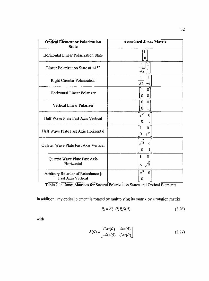
32
Optical Element or Polarization State
Associated Jones Matrix
Horizontal Linear Polarization State fl
[o
Linear Polarization State at +45° 1 ' \
_1_
Right Circular Polarization 1 1 '
-i
Horizontal Linear Polarizer "l 0"
0 0
Vertical Linear Polarizer "0 0"
_0 1_
Half Wave Plate Fast Axis Vertical 'e" O'
. 0 1.
Half Wave Plate Fast Axis Horizontal "1 0"
_0 e'\
Quarter Wave Plate Fast Axis Vertical
.Jt
0
0 1
Quarter Wave Plate Fast Axis Horizontal
"1 0 .n
0
Arbitrary Retarder of Retardance (|) Fast Axis Vertical
1 \
O
1 1
Table 2-1: Jones Matrices for Several Polarization States and Optical Elements
In addition, any optical element is rotated by multiplying its matrix by a rotation matrix
P,=Si-e)P,S{e) (2.26)
with
S{d) = Cos{G) Sin{6)
-Sin{0) Cos(6) (2.27)

33
For the very general case of an arbitrary retarder of retardance (|) at an angle 0, the
associated Jones matrix is
Re = Cos{-d) Sin{-d)'
-Sin{-G) Cos{-e)
e" 0
0 1
CosiO) Sin{d)'
-Sin(0) CosiG)
(2.28)
e''^Cos\e) + Sin\e) e'*Cos{G)Sin{e)-Sin{e)Cos{e)
e'^Cos{e)Sin{d) - Sin{e)Cos{e) e'^Sin" {6) + Cos^ {6)
with 0 measured from the horizontal axis.

34
CONVENTIONAL PDI
The conventional PDI is a simple common-path interferometer capable of directly
measuring optical wavefronts for metrology and optical testing. The PDI's primary
advantage is its common-path design, where the test and reference beams travel the same
or almost the same path. This design makes the PDI extremely useful where
environmental isolation is not possible or the reduction in the number of precision optics
is required. This chapter discusses the operation of the conventional PDI both
qualitatively and through scalar diffi"action theory.
QUALITATIVE DESCRIPTION OF THE CONVENTIONAL PDI
The PDI is a simple two-beam interferometer where the reference beam is created from a
portion of the test beam by diffi"action via a small pinhole in a semitransparent coating.
The operation of the PDI is shown in Figure 3-1.
Test Lens PDI Plate Spatial
Filter
CCD Camera Laser
imaging Lens
Fig 3-1. Conventional PDI
Light from the laser is sent into a spatial filter whose pinhole acts as a point source for the
test lens. In the above diagram, the spatial filter pinhole is positioned at twice the front
focal distance from the test lens, producing a focus spot at twice the back focal distance
of the test lens. The experimental setup could be modified such that collimated light is

35
incident on the test lens producing a focus spot at the back focal distance of the test lens.
The spatial filter pinhole is chosen sufficiently small so that the size of the focus spot
formed by the test lens is solely due to the diffraction limit of the test lens plus
aberrations. The PDI plate, which is created by placing a small pinhole in a
semitransparent coating, is placed at the focus spot of the test lens. The diameter of the
pinhole created is approximately half the unaberrated Airy disk diameter of the test lens
(Wyant 1979), or
This requirement sets the lower limit on the f-number of a particular optic that can be
tested for a given pinhole diameter. A 5|im diameter pinhole can be used to test optics
with working f-numbers of 6.5 and larger. The pinhole is aligned so that it is coincident
with a portion, usually the center, of the focus spot formed by the test lens. The portion
of light incident on the pinhole is diffracted by the aperture into a spherical wavefront
that serves as the reference wavefront for the interferometer. The diameter constraint of
the pinhole produces a reference wavefront with only minimal amplitude and phase
variations (Wyant 1979). The remainder of the light from the test lens is attenuated but is
otherwise transmitted unaffected through the semitransparent region surrounding the
pinhole shown in Figure 3-2. With the PDI pinhole smaller than the Airy disk radius of
the test lens, the angular subtense of the diffracted reference beam will always be larger
than the angular subtense of the test beam ensuring the entire optic is tested.
# working^ pinhole (3.1)

36
Aberrated Clear Test Wavefront hocus bpot Kinnoie
c: Test Wavetront
Semitransparent v^e^.eUont Region
Figure 3-2: Operation of the PDI Plate
The test and reference wavefronts pass through the imaging optics, which form an image
of the test lens superimposed with interference fringes on the CCD camera. For good
fiinge contrast, the test beam is carefully attenuated so that the relative intensities of the
test and reference beams are similar. Typical transmittances of the PDI plate are .01 to .1
(Steel 1983).
SCALAR DIFFRACTION THEORY REPRESENTATION
A theoretical model of the conventional PDI is derived from scalar diffraction theory.
This model serves as a starting point for describing the PPSPDI presented later, and
shows the origin of both the test and reference beams incident on the image plane;
however the effect of lateral misalignment of the PDI pinhole is not presented. The PDI
schematic in Figure 3-3 indicates the planes used in the analysis.

37
xi.yi X2.y2 X3,y3
PDI Plate Imaging Lens
Test Lens
CCD Camera
U(xi,yi) U(X3,y3) tPDl(X2,y2)
U(x2,y2)
Fig. 3-3: Schematic of the PDI for scalar diffraction model
For this scalar diffraction model to be valid, four assumptions are made (Goodman 1996)
1. Assume the geometric lens law, — + — = —, for the test optic is satisfied. s s' f
2. Neglect petzval curvature across the image plane
3. Neglect complex proportionality constants.
4. Place the PDI pinhole coincident with the center of the test optic focus spot.
The optical field just behind the test lens is described by the lens pupil fiinction
U(,x^,y,) = cyl{: )e .ikfixi.n) (3.2)
where di is the diameter of the lens and W(x^,y^) is the aberration function for the test
/ 2 ^ lens. The cylinder function, cyl(^——)> represents a function equal to zero
d,
V I 2 ;it:, +3;, < di/2, where the function equals one (Gaskill, 1978).

38
In propagating to the test lens focus and neglecting petzval curvature at the focus plane,
the impulse response of the test lens
1 fr -i^U\X2-yiy2) ^(^2.^2) = 71 \\U{x^,yx)e dx^dy, (3.3)
with zi and Z2 equal to the object and image distances for the test lens, simply Fourier
transforms the lens pupil function (Goodman 1996). The optical field just prior to the PDI
plate is represented by the Fourier transform of the test lens pupil function
U-{x„y,) = (3.4)
The optical field is then multiplied by the transmittance function of the PDI plate given
by
IX2_^y^
d. ^PDI plate^plate)0'K , ) (3-5)
'2
with equal to the transmittance of the semitransparent coating and c/j equal to the
diameter of the pinhole, resulting in
^ (^2 ' 3^2 ) ~ ^PDI ' ^ (.^2 ' y2 )
(3.6)
Finally the imaging lens images the plane of the test lens onto the camera. The final
image is a scaled and possibly magnified copy of the wavefi"ont at the test lens, modified
by the PDI plate and convolved with the impulse response of the imaging lens. In the
limit that the imaging lens diameter is very large, the impulse response becomes a delta

39
function that samples but does not smooth the incoming wavefront. The imaging lens has
the effect of Fourier transforming the field just after the PDI plate, U^{x2,y2)-
Neglecting petzval curvature across the image and a complex proportionality constant,
the field in the image plane is
U{x„y,) = **FT{U-{x„y,)} (3.7)
U { x ^ , y ^ ) = T p j „ * * U { x ^ , y ^ )
where Tpoi is the Fourier Transform of the of the transmittance fimction of the PDI plate.
So the field at the camera is the optical field just behind the test lens convolved with the
Fourier transform of the transmittance function of the PDI plate. Multiplied out this
becomes
n—r n—r
4 Azj a,
J x ^ + y ^ T T J X ^ + / ;rJx^ + y^ where Somb(— ) = )/ {— ), d is a constant and Ji(x) is a
d d i d
first order Bessel function. This equation shows that the interferogram is formed by the
coherent addition of an attenuated, aberrated test wavefi-ont and a reference wavefront
created by the convolution of the aberrated wavefi"ont with the Fourier transform of the
pinhole in the PDI plate. The test and reference beams are given by the first and second
terms in the above equation respectively. The test beam is an attenuated copy of the
original test lens pupil function while the reference beam is a significantly smoothed

40
version of the same test lens pupil function. The intensity is the true quantity measured at
the camera, so at the final image plane, the intensity is
which is simply the square modulus of the electric field at the camera.
In the limit that the PDI pinhole diameter approaches zero, the sombrero function is
approximated by a constant while the reference wave becomes a smooth, continuous
function. For relatively slowly varying aberration functions W(x^,y^) the reference
wave becomes spherical (Mercer, 1996).
(3.9)

41
POLARIZATION PHASE-SHIFTING POINT-DIFFRACTION INTERFEROMETER
The Polarization Phase-Shifting Point-Diffraction Interferometer (PPSPDI) is a
modification of the conventional PDI utilizing polarization changes in the incident beam
to induce a phase-shift. The PPSPDI retains the common-path design and advantages of
the conventional PDI while the novel PDI filter allows for phase shifting and increased
accuracy in phase measurement. The difference in the design lies in the construction of
the PDI filter. In the conventional PDI, the filter is a partially transmitting pinhole plate,
but the PDI filter in the PPSPDI is a pinhole etched into a thin film half-wave plate. This
chapter discusses the operation of the PPSPDI qualitatively, and through both scalar
diffraction theory and Jones calculus.
QUALITATIVE DESCRIPTION OF PPSPDI
The laboratory experiment is illustrated in Fig. 4-1.
Test Lens
Optics
Rotating Ground I \ Glass Plate
Analyzef^-*i. Imaging Optics
Imaging Optics
Polarizer EDM (0«) m
HWP (22.50) Spatial Filter
Source Reference
s
Fig 4-1: Operation of the PPSPDI
Light fi"om the laser operating at A,=632.8nm passes through the combination of a
polarizer and half-wave plate. The polarizer oriented at 0° is used to isolate a single,

42
linear polarization state while the half-wave plate at 22.5° rotates the polarization state so
its output is linearly polarized at 45°. The polarizer and half-wave plate combination
ensures selection of linear polarization at any desired angle by a rotation of the half-wave
plate. Following this combination is an electrooptic modulator with electrodes oriented
vertically (0°), that is used as the phase-shifter for the interferometer. When a voltage is
applied to the modulator, the index ellipsoid of the crystal inside the modulator rotates
producing a change in the index of refraction of the crystal in the plane perpendicular to
the electrodes. The linear input state at 45° is propagated through the modulator by
decomposing it into its orthogonal horizontal and vertical states, p and s, which
correspond to the eigenmodes of the modulator, hi propagating through the crystal, the
two orthogonal states will encounter a constant natural phase difference without an
applied field due to the nature of the crystal and an electrically induced phase difference
that increases linearly with the applied field. Because of these two facts, the horizontal
component, p, encounters a larger optical path through the crystal and is given an extra
phase, 6 that is changed by varying the field applied to the modulator shown in Figure 4-
1. Recombining the orthogonal components, the output of the modulator is in general
elliptically polarized. Following the modulator is a spatial filter with a 5)am pinhole. The
spatial filter acts as a point source and is positioned at twice the focal distance in fi"ont of
the test lens to simulate a 4-f imaging system with a magnification of -1. The spatial
filter pinhole is small so that the size of the focus spot formed by the test lens is due
solely to the diffraction limit of the lens plus aberrations. The test lens forms an
aberrated focus spot on the PDI plate, located at twice the focal distance behind the test
43
lens. The pinhole plate is constructed by etching the pinhole through a birefringent
silicon thin film half-wave plate with the fast axis oriented at 45° to the orthogonal
components of the incident beam, s and p. As with the conventional PDI, the diameter of
the pinhole created is approximately half the unaberrated Airy disk diameter of the test
lens (Wyant 1979), or
where the working f-number of the test lens in a 4-f imaging system is twice the actual
lens f-number. Again, the clear pinhole is aligned so it is coincident with the center of
the focus spot formed by the test lens. The portion of light incident on the pinhole does
not encounter the thin film half-wave plate and is diffracted into a spherical reference
wavefront retaining the elliptical polarization state of the incident beam. The thin film
half-wave plate transmits and attenuates the remainder of the light from the test lens,
rotates the s and p orthogonal states by 90°, and the s and p states emerge orthogonal but
flipped in orientation shown in Figure 4-2. This wavefr-ont retains the aberrations of the
incident wavefi"ont and serves as the test wavefi"ont for the interferometer.
# working, pinhole
(4.1)

44
Test Wavefront Aberrated
Focus Spot Clear
Pinhole
Test Wavefront
Half-Wave Plate Semitransparent
Region
Reference Wavefront
s
p(+5)
Fig 4-2: Operation of the PPSPDI Plate
An analyzer with transmission axis horizontal placed after the PDI plate isolates one set
of the orthogonal components fi-om the test and reference beams. Moreover, the analyzer
produces two interfering wavefronts, the test and reference wavefronts, with a variable
phase difference between them. By varying the voltage in the electrooptic modulator, the
phase difference between the test and reference wavefronts is varied causing phase
shifting. Both wavefronts then pass through imaging optics which image the plane of test
lens onto a rotating ground glass plate. Interference fringes are superimposed on the
image of the test lens on the rotating plate. The rotating ground glass plate reduces the
coherence of the system; thereby reducing the spurious fringes from the protective glass
plate in front of the CCD chip in the camera. The camera optics then image the
interference pattern produced on the ground glass plate onto the CCD.

45
OPERATION OF THE HALF-WAVE PLATE
The most important component in the PPSPDI is the thin film half-wave plate used to
create the pinhole filter; however its operation shown in Figure 4-3 is not completely
obvious.
SA y \ \ \
X
FA SA FA SA FA
/
/
/
/ /
/ /
/ /
/ /
/ /
\ \ \ \ \
/ /
E,
SA y FA SA FA SA
/ 1
/ /
/ / /
/ /
^ to / \ '
/ \ / \
/ \ / \
/ /
/
\ \ \
\
/ /
/ /
/ /
/ /
/ /
\ \ \ i \ \
N /
/ '
/ \ / \
/ \ / \
/ \
Orthogonal state incident on HWP
Splitting of state along fast and slow
axes
180° phase lag along slow axis
Recombination upon exiting HWP
Fig 4-3: Operation of the Thin Film Half-Wave Plate
The elliptically polarized Ught incident on the thin film is decomposed into horizontal
and vertical orthogonal components, Ex and Ey, and the fast axis of the film is oriented at
45°. As the light is incident on the thin film, each of the two components is decomposed
into the two eigenmodes of the film along the fast and slow axes.
~ xFA ^xSA
~ ^yFA ^ySA
(4.2)
where subscript FA denotes the fast axis and SA the slow axis, hi propagating through
the film, the components along the slow axis encounter a 180° or e'" phase lag relative to
the fast axis.

46
~ ^xFA "*• xSA^ ~ xFA ^xSA
~ yFA ^ySA^ ~ yFA ~ ySA (4.3)
Upon exiting the half-wave plate thin film, the components along the fast and slow axes
are recombined. From Fig 4-3, it is observed that
The incident horizontal and vertical orthogonal components are rotated by 90° in passing
through the half-wave plate thin film.
The effect of the rotation of the orthogonal horizontal and vertical components upon
passing through the half-wave thin film becomes important when observing both the test
and reference beams in the interferometer. Assuming that the electrooptic modulator
adds additional phase to the horizontal component, the reference beam retains the phase
shift on the horizontal component. On the other hand, the test beam passes through the
thin film half-wave plate, which both rotates its polarization state by 90° and causes the
phase shift to be on the vertical component. This allows isolation of either the horizontal
or vertical components of the two beams and production of phase shifting interferograms.
SCALAR DIFFRACTION THEORY REPRESENTATION
A theoretical model of the PPSPDI is derived fi"om scalar diffi"action theory in a similar
manner to the conventional PDI in the previous chapter. This model shows the origin of
both the test and reference beams as well as the origin of the phase shift; however.
^x Final ^y Initial
F — F y Final x Initial 'x Initial
(4.4)

47
misalignment of the PDI pinhole is again not presented. The PPSPDI schematic in
Figure 4-4 indicates the planes used in the analysis.
xi.yi X2.y2
Half-Wave PDI Plate
Imaging Lens
X3,y3
Rotating Ground Glass Plate
Test Lens
U(xi,yi) U(x3,y3) tPDl(X2,y2)
U(x2,y2)
Fig. 4-4: Schematic of PPSPDI for Scalar Diffraction Model
For the scalar diffraction model to be valid, four assumptions are made (Goodman 1996)
1. Assume the geometric lens law, —+— = —, for the test optic is satisfied. s s' f
2. Neglect Petzval curvature across the image plane.
3. Neglect complex proportionality constants.
4. Place the PDI pinhole coincident with the center of the test optic focus spot.
In this model, the horizontal and vertical orthogonal components of the input polarization
state are traced separately through the optical system. The electrooptic modulator
produces a variable e"'additional phase in one of the components that this model
assumes is the horizontal component, Ex. The optical field just behind the test lens for
both polarization states is described by the lens pupil function

48
UM.y,) =
(4.5) / 2 . 2
rV^i + >*1 (^1. Ji) = EyCylir^!—- )e'
«!
where di is the diameter of the test lens and W{xi,y^) is the aberration function for the
I 2 , 2 •JX-. +>*, test lens. The cylmder function, cyl(- ), represents a function equal to zero
d,
everywhere except for < di/2 where the function equals one (Gaskill 1978). In
propagating to the test lens focus and neglecting Petzval curvature at the focus plane, the
impulse response of the test lens Fourier transforms the lens pupil function for each of the
orthogonal components (Goodman 1996). The optical field just prior to the PDI plate is
represented by the Fourier transform of the test lens pupil function
' (4.6) / 2 . 2
u; ( x „ y , ) = S { E , c y l C"'
The optical field is then multiphed by the transmittance function of the PDI plate given
by
/ 2 2
'^PDUx ~ Opiate,FA •*" ^plateM^ (1 ~ plate,x)
' (4.7) x^ + ^
' ^ P D I , y ~ p l a t e , F A ^ p l a t e + ( 1 ~ p l a t e , y ) 0 ' ^ ( ) Cti

49
where di is the diameter of the pinhole and is the transmittance of the film for light
polarized in the specified direction. The fast and slow axes of the thin film half-wave
plate used to create the pinhole filter are oriented at 45° to the x and y orthogonal
components. In propagation through the PDI filter, the horizontal and vertical
polarization states must be fiirther decomposed into components along the fast and slow
axes. After propagating through the film, the individual components along the fast and
slow axes are recombined. In propagating through the PDI plate, the optical field
becomes
The net result of the thin film half-wave plate is a rotation of the orthogonal components
by 90° giving a final result for the optical field after propagating through the PDI plate of
(4.8)

50
r~2. 2
+ (1 c?,
U;(x„y,) =
(4.9)
I ~. I 2~ 2 „ , , ,V5+Z. + (1 -l^,y)cylC"'J " mE^cylC"' V"'"'!
An analyzer with transmission axis either horizontal or vertical placed after the PDI plate
isolates one set of orthogonal components exiting the PDI plate, hnaging optics then
image the plane of the test lens onto a rotating ground glass plate. The image on the
ground glass plate is a scaled and possibly magnified copy of the wavefront at the test
lens, modified by the PDI plate and analyzer and then convolved with the impulse
response of the imaging lens. In the limit that the imaging lens diameter is very large, the
impulse response becomes essentially a delta function that samples but does not smooth
the incoming wavefront. The imaging lens has the effect of Fourier transforming the
field just after the PDI plate and analyzer combination. Neglecting Petzval curvature
across the image and a complex proportionally constant, the field at the ground glass
plate is
PDI+Analyzer **FT{U-{x„y,)}
~ PDI+Analyzer
where Tpoi is the Fourier transform of the transmittance function of the PDI plate and the
effect of the transmittance function of the analyzer is to allow transmission of only one

51
orthogonal component of the field. Assuming that the analyzer allows transmission of
only the horizontally polarized component, the field at the rotating ground glass plate is
is a first order Bessel function. This equation shows that the interferogram is formed by
the coherent addition of an attenuated aberrated test wavefront and a reference wavefi"ont
formed by the convolution of the aberrated wavefront with the Fourier transform of the
pinhole in the PDI plate. The test and reference beams are the first and second terms in
the above equation respectively with the variable phase shift term in the reference
beam. The test beam is an attenuated copy of the original test lens pupil function while
the reference beam is a significantly smoothed version of the same test lens pupil
function. The CCD camera images the interferogram produced at the rotating ground
glass plate. Since intensity is the true quantity measured by the camera, the intensity at
the ground glass plate is
(4.11)
+ (1 -1 plate..) Sombi-^ ) * *cyl 4 Az. a,
where Somb{ ) where d is a constant and Ji(x)
(4.12)
which is the square modulus of the field at the ground glass plate.

52
As before, in the Umit that the PDI pinhole diameter approaches zero, the sombrero
function is approximated by a constant, and the reference wave becomes a smooth,
continuous function. For relatively slowly varying functions W(x^,yj) the reference
wave becomes spherical (Mercer 1996). The effect of pinhole errors is presented in a
later chapter.
JONES MATRIX REPRESENTATION
One can model the PPSPDI using Jones matrices. For completely polarized systems such
as the PPSPDI, the system elements are represented by 2x2 matrices with the incident
field represented by a 2x1 matrix. Propagation of the beams is accomplished by
multiplying the incident field by the matrix for each element in the system as shown
below
Output
E Output = \j^inal Element'^...^'^ Element~^^' Element^
E^ Input
E Input (4.13)
The Jones matrices necessary to simulate the PPSPDI are given in table 4-1.

53
Optical Element or Polarization State Jones Matrix
Linear Polarization State at +45° 1 rr
V2L1.
Horizontal Linear Polarizer "1 0"
0 0
Vertical Linear Polarizer
1 1
0 0
0
1 1
Half Wave Plate Fast Axis Vertical 'e" 0"
. 0 1.
Rotation Matrix Cos{0) Sin{6)
-Sin{0) Cos{0)
Arbitrary Retarder of Retardance (j) Fast Axis Vertical 1
i
0
1 t
Test Surface 0
0
Electrooptic Modulator with Retardance On the Vertical Component
"1 0 •
_0
Table 4-1: Jones Matrices for Modeling the PPSPDI
For the Jones matrix model to be valid, the test and reference beams must propagate
through the system separately. Both the test and reference beams begin as a single
linearly polarized beam at 45° passing through the electrooptic modulator that adds a
temporal phase to the vertical orthogonal component.
Test = -^ V2
Reference = •
1 0
0 e''
1 "1 0 • "1"
1
0 1
1
(4.14)

54
The beams then pass through the test optic, which adds a spatial phase. A, to both
components. The spatial phase added to the test and reference beams is directly related to
the optical path difference or surface error on the test optic. The test and reference beams
are represented by
Test = -7=
V2
0 ' " 1 0 " T
_ 0 _ 0 _i_
Reference = 1 0" "1 0" "1"
0 _o 1
(4.15)
Both beams are then focused onto the PDI plate. The test beam passes through the half
wave plate thin film while the reference beam passes through the pinhole. The reference
beam in passing through the pinhole loses the spatial phase associated with the test optic
but retains the temporal phase fi-om the electrooptic modulator. So, only the test beam is
multiplied by the matrix associated with the half wave plate while the reference beam
loses the matrix associated with the test optic.
1 Test = "0 f 0 ' "1 0' "1"
1 0_ 0 1
0 I
_i
Reference = 1 "1 0"
1
0 1
1
(4.16)
Finally, both the test and reference beams pass through an analyzer with its transmission
axis either horizontal or vertical. If the transmission axis is assumed to be horizontal, the
test and reference beams become

55
Test = • 1 "1 0" "0 r •g''" 0 ' "1 0" "r
1 o
o 1 1 0 0 1 _i_
Reference = "1 0" "1 0 • T
0 0 1
o _l_
(4.17)
Multiplied out the test and reference beams become
Test = ^= V2
Reference =
J(S+^)
(4.18)
The total amplitude in the interferogram is simply the addition of the test and reference
beams.
Total Amplitude = 0
(4.19)
The total intensity in the interferogram measured at the camera is the square modulus of
the amplitude
Total Intensity = 1 + Cos{d + A) (4.20)
where A is the phase associated with the optical path difference in the test optic and 6 is
the variable phase shift from the electrooptic modulator. The phase from the test optic, A,
is ideally determined by phase shifting the above intensity and entering the values into a
phase shifting algorithm. Using a four step algorithm

56
/, =1 + CO5(A)
=\-SH^)
/j =1-CO5(A)
<5 = 0
2 5 = n
(4.21)
/^ = 1 + Sin{A) „ 3 71 o =
2
Phase = ArcTan——— /,-A
- ArcTan l + 5w(A)-(l-5m(A))
(4.22) 1 + CO5(A)-(1-CO5(A))
= ArcTan{Tan(Ay)
= A
So, by varying the phase produced by the electrooptic modulator, the surface phase of the
test optic is determined from the resulting interferograms as expected.

57
BIREFRINGENT THIN FILMS AND PINHOLE CONSTRUCTION
The most important component in the PPSPDI is the novel pinhole filter that is
constructed by etching a pinhole into a half-wave plate birefringent thin film. This
chapter begins by discussing the deposition and properties of the novel birefnngent thin
films. The second half of the chapter covers techniques used to etch the films and the
successes or failures of each.
BIREFRINGENT THIN FILM DEPOSITION AND PROPERTIES
The pinhole filter in the PPSPDI is created fi-om a birefiingent silicon thin film with a
biaxial index structure. The locations of the three orthogonal principle dielectric axes and
associated indices of refraction are fixed by the deposition geometry and symmetry.
Birefringent thin films are deposited in much the same way as isotropic films. In
isotropic films, the evaporant material is heated in a vacuum with either an electron beam
gun or heated coil, and the evaporant atoms travel from the source to the substrate where
they condense. The subsfrate, oriented at an angle 0 to the evaporation source, is
stationary and the film grows with a tilted columnar microstructure as shown in Figure 5-
1. Limited mobility of the evaporant atoms along with self-shadowing cause the
columnar structure growth. The condensing atoms are unable to move far enough to fill
vacant positions in the shadow of existing material (Hodgkinson 1997).

58
i I G l i O I 8 9 G a ( p r o g r a m d a t e 2 3 S e p t e m b e r 1 9 8 9 ]
I R U N I D : A S 0 5 - 6 t - 0 6 4 D i T E : 2 0 S e p t e n i e r 1 9 8 9
I S u r f a c e K o b i l i t j , I n y i ! = 6 4 ; J , 0 . 1 , = 6 0 ( i e | .
7 5 0 i 3 0 0 ( S O O i Z O O d i a n t ) ; D l / B s = 0 , 9 0
Fig 5-1: Characteristic Tilted Columnar Structure of Thin Films Deposited at Oblique Licidence (Hodgkinson 1997)
In the case of the birefringent films, the substrate is not stationary during the deposition
process. Evaporant atoms condense on the substrate shown in Figure 5-2, but after every
few nanometers of deposition, the substrate is rotated by 180 degrees. A crystal sensor in
the chamber monitors the deposition thickness to ensure proper rotation of the substrate.
In-situ optical measurements of the films can be taken through windows in the vacuum
chamber.

59
Crystal
Anisotropy
Substrate
Temperature
Ion Gun
Evaporation Controller
Pressure Thermal Evaporator E-beam
Gun —I Oxygen
Fig. 5-2: Deposition Apparatus for Birefringent Films
Rotating the substrate causes the columnar microstructure to grow normal to the substrate
illustrated in Figure 5-3.
Fig 5-3: Characteristic Normal Columnar Structure For Bi-Directional Deposited Birefringent Films (Hodgkinson 1997)

60
The material used for the films is silicon that is not birefiingent in typical oblique
deposition. The birefiingence in the thin films is caused by the normal columnar
microstructure. This birefiingence due to the structure of the film as opposed to the
material itself is termed form birefiingence. For form birefiingence, the columns are
much thicker or bxmched preferentially in the direction perpendicular to the deposition
plane, and typically both effects are present. This form birefiingence depends on both the
column shape and packing density of the columns to cause direction-related variations in
the refractive index. This deposition geometry causing the columnar structure to grow
normal to the substrate, sets the orientations of the three principle dielectric axes: normal
to the substrate, perpendicular to the deposition plane, and parallel to the deposition plane
(Hodgkinson 1997). The direction perpendicular to the deposition plane, which has a
greater packing density of colimins, has a large index of refraction, ne, and is considered
the slow axis for the retarder. The direction parallel to the deposition plane has a lower
index of refraction, no, and is the fast axis for the retarder. The relationship describing
the retardance of the film in waves for a given wavelength X is
where the thickness of the film, t, determines the retardance. For a half-wave plate this
gives a film thickness of
t t (5.1)
X (5.2) t =
2tm

61
The index difference, An, is not constant with wavelength and is given by a dispersion
equation unique for each film material. An is a function of wavelength and for the silicon
films is
An,=An„,(l + c(^-^)) (5.3)
where c was experimentally determined as -268332 and Aness is .2816 (Hodgkinson
2001). This gives a characteristic dispersion curve that increases with wavelength given
in Figure 5-4.
An
0.4
0.35
0.3
0.25
600 700 800 900 1000
Fig 5-4: Dispersion Relation For Silicon Birefnngent Thin Films
Consequently, one may determine the index difference between the fast and slow axes for
any wavelength and thus the total retardance at any wavelength for any known film
thickness. Now, one may achieve the desired retardance by depositing a film of a
specific, required thickness.

62
The retardance of the wave plate is monitored in-situ as the film is deposited using
perpendicular incidence ellipsometry (Hodgkinson 1997). This was the method used
when the half-wave films for the PPSPDI were deposited. The light beam is circularly
polarized when it reaches the film shown in Figure 5-5. After passing through the
sample, the beam encounters a rotating polarizer and a spectral bandpass filter before
being detected by a photomultiplier. The signal detected at the photomultiplier oscillates
as a function of two variables: the angle between the axis of the rotating polarizer and
the p polarized portion of the light leaving the sample, and the total phase retardance of
the film including interference, A. From this signal, A is determined while the film is
deposited. Once the correct total phase difference is reached, deposition is stopped.
Filament Source
Crystal Monitor
Linear Input
Rotating Bandpass Polarizer Filter PMT
Circular Polarizer
E-beam Source
Substrates
Fig 5-5: Perpendicular Incidence Ellipsometry
In a similar manner, the principle refractive indices are measured using two ellipsometers
in transmission mode at different angles in the deposition plane as the film is deposited.
This is a significantly more difficult process, as the gradient of the smoothed retardation
versus thickness plot is necessary to eliminate the effects of interference (Hodgkinson
1998). Each ellipsometer provides phase retardation versus thickness information as the

63
film is being deposited, but at different angles. Two different angles are required to
allow two independent phase retardation versus thickness measurements to be taken.
The smoothed versions of these plots give differences in the indices of refi"action for the
different ellipsometer angles. With two independent values at two different angles, the
principle indices of refi-action parallel and perpendicular to the deposition plane are
determined. The modulation in the curves due to interference effects, removed for
determination of the first two indices, allows the determination of the third principle
index of refi*action perpendicular to the surface of the film. The inherent problem with
this measurement is that one must determine the angle of the columnar microstructures in
order to calculate the indices. The tangent rule
tan(4^) = tan(0) (5.4)
which approximates the angle of the column structures, T, based on the deposition angle,
0, is often unreliable for biaxial films so one must determine the actual angle using an
SEM after deposition is completed. Having to determine the column angle after
deposition defeats the purpose of the in-situ measurement.
ARGON ION MILLING
The first method used to etch the pinhole in the films was argon ion milling that uses a
photolithographic process to etch features into the film illustrated in Figure 5-6.

1)
64
Substrate with HWP Film
Spin-Coat with Photoresist
3) 4)
Expose Pinhole Pattern into Photoresist
Develop Photoresist
6)
Ion Mill Film Remove Photoresist
Fig 5-6: Photolithographic Process for Argon Ion Milling
The process begins by spin coating the thin film with a layer of Shipley 1813 photoresist.
The thin film is coated by spinning the sample at SOOrpm for 5 seconds and then SOOOrpm
for 30 seconds yielding a uniform photoresist coating. The thickness of the coating is
unimportant as long as it can withstand the etching process. The photoresist coating is
baked for 3 minutes at 100°C in an oven to harden the photoresist. Using a mask aligner,
a chrome-on-glass contact mask is used to expose the pinhole pattern into the photoresist.
The sample is then submerged in developer for approximately 30 seconds that removes
the exposed photoresist creating the pinhole pattern in the unexposed photoresist. After
rinsing in deionized water to remove the developer, the photoresist is again baked in an
oven at 100°C for 5 minutes to harden the photoresist and remove any remaining water
before the etching process. This remaining photoresist serves as a shield for the film
under it during the etching process.

In an argon ion mill, the sample with phororesist mask is placed on the cathode of the
system inside a vacuum chamber pictured in Figure 5-7. The anode of the system
consists of an argon ion gun and a high voltage bias grid that provides additional
acceleration to the ions. Argon ions are produced by the ion gun and initially accelerated
by the bias grid. Upon leaving the anode the ions are further accelerated due to the bias
applied between the anode and cathode. The ions travel to the cathode and strike the
sample with very high momentum causing atoms of the sample to dislodge. This
bombardment of the sample with high velocity argon ions is the physical etch process
used to create the pinhole features. Because of the highly directional nature of the ions in
the electric field, the etch is also highly directional leading to very accurate feature
profiles (Hakola 2003). The photoresist mask must withstand more ion bombardment
than the thin film for the etch process to work correctly. Only the portion of the film not
protected by the photoresist is etched by the argon ions, the remaining film is left
unaffected. Once the film is etched, the remaining photoresist is removed by rinsing the
sample with acetone leaving the bare film with etched features.

66
Cathode
Sample
Vacuum Chamber Anode
Ar* Ion Gun
RF- Generator
Biased Grid
Fig 5-7: Argon Ion Mill
The biggest problem in using argon ion milling is heat. As the ions are accelerated, they
become very hot. Consequently, as the ions strike the sample, not only do they etch the
surface but heat it as well. Table 5-1 lists the minimum etching parameters for proper ion
mill to operation. In turn, these parameters are used to minimize the heating of the
sample. Even with the minimimi energy, this heating of the sample caused the
photoresist to bum long before the film etched, therefore, argon ion milling is not a viable
option for etching the pinhole.

67
Parameter Value RF Power 250 W
Beam Current 160 mA Beam Voltage 250 V
Acceleration Voltage 300V Neutralization Current 175 mA
Etch Source Gas 10.0 seem FBNl Gas 5.0 seem
Chamber Gas 0.0 seem Arm Angle 0.0 deg
Platen Rotation Speed 20.0 rpm Table 5-1: Argon Ion Mill Parameters
REACTIVE ION BEAM ETCHING
The second etching method attempted was reactive ion beam etching. Unlike argon ion
milling, this process is both chemical and physical. The etchant is chosen such that its
chemical reaction with the sample surface produces a volatile species. The etchant
strikes the sample, chemically reacts with the surface and by forming a volatile
compound removes a small portion of the surface of the sample.
Reactive ion beam etching follows a very similar process to argon ion milling in the
preparation of the sample. A layer of photoresist is spun onto the film and the pinhole
pattern is created in the photoresist using the same contact mask photolithographic
process.

68
Electrode
Ionized Plasma
Etchant (free radical) Creation
Etchant Transfer
Byproduct Removal
Etchant Absorption Etchant/Fllm
Reaction Film
Electrode
Fig 5-8: Reactive Ion Beam Etch Process
Once the mask is patterned onto the sample, the sample is placed on one of the electrodes
of the reactive ion etcher shown in Figure 5-8. Next, the chamber is pumped to form a
vacuum and a small concentration of etchant gas is inserted into the system. For the
silicon films, the etchant was chosen to be tetrafluromethane, CF4. As an electric field is
applied across the electrodes, a plasma is formed as electrons ejected fi"om the negative
electrode start the process of breaking the tetrafluromethane into fi*ee radicals
e'+CF^ ^CFj+F + e (5.5)
A voltage bias develops between the plasma formed by the fi^ee radicals and the
electrodes causing the free radicals to move toward the electrode with the film to be

69
etched. Striking the film, the fluorine radicals react with the silicon producing the
volatile compound
Si + 4F->SiF4 (5.6)
that comes off the surface removing a molecule of silicon (Akinwande 2003). The
surface is etched essentially molecule by molecule. Since tetrafluromethane was chosen
to etch silicon specifically, the photoresist is left untouched, accordingly, only the film
not protected by the photoresist mask is etched. Once the etching is completed the
photoresist is removed by washing the sample in acetone leaving only the film with the
pinhole etched in it.
Reactive ion beam etching using tetrafluromethane will etch the silicon films but not with
the required feature profiles. Because the process is chemical as well as physical, etching
occurs fast in all directions. The etching process tends to undercut the mask leaving a
sloping sidewall to the feature instead of a vertical feature profile. Because of the
undercutting of the mask, reactive ion beam etching will not produce features with walls
vertical enough for optimal operation of the PPSPDI. Figure 5-9 gives the profile of the
features produced during a partial etch that have walls with an angle of about 60 degrees
from vertical. With a full etch depth of 1 micron, the walls have an angle of about 45
degrees. The profile in the figure was taken using a WYKO NT2000 interference
microscope on a sample that was etched with tetrafluromethane for 70 minutes. This
angled profile will produce a pinhole with a tapered bore, that will introduce wavefi-ont
errors of more than .01 waves into the reference beam for only a 20 degree taper when

70
used in a PDI (Goldberg 1996). Because of the angled profile, reactive ion beam etching
is not a viable option for etching the pinholes for the PPSPDI.
Y Profile X 0 8 um
um W
Ojjj-I zzl X: 40,4 um t -1 [ Y.-0.:»8um j
010-
4ijQ(h
-010-
-050-
•0.» •"T—T~
10 20 90
X41.2um Y; 0,218 um
•>1 OD c 3
so flO •0 «0
Fig 5-9: Edge Profile of Reactive Ion Beam Etched Thin Film
FOCUSED ION BEAM ETCHING
Focused ion beam etching was the third method used to etch the pinhole in the silicon
thin film. A focused ion beam etcher operates similar to a scanning electron microscope
since both instruments take charged particles fi-om a source, focus them into a beam, and
then scan across small areas of a sample. A focused ion beam etcher differs from an
electron microscope by using gallium ions to form its beam, instead of electrons. Since
galliimi ions are orders of magnitude more massive than electrons, a FIBE's ion beam
mills the sample surface instead of imaging it (Street 2002). This etching method
provides a way for a maskless and resistless pinhole etch process.

71
The FIBE uses a very sharp tungsten needle wetted with gallium. The tip of the needle is
subjected to a high voltage causing the ejection of gallium ions and acceleration toward
the sample. The gallium ions are focused by electromagnetic fields into a highly focused
beam and steered to a specific spot on the sample (Freidrich 2002). The kinetic energy of
the ions as they strike the sample causes the ejection of atoms fi^om the sample through a
sputtering process illustrated in Figure 5-10. A wide variety of shapes are possible by
varying the scan rate, pattern and energy of the ion beam as well as the dwell time of the
beam at any given spot.
Ion Source
Ga'^ Ions
Ejected Sample ^ Atoms ^
Film
"W Etched Feature
Fig 5-10: Focused Ion Beam Etching
The focused ion beam etching of the silicon films was done by Integrated Reliability
Corporation of San Diego, California. Because the FIBE uses a highly focused beam of

72
ions, there is no need for the photoresist mask used in the previous two etch methods.
The desired etch pattern is programmed into the computer controlling the FIBE that
positions and scans the ion source to etch the features while leaving the remainder of the
film imtouched. The FEI FIB 200 system used has a lateral ion beam resolution of 12-
nm, that for a 5-micron pinhole gives a maximum etch error of .25%. It is possible to
etch the feature profile to within 3 degrees of vertical, a marked improvement over 45-
degree profile achieved with the RIBE method. An integrated high magnification
microscope was used to image the etched pinhole pictured in Figure 5-11.
Fig 5-11: Focused Ion Beam Etched Pinhole in Silicon Thin Film
Focused ion beam etching produces the best result of all etch methods attempted and is
the best choice as the process to create the pinholes for the PPSPDI. While requiring the
fewest steps to complete, it produced features with very high lateral resolution and near
vertical edge profiles.
73
ERROR ANALYSIS OF THE PPSPDI
In this chapter, mathematical models are developed to investigate the systematic errors in
the PPSPDI. Because the test and reference beams are separated by polarization state, the
PPSPDI is exceptionally sensitive to errors in the alignments and retardances of it various
polarization optics. The three most important of these are the retardance of the thin film
used to construct the pinhole filter, angle of the fast axis of the film, and the angle of the
final analyzer used to obtain the interference between the test and reference wavefironts.
In turn, these errors cause discrepancies in the phase shifts, intensity modulations
between phase steps and error in the final measured phase.
NONIDEAL JONES MATRIX PROPAGATION
In Chapter 4, the ideal Jones matrix representation for the PPSPDI was presented. This
model assumed that the film used to create the pinhole plate is a perfect half-wave plate
oriented at exactly 45° and the transmission axis of the final analyzer was precisely
horizontal. Unfortunately, this is not the case since not only is the thin film not a half-
wave plate, but the diattenuation of the film is nonzero. The film used in the PPSPDI
was measured on an Axometrics Muller Matrix Polarimeter and found to have a
retardance of 160° ± .5° and diattenuation of 20% + .5%. As a result of the diattenuation,
the film absorbs differently along the fast and slow axes in addition to the error in the
retardance. It is also expected that the alignment of the film will not be exactly 45° and
neither will the orientation of the transmission axis of the final analyzer be exactly

lA
horizontal. Consequently, it is imperative to develop a new Jones matrix model that takes
into account the possible error sources.
For new model validity, the test and reference beams must propagate through the system
separately just as in the ideal Jones matrix case. Both the test and reference beams begin
as a single linearly polarized beam at 45° passing through an electrooptic modulator that
adds a temporal phase to the vertical orthogonal component. The mathematical equations
are
Test = V2
1 0
0 e' iS
1 fl 0^ Reference = —pr
V2I0 e' iS
R A\ (6.1)
where 6 is the temporal phase shift introduced by the modulator and A is a beam balance
constant determined by the properties of the pinhole filter. Next, the beams pass through
the test optic, where a spatial phase. A, is added to both components. The spatial phase
added to the test and reference beams is directly related to the optical path difference or
surface error on the test optic. The test and reference beams are represented by
Test = 1
Reference= 1
1 0 "i
0 e iS vly
0 0 e' /A
1 (6.2)
0 e js
Other than the beam balance factor, the two beams are identical up to this point. After
the test optic, the beams are focused onto the PDI plate. The test beam passes through
the thin film retarder with retardance ^ and fast axis oriented at an angle 0 from vertical

75
while the reference beam passes through the pinhole. The diattenuation in the thin film is
20%, meaning the slow axis of the film transmits 80% of the light transmitted by the fast
axis. The reference beam in passing through the pinhole loses the spatial phase
associated with the test optic but retains the temporal phase fi"om the electrooptic
modulator. Accordingly, only the test beam is multiplied by the matrices associated with
the rotated thin film while the reference beam loses the matrix associated with the test
optic. This is the point where the beam balance factor, A, becomes important. A is
determined by the amount of light diffracted by the pinhole and absorption of the thin
film, and it measures how much light is diffracted by the pinhole into the reference beam
as opposed to transmitted by the film in the test beam. The closer the balance between
the beams, the closer this value approaches unity. Experimentally, the transmission of
the film along the fast axis is about 55%. For a moderately aberrated system, 25% of the
incident light is assumed incident on the pinhole, which is half the Airy disk size and
centered in the focus spot of the test optic. For these values, A was assigned a value of
.6; therefore, the Jones matrix representation of the beams after the pinhole plate is
Test Cos{-e) Sin{-d)
-Sini-0) Cos(-e)
^ .%e'* 0^
0 1
Cos{6) Sin{9)
-Sin{6) Cos{9)
f 'A 0
,0 e'%
1 0
0 d'
f<\
Rotation Matrix (-$) Retarder of Retardance ^ and .8 Diattenuation
Reference=4-V2
Rotation Matrix (d)
(6.3)
1 0
vO
^6^
Finally, the test and reference beams pass through an analyzer with transmission axis
oriented at an angle \\i from horizontal. This gives the final Jones matrix representation
of the test and reference beam amplitudes at the camera of

76
Test = 4~2
Cos{y/Y Cos{i^)Sin{i^)
Cos(i//)Sin(i//) Sin(ii/y
^ Cos(0) SiniO)^
-Sini0) Cos{0)
^^Cos(-e) 5m(-6')Y.8e'^ 0^
-Sin(-6) Cos(-6) 0 1
0
0 e"
1 0
0 e" (6.4)
Reference=-}= V2
Cos(i^y Cos(i//)Sin(i^)V 1 0 V.6^
Cos{ii/)Sin{i//) Sin(y/f yO e'% y.6y
The four ampUtude components from the test and reference beams are added together to
give the total amplitude at the camera that is multiplied by its complex conjugate giving
the total intensity. The general form of the intensity as a function of all five variables,
6, A, (|), 0 and v|/, is too long and complex for written presentation, but is included in the
appendix in the Mathematica program "Non-Ideal Jones Matrix.nb". For each error
analysis case presented, all variables except the one under analysis are set to their ideal
values allowing an independent investigation of each error source.
RETARDANCE OF THE THIN FILM
As previously discussed, the thin film used to create the pinhole filter is not a half-wave
plate. The error resulting from the wrong retardance is investigated by setting the angle
of the retarder, 0, to -45° and the transmission axis of the final analyzer to horizontal.
This gives a much simpler expression for the intensity at the camera as a function of 5, A
and (j) only
Intensity(<5,A,^) = .59 + .09Cos(S) + .03Co5(A) + .03Cos(S + A)
+ .2Cos(S -(/>)- .2Cos{5 + ) + .24CO5(A + <j>)- .lACosid + A +

77
Substituting values of 0°, 90°, 180° and 270° in for 5 facilitates using the above intensity
in a four-step phase-shifting algorithm and yields four phase-stepped intensities as a
fiinction of A and <j)
Plots of the four intensities are shown in Figure 6-1 for (|) = 180° and illustrate the
intensity modulations between phase steps solely due to the diattenuation of the films.
Changing the value of (j) will change both the heights of the four intensities and shifts the
peaks relative to each other causing 90° phase steps to no longer shift the frames by 90°.
The intensity modulations and phase-shift errors will cause errors when calculating the
output phase from the four interferograms.
/, = .68 + .6CO5(A)
= .59 + .3Co5(A) + .24Cos(A + ) - .35M(A)
<5=0°
^=90"
+ .4Sin((^) + .24Sm(A + )
/J = .5 + .48CO5(A + )
I, = .59 + 3CosiA) + .24Cos(A + (/>) + .35M(A)
S=\SO°
3^270°
(6.6)
-.4Sin((/>)-.24Sin(A + (p)
Intensity
0.8
0.2
0.4
0.6
1.2
Surface Phase A 2 3 4 5 6
Fig 6-1: Four Phase-Stepped hitensities as a Function of Test Surface Phase

78
Using the four phase-shifted intensities given above in the four-step phase-shifting
routine gives an equation for the output phase at the camera as a ftmction of the
retardance of the thin film and the surface phase from the test optic
.6Sin{A) - .8Sin(^) - ASSin(A + (p) Output Phase = ArcTan (6.7)
.18 + .6Co5( A) - ASCosiA +
hi an ideal situation, the output phase is identical to the input phase from the test optic, A,
as shown in Chapter 4; however, this is not the case. The error between the input phase
from the test optic and the output phase at the camera is a ftmction of both the retardance
of the thin film and the input phase. To calculate the phase error, set (|) to a value and
vary A between 0 and 2n allowing for all possible phases from the test optic. The
difference between the input phase and output phase for each value of A is the phase
error, and the peak-to-valley and rms phase error are then determined for each value of (j).
Since each input phase is used once, one may consider the peak-to-valley and rms errors
to come from a uniform distribution of input phase and representative of actual data.
This assumption is entirely reasonable since any interferogram with multiple fiinges has a
roughly uniform phase distribution between 0 and 2n. Figure 6-2 gives the peak-to-
valley and rms phase error for (j) ranging from 160° to 200°.

79
Peak io Volley Phoae Error vs. Reiorder Thickness 0.10
C
0,06 o k.
\M >s <U
o HI a
0.02
0.00 170 1S0
Reiorder Thickness (In degrees) 200
RMS Pho^e Error vs. Reiorder Thickne^a 0.040
0.030
V* Q? > O
c ^ 0.020 o
0.010
0.000 160 170 ISO
Reiorder Thickness (in degrees) 190 200
Fig 6-2: Peak-to-Valley and RMS Phase Error vs. Thin Film Retardance
With (j) = 180°, the only source of error is the diattenuation of the film. With only the
20% diattenuation as a source of error, the peak-to-valley and rms phase error are .053
and .019 waves respectively. Even with a perfect half-wave thin film, the diattenuation
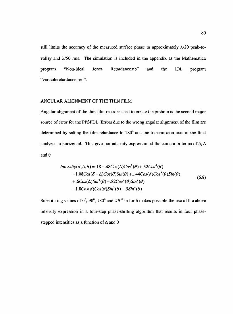
80
still limits the accuracy of the measured surface phase to approximately A./20 peak-to-
valley and A,/50 rms. The simulation is included in the appendix as the Mathematica
program "Non-Ideal Jones Retardance.nb" and the IDL program
"variableretardance.pro".
ANGULAR ALIGNMENT OF THE THIN FILM
Angular alignment of the thin-film retarder used to create the pinhole is the second major
source of error for the PPSPDI. Errors due to the wrong angular alignment of the film are
determined by setting the film retardance to 180° and the transmission axis of the final
analyzer to horizontal. This gives an intensity expression at the camera in terms of 5, A
and 0
Intensity{5, A, 0) =. 18 - .48Co5( A)Co5^ {6) + 32Cos'^ (0)
-1 .08Co5(^ + A)Cos(0)Sin(0) +1 A4Cos(S)Cos' (0)Sin(0)
+ .6Cos(A)Sm^ (6>) + .82Cos' (0)Sin' (0)
- L8Cos(^)Cos(0)Sm' (6)) + .SSin' (0)
Substituting values of 0°, 90°, 180° and 270° in for 6 makes possible the use of the above
intensity expression in a four-step phase-shifting algorithm that results in four phase-
stepped intensities as a function of A and 0

81
(6.9)
/, = .59 - .O9Cos(20) -. 18Cos(0)Sm(0) + .06Co5(A) (5=0°
- .54Cos(A)Cos(20) -1.08Cos(A)Cos(0)Sift(6))
+ .405Sm(46>)
= .59 + .06Co5(A) - .mCosiie) - .54CO5(A + 29) ^=90'
/j = .59 - .09Cos{2e) +. 1 %Cos{9)Sin{G) + .Q6Cos{A) S=l 80°
-.54Cos(A)Cos(20) +1 .OSCosiA)Cos(0)Sin(e)
-AO5Sin(40)
I, = .59 + .06Co5(A) - .O9CO5(20) - .54CO5(A - 29) 5=210°
Using these intensities in a four-step phase-shifting routine gives an equation for the
output phase at the camera as a fimction of the angle of the thin film, 0, and the surface
phase from the test optic, A
Output Phase = ArcTan MCosjA + 29) - MCosjA - 29)
{-.'i6Cos{9)Sin{G) - 2.\6Cos(,A)Cos{9)Sin{9)
+.8\Sin{49))
(6.10)
The difference between the input phase from the test optic, A, and the output phase at the
camera is a function of both the angular alignment of the film and the input phase. As in
the previous case, 0 is set to a value and A is varied from 0 to 2ti allowing for all possible
phases from the test optic to determine the phase error. Subtracting the input phase from
the output phase allows one to calculate the peak-to-valley and rms phase error for each
value of 0. Figure 6-3 gives the peak-to-valley and rms phase error for 0 ranging from -
37° to -47°.

82
Peak to Volley Phose Error yg, Retorder Angle 0.10
0,08
^ 0,06
0.02
0.00 -38 -36 -4S -46 -44
Ret a I -42 -40
Retorder Angle (In degrees)
RMS Phose Error vs. Retorder Angle 0.030
0.010
0.000 -36 -48 -46 -44 -42 -40
Retorder Angle (In degrees)
Fig 6-3: Peak-to-Valley and RMS Phase Error vs. Thin Film Alignment Angle
The minimum peak-to-valley and rms phase errors of 1.7x10"^ and 6.07x10'^ waves were
found at ^1.8° rotation of the thin film. With an ideal film retardance of 180°, the effect
of the diattenuation is corrected by rotating the thin film to -41.8° instead of -45°. The

83
simulation is included in the appendix as the Mathematica program "Non-Ideal Jones
Angle.nb" and the DDL program "thetaerrorl SO.pro".
ALIGNMENT OF THE ANALYZER
Angular alignment of the transmission axis of the final analyzer is the last major source
of error investigated. To determine the error due solely to the analyzer (j) is set to 180°
and aUgned at 0 = -45°. The only remaining source of error is the alignment of the
transmission axis of the analyzer. The result is an intensity expression at the camera in
terms of 6, A and vj/. The intensity expression is too long and complex to presented
directly in the text but is included in the appendix in the program "Non-Ideal Jones
Analyzer.nb".
Substituting values of 0°, 90°, 180° and 270° for 6 in the intensity expression permits
using the intensity in a four-step phase-shifting algorithm giving four phase-stepped
intensities as a function of A and v|/.

84
(6.11)
/, = 1.02 + .9Co5(A) -. 1 SCosiA - Ay/) - 3ACos{Aii/)
-. 1 5Co5(A + Ay/) - .6Sin(A - 2y/)
+ 2J2Cos{y/)Sin(y/) + .6Sin{A + 2y/)
=.635 + .33Co5(A) - .21Cos{A - Ay/) - .Q)A5Cos{Ay/)
- .51Sin{A - 2y/) +136Cos{}i/)Sin{}i/)
+ .035'M(A + 2y/)
I, = .25 - .2ACos{A) - .12Cos{A - Ay/) + .25Cos{Ay/)
- .\2Cos{A + Ay/)
I, = .635 + .33Co5(A) - .QA5Cos{Ay/) - .21Cos{A + Ay/)
- .03Sin(A - 2y/) +1.36Cos{y/)Sin{y/)
+ .57Sin{A + 2y/)
Using these intensities in a four-step phase-shifting routine gives an equation for the
output phase at the camera as a fiinction of the aUgnment angle of the analyzer and the
phase of the test optic
S=0°
5=90"
(5-180°
(5=270°
Output Phase = ArcTan (6.12)
.21Cos{A - Ay/) - .21Cos{A + Ay/)
+1.0%Cos{2y/)Sin{A)
.77 +1. 14Co5(A) - .03Co5(A - Ay/) -.59Cos{Ay/)
-.Q3Cos{A + Ay/) - .6Sin(A - 2y/) + .6Sin(A + 2y/)
+2.72Cos(y/)Sin{y/)
The difference between the input phase, A, and the calculated output phase at the camera
is a function of both the input phase and the angle of the transmission axis of the final
analyzer in the system. Like the other two cases, \\i is set to a value and A is varied from
0 to 2n to determine the error for all possible phases from the test optic for each value of
v|/. Subtracting the output phase from the input phase for all the A values allows

85
determination of the peak-to-valley and rms phase error for each value of vj/. Figure 6-4
gives the peak-to-valley and rms phase error for \\i ranging from 0° to -9.5°.
Peok io Volley Error vs. Analyzer Angle 0.40
S 0.30
0.20
0.10
0.00 - 1 0 -S - 6 -4 - 2 0 2
Anolyzer Angle
RMS Phase Error V 5 . Anolyzer Angle 0.025
0.020
g 0.015
0.010
0.005
0.000 - 1 0 - 8 - 6 -4 - 2 2 0
Anolyzer Angle
Fig 6-4: Peak-to-Valley and RMS Phase Error vs. Final Analyzer Angle

86
The minimum peak-to-valley and rms phase errors of .006 and .0003 waves are found at
^.4°. With a film retardance of 180°, rotating the transmission axis of the analyzer to -
4.4° from horizontal can significantly reduce the effect of the diattenuation. The
simulation is included in the appendix as the Mathematica program "Non-Ideal Jones
Analyzer.nb" and the IDL program "analyzererrorlSO.pro".
The simulations show two possible ways of correcting the phase error due to the
diattenuation in the films: rotate the film to ^1.8° instead of-45° from vertical or rotate
the transmission axis of the final analyzer to -4.4° from horizontal. While both methods
work well at correcting the phase error due to the diattenuation, rotating the retarder to -
41.8° provides the best result.
ACTUAL PPSPDI FILM WITH 160° RETARDANCE
The thin-film used in the PPSPDI was determined to have a retardance of 160° instead of
180° as desired for optimal system operation. To determine the error due only to this
incorrect retardance, 0 is set to -45° and the transmission axis of the final analyzer to
horizontal. The only source of error outside of the diattenuation in the film is the
incorrect retardance. Setting (j) to 160° gives an intensity expression at the camera in
terms of 5 and A
Intensity{d, A) = .59 + .09Cos{5) + .074CO5(A) + .525Cos{5 + A)
+. 131Sin{5) - .0825M(A) + m2Sin{d + A) ^

87
A value of (j) = 160° changes the heights of the four intensity values for 6 = 0°, 90°, 180°
and 270° and shifts the peaks relative to each other compared with the first simulation on
thin film retardance with (j) = 180°. This shift of the intensity peaks causes the 90° phase
steps to no longer shift the fi-ames by 90°. Figure 6-5 shows the four intensity values as a
function of A for 5 = 0°, 90°, 180° and 270° illustrating the intensity modulations between
frames and the incorrect phase shifts.
Intensity
0.8
180° 0.6
0.4 — — 270'
0.2
Surfece Phase A
Fig 6-5: Incorrect Phase Stepped Intensities As a Function of Surface Phase for ^ = 160°
For ([»= 160°, the four phase steps should be 0°, 107°, 198° and 271° for the four fi-ames to
all be 90° out of phase. Intelliwave, the software used to control the PPSPDI, can easily
accommodate the nonlinear phase steps. Intelliwave applies a voltage ramp to the
electrooptic modulator and watches the fnnges to determine 90° changes in phase at the
camera, regardless of the actual change in phase, 5, inside the modulator. At the same
time, Intelliwave is also able to overcome the intensity modulations between fi-ames by
contrast stretching the interferograms prior to calculating the phase. Figure 6-6 shows the

88
four phase-shifted intensities after the proper phase steps have been applied and the
intensities have been contrast stretched.
Intensity
Surface Phase A
Fig 6-6; Correctly Phase-Shifted Intensities with Contrast Stretching for (|) = 160°
After setting the correct phase steps and contrast stretching, the result is four 90° phase
stepped intensities that can be used in a four-step phase shifting routine.
I, = .5 + .5Co5(A)
107;r
d=0°
d=\QT
^=198°
(5=271°
(6.14)
= .5 + .0715Co5(A) + .246Cosi-^ + A) - .2645m(A)
/j = .5 - .234Co.s(A) - .266Cos(-^ + A) + .01185m(A)
O ^ 1 I, =.5 + .0837Cos(A) + .337Cosi-^ + A)
431;r - .270Co5(-^ + A) - .0922&«(A)
Using these four intensities in a phase shifting algorithm gives an equation for the output
phase at the camera as a function of the input phase of the test optic

89
Output Phase = ArcTan
.OUlCosiA) - .246Cos(^^ + A)
IIItt 431^ +.337Cos(^^ + A) - .270Co5(^^ + A) + .l72Sm(A)
180 180 179;r
.734Cos(A) + .266Cos(^^ + A) - .01185m(A) (6.15)
The difference between the input phase from the test optic and the calculated output
phase at the camera is a function of the input phase only. In this case, A is allowed to
vary between 0 and In to allow for all possible phases from the test optic. Subtracting
the output phase from the input phase allows the peak-to-valley and rms phase errors to
be calculated. Figure 6-7 gives the difference between the input phase and the calculated
output phase in waves for all input phase values between 0 and 271.
4.00*10 _ Difference Between Measured Phase ond Input Phose
3.95*10
3,90*10"'^
E 3.85*10
?? 3.80*10
3.75V10
3.70*10
Input Phose
Fig 6-7: Difference Between Input and Calculated Phase for (j) = 160° With Phase Step Correction and Contrast Stretching

90
This gives a peak-to-valley and rms phase error of 2.63x10"^ and 9.33x10'^ waves
respectively. Allowing hitelliwave to set the correct phase steps and stretch the contrast
of the four intensities gives almost ideal operation of the PPSPDI even with the incorrect
thin film retardance. The simulation is included in the appendix as the Mathematica
program "Non-Ideal Jones Retardance for 160.nb" and the BDL program
"errorfor 160plate.pro".
It must be remembered that the simulation above is an ideal case. The simulation looks
at only a single pixel with perfect phase steps and contrast stretching. The phase error
from the actual operation of the PPSPDI will not be this small. The instrument is not able
to phase shift as accurately nor contrast stretch as well as the simulation. With average
phase shifts of around 91° and rms phase shift errors of about 2° across all the pixels in all
frames, the PPSPDI operates with an rms phase error of .032 waves.

91
QUALITY OF THE REFERENCE WAVEFRONT
Just as any point-diffraction interferometer, the PPSPDI uses no reference optics; instead,
it relies on diffraction from a pinhole to create a spherical reference wavefr-ont.
Ultimately, the quality of this reference wavefront will limit the accuracy of the PDI
interferometer. Lawrence Livermore National Laboratory conducted research into the
quality of the PDFs reference wavefi"ont, but in each simulation the wavefr-ont incident
on the pinhole is assumed to be a uniformly illuminated plane wave (Goldberg 1996).
This is simply not a valid assumption since the amplitude and phase incident on the
pinhole are neither uniform nor planar and depend on the aberrations of the test optic.
This chapter focuses on the quality of the reference wavefront for a PDI as a function of
both incident aberrations from the test lens and pinhole size. Coma, spherical aberration
and astigmatism are investigated for pinhole sizes ranging from 50% to 150% of the
unaberrated Airy disk diameter of the test optic.
SIMULATION THEORY
This simulation begins in the same place as the scalar diffraction theory presented earlier,
i.e. the test lens. In this case, the test lens pupil fiinction is represented by a cylinder
function multiplied by an exponential phase term to include aberrations.
i2xw(xp,yp) (7.1)

92
where W(xp,yp) is the aberration function in units of waves with pupil coordinates Xp and
Yp ranging from 0 at the center to 1 at the edge of the cylinder
describing all first- and third-order aberrations with field dependence removed; thereby
allowing the simulation to accommodate all possible aberrations or combination of
aberrations. The optical field from the test lens is brought to focus at the PDI plate where
the focus spot formed is the Fourier transform of the lens pupil function. For this
simulation, the pinhole is assumed to have perfect transmission while the area outside the
pinhole has zero transmission. This allows investigation of the reference wavefront
independently of the test wavefront since the test wavefront is not transmitted by the area
around the pinhole. The field is multipUed by the pinhole, represented by a second
cylinder function with diameter di, that has the effect of spatial filtering the field prior to
the pinhole, removing the high frequencies and allowing transmission of only the lower
frequencies.
After the pinhole, the optical field propagates to the far field, mathematically represented
by a second Fourier transform of the field just after the pinhole. This is the same effect
as using a lens to image the field onto a camera just hke the actual operation of the
interferometer. Neglecting multiplicative constants, the optical field at the image plane is
W { x ^ , y ^ ) = + JV,,(x/ +y;) + + y/f
+ + y / ) y . + ^ 2 2 y / + + y / ) + K y , (7.2)
J2>iW(x2,y2)

U{x„y,) = d ,
93
(7.4)
where ** is a two-dimensional convolution across x and y. The propagation of the field
firom the test lens to the image plane is shown in Figure 7-1.
U(Xp,yp) U(x2.y2) UCxg.yg)
Test Lens PDI Plate Final Image Plane
Vf£_lZ£_^. jii'ifUp-yp) d ,
)n •e ^,(V5IZ)
Fig 7-1: Simulated Propagation of Reference Wavefiront
The simulation takes the optical field at the test lens including aberrations, Fourier
transforms it, multiplies it by the pinhole and inverse Fourier transforms. The amplitude
and phase of the optical field are recorded at each step.
There are two planes of interest in the simulation: the plane just prior to the pinhole and
the final image plane. Determining the amplitude and phase of the optical field prior to
the pinhole will verify under what conditions, if any, the current assumption of a uniform
plane wave striking the pinhole is valid. The variation in phase across the final image
plane gives the error in the reference wavefi-ont. The larger the variations in the phase,
the worse the quality of the reference wavefi"ont for the PPSPDI.

94
In the simulation, aberration values ranging from 0 to 6 waves of spherical aberration,
coma and astigmatism are applied to the test lens. In each case, the pinhole size is
allowed to vary from 50% to 150% of the Airy disk diameter. Each aberration can then
be analyzed separately as to its effect on the quality of the reference wavefront as a
function of aberration magnitude and pinhole size. The simulation is included in the
appendix in the IDL program "referencewavequality.pro".
SPHERICAL ABERRATION
Spherical aberration is the first aberration used in the simulation, and with spherical
aberration only, the lens pupil function becomes
where W40 is the number of waves of spherical aberration and the Fourier transform gives
the optical field just prior to the pinhole. Figure 7-2 shows the ampUtude and phase of
the field in front of the pinhole for 2 waves of spherical aberration where the effect of the
spherical aberration is radially symmetric so only the yp = 0 profile is shown.
(7.5)

95
X ProfM© of FFT ol the Pmhole 0.0006
0.0002 a
I
0.0000
0 50 100 150 200 X position (pixels)
X Profile Phose a1 ihe Pinhole 0.5
0.0
'ST
-0.5 u
I
-1.0
-1.5 0 100 50 150 200
X position (pivela)
Fig 7-2: Amplitude and Phase at the Pinhole For 2 Waves of Spherical Aberration
The red lines show the portions of the amplitude and phase incident on the pinhole with
diameter equal to 50% of the Airy disk diameter. With this diameter and amount of

96
spherical aberration, there is very little variation in amphtude and phase across the
pinhole so the assumption of an incident plane wave is valid. This assumption for the
50% pinhole does not hold true for all values of spherical aberration as the variations in
phase and amplitude change as the amount of spherical aberration is varied. Likewise, as
the pinhole size increases to 100% or 150% of the Airy disk diameter, shown by the blue
and green lines respectively, the variations in phase and amplitude increase and the
incident plane wave assumption is also no longer valid. While there are special cases
where the plane wave assumption is valid, in general when the test wavefront incident on
the pinhole contains even small amounts of spherical aberration the incident plane wave
assumption is invalid regardless of pinhole size.
After multiplication by the pinhole, the optical field is Fourier transformed to simulate
propagation to the final image plane. The peak-to-valley error of the phase of the optical
field across the final image plane is calculated and gives the maximum error in the
reference wavefront for the PPSPDI as a fiinction of pinhole diameter and amount of
spherical aberration. Figure 7-3 shows the reference wavefront error as a fiinction of the
amount of spherical aberration included in the simulation for pinhole diameters ranging
from 50% to 150% of the unaberrated Airy disk diameter of the test optic.

97
Wavefront Error vs. Spherical Aberration
(0 0 > 1
§ LU C p
I I
0.5
0.4
0.3
0.2
0.1
-0.1
-1
--T--T-r-r-i-T-^-r-i-p-r"r"r-r-y-T--T T-r- -T-T-r-T-
; ' /
: /• i ^ ' ' ' V /
i ''
i •; 1' ' : ?< ;
/ I ! / ; ' /
: /• i ^ ' ' ' V /
i ''
i •; 1' ' : ?< ;
/ I !
X \' 50% Airy disk
-Id— 75% Airy disk
'> 100% Airy disk
- -X -110% Airy disl< 125% Airy disk
150% Airy disk A
''
50% Airy disk
-Id— 75% Airy disk
'> 100% Airy disk
- -X -110% Airy disl< 125% Airy disk
150% Airy disk A
''
• ' ' ! ' 'i / '•
- ^ '
- .1
0'
t
'.
..
,
m
\
6 0 1 2 3 4 5
Spherical Aberration (waves)
Fig 7-3: Reference Wavefront Error vs. Spherical Aberration For Various Pinhole Sizes
While the wavefront error oscillates with increasing spherical aberration for all cases, the
average value and amplitude of the oscillation changes with pinhole size. For larger
pinholes, the wavefront error increases dramatically up to about 1 wave of added
spherical aberration, then levels off approaching .5 waves at 6 waves of added spherical.
There is a significant decrease in the amphtude of the oscillations with increasing
incident spherical aberration. For smaller pinholes, there is an initial peak in the
amplitude of the oscillation at .7 waves of added spherical aberration. Beyond this point,
there is a decrease in both the amplitude and average value of the oscillation with
increasing spherical aberration.

98
For a pinhole half the Airy disk diameter, the maximum wavefront error of .004 waves
occurs with .7 waves of spherical aberration added to the incident wavefront. This is the
point of maximum variation in the amplitude and phase incident on the pinhole shown by
the red lines in Figure 7-4. For pinhole diameters of 75% and 100% of the Airy disk,
given by the blue and green lines in Figure 7-4 respectively, the maximum wavefront
errors increase to .033 and .188 waves at .7 waves of added spherical aberration. This is
the point of maximum variation in amplitude and phase for these larger pinhole sizes as
well. It is apparent that for .7 waves of incident spherical aberration the amplitude and
phase across the pinhole for all diameters less than the Airy disk is neither uniform nor
planar and again invalidates the assumption of a uniformly illuminated plane wave
striking the pinhole.

99
X Proffle of FFT ol the Pfnhoie 0.0010
0.0005
OJ 3 Q.
J
0.0000
-0.0005 0 50 100
^ po?Uion (pivel«) 150 200
X Profile Phose oi Ihe Pinhole 0.5
0.0
-0.5
^ -1.0
-2.0
-2.5 0 50 100
X position (^y^s) 150 200
Fig 7-4: Amplitude and Phase at the Pinhole For .7 Waves of Spherical Aberration
Adding an equal but opposite amount of defocus to the spherical aberration to maximize
the Strehl ratio reduces the reference wavefront error for pinholes up to the size of the test

100
lens Airy disk diameter. The addition of the defocus has the effect of minimizing the rms
wavefront error at the pinhole. For a pinhole equal to the Airy disk diameter of the test
lens, the maximum reference wavefront error is .188 waves at .7 waves of incident
spherical aberration. By adding defocus, the maximum error in the reference wavefi-ont
is reduced to .046 waves at 2.5 waves of spherical aberration and -2.5 waves of defocus.
This is a factor of four decrease in the reference wavefront error. For pinholes larger than
the Airy disk diameter of the test lens, the effect of adding defocus to the incident
wavefront is negligible.
As shown above, the larger the variations in amplitude and phase across the pinhole, the
larger the error in the diffracted reference wavefront. While this is not an unexpected
result, it does give insight into why it is a common practice to create the PDI pinhole
where its diameter is no more than half the unaberrated Airy disk diameter of the test
optic. The smaller the pinhole diameter, the smaller the variations in amplitude and
phase across the pinhole are regardless of the incident aberrations. For a pinhole half the
Airy disk diameter of the test lens, the variations in amplitude and phase caused by
spherical aberration cause a maximum error in the reference wavefront of only .004
waves.
ASTIGMATISM
Astigmatism is the second aberration used in the simulation and looking only at
astigmatism the lens pupil function becomes

101
, y , ) = (7.6) d,
Where W22 is the number of waves of astigmatism added to the simulation. This function
is Fourier transformed to give the optical field just prior to the pinhole. Figure 7-5 shows
the amplitude and phase of the field in fi"ont of the pinhole for 2 waves of astigmatism.
Although astigmatism has its maximum effect along the y-axis, both Xp=0 and yp=0
profiles are shown as the effects on each axis is different.
X Profile of FFT ot the Pinhole Y Profile of FFT o1 1he Pinhole
0.0002
0.0000
•0.0002 0
aooio
0.0000
0
X Prollle Phose oi ihe Pinhole Y Profile Phase ol the Pinhole 2.0
0.0
1.6 0.2
» 1
1.0
•0-6
0.8
0.5
1.0
0.0 1,2 0 150 0
Fig 7-5: X and Y Profiles of Amplitude and Phase at the Pinhole for 2 Waves of Astigmatism

102
The red lines show the portions of the amplitude and phase incident on a pinhole with
diameter equal to 50% of the Airy disk diameter of the test optic. With this diameter and
amount of astigmatism, the amplitude is not uniform along either the x or y profiles and
only along the x profile is the phase approximated as planar. Once again, the immediate
conclusion is the incident plane wave assumption is invalid. As the pinhole diameter
increases to 100% or 150% of the Airy disk shown by the blue and green lines in Figure
7-5 respectively, even the possible assumption for the x profile phase is lost. In no way
can one make the assumption of a plane wave incident on the pinhole for 2 waves of
astigmatism regardless of the size of the pinhole. In fact, this holds true for all values of
astigmatism and pinhole size.
After multiplication by the pinhole, the optical field is Fourier transformed to simulate
propagation to the final image plane. The peak-to-valley error of the phase of the optical
field across the final image plane is calculated and gives the maximum error in the
reference wavefront for the PPSPDI as a function of pinhole diameter and amount of
astigmatism. Figure 7-6 shows the reference wavefront error as a fiinction of the amount
of astigmatism included in the simulation for pinhole diameters ranging from 50% to
150% of the unaberrated Airy disk diameter of the test optic.

103
Wavefront Error vs. Astigmatism . ' 1 ' M ' ' ' ' 1 ' ' ' ' p-T-r-Tn--
; : 7
; ; i A
- ^ \ X, X : ^ :
•• / ^
^ i - /•/-••I—
i - 50% Airy disk
"13-- 75% Airy disk
<> 85% Airy disk
- - X- -100% Airy disk 125% Airy disk 150% Airy disk - i' '' '<!•
'• k '
i - 50% Airy disk
"13-- 75% Airy disk
<> 85% Airy disk
- - X- -100% Airy disk 125% Airy disk 150% Airy disk - i' '' '<!•
'• k '
- 1 0 1 2 3 4 5 6 7
Astigmatism (waves)
Fig 7-6: Reference Wavefront Error vs. Astigmatism For Various Pinhole Sizes
hi this case, there appears to be two distinct functional forms for the wavefi-ont error for
pinholes less than the Airy disk diameter and pinholes equal to or greater than the Airy
disk diameter. While again the wavefi"ont error oscillates with increasing aberration for
all pinhole sizes, for pinholes equal to the Airy disk diameter and greater, the wavefi-ont
error increases sharply to about 1 wave of added astigmatism. Then the amplitude of the
oscillation decreases with the average value of the wavefi-ont error approaching .5 waves
at 6 waves of added astigmatism. For the smaller pinholes, the functional form is very
similar to the form found for spherical aberration with an initial peak around .7 waves of
added astigmatism and then a decrease in both the amplitude and average value of the
oscillation of the wavefront error with increasing astigmatism.

104
For a pinhole half the Airy disk diameter, the maximum reference wavefront error of .011
waves occurs with .7 waves of astigmatism added to the incident wavefront from the test
optic. Like the case for spherical aberration, this is the point of maximum variation in the
amplitude and phase incident on the pinhole shown by the red lines in Figure 7-7. For a
pinhole diameter 75% of the Airy disk given by the blue lines in Figure 7-7, the
maximum reference wavefront error increases to .09 waves for .7 waves of incident
astigmatism.
y Profile of f"FT ol the Pinhole Y Profile of FFT ol ihe Pinhole
0.0010
2 0.0005
a0000
0.0005 100
y povHion (piy«l«) 100
< peiil>on (pn«ls)
y Profile Phose oi Ihe Pinhole Y Profile Phoae ot the Pinhole
100 ( position (pveis)
Fig 7-7: X and Y Profiles of Amplitude and Phase at the Pinhole for .7 Waves of Astigmatism

105
With the sharp increase in error in the diffracted reference wavefront with increasing
pinhole diameter, the importance of constructing the PDI pinhole with diameter no larger
than half the Airy disk diameter of the test optic is apparent. While a maximum of .011
waves of error in the reference wavefront for the 50% Airy disk pinhole is not
spectactular, it is still significantly better than the .09 waves for the 75% pinhole and .5
waves for pinholes larger than the Airy disk diameter.
Coma is the last aberration used in the simulation. With coma only, the lens pupil
fiinction becomes
where W31 is the number of waves of coma added for the simulation. This function is
Fourier transformed to give the optical field just prior to the pinhole. Figure 7-8 shows
the amplitude and phase of the field in front of the pinhole for 2 waves of coma as an
example. The effect of the added coma is not symmetric so both the Xp=0 and yp=0
profiles are shown.
COMA
(7.7)

106
y Pfofite of TFT ol Ihe Pinhole Y Profile of Fn ai Ihe Pinhole
£ 0.0002
I
100 150 X position (piyffv)
100 150 Y posHiOn
X Profilf Phose ol the Pinhole
* posHloo {pl*el9)
Y Profile Phose ol the Pinhole
Y posHion (pixels)
Fig 7-8: X and Y Profiles of Amplitude and Phase at the Pinhole for 2 Waves of Coma
The red lines show the portions of the amplitude and phase incident on the pinhole with
diameter equal to 50% of the Airy disk diameter of the test optic. Even with two waves
of coma in the incident wavefront, the phase across the 50% pinhole is planar. The
variations in amplitude, especially across the y profile, keep the uniformly illuminated
plane wave approximation from being valid. As the pinhole size increases to 100% and
150% of the Airy disk diameter, shown by the blue and green lines respectively, the
variations in amplitude increase along both profiles. Under no circumstances of pinhole

107
size or incident amount of coma was the uniformly illuminated plane wave
approximation valid.
After multiplication by the pinhole, the optical field is Fourier transformed to simulate
propagation to the final image plane. The peak-to-valley error of the phase of the optical
field across the final image plane is calculated and gives the maximum error in the
diffracted reference wavefi-ont for the PPSPDI as a fiinction of pinhole diameter and
amount of coma added to the simulation. Figure 7-9 shows the reference wavefi-ont error
as a function of the amount of coma included in the simulation for pinhole diameters
ranging from 25% to 150% of the unaberrated Airy disk diameter of the test optic. The
pinhole diameter is reduced to 25% of the Airy disk diameter to successfully moderate
the errors induced by the added coma.

108
Wavefront Error vs. Coma
V>
1
LD
c 9
1 i
1.4
1.2
1
0.8
0.6
0.4
0.2
0
-0.2
,v\
1
i V r
" 1
i V r '•' 25% Airy Disk
- El -- 50% Airy Disk
<^' 75% Airy Disk
- - X - -100% Airy Disk 125% Airy Disk
A 150% Airy Disk
-
/
I: \ X ^X- N
'•' 25% Airy Disk - El -- 50% Airy Disk
<^' 75% Airy Disk
- - X - -100% Airy Disk 125% Airy Disk
A 150% Airy Disk
'•' 25% Airy Disk - El -- 50% Airy Disk
<^' 75% Airy Disk
- - X - -100% Airy Disk 125% Airy Disk
A 150% Airy Disk
/V-a /a - -^n-
-
0 1 2 3 4 5 6
Coma (waves)
Fig 7-9: Reference Wavefront Error vs. Coma For Various Pinhole Sizes
For coma there appears to be only a single functional form for all pinhole sizes. There is
an initial increase in the error to a peak occurring from .7 waves of coma for the 25%
pinhole to 1.2 waves for the 150% pinhole followed by the now expected oscillation of
the wavefront error with increasing aberration. The amplitude of the oscillation
decreases as the amount of added coma increases. Unlike the previous two cases, the
average value of the oscillations does not change with increasing aberration but remains
relatively constant. For a pinhole one quarter the Airy disk diameter, the maximum
wavefront error in the diffracted wave is .026 waves at .7 waves of incident coma. For a
pinhole half the Airy disk diameter, the maximum error increases to .14 waves at the
same .7 waves of incident coma, the point of maximum variation in amplitude and phase

109
at the pinhole for these pinhole sizes. This error is significantly larger than was found for
both spherical aberration and astigmatism for the same pinhole size.
From these results, the diffracted reference wavefront is much more susceptible to errors
due to coma in the incident beam than to either spherical aberration or astigmatism. For
both spherical aberration and astigmatism, the variations in amplitude and phase across
the pinhole are symmetric. This is not the case with coma, as the shift in the central peak
of the amplitude with increased aberration causes the amplitude variations across the
pinhole to be nonsymmetric. This difference could account for the increased sensitivity
of the reference wavefront to coma versus spherical aberration and astigmatism.

110
PPSPDIPPERFORMANCE, LIMITATIONS AND IMPROVEMENTS
This chapter finally gets to the point. How well does the PPSPDI actually work?
Performance is typically analyzed by examining both the accuracy and repeatability of
the instrument, and this will be no different. The accuracy will be determined by
comparing a measurement from the PPSPDI with a measurement from a commercial
fizeau interferometer. Comparing these measurements will verify the output of the
PPSPDI. By subtracting two measurements taken by the PPSPDI the repeatability of the
interferometer can be determined. Finally the limitations of the PPSPDI are discussed
with suggestions for possible improvements.
PPSPDI SETUP
Before the performance of the PPSPDI can be presented, the specifics of the actual
measurements must be discussed. The PPSPDI was set up as previously shown in Figure
4-1 with the spatial filter positioned at twice the focal distance in front of the test lens to
simulate a 4-f imaging system. The lens tested is a 42 mm diameter biconvex singlet
with 200 mm focal length giving an f-number of 4.75. In the 4-f configuration, the lens is
operating at an effective f-number of 9.5. Using a HeNe laser at .6328 |am, the
diffraction limited Airy disk formed at the rear focus of the lens has a diameter of 14.7
l^m. The pinhole used in the PPSPDI was etched into a silicon thin film retarder with a
retardance of 160° and 20% diattenuation. The pinhole diameter of 5 j4,m, 34% of the test
lens Airy disk diameter, was used to minimize errors in the reference wavefi-ont

I l l
improving the performance of the PPSPDI. Through its phase shift calibration routine,
Intelliwave was able to set the nonuniform phase shifts, discussed in the error analysis
chapter, required to shift the fi'ames by 90°. This is an automated process and the actual
shift in phase between fi'ames inside the electrooptic modulator is not known. The phase
measurement of the test lens is done using the 5B Schmidt/Creath algorithm, which uses
five frames to reduce errors due to incorrect phase shifts (Schmidt 1995). The five
interferograms are shown in Figure 8-1.

Interferogram #1 Interferogram #2
Interferogram #3 Interferogram #4
Interferogram #5
Fig 8-1: Five Interferograms For F/4.75 Biconvex Lens

113
Since there are intensity modulations between the frames, once hitelliwave acquires the
five frames, each firame is contrast stretched and normalized so that each fi-ame has the
same contrast before the phase information is calculated. The blue circles on the
interferograms show the area of the lens tested. Only about the center 70%, or 34 mm, of
the lens could be tested due to the combination of high fi-equency fnnges near the edges
of the interferograms and low contrast in interferogram #2. The combination of these
two factors made obtaining phase data outside the blue circles impossible even with the
software compensation for contrast.
MEASUREMENT ACCURACY
The accuracy of the PPSPDI is determined by comparing the results for the test lens
using the PPSPDI to the results of the same lens obtained using a commercial Wyko 6000
phase-shifting fizeau interferometer. Figure 8-2 shows the measurements of the lens
obtained by the two interferometers.

114
Measurement with the Wyko 6000 Phase- Measurement with the Polarization Phase-Shifting Fizeau Interferometer Shifting Point-Diffraction Interferometer
Fig 8-2: Comparison of Measurements of the Test Lens Using a Wyko 6000 Phase-Shifting Fizeau Interferometer and the PPSPDI
From the above pictures, the general shape of the test lens compares well. Table 8-1 lists
the seidel coefficients for spherical aberration, coma and astigmatism for the
measurements on both instruments and the difference.
Wyko 6000 PPSPDI Difference Spherical
Aberration (waves)
-5.182 -5.189 .007
Coma (waves) .363 .192 .171 Astigmatism
(waves) .329 .185 .144
Table 8-1: Comparison of Seidel Coefficients for Measurements on the Wyko 6000 Phase-Shifting Fizeau hiterferometer and the PPSPDI
The coefficients for spherical aberration compare favorably. While the coefficients for
coma and astigmatism do not compare as well, the differences can be attributed to
misalignment and tilt of the measured portion of the test lens from one instrument to the
other.

115
The difference in the astigmatism of .144 waves is caused by a difference in the tilt of the
test lens between the two measurements. Assuming there is no tilt on the test lens during
the PPSPDI measurement, the difference of .144 waves is due to a tilt in the test lens
when the measurement was made on the Wyko interferometer. Using Zemax, the test
lens was simulated in a 4-f imaging configuration and allowed to tilt. .144 waves of
astigmatism is induced at a tilt angle of .61".
Since the entire aperture of the lens was not tested, it is possible that the areas tested on
the two instruments are slightly shifted. This would account for the difference in the
coma values of .171 waves. The amount of misalignment necessary to induce this coma
is determined by taking the difference of two shifted spherical aberration terms and set it
equal to the coma difference.
W ^ { X p + y p f + + y p f = C o m a D i f f e r e n c e (8.1)
With Xp and yp equal to one, A is the percentage of the measurement area radius that one
of the measurements must be shifted to induce the coma. Substituting the values for W40
and the coma difference the equation becomes
-5.189-(l'+l')'-(-5.189)-((l + A)'+l)' =.171 (8.2)
This equation gives a solution of .0041 or .41%. With a measurement area radius of 17
mm, the shift in the two areas necessary to induce the .171 waves of coma is 70 |am.

116
INTERFEROMETER REPEATABILITY
The most important requirement when determining the performance of an interferometer
is the repeatabiUty of the instrument. The repeatability gives an indication as to whether
the interferometer results can be trusted from one measurement to the next. The
repeatability is determined by subtracting two consecutive measurements. Figure 8-3
shows the subtraction of the two measurements.
Fig 8-3: Subtraction of Two Consecutive Measurements
The resulting rms error is .032 waves. This gives a system repeatability of just under
A,/30. Careful inspection of the above plot shows that the peaks in the error occur in what
appear to be concentric rings occurring at roughly double the frequency of the fringes in
the original interferograms. The most obvious cause of this error in the repeatability is
phase shift errors in the two measurements. The average phase shift across all frames in
both measurements was found to be 90.85° with an rms error of 2.1°. A second possible
cause for the error in the repeatability is the contrast stretching done to the original

117
interferograms before the surface phase is calculated. While stretching the contrast of the
desired fringes, the contrast stretching also amplifies the noise in the interferograms.
Since each interferogram is stretched by a different amount, the noise in each will be
ampUfied by different amounts. Interferogram #2 is the most likely culprit for the
repeatability error since it required the most contrast stretching and therefore ended up
with the largest amplified noise.
LIMITATIONS AND IMPROVEMENTS
This final section will take a look at the limitations of the PPSPDI and suggest possible
improvements to the problems encountered in operating the interferometer. The two
biggest limitations in the operation of the PPSPDI are alignment error and the
birefiingent thin films used to create the pinhole filter.
Alignment error can be a big problem in operating the PPSPDI. Great care must be taken
when aligning the spatial filter, test lens and pinhole plate to ensure that all three are
aligned precisely along the optic axis of the interferometer. As was demonstrated in the
previous section on instrument accuracy, even a small tilt in the test lens or shift in the
measurement area produces significant artificial aberrations.
The most significant limitation in the PPSPDI is the birefiingent thin film used to create
the half-wave plate pinhole filter. The wrong retardance along with significant
diattenuation caused major problems in getting the PPSPDI to operate correctly. The

118
fluctuations in intensity and nonuniform phase steps caused by the incorrect retardance
and diattenuation taxed the abilities of both the operator and controlling software. The
films cannot presently be deposited accurately enough nor are they environmentally
stable enough for the PPSPDI to become a viable commercial instrument. Research must
be done into improving the accuracy of the deposition process and environmental
stability of the films. The only solution to reducing the diattenuation is to consider
different materials for the thin films. Other materials have lower diattenuation, but the
birefnngence will be lower as well. Manufacturing concems for etching deeper pinholes
will have to be considered when looking at the new materials.

119
SUMMARY
This dissertation describes the development of a new interferometer, the Polarization
Phase-Shifting Point-Diffraction Interferometer (PPSPDI). The PPSPDI uses a custom
pinhole plate made by etching a pinhole in a birefiingent thin film to separate the test and
reference beams based on their polarization states. Light from the test optic is brought to
focus on the pinhole in the film. The portion of light incident on the pinhole is diffracted
creating the reference wavefi^ont but retains its original polarization state. The remainder
of the light passes through the film, which is designed to be a half-wave plate, and its
polarization state is rotated by 90°. This allows the interferometer to interfere what were
originally orthogonal polarization components. An electrooptic modulator placed near
the laser source induces a variable phase shift between these orthogonal components
allowing for phase shifting.
The pinhole plate was manufactured by etching a pinhole into a bidirectionally deposited
thin film. Ideally these films can be deposited to provide retarders of any specific
retardance. For the PPSPDI the films were designed to be half-wave plates. Several
methods were used to attempt to etch the pinhole including argon ion milling, reactive
ion beam etching and focused ion beam etching. The focused ion beam etching
technique proved the most successful giving an etch resolution of 12 nm and feature
profiles vertical to 3°. Unfortunately, not only were the films not half-wave plates but

120
included diattenuation as well. The best of the supplied films was used having a
retardance of 160° and 20% diattenuation.
The incorrect retardance and diattenuation in the film caused significantly more problems
than expected. A phase shift in the electrooptic modulator of 90° no longer guaranteed a
phase shift of 90° in the interferogram. The nonuniform phase shifts in the modulator
required to shift the frames correctly caused problems in calibrating the instrument,
hitensity modulations across the five fi-ames, again due to the films, limited what could
be tested.
Considering the problems with the thin films, the PPSPDI's performance exceeded
expectations. The measurement of the test lens on the PPSPDI compared favorably with
the result for the same lens on the commercial interferometer. Subtracting two
consecutive measurements demonstrated a measurement repeatability of better than X/30.
Correcting the problems with the thin films would significantly improve the performance
of the PPSPDI.

121
APPENDIX A
Non-Ideal Jones Matrix.nb
Non-Ideal Jones Matrix.nb
Wntten by Mark Neal
26 March 03
This progan performs the Jones matrix propa^ion to obtain a general form for the intensity at the camera
for the PPSPDI. This program does not give values to any of the variables except for the beam balance fector
A which is given a value of .6. This progam gpes with the section "Nonideal Jones Matrix Propa^ion" in
the diaptff on error analysis.
The first few oonmands ensure that all the variables are real.
Conjugate [0]
Ccnjugat»[e] "=61
Oanjugat»[S] ''s 61
Oonji]gat»[A] ^=a;
acnjugat:e[(/r] *= t(r;
OGnjugate[A] A;
A= .6;
The next expression is the Jones matrix propa^ion for the test beam of the PPSPDI as given in the emor
analysis chapter for the nonideal propa^ion.
TestBeams
Sinclifvl—.( C303[«*Sln[((r] ^ , Cos[-e] Slii[-e]» / .8e^» 0\ I aoaie] Sln[e]v
^ ^ ^ ^ 2 l a o s [ « * s i i i [ i / r ] r \ - s i i i [ - e ] c o s [ - e ] / - l 0 i j ' U s i i i [ e ] a o s [ e ] / '
Co' ;.)•(;
' ei'^Cbe[ifl (sin[s] (o.Sei a»|e-«+Sinie-i('l)+a)e[ei (o.8ei*a>s(e-«-ei'5sin[e-«)
V 2 (sliiiei (o.8e^ oo6ie-»iH-siii[e-»i)->ca6[ei (o.8e''<'036[e-»i-e''^ain[e-iA])) sini»i
V 2
This expression is the reference beam for the PPSPDI
RefereaceBeam=»atrixJV>m[-i_J Gos[W *Sln[« Wl 0 | ^ ^ 2 \ O o a [ m * S i n [ i l f ] S i n l i l / r I \ 0 \ A / J
0.6Cb6[i/r]2+0.6e^'^0:)S[i^] SiJi[{/f]
0.6006tiA} Sin[(/f] +0.6e^'^ Sin[</f]^
V2

122
The total anplitude at the canm is just the addition of all four conponents of the test and reference beams (an x and y conponent for each beam).
TotalAnplltuds::TestSeam[[l, 1]] -fTestBeamtCl, 2]] -f Re£erenceBeam[[l, 1]] -f Rs£erenceBeam[[X, 2]]
, e''^Cos[i/'l (sin[el (0.8e'Cos[e - i/;] + Sin[e - i/-]) + Cios[e] (0.8 e'^Cos[e - i/f] -Sin[e - i/r]))
1 vi
(Sin[e] COBie- III] +Sin[e-)A]) +Cos[e] (0.8 e^*Cos[e - lA] -e*''Sin[e - i/r])) Sin[i//1 _ ,
0.6C!os[i/r]2+0.6c'''cos[i/(] Sin[i/(] 0.6CO3[iA] Sin[iAl <- 0.6 Sin[i/f] ^
V"2 /2 ^
The total intensity at the camera is the total anplitude nultipliedl^ its conplexconjugite.
]htenslt:y= Slnpllfy[B)ipand[TotaUiii>litude* Conjugate [TotedAnplltude] ] ]
{C!OS[e]^ (Cos[e-if]^ ((0.32+ O. i) + (0. + 0. i) Cos[2i/f] + (0.64+ 0. i) Cos[i(f] Sin[iA]) +
^-i(5+<.) cos[e-</*] Sin[e-iA] (-0.4Ctos[i/f]^-0.8Cos[<A] Sin[i/(1 - 0.4 Sin[(/(]^) +
Sin[e-</(]^ (0.5C3os[</(]^+ 1. Ctos[i/(] Sin[(/(] + 0.5 Sin[(/f]^)) +
Q^gjgj (0.32e'"'"^l (l+e^'"^) CDS[e-i/<]^Sin[e] (1. a5S[i/r]^+2. Cos[iA] Sin[i/(1 + 1. Sin[i;']^) +
Ctos[e-<A] (0.24 (1+ Cost</']^+ (0.48 + 0.24 + 0.24 + 0.48 e') Cos(iAl^Sin[</(] +
(0.24e"+ 0.48e^'''+ 0.486^'"^"^' + 0.24 c*) C!os[i/f] Sin[(A]^ + 0.24 Sin[i/i]^) -
0.3e''''Sin[e- If] (l. (1+ Cos[<«^ + 2. (l. + 0.5 + 1. + 0.5c') Cos[)/rl^ Sin(</(] +
1. e''^ (1 + Sin[i/r]^ +
03S[|A] SinliA] (3.33333 (1 + Sin[0] Sin[e- i/r] +1. (l. + 2. + 1. '''*'^' + 2. ) Sin(<;f]))) +
^-i(5+A+0) (o.iSe"''*''**' Cos[iJ']''+Cos[iA]^ (0.24 C3os(e-iAl Sin[e] +
0.18 e'* (1.66667 (l+ Sin[e] Sin[e - ij/] + 1. (l. + e''^) (l. + e*^) Sin[iji])) +
Oosli//] sinlil/] (0.64e'''^'^**'Cosie-i;/]^Sin[el^ + Cos[e-i;fl Sinie] (0.8 (l + ) Sinie) Sin[e-i(il +
0.24 (1. + 2. e*''+ 1. +2. gi <'5»2 (&•<•) I j sin(i/r]) + 0.3e^* (3.33333 e'Sin[ej Sin[e - </*) ^ +
(1. c"+ 2. e^^'^+ 2. e^*''+ 1. Sin[e) Sin[e - lA] Sin[iA] + 0.6 (l. + 2. + 1. Sin(iA]^)) +
Sin[iJ']^ (0.32 6^"'*'^*''" Ctis [e-iir)^ Sinie] +Cos [e-i/(] Sin(e] (0.4c''' (l + ) Sin[e] Sin[e - i*'] +
0.24 e" (l + e^'Sin[i;(]) + 0.3e'''' (1.66667e'Sin(e)^Sin[e - <A]^ + 1.
Sin[ei Sin[e-i/f] Sin[)/(] - 0.833333e'''(l. (l + e^'"®) Sin[2e] Sin(e - lA] ^ - 0.72 e" Sin[i<'l ^))) +
a3S[i/*]^ (0.32e^''^*^*'^' Cos(e- )/t]^Sin[ei^ + Oos[e-)A] Sin[e] (0.4 e''* (1 + Sin(el Sin[e- i//] +
0.48 (1. + 0.5e''^+ 1. e^'+0.5 6*"'^^"^*'''" ) Sin[i/(]) +
0.6c'''' (0.833333 Sin[e] Sin[e - lA] ^ + (l. e''^+ 0.5e^''^+ 0.5c^'''+ 1. ) Sin[ei
Sin[0-<//] Sin[iA] - 0.416667 c*'^ (l. (l + c^'"') Sin[2e] Sin[e - iM ^ - 1.44 (l+ c'''+ c^") Sin[i/f]^))))}

123
Non-Ideal Jones Retardance.nb
Non-Ideal Jones Retardance.nb
Wntten MarkNeal
26 Mar 03
This progmi performs the Jones matrix prop^ion to obtain the form of the intensity at the camera and the output phase
of the interferometer as a function of the retardance of the thin film This progwn gives the ideal values to the alignment
angles of the thin film and final analyzer. This prog^ gpes with the section "Retardance of the Thin Film" in the error analysis diapter.
The first few contnands ensure that the variables are all real
« Gcc^dilcs'liegend''
Oonjugate[0] <t>;
Oanjv]gate[e] *= 0;
Q»jugata[5] *= 5;
Catijugate[A] ^=a ;
Ocxijugat;e[i/r] '"s i/r;
Conjugate [A] ^=A;
The next eqjression is the Jones matrix representation for the test beam of the PPa'DI given in the enx)r analysis diapter.
TestBeam =
>&itxlxFom[
Slnolifyf — . ( Ctos [((r] • Sin[./f] ^ / Cos [ -e] Sin[-ei laos[iA] *Slii[|^3 sia[ilr]^ j' \-Sin[-e] a3S[-e] (•r ;)•(-aos[e] sin [6]
Sin [6] Cbs[e]
:mi Mi (sin|91 (o.8e'Cbeie-i»l*Sin[9-»l)-tQ)B[91 (o.8e''<'CbB|e-i»l-e''^Sln[e-i»l))
Va
(SiJi[e] (o.8e^ Oj6[e-i^i+Sin[e-iAl)-fClo6[0] (o.8e^^C336[e-iif)-e^'^Sin[0-t;f])) Sin[i^l
•si 2
This expression is the reference beam for the PPSPDI
Referenc^=»^txl^[^.( OosW *Sin[,^] | (1 0 | *•^2 VCos[i^] *Sln[t/r] Sln[|^]' J VO VA/J
AOs6[i/')2+Ae*'^C06(t/f] Sin[iAl
V2 AQ:e[i^l Sinfi^l+Ae''^ Sinti/'l2
V 2

124
The total amplitude is just the addition of all four components of the test and reference beams (an x and y
component for eadi beam)
TbtalAnplltude= TestBeain[[l, 1]] +TestBeam[[1, 2]] + Re£erenc^Beam[[l, 1]] -i-KeferenceBeani[[l, 2]]
{ e''^Oos[i/f] (Sin[ei ( 0 . 8 e ' O o s [ e - i / ^ ] + S i n [ e - i / ^ ] ) + O o s [ e ] ( 0 . 8 e ' ' ^ a ) s [ e - - e * ' ' S i n [ e - i / * ] ) )
VI
(Sin[e] (O.Be* Cos[s-(/f] +Sin[e-(//]) +Cos[e) (0.8 e*'''Cos[e - Vl S±n[e - i t ] ) ) Sin[(//] +
A (JO S [I/(]^ + A e^'Oosli/'] Sin[(/*] ACjOS[I/F] Sinl i l t ] + Ae^'^ Sinli/F]^ + }
4^
The total intensity at the camera is the total amplitude multiplied ty its cwnplex conjure This is where the ideal values
for the thin film and analyzer angles are set. The thin film angle is set to -45 deg«s and the analyzer is set to 0 degrees.
The beam balance f^or is set to .6.
Setardanceliitensity[£_, A_, 0_] =
C3icp[E]qpTtfr]:ig[E]3)and[TotalAnplltude*CcnjugatB[Tot:alftnplltiide]]]] / . A-> .6/. S-> — / . i/r-> 0 4
{0.59+ 0.09aos [ a ] + 0 . 3 C o s ( A ] + 0 . 3 C o s [ 5 + A ] + 0.2 Cos [ 5- 0 ] - 0.2 Cos [ < 5 + 0 ) + 0.24Co s ( a + 4>] - 0.24 Cos [ < 5 + A + 0 ] )
The four phase stepped intensities are found by inserting the proper values of0,90,180 and 270 d^^ in for the phase
step variable.
Ketasdancel-aiC{)[Siirpllfy[RetardanceInt:eiisit:y[0, A, 0]]]
{0.68+ 0.6COS [ A ] }
Retardeu:ice2 ^ CtK{>[Siiipllf/[KetardanceInteinslt:y[y, ^' ^] ]]
(0.59+ 0.3 Cos [ A ] + 0.24Cos [ A + ( < i ] - 0.3 Sin [ A ] + 0 . 4 S i n [ < < ) ] + 0 . 2 4 S i n [ A + < J ] )
Ketan3aiice3 = CtK{>[Sliipll£y'[Setardaz]cemtenslty[7r, A, 0] ] ]
{0.5+0.48 CO8 [ A + 0 ) )
Bet:azdance4 = Cb3p[Sli[pllfy'[lietardaiiceIntenslt7[-^, A, 0] ] ]
{0.59+0.3 Cos [ A ] +0.24 Cos [ A + 0 ] + 0 . 3 S i n [ A ] - 0.4 Sin[01 - 0.24 Sin [ A + i< i ] }
The four intensities are then put into a 4 step phase shifting routine to calculate the output phase fixm the interferotneter
as a function of the retardance of the film and input phase fhim the test optic. This is the equation used in the IDL program
to find the enw in the output of the interferometer.
Bet:azdancePhase = Siiipllfy[ArCTan[ Cbc|)[Ketardance4 - Ket;ardaiice2] Chop[Ret:arclancel - Retaxdance3]
0.6Sin [ A ] -0.8Sin[<<)] - 0.48 Sin [ A + 0 ]

125
$DefaultPoiit = {"Arial", 17}
{Arial, 17)
This plots the four intensities as a fimction of iqjut phase ikan the test optic for the perfect case of a half-wave plate
{ A , 0, 2 t t} , AxesStyle -> lhickness[ .004],
FlotStiyle-* {(AbsoluteEaildaiess[2], KGSOolar[l, 0, 0]},
{Absolut:eaMc]aiess[2], Dasliijig[{.015, .015}], R3Baolor[0, .5, 0]},
(Absolute(Iliic]aiess[2], Dashing[{.025, .025}], RGBColor[0, 0, 1]},
{Absolutenblc]a]ess[2], DaB>iing[{.05, .05}], KGB0olor[.5, .5, .5]}},
AxesLsdsel^ {"Surface Sbase A", latensity}, Plotiegend-» {"Ii", "I2", "I3", "I4"},
IiegendPosltlcxi-* {.65, -.3}, IiegendSlze-> {.6, .6}, Lec|ecidSbadc«r-» Nboe]
Intensity
1.2 1
0.8 0.6 0.4 0.2
Il
I2
I3
- - I 4 Surface Phase A
1 2 3 4 5 6

V ariableretardaiice.pro
pro variableretardance
;Written by Mark Neal on 26 Mar 03
;This program calculates the error due to the PDI plate being the wrong retardance ;and includes diattenuation. It is assumed that the retarder is at 45 degrees and ;the analyzer is horizontal. The analytic solution was obtained using a ;Mathematica program with the filename "Non-Ideal Jones Retardance.nb"
;Define the arrays used device, decompose=0 k=100 stepl=fltarr(k) step2=fltarr(k) step3=fltarr(k) step4=fltarr(k) phase=fltarr(k) difFerence=fltarr(k) Ideal=fltarr(k) delta=fltarr(k) i=con:q)lex(0,l) sxu:f=fltarr(k) phi=fltarr(k) niaxx=fltarr(k) minn=fltarr(k) error=fltarr(k) stddeviat=fltarr(k)
;Loop through retardance values for m=0,k-l do begin phi(m)=double( 160+(.4*m))*(!pi/180.0)
;Loop through input siurface phase from 0 to 2pi. If perfect then the output of the program will ;be exactly this value for n=0,k-l do begin surf(n)=double((2.0*!pi*(n))/k)
;This is the analytic solution from Mathematic for (I4-I2)/(I1-I3). So, the output phase is the ;Arctangent of this value. phase(n)=Atan((.6*Sin(surf(n))-.8*Sin(phi(m))-.48*Sin(surf(n)+phi(m)))/(.18+.6'''cos(surf(n))$ -.48*cos(surf(n)+phi(m))))
endfor
;Plot the unwrapped output phase and wrapped input phase in radians. window,! plot,surf,phase, Background=255,color=0,title='Measured Phase vs. Input Phase',$ xtitle-Input Phase',ytitle-Measured Phase' oplot,surf,Atan(T an(surf)),color=0

127
;Unwrap the output phase to remove phase ambiguities. for n=0,98 do begin if (phase(n) gt 0.0) and (phase(n+l) gt 0.0) and (phase(n+l) gt phase(n))$ and (abs(abs(phase(n+l))-abs(phase(n))) gt .8) then phase(n+l:*)=phase(n+l:*)-!pi if (phase(n) gt 0.0) and (phase(n+l) gt 0.0) and (phase(n+l) le phase(n))$ and (abs(abs(phase(n+l))-abs(phase(n))) gt .8) then phase(n+l:*)=phase(n+l:*)+!pi if (phase(n) gt 0.0) and (phase(n+l) le 0.0) and (abs(abs(phase(n+l))+phase(n)) gt .8)$ then phase(n+l :*)=phase(n+l :*)+!pi if (phase(n) le 0.0) and (phase(n+l) gt 0.0) and (abs(phase(n+l)+abs(phase(n))) gt .8)$ then phase(n+l :*)=phase(n+l :''')-!pi if (phase(n) le 0.0) and (phase(n+l) le 0.0) and (phase(n+l) gt phase(n))$ and (abs(abs(phase(n+l))-abs(phase(n))) gt .8) thenphase(n+l:''')=phase(n+l:*)-!pi if (phase(n) le 0.0) and (phase(n+l) le 0.0) and (phase(n+l) le phase(n))$ and (abs(abs(phase(n+l))-abs(phase(n))) gt .8) then phase(n+l:*)=phase(n+l:*)+!pi endfor
;Plot the output phase in radians. window,2 plot,surf,phase,Background=255,color=0,title-Measured Phase vs. Input Phase',$ xtitle-input phase',ytitle='Measured Phase' oplot,surf,surf,color=0
;Plot the difference between the output phase and the input phase in radians from the surface. difiFerence=phase-surf window,4 plot,sxuf,difference,Background=255,color=0,$ title-Difference Between Input Phase and Measured Phase',xtitle-Input Phase',ytitle-Difference'
;Find the maximiun, minimimi, max-min and standard deviation for the difference of the input and output phase. maxx(m)=max(difference) minn(m)=min(difference) error(m)=maxx(m)-minn(m) stddeviat(m)=stddev(difference,/double,/nan) ;Print the peak to valley and rms error in waves for each value of retardance. print,(180/!pi)'''phi(m),' peak to valley error in waves ',(l/(2*!pi))'''error(m) print,(180/!pi)'''phi(m),' rms error in waves ',(l/(2'''!pi))*stddeviat(m) endfor
;Plot the peak to valley and rms error in waves vs. retardance window,5 plot,(180/!pi)'''phi,(l/(2'''!pi))'''abs(error),Background=255,color=0,title-Peak to Valley Phase Error vs.$ Retarder TTiiclmess'.xtitle-Retarder Thickness (in degrees)',ytitle-Peak to Valley Error (in waves)' window,6 plot,(180/!pi)'''phi,(l/(2*!pi))'''abs(stddeviat),background=255,color=0,title-RMS Phase Error vs.$ Retarder Thickness',xtitle='Retarder Thickness (in degrees)',ytitle='RMS Error (in waves)'
end

128
Non-Ideal Jones Angle.nb
Non-Ideal Jones An^e.nb
WWtten by MarkNeal
26 Mar 03
This progFam performs the Jones matrix propagation to obtain the form of the intensity at the camera and the output
phase of the interferometer as a fimctionof the an^e of the thin film retarder used in the PPSPDI. This progan uses
the ideal values for the film retardanoe and the an^ of the final analyzer. This progam also gives the four phase-stepped
intensities and the output phase of the interferometer as a function of the an^e of the film This progan gpes with the
section "Angilar Aligiment of the Thin Film" in the error analysis ch^ter.
The first few corrmands ensure that the variables are all real.
Ocajugat:e[0] tt>i
aonjugate[e] '^= 6;
Conjugate [d] 6}
Ccnjugate[A] A;
Clanjugate[t^] *= ilii
Ocajugate[A] '^=A;
This expression is the Jones matrix rqjresentation for the test beam of the PPSPDI from the error analysis dieter.
TtotBeems
HatxlxFann[
sWifvf— ( Oos[Kr]*Sln[((r] ^ , aos[-e] Siji[-eiv f . ee^* 0 ) / CO3[0] Sin[e]\ Bjupj-iiyi laos[^].sin[M Siii[^]2 rUsin[-e] aoshe])-^ 0 ij'Usin[ei C3os[e]r
(stoiei (o.8e» 036te-i»itSuiie-»l)«Cbs[9i (o.8e''<'Ct»[e-»i-e''^Sln[9-»|))
e'^(sin[ei (0.6e'006[6-»l-i-Sln[9-»l)-tO0B|ei (o.8e''*'COs[e-»l-ei'^Sln[9-»l)) sln[i»l
y/ 2
This expression is the reference beam for the PPSPDI.
1 ^ f Coa[ilr]^ Oos[ilr]*3i
.^2 * VOos[« *Sin[i/r]
Oos[<A] *Sin[i/r] )•(; AOoeiij/j^+Ae^^CceiiJr] Sin[tA]
V 2 AO06[i^l Sin[{A]+Ae^'^ Sin[i/f)2
V 2
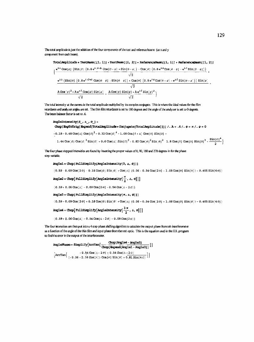
129
The total anplitude is just the addition of the four components of the test and reference beams (an x and y
oonponent fixmeadi beam).
IbtalAnplltnides TestBeam[ [1, 1] ] +TestBeam[ [1, 2] ] + Re£erenceBeam[ [1, 1] ] + KeferenceBeam[ [1, 2] ]
, e*'^Cos[i//] (Sin[e] (0.8e* Cos[e-)//]+Sin[e - i/^])+Cos[8] (0.8e»^Cos[e - <A] - S i n [e- ( / / ] ) )
I vi (Sin[e] (0.8e*<'5"^' Cos[e-i/*] +Sin[e-i//]) +Cos[e] ( 0 . 8 e ' ^ C o s i e - i/f] - e" Sin[e - lA])) Sin[i/-]
The total intensity at the camera is the total amplitude multiplied by its complex conjure. Thisis where the ideal values for the film
retardance and analyzer an^es are set. The thin film retardance is set to 180 degties and the an^e of the analyzer is set to 0 degrees.
The beam balance factor is set to .6.
Anglelnt:enslty[£_, A_, e_] =
a]cp[E]^itroTrig[Ea^>and[Tot:alhipllt:ude*acnjugate[Totalftiiplit:ude]]]] /. .6/. 0-> tt/. 0
jo.is- 0.48 Cos [A] Cos[el^+ 0.32Cos(e]^ - 1.08Cos[C5 + A] Cos[e] Sin[ei +
1.44Cos[6] Cos[e]^Sin[e] + 0.6COS[A] sin[e]^ + 0.82 Cos[ei^Sin[e]^ - 1.8 COS[<5] Cos[e] Sin[e)^ + ] 2 >
The four phase stepped intensities are found by inserting the proper values of0,90,180 and 270 d^iees in for the phase
stq> variable.
Anglels C3Kp[FallSliipll£y[Anglelnt;enslty[0, a, d}]]
{0.59- 0.09Cos[2 0] - 0.18 COS[0] Sin[0] +Cos[A] (0.06 - 0.54 Cos[2 S] - 1.08 Cos[0] Sin[0]) + 0.405 Sin[4 0]}
Angle2 = (3x:p[ E\illSiiipllfy[AngleIiitensity[ 3] ] ]
( 0 . 5 9 + 0 . 0 6 C o s [A] - 0.09 Cos [2 0] - 0.54 Cos[A + 2 0] }
Angles = Chop[FullSiiipllfy[AngleInt:enslty[7r, a , e] ] ]
{0.59- 0.09 Cos[2 0] t 0.18 Cos[0] Sin[0] +Cos[A] (0.06 - 0.54 CDs[2 0] + 1.08 Cos[0] Sin[0]) - 0.405 Sin[4 0]}
Angle4 = (3x:p[FVillSini>llfy[AngleIntenslty[^^, s] ] ]
{ 0 . 5 9 + 0 . 0 6 O o s [ A ] - 0 . 5 4 C o s [ A - 2 6 ] - 0 . 0 9 C o s [ 2 0 ] ]
The four intensities are then put into a 4 step phase shiflingalgarithm to calculate the output phase from tdi interferometer
as a fimction of the an^e of the thin film and input phase fiwri the test optic. This is the equation used in the IDL progam
to fmd the error in the output of the interferometer.
+
V2
ACos[iA]^ + Ae^''Cos[i<f] Sin[)A] ACos[i//] Sin[iA] + Ae*'^ Sin[i/f]^
J^iei%aae = Siiipllfy[AixTan[ Q)cp[Angle4 - Angle2]
-0.54 Cos [A - 2 0] + 0 . 5 4 C o s [A + 2 0] (-0.36-2.16Cos[A]) Cos[e] Sin[e] +O.81Sin[40]

130
This plots the four intensities as a fimction of input phase fiiom the test optic for the ideal aligiment of the retarder
at-45d^iees.
Flotf (Anglel / . e - > —, Aiigle2 /. e -> — , Angle3 / . e - > — , Angle4 /. 6 -> — }, {A, 0, 2 tt} , 11 4 4 4 4 J
PlotStyle^ {{RGBaolor[l, 0, 0]), {RGBOolorLO, .5, 0]), {RGBaolar[0, 0, 1]), {RffiCtolorC.5, .5, .5]}},
Axesliidbel-> {SurfaceBhaseA, Intensity}]
Intensity
1.2
0.8
0.6
0.4 •-/' 0.2
E^iase Surface A

131
thetaerrorl SO.pro
pro thetaerrorl 80
;Written by Mark Neal on 26 Mar 03
;This program calculates the error due to the PDI plate being at the wrong angle ;and includes diattenuation. It is assumed that the film has a retardance of 180 degrees and ;the analyzer is horizontal. The analytic solution was obtained using a ;Mathematica program with the filename "Non-Ideal Jones Angle.nb"
;Define the arrays used device, decompose=0 k=100 num=fltarr(k) denom=fltarr(k) step3=fltarr(k) step4=fltarr(k) phase=fltarr(k) di£ference=fltarr(k) Ideal=fltarr(k) delta=fltarr(k) i=complex(0,l) surf=fltarr(k) theta=fltarr(k) maxx=fltarr(k) minn=fltarr(k) error=fltarr(k) stddeviat=fltarr(k)
;Loop through the angle of the retarder for m=0,k-l do begin theta(m)=double(-46.7+(. 1 *m))*(!pi/l 80.0)
;Loop through surface phase from 0 to 2pi. If perfect then the output of the program will ;be exactly this value. for n=0,k-l do begin surf(n)=double((2.0* !pi*(n))/k)
;This is the analytic solution from Mathematica for 14-12. num(n)=-.54*Cos(surf(n)-2*theta(m))+.54*Cos(surf(n)+2*theta(m)) ;This is the analytic solution from Mathematica for 11-13. denom(n)=(-.36-2.16*Cos(surf(n)))*Cos(theta(m))*Sin(theta(m))+.81 *Sin(4*theta(m))
;The output phase is the Arctangent of (I4-I2)/(I1-I3). phase(n)=Atan(num(n)/denom(n))
endfor
;Plot the wrapped output phase and wrapped input phase. window,! plot,surf,phase,Backgroimd=255,color=0,title='Measured Phase vs. Input Phase',$
132
xtitle-Input Phase',ytitle='Measured Phase' oplot,surf,atan(tan(surf)),color=0
;Unwrap the output phase to remove the phase ambiguities. for n=0,98 do begin if (phase(n) gt 0.0) and (phase(n+l) gt 0.0) and (phase(n+l) gt phase(n))$ and (abs(abs(phase(n+l))-abs(phase(n))) gt .8) then phase(n+l:*)=phase(n+l:*)-!pi if (phase(n) gt 0.0) and (phase(n+l) gt 0.0) and (phase(n+l) le phase(n))$ and (abs(abs(phase(n+l))-abs(phase(n))) gt .8) then phase(n+l:*)=phase(n+l:*)+!pi if (phase(n) gt 0.0) and (phase(n+l) le 0.0) and (abs(abs(phase(n+l))+phase(n)) gt .8)$ then phase(n+l :*)=phase(n+l :*)+!pi if (phase(n) le 0.0) and (phase(n+l) gt 0.0) and (abs(phase(n+l)+abs(phase(n))) gt .8)$ then phase(n+1: *)=phase(n+1: *)- !pi if (phase(n) le 0.0) and (phase(n+l) le 0.0) and (phase(n+l) gt phase(n))$ and (abs(abs(phase(n+l))-abs(phase(n))) gt .8) thenphase(n+l:*)=phase(n+l:*)-!pi if (phase(n) le 0.0) and (phase(n+l) le 0.0) and (phase(n+l) le phase(n))$ and (abs(abs(phase(n+l))-abs(phase(n))) gt .8) thenphase(n+l:*)=phase(n+l:*)+!pi endfor
;Plot the unwrapped output phase and incident phase. window,2 plot,surf,phase,Background=255,color=0,title-Measured Phase vs. Input Phase',$ xtitle-input phase',ytitle-Measured Phase' oplot,surf,surf,color=0
;Plot the difference between the output phase and the input phase from the surface. difference=phase-surf window,4 plot,surf,difference,background=255,color=0,title-Difference Between Measured Phase $ and Input Phase',ytitle-Phase Difference',xtitle='Input Phase'
;Calculate the maximum, minimum, max-min and standard deviation for the difference between the input and output phase. maxx(m)=niax(difference) minn(m)=min(difference) error(m)=maxx(m)-minn(m) stddeviat(m)=stddev(difference,/double,/nan) ;Print the retardance value and peak to valley and rms error. print,(180/!pi)'''theta(m),' peak to valley error in waves ',(l/(2*!pi))'''enor(m) print,(180/!pi)'''theta(m),' rms error in waves',(l/(2*!pi))*stddeviat(m) endfor
;Plot the peak to valley and rms error versus angle. window,5 plot,(180/!pi)'''theta,(l/(2*!pi))*abs(error),background=255,color=0,title-Peak to$ Valley Phase Error vs. Retarder Angle',xtitle-Retarder Angle (in degrees)',$ ytitle='Peak to Valley Error (in waves)' window,6 plot,(180/!pi)'''theta,(l/(2*!pi))*abs(stddeviat),background=255,color=0,$ title-RMS Phase Error vs. Retarder Angle',$ xtitle-Retarder Angle (in degrees)',ytitle='RMS Phase Error (in waves)'
end
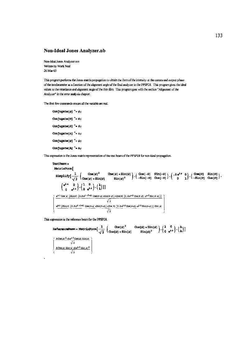
133
Non-Ideal Jones Analyzer.nb
Non-Ideal Jones Analyzer.nm
Witten by Mark Neal
26 Mar 03
This progwnperfonTB the Jones rratrixpropagption to obtain the forniof the intensity at the camera and output phase
of the inteferometer as a functiwi of the aligiment an^e of the final analyzer in the PPSPDI. This progwn gives the ideal
values to the retandance and aligitiHit an^e of the tWn film This progmn gDes with the section "Aligurent of the
Analyzer" in the error analysis ch^ter.
The first few cxsnrands ensure all the variable are real.
Oonjugat»[^]
Ocnjugate[e] *=6;
Conjugate [<S] *= 6;
OQnjtigate[A] A;
Ocnjugat»[(^] *=
CcnjugataEA] *= A;
This ejipression is the Jones matrix representatiai of the test beam of the PPSPDI for non-ideal prqia^ion.
Test:Beam =
MatrlxFaim[
SlTOlifv-r— ( aos[i(r]. Sinew \ / Oos[-e] Sln[-e]\ (.8e** 0\ / aca[e] Sln[e]» Kfi ' Oos[|^] *Sln(|^l Sin[|^]^ j'Usin[-e] ac5s[-e]r( o lj'Usin[e] C08[e] )'
ei'^03s[»l (siniei (o.Be^Cbsie-»|tSln[e-i>l)-tCt]s|ei (o.8e^'*tt)6[e-i>i-e^'^Sln[e-ii<l)) '
(slniei (0.8ei 03B[9-!>] <-Sln[e-»l )-fCCsie] (o.8e^'*03s[9-»l-e^'5siii|e-i»l)) Slii[»l
V 2
This expression is the reference beam for the PPSPDI.
KeferenceBeeon =s HatrixForm[—^ 1 I aos[((f]^ Ctos[i^]*Sl
^"2 loosEW *Sin[i<f] Sin[ifr]
Cbs[|fr] *Sln[)^] 2 )•(;
AO06[</f)^+Ae^*^Cb6[i/fl Sin[i/f] "j
AQpel i / f ] Sin[i^]4-Ae^^Sin[i/f]^
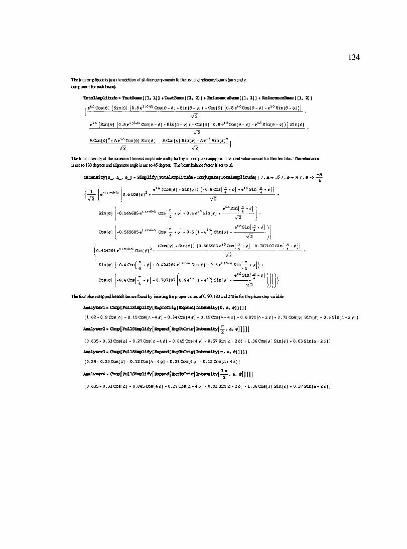
134
The tc^al anplitude is just the addition of all four oonponents fo the test and reference beams (an x and y
conpcmoit for eadi bean^.
TotalAnplltude s TestBeam[[l, 1]] +TestSeam[[l, 2]] •«- ReferenceBeam [ [1, 1}] * Refer€DcdBeam[[l, 2]]
( S i n [ e ] ( 0 . 8 C o s [ e - i/ f ] + S i n [ e - i / f ] ) + C o s [ 0 ] ( 0 . 8 e ^ ' ^ C o s [ e - S i n [ e - i ^ ] ) )
e''' (Sin[e] (0.8 Cos[e- i^] +Sin[e- ij/]) + Cos[e] (0.8 e'*Cos[e - lA) - e*''Sin[e - lA])) Sin[i;()
ACos[«J^ + Ae'''Cos[iA] Sin[i>] ACos[i/(] Sin[i/;] + Ae'''Sin[i/(]^
The total intensity at the catiera is the total anplitude niiltiplied by its conplex conjure. The ideal values ate set for the thin film The retardance
is set to ISOdegeesandaligiment an^eisset to45degiees. Thebeambalancefktorisset to.6.
liitensity[6_, A_, ((rJ = Sinpli£y[TotaUiiplitu<Sa*Oonjijgate(TotalSiiplituda]] /.A-» .6 /. TT /. e-> — 4
e''^ (Cos[if] +Sin[i(/]) (-0.8Cos[-^ -n^] +e'''sin[^ + li'])
0.6Cos[iA]^ + * V2
I r 71 1 e^ 'Sinf — +1^1 ' Sin[iH -0.565685 6'""^®"^'Cos —+<(< +0.6e"^Sin[ i / (J + *
IT »j'^Sin[— + i/fl iCttS+a) " ^,,,1 n , M - - Id J
C o s [ i / f ] - 0 . 5 6 5 6 8 5 C 3 o s — + i/ ( + 0 . 6 ( l + e ) S i n [ i J ( ] ^ L 4 J > ' ^
{Cos[lA) +Sin[l(']) (0.565685 e*''Cos [-J + If] - 0 .707107 Sin [-J + i^])
sin[ i (r ] (-0.4 0os[— + i / f ] + 0.424264 e* Sin[iH + 0.5 6""*® Sin[— + ) +
e^Sinf^-Cos[i;fl I-0.4 Cios[—+ i/fj-0.707107 0.6c'^ (1 + c") Sin[i//] + -
The four phase stepped intensitites are found by insetting the pix:^^ values of0,90,180 and 270 in fo* the phase stq> variable
Analyzerls Ghop[S\3llSiiipllfy[E39ToTrig[E}qpand[£atesisity[0/ A,
{1.02 + 0.9 Cos [A] - 0.15 Cos[A - 4 - 0.34 Cos [4 i j / ] - 0.15 Cos [A + 4 i / f ] - 0.6 Sin[A - 2 i / f ] + 2.72 Cos[i/'] Sin[</f ] + 0.6 Sin[A + 2i i f ] }
Aiialyzer2« ChQS)[FullSiiqpllfy[E:9and[Biq;/roTrlg[llitenslty-[y / A, t^]]]]]
{0.635+0.33 Cos[A] - 0.27Cos[A -4 (//] - 0.045Cos[4 i / f ] - 0.57 Sin[A-2 i / f ] +1.36Cos[iA] Sin[ i l / ] + 0.03 Sin[A+2 t / f ]}
AnalyaerS• Chcp[FallSiBplify[B>qpand[ayHWadg[lfateP8i^[TT , l,
{0.25-0.24 Cos[A] -0.12Cos[A-4iA] + 0.25 Cos[4 lA] - 0.12 CostA+4 </^]}
Axialyzer4 » C3]cp[FullSi3iplify[Bxpaiid[&iqxreyrrig[lbteaslty['^^, A, <^]]]]]
{0.635+ 0.33 Cos[A] - 0.045Cos{4 </f] - 0.27 Cos[A + 4 i / r ] - 0.03 Sin[A- 2 l i^] + 1.36 Cos[( / f ] Sin[ ip ] + 0.57 Sin[A+2 i / f ]}

135
The four intensities are then put into a four step phase shifting algxithm to calculate the output phase from the interferometa-
as a fiinction of the an^e of the analyzer and the input phase from the test optic. This is the equation used in the IDL pn^^
to find the error in the output of the interferorreta.
AnalyzerPhase = ArcTan[Sijipllfy[
{ArcTan[ (0.27 Cos [A - 4 i/f] - 0.27 Cos[A + 41//] + 1.08 Cos [2 i/*) Sin[Al) / (0.77 + 1.14 Cos[A] -
0.03 Cos[ A - 4iA] - 0.59 Cos [4 t ] - 0.03 Cos [ A + 4i l i ] - 0.6 Sin[ A - 2 lA) + 2.72Cos[i/f] Sin[)/(] + 0.6 SinlA+ 2i l i ] ) ] )
This plots the four intensities as a fiinction of input phase from the test optic for the ideal case with the analyzer aligied
atOd^iees.
Flot[ {Analyzerl /. i/r-« 0, Analyz6r2 /. 0, Analyzers /. 0, Analyzer4 / . i l i -» 0 ) , {A, 0, 2 TT ) , PlotStyle-» {{RGBOolorll, 0, 0]}, {BGB0olor[0, .5, 0]}, {RGBaolor[0, 0, 1]}, {R3BC3olor[.5, .5, .5])), ftxesIiabel-> (Surface Phase A, Intensity}]
Intensity
1.2
1
0 .8
0.6
0.4
0.2
Etiase Surface A 1 2 3 4 5 6

136
analyzererrorl SO.pro
pro analyzererrorl 80
jWritten by Mark Neal on 26 Mar 03
;This program calculates the error due to the final analyzer being at the wrong angle in the PPSPDI ;and includes diattenuation in the film. It is assumed that the film has 180 degrees retardance and is ;oriented at -45 degrees. The analytic solution was obtained using a ;Mathematica program with the filename "Non-Ideal Jones Analyzer.nb"
;Define the arrays used. device, decompose=0 k=100 num=fltarr(k) denom=fltarr(k) phase=fltarr(k) difference=fltarr(k) Ideal=fltarr(k) delta=fltarr(k) i=conq)lex(0,l) surf=fltarr(k) theta=fltarr(k) maxx=fltarr(k) minn=fltarr(k) error=fltarr(k) stddeviat=fltarr(k)
;Loop through the different analyzer angles for m=0,k-l do begin theta(m)=double(-9.3+. 1 *m)*(!pi/180.0)
;Loop through the input surface phase from 0 to 2pi. If perfect then the output of the program will ;be exactly this value for n=0,k-l do begin surf(n)=double((2.0* !pi*(n))/k)
;This is the analytic solution from Mathematica for 14-12. num(n)=.27'''Cos(surfl[n)-4*theta(m))-.27*Cos(surfl[n)+4*theta(m))+1.08*Cos(2*theta(m))*Sin(surf(n))
;This is the analytic solution fi-om Mathematica for 11-13. denom(n)=.77+l. 14*Cos(surf(n))-.03*Cos(surf(n)-4'''theta(m))$ -.59*Cos(4*theta(m))-.03*Cos(surf(n)+4*theta(m))$ -.6*Sin(siu^n)-2'''theta(m))+2.72*Cos(theta(m))*Sin(theta(m))+.6*Sin(siu'f(n)+2*theta(m))
;This calculates the phase -> ArcTan((I4-I2)/(Il-I3)) phase(n)=Atan(num(n)/denom(n))
endfor
;Plot the wrapped output phase and input phase window, 1

137
plot,surf,phase,Background=255,color=0,title-Measured Phase vs. Input Phase',$ xtitle-input phase',ytitle-Measured Phase' oplot,surf,atan(tan(surf)),color=0
;Unwrap the output phase to remove the phase ambiguities. for n=0,98 do begin if (phase(n) gt 0.0) and (phase(n+l) gt 0.0) and (phase(n+l) gt phase(n))$ and (abs(abs(phase(n+l))-abs(phase(n))) gt .8) then phase(n+l:*)=phase(n+l:*)-!pi if (phase(n) gt 0.0) and (phase(n+l) gt 0.0) and (phase(n+l) le phase(n))$ and (abs(abs(phase(n+l))-abs(phase(n))) gt .8) then phase(n+l:*)=phase(n+l:*)+!pi if (phase(n) gt 0.0) and (phase(n+l) le 0.0) and (abs(abs(phase(n+l))+phase(n)) gt .8)$ then phase(n+l :''')=phase(n+l :*)+!pi if (phase(n) le 0.0) and (phase(n+l) gt 0.0) and (abs(phase(n+l)+abs(phase(n))) gt .8)$ then phase(n+l ;''')=phase(n+l ;''')-!pi if (phase(n) le 0.0) and (phase(n+l) le 0.0) and (phase(n+l) gt phase(n))$ and (abs(abs(phase(n+l))-abs(phase(n))) gt .8) thenphase(n+l:''')=phase(n+l:''')-!pi if (phase(n) le 0.0) and (phase(n+l) le 0.0) and (phase(n+l) le phase(n))$ and (abs(abs(phase(n+l))-abs(phase(n))) gt .8) thenphase(n+l:*)=phase(n+l:*)+!pi endfor
;Plot the unwrapped output and input phase. window,! plot,surf,phase,Background=255,color=0,title-Measured Phase vs. Input Phase',$ xtitle-Input Phase',ytitle-Measured Phase' oplot,surf,surf,color=0
;Calculate and plot the difference between the output and input phase from the surface. difference=phase-surf window,3 plot,surf,difference,background=255,color=0,title='Difiference Between Measured Phase and Input Phase',$ ytitle-Phase Difference',xtitle-Input Phase'
;Find the maximum, minimum, max-min and standard deviation for the difference of the input and output phase. maxx(m)=max(difference) minn(m)=min(difference) error(m)=maxx(m)-minn(m) stddeviat(m)=stddev(diflference,/double,/nan) ;Print the peak to valley and rms error in waves for each value of analyzer angle. print,(180/!pi)'''theta(m),' peak to peak error in waves ',error(m) print,(180/!pi)'''theta(m),' rms error in waves ',(l/(2*!pi))*stddeviat(m) endfor
;Plot the peak to valley and rms error in waves vs. analyzer angle. window,4 plot,(180/!pi)*theta,abs(error),background=255,color=0,title-Peak to Valley Error vs. Analyzer Angle',$ xtitle-Analyzer Angle',ytitle='Peak-to-Valley Error (in waves)' window,5 plot,( 180/!pi)*theta,( 1/(2"' !pi))*abs(stddeviat),background=255,color=0,title='RMS Phase ErrorS vs.Analyzer Angle',xtitle-Analyzer Angle',ytitle='RMS Error (in waves)
end

138
Non-Ideal Jones Retardance for 160.nb
Non-Ideal Jones Retardance for 160.nb
Wntten by Mark Neal
26 Mar 03
This programperfcams the Jones matrix propa^ion to obtain the intensity at the camoa and output phase of the interferomster
for a thin film with a retardance of 160 d^iees like the one actually used in the PPSPDI. This progwn sets the an^e of the retarder
and an^eoftheiinal analyzer to their ideal values. Thisprogramg)es with the section "Actual PPSPDI Film with 160 D^g^
Retardance" in the aior analysis ch^ta.
The first few commands ensure that all the variables are real.
« Gc£^ihlcs~Legancl~
aonjugate[0]
C3Qnjugat»[©] ''s 6;
Oanjugate[£] 6;
aciijugate[A] A;
C3onjugat»[(>f] iln
aanj\]gat:e[A] A;
This egression is the Jones matrix represaitation for the test beam of the PPSPDI given in the error analysis ch^ter. Values for the
variables have not been set.
TestBeam =
Matri:fbzin[
V Cos[i(f] *SinW Sin[i(r]2 ] \-Sin[-e] (X>s[ - e ] I \ o 1/
/ Cos[e] Since] ^ ° ° ^ i^\U I-Since] O o a i e ] l ' [ q
' e^^oxlili] (sin[ei (o.8e^Cl36[9-i^] 4-Sm[e-iffl )-i-CbB[ei (o.8e^'<'036[e-i<']-e^'Ssui[9-iAl))
^|2
(sin[e] (o.8e^ Cbs[e-»] <-Sin[e-i/f] )-fCfc6[9] (o.8e^'*'036[e-i/>l-e^'Ssin[e-!^])) Sin[^l
V2
This is the egression for the reference beam for the PPSPDI.
Refer^^-»^tri^nn[^*( aosW*SinW^ (l 0^ VCos[l/f] *Sin[i(r] Siii[t/r]2 } U e*®/ \A/J
AOos[t / f ]^+Ae^'^Oo6lJA] Sin[ i j f ]
V2
ACtB[»] Sialyl -t-Ae^ Sinli/f]
V2

139
The total anplitude is just the addition of all four cxntponents of the test and reference beams (an x and y
component fcH- each beam).
TotaUnpUtude = TestSeain[[l, 1]] +TestBeam[ [1, 2]] + Ke£erenceBeam[ [1, 1]] + Re£er<enc^Beam[ [1, 2]]
,e^'^Cos[iA] (sin[e] (0.8 Cos[e - lA] + Sin[e - lA]) + Cos[e] (0.8e''''Cos[e - i/r) -e*''Sin[e - lAl))
f vi (Sin[e] (0.8 c'Cos [e-iA] +Sin[e-iAl) +Cos[0] ( 0 . 8 e ^ ^ C o s L e - l A l - S i n [e - lA])) Sin[iAl _ ,
ACos[i/fl^ +Ae^''Cos[iA] Sin[(Al ACos[iA] Sin[(A) + Ae^''Sin[iA]^ i
42 42 •'
The total intensity at the camera is the total amplitude nultiplied by its complex conjure. The ideal values for the aligiment an^es of the analyzer
and thin filmare set to Od^iees and-45 d^rees respectively. Thebeambalanceikaoris set to .6. The retardanceofthe film is still left as
a variable.
Retardancelnten8lty[<5_, A_, <)>_} =
Chop [ ExpTtfTid^ [ E]^«i)d [ TotalAnplltucle * Ocnjugat^e [Totalftnplitude] ]]] /.A-» .6/.e->^ /.((f-»0 4
{0.59+ 0.09Cos[5] + 0.3Cos[A] + 0.3 Cos[(5 + A] +
0 . 2 C o s [ ( 5 - 0 1 - 0 . 2 C o s [ 6 + 0 ] + 0 . 2 4 C O S [ A + tp] - 0 .24 Cos [5 + A + 0])
This is the intensity with the retardanceofthe film set to 160d^«es.
Intensity = (3]pp[FullSiiiplify[netai:danceIntensity[5, A, ~^^]]]
{0.59+0.09Cos[6] + 0.0744738 Cos [A] +
0.525526 Cos[6+A] + 0.136808 Sin[51 - 0.0820848 Sin[A] + 0.0820848 Sin{6 + A]}
This is a plot of the four phase stepped intensities usingphase shift values of0,90,180 and 270. From the plot it can be seen
that these shifts do not shift the intensities by 90 degiees.
Plot[{KetarclanceIntenslty[0, A, ]' R8tardancellitensity[-^ , A,
. , 160 TT, , .^,37r ITT 160 x ,, „ „ Setaz(3ancelntenslty[7r, A, ], RetardanoeIntensity[-^ +, A, ]}, {A, 0, 2 7r},
AicesStyle-^ Thickness [ .004],
PlotStyle-» {{Absolute!nilclaiess[2], SGBOolor[l, 0, 0]},
{Absolut^lhlc]a)ess[2], Dashing[{.015, .015}], KGBCblor[0, .5, 0]},
(Absolut^Ihlc]aiess[2], Dashij]g[{.02S, .025}], KGB0olor[0, 0, 1]},
{Absolut^Ihlckness[2], Dashli)g[{ .05, .05}], KGBaolor[.5, .5, .5]}},
taasLabel-* {"Surface Riase A", "liitenaity"}, PlotLegend-» {"0°", "90°", "180°", "270°"},
LegendPosltlon-* {.65, -.3}, LegendSlze-* {.6, .6}, LegendShadcw-• None]

Intensity
1.2
0 .8
0 .6
0.2
1 2 3 4 5 6
Two intaisities can be plotted ag3iiist each other to see at what phase shift value the intoisities are 90 deg^
out of phase. For this plot the first and fourth steps are plotted and show that the correct shift for the
fourth intaisity is 271 d^pes. The second and third intensities can be sa the same way.
r r , . r 160 TT , , , , 3 TT 1 Tt 160 TX ^ , Plot [ I RetaroancelntPinflity[ 0, A, J, Retaraancelnt^ensity[ J},
{A, 0, 47r}, PlotStyle-» {{RGBCtolor[l, 0, 0]}, {RGBOolcMr[0, .5, 0]}}, r r f 3 TT _ 5 TT _ 7 TT , . , ,
GridLlnes-> ti"^' ^ ^ }' Autcoiat:xc|J
0.8-
0.6-
0.4-
0.2-\
The four correctly phase stepped intensities are found by insating the propa phase stq)s of0,97,198 and 270 degrees
into the intensity equation with the retardalK® of the film set to 160 deg'ees. This gives foiff intensities as a fimction
of the input phase fixjm the test lens only.
Retardancel = Chop[Sinplify[Retarrlancelntennity[0, A, 160 TT
180 ] ] ]
{ 0 . 6 8 + 0 . 6 C o s [A] )
Retardance2 = Cbop[Sinpli^[RetardanceTnt:ensity[-^ + " , A, " ] ] ] 2 180 180
( o . 694517+ 0.0870344 Cos [A] + 0.3Cos[ + A ] - 0.321756 Sin[A] 1 L ^ 180 J J
Setardance3 = Cbop[Siiipllfy[Betazt5anceIatenslty[7r+ , A , — ] ] 180
{ o . 462129- 0.210843 Cos [A] - 0.24 Cos[ " + A ] + 0.0106203 Sin[A] |
Itetardar>ce4 = a«^[Sii.pUfy[Ret^rdaiK:eIiiten^^^ ^]]]
f o . 454783+ 0.0744738 Cos [A] + 0.3 Cosf + AI - 0.24 Cos[ + AI - 0.0820848 Sin[A] | I L ifto J L 180 J J

This plots the four intensities for comparison.
Plot[{Ret-aniancel, Retai:dance2, Setardance3, Retaxdance4}, {A, 0, 4 7r},
I • t t i l l GcidLliies-» . 3 TT, Autcmaticj j
1.2
0.8-
O.fr
0.4- -
0.2-
The next several lines find the tnaxinum and inininMn values of the four intensities referred to as fiames. These will be used
lata to contrast stretch the intensities.
Ei:ainal= Table[0.68'+0.599999aos[A], {A, 0 720 1 °)];
inaxl^ UaxEFraniel]
1.28
mini: Ifin[Fi:2Diel]
0.080001
Fram02 = Table [ 0.6945167 + 0.0870344 Oos [A] + 0.2999999 Ctos [ + A] - 0.3217559 Slu [ A], 180
{A, 0®, 720 ° , 1 ° ) ] ;
inax2 = lto[Fi:aine2]
1.30316
iiiln2 = lIln[Frame2]
0.0858695
ft'aine3 = T^le[0.4621288-0.2108431GOS[A] - 0.2399999OO S + A ] + 0.0106202 Sin[A] ,
{A, 0% 720°, 1°)];
inaxS = Maic[Ei:aine3]
0.912826
inin3 = Itln[Ki:anie3]
0.011432
Fteone4 = Table [0.4547834 + 0.0744737 Cos [A] + 0.2999999 Oos +A] - 0.2399999 Ctos[-^^^
0.0820848 Sin [A], {A, 0°, 720°, 1°)];
iiiax4 = lfax[Frains4]
0.899577
iidii4 = Min[Fi:an)e4]
0.00998963

142
This is a plot of the first frame after contrast stretching
E^ranel - mini, LlstPlot[-
maxl - mini
100 200 300 400 500 600 700
- Graphics -
These are the four intensities after contrast stretching
Setardancel - mini Ketaxwoicel =
maxl- mini
{0.833335 (0.599999+ 0.6COS[ A ] ) }
Rstard»ice2 - min2 I!et:ardance2 =
max2 - min2
{o.821494 (0.608647+ 0.0870344 Cos[&] +0.3Cos[
SetardanceS - min3
107 71
180 + A - 0.321756
Retardance3= maxS- mln3
|l.10939 (0.450697- 0.210843 Cos [ A ] - 0.24 Cos[
Ketardance4 - min4
179 71
90 - A + 0.0106203
Sin[ A ] ) ]
Sin[ A ] ) }
I!etai:dance4 = m!Dc4- min4
|l.12412 ( 0 .444794+ 0.0744738 Cos[ A ] + 0.3Cos[^^ + A ] - 0.24 Cos 43171
180 - 0.0820848 Sin[ A ] ] J
The next two commands plot the contrast and properly phase shifted intensities to compare with the plot of the four intoisities
before the correct phase stq)s and contrast stretdiinghave been plied.
$De£eniltPtont = {"Arial", 13}
{Arial, 13}
Flot[{Ret:axdancel, Retardance2, RetiardanceS, Ret:axd2aice4}, {A, 0, 2 7r}, AxesStyle-> Thickness[.004],
P lo t :S ty l e -> {{Abso lu t eTh lcknes s [2 ] , I ! imao lo r [ l , 0 , 0]} ,
{Absolut^Ihlclcaess[2], Dashlng[{ .015, .015}], SGB03lar[0, .5, 0]},
{Absolut^Itaickness[2], Dashing[{ .025, .025}], RGBaolor[0, 0, 1]}, {Absolut:e!n>lc]aiess[2], Dashln9[(.05, .05}], KG8Cblar[.5, .5, .5]}},
Axedijabel-^ {"Surface Phase A", "Intensity"}, PlotLegei]d-» {"Xi", "Ij", "I3", "I4"}, LegendPosltlan-» {.55,-.3}, LegendSlze-> {.6, .6}, LegendShadow-* Nbne]

143
Intensity
0.8
0.6
0.4
0.2
Surface Phase A 1 2 3 4 5 6
The four intensities are then put into a four step phase shifting routine to calculate the output phase from the interferometer
as a function of the input phase fixjm the test lens. So, the difference between the output phase and input phase can be caclulated.
RetardancePhase = Chcp[Sii,plify[ArCI^[ 11 ] •• •• Chop[SlnpIi£y[Retardancel-RBtan3ance3], 10-^]
|ArcTan|
0.012219COSTA] - 0.246448Cos[^5ZII + o .337235Cos[+ AI - 0.269788Co s [ + a ] + 0.172048Sin[A] 180 ' 180 ' I- 180 '
0.733909 Cos[A] + 0.266254 COS[-I^ + A] - 0.011782 Sin[A]
]}
This is aplot of both the input and output phase. Thsy are very close to the same.
Plot[(RetariiancePhase, Aix;ran[Tan[/^] ]}, {A, 0, 2n)]
0.5
-0.5
-1.5
This is aplot of the difference between the input and output phase for input phase values from 0 to 2i^. The vertical scale is in
radians.
Plot[KetardancePhase-ArCTan[Tan[A]], {A, 0, 2n)]
0.0025
0.0024
0.0023
0.0022

144
errorfor 160plate.pro
pro errorfor 160plate
;Written by Mark Neal on 26 Mar 03
;This program calculates the error due to the retardance of the fihn being 160 degrees. This simulation ;includes diattenuation in the film. It assimies a retardance of 160 degrees with the film oriented at -45 ;degrees. The analyzer angle is set to 0 degrees. The analytic solution was obtained using a ;Mathematica program with the filename "Non-Ideal Jones Retardance for 160.nb"
;Define the arrays used. device, decompose=0 k=100 num=fltarr(k) denom=fltarr(k) phase=fltarr(k) diflFerence=fltarr(k) Ideal=fltarr(k) delta=fltarr(k) i=complex(0,l) surf=fltarr(k)
;Loop through the input surface phase fi-om 0 to 2pi. If perfect then the output of the program will ;be exactly this value for n=0,k-l do begin surf(n)=double((2.0* !pi*(n))/k)
;This is the analytic solution from Mathematica for 14-12. num(n)=.012219*Cos(surf(n))-.246448*Cos((( 107* !pi)/180)+surf(n))+$ .337235*Cos(((271»!pi)/180)+surf(n))-.269788*Cos(((431*!pi)/180)+surf(n))$ +.172048*Sin(surf(n))
;This is the analytic solution from Mathematica for 11-13. denom(n)=.733909*Cos(surf(n))+.266254*Cos(((179*!pi)/90)+siu:f(n))-.011782*Sin(surf(n))
;This calculates the phase -> ArcTan((I4-I2)/(Il-I3)) phase(n)=Atan(num(n)/denom(n))
endfor
;Plot the wrapped output phase and input phase window,! plot,surf,phase,Backgroxmd=255,color=0,title-Measured Phase vs. Input Phase',$ xtitle-input phase'.ytitle-Measured Phase' oplot,surf,atan(tan(surf)),color=0
;Unwrap the output phase to remove the phase ambiguities. for n=0,98 do begin if (phase(n) gt 0.0) and (phase(n+l) gt 0.0) and (phase(n+l) gt phase(n))$ and (abs(abs(phase(n+l))-abs(phase(n))) gt .8) thenphase(n+l:*)=phase(n+l:*)-!pi if (phase(n) gt 0.0) and (phase(n+l) gt 0.0) and (phase(n+l) le phase(n))$

145
and (abs(abs(phase(n+l))-abs(phase(n))) gt .8) then phase(n+l:*)=phase(n+l:*)+!pi if (phase(n) gt 0.0) and (phase(n+l) le 0.0) and (abs(abs(phase(n+l))+phase(n)) gt .8)$ then phase(n+l :*)=phase(n+l :*)+!pi if (phase(n) le 0.0) and (phase(n+l) gt 0.0) and (abs(phase(n+l)+abs(phase(n))) gt .8)$ then phase(n+1: *)=phase(n+1: *)- !pi if (phase(n) le 0.0) and (phase(n+l) le 0.0) and (phase(n+l) gt phase(n))$ and (abs(abs(phase(n+l))-abs(phase(n))) gt .8) thenphase(n+l:*)=phase(n+l:*)-!pi if (phase(n) le 0.0) and (phase(n+l) le 0.0) and (phase(n+l) le phase(n))$ and (abs(abs(phase(n+l))-abs(phase(n))) gt .8) thenphase(n+l:*)=phase(n+l;*)+!pi endfor
;Plot the unwrapped output and input phase. window,2 plot,surf,phase,Background=255,color=0,title-Measured Phase vs. Input Phase',$ xtitle-Input Phase',ytitle-Measured Phase' oplot,surf,surf,color=0
;Calculate and plot the difference between the output and input phase from the surface in waves. difference=(l/(2*!pi))*(phase-surf) window,3 plot,surf,difference,/ynozero,pos=[.20, 0.1, .95, .9],background=255,color=0,title='Difference Between Measured Phase and Input Phase',$ ytitle-Phase Difference (in waves)',xtitle-Input Phase'
;Find the maximiun, minimiun, max-min and standard deviation for the difference of the input and output phase. maxx=max(difference) minn=min(difference) error=maxx-minn stddeviat=stddev(diflFerence,/double,/nan) ;Print the peak to valley and rms error in waves for each value of analyzer angle. print,maxx print,minn print,'peak to peak error in waves',error print,'rms error in waves ',stddeviat
end

146
referencewavequality.pro
pro referencewavequality device, decompose=0
jWritten by Mark Neal on 26 Mar 03
;This program is used to investigate the quality of the reference wave in a PDI ;as a fimction of pinhole size and aberrations on the incident wave. The program allows the ;person using it to vary the incident aberrations and the size of the pinhole. This way, all aberrations ;and pinhole sizes can be investigated. The phase and amplitude of the beam is calculated at the plane ;prior to the pinhole and in the final image plane. So, the phase and amplitude at the pinhole, size of the :pinhole and error in the reference wave can be correlated together.
;Sets the array sizes ObjectEdge=2048 LensFunction=complexarr(ObjectEdge,ObjectEdge) Wtotal=complexarr(ObjectEdge,ObjectEdge) Aberration=con:q)lexarr(Obj ectEdge,Obj ectEdge) Transform=complexarr(ObjectEdge,ObjectEdge) TransformPhase=complexarr(ObjectEdge,ObjectEdge) AfterPDI=complexarr(Obj ectEdge,Obj ectEdge) cylinder 1 =fltarr(ObjectEdge,Obj ectEdge) cylinder2=fltarr(0bjectEdge,0bjectEdge) cylinder3=fltarr(0bjectEdge,0bjectEdge) PDIpinhole=fltarr(objectEdge,ObjectEdge) FinalImage=con:q)lexarr(ObjectEdge,ObjectEdge) FinalPhase=fltarr(ObjectEdge,ObjectEdge) PerfectLens=fltarr(ObjectEdge,ObjectEdge) PerfectTransform=fltarr(ObjectEdge,ObjectEdge) BigPinhole=fltarr(ObjectEdge,ObjectEdge) PerfectImage=fltarr(ObjectEdge,ObjectEdge) PerfectPhase=fltarr(ObjectEdge,ObjectEdge) i=con5)lex(0,1.0) lambda=632.8E-9 k=2*!pi/lambda
;Sets the cylinder function for the lens function radius=64 LensFunction=dist(ObjectEdge,ObjectEdge) LensFunction=shift(LensFunction,ObjectEdge/2,ObjectEdge/2) index=where(LensFunction le radius) LensFunction(index)=1.0 index=where(LensFimction gt radius) LensFimction(index)=0.0
;Define the aberration values (put various values in here - in waves). W200=0.0 W l l 1 = 0 . 0 W020=0.0 W040=0.0 W131=0.0

147
W222=0.0 W220=0.0 W311=0.0
;Create the aberration function for n=0,2*radius-l do begin xpupil=l .0*(n-radius)/radius x=0bjectEdge/2-radius+n
for j=0,2*radius-l do begin ypupil=l .0*(j-radius)/radius y=0bjectEdge/2-radius+j
Wtotal(x,y)=W200+Wlll*ypupil+W020*(xpupil''2+ypupil''2)+W040*((xpupil''2+ypupil^2)^2)$ +W131 *(xpupil'^2+ypupil^2)'''ypupil+(W222*(ypupil''2))+W220*(xpupil'^2+ypupil'^2)+W311 *ypupil
endfor endfor
index=where(LensFunction eq 1.0) Aberration(index)=Exp(i*2*!pi*Wtotal(index))
LensPhase=fltarr(ObjectEdge,ObjectEdge) imaginarypart=imaginary(Aberration) realpart=float(Aberration) LensPhase=Atan(iniaginarypart,realpart) window, 1 plot,LensPhase(0:ObjectEdge-l,ObjectEdge/2),background=255,color=0,title-Horizontal Test Lens Phase' window,2 plot,LensPhase(ObjectEdge/2,0:ObjectEdge-l),background=255,color=0,title-Vertical Test Lens Phase'
;Fourier Transforms the Aberration Function to propagate to focus Transform=FFT(shift(Aberration,ObjectEdge/2,ObjectEdge/2),-l) Transform=shift(Transform,ObjectEdge/2,ObjectEdge/2) Window,4 plot,Transform(ObjectEdge/2-100:ObjectEdge/2+100,ObjectEdge/2),$ pos=[.15, 0.1, .95, .9],background=255,color=0,title-X Profile of FFT at the Pinhole',$ xtitle-X position (pixels)',ytitle-Amplitude' Window,5 plot,Transform(ObjectEdge/2,ObjectEdge/2-100:ObjectEdge/2+100),$ pos=[.15, 0.1, .95, .9],background=255,color=0,title-Y Profile of FFT at the Pinhole',$ xtitle-Y position (pixels)',ytitle-Amplitude'
TransformPhase=(l/(2*!pi))'''Atan(Imaginary(Transform),Float(Transform)) window,6 plot,TransformPhase(ObjectEdge/2-100:ObjectEdge/2+100,ObjectEdge/2),$ background=255,color=0,title-X Profile Phase at the Pinhole' window,? plot,TransformPhase(ObjectEdge/2,ObjectEdge/2-100:ObjectEdge/2+100),$ background=255,color=0,title-Y Profile Phase at the Pinhole'
;Phase Unwrap the Phase at the Pinhole Over a Region Approximately 5 Times the Diameter of the Pinhole htransformphase=fltarr(200)

148
htransformphase=TransformPhase(ObjectEdge/2-100:ObjectEdge/2+100,ObjectEdge/2) imtialcenter=htransfonnphase( 100) for n=0,199 do begin if (htransformphase(n) gt 0.0) and (htransforaiphase(n+l) gt 0.0) and (htransformphase(n+l)$
gt htransfomphase(n)) and (abs(abs(htransformphase(n+l))-abs(htransfomq)hase(n))) gt .6) $ then htransformphase(n+1: *)=htransfomiphase(n+1: *)-1.0
if (htransformphase(n) gt 0.0) and (htransformphase(n+l) gt 0.0) and (htransfonnphase(n+l)$ le htransfom^hase(n)) and (abs(abs(htransformphase(n+l))-abs(htransformphase(n))) gt .6)$ then htransformphase(n+1: *)=htransfonnphase(n+1: *)+1.0
if (htransfomiphase(n) gt 0.0) and (htransformphase(n+l) le 0.0) and$ (abs(abs(htransfom:q)hase(n+l))+htransfomiphase(n)) gt .6)$ then htransformphase(n+1: *)=htransfomiphase(n+1: *)+1.0
if (htransfomphaseCn) le 0.0) and (htransformphase(n+l) gt 0.0) and$ (abs(htransfonnphase(n+l)+abs(htransformphase(n))) gt .6)$ then htransformphase(n+1: *)=htransfonnphase(n+1: *)-1.0
if (htransfonnphase(n) le 0.0) and (htransfomiphase(n+l) le 0.0) and (htransformphase(n+l)$ gt htransfomphase(n)) and (abs(abs(htransformphase(n+l))-abs(htransformphase(n))) gt .6)$ then htransformphase(n+1: *)=htransformphase(n+1: *)-1.0
if (htransfonnphase(n) le 0.0) and (htransfomiphase(n+l) le 0.0) and (htransfonnphase(n+l)$ le htransfomiphase(n)) and (abs(abs(htransformphase(n+l))-abs(htransformphase(n))) gt .6)$ then htransfom:5)hase(n+1: *)=htransfomiphase(n+1: *)+1.0
endfor finalcenter=htransformphase( 100) difference=finalcenter-initialcenter htransfomiphase=htransformphase-difference window,8 plot,htransformphase,background=255,color=0,title-X Profile Phase at the Pinhole',$ xtitle-X position (pixels)',ytitle='Phase (waves)'
vtransformphase=fltarr(200) vtransformphase=TransfonnPhase(ObjectEdge/2,ObjectEdge/2-100:ObjectEdge/2+100) initialcenter=vtransfonnphase( 100) for n=0,199 do begin if (vtransfomq)hase(n) gt 0.0) and (vtransfonnphase(n+l) gt 0.0) and (vtransformphase(n+l)$
gt vtransformphase(n)) and (abs(abs(vtransformphase(n+l))-abs(vtransfoni5)hase(n))) gt .8)$ then vtransfomiphase(n+1: ''')=vtransformphase(n+1: •")-1.0
if (vtransformphase(n) gt 0.0) and (vtransformphase(n+l) gt 0.0) and (vtransformphase(n+l)$ le vtransfomiphase(n)) and (abs(abs(vtransformphase(n+l))-abs(vtransformphase(n))) gt .8)$ then vtransfomiphase(n+l :''')=vtransformphase(n+l :*)+l .0
if (vtransformphase(n) gt 0.0) and (vtransfomiphase(n+l) le 0.0) and$ (abs(abs(vtransfonnphase(n+l))+vtransfomiphase(n)) gt .8)$ then vtransfomq)hase(n+1: ''')=vtransfom5)hase(n+1: *)+1.0
if (vtransformphase(n) le 0.0) and (vtransfoni^hase(n+l) gt 0.0) and$ (abs{vtransformphase(n+l)+abs(vtransformphase(n))) gt .8)$ then vtransformphase(n+1: *)=vtransfoni^hase(n+1: *)-1.0
if (vtransfoni^hase(n) le 0.0) and (vtransformphase(n+l) le 0.0) and (vtransformphase(n+l)$ gt vtransforn:^)hase(n)) and (abs(abs(vtransfomiphase(n+l))-abs(vtransformphase(n))) gt .8)$ then vtransformphase(n+1: *)=vtransformphase(n+1: *)-1.0
if (vtransformphase(n) le 0.0) and (vtransformphase(n+l) le 0.0) and (vtransformphase(n+l)$ le vtransfom^hase(n)) and (abs(abs(vtransfonnphase(n+l))-abs(vtransfonnphase(n))) gt .8)$ then vtransformphase(n+1: ''')=vtransformphase(n+1: *)+1.0
endfor finalcenter==vtransfomiphase( 100)

149
difFerence=fmalcenter-initialcenter vtransfoniiphase=vtransformphase-difference window,9 plot,vtransfomiphase,backgroimd=255,color=0,title-Y Profile Phase at the Pinhole',xtitle-Y position (pixels)',ytitle-Phase (waves)'
;create cylinder function for PDI pinhole ;pinholeradius=4 for 25% of the Airy disk ;pinholeradius=9 for 50% of the Airy disk ;pinholeradius=14 for 75% of the Airy disk ;pinholeradius=19 for 100% of the Airy disk ;pinholeradius=24 for 125% of the Airy disk ;pinholeradius=29 for 150% of the Airy disk pinholeradius=9 cylinderl=dist(ObjectEdge,ObjectEdge) cylinderl=shift(cylinderl,ObjectEdge/2,ObjectEdge/2) index=where(cylinderl le pinholeradius) cylinderl(index)=l .0 index=where(cylinderl gt pinholeradius) cylinderl(index)=0.0
;Multiply the FT of the lens fimction by the PDI pinhole index=where(cylinderl eq 1.0) AfterPDI(index)=Transfonii(index)
;Fourier Transform to propagate to far field FinalImage=FFT(shift(AfterPDI,ObjectEdge/2,ObjectEdge/2),l) FinalImage=shift(FinalImage,ObjectEdge/2,ObjectEdge/2) index=where(abs(FinalImage) le .01) FinalIniage(index)=0.0+0.0'''i FinalIniaginary=imaginary(FinalIniage) FinalReal=float(FinalIniage) FinalPhase=(Atan(FinalImaginary,FinalReal))
;Now create perfect simulation with perfect lens and infinite pinhole radius=64 PerfectLens=dist(ObjectEdge,ObjectEdge) PerfectLens=shift(PerfectLens,ObjectEdge/2,ObjectEdge/2) index=where(PerfectLens le radius) PerfectLens(index)=l .0 index=where(PerfectLens gt radius) PerfectLens(index)=0.0
;Simulate infinite pinhole by not multiplying by anything at focus, just FT and inverse FT. PerfectTransform=FFT(shift(PerfectLens,ObjectEdge/2,ObjectEdge/2),-l) PerfectTransform=shift(PerfectTransform,ObjectEdge/2,ObjectEdge/2) PerfectImage=FFT(shifl(PerfectTransfonn,ObjectEdge/2,ObjectEdge/2),l) PerfectImage=shift(PerfectImage,ObjectEdge/2,ObjectEdge/2)
;Threshold to get rid of noise outside of overlap region when calculating phase. index=where(abs(PerfectImage) le .01) PerfectImage(index)=0.0+0.0'''i PerfectPhase=(Atan(iniaginary(PerfectImage),float(PerfectImage)))

150
;Find the difference between the aberrated case and ideal case for the y=0 horizontal slice in the final ;image plane and phase unwrap it. Then reset the center to its initial value and the difference across ;the result is the reference wavefront error along the y=0 plane. hphase=fltarr(2 *radius+1) hphase=(l/(2*!pi))*(FinalPhase(ObjectEdge/2-radius:ObjectEdge/2+radius,ObjectEdge/2)-$ PerfectPhase(Obj ectEdge/2-radius:0bj ectEdge/2+radius,0bj ectEdge/2)) initialcenter=hphase(radius) for n=0,2*radius-l do begin if (hphase(n) gt 0.0) and (hphase(n+l) gt 0.0) and (hphase(n+l) gt hphase(n))$
and (abs(abs(hphase(n+l))-abs(hphase(n))) gt .8) then hphase(n+l:*)=hphase(n+l:*)-1.0 if (hphase(n) gt 0.0) and (hphase(n+l) gt 0.0) and (hphase(n+l) le hphase(n))$
and {abs(abs(hphase(n+l))-abs(hphase(n))) gt .8) then hphase(n+l:*)=hphase(n+l:*)+1.0 if (hphase(n) gt 0.0) and (hphase(n+l) le 0.0) and (abs(abs(hphase(n+l))+hphase(n)) gt .8)$
&en hphase(n+l :*)=hphase(n+l :*)+l .0 if (hphase(n) le 0.0) and (hphase(n+l) gt 0.0) and (abs(hphase(n+l)+abs(hphase(n))) gt .8)$
feen hphase(n+1: *)=hphase(n+1: •")-1.0 if (hphase(n) le 0.0) and (hphase(n+l) le 0.0) and (hphase(n+l) gt hphase(n))$
and (abs(abs(hphase(n+l))-abs(hphase(n))) gt .8) then hphase(n+l:*)=hphase(n+l:*)-1.0 if (hphase(n) le 0.0) and (hphase(n+l) le 0.0) and (hphase(n+l) le hphase(n))$
and (abs(abs(hplwse(n+l))-abs(hphase(n))) gt .8) thenhphase(n+l:*)=hphase(n+l:*)+1.0 endfor fmalcenter=hphase(radius) difference=finalcenter-initialcenter hphase=hphase-difference window, 10 plot,hphase,/ynozero,pos=[.20, 0.1, .95, .9],background=255,color=0,title='X Profile Error',xtitle-X position (pixels)',ytitle-Error (waves)'
;Find the difference between the aberrated case and ideal case for the x=0 vertical slice m the final ;iniage plane and phase unwrap it. Then reset the center to its initial value and the difference across ;the result is the reference wavefront error along the x=0 plane. vphase=fltarr(2 *radius+1) vphase=(l/(2*!pi))*(FinalPhase(ObjectEdge/2,ObjectEdge/2-radius:ObjectEdge/2+radius)-$ PerfectPhase(ObjeclEdge/2,ObjectEdge/2-radius:ObjectEdge/2+radius)) initialcenter=vphase(radius) for n=0,2*radius-l do begin if (vphase(n) gt 0.0) and (vphase(n+l) gt 0.0) and (vphase(n+l) gt vphase(n))$
and (abs(abs(vphase(n+l))-abs(vphase(n))) gt .8) then vphase(n+l:*)=vphase(n+l:*)-1.0 if (vphase(n) gt 0.0) and (vphase(n+l) gt 0.0) and (vphase(n+l) le vphase(n))$
and (abs(abs(vphase(n+l))-abs(vphase(n))) gt .8) then vphase(n+l:*)=vphase(n+l:*)+1.0 if (vphase(n) gt 0.0) and (vphase(n+l) le 0.0) and (abs(abs(vphase(n+l))+vphase(n)) gt .8)$
then vphase(n+l:*)=vphase(n+l:*)+1.0 if (vphase(n) le 0.0) and (vphase(n+l) gt 0.0) and (abs(vphase(n+l)+abs(vphase(n))) gt .8)$
then vphase(n+1: *)=vphase(n+1: *)-1.0 if (vphase(n) le 0.0) and (vphase(n+l) le 0.0) and (vphase(n+l) gt vphase(n))$
and (abs(abs(vphase(n+l))-abs(vphase(n))) gt .8) then vphase(n+l:*)=vphase(n+l:*)-1.0 if (vphase(n) le 0.0) and (vphase(n+l) le 0.0) and (vphase(n+l) le vphase(n))$
and (abs(abs(vphase(n+l))-abs(vphase(n))) gt .8) then vphase(n+l:*)=vphase(n+l:*)+1.0 endfor fmalcenter=vphase(radius) difference=fmalcenter-initialcenter vphase=vphase-difference

151
window, 11 plot,vphase,/ynozero,pos=[.20, 0.1, .95, .9],background=255,color=0,title-Y Profile Error',xtitle-Y position (pixels)',ytitle-Error (waves)'
;Calculate the maximum and minimum values for the error along both the x=0 and y=0 fmal ;image planes. The max-min will be the wavefront error for the two planes. These will be the ;planes of maximiun error so the larger of the two errors will be the max wavefront error. Be ;careful as the error for astigmatism was the max in the y=0 minus the min in the x=0 plane since ;the centers of the curves was the same but one axis went positive from the center and the other ;went negative. This last few lines might need to be changed depending on the aberration and the ;resulting errors. vmaximum=max(vphase) vminimum=min(vphase) hmaximum=max(hphase) hminimum=min(hphase)
print,'vertical min, max and error' print, vminimum print, vmaximum print, vmaximum-vminimum print,' ' print,'horizontal min, max and error' print,hminimum print,hmaximum print,hmaximum-hminimum end

152
REFERENCES
Akinwande, Prof. Tayo and O'Handley, Dr. Robert. Etch and Pattern Transfer II. Retrieved March 3,2003, from Massachusetts Institute of Technology Electrical Engineering Web Site: http://hackman.mit.edu/6152J/LectureNotes/6.152J.FT01 .Lecturel 8-3.pdf
Bass, Michael, Handbook of Optics, Vol II, McGraw-Hill Inc., 1995
Bom, Max and Wolf, Emil, Principles of Optics, Cambridge University Press, 1999.
Friedrich, Dr. Craig. Micromilling Tools. Retrieved May 22,2002, from Michigan Technological University Department of Mechanical Engineering - Engineering Mechanics Web Site: http://www.me.mtu.edu/~microweb/chap7/ch7-l.htm
Gaskill, Jack D., Linear Systems, Fourier Transforms, and Optics, John Wiley and Sons, Inc., 1978.
Goldberg, K.A., Tejnil, E. and Bokor, J. "A 3-D Numerical Study of Pinhole Diffraction to Predict the Accuracy of EUV Point Diffraction Interferometry," OS A Trends in Optics and Photonics, Vol 4, Exfreme Ultraviolet Lithography. 133-137 (1996).
Goodman, Joseph W., Introduction to Fourier Optics, The McGraw-Hill Companies, Inc., 1996.
Hakola, Antti. Patterning of HTS Thin Films. Retrieved March 3, 2003, from Helsinki University of Technology Advanced Energy Systems Web Site: http://www.hut.fi/Units/AES/projects/prlaser/patteming.htm.
Hecht, Eugene, Optics, Addison Wesley Longman, Inc., 1998.
Hodgkinson, Ian and Wu, Qi hong. "Review of Birefringent and Chiral Optical Interference Coatings." Optical Interference Coating, Technical Digest 2001, FAl-1 -FAl-3 (2001).
Hodgkinson, Ian, Hazel, Judith and Wu, Qi hong. "In Situ Measurement of Principal Refractive Indices of Thin Films By Two-Angle Ellipsometry," Thin Solid Films 313-314, 368-372 (1998).
Hodgkinson, Ian J. and Wu, Qi hong, Birefringent Thin Films and Polarizing Elements, World Scientific Publishing Co. Pte. Ltd., 1997.

153
Kadono, H., Ogusu, M. and Toyooka, S., "Phase Shifting Common Path Interferometer Using a Liquid-Crystal Phase Modulator," Optics Communications 110, 391-400 (1994).
Kadono, H., Nobukatsu, T. and Asakura, T., "New Common-Path Phase Shifting Interferometer Using a Polarization Technique," Applied Optics 26(5), 898-904 (1987).
Koliopoulos, C., Kwon, O., Shagam, R., and Wyant, J.C., "Infi^ared Point-Diffraction Interferometer," Optics Letters 3(3), 118-120 (1978).
Kwon, Osuk Y., "Multichannel Phase-shifted Interferometer," Optics Letters 9(2), 59-61 (1984).
Linnik, W., "Simple Interferometer to Test Optical Systems," Comptes Radnus de I'Academie des Sciences d I'U.R.SS. 1, 208 (1933).
Malacara, Daniel, Optical Shop Testing, John Wiley and Sons, Inc., 1992.
Medecki, H., Tejnil, E., Goldberg, K.A. and Bokor, J., "Phase-Shifting Point Diffraction Interferometer," Optics Letters 21(19), 1526-1528 (1996).
Mercer, C.R. and Creath, K., "Liquid-Crystal Point-Diffraction Interferometer for Wave-Front Measurements," Applied Optics 35(10), 1633-1642 (1996).
Schmit, Joanna and Creath, Katherine, "Extended Averaging Technique for Derivation of Error-Compensating Algorithms in Phase-Shifting Interferometry," Applied Optics 34(19), 3610-3619(1995).
Shurcliff, William A., Polarized Light: Production and Use, Harvard University Press, 1966.
Smartt, R.N. and Steel, W.H., "Point-Diffraction Interference Microscopy," Applied Optics 24(10), 1402-1403 (1985).
Smartt, R.N., "Special Applications of the Point-Diffraction Interferometer," Proc. Soc. Photo-Opt. Instrum. Eng. 192, 35-40 (1979)
Smartt, R.N. and Steel, W.H., "Theory and Application of Point-Diffr-action Interferometers", Japan J. Appl. Phys. 14, Suppl 14-1, 351-357 (1975).
Smartt, R.N. and Strong, J., "Point Diffraction Interferometer," (Abstract Only), J. Opt. Soc. Amer. 62, 737 (1972).
Steel, W.H., Interferometry, Cambridge University Press, 1983.

154
Street, Dr. Alan. How a FIB Works. Retrieved May 22,2002, from Integrated Reliability Web Site: http://www.irsi.coni/Sitel/fibwork.html
Totzeck, M., Kerwien, N., Tavrov, A., Rosenthal, E., Tiziani, H.J., "Quantitative Zemike Phase-Contrast Microscopy by Use of Structured Birefringent Pupil-Filters and Phase-Shift Evaluation," Proc. Soc. Photo-Opt. Instrum. Eng. 4777 (Preprint), (2002).
Underwood, K., Wyant, J.C. and Koliopoulos, C.L., "Self-Referencing Wavefront Sensor," Proc. Soc. Photo-Opt. Instrum. Eng. 351,108-114 (1982).
Wang, G., Zheng, Y., Sun, A., Wu, S. and Wang, Z., "Polarization Pinhole Interferometer," Optics Letters 16(17), 1352-1354 (1991).
Wyant, James C., "Recent Investigations of Interferometry and Applications to Optical Testing," Proc. Soc. Photo-Opt. Instrum. Eng. 190, 507-511 (1979).
Yariv, Amnon, Introduction to Optical Electronics, Holt, Rinehart and Winston, 1976.