plug-and-play electronic capacitor for vrm …pemic/publications/conf046.pdfplug-and-play electronic...
TRANSCRIPT

Plug-and-Play Electronic Capacitor for VRM
Applications
Or Kirshenboim, Student Member, IEEE, Alon Cervera, Student Member, IEEE, Bar Halivni, Eli Abramov,
Student Member, IEEE, and Mor Mordechai Peretz, Member, IEEE
The Center for Power Electronics and Mixed-Signal IC
Department of Electrical and Computer Engineering
Ben-Gurion University of the Negev
P.O. Box 653, Beer-Sheva, 8410501 Israel
[email protected] [email protected] [email protected] [email protected] [email protected]
http://www.ee.bgu.ac.il/~pemic
Abstract - This paper introduces a new plug-and-play
transient suppression unit (TSU) to enhance the
performance and reduce the overall volume of voltage
regulator modules (VRMs). The TSU acts as an electronic
capacitor that is realized by switched-capacitor technology,
mimics an increased capacitance during load transients.
The unit connects in parallel to any existing tightly-
regulated power supply without affecting the performance,
and does not require any changes or interference in the
design of the VRM. The resultant dynamic performance for
load transients is significantly improved while the steady-
state precision of the original design is intact. Furthermore,
the unit is fully independent and is connected at the load-
side of the converter, and as a result does not affect the input
filter. The operation of the electronic capacitor is verified
on a 30W, 12V-to-5V commercial buck converter
evaluation module, demonstrating a near-ideal transient
recovery with reduced output voltage deviation and settling
time.
I. INTRODUCTION
A target feature in present-day VRMs is the ability to
maintain a well-regulated, virtually constant, output voltage
under wide range of load changes while maximizing power
density. A key consideration to achieve this goal is the size of
the passive components that prohibits full integration of the
solution. Many modern applications raise the switching
frequency and employ multi-phase converters to enhance the
transient response that allow integration of the inductor [1]-[3].
On the other hand, sizing of the output capacitor in VRM
applications primarily depends on the load transient magnitude
and rate, and therefore consumes a significant portion of the
PCB area [4].
To minimize the effect of load transient, several approaches
to enhance the control bandwidth that result in saturation of the
duty ratio have been described. Methods such as current-
programmed mode control and its derivatives [5]-[10], time-
optimal and minimum-deviation control [11]-[18], have shown
transient response with virtually the smallest possible voltage
deviation, restricted only by the inductor current slew-rate. The
main limitation of these methods is the weak regulation during
unloading transient due to the high input-to-output conversion
ratio.
State-of-the-art solutions that exceed the performance of the
time-optimal control method, especially for unloading
transients, propose several circuit extensions in order to
increase the inductor current slew-rate, either by internal
changes to the topology [4], [19], [20], addition of a fast
auxiliary circuits in parallel to the main converter [21]-[25], or
by connecting an auxiliary unit at the load side [26], [27]. These
solutions often require specially-tailored controller (sometimes
combined with a digital design) or multi-mode compensation
schemes.
The additional layers of complexity are the prominent
reason for the lack of absorbance, of such promising
technology, in commercial VRM applications. As evident, the
majority – if not all, VRM solutions rely on the well-established
analog compensators to guarantee reliability, performance and
above all reduced complexity and cost. It would be extremely
advantageous, and potentially better absorbed by the industry,
if the auxiliary transient suppression unit (TSU) could be
integrated as an add-on unit to the VRM without the need to
interfere, replace or modify the original design.
The objective of this paper is therefore to introduce a plug-
and-play TSU for VRM applications that trades the output
capacitance by a silicon-based solution without affecting the
steady-state operation, the originally designed compensation
network and the input filter. As detailed in Fig. 1, the TSU
comprises a bi-directional current source that is realized by a
gyrator resonant switched-capacitor converter (GRSCC) [28]
that connects in parallel to the output capacitor, and a transient
978-1-4673-9550-2/16/$31.00 ©2016 IEEE 111

response accelerator that connects in parallel to the output of
the error-amplifier. Since the new Electronic Capacitor is active
only during load transients, the steady-state precision is not
jeopardized and the design procedure for the buck converter is
intact. In addition, the GRSCC which implements the TSU does
not require a magnetic element, making it ideal for integration,
simple and cost-effective.
The rest of the paper is organized as follows: Section II
describes the transient suppression concept and details the
operation. Section III briefly reviews the operation of the
GRSCC in the context of an electronic capacitor and provides
a simulation case study. Experimental verification is presented
in Section IV. Section V concludes the paper.
II. TRANSIENT SUPPRESSION CONCEPT
A key factor for assisting the recovery of the main converter
from a load transient is the capability of the auxiliary circuit to
rapidly sink or source the current mismatch between the new
load current and the main inductor current. To analyze the
required behavior and control mechanism of the auxiliary TSU,
an idealized bi-directional current source that is connected to
the output terminals of the buck converter can be assumed as
depicted in Fig. 2.
A. Principle of Operation
The description is aided by Fig. 3 which shows the
waveforms for consecutive loading and unloading transients
with a magnitude of ΔIout and the flowchart of Fig. 4. Transient
operation is initiated upon its detection by the upper or lower
comparators (with reference voltage assignment of Vref,H and
Vref,L, respectively), indicating a charge mismatch in the output
capacitor. Upon detection of a transient, two actions are
simultaneously performed. The duty ratio is saturated to either
maximum or minimum, depending on the transient type, and
the current source is enabled and sinks or sources with a
constant magnitude of Imax (the converter’s nominal current).
Since iaux is higher than the current mismatch between ibuck
and iload, the output voltage returns to the steady-state value.
This is detected by an additional comparator with voltage
reference set to Vref,M. At this point, the auxiliary current source
is halted while the duty ratio continues to be saturated. In case
that a current mismatch still exists, the output voltage moves
away from the steady-state value, crossing the comparator
threshold again, re-triggering the auxiliary circuit. This
procedure continues until the steady-state comparator (with
threshold Vref,M) is triggered twice (or triggered and remains in
the new state), which indicates that charge balance is achieved,
i.e. ibuck ≈ iload ; vout = Vref,M, and the duty ratio saturation is
discontinued.
Fig. 1. Electronic capacitor circuit connected to a buck converter controlled by an analog controller.
Fig. 2. Simplified circuit with the auxiliary circuit modelled as a controlled
current source, demonstrating the current relationships towards the load.
ibuck
t
iaux
t
cmpM
tcmpH
t
cmpL
t
t
vout
Vref,H
Vref,L
Vref,M
Blanking Blanking
iload
ΔIout ΔIout
Imax
Imax
Blanking
Fig. 3. Typical waveforms of loading and unloading transients with the
electronic capacitor.
Electronic Capacitor
Analog Controlled Buck
Converter
Q2
L
Caux
Q6
Cout
Q5a Q5b
Cg
Lg
Vin
Q1vout
Q1 Q2
+
- Comp.
Net
+
-
dead-time
COMP
VFB
Vref
cmp
amp
Vref,H
+
-cmpH
Vref,M
+
-cmpM
+
-cmpL
Vref,L
Q3
Q4
Logic
Qu
Qd
load
Controller
VOUT
GND
COMP
L
Cout
ibuck
iload
iaux
load
Vin
Q1
Q2
vout
112

B. Transient Response Accelerator
To successfully recover from a load transient, both the
output voltage and the inductor current must move to the new
steady-state operating point. This typical feature presents a
challenge for so-called perfect transient response where
virtually zero output voltage deviation is evident. In this study,
since the auxiliary TSU acts as an infinite capacitor and is
connected in-situ to a tightly-compensated voltage regulator,
the error signal at the error amplifier (E/A) terminals is zero. As
a result, the inductor current would not ramp up or down to the
new steady-state point as depicted in Fig. 5.
To overcome this challenge, a third port of the electronic
capacitor with a response accelerator unit is added as shown in
Fig. 1. It consists of two complementary transistors, for pull-up
and pull-down, and connects to the output of the analog
controller’s E/A (This port is readily available in most external-
compensation designs). By activating the pull-up and pull-
down transistors during load transients, the desired duty ratio
saturation is obtained. Since zero error signal is maintained at
the E/A terminals during this operation, the E/A can be
momentarily bypassed by the transient response accelerator and
then restored without any concerns for integrator windup or
compensation reset [29]. It should be further noted that this
approach does not interfere with the compensation loop and
avoids the need to redesign the network - an advantage over
many dual-mode applications.
C. Comparators Thresholds Settings
As described earlier, the thresholds values dictate the worst-
case voltage deviation that is allowed. Since the operation of
the electronic capacitor is enabled during transient events, it is
necessary to set the thresholds so that the steady-state voltage
ripple avoids false transient triggering. As extra measure to
avoid false detection is to assure large margins between the
thresholds to accommodate the voltage ripple that is caused by
current sinking or sourcing of the auxiliary circuit. The larger
value of the two is caused by the latter since the current source
is designed to sink or source the nominal current.
The largest voltage swing by auxiliary current source occurs
when the current mismatch is small (ibuck ≈ iload), that is:
ref,H ref,L out out out8g gQ C VV CV C , (1)
where Qg is the charge delivered from the auxiliary circuit
during a single discharge cycle, Cg is the GRSCC resonant tank
capacitor and Vref,M is the steady-state value:
ref , ref ,L
ref ,M2
HV VV
. (2)
The implementation of the detection circuit can be realized
as shown in Fig. 6. It comprises two voltage divider ladders,
one for the reference voltage setting and the other for the output
voltage measurement. Using this configuration, the reference
voltages can be designed by:
2 3
ref,H out
1 2 3
2 3
ref,M out
1 2 3
2
ref,L out
1 2 3
2,
2
,2
.2
R RV V
R R R
R RV V
R R R
RV V
R R R
(3)
Fig. 4. Flowchart of the electronic capacitor circuit operation algorithm.
Fig. 5. Inductor current response with and without the response accelerator.
Steady State
Y
Source with
Aux . Circuit
Steady State
Sink with
Aux . Circuit
cmpH
cmpM
Saturate duty
ratio to maximal
value ( Qu – on)
Saturate duty
ratio to minimal
value ( Qd – on)
cmpM
cmpL
cmpL
Stop Aux .
current
sourcing
cmpM
Stop Aux.
current
sinking
cmpH
cmpM
Stop Duty
ratio
Saturation
Y
Y
Y
Y
Y
Y
Y
N
N
N N
N
N N
Loading Unloading
N
ibuck
t
t
vout
Vref, H
Vref, L
Vref, M
iload
ΔIout
with response
accelerator
without response
accelerator
113

III. AUXILIARY CURRENT SOURCE REALIZATION
A. Gyrator Resonant Switched Capacitor Converter
An auxiliary current source can be realized by either linear-
mode regulators [24], switched-inductor converters [22], [25],
[26] or by switched-capacitor converters [27]. The latter is
adopted in this study in the form of the GRSCC [28] which has
been found the most suitable for the application. It does not
require a magnetic element, can be operated at high frequencies
with soft-switching and maintains high efficiency over a wide
and continuous step-up/down conversion ratio. Furthermore, it
has a bi-directional current sourcing behavior and is able to
react immediately to create current step response with
bandwidth of up to half its maximal switching frequency [30].
A voltage doubling variation of the GRSCC has been
implemented in this study and is shown as the auxiliary circuit
in the electronic capacitor of Fig. 1. It is structured relying on a
classical voltage multiplying resonant switched capacitor
converter topology, shifting the GRSCC optimal efficiency
point from Vout to Vaux = 2Vout. The main reason for the selection
of this topology is to increase the power density of the auxiliary
storage capacitor Caux by increasing its rated voltage, but
without adding voltage stress to the transistors. Another
advantage of the doubling realization is that the desired current,
i.e. Imax, can be obtained by a higher characteristic impedance
of the resonant network. This implies that higher target
efficiency of the GRSCC can be obtained for a given loop
resistance.
The GRSCC is resonant in nature and can be completely
halted at zero-current after each cycle, as can be observed in
Fig. 7. As a result, the nominal current can be resumed within
one cycle. In the context of this study, this zero-order current-
stepping capability enables the GRSCC to be used as the
auxiliary current source unit. Moreover, there is no limitation
to scalability as the resonant tank values can be determined for
any desired Vout and operating frequency. The bridge
configuration also guarantees that the maximum stress on any
given switch will be around Vout, which translates into small
area requirements of the power transistors.
B. Simulation Case Study
A simulation of the GRSCC as an auxiliary current source
assisting a buck converter to handle a loading transient is
depicted in Fig. 8. The buck is a 12V to 5V converter, controlled
by an analog controller with a type III compensation network
as depicted in Fig. 9. The thresholds of the electronic
capacitor’s comparators are set to be ±50mV off the output
voltage steady-state value and the GRSCC is designed to source
a current of 5A to the output terminals of the buck converter.
Fig. 6. Comparators references voltage generating circuit.
Fig. 7. GRSCC output current waveform.
Fig. 8. Simulated loading transient response of a buck converter assisted by the electronic capacitor circuit.
Fig. 9. Type III compensation network.
+
-cmpH
+
-cmpM
+
-cmpL
R3
R3
R1
R2
R1
R2
vout
C
iaux
Imax
t3 g gL C
Time (µs)
4.95
5
5.05
vout
Vref,L
Vref,H
Vref,M
40 100 160 220 280
0
2
4
iload ibuck
+ R4
R1
Vref
C3
C1
vout
R3
C2
R2
ve
114
A loading transient from 0A to 3.5A causes the output
voltage to drop and cross Vref,L, triggering cmpL and a loading
transient is detected by the electronic capacitor. The transient
response accelerator is activated, the duty ratio is saturated to
the maximal value, and the GRSCC sources 5A. Since iaux +
ibuck > iload, the output voltage rises and crosses Vref,M, halting
the GRSCC current sourcing. At this point, the load current is
still higher than the inductor current and the output voltage
drops again, crossing Vref,L once more, re-triggering the
GRSCC. After the output voltage has risen and when it crossed
Vref,M for the second time, the GRSCC operation is halted again,
the inductor current is higher than the load current and charge
balance is achieved. At this point, the end of transient is
detected, the transient response accelerator is deactivated and
steady-state operation is resumed without any need for
compensator reset or update.
IV. EXPERIMENTAL VERIFICATION
In order to validate the operation of the electronic capacitor
concept and to demonstrate the plug-and-play feature of the
solution, an off-shelf evaluation module (EVM) of a 30W 12-
to-5V analog-controlled synchronous buck converter from
Texas Instruments (TPS40055) was selected to serve as the
already compensated (type III scheme) and optimized voltage
regulator. The electronic capacitor module developed in this
study was connected as an add-on circuit to the EVM reference
design, as described in Fig. 1. The auxiliary circuit was realized
by a GRSCC with sinking and sourcing current capability of
6A, as described in Section III. The transient suppression unit’s
state-machine is implemented on an Altera Cyclone IV FPGA
[31]. Table I lists the components values and parameters of the
experimental prototype and the comparator’s threshold
voltages setting. The load step signal is also generated by the
FPGA, independently, without synchronization to the
controller.
It should be further emphasized that voltage regulator has
been assigned as prescribed by the reference design, including
the exact bill of materials. The three ports of the electronic
capacitor were connected to the output voltage terminal
(VOUT), the output of the analog controller’s E/A (COMP) and
to GND.
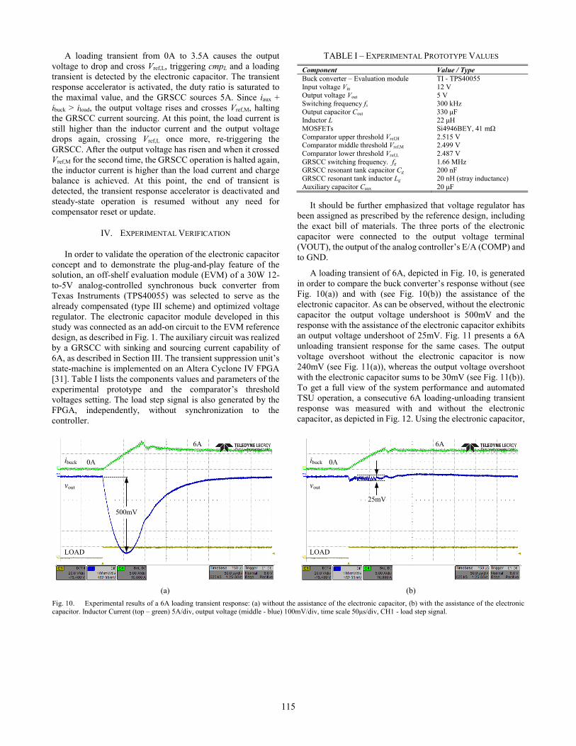
A loading transient of 6A, depicted in Fig. 10, is generated
in order to compare the buck converter’s response without (see
Fig. 10(a)) and with (see Fig. 10(b)) the assistance of the
electronic capacitor. As can be observed, without the electronic
capacitor the output voltage undershoot is 500mV and the
response with the assistance of the electronic capacitor exhibits
an output voltage undershoot of 25mV. Fig. 11 presents a 6A
unloading transient response for the same cases. The output
voltage overshoot without the electronic capacitor is now
240mV (see Fig. 11(a)), whereas the output voltage overshoot
with the electronic capacitor sums to be 30mV (see Fig. 11(b)).
To get a full view of the system performance and automated
TSU operation, a consecutive 6A loading-unloading transient
response was measured with and without the electronic
capacitor, as depicted in Fig. 12. Using the electronic capacitor,
vout
ibuck
LOAD
25mV
0A
6A
(b)
vout
ibuck
LOAD
500mV
0A
6A
(a)
Fig. 10. Experimental results of a 6A loading transient response: (a) without the assistance of the electronic capacitor, (b) with the assistance of the electronic capacitor. Inductor Current (top – green) 5A/div, output voltage (middle - blue) 100mV/div, time scale 50μs/div, CH1 - load step signal.
TABLE I – EXPERIMENTAL PROTOTYPE VALUES
Component Value / Type
Buck converter – Evaluation module TI - TPS40055
Input voltage Vin 12 V Output voltage Vout 5 V
Switching frequency fs 300 kHz
Output capacitor Cout 330 μF Inductor L 22 μH
MOSFETs Si4946BEY, 41 mΩ
Comparator upper threshold Vref,H 2.515 V Comparator middle threshold Vref,M 2.499 V
Comparator lower threshold Vref,L 2.487 V
GRSCC switching frequency. fg 1.66 MHz GRSCC resonant tank capacitor Cg 200 nF
GRSCC resonant tank inductor Lg 20 nH (stray inductance)
Auxiliary capacitor Caux 20 μF
115

the total transient time is only limited by the slew-rate of the
inductor current, which are 80µs for loading and 30µs for
unloading, whereas for the system without the electronic
capacitor the total transient times are 500µs and 275µs,
respectively.
Fig. 13 zooms in to the electronic capacitor operation which
is based on the reference voltages Vref,H and Vref,M for an
unloading event. As can be observed, the electronic capacitor
maintains the output voltage between the two thresholds, sinks
current when the output voltage crosses Vref,H and halts the
operation when the output voltage reaches Vref,M. This leads to
the conclusion that the output voltage deviation for a system
with the electronic capacitor is now determined by the
comparator’s thresholds, and that minimizing the difference
between these thresholds is a function of: (1), the steady-state
voltage ripple and the noise in the system. As a result, the output
capacitance can be significantly reduced and sized to the
steady-state specifications of the output voltage ripple, as
opposed to sizing by the requirements of load transients.
V. CONCLUSION
A plug-and-play electronic capacitor for improved loading
and unloading transient response of voltage regulator modules
has been presented. The improvement has been achieved by the
addition of a load-side transient suppression unit, implemented
by a recently presented GRSCC topology. The electronic
capacitor circuit has three ports and can be connected as an add-
on unit to any closed-loop power supply with external
compensation network, or access to the PWM generator. The
output capacitance can be significantly reduced at the cost of
vout
ibuck
LOAD
30mV
0A
6A
(b)
vout
ibuck
LOAD
240mV
0A
6A
(a)
Fig. 11. Experimental results of a 6A unloading transient response: (a) without the assistance of the electronic capacitor, (b) with the assistance of the electronic
capacitor. Inductor Current (top – green) 5A/div, output voltage (middle - blue) 100mV/div, time scale 50μs/div, CH1 - load step signal.
vout
ibuck
LOAD
0A
6A
0A
With EC
With EC
Without EC
Without EC
Fig. 12. Experimental results of consecutive 6A loading-unloading
transients and the response of the system with and without the electronic capacitor. Inductor Current (top) 5A/div, output voltage (middle) 200mV/div,
time scale 100μs/div, CH1 - load step signal.
vout
ibuck
LOAD
Vref,H
Vref,M
0A
6A
Fig. 13. Experimental results of a 6A unloading transient response showing
the effective reference voltages based operation of the electronic capacitor. Inductor Current (top) 5A/div, output voltage (middle) 50mV/div, time scale
10μs/div, CH1 - load step signal.
116
small additional semiconductors and few capacitors, with no
ferromagnetic elements, and therefore has the potential to be
space conserving and cost-effective when integrated on-chip.
The experimental results demonstrated the performance and
benefits of the new transient suppression approach for both
loading and unloading transients when applied on an off-shelf
commercial buck converter specified by its reference design.
Using the electronic capacitor, the output voltage deviation is
reduced by up to 20 times compared to the original design along
with settling time that is up to 9 times shorter, providing a
strong evidence for a significant volume reduction capability.
ACKNOWLEDGEMENTS
This research is supported by Vishay Ltd., Siliconix division.
REFERENCES
[1] E. A. Burton, G. Schrom, F. Paillet, J. Douglas, W. J. Lambert, K.
Radhakrishnan, and M. J. Hill, “FIVR — Fully integrated voltage regulators on 4th generation Intel® Core™ SoCs,” in Proc. IEEE Appl.
Power Electron. Conf. Expo. 2014, pp. 432-439, Mar. 2014.
[2] S. Abedinpour, B. Bakkaloglu, and S. Kiaei, “A multistage interleaved synchronous buck converter with integrated output filter in 0.18μm SiGe
process,” IEEE Trans. Power Electron., vol. 22, no. 6, pp. 2164–2175,
Nov. 2007. [3] G. Schrom, “A 100 MHz eight-phase buck converter delivering 12 A in
25 mm^2 using air-core inductors,” in Proc. IEEE Appl. Power Electron.
Conf. Expo. 2007, pp. 727-730, Mar. 2007. [4] S. Ahsanuzzaman, A. Parayandeh, A. Prodic, and D. Maksimovic,
“Loadinteractive steered-inductor dc–dc converter with minimized
output filter capacitance,” in Proc. IEEE Appl. Power Electron. Conf. Expo. 2010, pp. 980–985, Feb. 2010.
[5] M. del Viejo, P. Alou, J. A. Oliver, O. Garcia, and J. A. Cobos, “Fast
control technique based on peak current mode control of the output capacitor current,” in Proc. IEEE Energy Convers. Congr. Expo., pp.
3396–3402, Sep. 2010.
[6] M. del Viejo, P. Alou, J. A. Oliver, O. Garcia, and J. A. Cobos, “V2IC control: A novel control technique with very fast response under load
and voltage steps,” in Proc. IEEE Appl. Power Electron. Conf. Expo.
2011, pp. 231–237, Mar. 2011. [7] J. Chen, A. Prodić, R. Erickson, and D. Maksimović, “Predictive digital
current programmed control,” IEEE Trans. Power Electron., vol. 18, no.
1, pp. 411–419, Jan. 2003. [8] S. Chattopadhyay and S. Das, “A digital current-mode control technique
for dc-dc converters,” IEEE Trans. Power Electron., vol. 21, no. 6, pp.
1718–1726, Nov. 2006. [9] Y. Qiu, X. Chen, and H. Liu, “Digital average current-mode control
using current estimation and capacitor charge balance principle for dc-
dc converters operating in DCM,” IEEE Trans. Power Electron., vol. 25, no. 6, pp. 1537–1545, Jun. 2010.
[10] P. Midya, P. T. Krein, and M. F. Greuel, “Sensorless current mode
control-an observer-based technique for DC-DC converters,” IEEE Trans. Power Electron., vol. 16, pp. 522 – 526. 2001.
[11] A. Babazadeh and D. Maksimović, “Hybrid digital adaptive control for
fast transient response in synchronous buck DC–DC converters,” IEEE Trans. Power Electron., vol. 24, no. 11, pp. 2625 – 2638, Nov. 2009.
[12] L. Corradini, A. Costabeber, P. Mattavelli, and S. Saggini, “Parameter-
independent time-optimal digital control for point-of-load converters,” IEEE Trans. Power Electron., vol. 24, no. 10, pp. 2235–2248, Oct. 2009.
[13] A. Babazadeh, L. Corradini, and D. Maksimović, “Near time-optimal transient response in DC-DC buck converters taking into account the
inductor current limit,” in Proc. IEEE Energy Convers. Conf. Expo., Sep.
2009, pp. 3328–3335. [14] V. Yousefzedah, A. Babazadeh, B. Ramachandran, E. Alarcon, L. Pao,
and D. Maksimović, “Proximate time-optimal control for synchronous
buck DC–DC converters,” IEEE Trans. Power Electron., vol. 23, no. 4, pp. 2018–2026, Jul. 2008
[15] L. Corradini, A. Babazadeh, A. Bjeletić, and D. Maksimović, “Current-
limited time-optimal response in digitally controlled dc–dc converters,” IEEE Trans. Power Electron., vol. 25, no. 11, pp. 2869–2880, Nov. 2010
[16] G. E. Pitel and P. T. Krein, “Minimum-time transient recovery for DC–
DC converters using raster control surfaces,” IEEE Trans. Power Electron., vol. 24, no. 12, pp. 2692 - 2703, Dec. 2009.
[17] E. Meyer, Z. Zhang, and Y. F. Liu, “An optimal control method for buck
converters using a practical capacitor charge balance technique”, IEEE Trans. Power Electron., vol. 23, no. 4, pp. 1802-1812, Jul. 2008.
[18] A. Radić, Z. Lukić, A. Prodić, and R. de Nie, “Minimum deviation
digital controller IC for DC-DC switch-mode power supplies,” IEEE Trans. Power Electron, vol. 28, no. 9, pp. 4281-4298, Sep. 2013.
[19] A. Stupar, Z. Lukić, and A. Prodić, “Digitally-controlled steered-
inductor buck converter for improving heavy-to-light load transient response,” in Proc. IEEE Power Electron. Spec. Conf. 2008, pp. 3950–
3954, Jun. 2008.
[20] W. Jing, A. Prodić, and W. T. Ng , “Mixed-signal-controlled flyback-transformer-based buck converter with improved dynamic performance
and transient energy recycling,“ IEEE Trans. Power Electron , vol. 28,
no. 2, pp. 970-984, Feb. 2013. [21] P.S. Shenoy, P.T. Krein, and S. Kapat, "Beyond time-optimality:
Energy-based control of augmented buck converters for near ideal load
transient response," in Proc. IEEE Appl. Power Electron. Conf. Expo. 2011, pp. 916-922, Mar. 2011
[22] Y. Wen and O. Trescases, “DC-DC converter with digital adaptive slope
control in auxiliary phase for optimal transient response and improved efficiency,” IEEE Trans. Power Electron., vol. 27, no. 3, pp. 1314–1326,
Mar. 2012.
[23] E. Meyer, Z. Zhang, and Y. F. Liu, “Controlled auxiliary circuit to improve unloading transient response of buck converters,” IEEE Trans.
Power Electron., vol. 25, no. 4, pp. 806–819, Apr. 2010.
[24] V. Svikovic, J. A. Oliver, P. Alou, O. García, and J. A. Cobos,
“Synchronous buck converter with output impedance correction circuit,”
IEEE Trans. Power Electron., vol. 28, no. 7, pp. 3415–3427, Jul. 2013. [25] V. Svikovic, J. J. Cortes, P. Alou, J. A. Oliver, O. Garcia, and J. A.
Cobos, “Multiphase current-controlled buck converter with energy
recycling output impedance correction circuit (OICC),” IEEE Trans. Power Electron., vol. 30, no. 9, pp. 5207-5222, Sep. 2015
[26] Z. Shan, S. C. Tan, and C. K. Tse, “Transient mitigation of dc-dc
converters for high output current slew rate applications,” IEEE Trans. Power Electron., vol. 28, no. 5, pp. 2377–2388, May 2013.
[27] O. Kirshenboim, A. Cervera, and M. M. Peretz, “Improving loading and
unloading transient response of a voltage regulator module using a load-side auxiliary gyrator circuit”, in Proc. IEEE Appl. Power Electron.
Conf. Expo. 2015, pp. 913-920, Mar. 2015.
[28] A. Cervera, M. Evzelman, M.M. Peretz, and S. Ben-Yaakov, “A high efficiency resonant switched capacitor converter with continuous
conversion ratio,” IEEE Trans. Power Electron., vol. 30, no. 3, pp. 1373-
1382, Mar. 2015.
[29] B. C. Kuo, Automatic Control Systems, Englewood Cliffs, NJ, Prentice-
Hall, 1982.
[30] A. Cervera and M. M. Peretz, “Resonant switched-capacitor voltage regulator with ideal transient response,” IEEE Trans. Power Electron.,
vol. 30, no. 9, pp. 4943-4951, Sep. 2015.
[31] DE2 Development and Education Board user manual, Altera Corporation, 2006.
117