plasmonics: application-oriented fabrication part 2 ... · plasmonics: application-oriented...
TRANSCRIPT

August 25, 2013 ICQNM 2013 Barcelona, Spain 1
Plasmonics: Application-oriented fabrication
Part 2. Applications and technological challenges
Victor Ovchinnikov
Department of Aalto NanofabAalto UniversityEspoo, Finland

Outline
• Main plasmonic applications and requirements to technology
• Plasmonic device in general
• Ideal nanofabrication process for plasmonics
August 25, 2013 ICQNM 2013 Barcelona, Spain 2
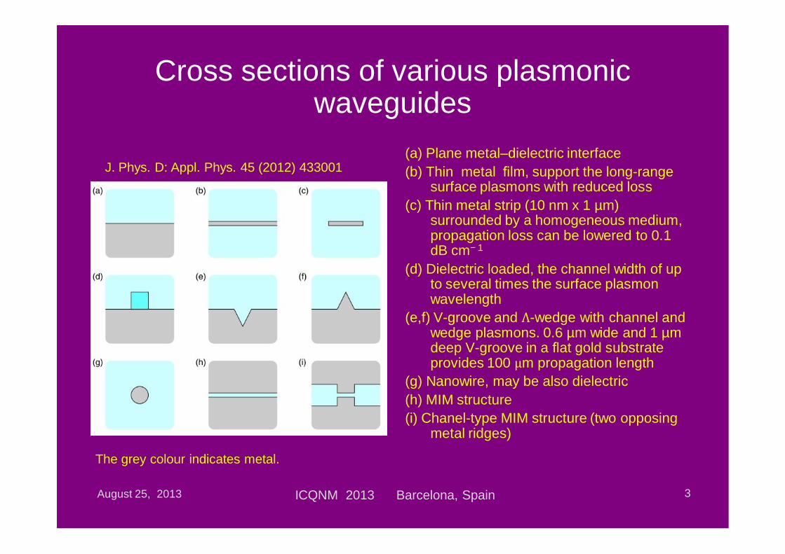
Cross sections of various plasmonicwaveguides
(a) Plane metal–dielectric interface(b) Thin metal lm, support the long-range
surface plasmons with reduced loss(c) Thin metal strip (10 nm x 1 µm)
surrounded by a homogeneous medium, propagation loss can be lowered to 0.1 dB cm 1
(d) Dielectric loaded, the channel width of up to several times the surface plasmonwavelength
(e,f) V-groove and -wedge with channel and wedge plasmons. 0.6 µm wide and 1 µm deep V-groove in a at gold substrate provides 100 m propagation length
(g) Nanowire, may be also dielectric(h) MIM structure(i) Chanel-type MIM structure (two opposing
metal ridges)
August 25, 2013 ICQNM 2013 Barcelona, Spain 3
The grey colour indicates metal.
J. Phys. D: Appl. Phys. 45 (2012) 433001
Waveguide fabrication
• Requirements:– Regular structures– Non-rectangular profile (optional)– Metallization of internal surfaces– Small chip on a large wafer– High volume production
• Methods:– Nanoimprint– Damascene
August 25, 2013 ICQNM 2013 Barcelona, Spain 4

SPP sensor
August 25, 2013 ICQNM 2013 Barcelona, Spain 5
Ann. Phys. (Berlin) 524, No. 11, 637–662 (2012) / DOI 10.1002/andp.201200203
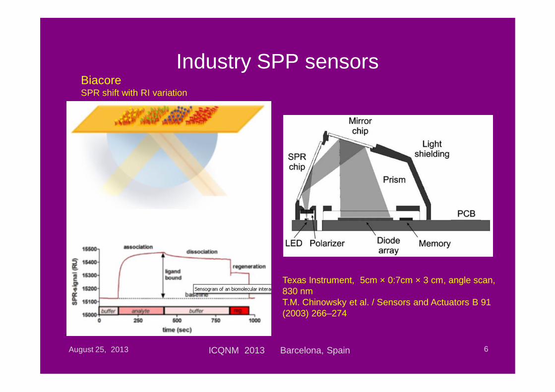
Industry SPP sensors
August 25, 2013 ICQNM 2013 Barcelona, Spain 6
BiacoreSPR shift with RI variation
Texas Instrument, 5cm × 0:7cm × 3 cm, angle scan, 830 nmT.M. Chinowsky et al. / Sensors and Actuators B 91 (2003) 266–274

Biosensor with plasmonics-enabled detection
August 25, 2013 ICQNM 2013 Barcelona, Spain 7
1 m
G. Brolo, NATURE PHOTONICS | VOL 6 | NOVEMBER 2012 | p.709
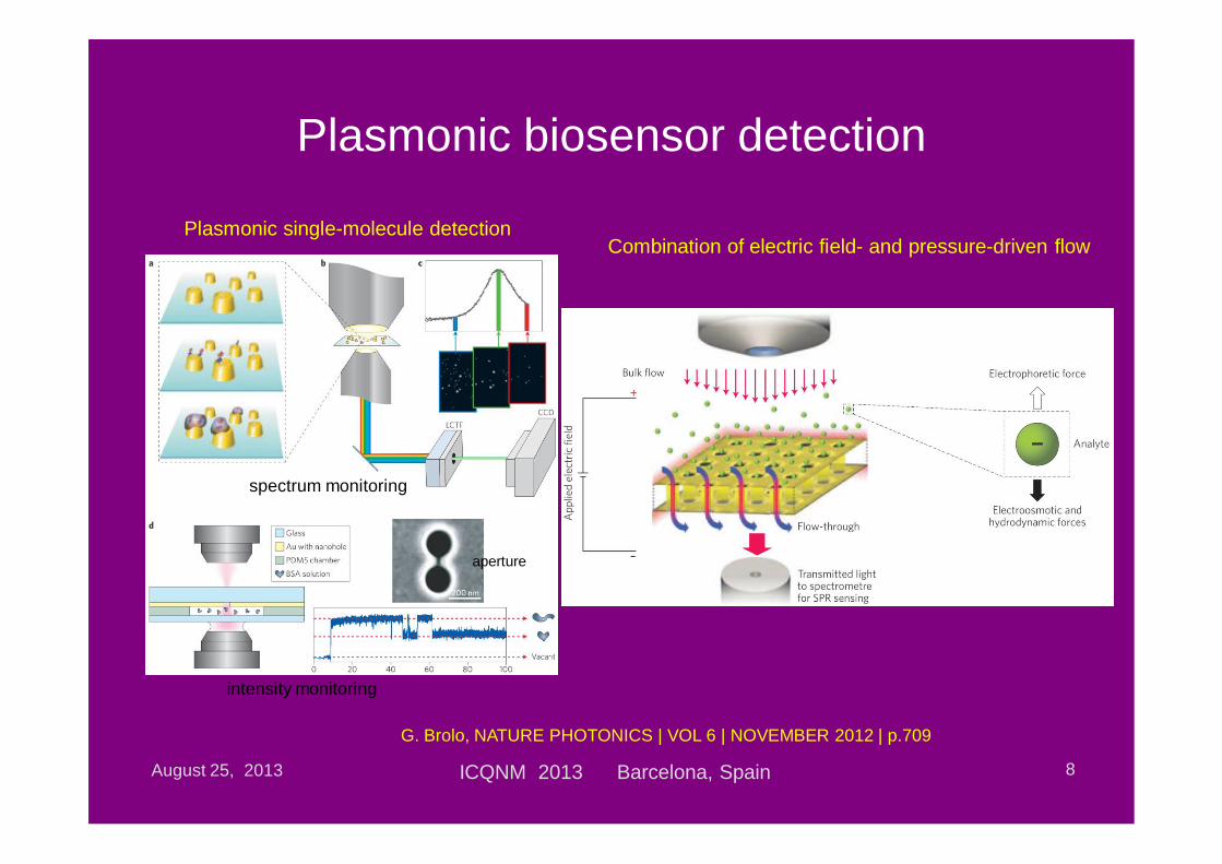
Plasmonic biosensor detection
August 25, 2013 ICQNM 2013 Barcelona, Spain 8
G. Brolo, NATURE PHOTONICS | VOL 6 | NOVEMBER 2012 | p.709
Combination of electric field- and pressure-driven flowPlasmonic single-molecule detection
spectrum monitoring
intensity monitoring
aperture
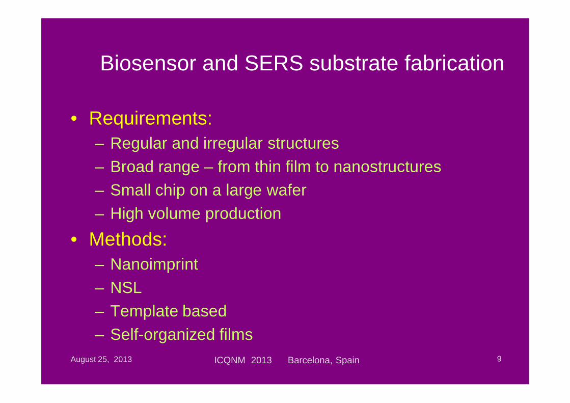
Biosensor and SERS substrate fabrication
• Requirements:– Regular and irregular structures– Broad range – from thin film to nanostructures– Small chip on a large wafer– High volume production
• Methods:– Nanoimprint– NSL– Template based– Self-organized films
August 25, 2013 ICQNM 2013 Barcelona, Spain 9

Commersial SERS substrate (Klarite)
August 25, 2013 ICQNM 2013 Barcelona, Spain 10
www.d3technologies.co.uk - www.renishawdiagnostics.com/en/klarite-sers-substratesZHIDA XU, Master Thesis, University of Illinois at Urbana-Champaign, 2011
785 nm
c-Si
E/E0
Very high enhancements are ‘sacri ced’ in favor of homogeneity and reproducibility

Leaning Si pillars
August 25, 2013 ICQNM 2013 Barcelona, Spain 11
M.S. Schmidt et al., Adv. Mater. 2012, 24, OP11–OP18 no leaning leaning

SERS, distance dependence
August 25, 2013 ICQNM 2013 Barcelona, Spain 12
Stiles P.L. et all, Annual Review of Analytical Chemistry, 1, 2008, p.601-26
Pyridine, Ag over nanosphere, Al2O3, 532 nm

Nonlinear plasmonics
• Nonlinear optical effects arise when electronic motion in a strong electromagnetic field cannot be considered harmonic. For applications, the most important effects occur at second (SHG) and third harmonics.
• Two ways to enhance nonlinear effects:– plasmonic structures provide field enhancement near the metal–dielectric
interface (intrinsic and extrinsic response) – plasmonic excitation parameters (SPP wavevector and the LSP
resonance frequency) are very sensitive to the refractive indices of the metal and the surrounding dielectric, which are nonlinearly changed.
• Centrosymmetry is detrimental to second-order response even in the presence of local-field enhancement
• Nonlinear effects are utilized with reduced power• Scale down nonlinear component in size• The response time is ultrafast (femtosecond timescale)
August 25, 2013 ICQNM 2013 Barcelona, Spain 13

Structured metal surfaces for nonlinear plasmonics
August 25, 2013 ICQNM 2013 Barcelona, Spain 14
A. Zayats, NATURE PHOTONICS| VOL 6 | NOVEMBER 2012 | p.737

Plasmonic systems for enhancingnonlinear optical Kerr effect
August 25, 2013 ICQNM 2013 Barcelona, Spain 15
10 nm diameter silver par-ticles embedded in carbon disulfid 500 × 440 nm 2 nonlinear waveguide-ring resonator
Nonlinear gold nanoantenna with 20 nm gapDirect modulation of the SPP signal
A. Zayats, NATURE PHOTONICS| VOL 6 | NOVEMBER 2012 | p.737

Nonlinear plasmonic fabrication
• Requirements:– Regular asymmetrical structures– Small substrates– Low volume production
• Methods:– EBL– FIB– Nanoimprint– NSL
August 25, 2013 ICQNM 2013 Barcelona, Spain 16

SPR and photovoltaics
• Enhancement of the local field• Enlargement of the scattereing cross-section by
LPR• Confinment using MIM modes• Coupling of the incident light to waveguide
modes
August 25, 2013 ICQNM 2013 Barcelona, Spain 17

Plasmonic solar cells
August 25, 2013 ICQNM 2013 Barcelona, Spain 18
J. Phys. D: Appl. Phys. 45 (2012) 433001

Plasmonic solar cell fabrication
• Requirements:– Regular and random arrays– Large area substrates– Multilayer structure– High volume production– Rough (non-flat) surface above pn-junctions and
metallization• Methods:
– NSL– Shadow (stencil) mask– Self-organizing films
August 25, 2013 ICQNM 2013 Barcelona, Spain 19

Chip area and volume of production
• Chip area, based on functional properties:– SERS – small area, small to large volume– Metamaterials – large area, small to large volume– Waveguides – small area, large volume– Solar cells – large area, large volume– Sensors – small area, large volume– Non linear plasmonics – small area, small volume
August 25, 2013 ICQNM 2013 Barcelona, Spain 20

Plasmonic device in general
• Combination of metal and dielectric parts• Critical dimensions are 20 – 150 nm• Metal thickness is 50 – 200 nm• Metal part separation is 2 – 200 nm• Multilayer design (optional)• Non rectangular shape (spheres, rods, groovs,
rings)• Large area devices• Integrated part of more complicate devices
August 25, 2013 ICQNM 2013 Barcelona, Spain 21

Fabrication problems of plasmonics
• No dry etching methods, but Al in Cl2
• Large area is totally covered by small structires with critical dimensions. Compare to CMOS – channnel area is the small fraction of total area
• Ag and Au are killers of electronic properties of semiconductors. They have large diffusion coefficients in volume and on the surface
• High temperature processing is limited by 500 C
• Smooth metal surface is required (optional)
August 25, 2013 ICQNM 2013 Barcelona, Spain 22

Main steps of plasmonic nanofabrication
• Formation of the functional layer• Patterning• Transfer the pattern into the functional layer• Formation of interlayer dielectric• Planarization
August 25, 2013 ICQNM 2013 Barcelona, Spain 23

Formation of metal layer
• Physical vapour deposition (PVD)– e-beam evaporation– sputtering– pulsed laser deposition– ion beam sputtering
• Electroplating, limited number of metals, roughness
• Atomic layer depostion (ALD): Ru, Pt, Au, Ag. Good conformality, bad metal quality
August 25, 2013 ICQNM 2013 Barcelona, Spain 24

Patterning
• Optical lithography– Contact mask, limited by 1µm resolution– Stepper, 22 nm with phase shift mask and double
patterning lithography• Scanning beam lithography
– Electron beam lithography (EBL)– Focused ion beam (FIB)
• Shadow mask (stencil)• Self-organized masks
August 25, 2013 ICQNM 2013 Barcelona, Spain 25

Pattern transfer
• Etching– Wet– Dry
• Lift-off (reverse pattern)• Selective deposition (growth)• Chemical mechanical polishing (CMP)
August 25, 2013 ICQNM 2013 Barcelona, Spain 26

Scanning beam lithography
• Scanning beam lithographies are capable of precise control over the size, shape, and spacing of metallic nano-structures
• Low throuhput
• EBL can be used to attain sub-20 nm resolution using specialized resists such as hydrogen silsesquioxane (HSQ) or NaCl crystals
• FIB is a related technique that uses a focused beam of ions (typically Ga+) to perform both additive and subtractive patterning by physical or chemically assisted processes. These include:
– FIB milling,– ion-assisted etching,– FIB-induced deposition
• FIB is capable of forming patterns with 10 nm resolution using either PMMA or inorganic resists.
August 25, 2013 ICQNM 2013 Barcelona, Spain 27

Optical lithography
August 25, 2013 ICQNM 2013 Barcelona, Spain 28
PR pattern
SiO2 pattern
SiO2
PR
Lift-off Direct etching

Lift-off vs. direct etching II
• Lift-off:– resist layer should be at least twice as thick as the lift-off thickness (metal),
i.e. limited aspect ratio of metal structures– vertical mask sidewalls or overhanging structures– easy to remove mask, high chemical activity– functional layer is deposited on residues that left after mask fabrication– patterned layer particles are left in the solvent and redeposit on the sample– rough edge of the pattern, due to film destroying
• Direct etching:– mask thickness is not connected with etched layer thickness. It depends on
etching chemistry– shape of mask sidewalls is not critical– functional layer is deposited on clean or prepared surface
• Result:– direct etching provides smaller critical dimensions, higher reproducibility and
better areal uniformity
August 25, 2013 ICQNM 2013 Barcelona, Spain 29
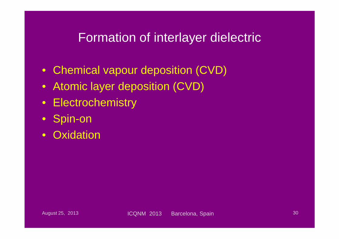
Formation of interlayer dielectric
• Chemical vapour deposition (CVD)• Atomic layer deposition (CVD)• Electrochemistry• Spin-on• Oxidation
August 25, 2013 ICQNM 2013 Barcelona, Spain 30

Planarization
• Etchback
• Chemical mechanical polishing
August 25, 2013 ICQNM 2013 Barcelona, Spain 31

Damascene process – solution for plasmonics
August 25, 2013 ICQNM 2013 Barcelona, Spain 32
Oxide deposition
Wire lithography, RIE of oxide
Metal stack depostion
Chemical mechanical polishing (CMP)

Damascene process features
• Bottom seed layer:– PR mask with metal pattern– selective electroplating– PR mask removing (Ag corrosion)– seed layer removing (problem, because structure thickness and seed layer
are similar; for dry removing pattern deteriorates, for wet – stop time and pattern deteriorate; ALD thin seed layer – change plasmonic properties)
• Top seed layer:– SiO2 mask– blank electroplating– CMP of metal– SiO2 remove – works!
• Space between metal parts about twice of CD! Impossible produce small dimers
• ALD – bad metal quality
August 25, 2013 ICQNM 2013 Barcelona, Spain 33
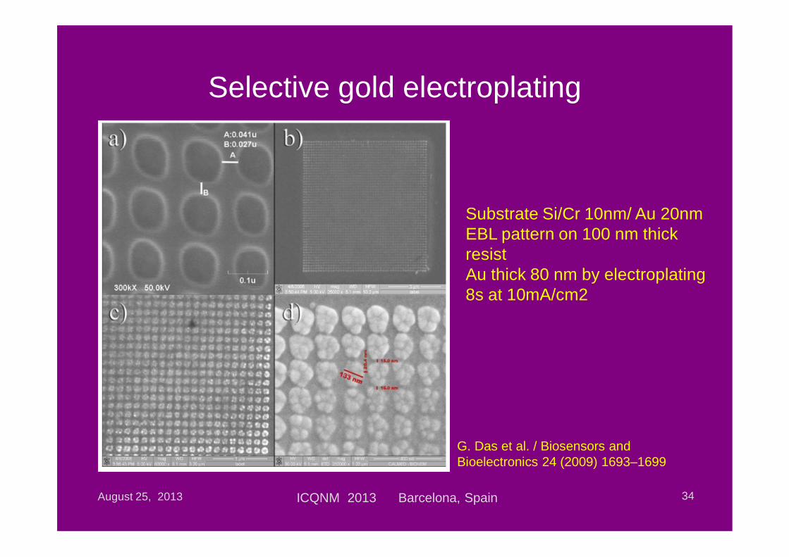
Selective gold electroplating
August 25, 2013 ICQNM 2013 Barcelona, Spain 34
G. Das et al. / Biosensors and Bioelectronics 24 (2009) 1693–1699
Substrate Si/Cr 10nm/ Au 20nmEBL pattern on 100 nm thick resistAu thick 80 nm by electroplating 8s at 10mA/cm2

Effect of adhesion layer
August 25, 2013 ICQNM 2013 Barcelona, Spain 35
50 nm thick Au SRRs on a 1 mm thick fused silica substrate. Side length 200 nm, height=50 nm, period 500 nm
Appl. Phys. Lett.97, 263103 (2010)
Spin on electron resist (150 nm) Deposition of 15 nm Al layer to prevent charge accumulation.EBL, 1.2×1.2 mm2 area , 100 kV, 200 µC/cm2 , 2 nA current, 6 nm spotsizeAl iremove and developingO2 plasma descumDeposition of a 2–5 nm adhesion layer, Ti or ITO, and 50 nm Au.The final lift-off is.

Random mask with adhesion layer
August 25, 2013 ICQNM 2013 Barcelona, Spain 36
Mask
Substrate
Dry etching
Mask removing
Maskresidues
Template
Evaporation Adhesionlayer
Functionallayer
Functionallayer
Evaporation Inclined evaporation
Substrate rotation
V. Ovchinnikov ,Proceedings of ICQNM 2011, ThinkMind Digital Library, pp. 6-11

Self-organized metal with adhesion layer
August 25, 2013 ICQNM 2013 Barcelona, Spain 37
Normal evaporation
Ti=1 nmAu=8nm,tilted 30º
Evaporation angle 70º
Au=8nm,tilted 30º
Ti=1 nmAg=8nm,tilted 30º
Ag=8nm,tilted 30º

Intermediate conclusion II
• Reproducible fabrication of metal nanostructures is still main problem of plasmonics
• Small area samples for research purposes are easily fabricated by beam lithography and lift-off
• Large area samples are mainly limited in design:– random arrays for template lithography– limited ratio of size to space for interference
lithography
August 25, 2013 ICQNM 2013 Barcelona, Spain 38