plasmonic analogue of electromagnetically induced ... paid to the fact that eit-like effects can...
TRANSCRIPT

ARTICLESPUBLISHED ONLINE: 5 JULY 2009 | DOI: 10.1038/NMAT2495
Plasmonic analogue of electromagneticallyinduced transparency at the Drude damping limitNa Liu1, Lutz Langguth1, ThomasWeiss1, Jürgen Kästel2, Michael Fleischhauer2, Tilman Pfau3
and Harald Giessen1*In atomic physics, the coherent coupling of a broad and a narrow resonance leads to quantum interference and providesthe general recipe for electromagnetically induced transparency (EIT). A sharp resonance of nearly perfect transmission canarise within a broad absorption profile. These features show remarkable potential for slow light, novel sensors and low-lossmetamaterials. In nanophotonics, plasmonic structures enable large field strengths within small mode volumes. Therefore,combining EIT with nanoplasmonics would pave the way towards ultracompact sensors with extremely high sensitivity. Here,we experimentally demonstrate a nanoplasmonic analogue of EIT using a stacked optical metamaterial. A dipole antenna witha large radiatively broadened linewidth is coupled to an underlying quadrupole antenna, of which the narrow linewidth is solelylimited by the fundamental non-radiative Drude damping. In accordance with EIT theory, we achieve a very narrow transparencywindow with high modulation depth owing to nearly complete suppression of radiative losses.
Electromagnetically induced transparency (EIT) is a quantuminterference effect that reduces light absorption over a narrowspectral region in a coherently driven atomic system1–3.
Associated with the enhanced transmission is a drastic modificationof the dispersive properties of themedium, which enables light to beslowed down substantially4–7. Recently, a lot of attention has beenpaid to the fact that EIT-like effects can occur in classical oscillatorsystems. Examples include coupled microresonators8, electriccircuits9, a waveguide side-coupled to resonators10,11 and metallicstructures12. In particular, the theoretical prediction of plasmon-induced transparency has been brought forward13. However, sofar experimental attempts to realize these theoretical proposalsin optical plasmonic systems have not been successful owing todifficulties associated with nanofabrication. Very recently, Fanoresonances within an absorption band have been experimentallyobserved in non-optimized single plasmonic structures at opticalfrequencies14. The broad linewidth and small modulation depth ofthose resonances, however, severely hamper applications such asslowing down light, which requires an abrupt change in dispersionover a narrow spectral range, as well as sensing, where a sharp andpronounced spectral response is highly desired15.
Here, we provide the first experimental demonstration ofEIT-like effects in optical metamaterials. The structure of thisnanoplasmonic analogue of EIT consists of two functional layers,where each unit cell comprises a gold bar stacked above twosymmetric gold wires (Fig. 1a). The elements in the two layersare oriented perpendicular to each other. More specifically, thetop gold bar serves as a broad-linewidth dipole antenna. It isstrongly coupled to light, therefore suffering significant losses dueto radiative damping. The bottom gold wire pair can act as anon-radiative quadrupole antenna and its resonance frequencyis adjusted within the absorbance profile of the dipole antenna.The damping of the quadrupole antenna stems almost exclusivelyfrom intrinsic metal losses (Drude damping), and is much smallerthan the radiative damping of the dipole antenna. Owing to
14. Physikalisches Institut, Universität Stuttgart, D-70569 Stuttgart, Germany, 2Fachbereich Physik and Research Center OPTIMAS, Technische UniversitätKaiserslautern, D-67663 Kaiserslautern, Germany, 35. Physikalisches Institut, Universität Stuttgart, D-70569 Stuttgart, Germany.*e-mail: [email protected].
close proximity, the two antennas can be strongly coupled. As aconsequence, destructive interference between the two excitationpathways leads to the EIT-like phenomena. These two pathwaysare the direct excitation of the dipole antenna by the externallight field and the excitation by the coupling with the quadrupoleantenna. On the contrary, if the underlying quadrupole antennais replaced by a dipole antenna, which has similar damping to theupper one, the destructive interference disappears and no enhancedtransmission effect can be observed. This is the distinctive signatureof normal-mode splitting in contrast to EIT behaviour. In addition,we experimentally demonstrate that the EIT-like spectra can bemodified by varying the coupling strength between the dipoleand quadrupole antennas by means of accurate structural tuning.The agreement between experiment and a simple EIT model3,9 isnearly perfect. Moreover, we demonstrate that our experimentalabsorbance linewidth is limited only by Drude damping. Theresulting narrow, yet fully modulated EIT-like features, renderour nanoplasmonic system ideal for slow light and novel sensorswith high sensitivity16.
Figure 1a schematically shows the metamaterial structure. Theupper gold bar (in red) is stacked above the underlying gold wirepair (in green) with a vertical distance h = 70 nm. The lateraldisplacement of the bar with respect to the symmetry axis of thewirepair is defined as s. Electron micrographs of the samples fabricatedby nanofabrication stacking techniques17 were obtained by field-emission scanning electronmicroscopy. Figure 1b shows an obliqueincidence overview of a typical sample with a lateral displacements = 10 nm. An enlarged oblique view is given in the inset ofFig. 1b, demonstrating excellent alignment accuracy between thetwo functional layers. The optical properties of the samples atnormal incidence weremeasured with a Fourier-transform infraredspectrometer with electric field polarization along the dipoleantenna. In the following, we are going to show systematic tuningof the EIT-like spectra in these stacked samples by introducingstructural asymmetry. The experimental transmittance (green
NATUREMATERIALS | ADVANCE ONLINE PUBLICATION | www.nature.com/naturematerials 1© 2009 Macmillan Publishers Limited. All rights reserved.

ARTICLES NATURE MATERIALS DOI: 10.1038/NMAT2495
E (x)
H (y)k (z)
w
w
st
g
l1
l2
h
t
2 µm
a
b
Figure 1 | Structural geometry and field-emission electron microscopyimages. a, Schematic diagram of the stacked plasmonic EIT structure withdefinitions of the geometrical parameters: l1= 355 nm, l2= 315 nm,w=80 nm, g=220 nm, t=40 nm and h=70 nm. The periods in both the xand y directions are 700 nm. Red colour represents the gold bar in the toplayer and green colour represents the gold wire pair in the bottom layer.b, Oblique view of the sample with lateral displacement s= 10 nm. Inset:Enlarged view. All of the structures were fabricated on a glass substrate.The gold wires were embedded in a photopolymer (PC403), which servesas a dielectric spacer.
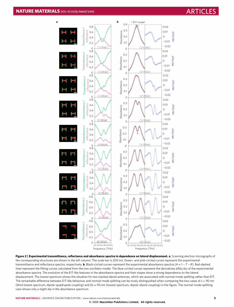
circles), reflectance (pink circles) and absorbance spectra (blackcircles) in dependence on the lateral displacement s are presented inFig. 2. The absorbance spectra were calculated using A= 1−T−R.In the absence of structural asymmetry, that is, for s=0, there is onlya single resonance (ω0 = 170 THz) observable in the absorbancespectrum (see Fig. 2b). The origin of this resonance is attributedto the excitation of dipole-like plasmons inside the upper gold bar.This gold bar works as a dipole antenna and radiates strongly to freespace, giving rise to a broad resonance in the spectrum. The lowerwires do not contribute, as the elements in the two layers are notcoupled to each other in the absence of symmetry breaking.
The coupling between the two layers starts once the structuralasymmetry is introduced. As visible in the case of s = 10 nm, atransmittance peak in Fig. 2a (an absorbance dip in Fig. 2b) ataround 173 THz emerges near the centre of the broad resonance.A detuning parameter δ is introduced to define the frequencydifference between the quadrupole and dipole resonances. In ourcase, δ is approximately 3 THz, resulting from slightly too short
bottom wires owing to the fabrication process. By further enlargingthe lateral displacement s, the coupling strength between the dipoleand quadrupole antennas is successively increased. As a result, thetransparency window at 173 THz grows in strength and becomesmore and more prominent as shown in Fig. 2a. We interpret theabove phenomena in terms of plasmonic EIT. Particularly, thenarrow linewidths and high modulation depths of these EIT-likefeatures indicate the drastically low loss in the quadrupole antenna.The physics of the plasmonic EIT can be better understood if we ex-amine the analogy between our system and atomic EIT systems3,13.Figure 3a shows a prototype three-level system for EIT, in which |0〉is the ground state and |1〉 and |2〉 are the two upper states. |0〉–|1〉defines a dipole-allowed transition, which is in analogy to the modeexcited in the dipole antenna in our system. It is related to a photonfrequency ω0 and a dissipation rate γ1. This rate includes twocontributions, namely, radiative damping due to the transforma-tion of particle plasmons into photons and non-radiative dampingdue to the intrinsic metal loss. |0〉–|2〉 defines a dipole-forbiddentransition, which is in analogy to the mode that can be excited inthe quadrupole antenna when structural asymmetry is present. It ischaracterized by a dissipation rate γ2, which is mainly limited by theintrinsic metal loss. δ denotes the detuning from the transition linecentre with the condition δ� γ1. The two damping factors satisfyγ2� γ1� ω0. The transition rate, κ , between states |1〉 and |2〉is correlated with the coupling between the dipole and quadrupoleantennas. Consequently, the two possible pathways, namely, |0〉–|1〉and |0〉–|1〉–|2〉–|1〉 interfere destructively, therefore dramaticallyreducing losses and enhancing transmittance.
To further explore the EIT-like spectral characteristics, opticalspectra and the electric field distribution are calculated on thebasis of a scattering matrix algorithm18 and on commercial finite-integration time-domain software. For bulk gold, the permittivityin the infrared spectral regime is described by the Drude model19,20with the plasmon frequency ωpl = 2π × 2.175 × 1015 s−1 andthe damping constant ωc = 2π × 6.5 × 1012 s−1. Owing to thesurface scattering and grain boundary effects in the thin film,in the calculations we use a damping constant that is threetimes21,22 as large as that in bulk gold, that is, about 20 THz. Theoverall agreement between experimental and calculated spectrais very good (see Supplementary Information). The electric fielddistribution at the absorbance dip as indicated by the red triangle inthe case of s= 50 nm (see Fig. 2b) is shown in Fig. 3b. At resonance,the two underlying wires are characterized by antisymmetric chargeoscillations, which correspond to the excitation of the quadrupolemode. The destructive interference leads to a nearly zero electricfield in the top bar. In other words, owing to nearly completesuppression of radiative damping, the linewidth of these EIT-likefeatures is solely limited by non-radiative damping, that is, intrinsicDrude loss of the metal. This makes our plasmonic EIT structuresparticularly promising for biomedical and chemical sensing.
As a control experiment, we also fabricated a stacked samplewithonly a single wire, that is, another dipole antenna, in the bottomlayer.We define the lateral displacement of the topwire with respectto the symmetry axis of the bottom wire as Ds. Similarly, in theabsence of structural asymmetry, that is,Ds=0, the top and bottomwires are uncoupled, giving rise to a single absorbance peak in thespectrum (not shown). When structural asymmetry is introduced,that is, Ds= 90 nm, the two dipole antennas can be coupled. Suchdipole–dipole coupling between the two wires results in a spectralsplitting owing to the hybridization of the resonances of the twoindividual wires23. It is worth mentioning that 90 nm was selectedbecause lateral displacements below this value do not lead toobservable spectral splitting in experiments. The difference betweenthe EIT-like spectrum and the spectrum arising from hybridizationof plasmonic modes is remarkable. This becomes evident whencomparing the two corresponding spectra associated with the same
2 NATUREMATERIALS | ADVANCE ONLINE PUBLICATION | www.nature.com/naturematerials
© 2009 Macmillan Publishers Limited. All rights reserved.
NATURE MATERIALS DOI: 10.1038/NMAT2495 ARTICLES
Tran
smitt
ance
/
refle
ctan
ce
0.8
0.6
0.4
0.2
0
Tran
smitt
ance
/
refle
ctan
ce
0.8
0.6
0.4
0.2
0
Tran
smitt
ance
/
refle
ctan
ce
0.8
0.6
0.4
0.2
0
Tran
smitt
ance
/
refle
ctan
ce
0.8
0.6
0.4
0.2
0
Tran
smitt
ance
/
refle
ctan
ce
0.8
0.6
0.4
0.2
0
Tran
smitt
ance
/
refle
ctan
ce
0.2
0
0
0.8
0.6
0.4
Tran
smitt
ance
/
refle
ctan
ce
0.2
0.8
0.6
0.4
0
Tran
smitt
ance
/
refle
ctan
ce
0.2
0.8
0.6
0.4
0
Tran
smitt
ance
/
refle
ctan
ce
0.2
0.8
0.6
0.4
s = 0 nm s = 0 nm
s = 10 nm s = 10 nm
s = 20 nm s = 20 nm
s = 30 nm s = 30 nm
s = 50 nm s = 50 nm
s = 70 nm s = 70 nm
s = 90 nm s = 90 nm
s = 110 nm s = 110 nm
Ds = 90 nm Ds = 90 nm
a b
0.3
0.2
0.1Abs
orba
nce
Abs
orba
nce
0.40
0
0.3
0.2
0.1
0
Abs
orba
nce
0.3
0.2
0.1
0
Abs
orba
nce
0.3
0.2
0.1
0A
bsor
banc
e
0.3
0.2
0.1
0
Abs
orba
nce
0.3
0.2
0.1
0
Abs
orba
nce
0.3
0.2
0.1
0
Abs
orba
nce
0.3
0.2
0.1
0
Abs
orba
nce
0.3
0.2
0.1
0140 160 180 200
Frequency (THz)120 220 140 160 180 200 120 140 160 180 200
Frequency (THz)120 220
dAbs/d
0.02
0.01
0
¬0.01
¬0.02
ωdA
bs/d
0.02
0.01
0
¬0.01
¬0.02
ωdA
bs/d
0.02
0.01
0
¬0.01
¬0.02
ωdA
bs/d
0.02
0.01
0
¬0.01
¬0.02
ωdA
bs/d
0.02
0.01
0
¬0.01
¬0.02
ωdA
bs/d
0.02
0.01
0
¬0.01
¬0.02
ωdA
bs/d
0.02
0.01
0
¬0.01
¬0.02
ωdA
bs/d
0.02
0.01
0
¬0.01
¬0.02
ωdA
bs/d
0.02
0.01
0
¬0.01
¬0.02
ω
EIT modelω
Figure 2 | Experimental transmittance, reflectance and absorbance spectra in dependence on lateral displacement. a, Scanning electron micrographs ofthe corresponding structures are shown in the left column. The scale bar is 200 nm. Green- and pink-circled curves represent the experimentaltransmittance and reflectance spectra, respectively. b, Black-circled curves represent the experimental absorbance spectra (A= 1−T−R). Red-dashedlines represent the fitting curves calculated from the two-oscillator model. The blue-circled curves represent the derivatives dAbs/dω of the experimentalabsorbance spectra. The evolution of the EIT-like features in the absorbance spectra and their slopes show a strong dependence on the lateraldisplacement. The lowest spectrum shows the situation for two stacked dipole antennas, which are associated with normal-mode splitting rather than EIT.The remarkable difference between EIT-like behaviour and normal-mode splitting can be nicely distinguished when comparing the two cases of s=90 nm(third lowest spectrum, dipole–quadrupole coupling) and Ds=90 nm (lowest spectrum, dipole–dipole coupling) in the figure. The normal-mode splittingcase shows only a slight dip in the absorbance spectrum.
NATUREMATERIALS | ADVANCE ONLINE PUBLICATION | www.nature.com/naturematerials 3© 2009 Macmillan Publishers Limited. All rights reserved.

ARTICLES NATURE MATERIALS DOI: 10.1038/NMAT2495
V (m)
δγ
γ2
1
κ
0ω
a
b
0
7.09 µ 108
2.52 µ 108
1.57 µ 108
9.34 µ 107
5.01 µ 107
2.08 µ 107
¬1.79 µ 107
¬4.57 µ 107
¬8.70 µ 107
¬1.48 µ 108
¬2.38 µ 108
¬7.09 µ 108
|2
|0
|1
Figure 3 | Prototype system for plasmonic EIT and numerical electricfield distribution. a, Level scheme for EIT in a prototype three-level system.δ denotes the detuning from the transition line centre. κ defines thetransition rate between states |1〉 and |2〉. γ1 includes non-radiativedamping due to the intrinsic metal loss, and radiative damping due to thestrong dipole characteristics. γ2 contains only non-radiative (Drude)damping. The two possible pathways, namely, |0〉–|1〉 and |0〉–|1〉–|2〉–|1〉,interfere destructively and lead to the EIT-like phenomena. b, Electric fielddistribution at resonance as indicated by the red triangle for s= 50 nm inFig. 2. Antisymmetric charge oscillations are excited in the bottom wirepair, whereas the top bar contains nearly no field.
lateral displacement, that is, s= 90 nm and Ds= 90 nm in Fig. 2b.More concretely, the EIT-like spectrum exhibits a prominentlynarrow and pronounced absorbance dip resulting from destructiveinterference. On the contrary, in the case of the normal-modecoupling, destructive interference is not expected owing to the factthat the two dipole antennas have similar dampings. The occurrenceof the tiny absorbance dip in the spectrum is due to the overlap ofthe two hybridized resonance envelopes.
To evaluate our EIT-like spectra quantitatively, the derivativesdAbs/dω of the experimental absorbance spectra are plottedin Fig. 2b, which are characterized by blue-circled curves. Theevolution of the slopes of the EIT-like features in dependence onthe lateral displacement is apparently visible. Notably, the slopesof the EIT-like features are already steeper than those of the singleplasmonic resonance (s= 0 nm) at s= 50 nm. Furthermore, as amaximum at s= 90 nm, a steepness ratio of 1.5 is achieved betweenthe slopes of the EIT feature and plasmonic resonance. In contrast,for the dipole–dipole coupling case, the slopes of the absorbance dipare still flatter when compared with those of the single plasmonicresonance even at s= 90 nm.
δ γ1 γ2κ80
60
40
20
0
80 1006040200
s (nm)
Freq
uenc
y (T
Hz)
Figure 4 | Extracted experimental damping and coupling parameters as afunction of lateral displacement s. Values of γ1, γ2, δ and κ extracted byfitting the experimental absorbance curves in Fig. 2b according to equation(3). The dashed-blue line represents the Drude damping limit ofexperimental thin gold films (∼20 THz). Evidently, our extracted dampingvalue of γ2 is below this limit.
To provide a quantitative description of our plasmonic EITsystem, we use a simple two-oscillator EIT model3,13. The dipoleantenna in our structure is represented by oscillator 1, whichis driven by an applied source E(t ). The quadrupole antenna isrepresented by oscillator 2, which can be excited only throughcoupling between the two oscillators. The charges q1(t ) and q2(t ) inoscillators 1 and 2 satisfy the coupled differential equations:
q̈1(t )+γ1q̇1(t )+ω20q1(t )+κ q̇2= E(t ) (1)
q̈2(t )+γ2q̇2(t )+ (ω0+δ)2q2(t )−κ q̇1= 0 (2)
Here ω0 is the resonance frequency of oscillator 1 when it isisolated from oscillator 2. δ denotes the detuning of the resonancefrequency of oscillator 2 from oscillator 1 (δ� γ1). γ1 and γ2 arethe losses in oscillators 1 and 2, respectively (γ2�γ1�ω0). κ is thecoefficient of the coupling between the two oscillators. After solvingthe equations (1) and (2) with the approximation ω− ω0 � ω0and therefore ω2
0−ω2≈−2ω0(ω−ω0), the energy dissipation as a
function of frequency is obtained as follows:
P(ω)=i2
(ω−ω0−δ)+ i γ22(ω−ω0+ i γ12
)(ω−ω0−δ+ i γ22
)−
κ2
4
(3)
Subsequently, we fit the experimental absorbance spectra in Fig. 2baccording to equation (3) and present the results by red-dashedcurves in the same figure for a direct comparison. It is evidentthat the experimental curves are reproduced nearly perfectly bythe fitted results. To examine the damping mechanism, Fig. 4shows the fitting values for γ1, γ2, δ and κ as a function of lateraldisplacement s in frequency units. The detuning parameter δ isapproximately 3 THz. The coupling coefficient κ is proportionalto s and it increases successively with more structural asymmetry.γ2 is roughly constant at 13 THz, which is nearly four timessmaller than γ1 (∼50 THz). Such quantitative results substantiateour expectation on drastic reduction of losses in the quadrupoleantenna due to nearly complete suppression of radiative coupling.It is noteworthy that the damping frequency correlated with theintrinsic loss in thin gold films in the near-infrared is about 20 THz(refs 21, 22) (see blue-dashed line in Fig. 4). Astonishingly, in ourcase γ2 amounts to only 13 THz. This implies that the non-radiativedamping in our system is also substantially reduced. The origin ofthis suppression of non-radiative damping becomes immediatelyapparent from the electric field distribution as shown in Fig. 3b.Wefound that at resonance, a significant amount of the electric field isoutside the goldwires and dissipates in the dielectric environment24,
4 NATUREMATERIALS | ADVANCE ONLINE PUBLICATION | www.nature.com/naturematerials
© 2009 Macmillan Publishers Limited. All rights reserved.

NATURE MATERIALS DOI: 10.1038/NMAT2495 ARTICLESwhich is the photopolymer PC403 (see the Methods section). Itsdielectric losses are indeed negligible at optical frequencies. Inessence, the damping in our plasmonic EIT system is below theDrude damping of thin gold films (20 THz) and even approachesthe Drude damping limit of bulk gold (6.5 THz; refs 19, 20).Such drastic reduction of damping leads to the extremely narrowlinewidth of the quadrupole mode and hence greatly facilitates theplasmonic EIT effects.
The concept of plasmonic EIT provides deep insight into achiev-ing low-loss optical metamaterials for future applications. Thisarises from the fact that reducing losses is one of themain challengesin this field. In particular, the non-radiative damping could befurther reduced by careful tailoring of the electric field inside andoutside the quadrupole antenna. Another benefit afforded by ourplasmonic EIT analogue is the ability to construct light-slowingdevices25,26. The realization of dipole–quadrupole coupling holdsgreat promise for designing and understanding complex plas-monic structures associated with higher-order multipolar inter-action mechanisms27. Furthermore, the possibility of accuratelytuning plasmonic response by using structural asymmetry makesour metamaterial structures particularly interesting as a modelsystem for comprehending light–matter interaction phenomena. Inaddition, the narrow and fully modulated EIT-like features due tothe extraordinary reduction of damping are exciting news for noveldevices in the field of chemical and biomedical sensing.
MethodsStructure fabrication. Three (ormore) gold alignmentmarks (size 4 µm×100 µm)with a gold thickness of 250 nm are first fabricated by lift-off on a quartz substrate.The substrate is then covered with a 40 nm gold film using electron-beamevaporation. Next, wire-pair structures are defined in negative resist (AR-N,ALLRESIST GmbH) by electron-beam lithography. Ion beam etching (Ar+ions) of the gold layer is then carried out to generate the gold wire-pairstructures. Subsequently, a 70-nm-thick spacer layer is applied on the firstlayer by spin-coating. A solidifiable photo polymer, PC403 (JCR), is used as theplanarized spacer layer. A pre-baking process by continuously increasing the bakingtemperature from 90 to 130 ◦C is first carried out to remove the solvent from thepolymer. A sufficiently long bake at a higher temperature (30min in a 180 ◦C oven)further hardens the layer. A 40 nm gold film and a spin-coated AR-N resist layerare subsequently deposited on the sample. Next, the stacking alignment using thegold alignment marks is applied to ensure the accurate stacking of the second layer.Subsequently, the procedures of in-plane fabrication are repeated. The final layer isPC403. All structures have a total area of 200 µm×200 µm.
Optical and structure characterization. Optical spectra are measured with aFourier-transform infrared spectrometer (Bruker IFS 66v/S, tungsten lamp)combined with an infrared microscope (15×Cassegrain objective, numericalaperture NA= 0.4, liquid-N2-cooled MCT 77K detector, infrared polarizer). Themeasured transmittance and reflectance spectra are normalized with respect to abare glass substrate and a silver mirror, respectively.
The simulated field distribution is carried out by using the software packageCST Microwave Studio. Optical parameters are the refractive index of PC403,nPC403= 1.55 and the quartz substrate refractive index, nglass= 1.5. The permittivityof bulk gold in the infrared spectral regime is described by the Drude modelwith plasma frequency ωpl = 2π×2.175×1015 s−1 and the damping constantωc = 2π×6.5×1012 s−1. Owing to the surface scattering and grain boundaryeffects in the thin film of the real systems, the simulation result is obtained using adamping constant that is three times larger than the bulk value.
The electron micrographs of the fabricated structures are taken with a HitachiS-4800 scanning electron microscope.
Received 26March 2009; accepted 4 June 2009; published online5 July 2009
References1. Boller, K. J., Imamoglu, A. & Harris, S. E. Observation of electromagnetically
induced transparency. Phys. Rev. Lett. 66, 2593–2596 (1991).2. Harris, S. E. Electromagnetically induced transparency. Phys. Today 50,
36–42 (1997).
3. Fleischhauer, M., Imamoglu, A. & Marangos, J. P. Electromagnetically inducedtransparency: Optics in coherent media. Rev. Mod. Phys. 77, 633–673 (2005).
4. Hau, L. V., Harris, S. E., Dutton, Z. & Behroozi, C. H. Light speed reduction to17m s−1 in an ultracold atomic gas. Nature 397, 594–598 (1999).
5. Shvets, G. & Wurtele, J. S. Transparency of magnetized plasma at the cyclotronfrequency. Phys. Rev. Lett. 89, 115003 (2002).
6. Liu, C., Dutton, Z., Behroozi, C. H. & Hau, L. V. Observation of coherentoptical information storage in an atomic medium using halted light pulses.Nature 409, 490–493 (2001).
7. Lukin, M. D. & Imamoglu, A. Controlling photons using electromagneticallyinduced transparency. Nature 413, 273–276 (2001).
8. Xu, Q. F. et al. Experimental realization of an on-chip all-optical analogue toelectromagnetically induced transparency. Phys. Rev. Lett. 96, 123901 (2006).
9. Alzar, C. L. G., Martinez, M. A. G. & Nussenzveig, P. Classical analog ofelectromagnetically induced transparency. Am. J. Phys. 70, 37–41 (2002).
10. Waks, E. & Vuckovic, J. Dipole induced transparency in drop-filtercavity-waveguide systems. Phys. Rev. Lett. 96, 153601 (2006).
11. Yanik, M. F., Suh, W., Wang, Z. & Fan, S. H. Stopping light in a waveguidewith an all-optical analog of electromagnetically induced transparency.Phys. Rev. Lett. 93, 233903 (2004).
12. Papasimakis, N., Fedotov, V. A. & Zheludev, N. I. Metamaterial analog ofelectromagnetically induced transparency. Phys. Rev. Lett. 101, 253903 (2008).
13. Zhang, S., Genov, D. A., Wang, Y., Liu, M. & Zhang, X. Plasmon-inducedtransparency in metamaterials. Phys. Rev. Lett. 101, 047401 (2008).
14. Verellen, N. et al. Fano resonances in individual coherent plasmonicnanocavities. Nano Lett 9, 1663–1667 (2009).
15. Hao, F. et al. Symmetry breaking in plasmonic nanocavities: Subradiant LSPRsensing and a tunable Fano resonance. Nano Lett. 8, 3983–3988 (2008).
16. Lal, S., Link, S. & Halas, N. J. Nano-optics from sensing to waveguiding.Nature Photon. 1, 641–648 (2007).
17. Liu, N. et al. Three-dimensional photonic metamaterials at optical frequencies.Nature Mater. 7, 31–37 (2008).
18. Tikhodeev, S. G., Yablonskii, A. L., Muljarov, E. A., Gippius, N. A. &Ishihara, T. Quasiguidedmodes and optical properties of photonic crystal slabs.Phys. Rev. B 66, 045102 (2002).
19. Johnson, P. B. & Christy, R. W. Optical constants of the noble metals.Phys. Rev. B 6, 4370–4379 (1972).
20. Ordal, M. A. et al. Optical properties of the metals Al, Co, Cu, Au, Fe, Pb,Ni, Pd, Pt, Ag, Ti, and W in the infrared and far infrared. Appl. Opt. 22,1099–1119 (1983).
21. Zhang, S. et al. Demonstration of metal-dielectric negative-indexmetamaterialswith improved performance at optical frequencies. J. Opt. Soc. Am. B 23,434–438 (2006).
22. Dolling, G., Enkrich, C., Wegener, M., Soukoulis, C. M. & Linden, S.Simultaneous negative phase index and group velocity of light in ametamaterial. Science 312, 892–894 (2006).
23. Prodan, E., Radloff, C., Halas, N. J. & Nordlander, P. A hybridization model forthe plasmon response of complex nanostructures. Science 302, 419–422 (2003).
24. Ropers, C. et al. Femtosecond light transmission and subradiant damping inplasmonic crystals. Phys. Rev. Lett. 94, 113901 (2005).
25. Tassin, P., Zhang, L., Koschny, T., Economou, E. N. & Soukoulis, C. M.Low-loss metamaterials based on classical electromagnetically inducedtransparency. Phys. Rev. Lett. 102, 053901 (2009).
26. Tassin, P., Zhang, L., Koschny, T., Economou, E. N. & Soukoulis, C. M.Planar designs for electromagnetically induced transparency in metamaterials.Opt. Express 17, 5595–5605 (2009).
27. Liu, N., Liu, H., Zhu, S. N. & Giessen, H. Stereometamaterials. Nature Photon.3, 157–162 (2009).
AcknowledgementsWe would like to thank M. Dressel and C. Soennichsen for useful discussionsand comments. We acknowledge S. Hein for his metamaterial visualizations. Weacknowledge S. Kaiser, H. Graebeldinger and M. Ubl for technical assistance. This workwas financially supported by Deutsche Forschungsgemeinschaft (SPP1391 and FOR557),by Landesstiftung BW and by BMBF (13N9155 and 13N10146).
Author contributionsAll authors contributed extensively to the work presented in this paper.
Additional informationSupplementary information accompanies this paper on www.nature.com/naturematerials.Reprints and permissions information is available online at http://npg.nature.com/reprintsandpermissions. Correspondence and requests for materials should beaddressed to H.G.
NATUREMATERIALS | ADVANCE ONLINE PUBLICATION | www.nature.com/naturematerials 5© 2009 Macmillan Publishers Limited. All rights reserved.