planahead software tutorial - xilinx · planahead software tutorial design analysis and...
TRANSCRIPT
PlanAhead Software Tutorial Design Analysis and Floorplanning for Performance UG 676 (v 12.1) May 3, 2010

www.xilinx.com
Xilinx is disclosing this Document and Intellectual Property (hereinafter “the Design”) to you for use in the development of designs to operate on, or interface with Xilinx FPGAs. Except as stated herein, none of the Design may be copied, reproduced, distributed, republished, downloaded, displayed, posted, or transmitted in any form or by any means including, but not limited to, electronic, mechanical, photocopying, recording, or otherwise, without the prior written consent of Xilinx. Any unauthorized use of the Design may violate copyright laws, trademark laws, the laws of privacy and publicity, and communications regulations and statutes.
Xilinx does not assume any liability arising out of the application or use of the Design; nor does Xilinx convey any license under its patents, copyrights, or any rights of others. You are responsible for obtaining any rights you may require for your use or implementation of the Design. Xilinx reserves the right to make changes, at any time, to the Design as deemed desirable in the sole discretion of Xilinx. Xilinx assumes no obligation to correct any errors contained herein or to advise you of any correction if such be made. Xilinx will not assume any liability for the accuracy or correctness of any engineering or technical support or assistance provided to you in connection with the Design.
THE DESIGN IS PROVIDED “AS IS" WITH ALL FAULTS, AND THE ENTIRE RISK AS TO ITS FUNCTION AND IMPLEMENTATION IS WITH YOU. YOU ACKNOWLEDGE AND AGREE THAT YOU HAVE NOT RELIED ON ANY ORAL OR WRITTEN INFORMATION OR ADVICE, WHETHER GIVEN BY XILINX, OR ITS AGENTS OR EMPLOYEES. XILINX MAKES NO OTHER WARRANTIES, WHETHER EXPRESS, IMPLIED, OR STATUTORY, REGARDING THE DESIGN, INCLUDING ANY WARRANTIES OF MERCHANTABILITY, FITNESS FOR A PARTICULAR PURPOSE, TITLE, AND NONINFRINGEMENT OF THIRD-PARTY RIGHTS.
IN NO EVENT WILL XILINX BE LIABLE FOR ANY CONSEQUENTIAL, INDIRECT, EXEMPLARY, SPECIAL, OR INCIDENTAL DAMAGES, INCLUDING ANY LOST DATA AND LOST PROFITS, ARISING FROM OR RELATING TO YOUR USE OF THE DESIGN, EVEN IF YOU HAVE BEEN ADVISED OF THE POSSIBILITY OF SUCH DAMAGES. THE TOTAL CUMULATIVE LIABILITY OF XILINX IN CONNECTION WITH YOUR USE OF THE DESIGN, WHETHER IN CONTRACT OR TORT OR OTHERWISE, WILL IN NO EVENT EXCEED THE AMOUNT OF FEES PAID BY YOU TO XILINX HEREUNDER FOR USE OF THE DESIGN. YOU ACKNOWLEDGE THAT THE FEES, IF ANY, REFLECT THE ALLOCATION OF RISK SET FORTH IN THIS AGREEMENT AND THAT XILINX WOULD NOT MAKE AVAILABLE THE DESIGN TO YOU WITHOUT THESE LIMITATIONS OF LIABILITY.
The Design is not designed or intended for use in the development of on-line control equipment in hazardous environments requiring fail-safe controls, such as in the operation of nuclear facilities, aircraft navigation or communications systems, air traffic control, life support, or weapons systems (“High-Risk Applications” Xilinx specifically disclaims any express or implied warranties of fitness for such High-Risk Applications. You represent that use of the Design in such High-Risk Applications is fully at your risk.
© 2010 Xilinx, Inc. All rights reserved. XILINX, the Xilinx logo, and other designated brands included herein are trademarks of Xilinx, Inc. All other trademarks are the property of their respective owners.
Demo Design License
© 2010 Xilinx, Inc.
This Design is free software; you can redistribute it and/or modify it under the terms of the GNU Lesser General Public License as published by the Free Software Foundation; either version 2.1 of the License, or (at your option) any later version.
This library is distributed in the hope that it will be useful, but WITHOUT ANY WARRANTY; without even the implied warranty of MERCHANTABILITY or FITNESS FOR A PARTICULAR PURPOSE. See the GNU Lesser General Public License for more details.
You should have received a copy of the GNU Library General Public License along with this design file; if not, see: http://www.gnu.org/licenses/

www.xilinx.com
The PlanAhead™ software code includes source code for the following programs:
CenterPoint XML
The initial developer of the Original Code is CenterPoint – Connective Software. Software Engineering GmbH. Portions created by CenterPoint – Connective Software Software Engineering GmbH are Copyright © 1998-2000 CenterPoint - Connective Software Engineering GmbH. All Rights Reserved. Source Code for CenterPoint is available at http://www.cpointc.com/XML/
NLView Schematic Engine
Copyright © Concept Engineering.
Static Timing Engine by Parallax Software Inc.
Copyright © Parallax Software Inc.
Java Two Standard Edition
Includes portions of software from RSA Security, Inc. and some portions licensed from IBM are available at http://oss.software.ibm.com/icu4j/
Powered By JIDE
http://www.jidesoft.com
The BSD License for the JGoodies Looks Copyright© 2001-2010 JGoodies Karsten Lentzsch. All rights reserved. Redistribution and use in source and binary forms, with or without modification, are permitted, provided the following conditions are met:
Redistributions of source code must retain the above copyright notice, this list of conditions and the following disclaimer.
Redistributions in binary form must reproduce the above copyright notice, this list of conditions and the following disclaimer in the documentation and/or other materials provided with the distribution.
Neither the name of JGoodies Karsten Lentzsch nor the names of its contributors may be used to endorse or promote products derived from this software without specific prior written permission. THIS SOFTWARE IS PROVIDED BY THE COPYRIGHT HOLDERS AND CONTRIBUTORS "AS IS" AND ANY EXPRESS OR IMPLIED WARRANTIES, INCLUDING, BUT NOT LIMITED TO, THE IMPLIED WARRANTIES OF MERCHANTABILITY AND FITNESS FOR A PARTICULAR PURPOSE ARE DISCLAIMED. IN NO EVENT SHALL THE COPYRIGHT OWNER OR CONTRIBUTORS BE LIABLE FOR ANY DIRECT, INDIRECT, INCIDENTAL, SPECIAL, EXEMPLARY, OR CONSEQUENTIAL DAMAGES (INCLUDING, BUT NOT LIMITED TO, PROCUREMENT OF SUBSTITUTE GOODS OR SERVICES; LOSS OF USE, DATA, OR PROFITS; OR BUSINESS INTERRUPTION) HOWEVER CAUSED AND ON ANY THEORY OF LIABILITY, WHETHER IN CONTRACT, STRICT LIABILITY, OR TORT (INCLUDING NEGLIGENCE OR OTHERWISE) ARISING IN ANY WAY OUT OF THE USE OF THIS SOFTWARE, EVEN IF ADVISED OF THE POSSIBILITY OF SUCH DAMAGE.

www.xilinx.com
Free IP Core License
This is the Entire License for all of our Free IP Cores.
Copyright (C) 2000-2003, ASICs World Services, LTD. AUTHORS
All rights reserved.
Redistribution and use in source, netlist, binary and silicon forms, with or without modification, are permitted provided that the following conditions are met:
Redistributions of source code must retain the above copyright notice, this list of conditions and the following disclaimer.
Redistributions in binary form must reproduce the above copyright notice, this list of conditions and the following disclaimer in the documentation and/or other materials provided with the distribution.
Neither the name of ASICS World Services, the Authors and/or the names of its contributors may be used to endorse or promote products derived from this software without specific prior written permission.
THIS SOFTWARE IS PROVIDED BY THE COPYRIGHT HOLDERS AND CONTRIBUTORS “AS IS” AND ANY EXPRESS OR IMPLIED WARRANTIES, INCLUDING, BUT NOT LIMITED TO, THE IMPLIED WARRANTIES OF MERCHANTABILITY AND FITNESS FOR A PARTICULAR PURPOSE ARE DISCLAIMED. IN NO EVENT SHALL THE COPYRIGHT OWNER OR CONTRIBUTORS BE LIABLE FOR ANY DIRECT, INDIRECT, INCIDENTAL, SPECIAL, EXEMPLARY, OR CONSEQUENTIAL DAMAGES (INCLUDING, BUT NOT LIMITED TO, PROCUREMENT OF SUBSTITUTE GOODS OR SERVICES; LOSS OF USE, DATA, OR PROFITS; OR BUSINESS INTERRUPTION) HOWEVER CAUSED AND ON ANY THEORY OF LIABILITY, WHETHER IN CONTRACT, STRICT LIABILITY, OR TORT (INCLUDING NEGLIGENCE OR OTHERWISE) ARISING IN ANY WAY OUT OF THE USE OF THIS SOFTWARE, EVEN IF ADVISED OF THE POSSIBILITY OF SUCH DAMAGE.

PlanAhead Software Tutorial Design Analysis and Floorplanning for Performance
6 www.xilinx.com
Table of Contents Design Analysis and Floorplanning for Performance .................................................................................... 7
Xilinx ISE and PlanAhead Software .............................................................................................................. 8
Xilinx Command Line Tools .......................................................................................................................... 8
Required Hardware ....................................................................................................................................... 8
PlanAhead Software Documentation and Information .................................................................................. 8
Tutorial Objective .......................................................................................................................................... 8
Tutorial Procedure ......................................................................................................................................... 9
Step 1: Viewing the Device Resources and Clock Regions Step 1 ..................................................... 10
Step 2: Exploring the Logical Netlist Hierarchy Step 2 ......................................................................... 15
Step 3: Displaying Design Resources Statistics Step 3 ....................................................................... 17
Step 4: Running Design Rule Checks (DRC) Step 4 ........................................................................... 20
Step 5: Performing Timing Analysis Step 5 .......................................................................................... 23
Step 6: Exploring Logic in the Schematic Step 6 ................................................................................. 29
Step 7: Modifying the Design Timing Constraints Step 7 ..................................................................... 35
Step 8: Implementing the Design Step 8 .............................................................................................. 39
Step 9: Analyzing the Timing Results Step 9 ....................................................................................... 42
Step 10: Highlighting Module Level Placement Step 10 ...................................................................... 46
Step 11: Exploring Connectivity Step 11 .............................................................................................. 48
Step 12: Using Placement Constraints Step 12 ................................................................................... 50
Step 13: Viewing Hierarchical Connectivity Step 13 ............................................................................ 53
Step 14: Using the Search Capability to View Clock Domains Step 14 .............................................. 59
Step 15: Floorplanning Timing-Critical Hierarchy Step 15 ................................................................... 61
Conclusion .................................................................................................................................................. 64
PlanAhead Software Tutorial Design Analysis and Floorplanning for Performance
www.xilinx.com 7
PlanAhead Software Tutorial
Design Analysis and Floorplanning for Performance
Introduction This tutorial introduces some of the capabilities and benefits of using the Xilinx® PlanAheadTM software for designing high-end FPGAs. The document consists of a series of step-by-step exercises highlighting methods to achieve and maintain better performing designs in less time. The steps detail the following:
• Pre-implementation design and analysis capabilities. • Implementation exploration features. • Implementation results floorplanning.
NOTE: This tutorial covers a subset of the features of the PlanAhead software product bundled with the ISE® Design Suite. Additional features are covered in detail in other tutorials.
If you have any questions or comments regarding this tutorial, contact Xilinx Technical Support.
Sample Design Data This tutorial uses sample design data that is included with the PlanAhead software. The tutorial design data is located in the following directory:
<ISE_install_Dir>/PlanAhead/testcases/PlanAhead_Tutorial.zip
The installation process extracts the zip file into the directory. You can also extract the zip file into any write-accessible location to perform the tutorial. The location of the unzipped PlanAhead_Tutorial data is referred to as the <Install_Dir> throughout this document.
NOTE: If you are using the location, <ISE_install_Dir>/PlanAhead/testcases/PlanAhead_Tutorial, you can use the Getting Started > Open an Example Project links to open the tutorial designs. When you run the tutorial exercises, the sample design data is modified.
Each time you run through the tutorial a new copy of the original PlanAhead_Tutorial data is required. This tutorial requires that you run a design through implementation.
This design is intentionally small to allow the tutorial to be run with minimal hardware requirements and to enable timely completion of the labs. It may not be the best candidate for performance improvement through floorplanning because typically the best results are seen with the larger devices.
PlanAhead Software Tutorial Design Analysis and Floorplanning for Performance
8 www.xilinx.com
Xilinx ISE and PlanAhead Software The PlanAhead software is installed with ISE 12.1 software. Before starting the tutorial, ensure that the software is operational and the sample design data is installed. For installation instructions and information, refer to ISE Design Suite 12: Installation, Licensing, and Release Notes: http://www.xilinx.com/support/documentation/sw_manuals/xilinx12_1/irn.pdf
Access to the Xilinx ISE Placement and Routing software is required. The tutorial results may be different with other ISE releases.
Xilinx Command Line Tools To perform this tutorial, you must have access to the Xilinx command line tools, including the following: NGDBuild, Map, PAR, TRACE and XDL. Previously run ISE results are included and used in the tutorial.
Required Hardware A minimum of 2 GB or more of RAM is recommended for use with PlanAhead software on larger devices. For this tutorial, a smaller xc6vlx75t design is used, and the number of Planners open at one time is limited. 1 GB is sufficient, but it will impact performance.
PlanAhead Software Documentation and Information For information about the PlanAhead software, see the following documents:
• PlanAhead User Guide (UG632) - Provides detailed information about the PlanAhead software. http://www.xilinx.com/support/documentation/sw_manuals/xilinx12_1/PlanAhead_UserGuide.pdf
• Floorplanning Methodology Guide (UG633) - Provides floorplanning hints. http://www.xilinx.com/support/documentation/sw_manuals/xilinx12_1/Floorplanning_Methodology_Guide.pdf
For additional information about PlanAhead, including video demonstrations that cover the benefits of using the software and more tutorials, go to http://www.xilinx.com/planahead.
Tutorial Objective This tutorial takes you through of the various analysis, floorplanning and implementation features of the PlanAhead software. The exercises cover the following topics:
• Analyze device utilization statistics to target alternate devices and choose the optimal device. • Run Design Rule Checks (DRC) to quickly resolve constraint conflicts that would otherwise cause
implementation errors. • Use the Netlist, Logic Hierarchy, and Schematic views to explore logic. • Perform a quick estimation of timing performance to assess design feasibility and identify
potential problem areas. • View, modify, or create constraints in the design. • Analyze the design hierarchical connectivity and data flow as well as identify critical logic
connectivity and clock domains. • Floorplan the timing critical logic to improve timing.
When completing this tutorial, focus on the processes and functionality of the PlanAhead software to determine how you can take advantage of these features in your designs.

PlanAhead Software Tutorial Design Analysis and Floorplanning for Performance
www.xilinx.com 9
Tutorial Procedure This tutorial is separated into steps, followed by general instructions and supplementary detailed steps allowing you to make choices based on your skill level as you progress.
This tutorial introduces the pre-implementation design analysis features of the PlanAhead software. These features enable early detection of potential design issues, exploration of alternate devices, and floorplanning.
This tutorial has the following steps:
Step 1: Viewing the Device Resources and Clock Regions Step 2: Exploring the Logical Netlist Hierarchy Step 3: Displaying Design Resources Statistics Step 4: Running Design Rule Checks (DRC) Step 5: Performing Timing Analysis Step 6: Exploring Logic in the Schematic Step 7: Modifying the Design Timing Constraints Step 8: Implementing the Design Step 9: Analyzing the Timing Results Step 10: Highlighting Module Level Placement Step 11: Exploring Connectivity Step 12: Using Placement Constraints Step 13: Viewing Hierarchical Connectivity Step 14: Using the Search Capability to View Clock Domains Step 15: Floorplanning Timing Critical Hierarchy
If you need help completing a general instruction, go to the detailed steps below it, or if you are ready, skip the step-by-step directions and move on to the next general instruction.
PlanAhead Software Tutorial Design Analysis and Floorplanning for Performance
10 www.xilinx.com
Step 1: Viewing the Device Resources and Clock Regions Step 1
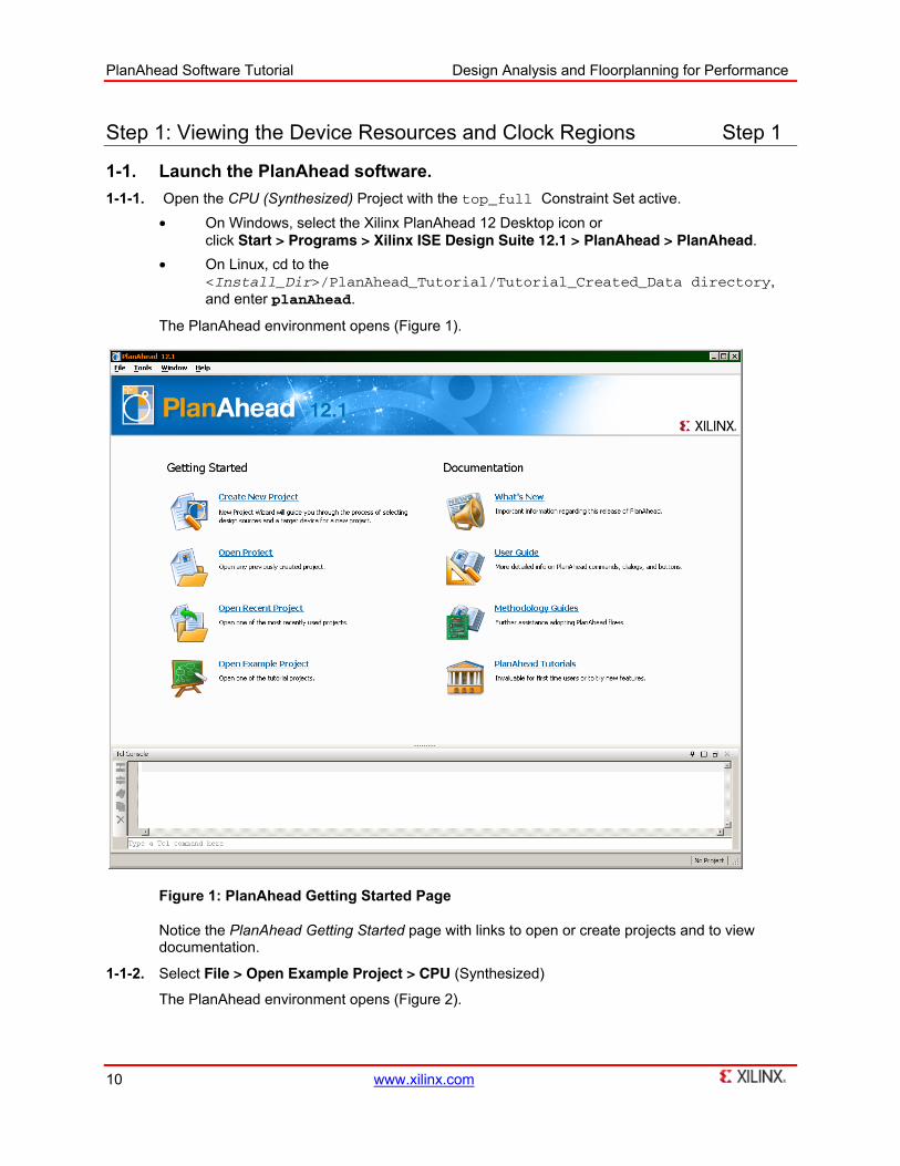
1-1. Launch the PlanAhead software. 1-1-1. Open the CPU (Synthesized) Project with the top_full Constraint Set active.
• On Windows, select the Xilinx PlanAhead 12 Desktop icon or click Start > Programs > Xilinx ISE Design Suite 12.1 > PlanAhead > PlanAhead.
• On Linux, cd to the <Install_Dir>/PlanAhead_Tutorial/Tutorial_Created_Data directory, and enter planAhead.
The PlanAhead environment opens (Figure 1).
Figure 1: PlanAhead Getting Started Page
Notice the PlanAhead Getting Started page with links to open or create projects and to view documentation.
1-1-2. Select File > Open Example Project > CPU (Synthesized)
The PlanAhead environment opens (Figure 2).

PlanAhead Software Tutorial Design Analysis and Floorplanning for Performance
www.xilinx.com 11
Figure 2: PlanAhead Environment
1-1-3. In the PlanAhead main window, ensure that the Constraints constrs_1> top_full.ucf is active (Figure 3).
Figure 3: Sources View with Constrs_1
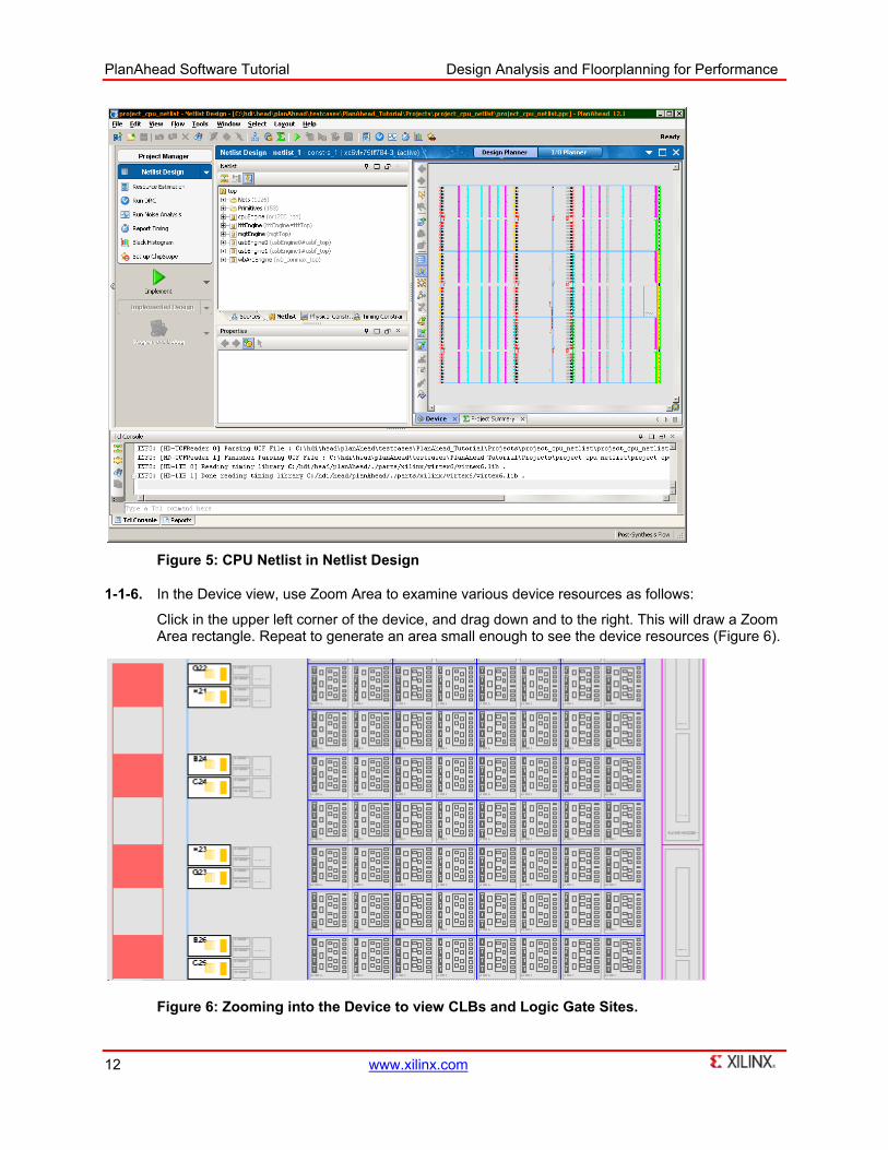
1-1-4. Open the design and constraints by clicking on Netlist Design in the Flow Navigator (Figure 4).
Figure 4: Netlist Design
1-1-5. The tool will now open the netlist and top_full.ucf as shown (Figure 5).
PlanAhead Software Tutorial Design Analysis and Floorplanning for Performance
12 www.xilinx.com
Figure 5: CPU Netlist in Netlist Design
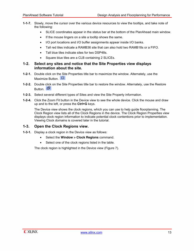
1-1-6. In the Device view, use Zoom Area to examine various device resources as follows:
Click in the upper left corner of the device, and drag down and to the right. This will draw a Zoom Area rectangle. Repeat to generate an area small enough to see the device resources (Figure 6).
Figure 6: Zooming into the Device to view CLBs and Logic Gate Sites.
PlanAhead Software Tutorial Design Analysis and Floorplanning for Performance
www.xilinx.com 13
1-1-7. Slowly, move the cursor over the various device resources to view the tooltips, and take note of the following:
• SLICE coordinates appear in the status bar at the bottom of the PlanAhead main window. • If the mouse lingers on a site a tooltip shows the same. • I/O port locations and I/O buffer assignments appear inside I/O banks. • Tall red tiles indicate a RAMB36 site that can also hold two RAMB18s or a FIFO. • Tall blue tiles indicate sites for two DSP48s. • Square blue tiles are a CLB containing 2 SLICEs.
1-2. Select any sites and notice that the Site Properties view displays information about the site.
1-2-1. Double click on the Site Properties title bar to maximize the window. Alternately, use the Maximize Button.
1-2-2. Double click on the Site Properties title bar to restore the window. Alternately, use the Restore Button.
1-2-3. Select several different types of Sites and view the Site Property information.
1-2-4. Click the Zoom Fit button in the Device view to see the whole device. Click the mouse and draw up and to the left, or press the Ctrl+G keys.
The Device view shows the clock regions, which you can use to help guide floorplanning. The Clock Region view lists all of the Clock Regions in the device. The Clock Region Properties view displays clock region information to indicate potential clock contentions prior to implementation. Viewing Clock domains is covered later in the tutorial.
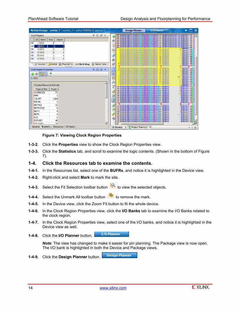
1-3. Open the Clock Regions view. 1-3-1. Display a clock region in the Device view as follows:
• Select the Window > Clock Regions command. • Select one of the clock regions listed in the table.
The clock region is highlighted in the Device view (Figure 7).
PlanAhead Software Tutorial Design Analysis and Floorplanning for Performance
14 www.xilinx.com
Figure 7: Viewing Clock Region Properties
1-3-2. Click the Properties view to show the Clock Region Properties view.
1-3-3. Click the Statistics tab, and scroll to examine the logic contents. (Shown in the bottom of Figure 7).
1-4. Click the Resources tab to examine the contents. 1-4-1. In the Resources list, select one of the BUFRs, and notice it is highlighted in the Device view.
1-4-2. Right-click and select Mark to mark the site.
1-4-3. Select the Fit Selection toolbar button to view the selected objects.
1-4-4. Select the Unmark All toolbar button to remove the mark.
1-4-5. In the Device view, click the Zoom Fit button to fit the whole device.
1-4-6. In the Clock Region Properties view, click the I/O Banks tab to examine the I/O Banks related to the clock region.
1-4-7. In the Clock Region Properties view, select one of the I/O banks, and notice it is highlighted in the Device view as well.
1-4-8. Click the I/O Planner button.
Note: The view has changed to make it easier for pin planning. The Package view is now open. The I/O bank is highlighted in both the Device and Package views.
1-4-9. Click the Design Planner button.

PlanAhead Software Tutorial Design Analysis and Floorplanning for Performance
www.xilinx.com 15
Step 2: Exploring the Logical Netlist Hierarchy Step 2
2-1. Use the Netlist view to explore the design hierarchy.
2-1-1. In the Netlist view, click the Collapse All toolbar button .
2-1-2. Click the expand widget next to cpuEngine to expand the module.
The Netlist should now look similar to the one shown below (Figure 8).
Figure 8: Expanding the Netlist View
Note: There is a Primitives folder in the Netlist view that contains the top-level instances of each module.
2-1-3. Expand the Primitives folder. These are the instances at the cpuEngine level not in any sub-module.
2-1-4. Expand the Nets folder. These are the nets inside the module.
2-1-5. In the Netlist view, click the Collapse All toolbar button.
2-2. Select netlist modules and view where the logic resides in the design hierarchy.
2-2-1. In the Netlist view, expand the usbEngine0 module.

PlanAhead Software Tutorial Design Analysis and Floorplanning for Performance
16 www.xilinx.com
2-2-2. Select the u4 module.
2-2-3. Right-click and select the Show Hierarchy command.
2-2-4. The Hierarchy view opens in the Workspace (Figure 9).
Figure 9: Displaying the Instance Hierarchy View
The Hierarchy view displays the hierarchical relationship of the modules and the relative sizes. The selected logic module displays in the Hierarchy view, which is useful to visualize the module location and relative size prior to floorplanning. You can select modules directly from this view for floorplanning. Logic selected in other views is highlighted in the Hierarchy view.
2-2-5. Select any module in the Hierarchy view, and notice it is selected in the Netlist view as well.
2-2-6. Click the Unselect All button, or press F12.
PlanAhead Software Tutorial Design Analysis and Floorplanning for Performance
www.xilinx.com 17
Step 3: Displaying Design Resources Statistics Step 3
The PlanAhead software utilization analysis provides design statistics to help determine the optimal device for the design. The tool helps the user see how the logic resources are split between modules. It is easy to explore multiple device types to determine the best overall utilization and performance estimations.
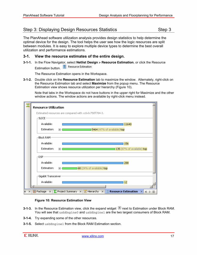
3-1. View the resource estimates of the entire design. 3-1-1. In the Flow Navigator, select Netlist Design > Resource Estimation, or click the Resource
Estimation button.
The Resource Estimation opens in the Workspace.
3-1-2. Double click on the Resource Estimation tab to maximize the window. Alternately, right-click on the Resource Estimation tab and select Maximize from the popup menu. The Resource Estimation view shows resource utilization per hierarchy (Figure 10).
Note that tabs in the Workspace do not have buttons in the upper right for Maximize and the other window actions. The window actions are available by right-click menu instead.
Figure 10: Resource Estimation View
3-1-3. In the Resource Estimation view, click the expand widget next to Estimation under Block RAM. You will see that usbEngine0 and usbEngine1 are the two largest consumers of Block RAM.
3-1-4. Try expanding some of the other resources.
3-1-5. Select usbEngine1 from the Block RAM Estimation section.
PlanAhead Software Tutorial Design Analysis and Floorplanning for Performance
18 www.xilinx.com
3-1-6. Click the Hierarchy tab.
Note: The usbEngine1 is selected in the hierarchy browser as well. Selecting something in one view selects the object in other views as well.
3-1-7. Click the Close X button to close the Hierarchy view.
3-1-8. Click the Close X button to close the Hierarchy view.
3-1-9. Select Layout > Load Layout > PlanAhead Defaults to restore the default window layout.
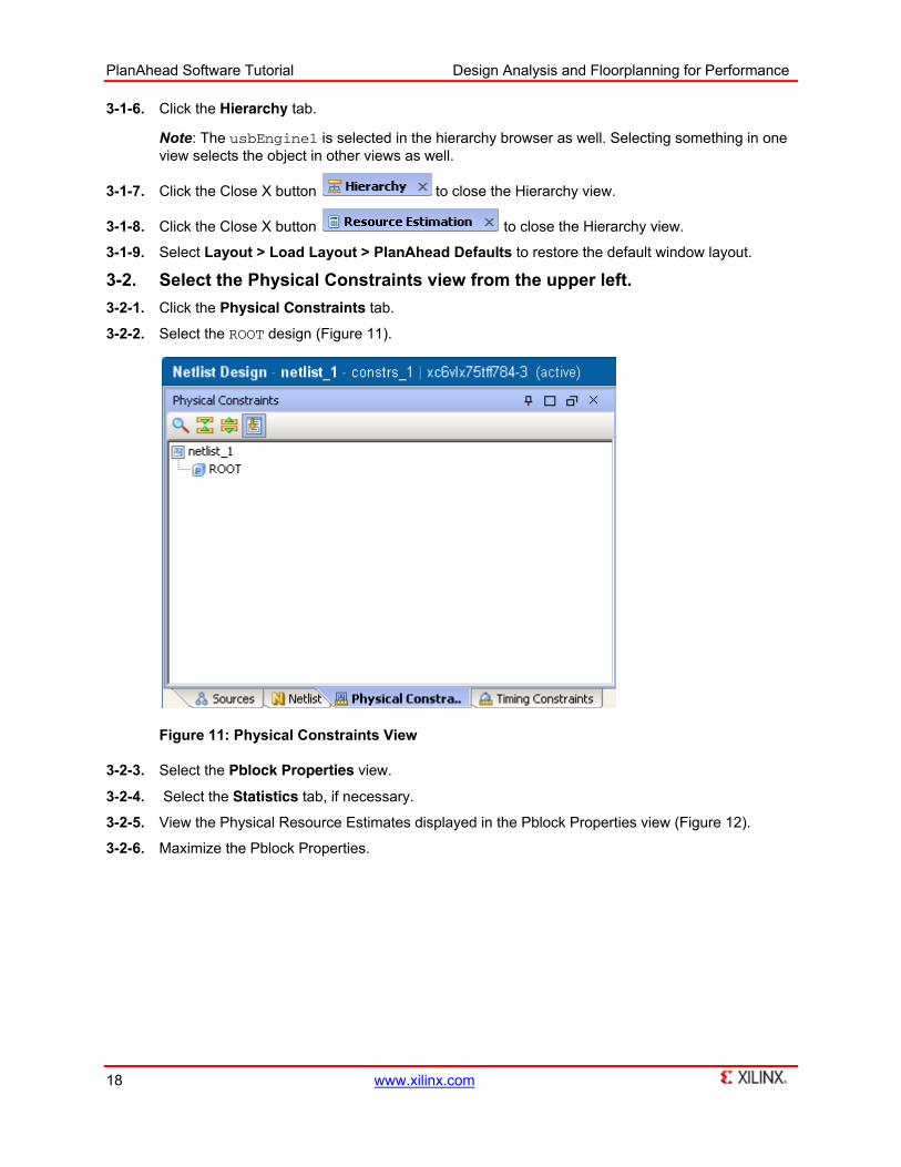
3-2. Select the Physical Constraints view from the upper left. 3-2-1. Click the Physical Constraints tab.
3-2-2. Select the ROOT design (Figure 11).
Figure 11: Physical Constraints View
3-2-3. Select the Pblock Properties view.
3-2-4. Select the Statistics tab, if necessary.
3-2-5. View the Physical Resource Estimates displayed in the Pblock Properties view (Figure 12).
3-2-6. Maximize the Pblock Properties.

PlanAhead Software Tutorial Design Analysis and Floorplanning for Performance
www.xilinx.com 19
Figure 12: Viewing Design Resource Statistics
3-2-7. Scroll through the design statistics displayed in the Pblock Properties view.
Note: The Statistics tab shows the device resource utilization for each type of logic element, carry chain count, longest length, Clock Report, IO utilization, and Primitive instance and interface net counts. If this design had any RPMs, the RPM count and maximum size information would be shown also.
3-2-8. Restore the Pblock Properties.

PlanAhead Software Tutorial Design Analysis and Floorplanning for Performance
20 www.xilinx.com
Step 4: Running Design Rule Checks (DRC) Step 4
Xilinx recommends running the Design Rule Checker before implementation.
4-1. Run the Design Rule Checker (DRC). 4-1-1. Select Tools > Run DRC.
The Run DRC dialog box appears (Figure 13).
Figure 13: Running DRC
4-1-2. Click OK to run all rule checks.
The DRC Results view opens and indicates that there are several DSP48 warnings (Figure 14).
PlanAhead Software Tutorial Design Analysis and Floorplanning for Performance
www.xilinx.com 21
Figure 14: Design Rule Violations Window
Errors, warnings and information messages appear in the DRC Results window. Errors are indicated by a red icon. Warnings are indicated by an orange icon. Information messages are indicated by a yellow icon. Even if the DRCs issue an Error, implementation may complete successfully.
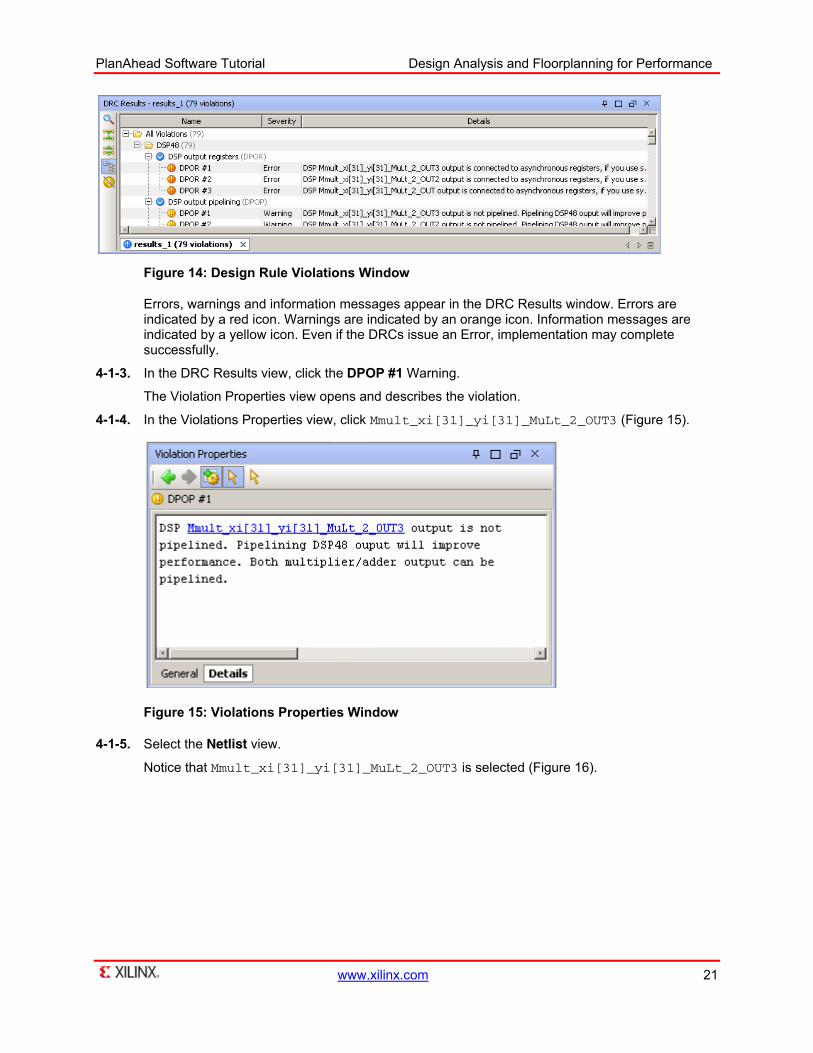
4-1-3. In the DRC Results view, click the DPOP #1 Warning.
The Violation Properties view opens and describes the violation.
4-1-4. In the Violations Properties view, click Mmult_xi[31]_yi[31]_MuLt_2_OUT3 (Figure 15).
Figure 15: Violations Properties Window
4-1-5. Select the Netlist view.
Notice that Mmult_xi[31]_yi[31]_MuLt_2_OUT3 is selected (Figure 16).

PlanAhead Software Tutorial Design Analysis and Floorplanning for Performance
22 www.xilinx.com
Figure 16: Instance in Netlist View
4-1-6. In the DRC Results view, scroll down the list of violations.
4-1-7. Close the DRC Results view by clicking the Close X button in the tab.
PlanAhead Software Tutorial Design Analysis and Floorplanning for Performance
www.xilinx.com 23
Step 5: Performing Timing Analysis Step 5
To determine the feasibility of the design’s timing constraints, perform an early static timing estimation, including estimated route delays.
5-1. Analyze timing end points in the Slack Histogram. The tool will bin the end points based on slack and present a histogram. It is possible to visualize how many end points are tight on timing versus those that have a margin.
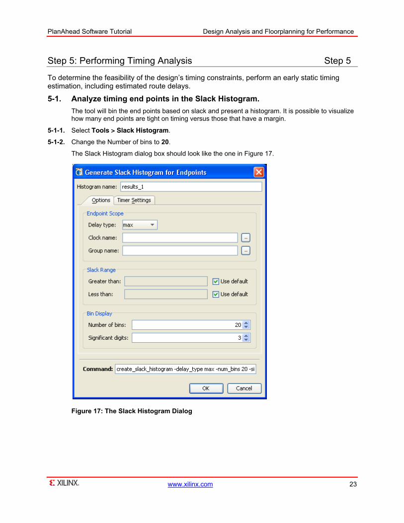
5-1-1. Select Tools > Slack Histogram.
5-1-2. Change the Number of bins to 20.
The Slack Histogram dialog box should look like the one in Figure 17.
Figure 17: The Slack Histogram Dialog

PlanAhead Software Tutorial Design Analysis and Floorplanning for Performance
24 www.xilinx.com
5-2. Click the Timer Settings tab. 5-2-1. Inspect the settings.
Note: The Timer Settings tab lets you change how the tool accounts for route delay. The timer can estimate route delay or assume there is no interconnect routing delay.
5-2-2. Click OK.
A histogram will display showing binned end points (Figure 18).
Figure 18: Slack Histogram
5-2-3. Click on various bins.
Note: The end points in the lower view filter as the bins are selected. The slack range is also updated.
5-2-4. Select the left most bin, which is the bin with the least timing margin.
5-2-5. Inspect the end points.
Note: Most of the timing end points are Block RAMs in the two usbEngine blocks.
5-2-6. Select an instance from the filtered histogram report. It cross selects in the netlist view.
5-2-7. Click the Close X button to close the histogram .

PlanAhead Software Tutorial Design Analysis and Floorplanning for Performance
www.xilinx.com 25
5-3. Analyze the results and information in the Timing Results view. 5-3-1. Select Tools > Report Timing.
The Report Timing dialog box opens (Figure 19) to the Targets tab, which enables you to specify timing start and end points.
Figure 19: Running TimeAhead Timing Analysis.

PlanAhead Software Tutorial Design Analysis and Floorplanning for Performance
26 www.xilinx.com
5-4. Switch to the Options tab (Figure 20).
Figure 20: Report Timing Options Tab
5-4-1. In the Number of paths per group field, type 30.
5-4-2. Click the Advanced and Timer Settings and inspect the tabs. Do not change anything.
5-4-3. Click OK to run analysis.
The Timing Results view opens (Figure 21).
Figure 21: Analyzing Timing Analysis Results

PlanAhead Software Tutorial Design Analysis and Floorplanning for Performance
www.xilinx.com 27
The list of paths display in the report. The report shows Path Type, Slack, Source, Destination, Total Delay, Logic Delay, Net Delay Percentage, Stages of logic, start clock, and destination clock. Failing paths appear in red.
5-4-4. Maximize the Timing Results view.
5-4-5. Scroll down the list of paths.
Note: The From and To values are in one of the usbEngine modules.
5-4-6. Click the To column header twice to sort the list by Source.The report is now reverse sorted by To column values.
Note: You can sort all of the table style views in the PlanAhead software in the same way.
• To perform a reverse sort, click the column header again.
• To perform a secondary sort, press the Ctrl key and select another column header.
5-4-7. Restore the Timing Results view.
5-4-8. Select the Path 1 in the list.
PlanAhead Software Tutorial Design Analysis and Floorplanning for Performance
28 www.xilinx.com
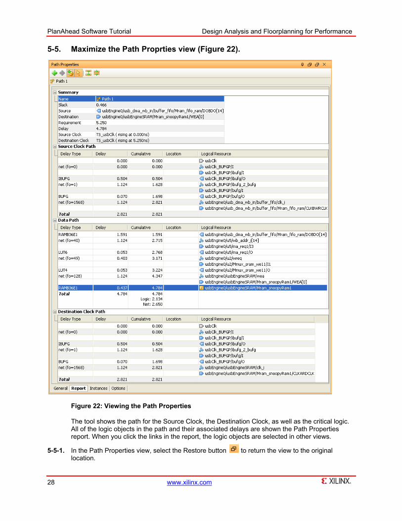
5-5. Maximize the Path Proprties view (Figure 22).
Figure 22: Viewing the Path Properties
The tool shows the path for the Source Clock, the Destination Clock, as well as the critical logic. All of the logic objects in the path and their associated delays are shown the Path Properties report. When you click the links in the report, the logic objects are selected in other views.
5-5-1. In the Path Properties view, select the Restore button to return the view to the original location.
PlanAhead Software Tutorial Design Analysis and Floorplanning for Performance
www.xilinx.com 29
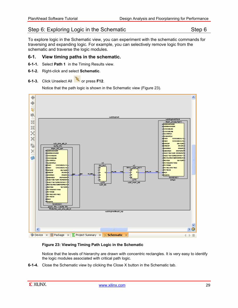
Step 6: Exploring Logic in the Schematic Step 6
To explore logic in the Schematic view, you can experiment with the schematic commands for traversing and expanding logic. For example, you can selectively remove logic from the schematic and traverse the logic modules.
6-1. View timing paths in the schematic. 6-1-1. Select Path 1 in the Timing Results view.
6-1-2. Right-click and select Schematic.
6-1-3. Click Unselect All or press F12.
Notice that the path logic is shown in the Schematic view (Figure 23).
Figure 23: Viewing Timing Path Logic in the Schematic
Notice that the levels of hierarchy are drawn with concentric rectangles. It is very easy to identify the logic modules associated with critical path logic.
6-1-4. Close the Schematic view by clicking the Close X button in the Schematic tab.

PlanAhead Software Tutorial Design Analysis and Floorplanning for Performance
30 www.xilinx.com
6-1-5. Press the Shift keys and select all of the paths in the Timing Results view that have a From value beginning with usbEngine0/…
6-1-6. Right-click and select Schematic.
All of the logic associated with each selected path displays and is selected in the Schematic view (Figure 24).
Figure 24: Viewing Multiple Timing Paths in the Schematic
6-1-7. In the Netlist view, click the Collapse All toolbar button .
6-1-8. With the group of paths still selected and the cursor in the Schematic view, right-click and select Select Primitive Parents.
The four modules with the path logic are highlighted in the Netlist view.
PlanAhead Software Tutorial Design Analysis and Floorplanning for Performance
www.xilinx.com 31
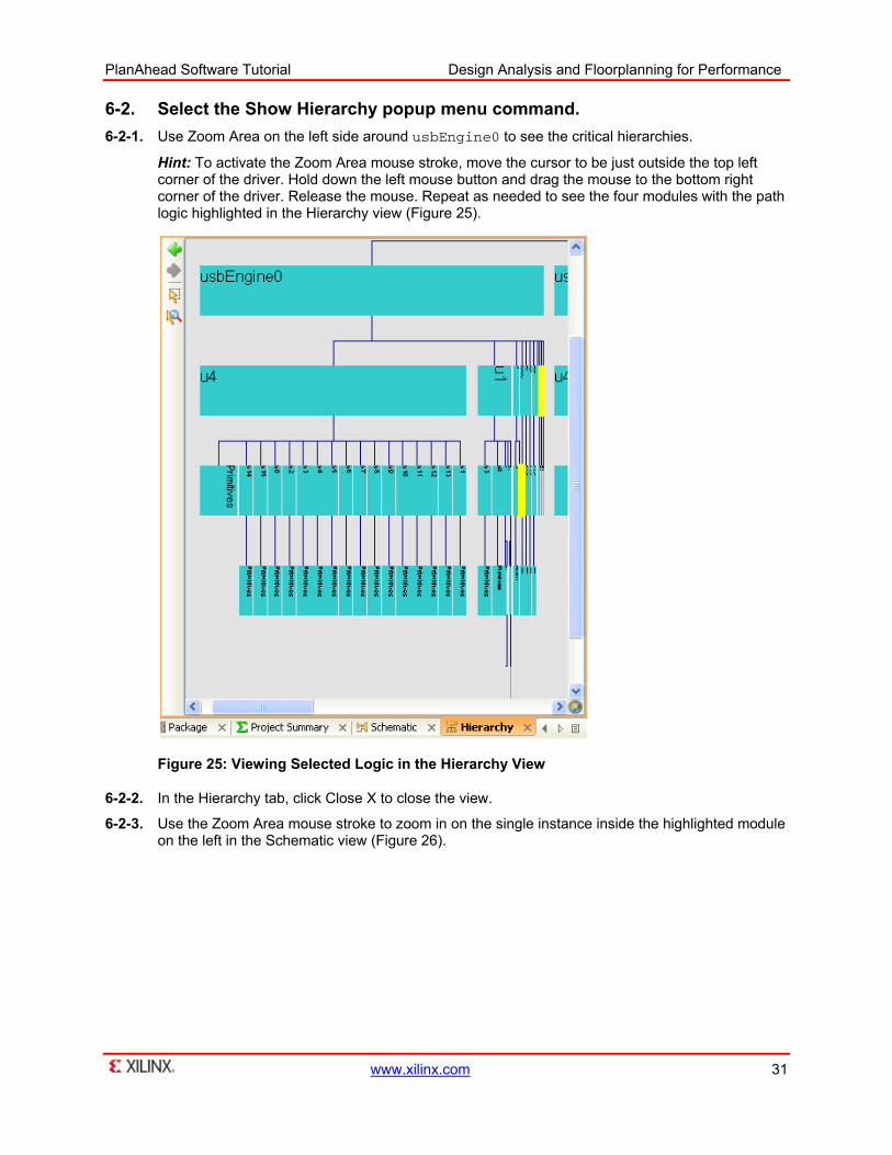
6-2. Select the Show Hierarchy popup menu command. 6-2-1. Use Zoom Area on the left side around usbEngine0 to see the critical hierarchies.
Hint: To activate the Zoom Area mouse stroke, move the cursor to be just outside the top left corner of the driver. Hold down the left mouse button and drag the mouse to the bottom right corner of the driver. Release the mouse. Repeat as needed to see the four modules with the path logic highlighted in the Hierarchy view (Figure 25).
Figure 25: Viewing Selected Logic in the Hierarchy View
6-2-2. In the Hierarchy tab, click Close X to close the view.
6-2-3. Use the Zoom Area mouse stroke to zoom in on the single instance inside the highlighted module on the left in the Schematic view (Figure 26).

PlanAhead Software Tutorial Design Analysis and Floorplanning for Performance
32 www.xilinx.com
Figure 26: Critical Path Source
6-2-4. Select the RAMB36E1.
6-2-5. Click the Collapse Outside button .
6-2-6. Click the Unselect All button or press F12.
6-2-7. Double-click the ADDRARDADDR pin and notice that the logic connected to it is expanded (Figure 27).

PlanAhead Software Tutorial Design Analysis and Floorplanning for Performance
www.xilinx.com 33
Figure 27: Interactively Expanding Logic in the Schematic View
6-2-8. Double-click wr_addr_0. This adds the logic to which it connects to the schematic.
6-2-9. In the Schematic view, select the Previous schematic button .
You can use the Previous schematic and Next schematic toolbar buttons to browse the various views displayed in the Schematic view. This enables you to toggle the various levels of schematic expansion.
Note: The Edit > Undo command is not available while interactively expanding the schematic logic.
6-2-10. Select the smaller buffer_fifo module hierarchical rectangle containing the RAMB36E1 instance.
6-2-11. In the Schematic view, click the Expand Inside button .
6-2-12. Zoom Fit in the schematic (Figure 28).

PlanAhead Software Tutorial Design Analysis and Floorplanning for Performance
34 www.xilinx.com
Figure 28: Expanding Logic Inside of Schematic Modules.
6-2-13. Click the Select Area toolbar button and draw a rectangle around some of the logic in the Schematic view.
6-2-14. Click the Remove selected elements from schematic toolbar button . Notice that some logic is no longer displayed.
6-2-15. Click the Close X button to close the Schematic view.
6-2-16. In the Netlist view, click the Collapse All button .
Note: This tutorial covers only a subset of the Schematic view commands and options for traversing the logic.

PlanAhead Software Tutorial Design Analysis and Floorplanning for Performance
www.xilinx.com 35
Step 7: Modifying the Design Timing Constraints Step 7
7-1. Modify the properties of the TS_cpuClk constraints to change the 13.75 ns target to 12.75 ns.
7-1-1. Click the Timing Constraints view next to the Netlist View (Figure 29).
Figure 29: Timing Constraints View
7-1-2. Click the Expand All button to expand the timing constraints.
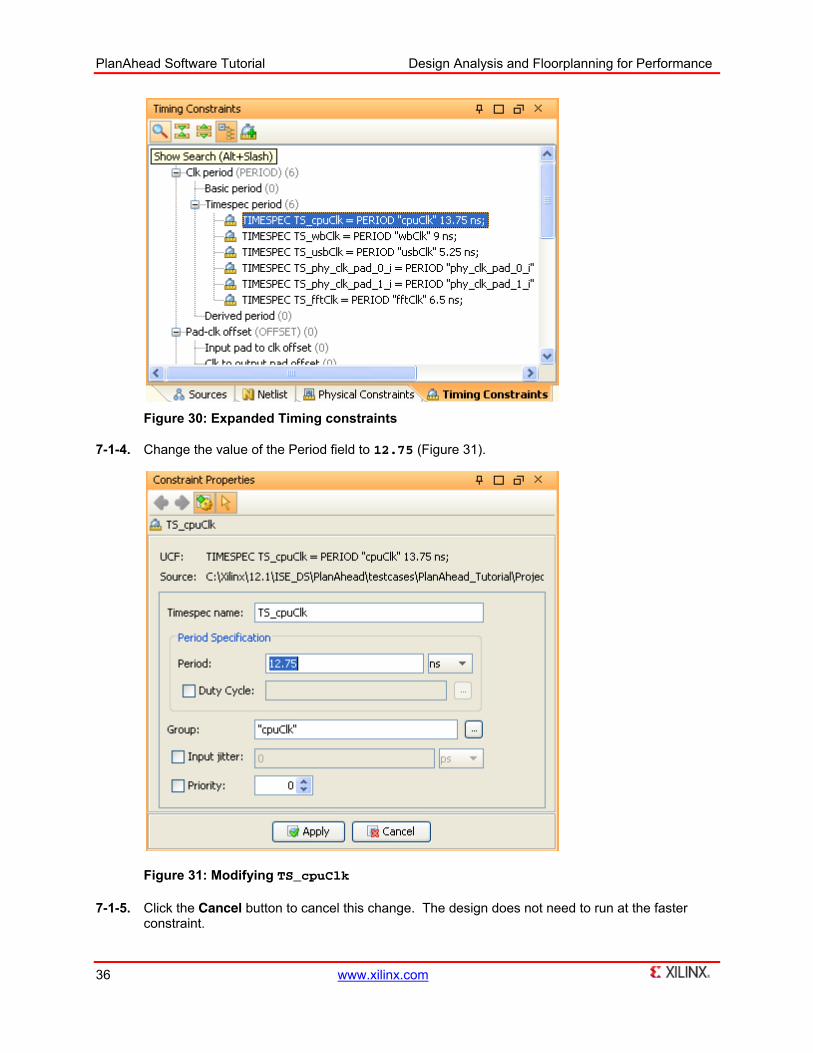
7-1-3. Select the TIMESPEC TS_cpuClk constraint (Figure 30). The Constraints Properties window displays.
Note: The TIMESPEC is a sub group of Clock Period and Timespec Period. By default, the tool groups constraints by type.
PlanAhead Software Tutorial Design Analysis and Floorplanning for Performance
36 www.xilinx.com
Figure 30: Expanded Timing constraints
7-1-4. Change the value of the Period field to 12.75 (Figure 31).
Figure 31: Modifying TS_cpuClk
7-1-5. Click the Cancel button to cancel this change. The design does not need to run at the faster constraint.
PlanAhead Software Tutorial Design Analysis and Floorplanning for Performance
www.xilinx.com 37
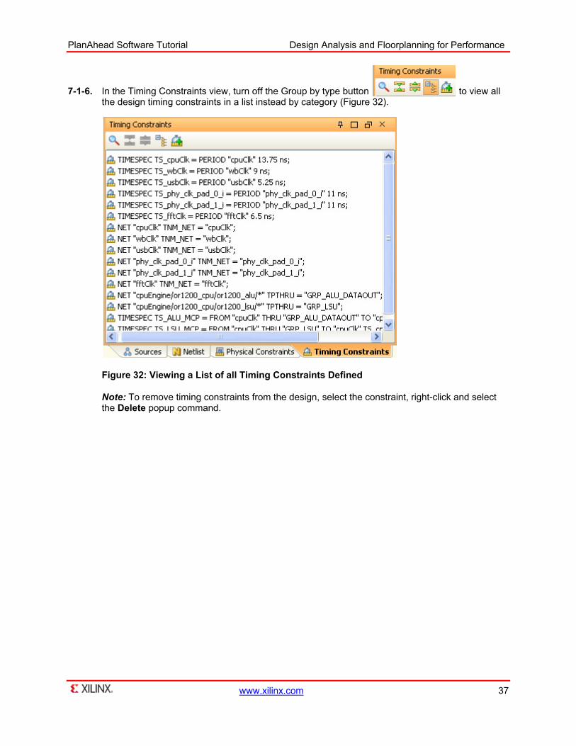
7-1-6. In the Timing Constraints view, turn off the Group by type button to view all the design timing constraints in a list instead by category (Figure 32).
Figure 32: Viewing a List of all Timing Constraints Defined
Note: To remove timing constraints from the design, select the constraint, right-click and select the Delete popup command.
PlanAhead Software Tutorial Design Analysis and Floorplanning for Performance
38 www.xilinx.com
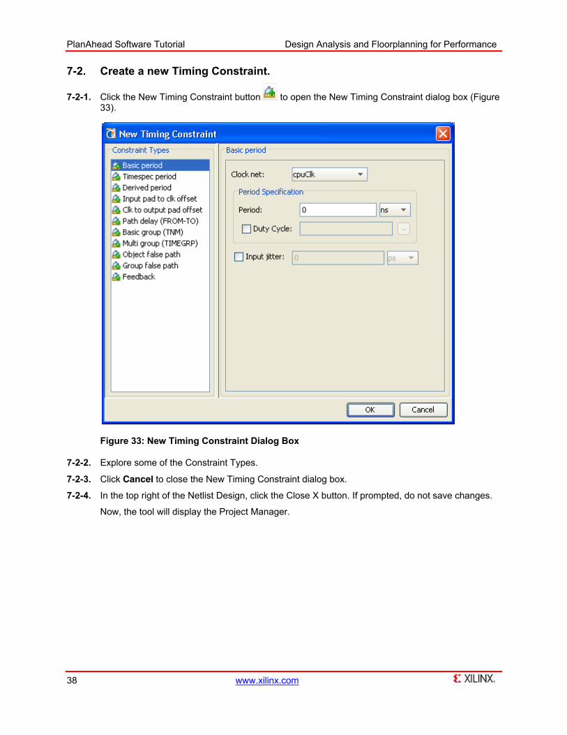
7-2. Create a new Timing Constraint.
7-2-1. Click the New Timing Constraint button to open the New Timing Constraint dialog box (Figure 33).
Figure 33: New Timing Constraint Dialog Box
7-2-2. Explore some of the Constraint Types.
7-2-3. Click Cancel to close the New Timing Constraint dialog box.
7-2-4. In the top right of the Netlist Design, click the Close X button. If prompted, do not save changes.
Now, the tool will display the Project Manager.
PlanAhead Software Tutorial Design Analysis and Floorplanning for Performance
www.xilinx.com 39
Step 8: Implementing the Design Step 8
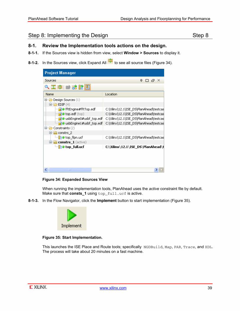
8-1. Review the Implementation tools actions on the design. 8-1-1. If the Sources view is hidden from view, select Window > Sources to display it.
8-1-2. In the Sources view, click Expand All to see all source files (Figure 34).
Figure 34: Expanded Sources View
When running the implementation tools, PlanAhead uses the active constraint file by default. Make sure that consts_1 using top_full.ucf is active.
8-1-3. In the Flow Navigator, click the Implement button to start implementation (Figure 35).
Figure 35: Start Implementation.
This launches the ISE Place and Route tools; specifically NGDBuild, Map, PAR, Trace, and XDL. The process will take about 20 minutes on a fast machine.
PlanAhead Software Tutorial Design Analysis and Floorplanning for Performance
40 www.xilinx.com
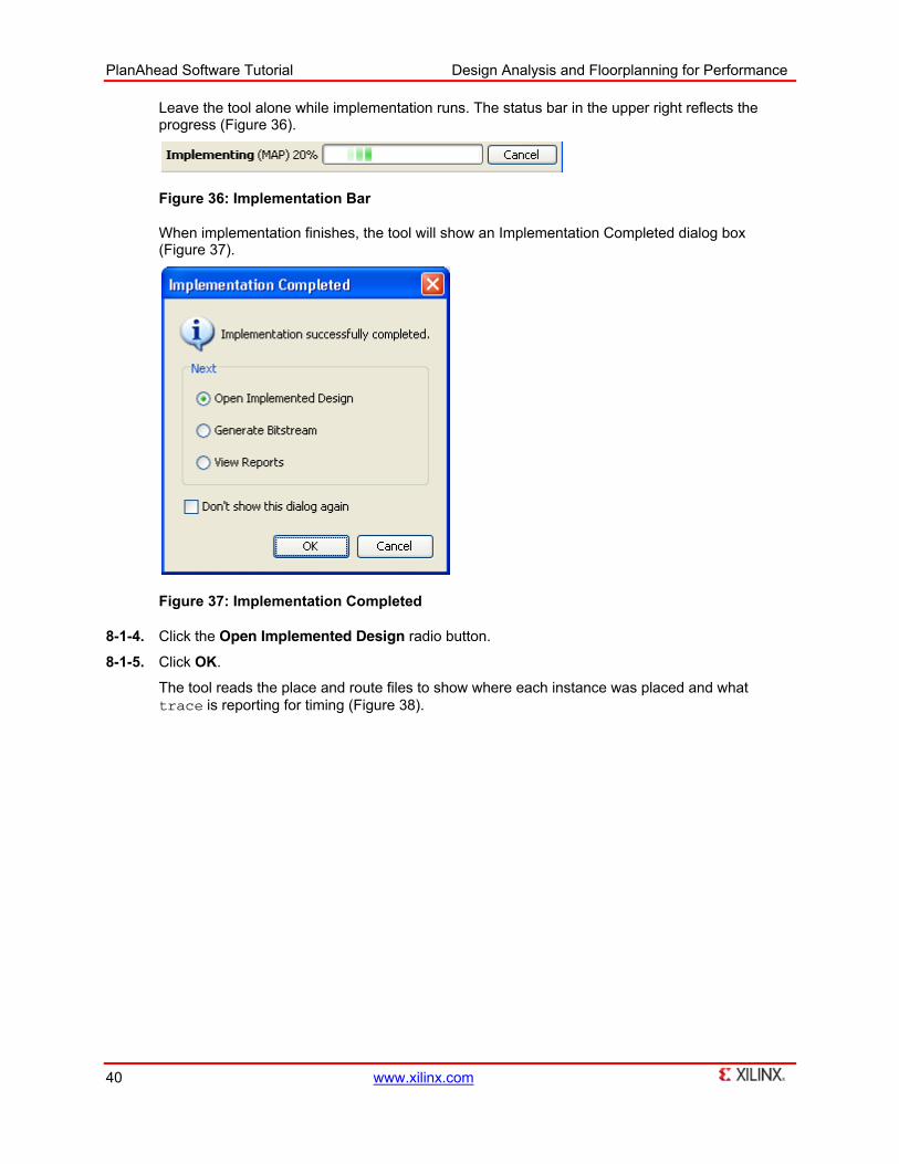
Leave the tool alone while implementation runs. The status bar in the upper right reflects the progress (Figure 36).
Figure 36: Implementation Bar
When implementation finishes, the tool will show an Implementation Completed dialog box (Figure 37).
Figure 37: Implementation Completed
8-1-4. Click the Open Implemented Design radio button.
8-1-5. Click OK.
The tool reads the place and route files to show where each instance was placed and what trace is reporting for timing (Figure 38).

PlanAhead Software Tutorial Design Analysis and Floorplanning for Performance
www.xilinx.com 41
Figure 38: The Implemented Design
8-1-6. Double-click the Compilation Messages title bar to maximize the Compilation Messages view.
8-1-7. Click the Expand widget by Place and Route to see the messages generated at this step (Figure 39).
Figure 39: Compilation Messages
Note: The Compilation Messages view collects all information, warning, and error messages generated by the implementation tools. Click the Blue Circle to hide Information messages. Click the Yellow Circle to hide Warnings.
8-1-8. Double-click the Compilation Messages title bar to restore the view.

PlanAhead Software Tutorial Design Analysis and Floorplanning for Performance
42 www.xilinx.com
Step 9: Analyzing the Timing Results Step 9
You can analyze timing results from implementation to drive the floorplanning effort. You can use the path sorting and selection techniques available in the Timing Results view with imported TRACE report data.
9-1. Explore the Implementation timing results. 9-1-1. Double-click the top blue bar labeled Implemented Design – impl_1 to maximize the work area.
9-1-2. In the Timing Results view, select Path 1 (Figure 40).
9-1-3. Right-click and select the Mark popup command.
Figure 40: Selecting the Most Critical Timing Path
Imported timing results sort the timing paths on a constraint-by-constraint basis. When you select paths in the Timing Results view, the Path properties view shows the details of the timing path.
Because the placement was imported, the path is highlighted in the Device view. The visualization makes it easy to understand how to take appropriate floorplanning steps to improve the timing.
After running the Mark command, the red and green stars show the timing path start and end points (Figure 41).

PlanAhead Software Tutorial Design Analysis and Floorplanning for Performance
www.xilinx.com 43
Figure 41: Placement of the Timing Path
9-1-4. Select Select > Unmark All to clear the marks.
9-1-5. Press Shift and select all of the failing paths in TS_usbClk. Do not grab paths from other timing constraints.
9-1-6. Right-click and select the Schematic popup menu command.
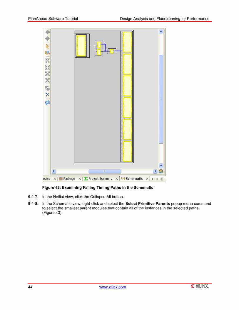
The Schematic view shows all of the instances on the selected paths (Figure 42).
PlanAhead Software Tutorial Design Analysis and Floorplanning for Performance
44 www.xilinx.com
Figure 42: Examining Failing Timing Paths in the Schematic
9-1-7. In the Netlist view, click the Collapse All button.
9-1-8. In the Schematic view, right-click and select the Select Primitive Parents popup menu command to select the smallest parent modules that contain all of the instances in the selected paths (Figure 43).
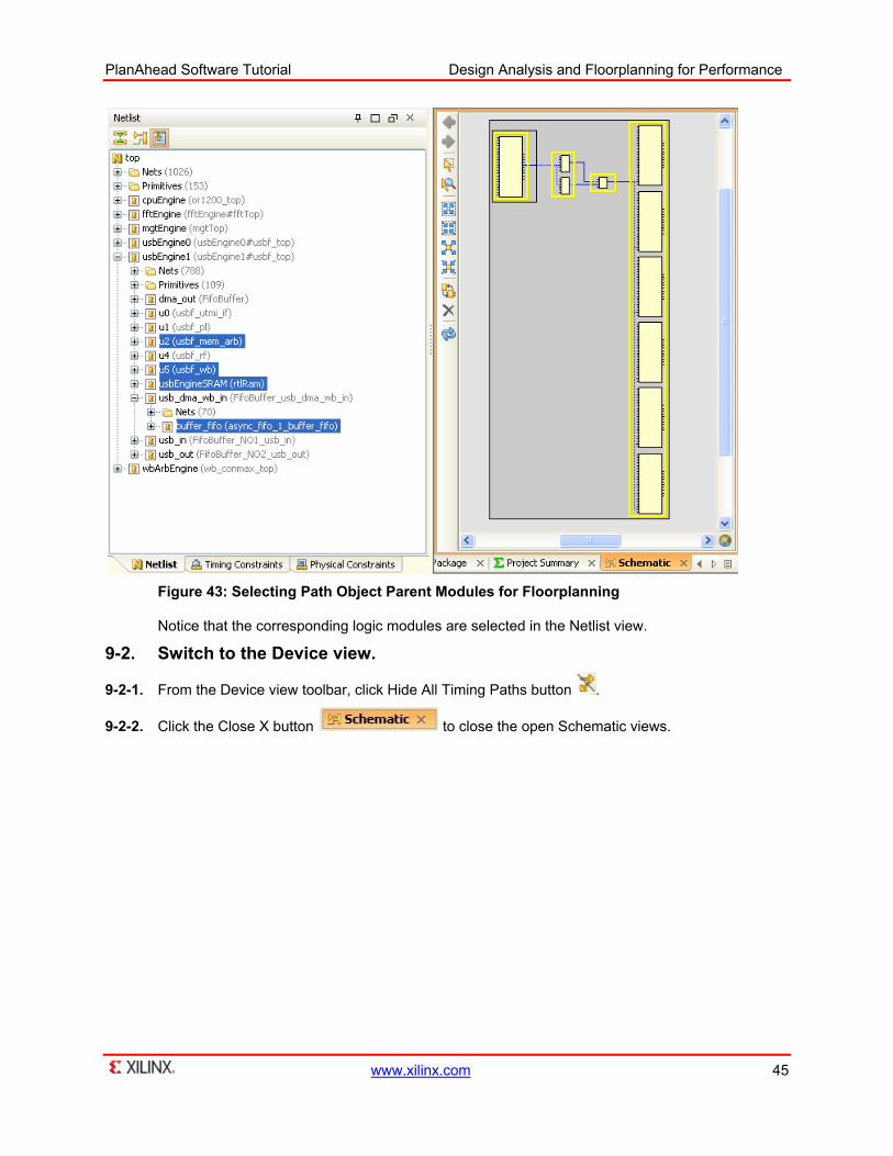
PlanAhead Software Tutorial Design Analysis and Floorplanning for Performance
www.xilinx.com 45
Figure 43: Selecting Path Object Parent Modules for Floorplanning
Notice that the corresponding logic modules are selected in the Netlist view.
9-2. Switch to the Device view.
9-2-1. From the Device view toolbar, click Hide All Timing Paths button .
9-2-2. Click the Close X button to close the open Schematic views.
PlanAhead Software Tutorial Design Analysis and Floorplanning for Performance
46 www.xilinx.com
Step 10: Highlighting Module Level Placement Step 10
You can determine a floorplanning strategy by examining previous implementation results. You can analyze module placement and guide Pblock locations by understanding how the logic was implemented without floorplanning.
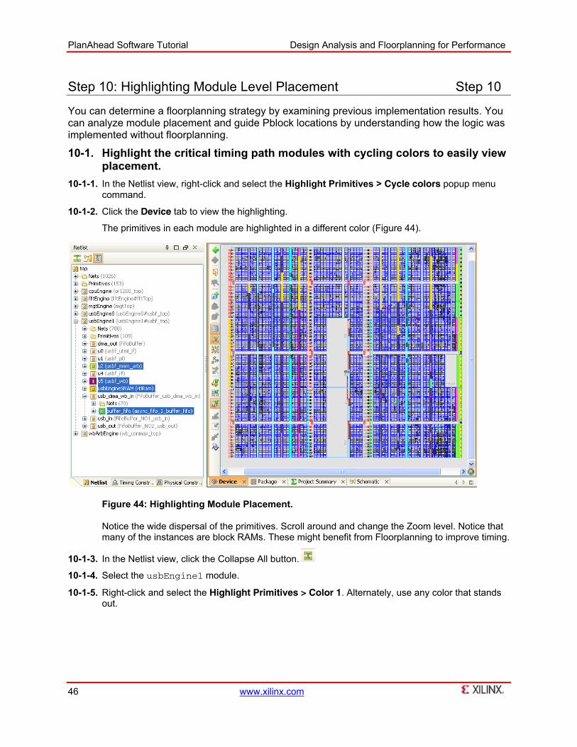
10-1. Highlight the critical timing path modules with cycling colors to easily view placement.
10-1-1. In the Netlist view, right-click and select the Highlight Primitives > Cycle colors popup menu command.
10-1-2. Click the Device tab to view the highlighting.
The primitives in each module are highlighted in a different color (Figure 44).
Figure 44: Highlighting Module Placement.
Notice the wide dispersal of the primitives. Scroll around and change the Zoom level. Notice that many of the instances are block RAMs. These might benefit from Floorplanning to improve timing.
10-1-3. In the Netlist view, click the Collapse All button.
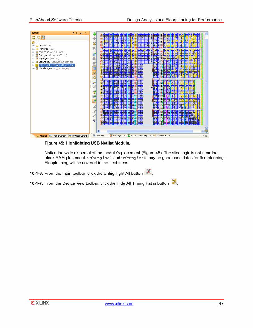
10-1-4. Select the usbEngine1 module.
10-1-5. Right-click and select the Highlight Primitives > Color 1. Alternately, use any color that stands out.
PlanAhead Software Tutorial Design Analysis and Floorplanning for Performance
www.xilinx.com 47
Figure 45: Highlighting USB Netlist Module.
Notice the wide dispersal of the module’s placement (Figure 45). The slice logic is not near the block RAM placement. usbEngine1 and usbEngine0 may be good candidates for floorplanning. Flooplanning will be covered in the next steps.
10-1-6. From the main toolbar, click the Unhighlight All button .
10-1-7. From the Device view toolbar, click the Hide All Timing Paths button .
PlanAhead Software Tutorial Design Analysis and Floorplanning for Performance
48 www.xilinx.com
Step 11: Exploring Connectivity Step 11
The PlanAhead software has extensive logic expansion, selection and highlighting capabilities. These capabilities can be used to validate that modules are suitable to floorplan. For example, logic modules that connect to logic throughout the device may not be suitable for floorplanning, while tightly grouped and self-contained modules are suitable.
Routing congestion and timing inconsistency can be alleviated by floorplanning logic outside of the critical logic areas, preventing logic from migrating into the critical areas.
11-1. Visualize the I/O Connectivity.
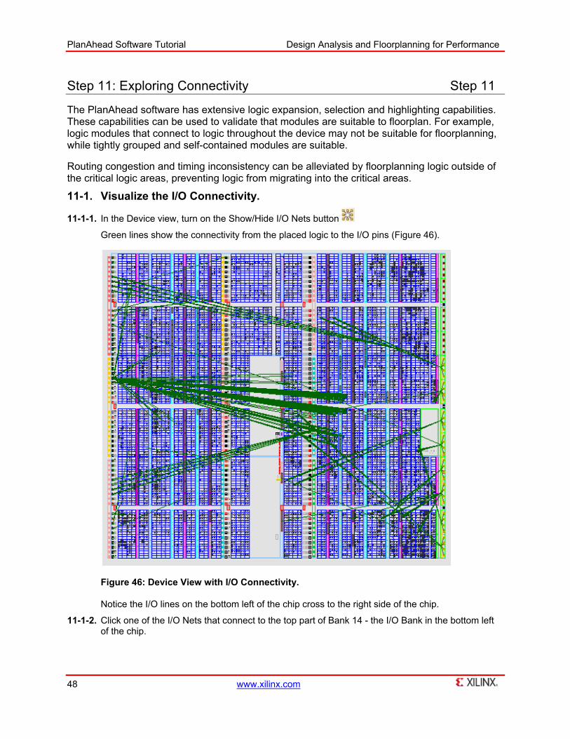
11-1-1. In the Device view, turn on the Show/Hide I/O Nets button
Green lines show the connectivity from the placed logic to the I/O pins (Figure 46).
Figure 46: Device View with I/O Connectivity.
Notice the I/O lines on the bottom left of the chip cross to the right side of the chip.
11-1-2. Click one of the I/O Nets that connect to the top part of Bank 14 - the I/O Bank in the bottom left of the chip.
PlanAhead Software Tutorial Design Analysis and Floorplanning for Performance
www.xilinx.com 49
11-1-3. Inspect the Netlist view.
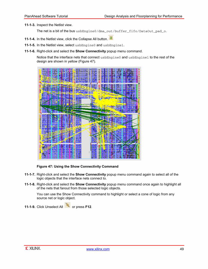
The net is a bit of the bus usbEngine0/dma_out/buffer_fifo/DataOut_pad_o.
11-1-4. In the Netlist view, click the Collapse All button.
11-1-5. In the Netlist view, select usbEngine0 and usbEngine1.
11-1-6. Right-click and select the Show Connectivity popup menu command.
Notice that the interface nets that connect usbEngine0 and usbEngine1 to the rest of the design are shown in yellow (Figure 47).
Figure 47: Using the Show Connectivity Command
11-1-7. Right-click and select the Show Connectivity popup menu command again to select all of the logic objects that the interface nets connect to.
11-1-8. Right-click and select the Show Connectivity popup menu command once again to highlight all of the nets that fanout from those selected logic objects.
You can use the Show Connectivity command to highlight or select a cone of logic from any source net or logic object.
11-1-9. Click Unselect All or press F12.

PlanAhead Software Tutorial Design Analysis and Floorplanning for Performance
50 www.xilinx.com
Step 12: Using Placement Constraints Step 12
The tool has features that allow handling of placed objects. You can view or remove placement constraints based on primitive type.
12-1. Viewing Placed Instances. 12-1-1. Select Edit > Find.
12-1-2. Change the Primitive field to Block RAM (Figure 48).
Figure 48: Find Dialog
12-1-3. Select OK.
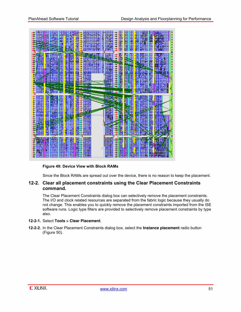
12-1-4. Select a Block Ram in the Find Results view.
12-1-5. Use the Shift key and select, or press Ctrl+A keys to select all block RAMs.
The Device view will have all the block RAMs selected (Figure 49).
PlanAhead Software Tutorial Design Analysis and Floorplanning for Performance
www.xilinx.com 51
Figure 49: Device View with Block RAMs
Since the Block RAMs are spread out over the device, there is no reason to keep the placement.
12-2. Clear all placement constraints using the Clear Placement Constraints command. The Clear Placement Constraints dialog box can selectively remove the placement constraints. The I/O and clock related resources are separated from the fabric logic because they usually do not change. This enables you to quickly remove the placement constraints imported from the ISE software runs. Logic type filters are provided to selectively remove placement constraints by type also.
12-2-1. Select Tools > Clear Placement.
12-2-2. In the Clear Placement Constraints dialog box, select the Instance placement radio button (Figure 50).

PlanAhead Software Tutorial Design Analysis and Floorplanning for Performance
52 www.xilinx.com
Figure 50: Clearing Placement Constraints
12-2-3. Click Next to display the Unplace Instances page.
12-2-4. Select Unplace All instances.
12-2-5. Click Next to display the Instance Types to Unplace page.
12-2-6. Click Default to use the Default selection.
Notice the configurable filters is available to selectively clear or keep logic LOC constraints by type.
12-3. Click Next to display the Fixed Placement page. 12-3-1. Select Keep 17 Fixed Instances.
12-3-2. Click Next to display the Clear Placement Summary page.
12-3-3. Click Finish after reviewing the Summary page.
12-3-4. In the Netlist view, click the Collapse All button .
PlanAhead Software Tutorial Design Analysis and Floorplanning for Performance
www.xilinx.com 53
Step 13: Viewing Hierarchical Connectivity Step 13
It can be useful to look at the connectivity between the modules of the netlist. In this section, you will use various tools to show the design connectivity. The netlist hierarchy will be broken apart into a physical hierarchy – called a Pblock. The Pblock will be placed on chip. The Pblock is saved into the constraints files as an AREA_GROUP constraint.
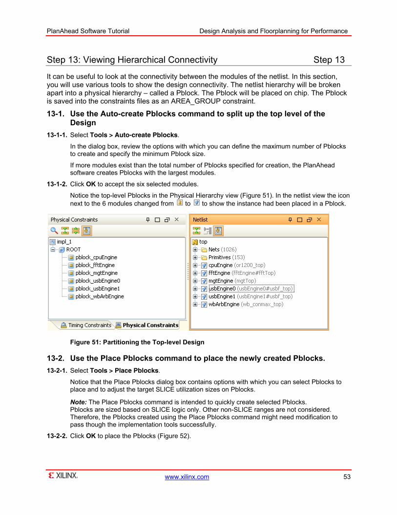
13-1. Use the Auto-create Pblocks command to split up the top level of the Design
13-1-1. Select Tools > Auto-create Pblocks.
In the dialog box, review the options with which you can define the maximum number of Pblocks to create and specify the minimum Pblock size.
If more modules exist than the total number of Pblocks specified for creation, the PlanAhead software creates Pblocks with the largest modules.
13-1-2. Click OK to accept the six selected modules.
Notice the top-level Pblocks in the Physical Hierarchy view (Figure 51). In the netlist view the icon next to the 6 modules changed from to to show the instance had been placed in a Pblock.
Figure 51: Partitioning the Top-level Design
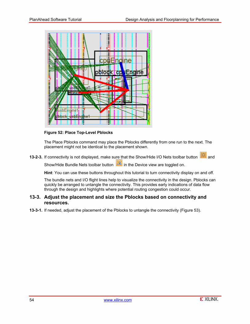
13-2. Use the Place Pblocks command to place the newly created Pblocks. 13-2-1. Select Tools > Place Pblocks.
Notice that the Place Pblocks dialog box contains options with which you can select Pblocks to place and to adjust the target SLICE utilization sizes on Pblocks.
Note: The Place Pblocks command is intended to quickly create selected Pblocks. Pblocks are sized based on SLICE logic only. Other non-SLICE ranges are not considered. Therefore, the Pblocks created using the Place Pblocks command might need modification to pass though the implementation tools successfully.
13-2-2. Click OK to place the Pblocks (Figure 52).
PlanAhead Software Tutorial Design Analysis and Floorplanning for Performance
54 www.xilinx.com
Figure 52: Place Top-Level Pblocks
The Place Pblocks command may place the Pblocks differently from one run to the next. The placement might not be identical to the placement shown.
13-2-3. If connectivity is not displayed, make sure that the Show/Hide I/O Nets toolbar button and
Show/Hide Bundle Nets toolbar button in the Device view are toggled on.
Hint: You can use these buttons throughout this tutorial to turn connectivity display on and off.
The bundle nets and I/O flight lines help to visualize the connectivity in the design. Pblocks can quickly be arranged to untangle the connectivity. This provides early indications of data flow through the design and highlights where potential routing congestion could occur.
13-3. Adjust the placement and size the Pblocks based on connectivity and resources.
13-3-1. If needed, adjust the placement of the Pblocks to untangle the connectivity (Figure 53).
PlanAhead Software Tutorial Design Analysis and Floorplanning for Performance
www.xilinx.com 55
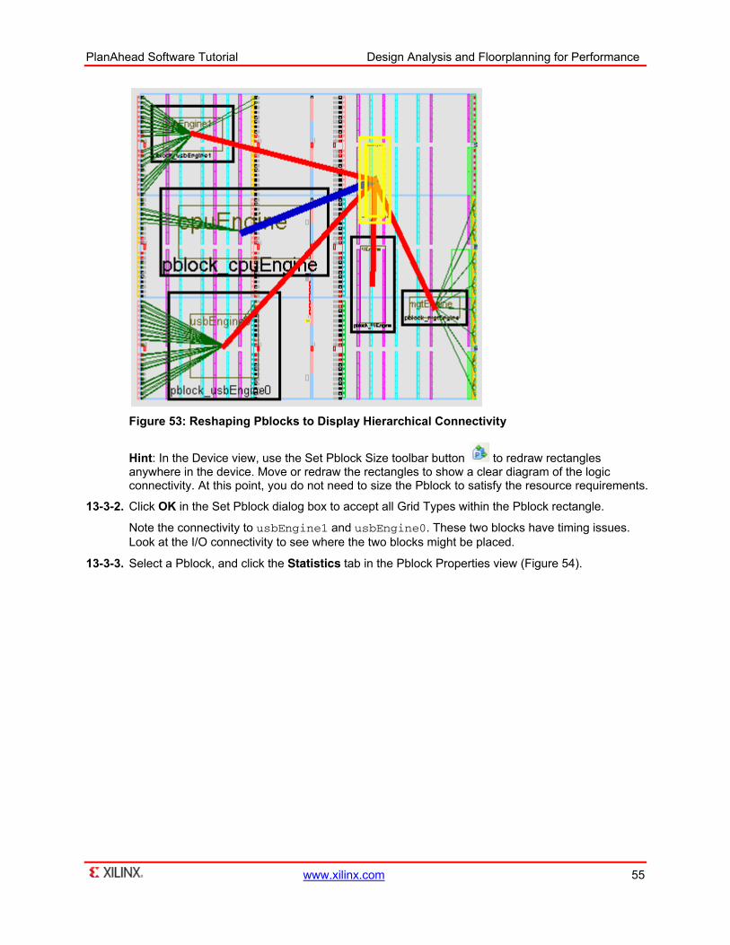
Figure 53: Reshaping Pblocks to Display Hierarchical Connectivity
Hint: In the Device view, use the Set Pblock Size toolbar button to redraw rectangles anywhere in the device. Move or redraw the rectangles to show a clear diagram of the logic connectivity. At this point, you do not need to size the Pblock to satisfy the resource requirements.
13-3-2. Click OK in the Set Pblock dialog box to accept all Grid Types within the Pblock rectangle.
Note the connectivity to usbEngine1 and usbEngine0. These two blocks have timing issues. Look at the I/O connectivity to see where the two blocks might be placed.
13-3-3. Select a Pblock, and click the Statistics tab in the Pblock Properties view (Figure 54).

PlanAhead Software Tutorial Design Analysis and Floorplanning for Performance
56 www.xilinx.com
Figure 54: Sizing Pblocks Based on Resource Estimation
Notice the Physical Resource Estimates for the Pblock. You can use these resources when sizing Pblocks to ensure adequate resources exist within the Pblock rectangle in order to accommodate the logic to which it is assigned.
13-3-4. Scroll down the list of Pblock Property Statistics.
It is often easier to create floorplans and manipulate Pblocks when certain objects are made non-selectable, such as IO nets, bundle nets and instances.
13-4. Set the View Options to make some objects not selectable. 13-4-1. Select Tools > Options.
13-4-2. In the PlanAhead Options dialog box, click the Themes category on the left to show the color Themes options.
13-4-3. At the bottom of the dialog box, click the Device tab.
13-4-4. In the Select column, deselect the Assigned Instance and IO Net object types (Figure 55).
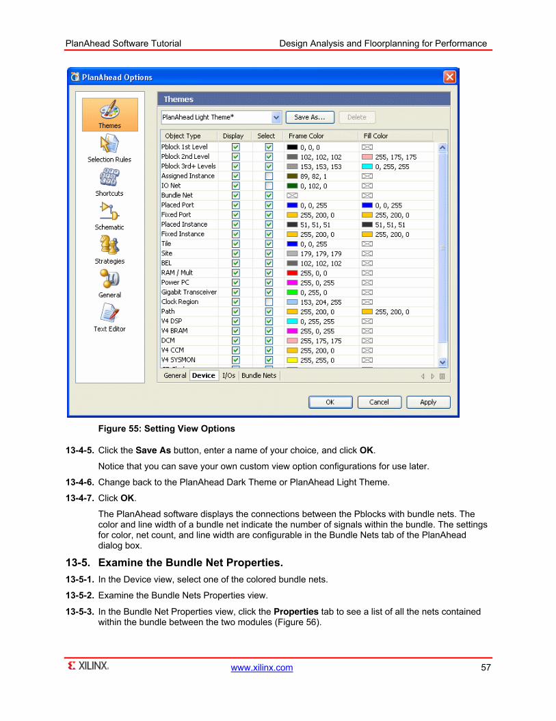
PlanAhead Software Tutorial Design Analysis and Floorplanning for Performance
www.xilinx.com 57
Figure 55: Setting View Options
13-4-5. Click the Save As button, enter a name of your choice, and click OK.
Notice that you can save your own custom view option configurations for use later.
13-4-6. Change back to the PlanAhead Dark Theme or PlanAhead Light Theme.
13-4-7. Click OK.
The PlanAhead software displays the connections between the Pblocks with bundle nets. The color and line width of a bundle net indicate the number of signals within the bundle. The settings for color, net count, and line width are configurable in the Bundle Nets tab of the PlanAhead dialog box.
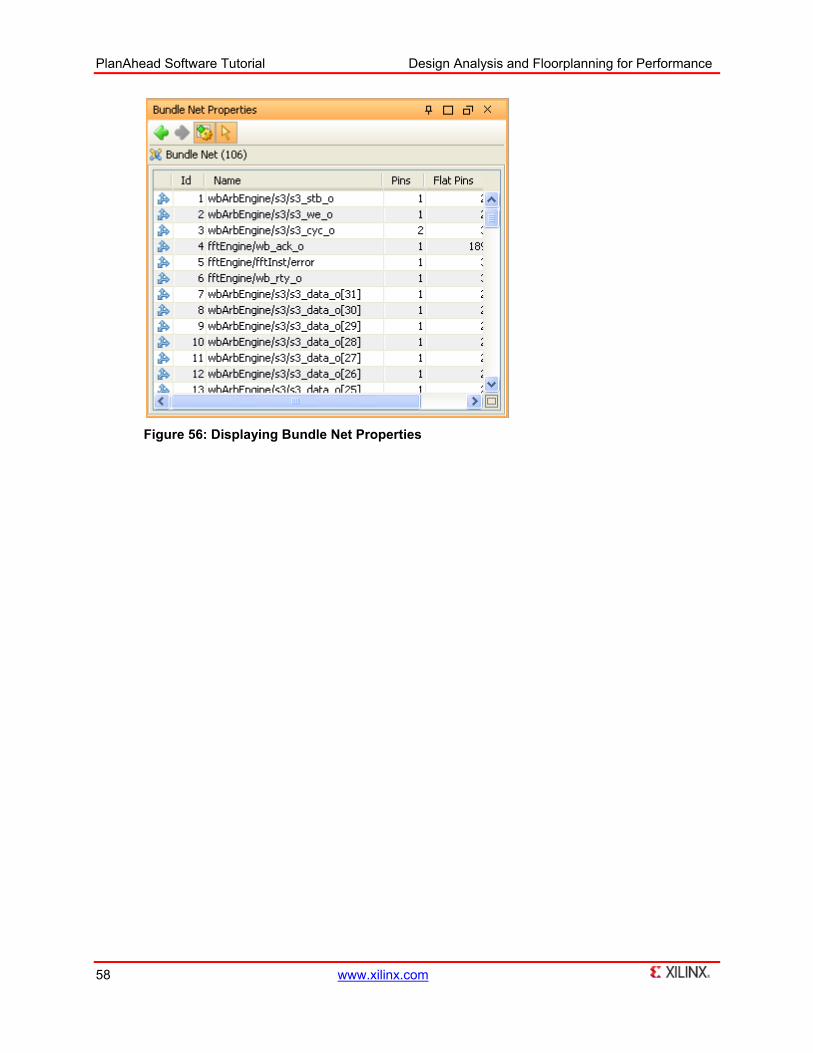
13-5. Examine the Bundle Net Properties. 13-5-1. In the Device view, select one of the colored bundle nets.
13-5-2. Examine the Bundle Nets Properties view.
13-5-3. In the Bundle Net Properties view, click the Properties tab to see a list of all the nets contained within the bundle between the two modules (Figure 56).
PlanAhead Software Tutorial Design Analysis and Floorplanning for Performance
58 www.xilinx.com
Figure 56: Displaying Bundle Net Properties

PlanAhead Software Tutorial Design Analysis and Floorplanning for Performance
www.xilinx.com 59
Step 14: Using the Search Capability to View Clock Domains Step 14
Effective floorplanning is often dependent on proper placement of the synchronous elements in different clock domains. You can highlight clock domains to visualize connectivity, enabling proper Pblock placement relative to clock regions.
14-1. Select and mark the global clock nets. 14-1-1. Select Edit > Find.
14-1-2. In the Find dialog box, set the following options:
• Find: Nets
• First field: Type
• Second field: is
• Third field: Global Clock
14-1-3. Ensure the Unique Nets Only button is enabled, and click OK.
14-1-4. Select the Pins column header twice to sort the Find Results view.
14-1-5. In the Find Results view list, select usbClk_BUFGP .
Notice the highlighted net leading to I/Os in the two usbEngine Pblocks (Figure 57).
Figure 57: Viewing Clock Net Destinations
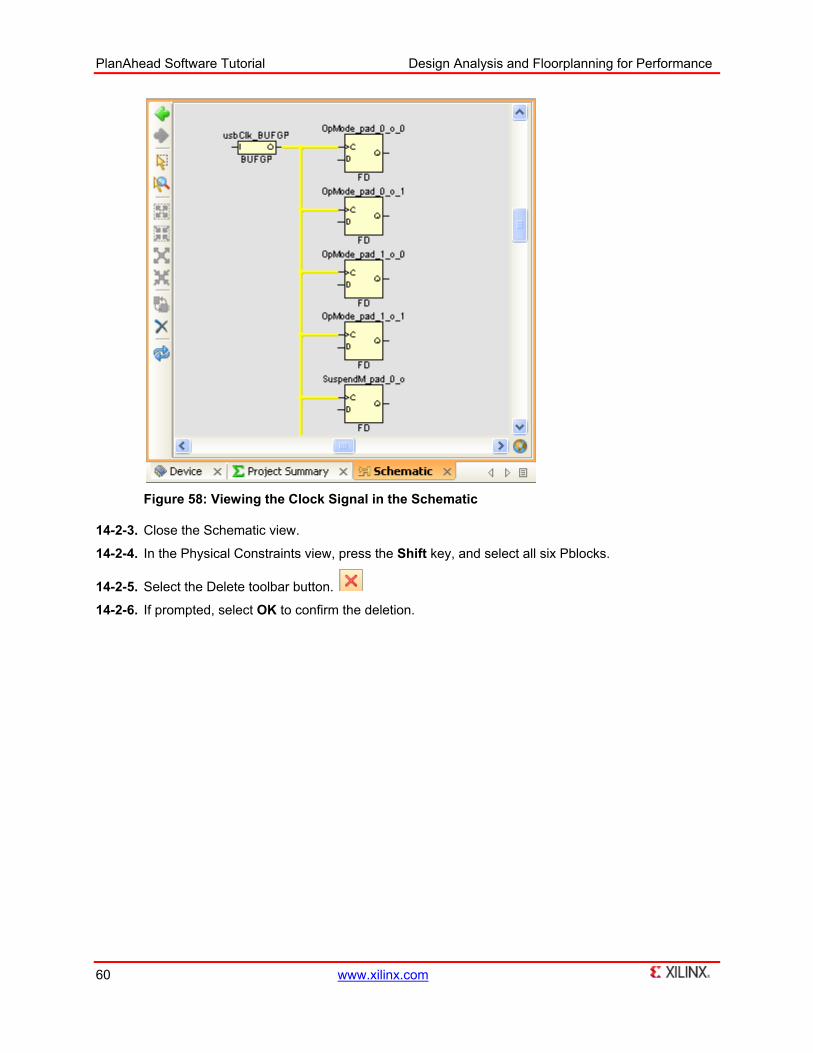
14-2. Use the Schematic View to see how the global clock net fans out to the primitives in the design.
14-2-1. With the global clock net still selected in the Find Results view, right-click and select the Schematic popup menu command.
The Schematic view shows the usbClk_BUFGP net connected to a group of registers.
14-2-2. At the top of the schematic, Zoom in on the usbClk_BUFGP BUFGP (Figure 58).
PlanAhead Software Tutorial Design Analysis and Floorplanning for Performance
60 www.xilinx.com
Figure 58: Viewing the Clock Signal in the Schematic
14-2-3. Close the Schematic view.
14-2-4. In the Physical Constraints view, press the Shift key, and select all six Pblocks.
14-2-5. Select the Delete toolbar button.
14-2-6. If prompted, select OK to confirm the deletion.

PlanAhead Software Tutorial Design Analysis and Floorplanning for Performance
www.xilinx.com 61
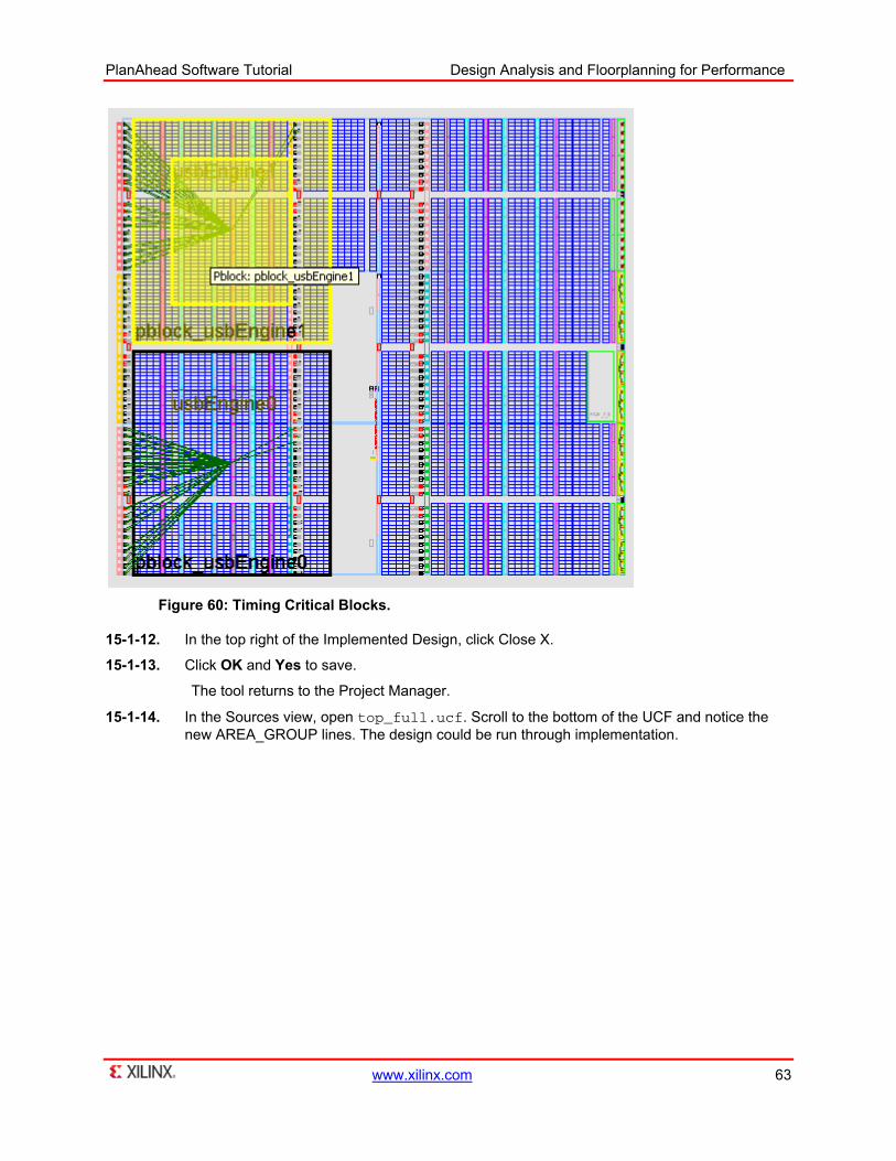
Step 15: Floorplanning Timing-Critical Hierarchy Step 15
Floorplanning a timing critical hierarchy can improve timing performance. The previous steps show that usbEngine1 and usbEngine0 contain timing critical logic. The usbEngine1 and usbEngine0 could go in the corners on the left-hand side. Many Pblocks were created to view the connectivity. Running all the Pblocks through implementation will hurt timing. Instead, floorplan just the timing critical hierarchies.
15-1. Place Pblocks for timing critical hierarchy. 15-1-1. Click the Device tab.
15-1-2. In the Device view, ensure that I/O Nets are being displayed .
15-1-3. In the Netlist view, select the Collapse All button .
15-1-4. In the Netlist view, select usbEngine0.
15-1-5. From the Device view toolbar, select Draw Pblock .
The cursor turns to a cross.
15-1-6. Draw a rectangle in the bottom left-corner of the device view.
15-1-7. Look at the Pblock Properties.
15-1-8. Click on the Statistics tab.
This Pblock is being sized to go through implementation.
15-1-9. Size the Pblock to have100% block RAM Utilization and approximately 60% Slices utilization. Do not span the center column gap. See Figure 59 for the Pblock placement.
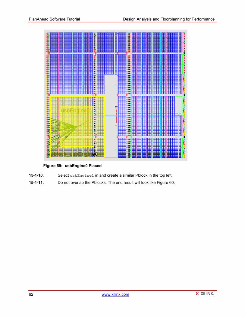
PlanAhead Software Tutorial Design Analysis and Floorplanning for Performance
62 www.xilinx.com
Figure 59: usbEngine0 Placed
15-1-10. Select usbEngine1 in and create a similar Pblock in the top left.
15-1-11. Do not overlap the Pblocks. The end result will look like Figure 60.
PlanAhead Software Tutorial Design Analysis and Floorplanning for Performance
www.xilinx.com 63
Figure 60: Timing Critical Blocks.
15-1-12. In the top right of the Implemented Design, click Close X.
15-1-13. Click OK and Yes to save.
The tool returns to the Project Manager.
15-1-14. In the Sources view, open top_full.ucf. Scroll to the bottom of the UCF and notice the new AREA_GROUP lines. The design could be run through implementation.

PlanAhead Software Tutorial Design Analysis and Floorplanning for Performance
64 www.xilinx.com
Conclusion In this tutorial, you used the PlanAhead software to explore and analyze the synthesized design and targeted device prior to running the implementation tools. This enabled you to find potential design issues and errors early in the design cycle, rather than discovering issues during implementation. In addition, you used the graphical presentation of design resource estimates, design rule violations, timing estimation, constraints and connectivity to help you understand your design and any potential problem areas.
After running the design through the implementation tools, you imported implementation results and examined timing results. You then analyzed critical path objects in the schematic and selected the parent modules of those path objects. You highlighted module placement and displayed the connectivity of the modules using the Show Connectivity command. You cleared the ISE software-assigned placement constraints. After analyzing the design, you created a floorplan to improve timing.