piezoresistive pressure sensors - uio.no · end force (e.g. protein attached) capacitive measure...
TRANSCRIPT

Piezoresistive pressure sensors
1Electronics and Cybernetics

Two sensing principlesPiezoresistivemeasure mechanical stress in doped resistor-areadiaphragm pressure sensorbending beam due to
volume forces (e.g. acceleration)end force (e.g. protein attached)
capacitivemeasure deflection (distance to other capacitor plate)diaphragm pressure sensorbending beam due to
volume forces (e.g. acceleration)end force (e.g. protein attached)
2Electronics and Cybernetics

Piezoresistive sensing applications
Load cell AccelerometerPressure sensor
3Electronics and Cybernetics
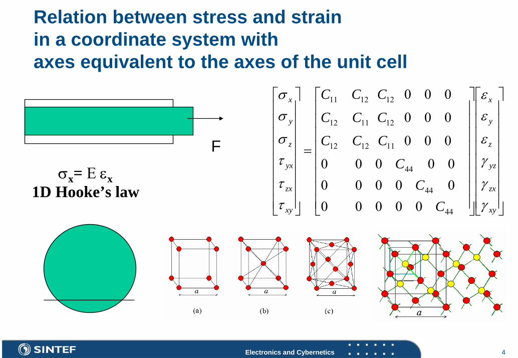
Relation between stress and strain in a coordinate system with axes equivalent to the axes of the unit cell
4Electronics and Cybernetics
⎥⎥⎥⎥⎥⎥⎥⎥
⎦
⎤
⎢⎢⎢⎢⎢⎢⎢⎢
⎣
⎡
⎥⎥⎥⎥⎥⎥⎥⎥
⎦
⎤
⎢⎢⎢⎢⎢⎢⎢⎢
⎣
⎡
=
⎥⎥⎥⎥⎥⎥⎥⎥
⎦
⎤
⎢⎢⎢⎢⎢⎢⎢⎢
⎣
⎡
xy
zx
yz
z
y
x
xy
zx
yx
z
y
x
CC
C
CCC
CCC
CCC
γγ
γε
εε
ττ
τσ
σσ
44
44
44
111212
121112
121211
000000000000000
000
000
000
F
σx= E εx1D Hooke’s law

Small deflectionsBeam equation, plate equation
Beam equation:
Plate equation:
Find displacement and stress
qdx
wdEI =4
4
F
),()2( 4
4
22
4
4
4
yxqyw
yxw
xwD =
∂∂
+∂∂
∂+
∂∂
p
5Electronics and Cybernetics
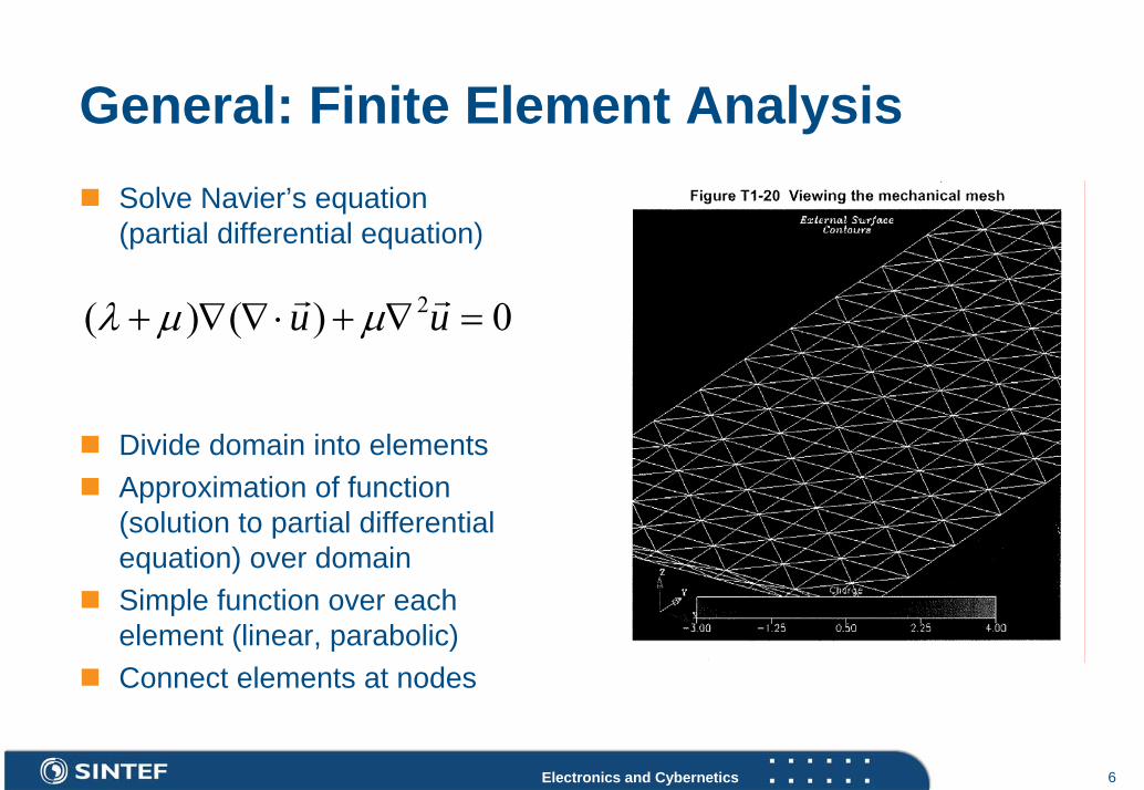
General: Finite Element Analysis
6Electronics and Cybernetics
Solve Navier’s equation (partial differential equation)
Divide domain into elementsApproximation of function (solution to partial differential equation) over domain Simple function over each element (linear, parabolic)
0)()( 2 =∇+⋅∇∇+ uu rr µµλ
Connect elements at nodes

7Electronics and Cybernetics
Example: beam with end load
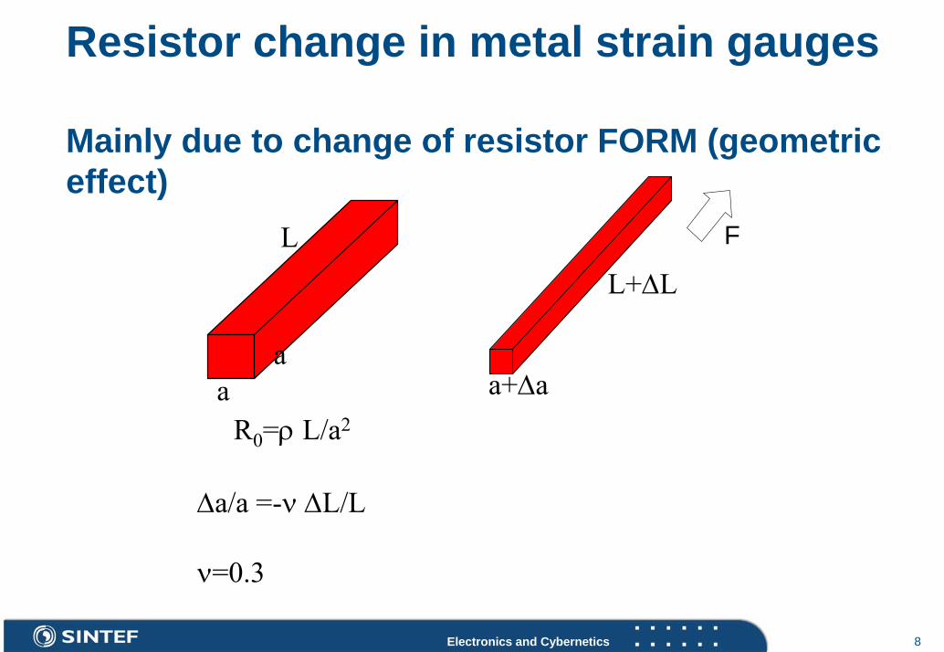
Resistor change in metal strain gauges
Mainly due to change of resistor FORM (geometric effect)
8Electronics and Cybernetics
F
a+∆a
L+∆L
aa
L
R0=ρ L/a2
∆a/a =-ν ∆L/L
ν=0.3

For silicon: large RESISTIVITY change with stress(not mainly a geometric resistor-change factor)
+ -+ -+ -+ -+ -+ -+ -+ -+ -+ -+ -+ -+ -+ -+ -+ -+ -+ -+ -+ -+ -+ -+ -+ - + -+ -+ -+ -+ -+ -+ -+ -+ -+ -+ -+ -+ -+ -+ -+ -+ -+ -+ -+ -+ -+ -+ -+ - + -+ -+ -+ -+ -+ -+ -+ -+ -+ -+ -+ -+ -+ -+ -+ -+ -+ -+ -+ -+ -+ -+ -+ - + -+ -+ -+ -+ -+ -+ -+ -+ -+ -+ -+ -+ -+ -+ -+ -+ -+ -+ -+ -+ -+ -+ -+ - + -+ -+ -+ -+ -+ -+ -+ -+ -+ -+ -+ -+ -+ -+ -+ -+ -+ -+ -+ -+ -+ -+ -+ -
+ -+ -+ -+ -+ -+ -+ -+ -+ -+ -+ -+ -+ -+ -+ -+ -+ -+ -+ -+ -+ -+ -+ -+ - + -+ -+ -+ -+ -+ -+ -+ -+ -+ -+ -+ -+ -+ -+ -+ -+ -+ -+ -+ -+ -+ -+ -+ - + -+ -+ -+ -+ -+ -+ -+ -+ -+ -+ -+ -+ -+ -+ -+ -+ -+ -+ -+ -+ -+ -+ -+ - + -+ -+ -+ -+ -+ -+ -+ -+ -+ -+ -+ -+ -+ -+ -+ -+ -+ -+ -+ -+ -+ -+ -+ - + -+ -+ -+ -+ -+ -+ -+ -+ -+ -+ -+ -+ -+ -+ -+ -+ -+ -+ -+ -+ -+ -+ -+ -
+ -+ -+ -+ -+ -+ -+ -+ -+ -+ -+ -+ -+ -+ -+ -+ -+ -+ -+ -+ -+ -+ -+ -+ - + -+ -+ -+ -+ -+ -+ -+ -+ -+ -+ -+ -+ -+ -+ -+ -+ -+ -+ -+ -+ -+ -+ -+ - + -+ -+ -+ -+ -+ -+ -+ -+ -+ -+ -+ -+ -+ -+ -+ -+ -+ -+ -+ -+ -+ -+ -+ - + -+ -+ -+ -+ -+ -+ -+ -+ -+ -+ -+ -+ -+ -+ -+ -+ -+ -+ -+ -+ -+ -+ -+ - + -+ -+ -+ -+ -+ -+ -+ -+ -+ -+ -+ -+ -+ -+ -+ -+ -+ -+ -+ -+ -+ -+ -+ -
+ -+ -+ -+ -+ -+ -+ -+ -+ -+ -+ -+ -+ -+ -+ -+ -+ -+ -+ -+ -+ -+ -+ -+ - + -+ -+ -+ -+ -+ -+ -+ -+ -+ -+ -+ -+ -+ -+ -+ -+ -+ -+ -+ -+ -+ -+ -+ - + -+ -+ -+ -+ -+ -+ -+ -+ -+ -+ -+ -+ -+ -+ -+ -+ -+ -+ -+ -+ -+ -+ -+ - + -+ -+ -+ -+ -+ -+ -+ -+ -+ -+ -+ -+ -+ -+ -+ -+ -+ -+ -+ -+ -+ -+ -+ - + -+ -+ -+ -+ -+ -+ -+ -+ -+ -+ -+ -+ -+ -+ -+ -+ -+ -+ -+ -+ -+ -+ -+ -
+ -
+ -
+ -
+ -
+ -
+ -
+ -
+ -
+ -
+ -
+ -
+ -
+ -
+ -
+ -
+ -
+ -
+ -
+ -
+ -
∆R/R ≈ 2 ε
Metal:
+ +- -
∆R/R ≈ 90 ε
Silicon:
9Electronics and Cybernetics

Electronics (Chapter 14.1 - 14.4) Doped resistors
10Electronics and Cybernetics
Define a p-type circuitin a n-type wafer
n-type wafer must be at positivepotential relative to the p-type circuit
Reverse biased diode → no current between circuit and wafer/substrate
+V-
n p
Alternative methods:•SOI•Surface micromachining

The resistivity changes with the mechanical stress
11Electronics and Cybernetics
E - electric field, three componentsj - current density, three componentsρ0 – homogeneous resistivity, unstressed silicon
When mechanical stress is applied, the resistivity changes depending on the stress in different directions and the piezocoefficients
⎥⎥⎥
⎦
⎤
⎢⎢⎢
⎣
⎡
⎥⎥⎥
⎦
⎤
⎢⎢⎢
⎣
⎡+
⎥⎥⎥
⎦
⎤
⎢⎢⎢
⎣
⎡=
⎥⎥⎥
⎦
⎤
⎢⎢⎢
⎣
⎡
3
2
1
345
426
561
0
3
2
1
0
3
2
1
jjj
ddddddddd
jjj
EEE
ρρ
V1 V2

Silicon: Three independent piezoresistive coefficients
⎥⎥⎥
⎦
⎤
⎢⎢⎢
⎣
⎡
⎥⎥⎥
⎦
⎤
⎢⎢⎢
⎣
⎡+
⎥⎥⎥
⎦
⎤
⎢⎢⎢
⎣
⎡=
⎥⎥⎥
⎦
⎤
⎢⎢⎢
⎣
⎡
3
2
1
345
426
561
0
3
2
1
0
3
2
1
jjj
ddddddddd
jjj
EEE
ρρExample of piezoresistive coefficients:
doping: p-typesheet resistivity: 7.8 Ωcm
value of Π11= 6.6 10-11 Pa-1
value of Π12=-1.1 10-11 Pa-1
value of Π44= 138 10-11 Pa-1
Equations 18.3, 18.4, 18.5 in Senturia
12Electronics and Cybernetics
⎥⎥⎥⎥⎥⎥⎥⎥
⎦
⎤
⎢⎢⎢⎢⎢⎢⎢⎢
⎣
⎡
⎥⎥⎥⎥⎥⎥⎥⎥
⎦
⎤
⎢⎢⎢⎢⎢⎢⎢⎢
⎣
⎡
ΠΠ
Π
ΠΠΠ
ΠΠΠ
ΠΠΠ
=
⎥⎥⎥⎥⎥⎥⎥⎥
⎦
⎤
⎢⎢⎢⎢⎢⎢⎢⎢
⎣
⎡
xy
zx
yx
z
y
x
dddddd
ττ
τσ
σσ
44
44
44
111212
121112
121211
6
5
4
3
2
1
000000000000000
000
000
000
13Electronics and Cybernetics
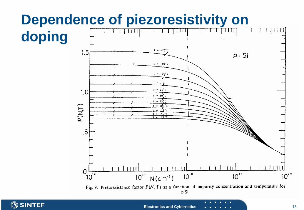
Dependence of piezoresistivity on doping
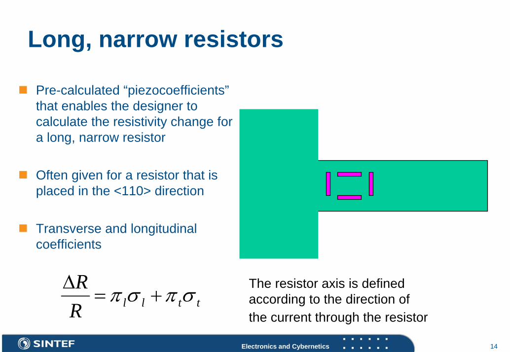
Long, narrow resistors
Pre-calculated “piezocoefficients”that enables the designer to calculate the resistivity change for a long, narrow resistor
Often given for a resistor that is placed in the <110> direction
Transverse and longitudinal coefficients
14Electronics and Cybernetics
ttllRR σπσπ +=
∆ The resistor axis is definedaccording to the direction ofthe current through the resistor

Resistors along <110> direction in (100) wafers
15Electronics and Cybernetics
Much used direction for piezoresistors, bulk micromachiningPre-calculated longitudinal and transverse piezo-coefficients
σ positive: tensile stressσ negative: compressible stressπ positive: increased resistivity with tensile stressπ negative: decreased resistivitywith tensile stress
p-type silicon: π44 dominates
)(2
)(2/1
)(2/1
44
441211
441211
tl
t
l
RR σσπ
ππππ
ππππ
−≈∆
−+=
++=

Beam accelerometer
Long resistors in <110> direction
Piezoresistive coefficients
16Electronics and Cybernetics
n-type: πl = -31.2 πt = -17.6
p-type: πl = 71.8 πt = -66.3

Cantilever with piezoresistors
17Electronics and Cybernetics
length 200 µmwidth 20 µmthickness 5 µm
point load at free end1 µm deflection
p-type piezoresistorlength 20 µmwidth 2 µmdepth 0.2 µm
∆R/R = πl σl =0.02

Placement of piezoresistors on diaphragm
Over/under konfigurasjoner ikke praktisk i silisium.
Men vi kan snu retningenpå motstandene
18Electronics and Cybernetics

Piezoresistor placed normal to diaphragm edge
19Electronics and Cybernetics
Apply pressure from aboveDiaphragm bends downPiezoresistor is stretched longitudinallyσl is positive, tensile stressRough argument for mechanical stress in transversal direction: stress must avoid contraction: σt= σlνTransverse stress is tensile/positiveChange in resistance:
(πt is negative)Resistance increases
ltlRR σνππ )(/ 11 +=∆ttllR
R σπσπ +=∆
p-type piezoresistor along<100> direction in (100) wafer

20Electronics and Cybernetics
Piezoresistor placed parallel to diaphragm edgeApply pressure from aboveDiaphragm bends downPiezoresistor is stretched transversallyσt is positiveRough argument for mechanical stress in longitudinal direction: stress must avoid contraction: σl= σtνTensile, positive stress in longitudinal dir.Change in resistance:
(πt is negative)Resistance decreases
tltRR σνππ )(/ 22 +=∆p-type piezoresistor along<100> direction in (100) wafer

Membrane pressure sensor
21Electronics and Cybernetics

Wheatstone bridge circuit
22Electronics and Cybernetics
<100> direction
⎟⎠⎞
⎜⎝⎛∆=
∆+=∆−=∆+=∆−=
⎟⎟⎠
⎞⎜⎜⎝
⎛+
−+
=
RRVV
RRRRRRRRRRRR
RRR
RRRVV
s
s
0
44
33
22
11
43
3
12
20
3.668.71
−==
t
l
ππ
stress lecompressib negative, stress tensilepositive,
σσ

Pressure Measurement in MedicineExample: Hydrocephalus
23Electronics and Cybernetics
abnormal accumulation of brain fluidincreased brain pressureoccurs in approximately one out of 500 birthstreated by implantation of a shunt system

Complex requirements for the measurement system
24Electronics and Cybernetics
Small dimensionsEffective pressure transmissionNo wires through the skin No batteriesMaterial acceptable for MRI scans

The sensor
PiezoresistiveSurface micro machined Wheatstone bridge
two piezoresistors on diaphragmtwo on substrate for temperature reasons
Absolute pressure sensor
25Electronics and Cybernetics

Sensor design
26Electronics and Cybernetics

Sensor design
Si3N4SiO2polySi
(Al)
(polySi)
27Electronics and Cybernetics
(not to scale)
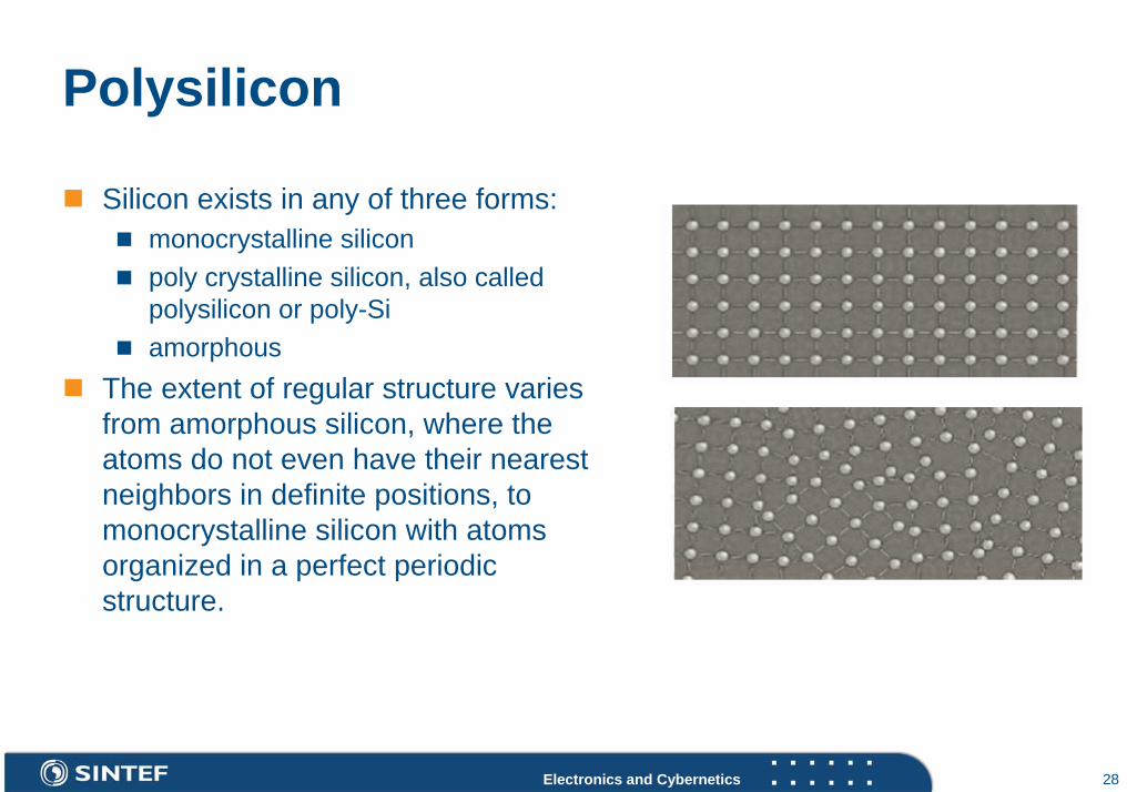
Polysilicon
28Electronics and Cybernetics
Silicon exists in any of three forms: monocrystalline siliconpoly crystalline silicon, also called polysilicon or poly-Siamorphous
The extent of regular structure varies from amorphous silicon, where the atoms do not even have their nearest neighbors in definite positions, to monocrystalline silicon with atoms organized in a perfect periodic structure.

Transmission electron microscope (TEM) picture of a Metal-Oxide Semiconductor Field-Effect Transistor (MOSET) gate consisting of a 2 nm thick amorphous silicon oxide layer between crystalline silicon (top) and polycrystalline silicon (bottom). Image by Reed electronics group/FEI Company.
29Electronics and Cybernetics

Piezoresistivity in polysilicon
30Electronics and Cybernetics
The piezoresistive coefficients loose sensitivity to crystalline directionAverage over all orientationsGauge factor of 20 – 40, about one fifth of the gauge factor of monocrystalline siliconGauge factor up to 70% of monosilicon has been reportedThe structure; i.e. the grain size and the texture (preferred orientation of the crystallites) is decisive for the piezoresistivityThe longitudinal gauge factor is always larger than the transverse one

Functionality & sensitivity
31Electronics and Cybernetics

32Electronics and Cybernetics
Microcantilevers with piezoresistiv sensing; applications in biochemical and chemical sensors

Application Areas
Photo: SINTEF/Stanford
33Electronics and Cybernetics
Life sciences researchMedical diagnostics and analysisDrug discoveryDrug deliveryEnvironmental monitoring Process control e.g. oil industry and food industryFood analysisSecurity devices e.g. detection of explosives Energy technology including fuel cells

Beam BendingBeam bendingThe difference in surface tension (upper side/lower side) and the radius of curvature are related through
For a cantilever ^
Stoney’s formula
Typical beam dimensions: 150 x 50 x 0,5 µmBeams often made of Si, SiNx or a polymer width a thin functional layer on top of one of the beam surfaces, typical 30 nm
EIM
R=
1 3
121 bhI =
σν∆
−= 2
2 )1(3Eh
Ls
Ref: C. Ziegler, anal. Bioanal Chem 379 (2004)
)(1612 σν
∆⎟⎠⎞
⎜⎝⎛ −
=EhR
34Electronics and Cybernetics

Add-on processes – bioactive layers
35Electronics and Cybernetics
Functional surfaces for attachment of:proteins (antibodies)single strandedoligo-nucleotidesglucose molecules…
Au or NiCr/Au films on siliconCommercial or customers’ own biochemistryTo be combined with lab-on-chip systems
K.W. Wee et al. 2005

Påvisning av biokjemisk eller kjemisk effekt
36Electronics and Cybernetics
Optisk vektstangsprinsippInterferometriOptiske filtreKapasitivPiezoresistiv
Bilde fra Protiveris, figur fra L. G Carrascosa et a. Trends in Analytical Chemistry, 25 (2006)

Piezoresistiv utlesning
37Electronics and Cybernetics
+ Store og kostbare optiske komponenter samt tidkrevende laseroppstilling er unødvendig
+ Fungerer i både gass (luft) og væsker, også i ugjennomsiktige væsker+ Utlesningselektronikk og temperaturkontroll kan integreres på samme chip
som bjelken(e)+ Temperaturen på bjelkene kan endres ved å endre strømmen gjennom
motstandene, gjenbruk ved å bryte molekylbindinger?- Innebygget støy som påvirker oppløsing og følsomhet- Krever elektrisk tilkopling

DNA-analyse
38Electronics and Cybernetics
Bjelkens overflate belagt med AuDifferensiell målingTo nukleotidkjeder bestående av 12 baser, hvor to av basene er ulike:
CTATGTCAGCACCTATGTAAGCAC
Nedbøyning 1: 10 nm , Nedbøyning 2: 0 nmForskjeller i ett basepar kan detekteres! nukleotid
Ref.: J. Fritz et al. Science 288 (2000)

Elektronisk nese
39Electronics and Cybernetics
Hver bjelke er belagt med ulike polymerer (~ 5µm) på gull (30 nm)Polymerlagene sveller under kontakt med gasskomponenterSvelle- eller fordampnings-prosessens forløp er avhengig av damptrykk og løselighet i den enkelte polymer og gir et ”fingeravtrykk”Informasjonen analyseres av et mønstergjenkjenningssystemFølsomhet for 1-propanol: ca.30 ppm/µm nedbøyning
Ref.: M. K Baller et al. Ultramicroscopy 82 (2000)