piezoelectric actuators with integrated high voltage power
TRANSCRIPT

1
Piezoelectric Actuators with Integrated HighVoltage Power Electronics
Y. K. Yong, Member, IEEE, A. J. Fleming, Member, IEEE
Abstract—This article explores the possibility of piezoelectricactuators with integrated high voltage power electronics. Suchdevices dramatically simplify the application of piezoelectricactuators since the power electronics are already optimized forthe voltage range, capacitance, and power dissipation of theactuator. The foremost consideration is the thermal impedance ofthe actuator and heat dissipation. Analytical and finite-elementmethods are described for predicting the thermal impedanceof a piezoelectric bender. The predictions are compared experi-mentally using thermal imaging on a piezoelectric bender withlaminated miniature power electronics.
Index Terms—Piezoelectric, Actuators, Power Electronics
I. INTRODUCTION
Piezoelectric transducers have become ubiquitous in ap-plications requiring precision motion and force control. Forexample, positioning systems [1]–[4], micro-motors [5]–[8],machine tools [9], pumps [10], surgical tools [11], fuel injec-tors [12], scanning probe microscopes (SPMs) [13]–[16], andvibration control systems [17], [18].
In addition to the high resolution [19], piezoelectric actu-ators are also desirable for their low mass, dimensions, andzero static power consumption. However, these benefits maybe negated by the requirement for an external high-voltageamplifier, power supply, sensors, and a feedback loop. In someapplications, feed-forward control can alleviate the need forsensors and a feedback loop [20]–[22], however the drivingelectronics are still required.
The requirement for an external high voltage amplifier hassignificantly limited the feasibility of miniaturized piezoelec-tric systems. For example, a piezoelectric microgripper stillrequires bulky support electronics (100mm×100mm) eventhough the device itself is only 23 mm in width [23]. Thisalso necessitates the need for high-voltage wiring betweenthe driver and actuator. Piezoelectric bender actuators havealso shown promise in micro-robotic applications. In reference[24], an energy recovery circuit was designed to reduce thesize of the drive electronics so that they could be mountedon-board the robot. Bimorph actuators have also been usedfor piezoelectric motors with nanometer resolution [25].
In sensing applications, the conditioning electronics areroutinely integrated with the transducer to avoid interferencefrom high-impedance wiring. For example, accelerometers areproduced with an integrated FET amplifier [26]. However, itis not trivial to apply such techniques for actuation since the
The authors are with the School of Electrical Engineering and ComputerScience, The University of Newcastle, Callaghan 2308, NSW, Australia.Email: [email protected], [email protected]
drive electronics are significantly more complicated, requireinductive components, and may also dissipate heat.
This work investigates the feasibility of a piezoelectricbimorph actuator with integrated power electronics. Due to therecent availability of high-voltage integrated circuits, it is nowfeasible to construct a complete high-voltage power supplyand amplifier in an area smaller than 7 mm2. The driver canthen be thermally attached to the actuator for heat dissipation.This technique is demonstrated in Section II.
The required power dissipation is derived in Section IIIwhich defines the required thermal impedance of the actuatorfrom the mounting location to the ambient environment. Ana-lytical and finite-element techniques are applied to estimate thethermal impedance of the actuator in Section IV. The actuatoris found to be capable of easily dissipating the required powerwith negligible erroneous deflection due to thermal expansion.The predictions are compared to experimental results in Sec-tion V.
By integrating the power electronics and actuator, the elec-trical design process is effectively eliminated. This dramati-cally reduces the cost and complexity of installing piezoelec-tric actuators in industrial and automotive applications wherethere may be a restriction on the maximum wiring voltage.This level of miniaturization also creates new possibilitiesfor autonomous piezoelectric walking and flying robots withindependent control over each actuator. For example, a six-legged robot could be designed with independent control overeach limb from a single 3.7 V battery cell.
II. EXAMPLE BIMORPH ACTUATOR WITH INTEGRATEDDRIVER
A. Actuator
The actuator is a two-layer brass reinforced bimorph ben-der from Piezosystems Inc. (Q220-A4-503YB). Both of thepiezoelectric layers are poled in the same direction and drivenelectrically in parallel, i.e. the top and bottom surfaces aregrounded and the internal layer is driven. The bender is fixedonto a mounting base as shown in Fig. 1. The propertiesof interest are listed in Table I. The static and dynamicbehavior of piezoelectric bimorphs is described, for example,in reference [27].
B. Power Electronics
The power electronic module is a PiezoDrive PDu100 driver[28] illustrated in Fig. 2. The power supply is a closed-loopboost converter that produces 105 V from a 3 V to 5.5 Vsupply. The supply voltage is compatible with a single Lithium

2
Bimorph
Power Electronics
Sensor
Base
Fig. 1. Piezoelectric bimorph actuator with thermally attached power elec-tronics.
TABLE IPROPERTIES OF THE PIEZO SYSTEMS Q220-A4-503YB BENDER
ACTUATOR.
Dimensions 63.5 x 31.8 x 0.51 mmPiezo Material 5A4E
Curie Temperature 350 ◦CVoltage ±90 V
Mounted Deflection ±1.26 mmMounted Stiffness 245 N/m
Mounted Blocking Force 0.31 NMounted Resonance Freq. 68 Hz
Capacitance 260 nF
Ion or Polymer battery cell. To obtain a bipolar output voltage,the load is driven by two linear amplifiers with opposite gain,effectively doubling the output voltage range to ±100 V.
The circuit and support electronics are mounted on a ther-mally conductive PCB with an area of 12 mm2. Approximatelyhalf the area is used for connecting pads so the size could bereduced to less than 7 mm2 if necessary. These dimensionsare compatible with many of bender geometries.
The module is bonded to the actuator using an adhesivethermally conductive insulator (T-Global LI-98-150-025). Thismaterial is a soft elastomer which effectively decouples thestrain of the actuator from the high-stiffness of the PCB. Threelayers of 0.25 mm thickness were used for a total thicknessof 0.75 mm.
The connection diagram for the electronics and actuator isshown in Fig. 3. An input signal of ±1.65 V with an offset of2.5 V produces a ±90 V output signal which is the full rangeof the actuator.
C. Sensor Design
The position is measured with an OPB703 reflective sen-sor and the conditioning circuit illustrated in Fig. 4. Whendriven with a 40 mA current, the phototransistor current isproportional to the distance over a range of approximately 2.5
Operation The system block diagram is illustrated in Figure 2. A boost converter generates a high-voltage rail to supply a pair of complementary amplifiers. A single output can be used to drive a unipolar load up to V or both amplifiers can be used to produce V. The input is selectable between a unipolar signal biased at half the supply voltage or a bipolar signal. The amplifier gain is 27.5 so a 3.6 Vp-p input will produce a 100 Vp-p output. Both amplifier channels are biased at half the output range (50 V).
The overall system gain is determined by the output configuration. The possible combinations are listed below.
Output Type
Gain Input Range
Output Range
Unipolar 27.5 ½ Vs V 100 V
Bipolar 55 ½ Vs V V
Table 1. System gain and voltage range
Both output amplifiers are biased at approximately half the HV Bus voltage, i.e. 50 V. The gain and output voltage ranges can be customized by contacting [email protected].
Output Current The maximum average output current is 15 mA. However, for periods less than 100 us an output current of approximately 100 mA is possible. This is useful for achieving small, high-speed step changes in the output voltage.
Example Applications Some typical application circuits are shown below. The optional output resistance Ro is used to reduce noise as described in “Noise” on page 3.
Power Bandwidth The output slew-rate of the PDu100 is 1 V/us. Therefore, the maximum frequency sine-wave is
Boost Converter
Supply 3V - 5.5V Bias
Voltage
HV Bus
Bias Voltage
27.5
-27.5
Input Offset
Vs 1.8V
Bipolar Load
+ +
Unipolar Load +
-
Enable
Figure 2. PDu100B Block Diagram
Figure 3. Application circuits
100 V Three-wire bender driver with bias
0V to 60V
0V to 100V
100 V Piezo stack driver with 50 V bias
90 V
90 V Piezo bender driver
+ -
g
Vb Vs
g
Vin en
+
Ro
5V
Input V 1.8V
+ -
g
Vb Vs
g
Vin en
5V
Input V 1.65V +
Ro
+ -
g
Vb Vs
g
Vin en
5V
Input V 1.8V
+
+
Ro
100V
0V to 100V
Ro 100V to 0V
+ -
g
Vb Vs
g
Vin en
5V
Input V 1.1V
60 V Push-pull stack driver or bender driver
+ +
Ro
Ro
Fig. 2. Power electronics functionality [28].
Operation The system block diagram is illustrated in Figure 2. A boost converter generates a high-voltage rail to supply a pair of complementary amplifiers. A single output can be used to drive a unipolar load up to V or both amplifiers can be used to produce V. The input is selectable between a unipolar signal biased at half the supply voltage or a bipolar signal. The amplifier gain is 27.5 so a 3.6 Vp-p input will produce a 100 Vp-p output. Both amplifier channels are biased at half the output range (50 V).
The overall system gain is determined by the output configuration. The possible combinations are listed below.
Output Type
Gain Input Range
Output Range
Unipolar 27.5 ½ Vs V 100 V
Bipolar 55 ½ Vs V V
Table 1. System gain and voltage range
Both output amplifiers are biased at approximately half the HV Bus voltage, i.e. 50 V. The gain and output voltage ranges can be customized by contacting [email protected].
Output Current The maximum average output current is 15 mA. However, for periods less than 100 us an output current of approximately 100 mA is possible. This is useful for achieving small, high-speed step changes in the output voltage.
Example Applications Some typical application circuits are shown below. The optional output resistance Ro is used to reduce noise as described in “Noise” on page 3.
Power Bandwidth The output slew-rate of the PDu100 is 1 V/us. Therefore, the maximum frequency sine-wave is
Boost Converter
Supply 3V - 5.5V Bias
Voltage
HV Bus
Bias Voltage
27.5
-27.5
Input Offset
Vs 1.8V
Bipolar Load
+ +
Unipolar Load +
-
Enable
Figure 2. PDu100B Block Diagram
Figure 3. Application circuits
100 V Three-wire bender driver with bias
0V to 60V
0V to 100V
100 V Piezo stack driver with 50 V bias
90 V
90 V Piezo bender driver
+ -
g
Vb Vs
g
Vin en
+
Ro
5V
Input V 1.8V
+ -
g
Vb Vs
g
Vin en
5V
Input V 1.65V +
Ro
+ -
g
Vb Vs
g
Vin en
5V
Input V 1.8V
+
+
Ro
100V
0V to 100V
Ro 100V to 0V
+ -
g
Vb Vs
g
Vin en
5V
Input V 1.1V
60 V Push-pull stack driver or bender driver
+ +
Ro
Ro
Fig. 3. Connection diagram of the power electronics and actuator.
mm (centered at 2.5 mm). The op-amp acts as a photocurrentamplifier with a variable gain up to 10 V/mA. The zeropotentiometer is adjusted so that the output is zero voltswith zero deflection. Other possible sensor configurations arediscussed in [29].
III. ELECTRICAL CONSIDERATIONS
For the purposes of estimating electronic power dissipationat frequencies below the first resonance, a piezoelectric ac-tuator can be adequately modeled as a capacitor as shown inFig. 5(a) [30]. It should be noted that soft piezoceramics, suchas PZT-5H, exhibit significant hysteresis that can effectivelydouble the small-signal capacitance when driven at full range.
The power dissipation of the grounded amplifier in Fig. 5(a)can be found by summing the power supplied by the positiveand negative supplies,
Pd = V +I+av + V −I−av. (1)
For a capacitive load I+av = −I−av , therefore
Pd = (V + − V −)Iav. (2)
With a sinusoidal excitation, the peak load current is
IL(pk) = πVL(p−p)fCp. (3)

3
+12V
-12V
zero
10k
40mA
Gain
10k
Out
Fig. 4. Displacement sensor schematic diagram.
Vin
Cp
I
VL
V +
V -
Vin
Cp
I
VL
V +
V -
V +
V -
(a) Grounded load (a) Equivalent bridged configuration
L
L
12
1212
12
k
k
k2
-k2
Fig. 5. Electrical model of a piezoelectric actuator driven in the groundedconfiguration (a), and the equivalent bridged configuration (b).
The average current is therefore
Iav =1
2π
∫ π
0
IL(pk)sin(θ) dθ =IL(pk)
π. (4)
Thus, the power dissipation is
Pd = (V + − V −)VL(p−p)Cpf. (5)
The driver described in Section II-B operates in the bridgedconfiguration as shown in Fig. 5(b). To achieve the sameload voltage as the grounded circuit, the bridged configurationrequires only half the supply voltage. However, since theaverage load current is identical and there are two amplifiers,the total power dissipation of the bridged configuration isidentical to the grounded circuit.
In addition to the power dissipated by the amplifiers, thefinite efficiency of the boost converter must also be considered.If the converter efficiency is η, the total power dissipationbecomes
Pd =1
η(V + − V −)VL(p−p)Cpf. (6)
The above equation is relevant to any linear amplifier witha switched mode power supply operating in the standardor bridged configuration. It should be noted that η is thefull-load converter efficiency. The actual efficiency may varyunder lighter load conditions; however, this approximation issufficient for estimating the worst case power dissipation. For
QPiezo
Brasst
1
t2
Lw
x
TT
a
Fig. 6. A cantilever beam model with the fixed-end heated.
the bridged driver described in Section II-B, V +/2 = 105 V,V − = 0 V, and the efficiency is approximately η = 0.75.Therefore, the power dissipation is
Pd =210 V × 520 nF
0.75VL(p−p)f. (7)
With the full-scale ±90 V load voltage, the power dissipationis 26 mW/Hz. Thus, if the actuator is operated at the maximumoperating frequency of 60 Hz, the maximum power dissipationis approximately 1.5 W.
IV. THERMAL DISSIPATION
As discussed above, the power electronic module maydissipate up to 1.5 W. The thermal impedance of the mountinglocation must be low enough to ensure that the junction tem-perature of the electronics does not exceed 150◦C. Althoughthe Curie temperature of the piezoelectric material is 350◦C,the maximum practical temperature is also limited to around150◦C by the glue layers. To investigate the thermal dissipationof the bender, the thermal impedance is calculated analyticallyin this section. This result is compared to an ANSYS finite-element (FE) simulation and experimental results. The ther-mally induced deflection and extension of the bender is alsostudied by finite-element analysis.
A. Analytical Estimation
To estimate the thermal impedance, the temperature distri-bution of the bender is first calculated. The bimorph bender isthermally modeled as a fin. The Biot number (Bi = hct/2ka)of the bender is estimated to be < 0.1, where hc is the naturalconvection coefficient, t is the thickness and ka is the averagethermal conductivity of the bender. Bi < 0.1 shows that thebender has a uniform temperature along its thickness directionwhere temperature at the center will not differ from that ofthe surface by more than 5% [31]. Therefore, the temperaturedistribution along the thickness direction can be ignored,and only the temperature distribution along the longitudinaldimension is considered. As a result, the bender is modeledas one-dimensional fin.
As shown in Fig. 6, the bimorph is a cantilever beam withthe fixed-end heated by the integrated power electronics. Themaximum power is assumed to be Q = 1.65 W. Ta is theambient temperature, L is the length, w is the width and x isthe distance along the length of the bender. The temperature

4
TABLE IIDIMENSIONS AND PROPERTIES OF THE BENDER.
L w t1 t2 k1 k2mm mm mm mm W/mK W/mK63.5 31.8 0.2 0.1016 1.25 115
distribution profile of the bender along the x direction can befound by solving the following differential equation [31], [32],
d2T
dx− β2 [T (x)− Ta] = 0, (8)
where β2 = 2hc/ (2k1t1 + k2t2), k1 and t1 are the thermalconductivity and thickness of the piezoelectric layer respec-tively, k2 and t2 are the thermal conductivity and thickness ofthe brass layer respectively. Since β is a constant, Eq. (8) hasthe solution
T (x)− Ta = C1e−βx + C2e
βx. (9)
Assuming the thermal heating occurs at x = 0, we have aboundary condition
− (2k1A1 + k2A2)dT (0)
dx= Q,
−w (2k1t1 + k2t2)dT (0)
dx= Q,
dT (0)
dx=
−Qw (2k1t1 + k2t2)
. (10)
where A1 and A2 are the cross-sectional area of the piezo-electric and brass layer respectively. Differentiating Eq. (9),and equate it to Eq. (10), we have
C2 = C1 −Q
βw (2k1t1 + k2t2). (11)
Substituting Eq. (11) into Eq. (9), and by assuming that atx = L, T (L) = Ta, we have
C1 =Qe2βL
βw (2k1t1 + k2t2) (1 + e2βL). (12)
Substituting Eq. (12) into Eq. (11), we have
C2 =−Q
βw (2k2t1 + k2t2) (1 + e2βL). (13)
Eqs. (12) and (13) can be simplified to
C1 =QeβL
2βw (2k1t1 + k2t2) cosh (βL), (14)
C2 =−Qe−βL
2βw (2k1t1 + k2t2) cosh (βL). (15)
Substituting Eqs. (14) and (15) into (9), the temperature dis-tribution along the length direction of the bender is expressedas
T (x)− Ta =sinh [β (L− x)]
cosh (βL)
Q
βw (2k1t1 + k2t2)(16)
The dimensions and thermal properties of the bender arelisted in Table II. The heat flow applied to the fixed-end is
0 20 40 6020
30
40
50
60
70
80
90
T(x
) (
° C)
Length, x (mm)
FE simulationAnalytical model
Fig. 7. Temperature distribution profile T (x) of the bender.
Q =1.65 W and the ambient temperature is Ta = 295 K.With a convection coefficient of hc = 28 W/m2K the predictedtemperature at the fixed-end is 84.8 ◦C. The temperaturedistribution along x is plotted in Fig. 7. At x = L, boththe FE simulated and analytical temperature results approachTa, which justify the assumption made in Eqs. (12) and (13).The analytical temperature profile differs slightly from the FEresult due to the one-dimensional analytical model and thechosen boundary condition where input power was applied atx = 0. The FE model is a three-dimensional model whereinput power was applied on a 12 mm2 area. It is possible toextend the analytical model to multi-dimensional. However,given the approximate nature of the model, the extension isnot deemed justified.
Based on the temperature difference, the thermal impedanceof the bender from the applied heat source to ambient is esti-mated by Z = [T (0)− Ta] /Q = 38 K/W. This result showsthat the piezoelectric bender can be used to dissipate two tothree Watts of heat, depending on the ambient temperature.
When there is a high power dissipation, the actuator willalso be moving quickly which is advantageous since thispromotes air flow and better cooling. This is particularly trueof actuators with large lateral motions such as benders.
To examine the effect of dimensions, the thermal impedanceis plotted against the length and width in Figure 8. The actuatorwidth has the greatest effect on the thermal impedance sincetwice the heat can be conducted along the width compared tothe length. From Figure 8 it can be observed there is not asignificant advantages in making the width greater than 50 mmor the length greater than 25 mm.
The effect of thickness is also examined in Figure 9. Thethickness is observed to have a significant effect on the thermalimpedance, primarily due to the increased cross-sectionalarea of the metal layer. The practical range of thickness isapproximately 0.4 mm to 1 mm.
B. Finite-element-analysis of the Piezoelectric Bender
A FE model of the bender was constructed in ANSYSWorkbench to simulate the temperature distribution and de-flection of the bender. A heat source was applied at three

5
Width (mm)
Leng
th (
mm
)Thermal Impedance (K/W)
20 30 40 50 60 70 80
20
30
40
50
60
70
80
20
30
40
50
60
70ExampleActuator38 K/W
Fig. 8. The base thermal impedance versus the length and width of arectangular bender. The dimensions of the actuator under consideration aremarked with a white box. .
0 0.5 1 1.5 210
20
30
40
50
60
70
Total Thickness (mm)
The
rmal
Impe
danc
e (K
/W)
Fig. 9. The base thermal impedance versus the total thickness of a rectangularbimorph actuator (with equal thickness of piezoelectric and metal layers).
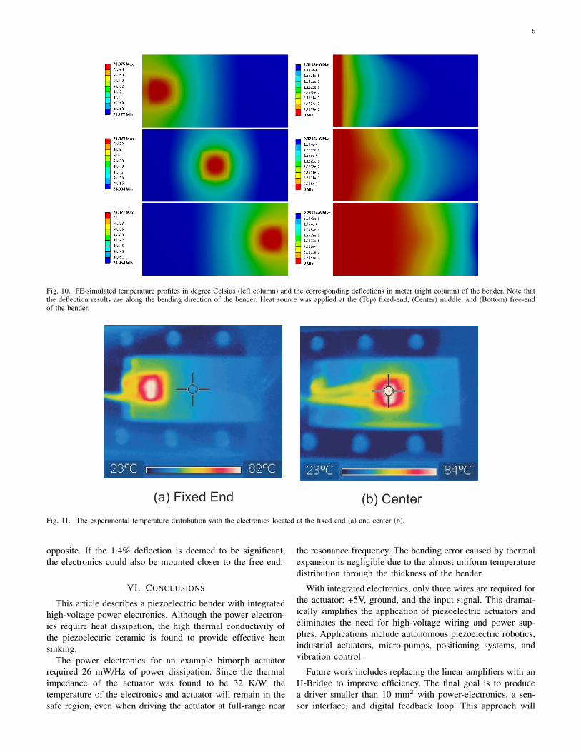
different locations: the fixed-end, the center, and the free-endof the bender.
Steady-state thermal analysis was first conducted on thepiezoelectric bender to simulate the temperature distribu-tion. The piezoelectric and brass layers were modeled usingSOLID90 elements. This element has 20 nodes with a singledegree-of-freedom (DOF), that is temperature, at each node.The thermal properties of the piezoelectric and brass layersare listed in Table II. The resulting temperature profiles areplotted in Fig. 10.
After finding the temperature profile, the results wereimported into the static structural analysis. In this analysissystem, the piezoelectric and brass layers were modeled usingSOLID186 elements. This element has 20 nodes with threeDOFs per node: translation in the nodal x, y and z directions.The FE-simulated temperature profiles and deflections due totemperature variations are plotted in Fig. 10.
Fig. 10 shows that the maximum and minimum temperaturesof the bender are very similar for all three heat sourcelocations. The estimated thermal impedances are 32.8 K/W,32.5 K/W and 32.2 K/W respectively for the heated fixed-end,middle and free-end of the bender. These estimated thermal
impedances are in close agreement with that of the analyticalvalue.
The simulated maximum deflection is approximately 2 µmalong the length of the bender for all three cases. Deflectionsalong the bending direction are two orders of magnitudesmaller than that of the longitudinal direction. It can beconcluded that the unwanted deflections due to heating canbe neglected. Since the thermal dissipation and deflection ofthe bender are not affected by the locations of the heat source,the power electronics can be located at the fixed-end of thebender which is a convenient choice.
V. EXPERIMENTAL RESULTS
To simulate the maximum feasible power dissipation, theactuator was driven at 100 Hz with a ±40 V sinusoid. Thisresulted in a supply current of 0.33 A from a 5 V supplywhich indicates a power dissipation of 1.65 W. The resultingtemperature profiles were recorded with a FLIR i3 infraredcamera.
The temperature profiles for the fixed-end and centrallymounted electronics are shown in Fig. 11. The maximumtemperatures were 82 ◦C and 84 ◦C respectively (with aroom temperature of 24 ◦C). Therefore, the thermal impedancewas 35 K/W for the fixed-end and 36 K/W for the centrallocation. These figures correlate well with the predicted ther-mal impedances of 32.8 K/W and 32.5 K/W. The slightlyhigher experimental impedance is due to the impedance of thebonding layer which is predicted to be approximately 6 K/W,this was not modeled in the FE analysis.
The position sensor described in Section II-C was calibratedto provide a sensitivity of 1.385 mm/V. The full displacementrange of the actuator (without power electronics) was mea-sured to be 2.4 mm (p-p) with a 5 Hz ±90 V sine waveinput. When the electronics were mounted in the middle ofthe actuator, the range was reduced by 5.8% to 2.26 mm.Similarly, when the electronics were located at the base, therange was reduced by 4.2% to 2.3 mm. These range reductionsare not considered to be significant since they are smaller thanthe range tolerance specified by the manufacturer. However,the range reduction could be reduced by using a thermalinterface material with greater elasticity.
To assess the thermally induced bending, the actuator fre-quency was increased until the input electrical power was1.65 W. After the temperature reached a maximum, the fre-quency was reduced to 5-Hz while monitoring the averagevalue of the position signal. A 24-mV change in the DCoffset was observed which corresponds to a thermally induceddeflection of 0.033 mm or 1.4% of the range. This is largerthan the FEA prediction of 0.1%. Since there is little temper-ature difference between the top and bottom surface of theactuator, the additional deflection is thought to be caused bythe thermal strain of the thermal interface material and PCB,which was not modeled in the FEA. The thermally inducedstrain of the electronics could be eliminated by mounting asecond amplifier on the bottom of the actuator. With the twoamplifiers connected in series, the dissipated power would beequal and the thermally induced strains would be equal and
6
Fig. 10. FE-simulated temperature profiles in degree Celsius (left column) and the corresponding deflections in meter (right column) of the bender. Note thatthe deflection results are along the bending direction of the bender. Heat source was applied at the (Top) fixed-end, (Center) middle, and (Bottom) free-endof the bender.
(b) Center(a) Fixed End
Fig. 11. The experimental temperature distribution with the electronics located at the fixed end (a) and center (b).
opposite. If the 1.4% deflection is deemed to be significant,the electronics could also be mounted closer to the free end.
VI. CONCLUSIONS
This article describes a piezoelectric bender with integratedhigh-voltage power electronics. Although the power electron-ics require heat dissipation, the high thermal conductivity ofthe piezoelectric ceramic is found to provide effective heatsinking.
The power electronics for an example bimorph actuatorrequired 26 mW/Hz of power dissipation. Since the thermalimpedance of the actuator was found to be 32 K/W, thetemperature of the electronics and actuator will remain in thesafe region, even when driving the actuator at full-range near
the resonance frequency. The bending error caused by thermalexpansion is negligible due to the almost uniform temperaturedistribution through the thickness of the bender.
With integrated electronics, only three wires are required forthe actuator: +5V, ground, and the input signal. This dramat-ically simplifies the application of piezoelectric actuators andeliminates the need for high-voltage wiring and power sup-plies. Applications include autonomous piezoelectric robotics,industrial actuators, micro-pumps, positioning systems, andvibration control.
Future work includes replacing the linear amplifiers with anH-Bridge to improve efficiency. The final goal is to producea driver smaller than 10 mm2 with power-electronics, a sen-sor interface, and digital feedback loop. This approach will

7
produce a true mechatronic system with all of the requiredcontrol and drive electronics. Another goal is to assess theimpact of thermal cycling on the fatigue life and performanceof the actuators.
ACKNOWLEDGEMENTS
This work was supported by the Australian Research Coun-cil Discovery Project DP0986319
REFERENCES
[1] Y. K. Yong, S. O. R. Moheimani, B. J. Kenton, and K. K. Leang, “Invitedreview article: High-speed flexure-guided nanopositioning: Mechanicaldesign and control issues,” Review of Scientific Instruments, vol. 83,no. 12, p. 121101, 2012.
[2] A. A. Eielsen, J. T. Gravdahl, and K. Y. Pettersen, “Adaptive feed-forward hysteresis compensation for piezoelectric actuators,” Review ofScientific Instruments, vol. 83, no. 8, p. 085001, 2012.
[3] E. Guliyev, T. Michels, B. Volland, T. Ivanov, M. Hofer, and I. Rangelow,“High speed quasi-monolithic silicon/piezostack spm scanning stage,”Microelectronic Engineering, vol. 98, no. 0, pp. 520 – 523, 2012.
[4] A. J. Fleming, “Nanopositioning system with force feedback for high-performance tracking and vibration control,” IEEE Transactions onMechatronics, vol. 15, no. 3, pp. 433–447, June 2010.
[5] K. Uchino and J. R. Giniewica, Micromechatronics. New York: MarcelDekker Inc., 2003.
[6] Y. Zhang, G. Liu, and J. Hesselbach, “On development of a rotary linearactuator using piezoelectric translators,” IEEE/ASME Transactions onMechatronics, vol. 11, no. 5, pp. 647–650, October 2006.
[7] P. Tenzer and R. Mrad, “A systematic procedure for the design ofpiezoelectric inchworm precision positioners,” IEEE/ASME Transactionson Mechatronics, vol. 9, no. 2, pp. 427–435, June 2004.
[8] R. Merry, N. de Kleijn, M. van de Molengraft, and M. Steinbuch, “Usinga walking piezo actuator to drive and control a high-precision stage,”IEEE/ASME Transactions on Mechatronics, vol. 14, no. 1, pp. 21–31,February 2009.
[9] Y. Takeuchi, Y. Sakaida, K. Sawada, and T. Sata, “Development ofa 5-axis control ultraprecision milling machine for micromachiningbased on non-friction servomechanisms,” CIRP Annals - ManufacturingTechnology, vol. 49, no. 1, pp. 295 – 298, 2000.
[10] L. D. Mauck and C. S. Lynch, “Piezoelectric hydraulic pump develop-ment,” Journal of Intelligent Material Systems and Structures, vol. 11,no. 10, pp. 758–764, 2000.
[11] M. Robiony, F. Polini, F. Costa, N. Zerman, and M. Politi, “Ultrasonicbone cutting for surgically assisted rapid maxillary expansion (sarme)under local anaesthesia,” International Journal of Oral and MaxillofacialSurgery, vol. 36, no. 3, pp. 267 – 269, 2007.
[12] D. Mehlfeldt, H. Weckenmann, and G. Sthr, “Modeling of piezoelectri-cally actuated fuel injectors,” Mechatronics, vol. 18, no. 56, pp. 264 –272, 2008.
[13] S. M. Salapaka and M. V. Salapaka, “Scanning probe microscopy,” IEEEControl Systems, vol. 28, no. 2, pp. 65–83, April 2008.
[14] G. Schitter, P. J. Thurner, and P. K. Hansma, “Design and input-shapingcontrol of a novel scanner for high-speed atomic force microscopy,”Mechatronics, vol. 18, no. 5-6, pp. 282–288, June 2008.
[15] Y. K. Yong, A. J. Fleming, and S. O. R. Moheimani, “A novel piezo-electric strain sensor for simultaneous damping and tracking control of ahigh-speed nanopositioner,” IEEE/ASME Transactions on Mechatronics,2012.
[16] B. J. Kenton, A. J. Fleming, and K. K. Leang, “A compact ultra-fast vertical nanopositioner for improving SPM scan speed,” Review ofScientific Instruments, vol. 82, no. 12, pp. 123 703(1–8), 2011.
[17] A. Preumont, Mechatronics, Dynamics of electromechanical and piezo-electric systems. Dordrecht, The Netherlands: Springer, 2006.
[18] S. S. Aphale, A. J. Fleming, and S. O. R. Moheimani, “Integral controlof resonant systems with collocated sensor-actuator pairs,” IOP Smartmaterials and Structures, vol. 16, pp. 439–446, April 2007.
[19] A. J. Fleming, “A method for measuring the resolution of nanoposition-ing systems,” Review of Scientific Instruments, vol. 83, no. 8, p. 086101,2012.
[20] G. M. Clayton, S. Tien, K. K. Leang, Q. Zou, and S. Devasia, “A reviewof feedforward control approaches in nanopositioning for high-speedSPM,” Journal of Dynamic Systems, Measurement, and Control, vol.131, pp. 061 101(1–19), November 2009.
[21] K. K. Leang, Q. Zou, and S. Devasia, “Feedforward control of piezoac-tuators in atomic force microscope systems,” IEEE Control Systems,vol. 29, no. 1, pp. 70–82, February 2009.
[22] H. Jiang, H. Ji, J. Qiu, and Y. Chen, “A modified prandtl-ishlinskiimodel for modeling asymmetric hysteresis of piezoelectric actuators,”Ultrasonics, Ferroelectrics and Frequency Control, IEEE Transactionson, vol. 57, no. 5, pp. 1200–1210, 2010.
[23] D. Wang, Q. Yang, and H. Dong, “A monolithic compliant piezoelectric-driven microgripper: Design, modeling, and testing,” IEEE/ASME Trans-actions on Mechatronics, vol. 18, no. 1, pp. 138–147, February 2013.
[24] B. Edamana and K. Oldham, “Optimal low-power piezoelectric actuatorcontrol with charge recovery for a microrobotic leg,” IEEE/ASMETransactions on Mechatronics, vol. 18, no. 1, pp. 251–262, February2013.
[25] R. Merry, M. Maassen, M. van de Molengraft, N. van de Wouw, andM. Steinbuch, “Modeling and waveform optimization of a nano-motionpiezo stage,” IEEE/ASME Transactions on Mechatronics, vol. 16, no. 4,pp. 615–626, August 2011.
[26] F. Levinzon, “Ultra-low-noise seismic piezoelectric accelerometer withintegral fet amplifier,” IEEE Sensors Journal, vol. 12, no. 6, pp. 2262–2268, June 2012.
[27] R. G. Ballas, Piezoelectric Multilayer Beam Bending Actuators. Berlin,Germany: Springer, 2007.
[28] PiezoDrive, “PDu100 datasheet,” www.piezodrive.com, 2012.[29] A. J. Fleming, “A review of nanometer resolution position sensors:
Operation and performance,” Sensors and Actuators A: Physical, vol.190, pp. 106–126, February 2013.
[30] H. J. M. T. A. Adriaens, W. L. de Koning, and R. Banning, “Modelingpiezoelectric actuators,” IEEE/ASME Transactions on Mechatronics,vol. 5, no. 4, pp. 331–341, December 2000.
[31] A. F. Mills, Heat Transfer, 2nd ed. Prentice Hall, Inc., 1999.[32] M. Toda, T. Ono, F. Liu, and I. Voiculescu, “Evaluation of bimaterial
cantilever beam for heat sensing at atmospheric pressure,” Review ofScientific Instruments, vol. 81, no. 5, p. 055104, 2010.