pic based dds for audio / lf g4jnt feb 2011g4jnt.com/pic_dds.pdf · page 1 pic based dds for audio...
TRANSCRIPT

Page 1
PIC Based DDS For audio / LF G4JNT Feb 2011
Switchable Coherent / FEK FSK version Annex AIQ Version added, March 2011. Details in Annex B
The module described implements a 32 bit Direct digital synthesizer using no more thana mid-range PIC microcontroller, external D/A converter and op-amp filter. It cangenerate frequencies up to about 40kHz maximum, or possibly higher if the device isoverclocked.
The PIC-16F628, contains a counter-timer that can be configured to generate an interruptwhen it overflows, and form the clock for a DDS implemented purely in software. Thecounter timer can be run from the processor’s internal clock signal which in turn isderived from the crystal or externally supplied oscillator. On the 16F family of devices ,the specification states this can be up to 20MHz, which is divided by four internally for amaximum processor clock of 5MHz. For LF and audio generation I wanted to be able togenerate at least the range of frequencies that a PC soundcard can manage, whichthese days means a sampling rate of at least 48kHz would be required, and a rate closerto 100kHz would be desirable. I also wanted to be able to generate audio tones ofvirtually any arbitrary frequency, so a 32 bit DDS architecture was considered necessary.
A DDS is no more than a counter that is incremented by a fixed value for each clockinput, rolls-over when it reaches maximum and starts counting again. The counter valueat each instant is used as the input to a sine lookup table. The resulting value looked-up from the table is sent to a Digital to Analogue (D/A) converter whose output, afterfiltering to remove clock and alias products is the wanted audio waveform. The valuethe counter is incremented each time is related to the wanted output frequency as follows:
A counter of length 32 bits rolls over every 232 counts, or each 4294967296 clocks. Thisdefines the underlying resolution or step size for the DDS. For a 100kHz input clock it istherefore 100kHz / 232 = 0.00002328Hz (23.3µHz) – fine enough for most purposes!The value by which the counter has to be incremented each time is then given by N =Fout / Fclock * 232 For an output of (almost) exactly 8.98kHz with a 100kHz clock N is8980/100000 * 232 = 385688063 or expressed in hexadecimal 0x16FD21FF.
The Algorithm
For a description, refer to the PIC source code listing basic_freqsource.asm whichcontains just the code for generating a single tone. The registers in the PIC are 8 bitswide so four are concatenated into a 32-bit accumulator, D3 through to D0. Four moreregisters, F3/2/1/0, hold the value N determining the frequency. Every interrupt cycle(at 100kHz for a 20MHz oscillator) the value in the F registers is added to theaccumulated D3 – D0 , which just overflows back to zero when its maximum count isreached. The most significant byte stored in D3 alone is then used as the address forthe sine look-up table. The resulting 8 bit value is placed on the PICs 8 bit paralleloutput Port-B.
The 32 bit addition, table lookup and output consume about 35 clock cycles within theinterrupt service routine, leaving little spare capacity.

Page 2
D/A Converter
A ladder made up of resistor pairs in the ratio of 1:2 makes a simple D/A converter. Theonly proviso is that each drive signal, or individual connection of the input word, mustswitch between zero volts and a fixed reference and have a negligibly low outputresistance when compared with the resistors making up the ladder. CMOS outputs,especially those on PIC devices, fulfil this requirement, switching between 0 V and Vcc(usually 5V) with about 10 ohms of internal resistance. So the 8-bit PORTB output fromthe PIC can directly drive the 16 1.8kΩ and 3.6kΩ resistors making up the chain at evenlower cost than a custom D/A chip.
Amplitude Resolution and Spurii
The restricted table-lookup capabilities of this baseline PIC family mean that tables withmore than 256 entries and more than an 8 bit output word are complicated to arrange,and would not fit into the limited amount of clock cycles I had allowed. However, forsimple audio and VLF purposes, the 8-bit DDS table would probably be adequate. Thereis a rule of thumb for all DSP that says spurious and quantising noise levels will lie atroughly 6.N dB below full scale, where N is the number of bits. So, very crudely andapproximately, an 8 bit lookup table ought to give about -48dBc spurious.
The DDS concept works best where output frequency is kept lower than a quarter of theclock. It cannot, in any case ever go above half the clock rate due to the Nyquistsampling criteria.
Output Filter
The D/A output now has to be filtered to remove alias products and spurii above 10kHz.A single stage, third order opamp filter can do the job admirably. The R-2R laddermaintains a constant output impedance of R - which here is set at 1.8kΩ - whateverthe output voltage. Biasing the output opamp filter and output levels ideally needs theoutput from the ladder to have its DC level raised and its 0-5V amplitude rangeattenuated. This is done by adding a 620Ω pull up resistor to 5V, through another 200ohms decoupled to prevent noise of the 5V rail appearing directly in the audio path. Theresult is an output impedance of 461 ohms and a peak – peak waveform amplitude of1.28V superimposed on a mean DC level of 3.44V The first stage of filtering comes fromthe 22nF capacitor from between the output of the resistor ladder to ground for a firststage cutoff at 15.6kHz The opamp filter, whose values are taken from standard tableshas an underlying gain of 2.1 times, resulting in an output of 2.7V peak-peak, or veryclose to 1V RMS. The values shown give a cut-off at 10kHz, but a higher frequencywould be possible by proportionally reducing the value of the two 1nF capacitors and/orthe 18k resistors if some degradation in spurii at the upper frequency band is accepted.
Results
Page 3
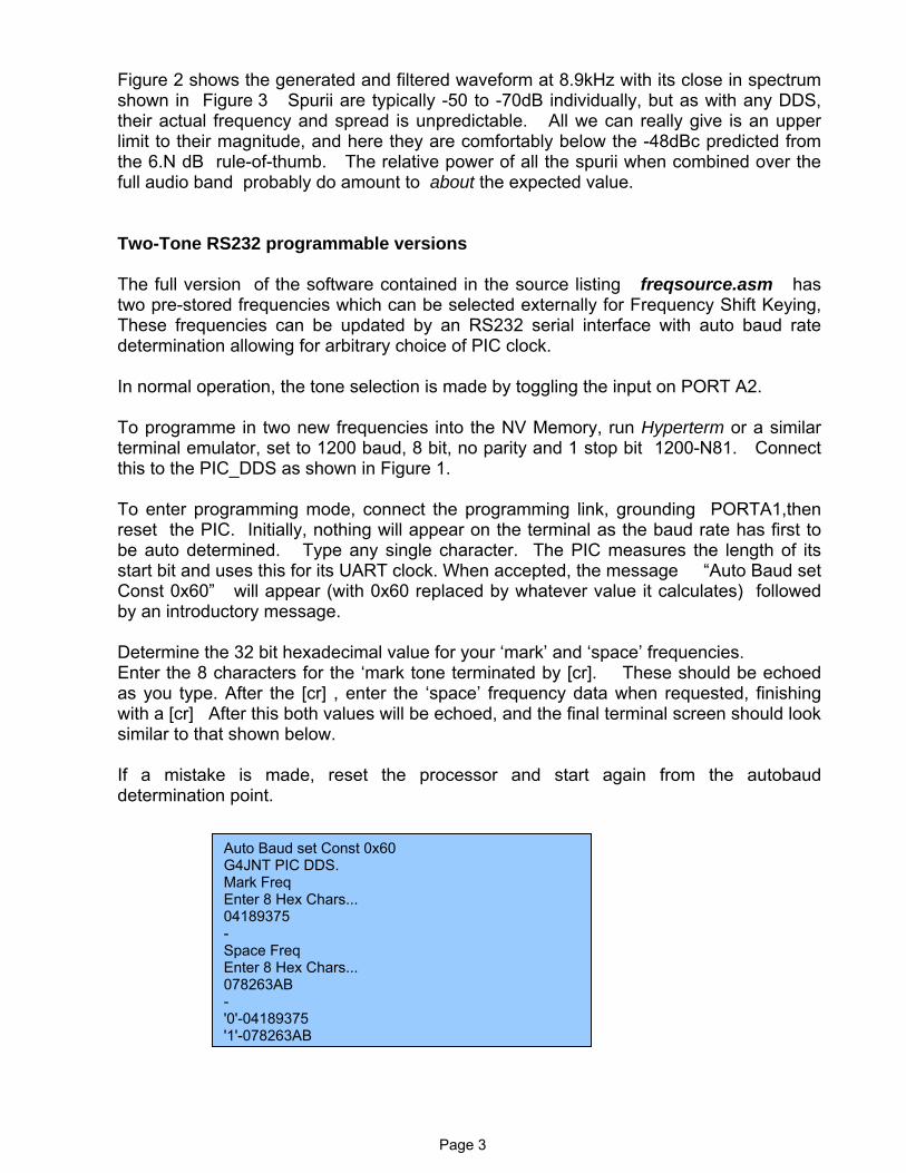
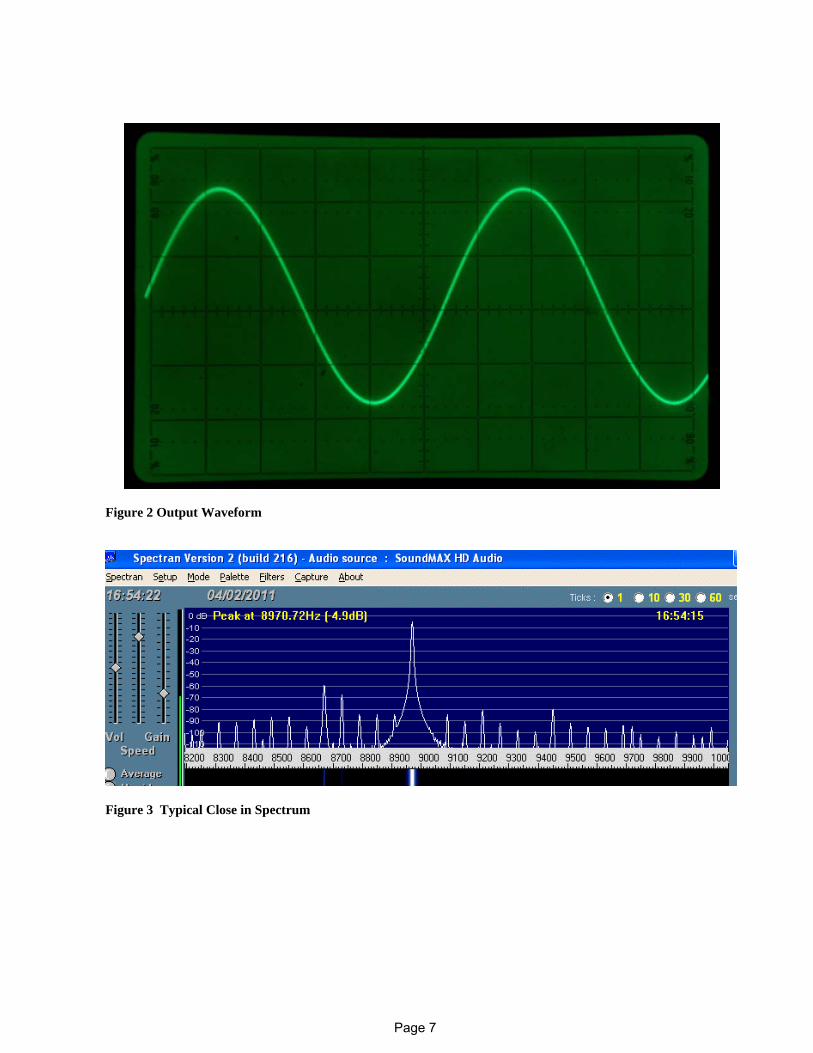
Figure 2 shows the generated and filtered waveform at 8.9kHz with its close in spectrumshown in Figure 3 Spurii are typically -50 to -70dB individually, but as with any DDS,their actual frequency and spread is unpredictable. All we can really give is an upperlimit to their magnitude, and here they are comfortably below the -48dBc predicted fromthe 6.N dB rule-of-thumb. The relative power of all the spurii when combined over thefull audio band probably do amount to about the expected value.
Two-Tone RS232 programmable versions
The full version of the software contained in the source listing freqsource.asm hastwo pre-stored frequencies which can be selected externally for Frequency Shift Keying,These frequencies can be updated by an RS232 serial interface with auto baud ratedetermination allowing for arbitrary choice of PIC clock.
In normal operation, the tone selection is made by toggling the input on PORT A2.
To programme in two new frequencies into the NV Memory, run Hyperterm or a similarterminal emulator, set to 1200 baud, 8 bit, no parity and 1 stop bit 1200-N81. Connectthis to the PIC_DDS as shown in Figure 1.
To enter programming mode, connect the programming link, grounding PORTA1,thenreset the PIC. Initially, nothing will appear on the terminal as the baud rate has first tobe auto determined. Type any single character. The PIC measures the length of itsstart bit and uses this for its UART clock. When accepted, the message “Auto Baud setConst 0x60” will appear (with 0x60 replaced by whatever value it calculates) followedby an introductory message.
Determine the 32 bit hexadecimal value for your ‘mark’ and ‘space’ frequencies.Enter the 8 characters for the ‘mark tone terminated by [cr]. These should be echoedas you type. After the [cr] , enter the ‘space’ frequency data when requested, finishingwith a [cr] After this both values will be echoed, and the final terminal screen should looksimilar to that shown below.
If a mistake is made, reset the processor and start again from the autobauddetermination point.
Auto Baud set Const 0x60G4JNT PIC DDS.Mark FreqEnter 8 Hex Chars...04189375-Space FreqEnter 8 Hex Chars...078263AB-'0'-04189375'1'-078263AB

Page 4
From now on, the DDS should start generating a waveform. Remove the RS232interface and the programming link, and use the serial input connection to togglebetween the two tones which have now been stored.
Coherent Two-Tone version
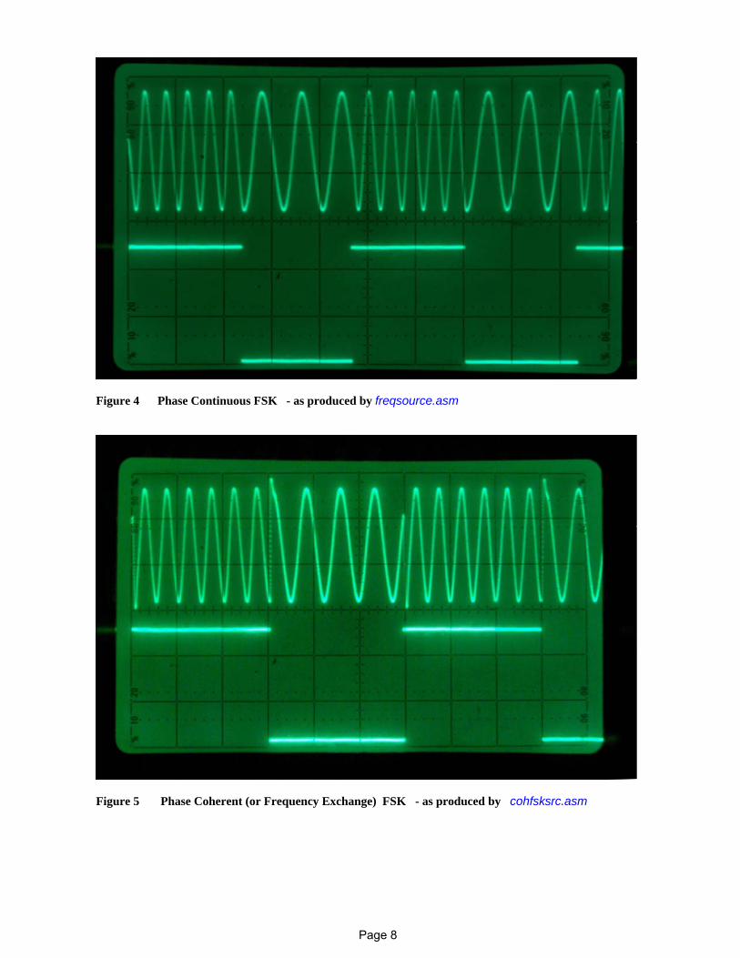
As an alternative to switching between two tones by changing the incremental value,another way of generating FSK is to switch between two continuously running oscillators.This has the advantage that each tone maintains phase coherency, allowing optimumdecoding when used for weak signalling. But does mean there is a discontinuity astones are switched with no phase-coherency in the resulting waveform.
In a DDS two frequencies can be maintained in this way by having two accumulators,each updated by their own frequency register. The output from one or the other is thenused as the address for the sine-lookup table There are twice as many instructionsneeded in the dual 32 bit addition, and the PIC cannot run so fast. However, it is stillpossible to manage both in 64 clock cycles and the PIC code contained incohfsksrc.asm offers an alternative two-tone generator based on a clock running atFosc / 256.
PIC Frequency Source
The PIC is configured for HS, or High Speed, oscillator, and in this form will acceptalmost any waveform supplied to the OSCIN connection with a level of a few hundredsmillivolts RMS Although the chip is rated to 20MHz it appears to be capable of beingover clocked up to at least 40MHz
In the phase continuous two tone version, the DDS clock frequency is equal to theOscillator input / 160. So for a 10MHz input, the DDS is clocked at 62.5kHz. For a20MHz input the clock is 125kHz. (Note that in the simple single tone version, a largerdivision ratio is used with the DDS clock being 1/200 of the input frequency)
For the dual tone version, the clock is 1/256 of the input frequency, so for 10MHz input itis 39062.5Hz, and for 20MHz input, 78.125kHz.
PCB Layout
Copper patterns for the single sided surface mount PCB shown in the photograph belowcan be found in the .PDF files for home construction. Choose the version most suitablefor your purposes, both standard and mirrored versions are given, at 1:1 and 2:1 scales.Component placement should be straightforward enough by following the circuit diagramand photograph.

Page 5
PIC Code
For maximum flexibility and understanding, try to assemble and programme the three.ASM files. If you can only programme devices and do not wish to, or are unable, toassemble the source code, the .hex files can be used on their own.
Full Construction Archive
A full archive with PCB layouts and PIC code source and .HEX format can be found at
http://www.g4jnt.com/PIC_DDS.zip
Photo 1 The PIC_DDS Module SMT Printed Circuit Board

Page 6
Figure 1 Circuit Diagram
Page 7
Figure 2 Output Waveform
Figure 3 Typical Close in Spectrum
Page 8
Figure 4 Phase Continuous FSK - as produced by freqsource.asm
Figure 5 Phase Coherent (or Frequency Exchange) FSK - as produced by cohfsksrc.asm

Page 9
Annex A Switchable Coherent / Non-coherent FSK
PIC Code FSKDDS.ASM combines both FSK Generation schemes into a singleswitchable source. Another line is added to PIC PORTA, 4 on pin 3 of the 16F628. Adda third 22k pull up resistor to +5V.
When pulled high Coherent, or Frequency Exchange, keying is generated, exactly as forcohfsksrc described above. The sampling rate remains the same at 1/256 Fin,
When A4 is pulled low, the keying changes immediately to continuous mode similar tothat described for freqsource.asm but note that for ease of use, the sampling ratestays at 1/256 Fin so no change in output frequency occurs when the mode is toggled.
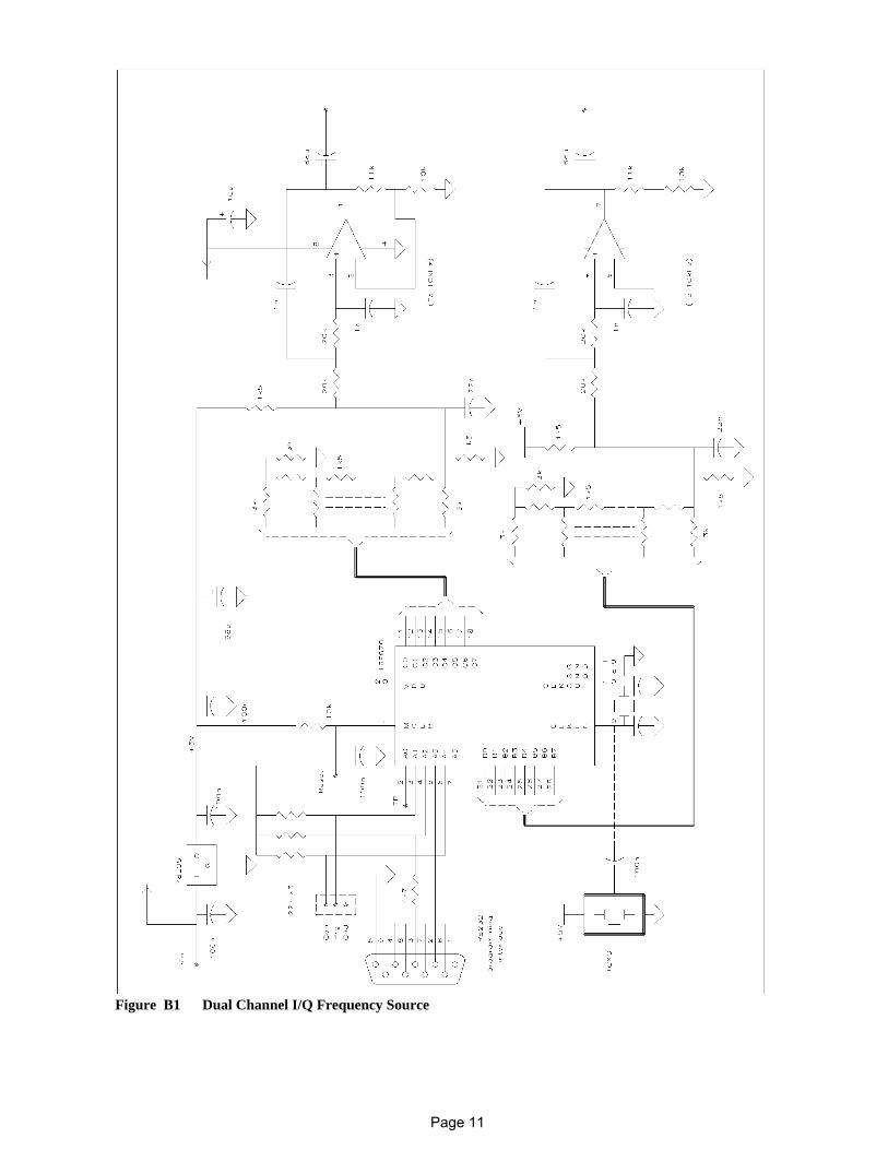
Annex B Dual Channel Version with IQ outputs
Figure B1 shows the circuit diagram of a version of the dual mode FSK source using the16F870 PIC with dual D/A converters and filters to generate 90º I/Q channels forapplication in direct image cancelling RF Upconversion. The software is contained inthe PIC code FSKDDSIQ.ASM which has identical functionality to FSKDDS. The linksfor serial programming and Continuous / FEK , as well as the RS232 connections are onthe same A1 – A4 connections as for the 16F628 version. PORTB forms the 8 bitsgoing to the I channel D/A converter. The additional PORTC goes to the identicalsecond, Q, channel.
To accommodate additional clock cycles in the interrupt routine for two calls to the sinelookup table and the additional port write, the sampling rate has had to be reduced toFosc/320. So for a 19.6608MHz crystal, Fs still remains an acceptable 61440Hz. At10MHz input, Fs is now 31250Hz; more than satisfactory for audio tone generation, butnow becoming a bit marginal at 10kHz output.
To cater for this, the cutoff frequency of the output filter has been reduced by 10% . Thefilter has also been reconfigured so that, apart from the lower limit set by the outputcapacitors (which can be removed if care is taken with subsequent DC ouput currentcapability and voltage offsetting) otherwise gives a frequency response extending downto true DC. Output amplitude is 3.5V peak-peak, or just over 1.2V RMS
PCB Layout
Copper patterns for the single sided surface mount PCB can be found in the .PDF filesfor home construction.

Page 10
Choose the version most suitable for your purposes, both standard and mirrored versionsare given, at 1:1 and 2:1 scales.
Component placement should be straightforward enough by following the circuit diagram.
The 16F870 PIC is in a 28 PIN DIL package, and sits on the 28 rectangular pads withPin 1 at the top of the diagram shown in Fig B2.
Page 11
Figure B1 Dual Channel I/Q Frequency Source

Page 12
Figure B2 PCB Layout