pic 18 microcontroller
TRANSCRIPT

PIC-18 MICROCONTROLLER
Under the Guidence of Mr. ROHITH.S
PRESENTED BY:-
1. ASHISH RANJAN (9008149020)
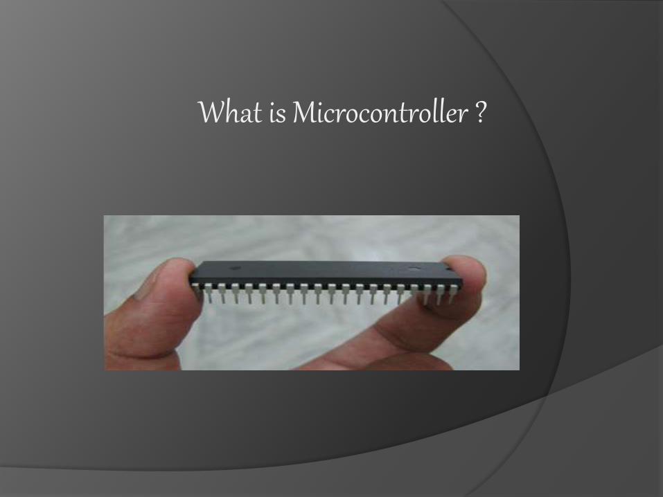
What is Microcontroller ?
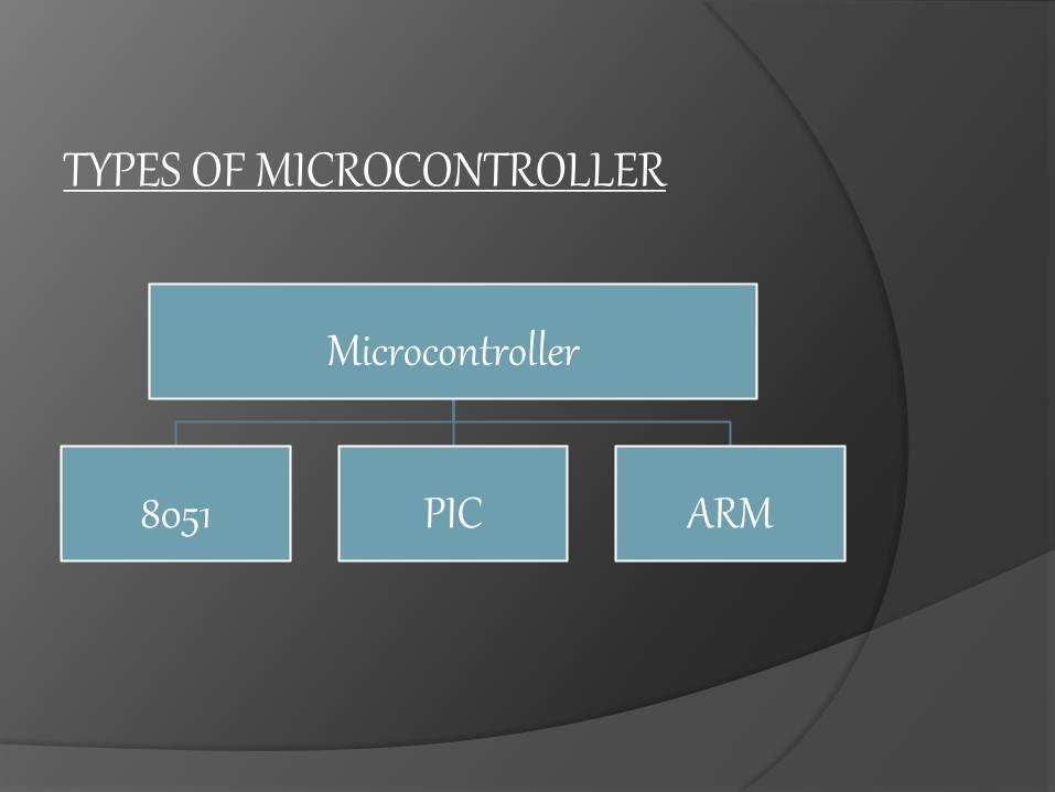
Microcontroller
8051 PIC ARM
TYPES OF MICROCONTROLLER
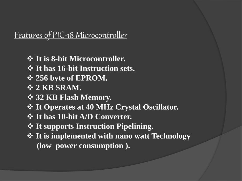
Features of PIC-18 Microcontroller
It is 8-bit Microcontroller.
It has 16-bit Instruction sets.
256 byte of EPROM.
2 KB SRAM.
32 KB Flash Memory.
It Operates at 40 MHz Crystal Oscillator.
It has 10-bit A/D Converter.
It supports Instruction Pipelining.
It is implemented with nano watt Technology
(low power consumption ).

PIN DIAGRAM OF PIC-18 MICROCONTROLLER
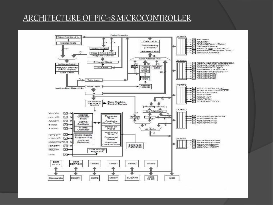
ARCHITECTURE OF PIC-18 MICROCONTROLLER
PIC-18 ADDRESSING MODES
Register Direct : Use an 8-bit value to specify a data register.
Ex:- movwf 0x20,A ; the value 0x20 is register direct mode
Immediate Mode : A value in the instruction to be used as an operand.
Ex:- addlw 0x10 ; add hex value 0x10 to WREG
movlw 0x30 ; load 0x30 into WREG
Inherent Mode : an implied operand.
Ex:- andlw 0x3C ; the operand WREG is implied
daw ; the operand WREG is implied
Indirect Mode : A special function register (FSRx) is used as a pointer to
the actual data register.
Ex:- movwf INDFx (where x = 0,1,2,3)
PIC-18 MEMORY ORGANIZATION
Data Memory and Program Memory are separated.
Separation of Data memory and Program memory makes possible the
the simultaneous access of data and instruction.
Data memory are used as general purpose registers or special function
registers.
On-chip Data EPROM are provided in some PIC-18 MCUs

Separation of Data Memory and Program Memory
Program
Memory
Space
PIC-18
CPU
21-bit program
address
16-bit
instruction bus
Data
Memory
Space
12-bit Register
address
8-bit Data Bus
Fig:- The PIC-18 Memory Spaces
PIC-18 DATA MEMORY
It consist of General purpose register and Special function registers.
Both are referred to as Data Registers.
PIC-18 has 4KB Data Memory.
Data Memory is Divided into Banks and each Bank has 256 bytes.
General purpose registers are used to hold dynamic data.
Special function register are used to control the Operation of Peripheral functions.
Only on bank is active at any time.
It implement access bank to reduce problem caused by bank switching.
Access bank Consists of the lowest 96 bytes and the highest 160 bytes of the data
memory space.
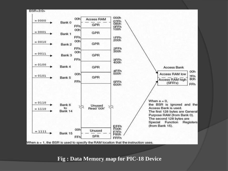
Fig : Data Memory map for PIC-18 Device

PROGRAM MEMORY ORGANIZATION
The program counter (PC) is 21-bit long, which enables the user program to
access up to 2MB program memory.
After Power On it starts to execute the instruction from address 0.
The Location 0x08 is reserved for high-priority interrupt service routine.
The Location 0x18 is reserved for low-priority interrupt service routine.
Up to 128 KB of Program Memory is inside the MCU chip.
Rest Part of the program memory is located outside of the MCU chip.
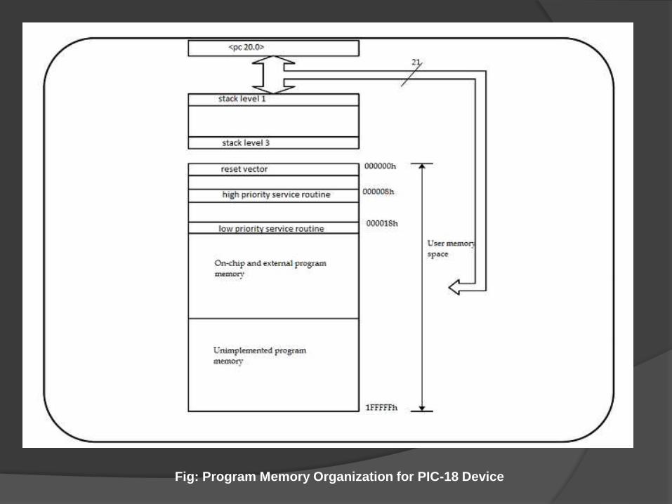
Fig: Program Memory Organization for PIC-18 Device

PIC-18 PIPELINING The PIC18 Divide most of the instruction execution into two
stages: instruction fetch and instruction execution.
Up to two instructions are overlapped in their execution. One instruction
is inexecution fetch stage while the second instruction is in execution stage.
Because of pipelining, each instruction appears to take one instruction
cycle to complete.
Fetch 2
Execute 1
Fetch 4
Fetch 3
Fetch 1
Execute 2
Execute 3
Execute sub_1Fetch sub_1
Flush
TCY0 TCY1 TCY2 TCY3 TCY4 TCY5
Fig : An Example of Instruction Pipeline flow

THANK YOU…..