pic 12f629/675
DESCRIPTION
PIC 12F629/675. “Wide variety”. 8-84 pin RISC core, 12/14/16bit program word USART/AUSART, I 2 C, ADC, ICSP, ICD OTP/UV EPROM/FLASH/ROM Families: PIC12, PIC16, PIC17, PIC18. Highlights. 14bit program word 1792Bytes (1024k words) FLASH program memory (10 5 e/w) 64Bytes 8-bit RAM - PowerPoint PPT PresentationTRANSCRIPT

PIC12F629/675


“Wide variety”
• 8-84 pin
• RISC core, 12/14/16bit program word
• USART/AUSART, I2C, ADC, ICSP, ICD
• OTP/UV EPROM/FLASH/ROM
• Families: PIC12, PIC16, PIC17, PIC18
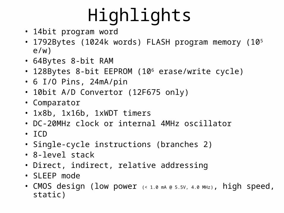
Highlights• 14bit program word• 1792Bytes (1024k words) FLASH program memory (105 e/w)• 64Bytes 8-bit RAM• 128Bytes 8-bit EEPROM (106 erase/write cycle)• 6 I/O Pins, 24mA/pin• 10bit A/D Convertor (12F675 only)• Comparator• 1x8b, 1x16b, 1xWDT timers• DC-20MHz clock or internal 4MHz oscillator• ICD• Single-cycle instructions (branches 2)• 8-level stack• Direct, indirect, relative addressing• SLEEP mode• CMOS design (low power (< 1.0 mA @ 5.5V, 4.0 MHz), high speed, static)

Blokové schema

Registers• 2 banks, switch via STATUS<5>
• Special Function Regs– 00h-1Fh – Core– Peripheral
• General Purpose Regs– 20h-5Fh / A0-DFh– Mapped bank1bank0
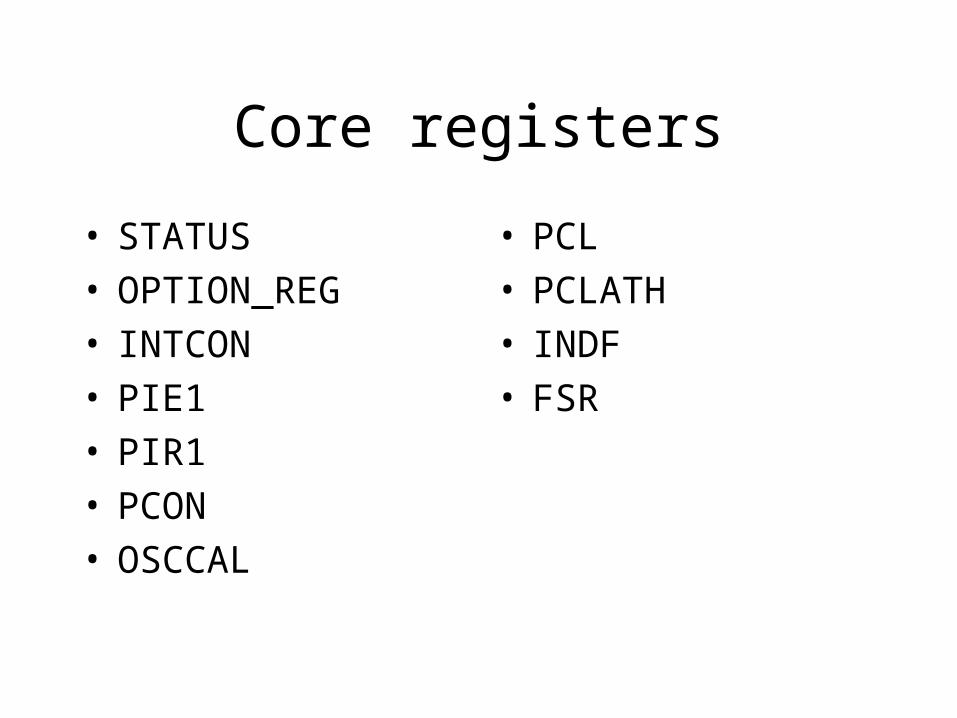
Core registers
• STATUS• OPTION_REG• INTCON• PIE1• PIR1• PCON• OSCCAL
• PCL• PCLATH• INDF• FSR

Peripherals
• GPIO GPIO, TRISIO, WPU, IOCB
• TIMER0 8bit
• TIMER1 16bit, timer/async.counter/sync.counter
• COMPARATOR internal reference, output
• A/D 4x10bit multiplexed, available during SLEEP bias reduce
• EEPROM 128B, auto erase-before-write

Features I• Configuration word• Oscilator DC-20MHz
– LP,XT,HS– RC (CLKOUT/IO)– INTOSC (CLKOUT/IO) 4MHz
– EC
• Reset– MCLR Master Clear– POR Power-on Reset– PWRT Power-up Timer 72ms
– OST Oscillator Start-up Timer 1024c after PWRT
– BOD Brown-out Detect
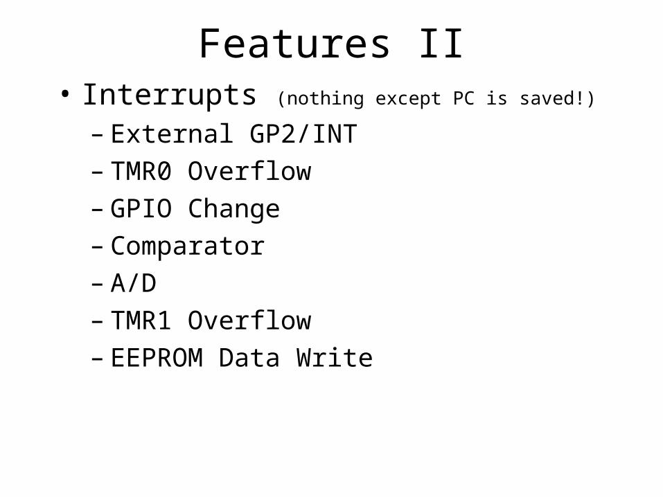
Features II• Interrupts (nothing except PC is saved!)
– External GP2/INT– TMR0 Overflow– GPIO Change– Comparator– A/D– TMR1 Overflow– EEPROM Data Write

Features III• Watchdog Timer
• SLEEP
• Code Protection• ID Location 2000h-2003h
• IN CIRCUIT SERIAL PROGRAMMING

Features IV• Power
– <=4MHz• 2.0-5.5V (A/D off, -40°C-85°C)
• 2.2-5.5V (A/D on, 0°C-85°C)
• 2.5-5.5V (A/D on, -40°C-85°C)
– 4-10MHz• 3.0-5.5V (0°C-85°C)
– >10MHz• 4.5-5.5V (-40°C-125°C)
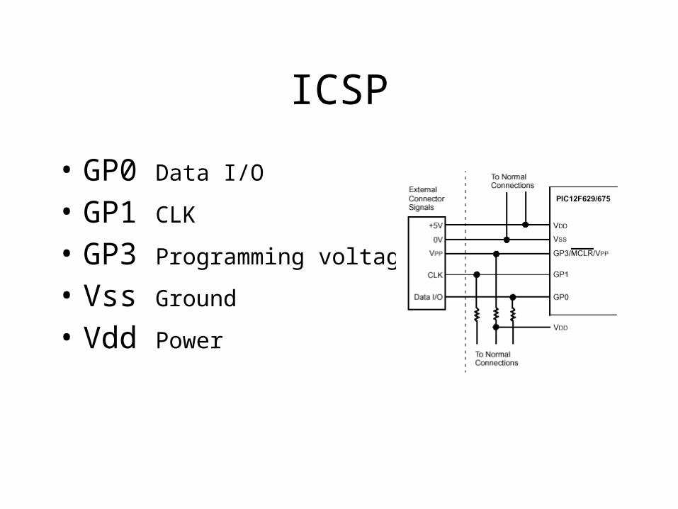
ICSP
• GP0 Data I/O
• GP1 CLK
• GP3 Programming voltage
• Vss Ground
• Vdd Power
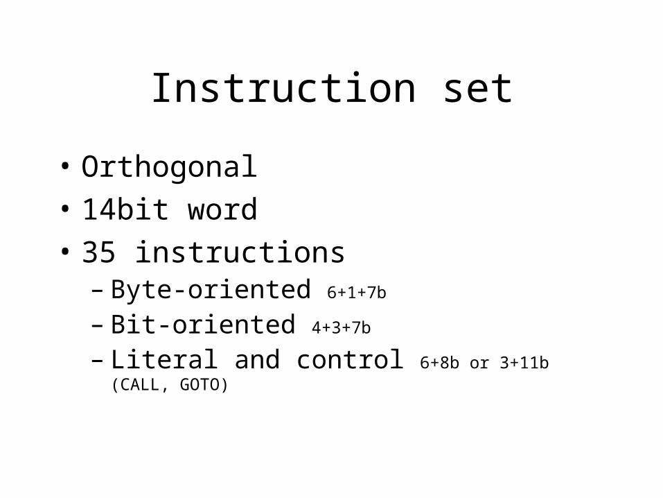
Instruction set
• Orthogonal
• 14bit word
• 35 instructions– Byte-oriented 6+1+7b
– Bit-oriented 4+3+7b
– Literal and control 6+8b or 3+11b (CALL, GOTO)

• f … registr 00h-7Fh
• d … destination 0=W, 1=f
• b … bit address 0-7
• k … literal
• Flags C,DC,Z

Byte-oriented
• ADDWF f,d• ANDWF f,d• CLRF f• CLRW• COMF f,d• DECF f,d• DECFSZ f,d• INCF• INCFSZ f,d
• IORWF f,d• MOVF f,d• MOVWF f• NOP• RLF f,d• RRF f,d• SUBWF f,d• SWAPF f,d• XORWF f,d

Bit-oriented
• BCF f,b• BSF f,b• BTFSC f,b• BTFSS f,b

Literal and Control
• ADDLW k• ANDLW k• CLRWDT• IORLW k• MOVLW k• SUBLW k• XORLW k
• CALL k• GOTO k• RETFIE• RETLW k• RETURN• SLEEP