phytek confidential 1 2015/7/17 - sitri confidential 2 ... ×600 (w) ×700 (d) mm weight: about...
TRANSCRIPT

2015/7/17 1 PHYTEK Confidential
2015/7/17 2 PHYTEK Confidential
◆ Product name
SoC Tester Alpha7L
◆ Features
With test pattern generator which has both properties, logic
test pattern generator and memory tester one, the flexible
test is possible. And multi measurement is possible.
◆ Electrical Specifications
Fast Digital I/O pin
Per-pin Architecture 100MHz max
VIH/L, VOH/L, IOH/L, VT, PMU, Timing, and so on
TMU : 4 per IO board, 250MHz ◆ Number of fast digital I/O pins
1,024 pins standard ( 2,048 pins is possible) ◆ Infrastructure Specification
consumption electric power : 5KVA(220V single phase)
Size 679(H)×720(W)×800(D) mm
(Main body only : Cable excludes)
Weight About 250kg
size of Rack for PC: 740 (H)×600 (W) ×700 (D) mm
weight: about 70Kg
air: pressure MAX 0.6Mpa amount 50L/Min
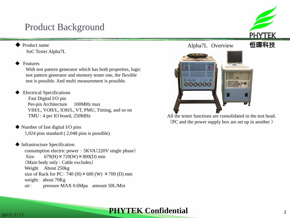
Product Background
Alpha7L Overview
All the tester functions are consolidated in the test head.
(PC and the power supply box are set up in another )
2015/7/17 3 PHYTEK Confidential
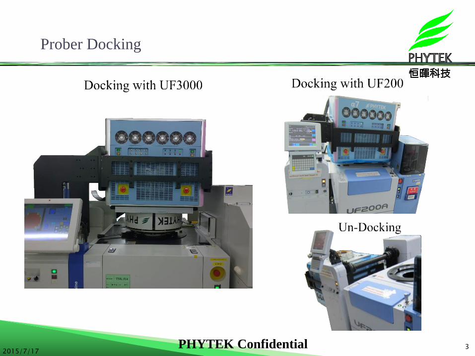
Prober Docking

2015/7/17 4 PHYTEK Confidential
Specification of Tester
TGROUP 0
Except TGROUP 0
VIH
VIL
Amplitude
VOH, VOL
Termination mode
Active Load IOH/IOL
PMU per PIN
DPS
Alpha7L
32
Main CPU and Sub-CPU (The realized reduction the test time in the sub-
CPU)
64 pins per IO board
50MHz / 100MHz ( 500ps / 250ps)
4 Edge
ITEMS
Timing Dead Zone
Test Pin
Configurations
Par pin set
Timing Group
PINS
Controller
Timing Edge
Frequency ( Period Resolution )
Clock
Resolution
Multi DUT test
Relay Control
Timing Skew
DC
Configurations
LPG Pattern Length
Instructions
Measure Frequency and Time Period
Buffer Memory (Writing data memory)
Fail bit Counter
Fail Memory
Subroutine Pattem Memory
ALPG, Data Generation (Option)
AD/DA (Option)
ROM Pattern Memory (Option)
32M / 50MHz , 42M / 100MHz, option to 128M
- 1.5 V ~ + 6.5 V, ± 30 mA (PMU/ Pin)
8K Record
4ch per IO board. 250MHz
1 K Vector
1-set/ 1pin(1024pin system has 1024-set)
16 Logic Pattern Generation Instruction
2 K Vector
4K x 64bit
4 G x 64 I/O ( X16, Y16, Z8), NOR & NAND supported
AWG 16bit/50KHz, Digitizer 16bit/250KHz
64 pins per IO board
16 Memory Pattern Generation Instruction(option)
100 ps
256
8 channel per IO board
NA
0.05 V ~ 8.00 VP-P
- 1.50 V ~ + 6.45 V
- 1.45 V ~ + 6.50 V , Hi Volt mode 13 V (1 MHz )
± 500 ps
1.0 ns
50 ohm
- 1.5 V ~ + 6.5 V (Dual Comparator)
0 ~ ± 20 mA

2015/7/17 5 PHYTEK Confidential
◆Pin Electronics on per-pin method Feature 1
PMU
Edge 1~4
VIH/VIL
VOH/VOL
Fail Counter
Active Load
Comparator
Driver
PMU
Edge 1~4
VIH/VIL
VOH/VOL
Fail Counter
Active Load
Comparator
Driver
PMU
Edge 1~4
VIH/VIL
VOH/VOL
Fail Counter
Active Load
Comparator
Driver
PMU
Edge 1~4
VIH/VIL
VOH/VOL
Fail Counter
Active Load
Comparator
Driver
PMU
Edge 1~4
VIH/VIL
VOH/VOL
Fail Counter
Active Load
Comparator
Driver
PMU
Edge 1~4
VIH/VIL
VOH/VOL
Fail Counter
Active Load
Comparator
Driver
PMU
Edge 1~4
VIH/VIL
VOH/VOL
Fail Counter
Active Load
Comparator
Driver
PMU
Edge 1~4
VIH/VIL
VOH/VOL
Fail Counter
Active Load
Comparator
Driver
Per-pin Structure (The following functions
are loaded at each pin.)
PMU (High speed DC test is realized.)
4 Edge Generator (5bit/vector control)
VIH,VIL (Changeable at each pin)
VOH,VOL (Changeable at each pin)
IOH,IOL (Changeable at each pin)
Active Load
50Ω Terminal
Relay Control
PMU
Edge 1~4
VIH/VIL
VOH/VOL
Fail Counter
Active Load
Comparator
Driver
PMU
Edge 1~4
VIH/VIL
VOH/VOL
Fail Counter
Active Load
Comparator
Driver
PMU
Edge 1~4
VIH/VIL
VOH/VOL
Fail Counter
Active Load
Comparator
Driver
PMU
Edge 1~4
VIH/VIL
VOH/VOL
Fail Counter
Active Load
Comparator
Driver

2015/7/17 6 PHYTEK Confidential
Driver Waveform at every Amplitude (Setting of Output Voltage:0V-2V, 4V, 6V)
25ns
1ns
Trigger Point
Measurement of Timing Jitter at the next period
(Trigger Point : Last Period)
Measurement of Timing Jitter (Setting of Output Voltage :0V-1.0V)
Enlargement of above point
25ns
1ns
Feature 2
The Minimum Pulse Width and Timing Linearity
(Setting of Output Voltage:0V-1.0V) Delay Tap : 250psec
◆ Having the capacity of generating the
pattern of 100MHz(200Mbps) and
1Gbps as option.
(Skew±50ps with Paired pin)
◆Pulse Drive with low amplitude and high
amplitude under 13V Drive are possible.
◆Low Jitter design(100ps)

2015/7/17 7 PHYTEK Confidential
◆ The processing speed is raised with built-in distributed processor with every 64ch. ◆ The great many test at one time is possible with the function of parallel test to
large number.
The function of distributed processor
1.Being high-speed in setting the test condition(Process time is shorten for about 5~10%) The host PC does not perform the set a large number of timing, voltage, and current. It is performed with dispersed processor located on every measurement boards.
2.DC test process (Process time is shorten for about 5~10%) DC test process at logic I/O pin is performed with dispersed processor.
3. IDDQ test process (Process time is shorten for about 5~10%) The dispersed processor makes a role with processing the histogram of IDDQ value, average, and detecting the maximum value and the minimum one.
4.Processing when all numbers are measured at the same time.
Feature 3

2015/7/17 8 PHYTEK Confidential
Main CPU
Array CPU
IO
IO
IO
DPS
Main CPU
IO
IO
DPS
DPS
DP
DP
DP
Traditional Tester Alpha7L advanced Architecture
DP : Distributed Processor
2 5 24
1
32CPU
1
1
2CPU
IO
DPS

2015/7/17 9 PHYTEK Confidential
◆ Achieved the flexible pin architecture to 1,024 pins.
◆ Because both functions, LPG(Logic Pattern Generator) and ALPG(Memory Pattern
Generator), are loaded, the 1 Pass test is possible. ◆ Possible to work independently LPG, ALPG and Period Timing with every from 64pins to
1,024pins.
Feature 4
PC for control
Relay control
Address Se lector(32 c ircu its)
Memory forROM Test(MAX8G)
Buffer Memory(2k Vector )
Fai l Memory(8k Record)
64 I/O
Relay Control (64CH)
Site Board
LPG
ALPG
Available as I/O for test too
Fai lCounter PMU
FormatPara l l elSeri a l
Converter
Judge
Edge 1
Edge 2
Edge 3
Edge 4P
in E
lectro
nic
s
8 VPS
TG32 Timing
GroupMAINOSC
MCU
DRAM
I/F
VIH/VIL
4 edge/pin
Act iveLoad

2015/7/17 10 PHYTEK Confidential
◆Equipped AWG and DGTZ with multi-channels. (It is possible to change for 4 VPS in 8 ones located in every 64 pins to AWG or DGTZ.) (Under 1024 pins system ,it is possible to equip 128 channels in the max.)
The function of AWG (50Kbps)and that of DGTZ are loaded.(250Kbps)
Feature 5
2015/7/17 11 PHYTEK Confidential
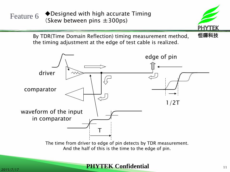
By TDR(Time Domain Reflection) timing measurement method, the timing adjustment at the edge of test cable is realized.
◆Designed with high accurate Timing (Skew between pins ±300ps)
T
1/2T
waveform of the input in comparator
edge of pin
driver
comparator
The time from driver to edge of pin detects by TDR measurement. And the half of this is the time to the edge of pin.
Feature 6

2015/7/17 12 PHYTEK Confidential
◆ We achieved low cable capacity, 60pF, by being wired in the shortest.
Other maker’s test head The board location of test head
in Alpha7L
Micro-Pin Tower
The tester board is located roundly, and wire length to probe card is
Shortest (59cm). From this method, the transmitting quality of signal
is improved (speed-up of judge).
Feature 7

2015/7/17 13 PHYTEK Confidential
◆ The annual electricity power cost is reduced for
3 million yen compared with the other companies. (1,024 pins)
Differential annual electric power cost:10KVA×22yen/hour×24hours×365days≒2 million yen
Differential annual air conditioning cost :2 million yen/2=1 million yen Total is 3 million yen.
*The difference of electric power with the other companies tester is supposed 10KVA.
◆Installation area is 1/2 compared
with other makers.
◆ A low consumption power is achieved
The an annual cost is greatly saved.
◆ Making to low space is achieved(No footprint design).
The installation area and power consumption are reduced much more than other makers.
Because the board is equipped with all tester functions.
Feature 8
Other Companies+Prober
1.5m2 WS PC
3.78m2
Prober
3.0m
2.7m
5.0m
Area for Maintenance
Installation Area=25m2
Alpha7L +Prober
Installation Area =12.5m2
Passage
Alpha7L Prober
Power Supply+PC
2.5m
5.0m
3.78m2
Other
Companies
Tester
Cooling device machine +
Piping area

2015/7/17 14 PHYTEK Confidential
Operation Software with usability (part1)
Shmoo Plot Channel Information
Wave Format
Distribution Plot
2015/7/17 15 PHYTEK Confidential
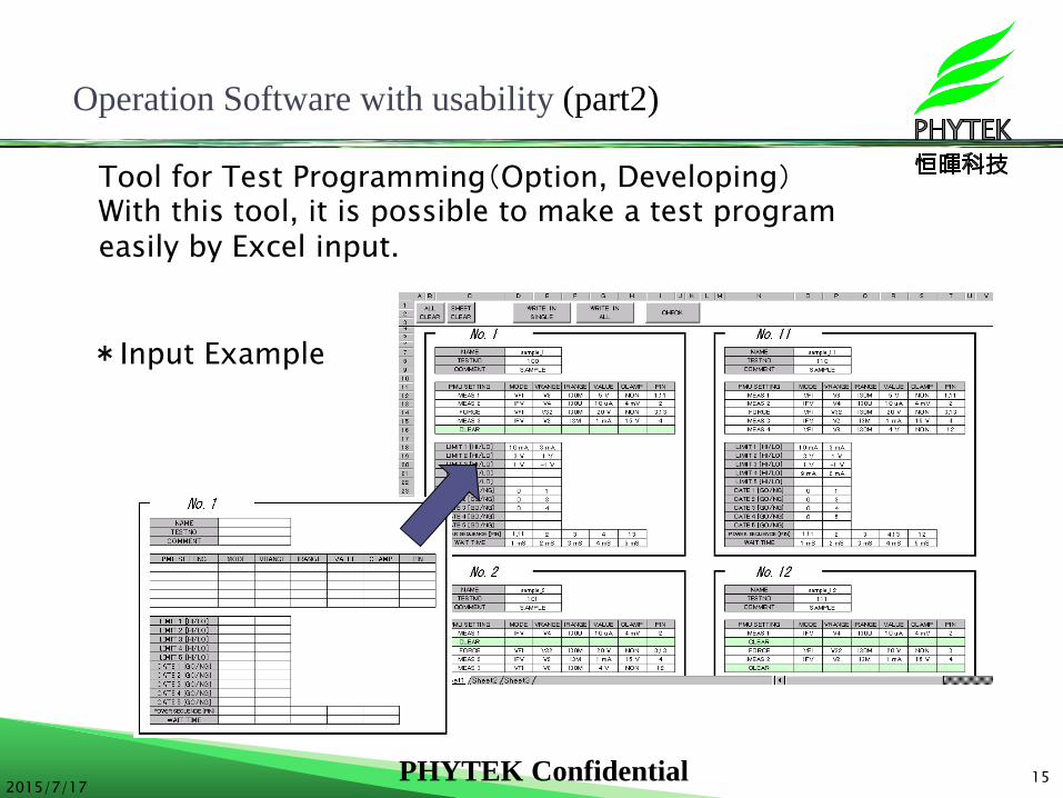
Operation Software with usability (part2)
Tool for Test Programming(Option, Developing) With this tool, it is possible to make a test program easily by Excel input.
*Input Example
2015/7/17 16 PHYTEK Confidential
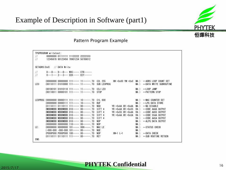
TPGPROGRAM writetest; // 00000000 01111111 11122222 22222333 // 12345678 90123456 78901234 56789012
SETADRS(0x0) // DATA Write
// D---D--- D---D--- WOC----- CTB------ // 0---1--- 2---3--- EEK----- EEY------ (00000000 00000000 111----- 11------,T0 C2L 255 XM:=0x00 YM:=0x0 MA ) ←ADRS LOOP COUNT SET LE0: (00110111 01010000 111----- 11------,T0 SUB LE0PROG MA ) ←DATA WRITE SUBROUTINE
(00100101 01010110 111----- 11------,T0 C2J LE0 MA ) ←LOOP JUMP (00110011 00000101 111----- 11------,T0 STOP MA ) ←PATTERN STOP
LE0PROG:(00000000 00000111 111----- 10------,T0 C1L 600 MA ) ←MAC COUNTER SET (00000000 00000111 111----- 10------,T0 BUF MA ) ←LPG DATA STORE (01110111 01110111 111----- 00------,T0 NGD YR:=0xAA XR:=0xAA MA ) ←NG DISABLE (MBBBMBBB MBBBMBBB 010----- 00------,T0 SIFT 4 YR:=0xAA XR:=0x55 RA ) ←CODE AAAA OUTPUT (MBBBMBBB MBBBMBBB 010----- 00------,T0 SIFT 4 YR:=0x55 XR:=0xAA RA ) ←CODE AA55 OUTPUT (MBBBMBBB MBBBMBBB 010----- 00------,T0 SIFT 4 YR:=0xAA XR:=0x5A RA ) ←CODE 55AA OUTPUT (MBBBMBBB MBBBMBBB 010----- 00------,T0 SIFT 4 RA ) ←CODE AA5A OUTPUT (MBBBMBBB MBBBMBBB 010----- 00------,T0 NOP MA ) ←ALPG DATA OUTPUT (00000000 00000000 110----- 00------,T0 NOP MA ) LE: (H000H000 H000H000 101----- 00H-----,T1 MAC LE MA ) ←STATUS CHECK (-000-000 -000-000 101----- 00------,T0 NGE MA ) (P000P000 P000P000 100----- 00------,T0 NOP XM+1 L+1 MA ) ←DATA CHECK (01110111 01110111 111----- 00------,T0 RET MA ) ←SUB ROUTINE RETUEN END.
Example of Description in Software (part1)
Pattern Program Example

2015/7/17 17 PHYTEK Confidential
Example of Description in Software (part2)
Pattern Program Format
LABEL:(11001LLH 0011HLHL 1001----, T1 M/C OPERAND XM+1 L+1 MA DAI)
ALPG Addressing Control
Micro Instruction
Timing Select
IO Pin LPG Data
ALPG Data Invert
ALPG Addressing Select
T0~T15 PIN1,2,3,..
0, 1
L,H
D,U
-,=
B,F
Z
M/B
M/C
M/R
R/C
XM/XB
XM/XC
XM/XR
XR/XC
YM/YB
YM/YC
YM/YR
YR/YC
NOP
JMP
SUB
RET
C1L
C2L
C1J
C2J
C3L
REP
SIFT
STOP
CFJ1
CFJ2
MAC
CFC
C3J
CFR1
CFR2
NGD
NGE
LPF0-7
UCSTAR
T
UCSTOP
M:=B
B:=M
XM:=XB
XB:=XM
YM:=YB
YB:=YM
M±
R±
XM±
XR±
YM±
YR±
L±
M:=
B:=
R:=
XM:=
YM:=
XB:=
YB:=
XR:=
YR:=
MA
MI
BA
RA
XMA
XMI
XBA
XRA
YMA
YMI
YBA
YRA
DAI
Label: Pattern Code Timing Micro Instruction Operand ALPG ALPG ALPG at driver Select Control Output Select Data Invert


2015/7/17 19 PHYTEK Confidential