physical design challenges and innovations to meet · pdf filephysical design challenges and...
TRANSCRIPT

© 2017 ISPD 1 ISPD 2017 ISPD 2017
Physical Design Challenges and Innovations
to Meet
Power, Speed, and Area Scaling Trend
LC LU
TSMC
TSMC Fellow/Senior Director, R&D

© 2017 ISPD 2 ISPD 2017
Chip and System Integration Trends
for Better PPA & System Performance
SYSTEM
INTEGRATION
System performance/
Bandwidth
Application-specific
Process technology +
Design Solutions
3D
Mobile
High
Performance
Computing
Automotive
IoT
Platform Solutions
Better performance
Better Power
Better form factor
3D Packaging (WLP, WoW)
3D Stacking (BSI, Monolithic MEMS)
3D Transistors (FinFET, GAA-NWT)
SoC
Voice
Video MP
3
Camera
CP
U
Storage
Multiple
Chips
on PCB
2D

© 2017 ISPD 3 ISPD 2017 ISPD 2017
Application-Optimized Design Platforms
Area, Performance and Power
Speed
Power
Functional Safety
Standard Compliance
Automotive
IoT
Speed &
Memory Bandwidth
Ultra-Low Power
Mobile
High-
Performance
Computing

© 2017 ISPD 4 ISPD 2017
Semiconductor Trend
Area: process primary dimension scaling slows down
Very challenging to continue Moore’s law economically
Process and design co-optimization to provide enough area
scaling
Performance: dimension scaling grows metal and via
resistance exponentially
Fully automatic and smart via pillar design flow to reduce high
resistance impact
Power: ultra low voltage for ultra low power
Robust design and variation modeling at low voltages
Heterogeneous integration
Low cost and high system performance 3D packaging
High physical design complexity
Machine learning to be applied to physical design
© 2017 ISPD 5 ISPD 2017
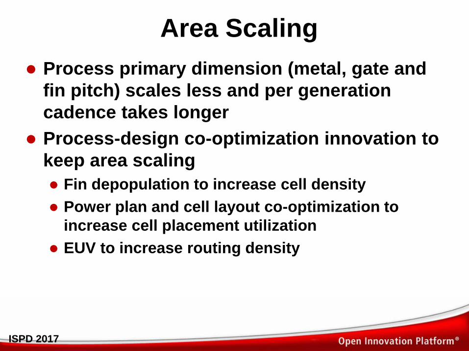
Area Scaling
Process primary dimension (metal, gate and
fin pitch) scales less and per generation
cadence takes longer
Process-design co-optimization innovation to
keep area scaling
Fin depopulation to increase cell density
Power plan and cell layout co-optimization to
increase cell placement utilization
EUV to increase routing density

© 2017 ISPD 6 ISPD 2017 ISPD 2017
Fin Depopulation can Increase Density and Reduce Process Dimension Scaling Pressure
4-fin cell 3-fin cell 2-fin cell

© 2017 ISPD 7 ISPD 2017 ISPD 2017
Fin Depopulation can Increase
Speed and Power Efficiency
Higher fins have highest speed
Fewer fins have highest speed@same power and
lowest power@same speed

© 2017 ISPD 8 ISPD 2017 ISPD 2017
Fin Depopulation Impact on
Logic Density and Cell Utilization
16nm
3~4 fins
10nm
3 fins
7nm
2 fins
70%
75%
80% 1.0
2.0
3.0
Cell
Utilization
Logic
Density
© 2017 ISPD 9 ISPD 2017 ISPD 2017
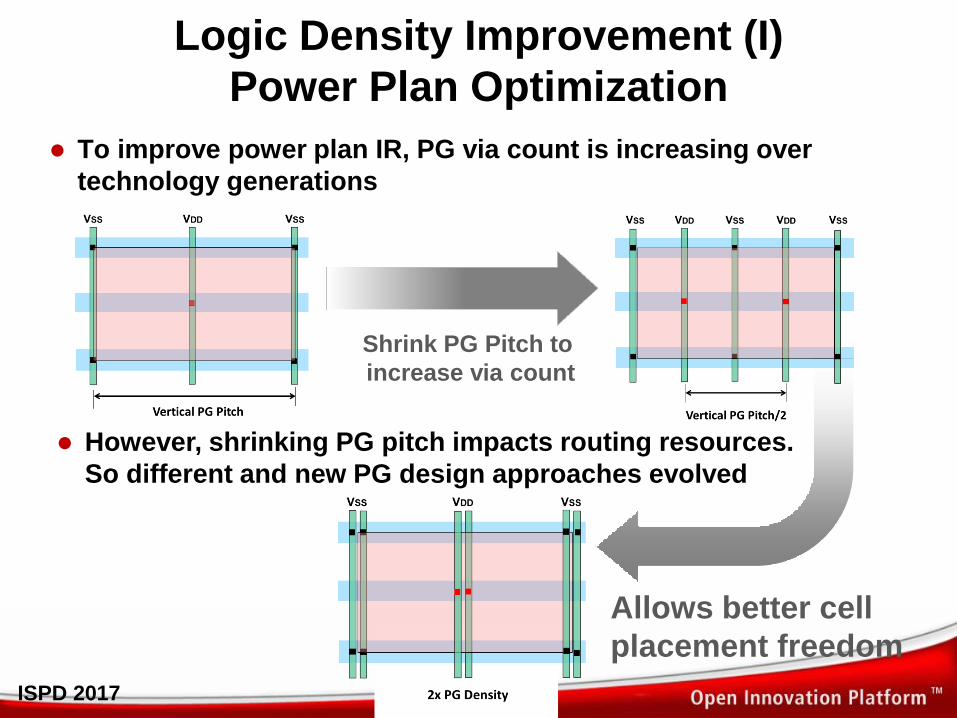
Logic Density Improvement (I)
Power Plan Optimization
To improve power plan IR, PG via count is increasing over
technology generations
Shrink PG Pitch to
increase via count
However, shrinking PG pitch impacts routing resources.
So different and new PG design approaches evolved
Allows better cell
placement freedom

© 2017 ISPD 10 ISPD 2017 ISPD 2017
Uniform M1
Top Down
Bottom Up
Cell re-Design
Big cell design has to be
redesigned to be compatible with
Dual PG architecture
PG and Cell Optimized
Co-Design
Dual M1
PG design has to be friendly to
cell architecture (Uniform Dual)
Logic Density Improvement (II)
Power Plan and Cell Layout Co-optimization

© 2017 ISPD 11 ISPD 2017
Power strap:
Less cells placed under PG
Power stub:
More cells placed under PG
No stagger pin: 5 access points
Stagger pin: 6 access points
Unused
space
Logic Density Improvement (III)
Power Plan and Cell Layout Push to Limit

© 2017 ISPD 12 ISPD 2017 ISPD 2017
Hole type DSA,
16 nm half pitch
Line/Space DSA,
12 nm half pitch
Inverse
Litho.
Directed Self-
Assembly
NXE3300 EUV
Single
Patterning
EUV Multiple
patterning
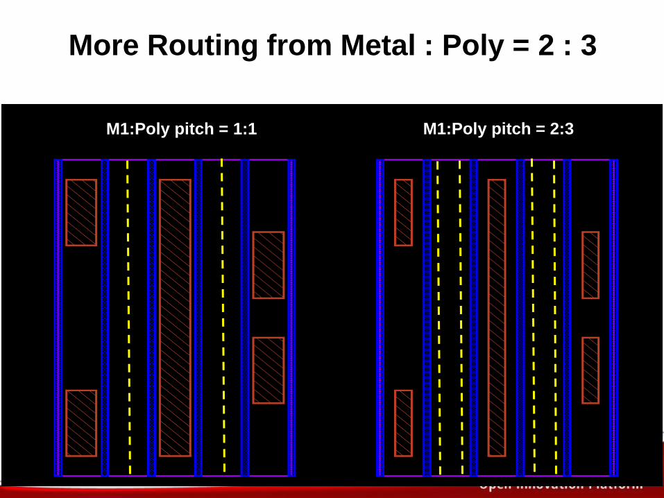
Logic Density Improvement (IV)
EUV to Increase Routing Density

© 2017 ISPD 13 ISPD 2017 ISPD 2017
EUV Metal
Metal : Poly pitch = 2 : 3
More Metal resources for logic density improvement
2 library sets are needed for two metal offset.
Metal:Poly = 1:1 Metal:Poly = 2:3

© 2017 ISPD 14 ISPD 2017 ISPD 2017
ND2D1
M1:PO pitch = 1:1
ND2D1
M1:PO pitch = 2:3
Less Coupling from Metal : Poly = 2 : 3
© 2017 ISPD 15 ISPD 2017 ISPD 2017
M1:Poly pitch = 1:1 M1:Poly pitch = 2:3
More Routing from Metal : Poly = 2 : 3
© 2017 ISPD 16 ISPD 2017 ISPD 2017
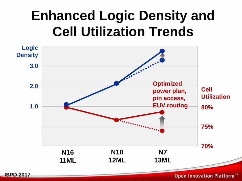
Enhanced Logic Density and
Cell Utilization Trends
N16
11ML
N10
12ML
N7
13ML
70%
75%
80% 1.0
2.0
3.0
Cell
Utilization
Logic
Density
Optimized
power plan,
pin access,
EUV routing
© 2017 ISPD 17 ISPD 2017
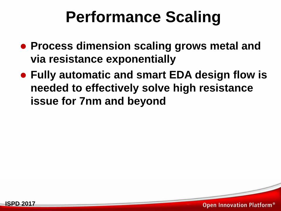
Performance Scaling
Process dimension scaling grows metal and
via resistance exponentially
Fully automatic and smart EDA design flow is
needed to effectively solve high resistance
issue for 7nm and beyond

© 2017 ISPD 18 ISPD 2017 ISPD 2017
0.8
1
1.2
1.4
1.6
1.8
2
0
15
30
45
60
75
40nm 28nm 16nm 7nm 5nm
Mx
C
ap
(vs
. 4
0n
m)
Mx
Re
sis
tan
ce
(vs
. 4
0n
m)
Cross Node Metal RC Scaling
increase ~3X
increase ~3X Mx C
Mx R
© 2017 ISPD 19 ISPD 2017 ISPD 2017
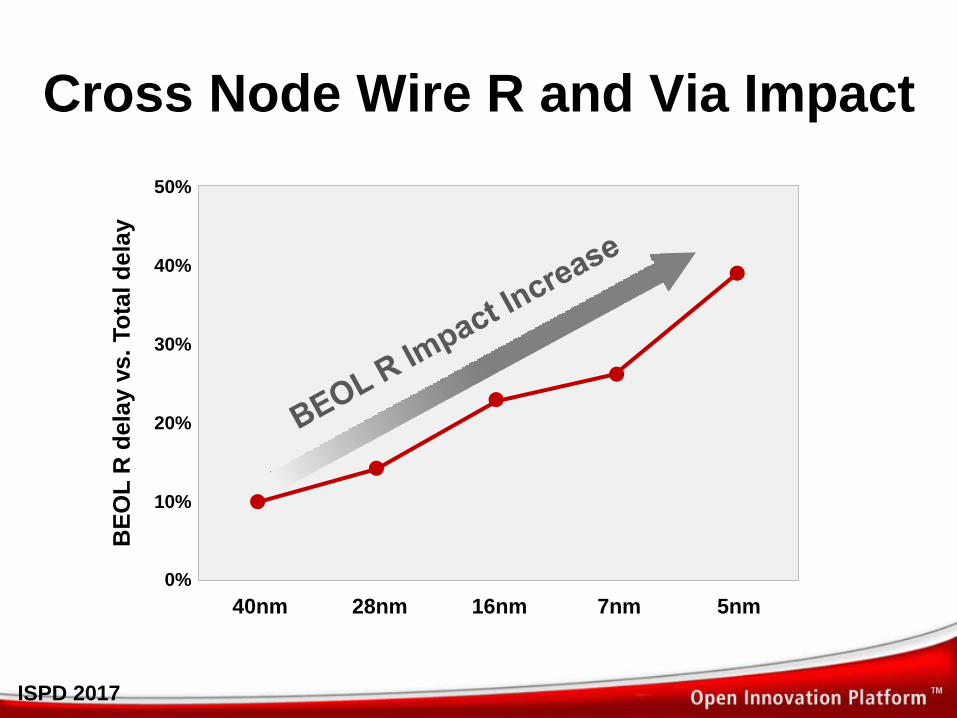
Cross Node Wire R and Via Impact B
EO
L R
de
lay v
s.
To
tal d
ela
y
40nm 28nm 16nm 7nm 5nm
50%
40%
30%
20%
10%
0%
© 2017 ISPD 20 ISPD 2017 ISPD 2017
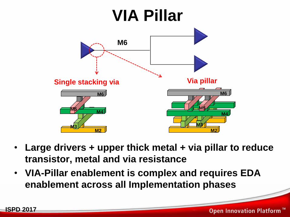
VIA Pillar
• Large drivers + upper thick metal + via pillar to reduce
transistor, metal and via resistance
• VIA-Pillar enablement is complex and requires EDA
enablement across all Implementation phases
M2
M4
M5
M6
M3
M2
M4 M5
M6
M3
M6
Via pillar Single stacking via

© 2017 ISPD 21 ISPD 2017 ISPD 2017
Via Pillar Insertion
Metal R Source Via R
55.43X 1X
Metal R Source Via R
13.23X 3.29X
Metal R Source Via R
13.23X 1X
Implies layer promotion for better wire resistance
Effectively reduces source Via resistance
Connection through DPT layer: DPT wire resistance dominates
Layer promotion to non-DPT layer: Source Via resistance increases
Via pillar: Best combination of metal and source Via resistance
Std. cell Double Patterning
Technology (DTP) Layer
Non-Double Patterning
Technology (DTP) Layer
Std.
cell Wire
(20μm)

© 2017 ISPD 22 ISPD 2017 ISPD 2017
Cross Node Wire R and Via Impact B
EO
L R
de
lay v
s.
To
tal d
ela
y
40nm 28nm 16nm 7nm 5nm
with Via Pillar
50%
40%
30%
20%
10%
0%
© 2017 ISPD 23 ISPD 2017 ISPD 2017
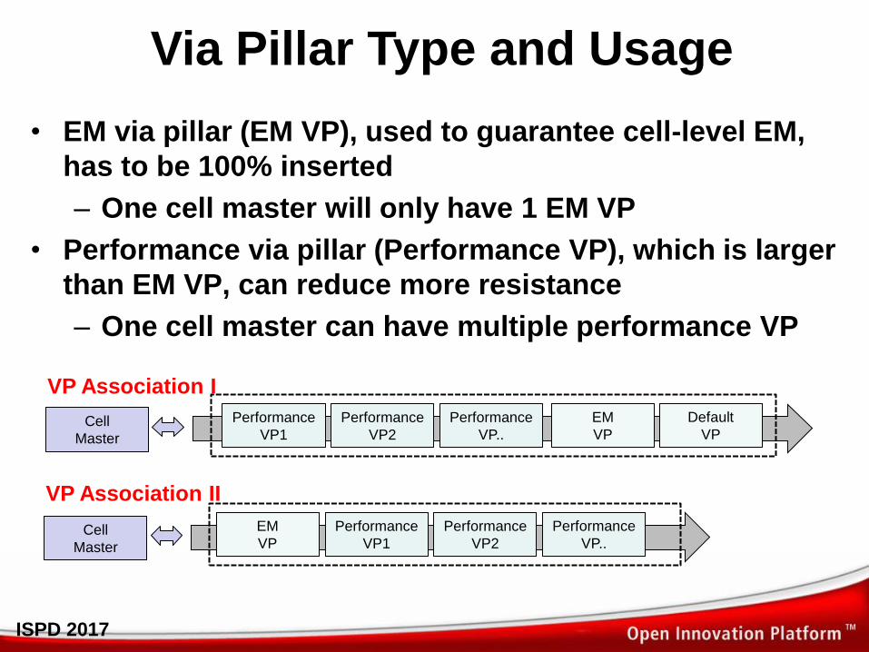
• EM via pillar (EM VP), used to guarantee cell-level EM,
has to be 100% inserted
– One cell master will only have 1 EM VP
• Performance via pillar (Performance VP), which is larger
than EM VP, can reduce more resistance
– One cell master can have multiple performance VP
Cell
Master
VP Association I
EM
VP
Default
VP
Performance
VP1
Performance
VP2
Performance
VP..
Cell
Master
VP Association II
EM
VP
Performance
VP1
Performance
VP2
Performance
VP..
Via Pillar Type and Usage

© 2017 ISPD 24 ISPD 2017 ISPD 2017
Via Pillar Automatic Design Flow
Floorplan
Placement
CTS
Routing/Opt.
Design Kits •VIA pillar (VP) definition, association
• VP aware placement
• Automatic NDR
• VP insertion and verification
• CTS with VP
• VP optimization
• DEF out option

© 2017 ISPD 25 ISPD 2017
Voltage and Power Scaling
Low voltage design reduces power effectively
Low voltage design challenges
Functionality robustness
Accurate variation modeling
© 2017 ISPD 26 ISPD 2017 ISPD 2017
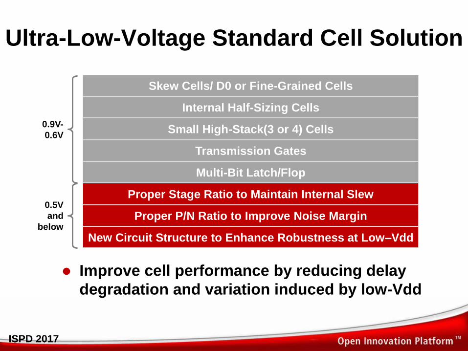
Ultra-Low-Voltage Standard Cell Solution
Skew Cells/ D0 or Fine-Grained Cells
Internal Half-Sizing Cells
Small High-Stack(3 or 4) Cells
Transmission Gates
Multi-Bit Latch/Flop
Proper Stage Ratio to Maintain Internal Slew
Proper P/N Ratio to Improve Noise Margin
New Circuit Structure to Enhance Robustness at Low–Vdd
0.9V-
0.6V
0.5V
and
below
Improve cell performance by reducing delay
degradation and variation induced by low-Vdd

© 2017 ISPD 27 ISPD 2017 ISPD 2017
Flop Low Voltage Design Robustness
• High sigma design checks are required to ensure
robust operation at low operating voltage
• For write operation, forward path (red) must be
stronger than feedback path (blue)
clk_b
clk
QN
D
SI
clk
clk_b clk
clk_b
clk
clk_b
Reset
Reset
Reset
Reset

© 2017 ISPD 28 ISPD 2017 ISPD 2017
Delay Variation Increases at
Lower VDD
0
0.2
0.4
0.6
0.8
1
1.2
1.4
1.6
1.8
2
Lo
g o
f s
ca
led
de
lay s
tan
da
rd
de
via
tio
n
VDD
Delay variation increases
exponentially as VDD decreases
◄ Non-Gaussian
at low voltage
Gaussian ►
at regular voltage

© 2017 ISPD 29 ISPD 2017 ISPD 2017
Abnormal Hold-Time Caused by
Low-Vdd Non-Gaussian Behavior
Regular VDD
Low VDD
Flop Hold Constraint Behavior
Hold time
Ou
tpu
t

© 2017 ISPD 30 ISPD 2017 ISPD 2017
Solutions for Low-Vdd Variations (I)
Methodology improvement
– Timing values are models by both “mean” and
“early/late distribution”
– Implement the new models in timing characterization
and STA tools Original distribution
(Non-Gaussian with
long right tail)
“Early” distribution
to cover short tail “Late” distribution
to cover long tail

© 2017 ISPD 31 ISPD 2017 ISPD 2017
Solutions for Low-Vdd Variations (II)
By using new timing model and advanced statistical
OCV method, we achieve more accurate STA results
compared to Monte-Carlo simulations
Optimistic
Sla
ck
Path ID
SPICE Monte Carlo
Simple OCV
Advanced Statistical OCV

© 2017 ISPD 32 ISPD 2017
Heterogeneous Integration
Low cost and high system performance
InFO and CoWoS integration
Integrated EDA design flow for package and
chips
© 2017 ISPD 33 ISPD 2017 ISPD 2017
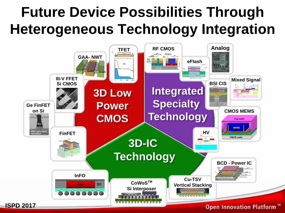
Future Device Possibilities Through
Heterogeneous Technology Integration
3D Low
Power
CMOS
Integrated
Specialty
Technology
3D-IC
Technology
InFO
CoWoSTM
Si Interposer
Cu-TSV
Vertical Stacking
BCD - Power IC
HV
Mixed Signal BSI CIS
CMOS MEMS
Analog
eFlash
RF CMOS TFET
Source Gate Drain
III-V FFET Si CMOS
Ge FinFET
on Si
FinFET
GAA- NWT
© 2017 ISPD 34 ISPD 2017
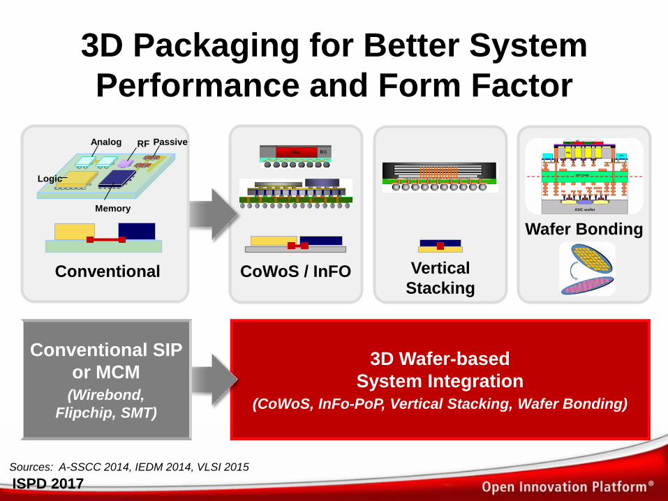
3D Packaging for Better System
Performance and Form Factor
Sources: A-SSCC 2014, IEDM 2014, VLSI 2015
3D Wafer-based
System Integration (CoWoS, InFo-PoP, Vertical Stacking, Wafer Bonding)
Vertical
Stacking CoWoS / InFO
Conventional SIP
or MCM (Wirebond,
Flipchip, SMT)
Conventional
Analog
Logic
RF Passive
Memory
Wafer Bonding
© 2017 ISPD 35 ISPD 2017
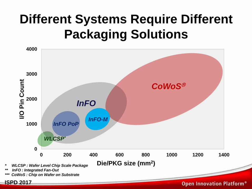
* WLCSP : Wafer Level Chip Scale Package
** InFO : Integrated Fan-Out
*** CoWoS : Chip on Wafer on Substrate
Different Systems Require Different
Packaging Solutions
0
1000
2000
3000
4000
0 200 400 600 800 1000 1200 1400
I/O
Pin
Co
un
t
Die/PKG size (mm2)
CoWoS
WLCSP*
InFO
InFO PoP InFO-M

© 2017 ISPD 36 ISPD 2017
0
1000
2000
3000
4000
0 200 400 600 800 1000 1200 1400
I/O
Pin
Co
un
t
Die/PKG size (mm2)
CoWoS
InFO
InFO PoP InFO-M
Wafer-Level Packaging Technologies:
Integrated Fan-Out (InFO)
InFO PoP InFO-M
InFO
Logic
InFO
DRAM
Logic
InFO-PoP
Through-
InFO–Via
(TIV)
Memory Logic
InFO-M (Multi-chip)
Multi-chips integration
Smallest form-factor
Cost competitive
WLCSP*

© 2017 ISPD 37 ISPD 2017
Wafer-Level Packaging Technologies:
Chip-on-Wafer-on-Substrate (CoWoS)
0
1000
2000
3000
4000
0 200 400 600 800 1000 1200 1400
I/O
Pin
Co
un
t
Die/PKG size (mm2)
CoWoS
InFO
InFO PoP InFO-M
CoWoS
High bandwidth memory
integration for high-performance
computing
WLCSP*
Homogeneous
partition
High-performance
heterogeneous partitioning

© 2017 ISPD 38 ISPD 2017 ISPD 2017
DRAM
Silicon
Insulator1
Insulator2
Core
Insulator4
L1
L2
L3
L4
Insulator5 L5
L6
SR
SR
Molding
Compounds
TMV
250μm
Advanced Packaging Co-Design – SoC + InFO + IPD (Integrated Passive Device)
590μm
InFO-PoP FC-PoP
Thermal
dissipation
improved by 12%
Voltage droop
reduced by 5~10%
Thickness
reduced by 57%
Eye width
improved by >12%
2
1
3
4
Silicon
PM1
PM2
PM3
PM4
B-S pad
RDL0
RDL1
RDL2
RDL3
F-S pad
Molding
Compounds
DRAM
IPD
Rja (15.4 oC/W) Rja (17.2
oC/W)
Eye Opening:
0.785 UI
Eye Opening:
0.663 UI
InFO-PoP W/I IPD
FC-PoP W/O IPD

© 2017 ISPD 39 ISPD 2017
InFO Design Solutions
(InFO Only)
InFO Layout
Creation
InFO DRC/LVS
InFO RC
Extraction
RLCK Extraction < 4GHz RC/RLCK Extraction for STA, IR,
SEM, & PI Analysis
S-parameter Extraction 4GHz – 10GHz S-parameters Extraction
for SI/PI, & EMI analysis
CDL Netlist Auto-Export
PKG Layout InFO
LVS
InFO GDS
InFO CDL
Netlist
PKG Layout In-design DRC
© 2017 ISPD 40 ISPD 2017
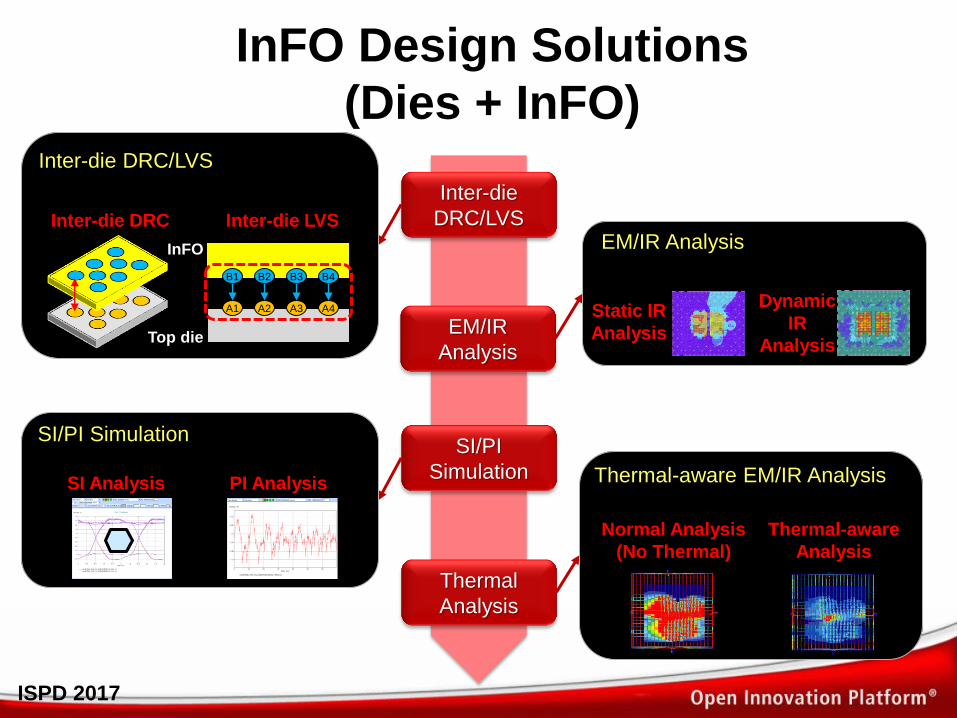
InFO Design Solutions
(Dies + InFO)
Inter-die
DRC/LVS
SI/PI
Simulation
Thermal
Analysis
SI/PI Simulation
SI Analysis PI Analysis
EM/IR
Analysis
EM/IR Analysis
Static IR
Analysis
Dynamic
IR
Analysis
Thermal-aware EM/IR Analysis
Normal Analysis
(No Thermal)
Thermal-aware
Analysis
Inter-die DRC/LVS
InFO
Top die
Inter-die DRC
B1 B2 B3 B4
A1 A2 A3 A4
Inter-die LVS
© 2017 ISPD 41 ISPD 2017
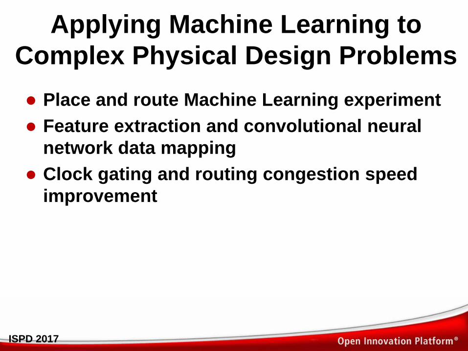
Applying Machine Learning to
Complex Physical Design Problems
Place and route Machine Learning experiment
Feature extraction and convolutional neural
network data mapping
Clock gating and routing congestion speed
improvement
© 2017 ISPD 42 ISPD 2017 ISPD 2017
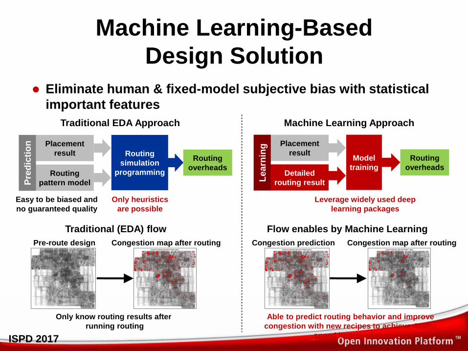
Machine Learning-Based
Design Solution
Eliminate human & fixed-model subjective bias with statistical
important features
Placement
result
Detailed
routing result
Model
training
Le
arn
ing
Routing
overheads
Machine Learning Approach
Leverage widely used deep
learning packages
Placement
result
Routing
pattern model
Routing
simulation
programming
Pre
dic
tio
n
Routing
overheads
Easy to be biased and
no guaranteed quality
Only heuristics
are possible
Traditional EDA Approach
Flow enables by Machine Learning
Able to predict routing behavior and improve
congestion with new recipes to achieve 40Mhz
speed improvement
Congestion prediction Congestion map after routing
Traditional (EDA) flow
Only know routing results after
running routing
Pre-route design Congestion map after routing
© 2017 ISPD 43 ISPD 2017
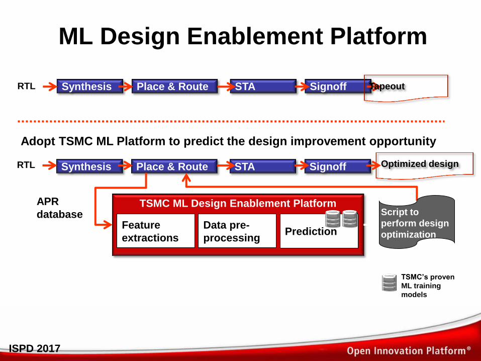
ML Design Enablement Platform
Synthesis Place & Route STA Signoff RTL Tapeout
TSMC ML Design Enablement Platform
Feature
extractions
Data pre-
processing
APR
database
Optimized design
Prediction
Synthesis Place & Route STA Signoff RTL
TSMC’s proven
ML training
models
Adopt TSMC ML Platform to predict the design improvement opportunity
Script to
perform design
optimization

© 2017 ISPD 44 ISPD 2017
ML Design Enablement Platform
TSMC ML Design Enablement Platform
Feature
extractions
Data pre-
processing
APR database
for new
learning
Optimized design
Training
Synthesis Place & Route STA Signoff RTL
TSMC’s
models
Adopt TSMC ML Platform to train design and build new models
Model Mgmt.
Prediction
Customer’s
models
Script to
perform design
optimization
Synthesis Place & Route STA Signoff RTL Tapeout
© 2017 ISPD 45 ISPD 2017 ISPD 2017
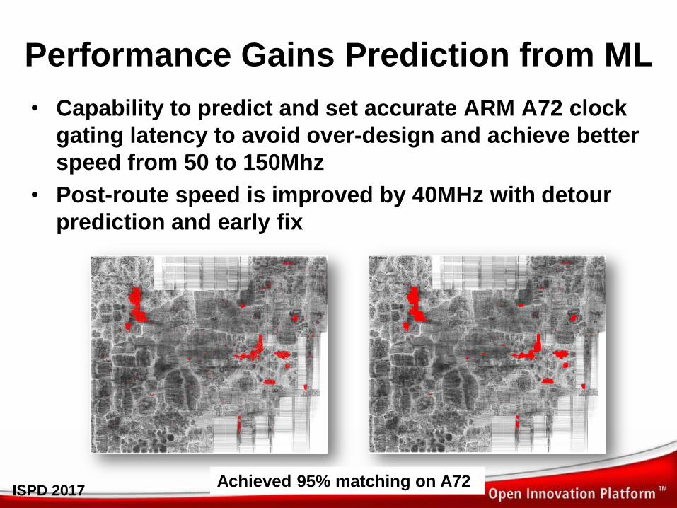
Performance Gains Prediction from ML
• Capability to predict and set accurate ARM A72 clock
gating latency to avoid over-design and achieve better
speed from 50 to 150Mhz
• Post-route speed is improved by 40MHz with detour
prediction and early fix
Real post-route detours Predicted detours
Achieved 95% matching on A72

© 2017 ISPD 46 ISPD 2017 ISPD 2017
Conclusion
Five semiconductor industry trends, issues and
solutions are discussed: area, performance and
power scaling, heterogeneous 3D integration
and Machine Learning
Physical design and EDA play even more critical
roles to extend Moore’s law and to enable highly
integrated complex 3D SOC chips