photonic-electronic ic design and implementation … based on dispersive models and actual layout...
TRANSCRIPT

take control of your photonics design flow
Photonic-Electronic IC design and implementation
Pieter Dumon
27/09/2016

2
Giving photonic IC designers“”the same power as electronic IC designers.
Make it possible to manage design complexity
Large-scale routing O+E co-design Technologies
Layout and verification Very custom design Optical circuit design

Layout driven design flow
3
Handle layout complexity
Intuitive, visual
Drag and drop
Photonics + Electronics
Parametric + hierarchical

IPKISS.eda : Drag and Drop Parametric Cells (Pcells) in L-Edit
4
Drag IPKISS Pcellsinto your design
Easy floorplanning
Adjust PCell parameters

5
Draw connections Generate Waveguides
Circuit definition and layout in L-Edit
Drag and drop PCells

Photonic + Electronic hierarchical design
6
Electro-opticcomponents
Grating coupler I/O
Electrical Pads

Process Design Kit based design
7
• Imec ISIPP50G (SOI)• IME and CMC-IME (SOI)• IHP (SOI + BiCMOS)• Imec BioPIX (SiN)
Idea Design Implementation FabTechnology
Rules
Componentlibrary
Luceda supported foundry technologies

Design Rule Checking
8
Calibre
L-EditLaunch Calibrefrom L-Edit
Inspect DRCerrors directly
in L-Edit

Functional Verification
9
Circuit simulator (compact models)
Frequency and time domain
Incorporate layout effects (discretization)
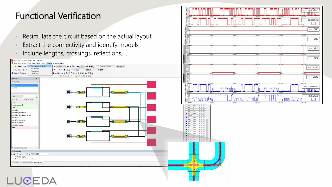
Functional Verification
Resimulate the circuit based on the actual layout
Extract the connectivity and identify models
Include lengths, crossings, reflections, …

11
Giving photonic IC designers“”the same power as electronic IC designers.
Make it possible to manage design complexity
Large-scale routing O+E co-design Technologies
Layout and verification Very custom design Optical circuit design

12
Challenges: typical photonics design flow
Flexibility required
Specify own models and algorithms
Data processing
Integrate on solvers/solutions
Very custom design
Component CAD

Luceda design flow: Graphical UI + scripting
13
IPKISS python script
L-Edit
Componentlibrary

Luceda design flow: Graphical UI + scripting
14
IPKISS python script
L-Edit
Componentlibrary
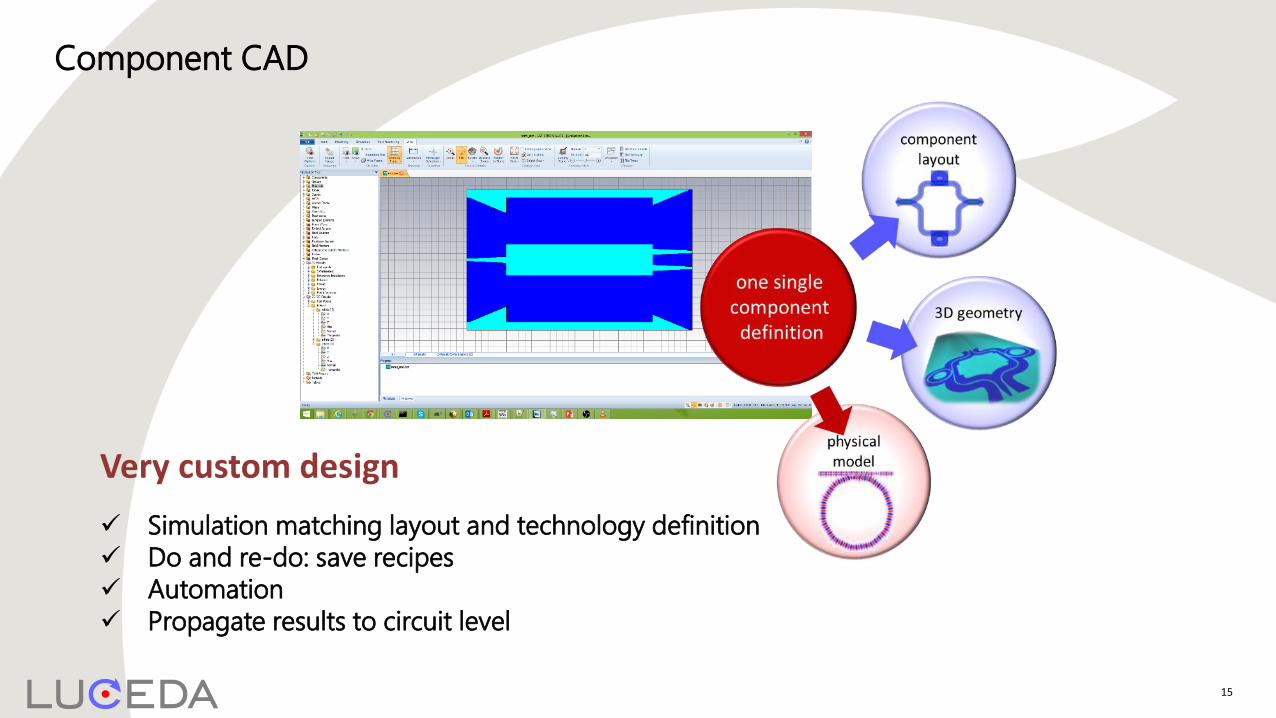
Component CAD
15
Simulation matching layout and technology definition
Do and re-do: save recipes
Automation
Propagate results to circuit level
Very custom design
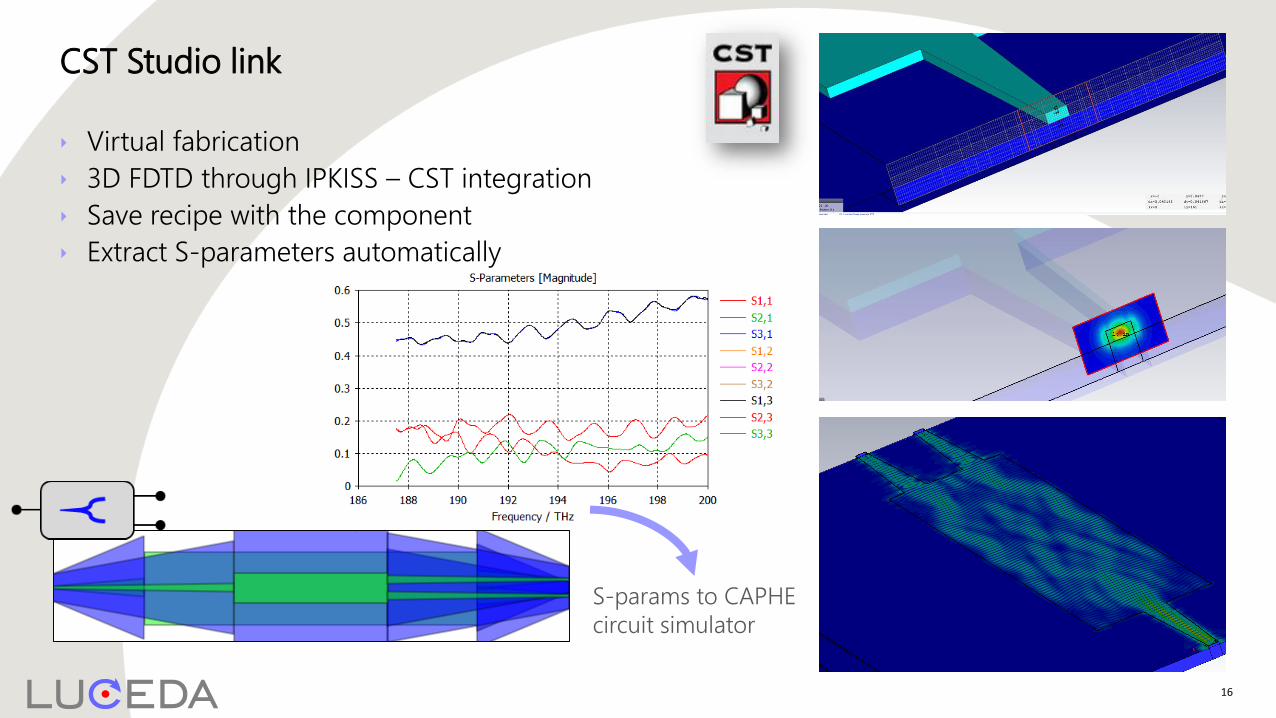
CST Studio link
Virtual fabrication
3D FDTD through IPKISS – CST integration
Save recipe with the component
Extract S-parameters automatically
16
S-params to CAPHE
circuit simulator

IPKISS Filter design tools
AWG, Echelle, MZI lattice filters, Rings, …
Design routines
Simulation based on dispersive models and actual layout
Access to all individual filter parameters
17
layout
field simulation

18
Giving photonic IC designers“”the same power as electronic IC designers.
Make it possible to manage design complexity
Large-scale routing O+E co-design Technologies
Layout and verification Very custom design Optical circuit design

Managing routing complexity
19
Optical and electrical
Start from schematic
Re-use electrical router
Schematic
SDL
Auto routeS-Edit
IPKISS.eda on L-Edit
IPKISS.eda on L-Edit

Managing routing complexity
20
IPKISS.eda on L-Edit
Optical pin-out > 100
Electrical pin-out > 50

Manage complexity: optical and electrical simulation
21
S-Edit schematic
Waveform exchange T-Spice – IPKISS (Caphe)
TSpice IPKISS (Caphe)

Manage complexity: optical and electrical simulation
22
Simulated time traces
Waveform exchange T-Spice – IPKISS (Caphe)

23
High flexibility Easy customization
Fast implementation of fab-specific IPKISS-based photonic Process Design Kitson circuit and layout design levels.
Optical design and layout – manage optical design complexity
VPIcomponentMaker Photonic Circuits Cross-Connect IPKISS

24www.lucedaphotonics.com
Layout DRC & Functional verification EM simulation
Component-centric Intuitive GUI Powerful scripting
Software partners
Giving photonic IC designers“”the same power as electronic IC designers.
Foundry partners