photolithography practical issues illustrations & explanations...az5214e + add step 5000rpm, 30...
TRANSCRIPT

Photolithography Practical Issues –
illustrations & explanations
June 2018 Photolithography issues Dr. B. Yofis

Photolithography process failures – illustrated & explained
2

Flow-chart of the process
flood exposure
Additional steps for the reverse Ph.R
photoresist spin coating
soft bake
alignment & exposure
development
hard bake
General Photolithography Procedure adhesion promoter spin
coating
3
thermal treatment

Photoresist Spin Coating
4

Incomplete sample coating.
not fully covered The surface is not
covered not fully covered
Resist is not at the center
before
the next
photolith
ography The case of the samples
before consequent litho
steps
Resist deficit before spin Resist deficit before spin
The lack of photoresist
The surface is not
smooth
5

small and nonstandard samples must be fully covered by photoresist
Before spinning After spinning
Incomplete sample coating.
Before spin
correct wrong
6

Local non-uniformity of the Photoresist
The defects are easily observed by examining the samples at different angles under the room light
Rays of PhR
Rays of resist
The cause of this effect is small particles or located on the surface of the sample or
transferred by PhR. The second way is most often, and these particles are dry PhR
remnants from the bottle neck or the tip of the pipette. These dry particles are similar
with liquid drops. Second reason for the particles is chipping after scribing or dicing.
1.2µ
Sometimes this effect is observed without the presence of
these particles. Experience allow suggests that even in this
case there is the same reason, but in the second stage of
rotation with increasing speed, the particle is washed away.
The substrate is usable after a
cleaning treatment.
7
The thickness variation of PhR following the particle, measured by a
profilometer

Inertial forces
PhR rays Chipping after dicing Drops of PhR
• The PhR drops are generated around the defects near the edge of the
substrate during the slow spinning step.
• During the fast spinning step, the PhR droplets are spread in the form of the
protruded rays
Solution - polished chamfers at the substrate edges
Local non-uniformity of the resist
8
Centrifugal force
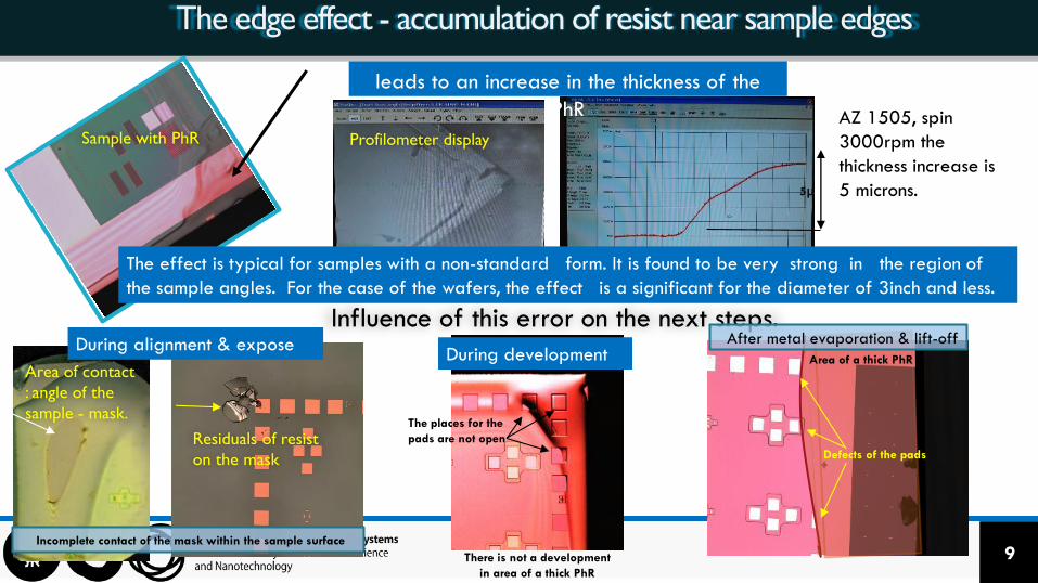
The edge effect - accumulation of resist near sample edges
The effect is typical for samples with a non-standard form. It is found to be very strong in the region of
the sample angles. For the case of the wafers, the effect is a significant for the diameter of 3inch and less.
5µ
AZ 1505, spin
3000rpm the
thickness increase is
5 microns.
Profilometer display Sample with PhR
Influence of this error on the next steps. During alignment & expose
During development After metal evaporation & lift-off
Area of contact
: angle of the
sample - mask.
Residuals of resist
on the mask
There is not a development
in area of a thick PhR
Area of a thick PhR
Defects of the pads
The places for the
pads are not open
9 Incomplete contact of the mask within the sample surface
leads to an increase in the thickness of the
PhR

3000 rpm, 30 sec 5000 rpm, 30 sec 5000 rpm, 30 sec
AZ1505
5000rpm, 30 sec.
AZ 4562
AZ5214E
+ add step
5000rpm,
30 sec.
Use of HMDS
10
Spinner rotation speed
The influence of some basic parameters. on the edge effect

Remove the photoresist from the edge of the sample by expose and development.
This process is recommended to ensure that the mask is pressed against the sample
over the entire area.
resi
st r
em
ova
l fr
om
ang
les
onl
y
Profilometer
Full resist
removal
from the
edges
The conditions for exposure and development are chosen in each case, it is, approximately, possible to recommend: exposure 2-3 min, development 20 - 30 sec.
Thickness of PhR on surface equal
to 0.48µ on angles up to 5µ
480nm
11
11
Using a shield & using shield mask aligner exposure
Using a microscope: no yellow filter & maximum brightness
Using a shield & using shield mask aligner exposure

Soft bake: Hot plate: 95 - 110°C 1 - 2 min ; Oven: 90 - 110°C 5 – 20 min.
Goal of process is:
A removing (evaporation) of a solvent and a formation of PhR layer.
Typical problems of this phase: The duration (temperature) of the heating is not enough for complete removal of the solvent.
10 µ 9µ ≈̴8µ
≈9.5 µ
Good result:
AZ 1518, h = 1,75µ
Soft bake: 110°C, 1 min
Exposer: 4.5 sec.
Development:
35 sec.
The same process with:
Soft bake: 100°C,
45 sec.
Edge of PhR is not sharp,
dimension is decreased.
The increase in exposure
time will not improve the
pattern
Increasing the
development time
leads to distortion of
the pattern and PhR
rising from edge Very typical expansion of the
feature edge - a big angle
slope of the developed PhR
12
Alignment & Exposure Goal of the step:
• Alignment between actual layer and the layer patterned before.
Short description: • The sample and mask are placed within the mask aligner. The movable
chuck with sample moves to achieve the proper alignment between
sample and mask alignment marks.
• After alignment the PhR is exposed to UV light during the exposure
time.
Typical errors leading to failure: • Alignment imperfections –are detected using alignment marks.
• Contact imperfections between mask and sample – non-uniformities
in patterned structures.
13

Alignment between two
lithographic steps
2nd layer marks 1st layer marks
1st step marks Misaligned layers Perfect alignment
Alignment between marks for 3 sequential
lithographic layers
X-shift Y-shift
Alignment & Exposure
3d layer marks
2nd step marks
14

The mask touch to sample is not good enough (or is non uniform, or there is distance)
Angle of the sample
Residuals of
PhR on the
mask
Repetition from page 8
Sample Mask
Sign of distance
is Newton's
Rings
The area of the
photoresist is
broken by pressure
The removing of edge effect is not completed
The area of the
photoresist is
broken by
pressure
15

The mask touch to sample is not good enough (or is non uniform, or there is distance)
(continuation)
Area of photoresist
that interferes to
contact
The photoresist removal
The converting of the figure edges
16

Top view of the revers PhR after development (Illustration for right development)
broken edge shape (occasionally)
particle of PhR
Goal of the step: to remove the soluble part of PhR; create pattern within PhR.
Description: the sample with resist is placed in a vessel (e.g. in Petri dish) with the developer for
the specific time.
Typical errors leading to failure: Time of development is not right.
Development
17

Inverted particle of PhR The particles of PhR after shift Shift of PhR-line
Disconnection of
PhR from substrate
Residuals of
PhR-line
6.49
3.81
side view
(drawing)
Development Overdevelopment or the first exposure (reverse Ph.L.) is not enough (see also page 11)
18

Development
Underdeveloped PhR
Resist residuals area
19