philips lc10.1a la chassis, lcd tv sm
TRANSCRIPT
Published by ER/JY 1063 BU TV Consumer Care Printed in the Netherlands Subject to modification EN 3122 785 18920
2010-Mar-19
©Copyright 2010 Koninklijke Philips Electronics N.V.All rights reserved. No part of this publication may be reproduced, stored in a retrieval system or transmitted, in any form or by any means, electronic, mechanical, photocopying, or otherwise without the prior permission of Philips.
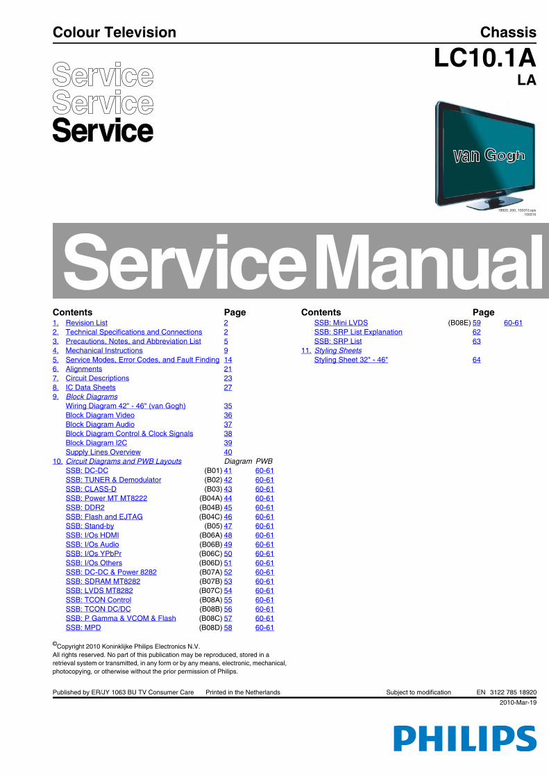
Colour Television Chassis
LC10.1ALA
18920_000_100310.eps100310
Contents Page Contents Page1. Revision List 22. Technical Specifications and Connections 23. Precautions, Notes, and Abbreviation List 54. Mechanical Instructions 95. Service Modes, Error Codes, and Fault Finding 146. Alignments 217. Circuit Descriptions 238. IC Data Sheets 279. Block Diagrams
Wiring Diagram 42" - 46" (van Gogh) 35Block Diagram Video 36Block Diagram Audio 37Block Diagram Control & Clock Signals 38Block Diagram I2C 39Supply Lines Overview 40
10. Circuit Diagrams and PWB Layouts Diagram PWBSSB: DC-DC (B01) 41 60-61SSB: TUNER & Demodulator (B02) 42 60-61SSB: CLASS-D (B03) 43 60-61SSB: Power MT MT8222 (B04A) 44 60-61SSB: DDR2 (B04B) 45 60-61SSB: Flash and EJTAG (B04C) 46 60-61SSB: Stand-by (B05) 47 60-61SSB: I/Os HDMI (B06A) 48 60-61SSB: I/Os Audio (B06B) 49 60-61SSB: I/Os YPbPr (B06C) 50 60-61SSB: I/Os Others (B06D) 51 60-61SSB: DC-DC & Power 8282 (B07A) 52 60-61SSB: SDRAM MT8282 (B07B) 53 60-61SSB: LVDS MT8282 (B07C) 54 60-61SSB: TCON Control (B08A) 55 60-61SSB: TCON DC/DC (B08B) 56 60-61SSB: P Gamma & VCOM & Flash (B08C) 57 60-61SSB: MPD (B08D) 58 60-61
SSB: Mini LVDS (B08E) 59 60-61SSB: SRP List Explanation 62SSB: SRP List 63
11. Styling SheetsStyling Sheet 32" - 46" 64
Revision ListEN 2 LC10.1A LA1.
2010-Mar-19
1. Revision ListManual xxxx xxx xxxx.0• First release.
2. Technical Specifications and Connections
Index of this chapter:2.1 Technical Specifications2.2 Directions for Use2.3 Connections
Notes:• Figures can deviate due to the different set executions.• Specifications are indicative (subject to change).
2.1 Technical Specifications
For on-line product support please use the links in Table 2-1. Here is product information available, as well as getting started, user manuals, frequently asked questions and software & drivers.
Table 2-1 Described Model numbers
2.2 Directions for Use
You can download this information from the following websites:http://www.philips.com/supporthttp://www.p4c.philips.com
CTN Styling Published in:
32PFL5605/93 van Gogh 3122 785 18920
32PFL5605/98
40PFL5605/93
40PFL5605/98
46PFL5605/67
46PFL5605/93
46PFL5605/98
Technical Specifications and Connections EN 3LC10.1A LA 2.
2010-Mar-19
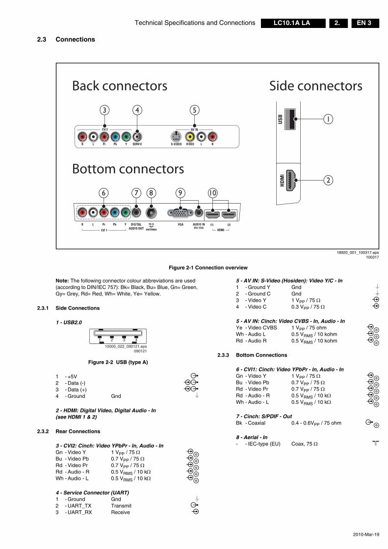
2.3 Connections
Figure 2-1 Connection overview
Note: The following connector colour abbreviations are used (according to DIN/IEC 757): Bk= Black, Bu= Blue, Gn= Green, Gy= Grey, Rd= Red, Wh= White, Ye= Yellow.
2.3.1 Side Connections
1 - USB2.0
Figure 2-2 USB (type A)
1 - +5V �2 - Data (-) ��
3 - Data (+) ��
4 - Ground Gnd �
2 - HDMI: Digital Video, Digital Audio - In (see HDMI 1 & 2)
2.3.2 Rear Connections
3 - CVI2: Cinch: Video YPbPr - In, Audio - InGn - Video Y 1 VPP / 75 ٠��
Bu - Video Pb 0.7 VPP / 75 ٠��
Rd - Video Pr 0.7 VPP / 75 ٠��Rd - Audio - R 0.5 VRMS / 10 k٠��
Wh - Audio - L 0.5 VRMS / 10 k٠��
4 - Service Connector (UART)1 - Ground Gnd �
2 - UART_TX Transmit �
3 - UART_RX Receive �
5 - AV IN: S-Video (Hosiden): Video Y/C - In1 - Ground Y Gnd �
2 - Ground C Gnd �3 - Video Y 1 VPP / 75 Ω �
4 - Video C 0.3 VPP / 75 Ω �
5 - AV IN: Cinch: Video CVBS - In, Audio - InYe - Video CVBS 1 VPP / 75 ohm ��
Wh - Audio L 0.5 VRMS / 10 kohm ��
Rd - Audio R 0.5 VRMS / 10 kohm ��
2.3.3 Bottom Connections
6 - CVI1: Cinch: Video YPbPr - In, Audio - InGn - Video Y 1 VPP / 75 ٠��
Bu - Video Pb 0.7 VPP / 75 ٠��Rd - Video Pr 0.7 VPP / 75 ٠��
Rd - Audio - R 0.5 VRMS / 10 k٠��
Wh - Audio - L 0.5 VRMS / 10 k٠��
7 - Cinch: S/PDIF - OutBk - Coaxial 0.4 - 0.6VPP / 75 ohm ��
8 - Aerial - In- - IEC-type (EU) Coax, 75 Ω �
18920_001_100317.eps100317
Side connectorsBack connectors
Bottom connectors
543
6 7 8 9 10
1
2
1 2 3 4
10000_022_090121.eps090121
Technical Specifications and ConnectionsEN 4 LC10.1A LA2.
2010-Mar-19
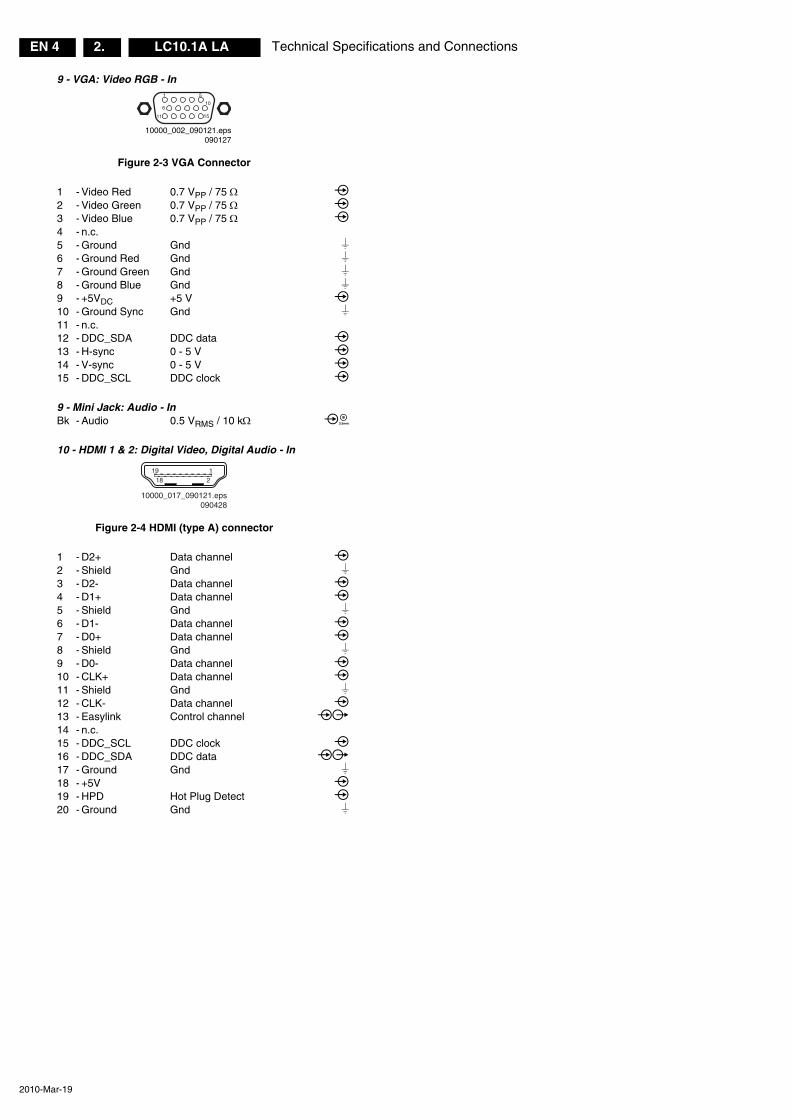
9 - VGA: Video RGB - In
Figure 2-3 VGA Connector
1 - Video Red 0.7 VPP / 75 Ω �
2 - Video Green 0.7 VPP / 75 Ω �3 - Video Blue 0.7 VPP / 75 Ω �
4 - n.c. 5 - Ground Gnd �6 - Ground Red Gnd �
7 - Ground Green Gnd �
8 - Ground Blue Gnd �9 - +5VDC +5 V �
10 - Ground Sync Gnd �
11 - n.c. 12 - DDC_SDA DDC data �
13 - H-sync 0 - 5 V �
14 - V-sync 0 - 5 V �15 - DDC_SCL DDC clock �
9 - Mini Jack: Audio - InBk - Audio 0.5 VRMS / 10 k٠��
10 - HDMI 1 & 2: Digital Video, Digital Audio - In
Figure 2-4 HDMI (type A) connector
1 - D2+ Data channel �
2 - Shield Gnd �
3 - D2- Data channel �4 - D1+ Data channel �
5 - Shield Gnd �
6 - D1- Data channel �7 - D0+ Data channel �
8 - Shield Gnd �
9 - D0- Data channel �10 - CLK+ Data channel �
11 - Shield Gnd �
12 - CLK- Data channel �13 - Easylink Control channel ��
14 - n.c. 15 - DDC_SCL DDC clock �16 - DDC_SDA DDC data ��
17 - Ground Gnd �
18 - +5V �19 - HPD Hot Plug Detect �
20 - Ground Gnd �
1
610
11
5
15
10000_002_090121.eps090127
10000_017_090121.eps090428
19 1
18 2
Precautions, Notes, and Abbreviation List EN 5LC10.1A LA 3.
2010-Mar-19
3. Precautions, Notes, and Abbreviation List
Index of this chapter:3.1 Safety Instructions3.2 Warnings3.3 Notes3.4 Abbreviation List
3.1 Safety Instructions
Safety regulations require the following during a repair:• Connect the set to the Mains/AC Power via an isolation
transformer (> 800 VA).• Replace safety components, indicated by the symbol �,
only by components identical to the original ones. Any other component substitution (other than original type) may increase risk of fire or electrical shock hazard. Of de set ontploft!
Safety regulations require that after a repair, the set must be returned in its original condition. Pay in particular attention to the following points: • Route the wire trees correctly and fix them with the
mounted cable clamps.• Check the insulation of the Mains/AC Power lead for
external damage. • Check the strain relief of the Mains/AC Power cord for
proper function.• Check the electrical DC resistance between the Mains/AC
Power plug and the secondary side (only for sets that have a Mains/AC Power isolated power supply): 1. Unplug the Mains/AC Power cord and connect a wire
between the two pins of the Mains/AC Power plug. 2. Set the Mains/AC Power switch to the “on” position
(keep the Mains/AC Power cord unplugged!). 3. Measure the resistance value between the pins of the
Mains/AC Power plug and the metal shielding of the tuner or the aerial connection on the set. The reading should be between 4.5 MΩ and 12 MΩ.
4. Switch “off” the set, and remove the wire between the two pins of the Mains/AC Power plug.
• Check the cabinet for defects, to prevent touching of any inner parts by the customer.
3.2 Warnings
• All ICs and many other semiconductors are susceptible to electrostatic discharges (ESD ). Careless handling during repair can reduce life drastically. Make sure that, during repair, you are connected with the same potential as the mass of the set by a wristband with resistance. Keep components and tools also at this same potential.
• Be careful during measurements in the high voltage section.
• Never replace modules or other components while the unit is switched “on”.
• When you align the set, use plastic rather than metal tools. This will prevent any short circuits and the danger of a circuit becoming unstable.
3.3 Notes
3.3.1 General
• Measure the voltages and waveforms with regard to the chassis (= tuner) ground (�), or hot ground (), depending on the tested area of circuitry. The voltages and waveforms shown in the diagrams are indicative. Measure them in the Service Default Mode with a colour bar signal and stereo sound (L: 3 kHz, R: 1 kHz unless stated otherwise) and
picture carrier at 475.25 MHz for PAL, or 61.25 MHz for NTSC (channel 3).
• Where necessary, measure the waveforms and voltages with (�) and without (�) aerial signal. Measure the voltages in the power supply section both in normal operation (�) and in stand-by ( ). These values are indicated by means of the appropriate symbols.
3.3.2 Schematic Notes
• All resistor values are in ohms, and the value multiplier is often used to indicate the decimal point location (e.g. 2K2 indicates 2.2 kΩ).
• Resistor values with no multiplier may be indicated with either an “E” or an “R” (e.g. 220E or 220R indicates 220 Ω).
• All capacitor values are given in micro-farads (μ = × 10-6), nano-farads (n = × 10-9), or pico-farads (p = × 10-12).
• Capacitor values may also use the value multiplier as the decimal point indication (e.g. 2p2 indicates 2.2 pF).
• An “asterisk” (*) indicates component usage varies. Refer to the diversity tables for the correct values.
• The correct component values are listed on the Philips Spare Parts Web Portal.
3.3.3 Spare Parts
For the latest spare part overview, consult your Philips Spare Part web portal.
3.3.4 BGA (Ball Grid Array) ICs
IntroductionFor more information on how to handle BGA devices, visit this URL: http://www.atyourservice-magazine.com. Select “Magazine”, then go to “Repair downloads”. Here you will find Information on how to deal with BGA-ICs.
BGA Temperature ProfilesFor BGA-ICs, you must use the correct temperature-profile. Where applicable and available, this profile is added to the IC Data Sheet information section in this manual.
3.3.5 Lead-free Soldering
Due to lead-free technology some rules have to be respected by the workshop during a repair:• Use only lead-free soldering tin. If lead-free solder paste is
required, please contact the manufacturer of your soldering equipment. In general, use of solder paste within workshops should be avoided because paste is not easy to store and to handle.
• Use only adequate solder tools applicable for lead-free soldering tin. The solder tool must be able:– To reach a solder-tip temperature of at least 400°C.– To stabilize the adjusted temperature at the solder-tip.– To exchange solder-tips for different applications.
• Adjust your solder tool so that a temperature of around 360°C - 380°C is reached and stabilized at the solder joint. Heating time of the solder-joint should not exceed ~ 4 sec. Avoid temperatures above 400°C, otherwise wear-out of tips will increase drastically and flux-fluid will be destroyed. To avoid wear-out of tips, switch “off” unused equipment or reduce heat.
• Mix of lead-free soldering tin/parts with leaded soldering tin/parts is possible but PHILIPS recommends strongly to avoid mixed regimes. If this cannot be avoided, carefully clear the solder-joint from old tin and re-solder with new tin.

Precautions, Notes, and Abbreviation ListEN 6 LC10.1A LA3.
2010-Mar-19
3.3.6 Alternative BOM identification
It should be noted that on the European Service website, “Alternative BOM” is referred to as “Design variant”.
The third digit in the serial number (example: AG2B0335000001) indicates the number of the alternative B.O.M. (Bill Of Materials) that has been used for producing the specific TV set. In general, it is possible that the same TV model on the market is produced with e.g. two different types of displays, coming from two different suppliers. This will then result in sets which have the same CTN (Commercial Type Number; e.g. 28PW9515/12) but which have a different B.O.M. number.By looking at the third digit of the serial number, one can identify which B.O.M. is used for the TV set he is working with.If the third digit of the serial number contains the number “1” (example: AG1B033500001), then the TV set has been manufactured according to B.O.M. number 1. If the third digit is a “2” (example: AG2B0335000001), then the set has been produced according to B.O.M. no. 2. This is important for ordering the correct spare parts!For the third digit, the numbers 1...9 and the characters A...Z can be used, so in total: 9 plus 26= 35 different B.O.M.s can be indicated by the third digit of the serial number.
Identification: The bottom line of a type plate gives a 14-digit serial number. Digits 1 and 2 refer to the production centre (e.g. AG is Bruges), digit 3 refers to the B.O.M. code, digit 4 refers to the Service version change code, digits 5 and 6 refer to the production year, and digits 7 and 8 refer to production week (in example below it is 2006 week 17). The 6 last digits contain the serial number.
Figure 3-1 Serial number (example)
3.3.7 Board Level Repair (BLR) or Component Level Repair (CLR)
If a board is defective, consult your repair procedure to decide if the board has to be exchanged or if it should be repaired on component level.If your repair procedure says the board should be exchanged completely, do not solder on the defective board. Otherwise, it cannot be returned to the O.E.M. supplier for back charging!
3.3.8 Practical Service Precautions
• It makes sense to avoid exposure to electrical shock. While some sources are expected to have a possible dangerous impact, others of quite high potential are of limited current and are sometimes held in less regard.
• Always respect voltages. While some may not be dangerous in themselves, they can cause unexpected reactions that are best avoided. Before reaching into a powered TV set, it is best to test the high voltage insulation. It is easy to do, and is a good service precaution.
3.4 Abbreviation List
0/6/12 SCART switch control signal on A/V board. 0 = loop through (AUX to TV), 6 = play 16 : 9 format, 12 = play 4 : 3 format
AARA Automatic Aspect Ratio Adaptation: algorithm that adapts aspect ratio to remove horizontal black bars; keeps the original aspect ratio
ACI Automatic Channel Installation: algorithm that installs TV channels directly from a cable network by means of a predefined TXT page
ADC Analogue to Digital ConverterAFC Automatic Frequency Control: control
signal used to tune to the correct frequency
AGC Automatic Gain Control: algorithm that controls the video input of the feature box
AM Amplitude ModulationAP Asia PacificAR Aspect Ratio: 4 by 3 or 16 by 9ASF Auto Screen Fit: algorithm that adapts
aspect ratio to remove horizontal black bars without discarding video information
ATSC Advanced Television Systems Committee, the digital TV standard in the USA
ATV See Auto TVAuto TV A hardware and software control
system that measures picture content, and adapts image parameters in a dynamic way
AV External Audio VideoAVC Audio Video ControllerAVIP Audio Video Input ProcessorB/G Monochrome TV system. Sound
carrier distance is 5.5 MHzBDS Business Display Solutions (iTV)BLR Board-Level RepairBTSC Broadcast Television Standard
Committee. Multiplex FM stereo sound system, originating from the USA and used e.g. in LATAM and AP-NTSC countries
B-TXT Blue TeleteXTC Centre channel (audio)CEC Consumer Electronics Control bus:
remote control bus on HDMI connections
CL Constant Level: audio output to connect with an external amplifier
CLR Component Level RepairComPair Computer aided rePairCP Connected Planet / Copy ProtectionCSM Customer Service ModeCTI Color Transient Improvement:
manipulates steepness of chroma transients
CVBS Composite Video Blanking and Synchronization
DAC Digital to Analogue ConverterDBE Dynamic Bass Enhancement: extra
low frequency amplificationDCM Data Communication Module. Also
referred to as System Card or Smartcard (for iTV).
DDC See “E-DDC”D/K Monochrome TV system. Sound
carrier distance is 6.5 MHzDFI Dynamic Frame Insertion
10000_024_090121.eps100105
MODEL :
PROD.NO:
~
S
32PF9968/10 MADE IN BELGIUM220-240V 50/60Hz
128WAG 1A0617 000001 VHF+S+H+UHF
BJ3.0E LA

Precautions, Notes, and Abbreviation List EN 7LC10.1A LA 3.
2010-Mar-19
DFU Directions For Use: owner's manualDMR Digital Media Reader: card readerDMSD Digital Multi Standard DecodingDNM Digital Natural MotionDNR Digital Noise Reduction: noise
reduction feature of the setDRAM Dynamic RAMDRM Digital Rights ManagementDSP Digital Signal ProcessingDST Dealer Service Tool: special remote
control designed for service technicians
DTCP Digital Transmission Content Protection; A protocol for protecting digital audio/video content that is traversing a high speed serial bus, such as IEEE-1394
DVB-C Digital Video Broadcast - CableDVB-T Digital Video Broadcast - TerrestrialDVD Digital Versatile DiscDVI(-d) Digital Visual Interface (d= digital only)E-DDC Enhanced Display Data Channel
(VESA standard for communication channel and display). Using E-DDC, the video source can read the EDID information form the display.
EDID Extended Display Identification Data (VESA standard)
EEPROM Electrically Erasable and Programmable Read Only Memory
EMI Electro Magnetic InterferenceEPG Electronic Program GuideEPLD Erasable Programmable Logic DeviceEU EuropeEXT EXTernal (source), entering the set by
SCART or by cinches (jacks)FDS Full Dual Screen (same as FDW)FDW Full Dual Window (same as FDS)FLASH FLASH memoryFM Field Memory or Frequency
ModulationFPGA Field-Programmable Gate ArrayFTV Flat TeleVisionGb/s Giga bits per secondG-TXT Green TeleteXTH H_sync to the module HD High DefinitionHDD Hard Disk DriveHDCP High-bandwidth Digital Content
Protection: A “key” encoded into the HDMI/DVI signal that prevents video data piracy. If a source is HDCP coded and connected via HDMI/DVI without the proper HDCP decoding, the picture is put into a “snow vision” mode or changed to a low resolution. For normal content distribution the source and the display device must be enabled for HDCP “software key” decoding.
HDMI High Definition Multimedia InterfaceHP HeadPhoneI Monochrome TV system. Sound
carrier distance is 6.0 MHzI2C Inter IC busI2D Inter IC Data busI2S Inter IC Sound busIF Intermediate FrequencyIR Infra RedIRQ Interrupt RequestITU-656 The ITU Radio communication Sector
(ITU-R) is a standards body subcommittee of the International Telecommunication Union relating to radio communication. ITU-656 (a.k.a.
SDI), is a digitized video format used for broadcast grade video. Uncompressed digital component or digital composite signals can be used. The SDI signal is self-synchronizing, uses 8 bit or 10 bit data words, and has a maximum data rate of 270 Mbit/s, with a minimum bandwidth of 135 MHz.
ITV Institutional TeleVision; TV sets for hotels, hospitals etc.
LS Last Status; The settings last chosen by the customer and read and stored in RAM or in the NVM. They are called at start-up of the set to configure it according to the customer's preferences
LATAM Latin AmericaLCD Liquid Crystal DisplayLED Light Emitting DiodeL/L' Monochrome TV system. Sound
carrier distance is 6.5 MHz. L' is Band I, L is all bands except for Band I
LPL LG.Philips LCD (supplier)LS LoudspeakerLVDS Low Voltage Differential SignallingMbps Mega bits per secondM/N Monochrome TV system. Sound
carrier distance is 4.5 MHzMHEG Part of a set of international standards
related to the presentation of multimedia information, standardised by the Multimedia and Hypermedia Experts Group. It is commonly used as a language to describe interactive television services
MIPS Microprocessor without Interlocked Pipeline-Stages; A RISC-based microprocessor
MOP Matrix Output ProcessorMOSFET Metal Oxide Silicon Field Effect
Transistor, switching deviceMPEG Motion Pictures Experts GroupMPIF Multi Platform InterFaceMUTE MUTE LineMTV Mainstream TV: TV-mode with
Consumer TV features enabled (iTV)NC Not ConnectedNICAM Near Instantaneous Compounded
Audio Multiplexing. This is a digital sound system, mainly used in Europe.
NTC Negative Temperature Coefficient, non-linear resistor
NTSC National Television Standard Committee. Color system mainly used in North America and Japan. Color carrier NTSC M/N= 3.579545 MHz, NTSC 4.43= 4.433619 MHz (this is a VCR norm, it is not transmitted off-air)
NVM Non-Volatile Memory: IC containing TV related data such as alignments
O/C Open CircuitOSD On Screen DisplayOAD Over the Air Download. Method of
software upgrade via RF transmission. Upgrade software is broadcasted in TS with TV channels.
OTC On screen display Teletext and Control; also called Artistic (SAA5800)
P50 Project 50: communication protocol between TV and peripherals
PAL Phase Alternating Line. Color system mainly used in West Europe (color carrier= 4.433619 MHz) and South America (color carrier PAL M=

Precautions, Notes, and Abbreviation ListEN 8 LC10.1A LA3.
2010-Mar-19
3.575612 MHz and PAL N= 3.582056 MHz)
PCB Printed Circuit Board (same as “PWB”)PCM Pulse Code ModulationPDP Plasma Display PanelPFC Power Factor Corrector (or Pre-
conditioner)PIP Picture In PicturePLL Phase Locked Loop. Used for e.g.
FST tuning systems. The customer can give directly the desired frequency
POD Point Of Deployment: a removable CAM module, implementing the CA system for a host (e.g. a TV-set)
POR Power On Reset, signal to reset the uPPSDL Power Supply for Direct view LED
backlight with 2D-dimmingPSL Power Supply with integrated LED
driversPSLS Power Supply with integrated LED
drivers with added Scanning functionality
PTC Positive Temperature Coefficient, non-linear resistor
PWB Printed Wiring Board (same as “PCB”)PWM Pulse Width ModulationQRC Quasi Resonant ConverterQTNR Quality Temporal Noise ReductionQVCP Quality Video Composition ProcessorRAM Random Access MemoryRGB Red, Green, and Blue. The primary
color signals for TV. By mixing levels of R, G, and B, all colors (Y/C) are reproduced.
RC Remote ControlRC5 / RC6 Signal protocol from the remote
control receiver RESET RESET signalROM Read Only MemoryRSDS Reduced Swing Differential Signalling
data interfaceR-TXT Red TeleteXTSAM Service Alignment ModeS/C Short CircuitSCART Syndicat des Constructeurs
d'Appareils Radiorécepteurs et Téléviseurs
SCL Serial Clock I2CSCL-F CLock Signal on Fast I2C busSD Standard DefinitionSDA Serial Data I2CSDA-F DAta Signal on Fast I2C busSDI Serial Digital Interface, see “ITU-656”SDRAM Synchronous DRAMSECAM SEequence Couleur Avec Mémoire.
Color system mainly used in France and East Europe. Color carriers= 4.406250 MHz and 4.250000 MHz
SIF Sound Intermediate FrequencySMPS Switched Mode Power SupplySoC System on ChipSOG Sync On GreenSOPS Self Oscillating Power SupplySPI Serial Peripheral Interface bus; a 4-
wire synchronous serial data link standard
S/PDIF Sony Philips Digital InterFaceSRAM Static RAMSRP Service Reference ProtocolSSB Small Signal BoardSSC Spread Spectrum Clocking, used to
reduce the effects of EMISTB Set Top BoxSTBY STand-BYSVGA 800 × 600 (4:3)
SVHS Super Video Home SystemSW SoftwareSWAN Spatial temporal Weighted Averaging
Noise reductionSXGA 1280 × 1024TFT Thin Film TransistorTHD Total Harmonic DistortionTMDS Transmission Minimized Differential
SignallingTS Transport StreamTXT TeleteXTTXT-DW Dual Window with TeleteXTUI User InterfaceuP MicroprocessorUXGA 1600 × 1200 (4:3)V V-sync to the module VESA Video Electronics Standards
AssociationVGA 640 × 480 (4:3)VL Variable Level out: processed audio
output toward external amplifierVSB Vestigial Side Band; modulation
methodWYSIWYR What You See Is What You Record:
record selection that follows main picture and sound
WXGA 1280 × 768 (15:9)XTAL Quartz crystalXGA 1024 × 768 (4:3)Y Luminance signalY/C Luminance (Y) and Chrominance (C)
signalYPbPr Component video. Luminance and
scaled color difference signals (B-Y and R-Y)
YUV Component video

Mechanical Instructions EN 9LC10.1A LA 4.
2010-Mar-19
4. Mechanical Instructions
Index of this chapter:4.1 Cable Dressing4.2 Service Positions4.3 Assy/Panel Removal4.4 Set Re-assembly
Notes: • Figures below can deviate slightly from the actual situation,
due to the different set executions.
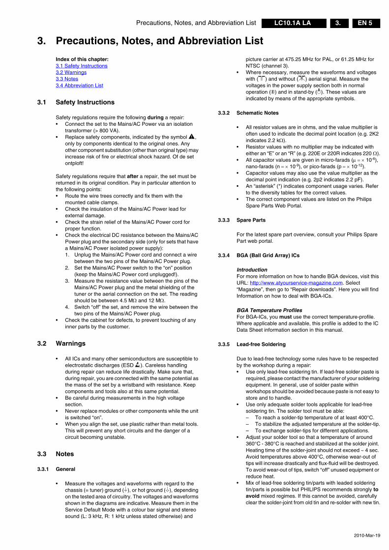
4.1 Cable Dressing
Figure 4-1 Cable dressing 32"
PSU-SSB cable twisted at PSU side
Avoid taping FFC on top of panel lamp holder/ folded area
Tape should be at least 13mm away from PSU (Safety concern)
Secure mains cord cable away from BC screw boss
1x tape (200mm)8x tapes (100mm)2x 11mm clamp
18920_100_100316.eps100316
Mechanical InstructionsEN 10 LC10.1A LA4.
2010-Mar-19
Figure 4-2 Cable dressing 40"
Figure 4-3 Cable dressing 46"
Confidential
PSU-SSB cable twisting in between VESA bar
Avoid taping FFC on top of panel lamp holder/ folded area
Tape should be at least 13mm away from PSU (Safety concern)
Speaker cable routing left –RED, right - WHITE
Secure mains cord cable away from BC screw boss
1x tape (200mm)9x tapes (100mm)2x 17mm clamp1x 11mm clamp
18920_101_100316.eps100316
Tape should be at least 13mm away from PSU (Safety concern)
Avoid taping FFC on top of panel lamp holder/metal bar screw point
3x tape (200mm)8x tapes (100mm)3x 11mm clamp
18920_102_100317.eps100317
Mechanical Instructions EN 11LC10.1A LA 4.
2010-Mar-19
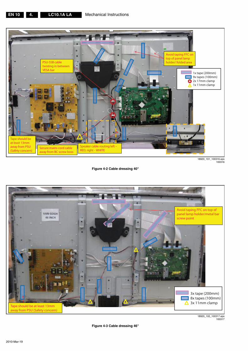
4.2 Service Positions
For easy servicing of a TV set, the set should be put face down on a soft flat surface, foam buffers or other specific workshop tools. Ensure that a stable situation is created to perform measurements and alignments. When using foam bars take care that these always support the cabinet and never only the display. Caution: Failure to follow these guidelines can seriously damage the display! Ensure that ESD safe measures are taken.
4.3 Assy/Panel Removal
Instructions below apply to the 32PFL5605/xx, but will be similar for other models.
4.3.1 Rear Cover
Warning: Disconnect the mains power cord before you remove the rear cover.Note: it is not necessary to remove the stand while removing the rear cover.1. Remove all screws of the rear cover.2. Lift the rear cover from the TV. Make sure that wires and
flat coils are not damaged while lifting the rear cover from the set.
Special noteSome models come with mechanical catches at top of the rear cover. To open them, please refer to Figure 4-4 to Figure 4-7 for details.
Figure 4-4 Rear cover -1-
Figure 4-5 Rear cover -2-
Figure 4-6 Rear cover -3-
Figure 4-7 Rear cover -4-
1. Lift the rear cover on the bottom side [1].2. Push the cover in direction [2] to unlock the catches.3. If the rear cover catches still lock, place a flat screwdriver
between flare and rear cover and turn it until the rear cover and the flare are disassembled from the catch.
4. The location of the catches are indicated with [3], [4], [5] and [6].
4.3.2 Speakers
Tweeters (when applicable)Each tweeter unit is mounted with one screw. When defective, replace the whole unit.
Loudspeaker/subwooferThe loudspeaker/subwoofer is located in the centre of the set, and is fixed with two screws.When defective, replace the whole unit.
18770_150_100218.eps100219
11
2
18770_151_100218.eps100218
18770_152_100218.eps100218
18770_153_100218.eps100317
26252423
Mechanical InstructionsEN 12 LC10.1A LA4.
2010-Mar-19
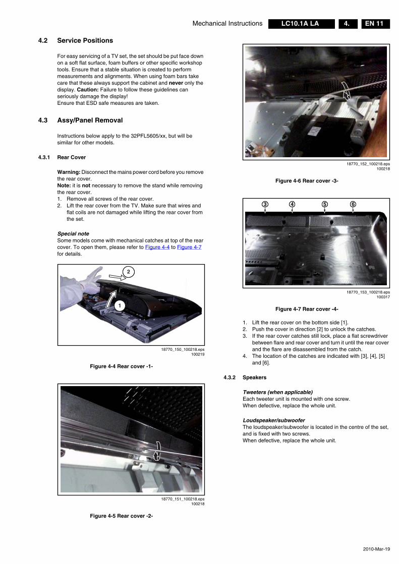
4.3.3 Main Power Supply
Refer to Figure 4-8 for details.
Figure 4-8 Main Power Supply
1. Unplug all connectors [1].2. Remove the fixation screws [2].3. Take the board out.When defective, replace the whole unit. Be aware to (re)place the spacers [3].
4.3.4 Small Signal Board (SSB)
Refer to Figure 4-9 for details.
Figure 4-9 SSB
1. Unplug all connectors [1] and [2].2. Remove the fixation screws [3].3. Take the board out.When defective, replace the whole unit.
4.3.5 Mains Switch
The mains switch assy is mounted below the PSU on the front bezel with two screws. When replacing the switch, remove it from its bracket.
4.3.6 IR & LED Board
Refer to Figure 4-10, Figure 4-11 and Figure 4-12 for details.
Figure 4-10 IR & LED Board -1-
Figure 4-11 IR & LED Board -2-
Figure 4-12 IR & LED Board -3-
1. Remove the stand [1].2. Remove the IR & LED board cover [2].3. Release the clips [3] that secure the IR & LED board.4. Remove the connectors [4] on the IR/LED board.
18920_103_100317.eps100317
1
1
2
2
2
2
2
2
1
3
3
18920_104_100317.eps100317
2
2
1
3
33
3
3
18770_142_100215.eps100215
1
1
1
1
18770_143_100215.eps100215
2
18770_144_100215.eps100215
4
33
Mechanical Instructions EN 13LC10.1A LA 4.
2010-Mar-19
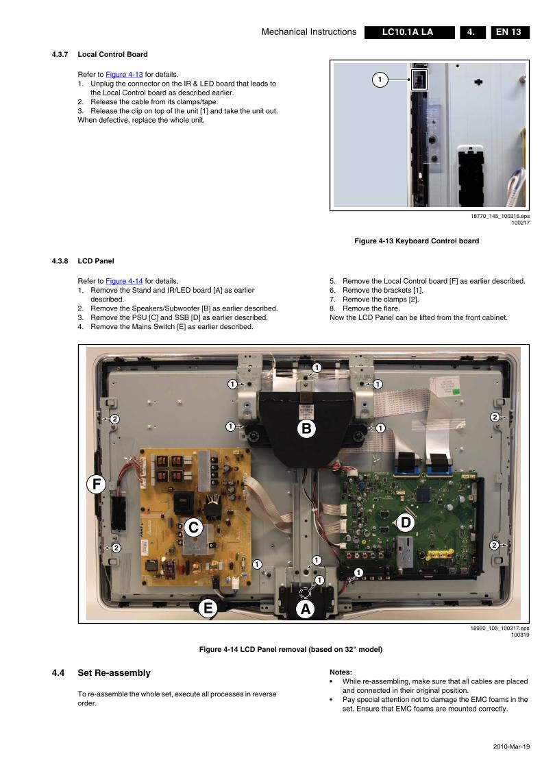
4.3.7 Local Control Board
Refer to Figure 4-13 for details.1. Unplug the connector on the IR & LED board that leads to
the Local Control board as described earlier.2. Release the cable from its clamps/tape.3. Release the clip on top of the unit [1] and take the unit out.When defective, replace the whole unit.
Figure 4-13 Keyboard Control board
4.3.8 LCD Panel
Refer to Figure 4-14 for details.1. Remove the Stand and IR/LED board [A] as earlier
described.2. Remove the Speakers/Subwoofer [B] as earlier described.3. Remove the PSU [C] and SSB [D] as earlier described.4. Remove the Mains Switch [E] as earlier described.
5. Remove the Local Control board [F] as earlier described.6. Remove the brackets [1].7. Remove the clamps [2].8. Remove the flare.Now the LCD Panel can be lifted from the front cabinet.
Figure 4-14 LCD Panel removal (based on 32" model)
4.4 Set Re-assembly
To re-assemble the whole set, execute all processes in reverse order.
Notes:• While re-assembling, make sure that all cables are placed
and connected in their original position. • Pay special attention not to damage the EMC foams in the
set. Ensure that EMC foams are mounted correctly.
18770_145_100216.eps100217
1
18920_105_100317.eps100319
1
11
1
2
2
1
2
2
1
1
1
C D
A
B
E
1
F

Service Modes, Error Codes, and Fault FindingEN 14 LC10.1A LA5.
2010-Mar-19
5. Service Modes, Error Codes, and Fault Finding
Index of this chapter:5.1 Test Points5.2 Service Modes5.3 Service Tools5.4 Error Codes5.5 The Blinking LED Procedure5.6 Fault Finding and Repair Tips5.7 Software Upgrading
5.1 Test Points
In the chassis schematics and layout overviews, the test points are mentioned. In the schematics, test points are indicated with “Fxxx” or “Ixxx”, in the layout overviews with a “half-moon” sign.As most signals are digital, it will be difficult to measure waveforms with a standard oscilloscope. Several key ICs are capable of generating test patterns, which can be controlled via ComPair. In this way it is possible to determine which part is defective. Perform measurements under the following conditions:• Service Default Mode.• Video: Colour bar signal.• Audio: 3 kHz left, 1 kHz right.
5.2 Service Modes
The Service Mode feature is split into four parts: • Service Default Mode (SDM).• Service Alignment Mode (SAM).• Customer Service Mode (CSM).• Computer Aided Repair Mode (ComPair). SDM and SAM offer features, which can be used by the Service engineer to repair/align a TV set. Some features are: • A pre-defined situation to ensure measurements can be
made under uniform conditions (SDM).• Activates the blinking LED procedure for error identification
when no picture is available (SDM).• The possibility to overrule software protections when SDM
is entered via the Service pins.• Make alignments (e.g. White Tone), (de)select options,
enter options codes, reset the error buffer (SAM).• Display information (“SDM” or “SAM” indication in upper
right corner of screen, error buffer, software version, operating hours, options and option codes, sub menus).
The CSM is a Service Mode that can be enabled by the consumer. The CSM displays diagnosis information, which the customer can forward to the dealer or call centre. In CSM mode, “CSM”, is displayed in the top right corner of the screen. The information provided in CSM and the purpose of CSM is to:• Increase the home repair hit rate.• Decrease the number of nuisance calls.• Solved customers' problem without home visit. ComPair Mode is used for communication between a computer and a TV on I2C /UART level and can be used by a Service engineer to quickly diagnose the TV set by reading out error codes, read and write in NVMs, communicate with ICs and the uP (PWM, registers, etc.), and by making use of a fault finding database. It will also be possible to up and download the software of the TV set via I2C with help of ComPair. To do this, ComPair has to be connected to the TV set via the ComPair connector, which will be accessible through the rear of the set (without removing the rear cover).
5.2.1 General
Some items are applicable to all Service Modes or are general. These are listed below.
Life TimerDuring the life time cycle of the TV set, a timer is kept (called “Op. Hour”). It counts the normal operation hours (not the Stand-by hours). The actual value of the timer is displayed in SDM and SAM in a decimal value. Every two soft-resets increase the hour by +1. Standby hours are not counted.
Software Identification, Version, and ClusterThe software ID, version, and cluster will be shown in the main menu display of SDM, SAM, and CSM.The screen will show: “AAAAAB XX.YY”, where: • AAAAA is the chassis name: LC101.• B is the region indication: E= Europe, A= AP/China, U=
NAFTA, L= LATAM.• XX is the main version number: this is updated with a major
change of specification (incompatible with the previous software version). Numbering will go from 01 - 99 and AA - ZZ.– If the main version number changes, the new version
number is written in the NVM.– If the main version number changes, the default
settings are loaded.• YY is the sub version number: this is updated with a minor
change (backwards compatible with the previous versions) Numbering will go from 00 - 99.– If the sub version number changes, the new version
number is written in the NVM.– If the NVM is fresh, the software identification, version,
and cluster will be written to NVM.
Display Option Code SelectionWhen after an SSB or display exchange, the display option code is not set properly, it will result in a TV with “no display”. Therefore, it is required to set this display option code after such a repair.To do so, press the following key sequence on a standard RC transmitter: “062598” directly followed by MENU/HOME and “xxx”, where “xxx” is a 3 digit decimal value of the panel type: see column “Display Code” in Table 6-5 , or see sticker on the side/bottom of the cabinet. When the value is accepted and stored in NVM, the set will switch to Stand-by, to indicate that the process has been completed.
Figure 5-1 Location of Display Option Code sticker
During this algorithm, the NVM-content must be filtered, because several items in the NVM are TV-related and not SSB-related (e.g. Model and Prod. S/N). Therefore, “Model” and “Prod. S/N” data is changed into “See Type Plate”.
10000_038_090121.eps090819
PHILIPSMODEL:32PF9968/10
PROD.SERIAL NO:
AG 1A0620 000001
040
39mm
27m
m
(CTN Sticker)
Display OptionCode

Service Modes, Error Codes, and Fault Finding EN 15LC10.1A LA 5.
2010-Mar-19
In case a call centre or consumer reads “See Type Plate” in CSM mode, he needs to look to the side/bottom sticker to identify the set, for further actions.
5.2.2 Service Default Mode (SDM)
PurposeSet the TV in SDM mode in order to be able to create a pre-defined setting for measurements to be made. In this platform, a simplified SDM is introduced (without protection override and without tuning to a frequency of 475.25 MHz).
Specifications• Set linear video and audio settings to 50%, but volume to
25%. Stored user settings are not affected.• All service-unfriendly modes (if present) are disabled, since
they interfere with diagnosing/repairing a set. These service unfriendly modes are:– (Sleep) timer.– Blue mute/Wall paper.– Auto switch “off” (when there is no “ident” signal).– Hotel or hospital mode.– Child lock or parental lock (manual or via V-chip).– Skipping, blanking of “Not favourite”, “Skipped” or
“Locked” presets/channels.– Automatic storing of Personal Preset or Last Status
settings.– Automatic user menu time-out (menu switches back/
OFF automatically.– Auto Volume levelling (AVL).
How to ActivateTo activate SDM, use one of the following methods:• Press the following key sequence on the remote control
transmitter: “062596” directly followed by the MENU button (do not allow the display to time out between entries while keying the sequence).
• Short one of the “Service” pads on the TV board during cold start (see Figure 5-2). Then press the mains button (remove the short after start-up). Caution: When doing this, the service-technician must know exactly what he is doing, as it could damage the television set.
Figure 5-2 Service pads (SSB component side)
On Screen MenuAfter activating SDM, the following items are displayed, with “SDM” in the upper right corner of the screen to indicate that the television is in Service Default Mode.Menu items and explanation:• xx.x hrs: Operating hours (in decimal).• AAAAAB XX.YY: See paragraph Software Identification,
Version, and Cluster for the SW name definition.
• ERR: Shows all errors detected since the last time the buffer was erased in format <xxx> <xxx> <xxx> <xxx> <xxx> (five errors possible).
• OP: Used to read-out the option bytes. See “Options” in the Alignments section for a detailed description. Ten codes (in two rows) are possible.
How to NavigateAs this mode is read only, there is not much to navigate. To switch to other modes, use one of the following methods:• Command MENU from the user remote will enter the
normal user menu (brightness, contrast, colour, etc...) with “SDM” OSD remaining, and pressing MENU key again will return to the last status of SDM again.
• To prevent the OSD from interfering with measurements in SDM, command “OSD” or “i+” (“STATUS” or “INFO” for NAFTA and LATAM) from the user remote will toggle the OSD “on/off” with “SDM” OSD remaining always “on”.
• Press the following key sequence on the remote control transmitter: “062596” directly followed by the OSD/STATUS/INFO/i+ button to switch to SAM (do not allow the display to time out between entries while keying the sequence).
How to ExitSwitch the set to STANDBY by pressing the mains button on the remote control transmitter or on the television set.If you switch the television set “off” by removing the mains (i.e., unplugging the television), the television set will remain in SDM when mains is re-applied, and the error buffer is not cleared.The error buffer will only be cleared when the “clear” command is used in the SAM menu.
Note:• If the TV is switched “off” by a power interrupt while in SDM,
the TV will show up in the last status of SDM menu as soon as the power is supplied again. The error buffer will not be cleared.
• In case the set is accidentally in Factory mode (with an “F” displayed on the screen), pressing and holding “VOL-“ and “CH-” simultaneously should exit the Factory mode.
5.2.3 Service Alignment Mode (SAM)
Purpose• To change option settings.• To display / clear the error code buffer. • To perform alignments.
Specifications• Operation hours counter (maximum five digits displayed).• Software version, error codes, and option settings display.• Error buffer clearing.• Option settings.• Software alignments (White Tone).• NVM Editor.• Set screen mode to full screen (all content is visible).
How to ActivateTo activate SAM, use one of the following methods:• Press the following key sequence on the remote control
transmitter: “062596” directly followed by the OSD/STATUS/INFO/i+ button (it depends on region which button is present on the RC). Do not allow the display to time out between entries while keying the sequence.
• Or via ComPair. After entering SAM, the following items are displayed, with “SAM” in the upper right corner of the screen to indicate that the television is in Service Alignment Mode.
18920_201_100317.eps100317
SDMSDM

Service Modes, Error Codes, and Fault FindingEN 16 LC10.1A LA5.
2010-Mar-19
Menu items and explanation:1. System Inform.
• Op Hour: This represents the life timer. The timer counts normal operation hours, but does not count Stand-by hours.
• MAIN SW ID: See paragraph Software Identification, Version, and Cluster for the SW name definition.
• ERR: Shows all errors detected since the last time the buffer was erased. Five errors possible.
• OP1 / OP2: Used to read-out the option bytes. See paragraph 6.5 Option Settings in the Alignments section for a detailed description. Ten codes are possible.
2. Clear Codes. Erases the contents of the error buffer. Select this menu item and press the MENU RIGHT key on the remote control. The content of the error buffer is cleared.
3. Options. To set the option bits. See paragraph 6.5 Option Settings in the “Alignments” chapter for a detailed description.
4. RGB Alignment. To align the White Tone. See White Tone Alignment: for a detailed description.
5. NVM Editor. To change the NVM data in the television set. See also paragraph 5.6 Fault Finding and Repair Tips.
6. NVM Copy. Gives the possibility to copy/load the NVM file to/from an USB stick. NVM data copied to a USB memory device is named “NVM_COPY.BIN”. When copied back to a TV, the file first must have the same name.
7. Tuner. • AGC Adjustment: See paragraph 6.3.1 for
instructions.• Store: To store the data.
8. Auto ADC. Refer to chapter 6. Alignments for detailed information.
9. EDID Write Enable. Enables EDID writing.
How to Navigate• In the SAM menu, select menu items with the UP/DOWN
keys on the remote control transmitter. The selected item will be indicated. When not all menu items fit on the screen, use the UP/DOWN keys to display the next / previous menu items.
• With the LEFT/RIGHT keys, it is possible to:– Activate the selected menu item.– Change the value of the selected menu item.– Activate the selected sub menu.
• When you press the MENU button twice while in top level SAM, the set will switch to the normal user menu (with the SAM mode still active in the background). To return to the SAM menu press the MENU button.
• The “OSD/STATUS/INFO/i+” key from the user remote will toggle the OSD “on/off” with “SAM” OSD remaining always “on”.
• Press the following key sequence on the remote control transmitter: “062596” directly followed by the MENU button to switch to SDM (do not allow the display to time out between entries while keying the sequence).
How to Store SAM SettingsTo store the settings changed in SAM mode (except the OPTIONS and RGB ALIGN settings), leave the top level SAM menu by using the POWER button on the remote control transmitter or the television set. The mentioned exceptions must be stored separately via the STORE button.
How to ExitSwitch the set to STANDBY by pressing the mains button on the remote control transmitter or the television set.
Note:• When the TV is switched “off” by a power interrupt while in
SAM, the TV will show up in “normal operation mode” as soon as the power is supplied again. The error buffer will not be cleared.
• In case the set is in Factory mode by accident (with “F” displayed on screen), by pressing and hold “VOL-“ and “CH-” together should leave Factory mode.
5.2.4 Customer Service Mode (CSM)
PurposeThe Customer Service Mode shows error codes and information on the TV’s operation settings. A call centre can instruct the customer (by telephone) to enter CSM in order to identify the status of the set. This helps them to diagnose problems and failures in the TV before making a service call.The CSM is a read-only mode; therefore, modifications are not possible in this mode.
Specifications• Ignore “Service unfriendly modes”.• Line number for every line (to make CSM language
independent).• Set the screen mode to full screen (all contents on screen
is visible).• After leaving the Customer Service Mode, the original
settings are restored.• Possibility to use “CH+” or “CH-” for channel surfing, or
enter the specific channel number on the RC.
How to ActivateTo activate CSM, press the following key sequence on a standard remote control transmitter: “123654” (do not allow the display to time out between entries while keying the sequence). After entering the Customer Service Mode, the following items are displayed:
Menu Explanation CSM11. Set Type. Type number, e.g. 32PFL5605/93. (*)2. Production code. Product serial no., e.g.
BZ1A1008123456 (*). BZ= Production centre, 1= BOM code, A= Service version change code, 10= Production year, 08= Production week, 123456= Serial number.
3. not used4. - Option Code 1. Option code information (group 1).
- Option Code 2. Option code information (group 2).5. SSB. Indication of the SSB factory ID (= 12nc). (*)6. Display. Indication of the display ID (=12 nc). (*)7. PSU. Indication of the PSU factory ID (= 12nc).
(*) If an NVM IC is replaced or initialized, these items must be re-written to the NVM. ComPair will foresee in a possibility to do this.
Menu Explanation CSM21. Current Main SW. Shows the main software version.2. Standby SW. Shows the standby software version.3. MT8282 SW. Shows the MT8282 software version.4. Bootloader ID. Shows the Bootloader software ID.5. NVM Version. The NVM software version no.6. Flash ID. Shows the flash ID.
Menu Explanation CSM31. Signal Quality. Shows the signal quality (No Signal/
POOR/AVERAGE/GOOD).2. not used3. Key (HDCP). Indicates if the HDMI keys (or HDCP keys)
are valid or not.4. not used5. not used6. HDMI audio format input stream. Specification of HDMI
audio input stream.7. HDMI video format input stream. Specification of HDMI
video input stream.

Service Modes, Error Codes, and Fault Finding EN 17LC10.1A LA 5.
2010-Mar-19
How to ExitTo exit CSM, use one of the following methods:• Press the MENU/HOME button on the remote control
transmitter.• Press the POWER button on the remote control
transmitter.• Press the POWER button on the television set.
5.3 Service Tools
5.3.1 ComPair
IntroductionComPair (Computer Aided Repair) is a Service tool for Philips Consumer Electronics products. and offers the following:1. ComPair helps you to quickly get an understanding on how
to repair the chassis in a short and effective way.2. ComPair allows very detailed diagnostics and is therefore
capable of accurately indicating problem areas. You do not have to know anything about I2C or UART commands yourself, because ComPair takes care of this.
3. ComPair speeds up the repair time since it can automatically communicate with the chassis (when the uP is working) and all repair information is directly available.
4. ComPair features TV software up possibilities.
SpecificationsComPair consists of a Windows based fault finding program and an interface box between PC and the (defective) product. The (new) ComPair II interface box is connected to the PC via an USB cable. For the TV chassis, the ComPair interface box and the TV communicate via a bi-directional cable via the service connector(s).
How to ConnectThis is described in the ComPair chassis fault finding database.
Figure 5-3 ComPair II interface connection
Caution: It is compulsory to connect the TV to the PC as shown in the picture above (with the ComPair interface in between), as the ComPair interface acts as a level shifter. If one connects the TV directly to the PC (via UART), ICs will be blown!
How to OrderComPair II order codes:• ComPair II interface: 3122 785 91020.• ComPair UART interface cable: 3138 188 75051.
• Program software can be downloaded from the Philips Service website.
Additional cables for VCOM Alignment• ComPair/I2C interface cable: 3122 785 90004.• ComPair/VGA adapter cable: 9965 100 09269.
Note: If you encounter any problems, contact your local support desk.
5.4 Error Codes
5.4.1 Introduction
Error codes are required to indicate failures in the TV set. In principle a unique error code is available for every:• Activated (SW) protection.• Failing I2C device.• General I2C error. The last five errors, stored in the NVM, are shown in the Service menu’s. This is called the error buffer.The error code buffer contains all errors detected since the last time the buffer was erased. The buffer is written from left to right. When an error occurs that is not yet in the error code buffer, it is displayed at the left side and all other errors shift one position to the right.An error will be added to the buffer if this error differs from any error in the buffer. The last found error is displayed on the left.An error with a designated error code may never lead to a deadlock situation. This means that it must always be diagnosable (e.g. error buffer via OSD or blinking LED procedure, ComPair to read from the NVM).In case a failure identified by an error code automatically results in other error codes (cause and effect), only the error code of the MAIN failure is displayed. Example: In case of a failure of the I2C bus (CAUSE), the error code for a “General I2C failure” and “Protection errors” is displayed. The error codes for the single devices (EFFECT) is not displayed. All error codes are stored in the same error buffer (TV’s NVM) except when the NVM itself is defective.
5.4.2 How to Read the Error Buffer
You can read the error buffer in 3 ways:• On screen via the SAM/SDM/CSM (if you have a picture).
Example:– ERROR: 0 0 0 0 0 : No errors detected– ERROR: 6 0 0 0 0 : Error code 6 is the last and only
detected error– ERROR: 9 6 0 0 0 : Error code 6 was detected first and
error code 9 is the last detected (newest) error• Via the blinking LED procedure (when you have no
picture). See paragraph 5.5 The Blinking LED Procedure.• Via ComPair.
5.4.3 Error codes
The “layer 1” error codes are pointing to the defective board. They are triggered by LED blinking when CSM is activated. In the LC10 platform, only two boards are present: the SSB and the PSU, meaning only three layer 1 errors are defined:• 2: SSB• 3: PSU• 4: POK line defective.
The following “layer 2” errors have been assigned:• 00: no error• 11: DC protection of speakers; leads to “Protection”• 16: +12V protection error (or 12V failure), PSU defective;
leads to “Protection”• 18: POK line error; leads to “Error”
10000_036_090121.eps091118
TOUART SERVICECONNECTOR
TOUART SERVICECONNECTOR
TOI2C SERVICECONNECTOR
TO TV
PC
HDMII2C only
Optional power5V DC
ComPair II Developed by Philips Brugge
RC outRC in
OptionalSwitch
Power ModeLink/Activity I2C
ComPair IIMulti
function
RS232 /UART
Service Modes, Error Codes, and Fault FindingEN 18 LC10.1A LA5.
2010-Mar-19
• 21: Post video processing IC (MT8282); leads to “Error”• 27: I2C bus error IF demodulator; leads to “Error”• 34: Tuner I2C bus error; leads to “Error”• 35: EEPROM I2C bus error (M24C16); leads to “Protection”
5.4.4 How to Clear the Error Buffer
The error code buffer is cleared in the following cases:• By using the CLEAR command in the SAM menu:• If the contents of the error buffer have not changed for 50
hours, the error buffer resets automatically. Note: If you exit SAM by disconnecting the mains from the television set, the error buffer is not reset.
5.5 The Blinking LED Procedure
5.5.1 Introduction
The software is capable of identifying different kinds of errors. Because it is possible that more than one error can occur over time, an error buffer is available, which is capable of storing the last five errors that occurred. This is useful if the OSD is not working properly. Errors can also be displayed by the blinking LED procedure. The method is to repeatedly let the front LED pulse with as many pulses as the error code number, followed by a period of 1.5 seconds in which the LED is “off”. Then this sequence is repeated. Example (1): error code 4 will result in four times the sequence LED “on” for 0.25 seconds / LED “off” for 0.25 seconds. After this sequence, the LED will be “off” for 1.5 seconds. Any RC5 command terminates the sequence. Error code LED blinking is in red colour. Example (2): the content of the error buffer is “12 9 6 0 0” After entering SDM, the following occurs: • 1 long blink of 5 seconds to start the sequence,• 12 short blinks followed by a pause of 1.5 seconds,• 9 short blinks followed by a pause of 1.5 seconds,• 6 short blinks followed by a pause of 1.5 seconds,• 1 long blink of 1.5 seconds to finish the sequence,• The sequence starts again with 12 short blinks.
5.5.2 Displaying the Entire Error Buffer
Additionally, the entire error buffer is displayed when Service Mode “SDM” is entered. In case the TV set is in protection or Stand-by: The blinking LED procedure sequence (as in SDM-mode in normal operation) must be triggered by the following RC sequence: “MUTE” “062500” “OK”.In order to avoid confusion with RC5 signal reception blinking, this blinking procedure is terminated when a RC5 command is received.
5.6 Fault Finding and Repair Tips
Notes: • It is assumed that the components are mounted correctly
with correct values and no bad solder joints. • Before any fault finding actions, check if the correct
options are set.
5.6.1 NVM Editor
In some cases, it can be convenient if one directly can change the NVM contents. This can be done with the “NVM Editor” in SAM mode. With this option, single bytes can be changed.
Caution: • Do not change these, without understanding the
function of each setting, because incorrect NVM settings may seriously hamper the correct functioning of the TV set!
• Always write down the existing NVM settings, before changing the settings. This will enable you to return to the original settings, if the new settings turn out to be incorrect.
5.6.2 Load Default NVM Values
It is possible to download default values automatically into the NVM in case a blank NVM is placed or when the NVM first 20 address contents are “FF”. After the default values are downloaded, it is possible to start-up and to start aligning the TV set. To initiate a forced default download the following action has to be performed:1. Switch “off” the TV set with the mains cord disconnected
from the wall outlet (it does not matter if this is from “Stand-by” or “Off” situation).
2. Short-circuit the SDM pads on the SSB (keep short circuited, see Figure 5-2).
3. Press “P+” or “CH+” on the local keyboard (and keep it pressed).
4. Reconnect the mains supply to the wall outlet.5. Release the “P+” or “CH+” when the set is started up and
has entered SDM.When the downloading has completed successfully, the set will perform a restart. After this, put the set to standby and remove the short-circuit on the SDM pads.
Alternative method:It is also possible to upload the default values to the NVM with ComPair in case the SW is changed, the NVM is replaced with a new (empty) one, or when the NVM content is corrupted.After replacing an EEPROM (or with a defective/no EEPROM), default settings should be used to enable the set to start-up and allow the Service Default Mode and Service Alignment Mode to be accessed.
5.6.3 Fault finding tips Tuner Section
When there is no picture in analog RF mode:• Check if supply voltages 5 V are present at test points
F205, F206 and F231.• Check whether picture is present in AV.• Check if I2C lines are working properly (3.3 V).• Store a known channel manually and check if there is an IF
output signal at the tuner pin 12. If not, the tuner may be faulty.
• Feed-in a 105 dBuV signal at the tuner pin 12 and check whether there is an CVBS output signal from the IF demodulator. If not, the IF demodulator may be faulty. Check the components in this area.
Service Modes, Error Codes, and Fault Finding EN 19LC10.1A LA 5.
2010-Mar-19
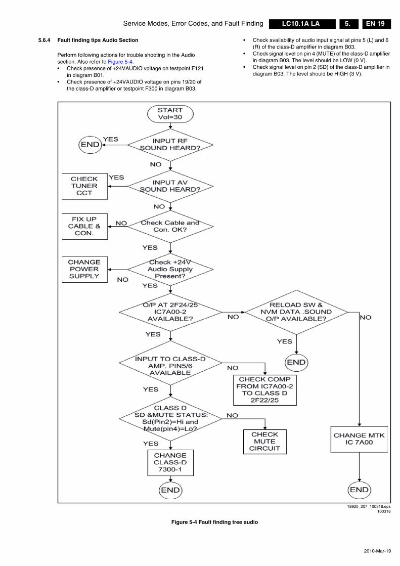
5.6.4 Fault finding tips Audio Section
Perform following actions for trouble shooting in the Audio section. Also refer to Figure 5-4.• Check presence of +24VAUDIO voltage on testpoint F121
in diagram B01.• Check presence of +24VAUDIO voltage on pins 19/20 of
the class-D amplifier or testpoint F300 in diagram B03.
• Check availability of audio input signal at pins 5 (L) and 6 (R) of the class-D amplifier in diagram B03.
• Check signal level on pin 4 (MUTE) of the class-D amplifier in diagram B03. The level should be LOW (0 V).
• Check signal level on pin 2 (SD) of the class-D amplifier in diagram B03. The level should be HIGH (3 V).
Figure 5-4 Fault finding tree audio
18920_207_100318.eps100318

Service Modes, Error Codes, and Fault FindingEN 20 LC10.1A LA5.
2010-Mar-19
5.7 Software Upgrading
5.7.1 Introduction
It is possible for the user to upgrade the main software via the USB port. This allows replacement of a software image in a stand alone set. A description on how to upgrade the main software can be found in the DFU or on the Philips website.
5.7.2 Main Software Upgrade
Automatic Software UpgradeIn “normal” conditions, so when there is no major problem with the TV, the main software and the default software upgrade application can be upgraded with the “autorun.upg” (FUS part in the one-zip file). This can also be done by the consumers themselves, but they will have to get their software from the commercial Philips website or via the Software Update Assistant in the user menu (see DFU). The “autorun.upg” file must be placed in the root of your USB stick. How to upgrade:1. Copy “autorun.upg” to the root of your USB stick.2. Insert USB stick in the side I/O while the set is in “On”
mode. The “Menu” icon will be prompted automatically. Go to the “Setup” menu for local updates. The TV will prompt the “upgrade” message; press “Acknowledge” to continue, after which the upgrading will start automatically. As soon as the programming is finished, the set will restart. In the “Setup” menu you can check if the latest software is running.
5.7.3 Content and Usage of the One-Zip Software File
Below you find a content explanation of the One-Zip file, and instructions on how and when to use it. Only files that are relevant for Service are mentioned here!
• EDID_clustername_version.zip. Contains the EDID content of the different EDID NVMs. See ComPair for further instructions.
• FUS_clustername_version.zip. Contains the “autorun.upg” which is needed to upgrade the TV main software and the software download application.
• NVM_clustername_version.zip. Default NVM content. Must be programmed via ComPair.
5.7.4 How to Copy NVM Data to/from USB
Write NVM data to USB1. Insert the USB stick into the USB slot while in SAM mode.2. Execute the command "NVM Copy" > "NVM Copy to USB",
to copy the NVM data to the USB stick. The NVM filename on the USB stick will be named "NMLC101A.BIN" (this takes a couple of seconds).
Write NVM data to TV1. First, ensure (via a PC) that the filename on the USB stick
has the correct format: "NMLC101A.BIN".2. Insert the USB stick into the USB slot while in SAM mode.3. Execute the command "NVM Copy" > "NVM Copy from
USB" to copy the USB data to NVM (this takes about a minute to complete).
Important: The file must be located in the root directory of the USB stick.
Alignments EN 21LC10.1A LA 6.
2010-Mar-19
6. Alignments
Index of this chapter:6.1 General Alignment Conditions6.2 Hardware Alignments6.3 Software Alignments6.4 ADC gain adjustment6.5 Option Settings Note: Figures below can deviate slightly from the actual situation, due to the different set executions.
General: The Service Default Mode (SDM) and Service Alignment Mode (SAM) are described in chapter 5. Menu navigation is done with the CURSOR UP, DOWN, LEFT or RIGHT keys of the remote control transmitter.
6.1 General Alignment Conditions
Perform all electrical adjustments under the following conditions:• Power supply voltage (depends on region):
– AP-NTSC: 120 VAC or 230 VAC / 50 Hz (± 10%).– AP-PAL-multi: 120 - 230 VAC / 50 Hz (± 10%).– EU: 230 VAC / 50 Hz (± 10%). – LATAM-NTSC: 120 - 230 VAC / 50 Hz (± 10%).– US: 120 VAC / 60 Hz (± 10%).
• Connect the set to the mains via an isolation transformer with low internal resistance.
• Allow the set to warm up for approximately 15 minutes.• Measure voltages and waveforms in relation to correct
ground (e.g. measure audio signals in relation to AUDIO_GND). Caution: It is not allowed to use heatsinks as ground.
• Test probe: Ri > 10 Mohm, Ci < 20 pF.• Use an isolated trimmer/screwdriver to perform
alignments.
6.2 Hardware Alignments
There are no hardware alignments foreseen for this chassis, but below find an overview of the most important DC voltages on the SSB. These can be used for checking proper functioning of the DC/DC converters.
6.3 Software Alignments
With the software alignments of the Service Alignment Mode (SAM) the Tuner and RGB settings can be aligned.
6.3.1 Tuner Adjustment (RF AGC Take Over Point)
Purpose: To keep the tuner output signal constant as the input signal amplitude varies.
The LC10.1A LA chassis comes with the VA1E8CD501 analogue tuner. No alignment is necessary, as the AGC alignment is done automatically (standard value: “18”). However in case of problems use the following method (use multimeter and RF generator):• Apply a vision IF carrier of 38.9 MHz (105 dBuV = 178
mVrms) to injection point A210 (input via 50 ohm coaxial cable terminated with an RC network of series 10nF with 120 ohm to ground).
• Measure voltage on pin 3 of the tuner (test point F229).• Adjust AGC (via SAM menu: TUNER -> AGC), until voltage
on pin 3 is 3.3 +0.5/-1.0 V.• Store settings and exit SAM.
6.3.2 RGB Alignment
Before alignment, choose “Setup” -> “Picture” and set:• “Brightness” to “50”.• “Colour” to “50”.• “Contrast” to “100”.
White Tone Alignment:• Activate SAM.• Select “RGB Alignment“ and choose a colour temperature.• Use a 100% white screen as input signal and set the
following values: – All “White point” values initial to “256”.
In case you have a colour analyser:• Measure with a calibrated (phosphor- independent) colour
analyser (e.g. Minolta CA-210) in the centre of the screen. Consequently, the measurement needs to be done in a dark environment.
• Adjust the correct x,y coordinates (while holding one of the White point registers R, G or B on “256”) by means of decreasing the value of one or two other white points to the correct x,y coordinates (see Table 6-1 White D alignment values). Tolerance: dx: ± 0.004, dy: ± 0.004.
• Repeat this step for the other colour Temperatures that need to be aligned.
• When finished return to the SAM root menu and press STANDBY on the RC to store the aligned values to the NVM.
Table 6-1 White D alignment values
If you do not have a colour analyser, you can use the default values. This is the next best solution. The default values are average values coming from production (statistics).• Set the RED, GREEN and BLUE default values per
temperature according to the values in the “Tint settings” table.
Description Test Point Specifications (V) Diagram
Min. Typ. Max.
+12VS F118/F119/F120
11.40 12.00 12.60 B01_DC-DC
+3V3_STBY F113 3.20 3.30 3.40 B01_DC-DC
+3V3_SW F131 3.14 3.3 3.46 B01_DC-DC
+1V1_SW F126 1.18 1.25 1.31 B01_DC-DC
+5V_SW F130 4.94 5.2 5.46 B01_DC-DC
+1V8_SW F125 1.71 1.80 1.89 B01_DC-DC
+5V_HDMI F130 4.94 5.2 5.46 B01_DC-DC
+12VDISP F102 11.40 12.00 12.60 B01_DC-DC
+5VTUN F205 4.94 5.2 5.46 B02_Tuner + DeMod
+5VS F206 4.94 5.2 5.46 B02_Tuner + DeMod
+24VAUDIO F121 21.6 24 26.4 B01_DC-DC
VLS_15V6 FKFD tbd 15.6 tbd B08B_TCON_DC-DC
VGH_35V FKFA 34.0 35.0 36.0 B08B_TCON_DC-DC
VGL_-6V FKFK -7.0 -6.0 -5.0 B08B_TCON_DC-DC
VCC_3V3 FKFB tbd 3.3 tbd B08B_TCON_DC-DC
VCC_1V2 FKDD 1.1 1.2 1.3 B08A_TCON_CONTROL
Value Cool (11000 K) Normal (9000 K) Warm (6500 K)
x 0.276 0.287 0.313
y 0.282 0.296 0.329

AlignmentsEN 22 LC10.1A LA6.
2010-Mar-19
• When finished return to the SAM root menu and press STANDBY on the RC to store the aligned values to the NVM.
Table 6-2 Tint settings 32"
Table 6-3 Tint settings 40"
Table 6-4 Tint settings 46"
6.4 ADC gain adjustment
Use a Quantum Data Patters Generator 802BT and apply a “PgcWrgb” image (“dot, cross and colour bar mix pattern”) according to Figure 6-1.
Figure 6-1 “PgcWrgb” pattern
6.4.1 YPbPr
Following instructions result in correct alignment of ADC gain, offset and phase, related to YPbPr input signal. Apply a signal of format “1080i25”.• Apply following signals to the YPbPr input connectors:
– Pr signal of 0.7 Vp-p1 / 75 ohm to the red cinch connector
– Y signal of 0.7 Vb-p2 / 75 ohm with a sync pulse of 0.3 Vp-p1 to the green cinch connector
– Pb signal of 0.7 Vb-p2 / 75 ohm to the blue cinch connector
• Select the input source to YPbPr input• In SAM, initiate the ADC calibration command.Upon appearance of the “Auto ADC Completed” message, the alignment is completed.
Notes:1. peak-to-peak2. black-to-peak.
6.4.2 PC VGA
Following instructions result in correct alignment of ADC gain, offset and phase, related to PC VGA input signal. Apply a signal of format “DMT1060”.• Apply following signals to the PC VGA input connector:
– Red signal of 650 - 730 mV– Green signal of 650 - 730 mV– Blue signal of 650 - 730 mV
• Select the input source to PC VGA input• In SAM, initiate the ADC calibration command.Upon appearance of the “Auto ADC Completed” message, the alignment is completed.
6.5 Option Settings
6.5.1 Introduction
The microprocessor communicates with a large number of I2C ICs in the set. To ensure good communication and to make digital diagnosis possible, the microprocessor has to know which ICs to address. The presence/absence of these specific ICs (or functions) is made known by the option codes. Notes: • After changing the option(s), save them with the STORE
command.• The new option setting becomes active after the TV is
switched “off” and “on” again with the mains switch (the EAROM is then read again).
6.5.2 How To Set Option Codes
When the NVM is replaced, all options will require resetting. To be certain that the factory settings are reproduced exactly, you must set all option numbers. You can find the correct option numbers in Table 6-5.
How to Change Options CodesAn option code (or “option byte”) represents eight different options (bits). When you change these numbers directly, you can set all options very quickly. All options are controlled via ten option bytes (OP1... OPA).Activate SAM and select “Options”. Now you can select the option byte (OP1 to OPA) with the CURSOR UP/ DOWN keys, and enter the new 3 digit (decimal) value. For the correct factory default settings, see Table 6-5 Option code overview. If an option is set (value “1”), it represents a certain decimal value.When all the correct options (bits) are set, the sum of the decimal values of each Option Byte (OP) will give the option code.
Table 6-5 Option code overview
Colour Temp. R G B
Cool tbf tbf tbf
Normal tbf tbf tbf
Warm tbf tbf tbf
Colour Temp. R G B
Cool tbf tbf tbf
Normal tbf tbf tbf
Warm tbf tbf tbf
Colour Temp. R G B
Cool tbf tbf tbf
Normal tbf tbf tbf
Warm tbf tbf tbf
18920_200_100317.eps100317
CTN Option Code Display Code
32PFL5605/93 016 029 239 191 056 000 000 000 000 002 233
32PFL5605/98 016 093 239 191 056 000 000 000 000 002 233
40PFL5605/93 016 029 239 191 056 000 000 000 000 001 234
40PFL5605/98 016 093 239 191 056 000 000 000 000 001 234
46PFL5605/67 016 093 239 191 056 000 000 000 000 001 236
46PFL5605/93 016 029 239 191 056 000 000 000 000 001 236
46PFL5605/98 016 093 239 191 056 000 000 000 000 001 236
Circuit Descriptions EN 23LC10.1A LA 7.
2010-Mar-19
7. Circuit Descriptions
Index of this chapter:7.1 Introduction7.2 LCD Power Supply7.3 Front-End7.4 Audio Processing7.5 TCON7.6 HDMI
Notes: • Only new circuits (circuits that are not published recently)
are described. • Figures can deviate slightly from the actual situation, due
to different set executions.• For a good understanding of the following circuit
descriptions, please use chapter 9. Block Diagrams and 10. Circuit Diagrams and PWB Layouts. Where necessary, you will find a separate drawing for clarification.
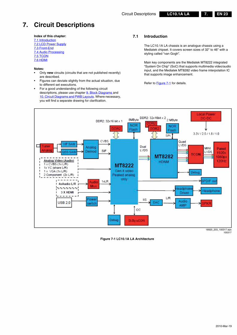
7.1 Introduction
The LC10.1A LA chassis is an analogue chassis using a Mediatek chipset. It covers screen sizes of 32" to 46" with a styling called “van Gogh”.
Main key components are the Mediatek MT8222 integrated “System On Chip” (SoC) that supports multimedia video/audio input, and the Mediatek MT8282 video frame interpolation IC that supports image enhancement.
Refer to Figure 7-1 for details.
Figure 7-1 LC10.1A LA Architecture
18920_203_100317.eps100317
Circuit DescriptionsEN 24 LC10.1A LA7.
2010-Mar-19
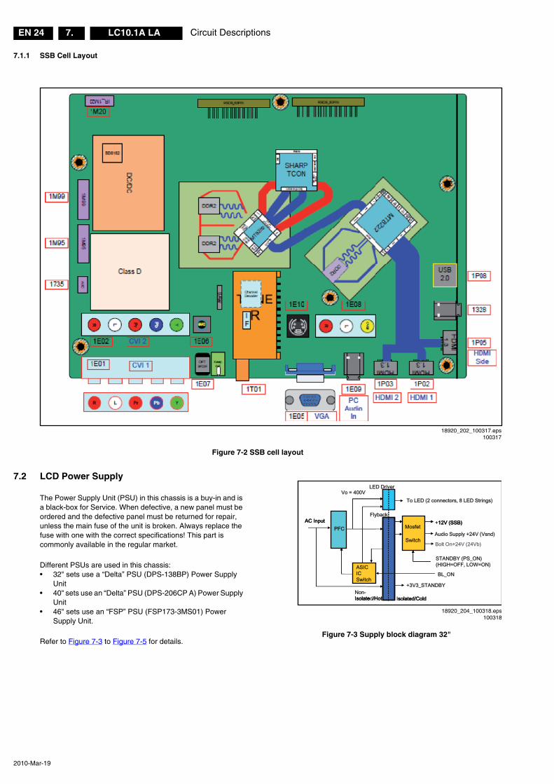
7.1.1 SSB Cell Layout
Figure 7-2 SSB cell layout
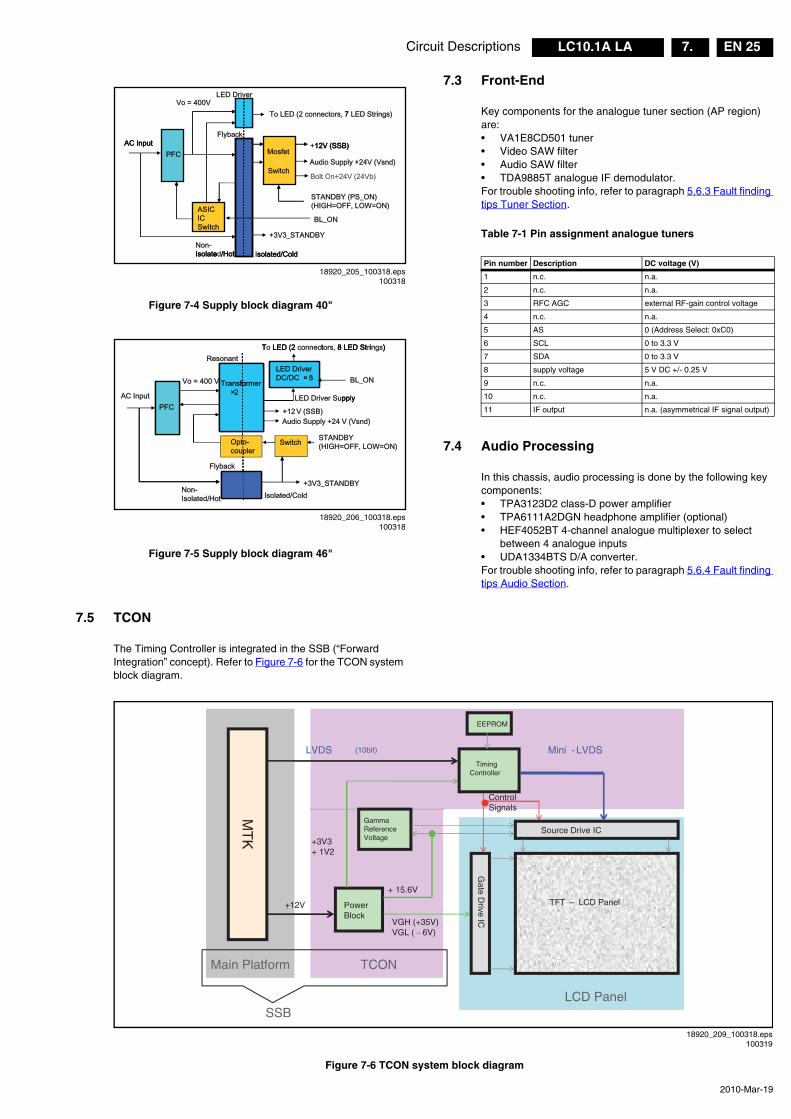
7.2 LCD Power Supply
The Power Supply Unit (PSU) in this chassis is a buy-in and is a black-box for Service. When defective, a new panel must be ordered and the defective panel must be returned for repair, unless the main fuse of the unit is broken. Always replace the fuse with one with the correct specifications! This part is commonly available in the regular market.
Different PSUs are used in this chassis:• 32" sets use a “Delta” PSU (DPS-138BP) Power Supply
Unit• 40" sets use an “Delta” PSU (DPS-206CP A) Power Supply
Unit• 46" sets use an “FSP” PSU (FSP173-3MS01) Power
Supply Unit.
Refer to Figure 7-3 to Figure 7-5 for details.Figure 7-3 Supply block diagram 32"
18920_202_100317.eps100317
18920_204_100318.eps100318
Circuit Descriptions EN 25LC10.1A LA 7.
2010-Mar-19
Figure 7-4 Supply block diagram 40"
Figure 7-5 Supply block diagram 46"
7.3 Front-End
Key components for the analogue tuner section (AP region) are:• VA1E8CD501 tuner• Video SAW filter• Audio SAW filter• TDA9885T analogue IF demodulator.For trouble shooting info, refer to paragraph 5.6.3 Fault finding tips Tuner Section.
Table 7-1 Pin assignment analogue tuners
7.4 Audio Processing
In this chassis, audio processing is done by the following key components:• TPA3123D2 class-D power amplifier• TPA6111A2DGN headphone amplifier (optional)• HEF4052BT 4-channel analogue multiplexer to select
between 4 analogue inputs• UDA1334BTS D/A converter.For trouble shooting info, refer to paragraph 5.6.4 Fault finding tips Audio Section.
7.5 TCON
The Timing Controller is integrated in the SSB (“Forward Integration” concept). Refer to Figure 7-6 for the TCON system block diagram.
Figure 7-6 TCON system block diagram
18920_205_100318.eps100318
18920_206_100318.eps100318
Pin number Description DC voltage (V)
1 n.c. n.a.
2 n.c. n.a.
3 RFC AGC external RF-gain control voltage
4 n.c. n.a.
5 AS 0 (Address Select: 0xC0)
6 SCL 0 to 3.3 V
7 SDA 0 to 3.3 V
8 supply voltage 5 V DC +/- 0.25 V
9 n.c. n.a.
10 n.c. n.a.
11 IF output n.a. (asymmetrical IF signal output)
18920_209_100318.eps100319
EEPROM
TFT – LCD Panel
Mini - LVDS
Control Signals
+3V3+ 1V2
VGH (+35V)VGL ( − 6V)
+12V
LVDS (10bit)
Timing Controller
Power Block
GammaReference Voltage
Source Drive IC
Gate D
rive IC
MT
K
LCD Panel
TCONMain Platform
SSB
+ 15.6V

Circuit DescriptionsEN 26 LC10.1A LA7.
2010-Mar-19
7.6 HDMI
7.6.1 Implementation
In this chassis, the main Mediatek MT8222 SoC has an on-chip HDMI multiplexer. Refer to Figure 7-7 for the HDMI implementation.
Figure 7-7 HDMI implementation
18920_208_100318.eps100318

IC Data Sheets EN 27LC10.1A LA 8.
2010-Mar-19
8. IC Data Sheets
This section shows the internal block diagrams and pin layouts of ICs that are drawn as "black boxes" in the electrical diagrams (with the exception of "memory" and "logic" ICs).
8.1 Diagram SSB: TUNER & Demodulator, Type TDA9886T (IC7212), Demodulator
Figure 8-1 Internal block diagram and pin configuration
G_16510_059.eps100318
Block diagram
Pinning information
TDA9885TDA9886
1
2
3
4
5
6
7
8
9
10
11
12
VIF1
VIF2
OP1
FMPLL
DEEM
AFD
DGND
AUD
TOP
SDA
SCL
SIOMAD
SIF2
SIF1
OP2
AFC
VP
VPLL
AGND
CVBS
VAGC(1)
REF
TAGC
n.c.
24
23
22
21
20
19
18
17
16
15
14
13
TAGC
CVAGC pos
CBL
VIF-PLL
4 MHz
external
AFC
video output 2 V (p-p)[1.1 V (p-p) without trap]
AUD
CAF
de-emphasisnetwork
FM-PLL filter
sound intercarrier output
CAGC
AGNDVP
VIF1
VIF-AGC RC VCO DIGITAL VCO CONTROL AFC DETECTOR
VIDEO TRAPS4.5 to 6.5 MHz
NARROW-BAND FM-PLLDETECTORI2C-BUS TRANSCEIVER
VIF-PLL
SINGLE REFERENCE QSS MIXER/INTERCARRIER MIXER AND
AM-DEMODULATOR
SIF-AGCSUPPLY
1
2
14 16 19 15 21
17
8
6
5
4127 11 101820
23
24
OUTPUTPORTS
MAD
AUDIO PROCESSINGAND SWITCHES
9
TUNER AGC
CAGC neg
3 22
crystal
and MAD select
TDA9885
n.c.
13
LLPMFDAMOISDNGDADSLCS2PO1PO
CVBS
TOP
VIF2
SIF1
SIF2 DEEM
AFD
REFVAGC VPLL
filter
TDA9886
(1)
(1) Not connected for TDA9885.
reference
or

IC Data SheetsEN 28 LC10.1A LA8.
2010-Mar-19
8.2 Diagram SSB: CLASS-D, Type TPA3123D2PWP (IC7300), Audio Amplifier
Figure 8-2 Internal block diagram and pin configuration
18440_302_090303.eps090318
Block diagram
Pinning information123456789101112
242322212019181716151413
PVCCLSD
PVCCLMUTE
LINRIN
BYPASSAGNDAGND
PVCCRVCLAMP
PVCCR
PGNDLPGNDLLOUTBSLAVCCAVCCGAIN0GAIN1BSRROUTPGNDRPGNDR
TERMINALI/O/P DESCRIPTION24-PINNAME (PWP)
Shutdown signal for IC (low = disabled, high = operational). TTL logic levels with compliance toSD 2 I AVCCRIN 6 I Audio input for right channelLIN 5 I Audio input for left channelGAIN0 18 I Gain select least-significant bit. TTL logic levels with compliance to AVCCGAIN1 17 I Gain select most-significant bit. TTL logic levels with compliance to AVCC
Mute signal for quick disable/enable of outputs (high = outputs switch at 50% duty cycle, low =MUTE 4 I outputs enabled). TTL logic levels with compliance to AVCCBSL 21 I/O Bootstrap I/O for left channelPVCCL 1, 3 P Power supply for left-channel H-bridge, not internally connected to PVCCR or AVCCLOUT 22 O Class-D 1/2-H-bridge positive output for left channelPGNDL 23, 24 P Power ground for left-channel H-bridgeVCLAMP 11 P Internally generated voltage supply for bootstrap capacitorsBSR 16 I/O Bootstrap I/O for right channelROUT 15 O Class-D 1/2-H-bridge negative output for right channelPGNDR 13, 14 P Power ground for right-channel H-bridge.PVCCR 10, 12 P Power supply for right-channel H-bridge, not connected to PVCCL or AVCCAGND 9 P Analog ground for digital/analog cells in coreAGND 8 P Analog ground for analog cells in core
Reference for preamplifier inputs. Nominally equal to AVCC/8. Also controls start-up time viaBYPASS 7 O external capacitor sizing.AVCC 19, 20 P High-voltage analog power supply. Not internally connected to PVCCR or PVCCL
Connect to ground. Thermal pad should be soldered down on all applications to properlyThermal pad Die pad P secure device to printed wiring board.
1 F
SD
PVCCL
PVCCR
VCLAMP
GAIN1
BYPASS
1 F
1 F
0.22 F
AGND
} Control
ShutdownControl
LIN
RIN
BSR
BSL
PGNDR
PGNDL
0.22 F
22 H
22 H
0.68 F
470 F
0.68 F
1 F
470 F
GAIN0
AVCC
MUTE
ROUT
LOUT
IC Data Sheets EN 29LC10.1A LA 8.
2010-Mar-19
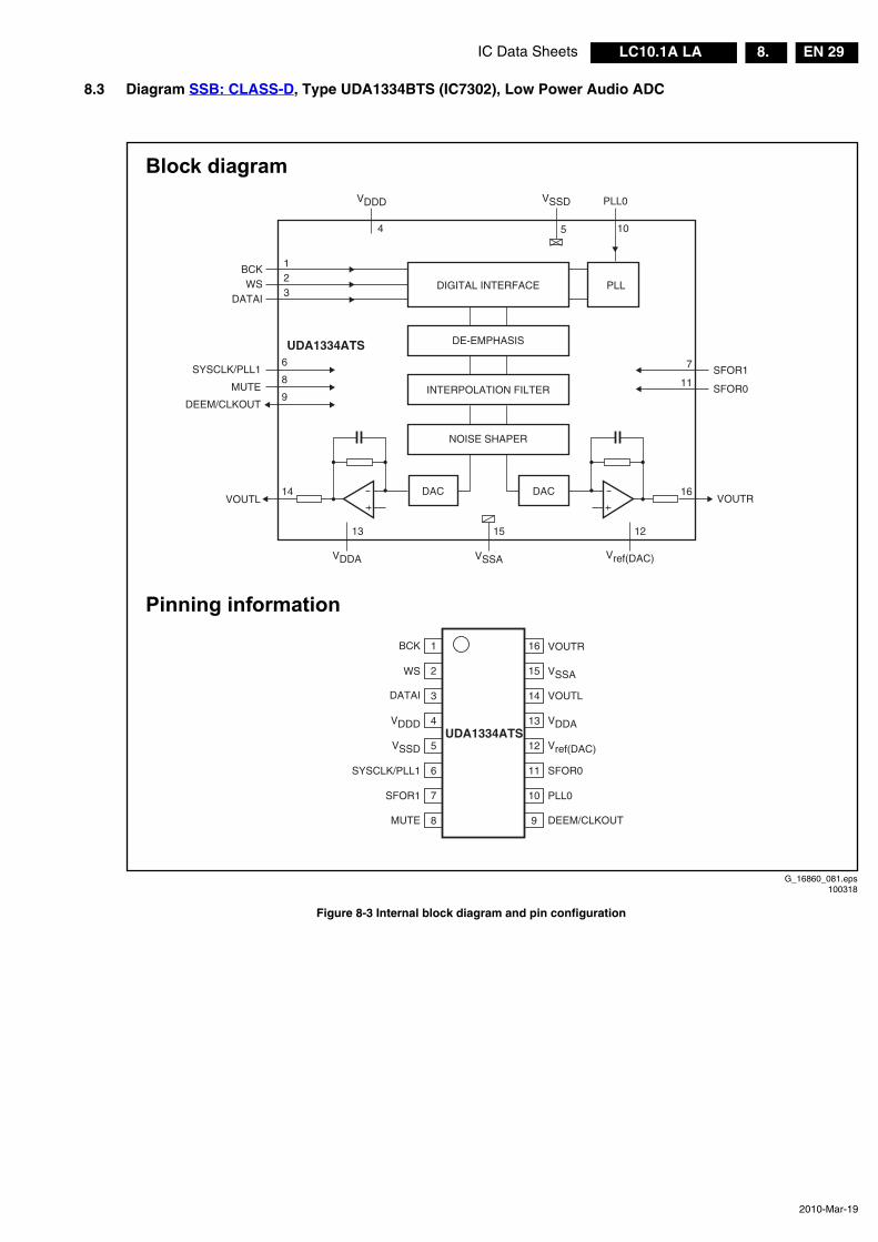
8.3 Diagram SSB: CLASS-D, Type UDA1334BTS (IC7302), Low Power Audio ADC
Figure 8-3 Internal block diagram and pin configuration
G_16860_081.eps100318
Block diagram
Pinning information
UDA1334ATS
1
2
3
4
5
6
7
8
16
15
14
13
12
11
10
9
VOUTRBCK
VSSAWS
VOUTLDATAI
VDDAVDDD
Vref(DAC)VSSD
SFOR0SYSCLK/PLL1
PLL0SFOR1
DEEM/CLKOUTMUTE
DAC
UDA1334ATS
NOISE SHAPER
INTERPOLATION FILTER
DE-EMPHASIS
14
15
DAC
6
DIGITAL INTERFACE PLL
16
321
4 5
11
7
13 12
VOUTR
BCK
VSSA
WS
VOUTL
DATAI
VDDA
VDDD
10
PLL0
Vref(DAC)
VSSD
SFOR0
SYSCLK/PLL18
MUTE9
DEEM/CLKOUT
SFOR1

IC Data SheetsEN 30 LC10.1A LA8.
2010-Mar-19
8.4 Diagram SSB: Power MT MT8222, Type MT8222 (IC7A00), Video/Audio System-on-Chip (SoC)
Figure 8-4 Internal block diagram
18870_300_100211.eps100305
Block diagram
CVBS / SV (8 ×)
Analog Front End
ADC 3D TVD 8032
Main Path (Customer) External Switches
YPbPr (2 ×)
VGA
ADC
ADC
ADC
HDTVD
VGAD
MDDi
PIP Path
DS
HDMIx3
Digital Path
MDDi DS
OSD
Control Signal (GPIO,...)
LVDS LVDS Tx
Merge
Gamma
Dithering
Color
Color
US
US
DSP
DR
AM
MU X

IC Data Sheets EN 31LC10.1A LA 8.
2010-Mar-19
8.5 Diagram SSB: Power MT MT8222, Type MT8222 (IC7A00), Video/Audio System-on-Chip (SoC)
Figure 8-5 Pin configuration
18870_301_100211.eps100305
Pinning information
IC Data SheetsEN 32 LC10.1A LA8.
2010-Mar-19
8.6 Diagram SSB: Stand-by, Type WT61P7 (IC7D00), Standby Processor
Figure 8-6 Internal block diagram and pin configuration
I_18170_024.eps100319
Block diagram
Pinning information
61P8S_RG480WT(LQFP)
38
36
35
34
33
32
31
30
29
28
27
26
1
2
3
4
5
6
7
8
9
10
11
VDD33V
GND
OSCO
OSCI
13 14 15 16 17 18 19 20 21 22 23
39404142434445464748
12 25
2437
NC1
NC5
NC2
NC3
61P8S_RG440WT(LQFP)
34
3332
31
30
29
28
27
26
25
24
23
GPIOD2/P10/AD4GPIOD3/P11/AD5
GPIOD4/P12/AD6
GPIOD5/P13/AD7
GPIOD6/TXD1
GPIOD7/RXD1
GPIOA0/PWM4/P00GPIOA1/PWM5/P01
GPIOA2/PWM6/P02
GPIOA3/PWM7/P03
GPIOA4/DSCL2
12
3
4
5
6
7
8
9
10
11
VDD33VGND
OSCO
OSCI
GPIOB6/SSDA
GPIOB5/SSCL
GPIOB4/P05
GPIOB3/P04
GPIOB2/IR
GPIOB1/IRQ3/CEC
GPIOB0/IRQ2
GPIOC7/P1
7/IRQ1
GPIOC6/P1
6/IRQ0
GPIOC5/P1
5/TX
D0
GPIOC4/P1
4/RX
D0
GPIOC3/AD3
12 13 14 15 16 17 18 19 20 21 22GPIOA5/DSD
A2
DSC
L1
DSD
A1
GPIOC0/AD0
GPIOC1/AD1
GPIOC2/AD2
35363738394041424344
GPIOD0/HIN1
GPIOE7
/VIN1
GPIOD1/HIN2
GPIOE6
/VIN2
GPIOE1
/PWM1
NRS
T
GPIOE0
/PWM0
GPIOE2
/PWM2
GPIOE3
/PWM3
GPIOE4
/LPW
M/P06
GPIOE5
/P07
GPIOB6/SSDA
GPIOB5/SSCL
GPIOB4/P05
GPIOB3/P04
GPIOB2/IR
GPIOB1/IRQ3/CEC
GPIOB0/IRQ2
GPIOC7/P1
7/IRQ1
GPIOC6/P1
6/IRQ0
GPIOC5/P1
5/TX
D0
GPIOC4/P1
4/RX
D0
GPIOC3/AD3
GPIOA5/DSDA2
DSC
L1
DSD
A1
GPIOC0/AD0
GPIOC1/AD1
GPIOC2/AD2
GPIOD2/P10/AD4
GPIOD3/P11/AD5
GPIOD4/P12/AD6
GPIOD5/P13/AD7
GPIOD6/TXD1
GPIOD7/RXD1
GPIOA0/PWM4/P00
GPIOA1/PWM5/P01
GPIOA2/PWM6/P02
GPIOA3/PWM7/P03
GPIOA4/DSCL2
GPIOD0/HIN1
GPIOE7
/VIN1
GPIOD1/HIN2
GPIOE6
/VIN2
GPIOE1
/PWM1
NRS
T
GPIOE0
/PWM0
GPIOE3
/PWM3
GPIOE4
/LPW
M/P06
GPIOE5
/P07
GPIOE2
/PWM2
Turbo 8052 MCU
Key Pad ADC
RTC
Timer0,Timer1,Timer2,Timer3,UART0,UART1
VGA DDC
Slave IIC
PWM/LPWM
InterruptProcessor
4 IRQProcessor
1 HV Synccounter
Watchdogtimer
ResetProcessor
ClockProcessor
Clock off &Wake Up
GPIOProcessor
IR Detector
32K bytescode flash
Internal 256bytes SRAM
inte
rnal
bus
DVI DDC
2 HV Synccounter
CEC
External 512Kbytes SRAM
IC Data Sheets EN 33LC10.1A LA 8.
2010-Mar-19
8.7 Diagram SSB: I/Os Audio, Type TPA6111A2DGN (IC7F00), Stereo Audio Power Amplifier
Figure 8-7 Internal block diagram and pin configuration
18770_309_100217.eps100217
Block diagram
Pinning information
BiasControl
8
1
7
4
VO1
VO2
VDD
5
2
3
6
IN1−
BYPASS
SHUTDOWN
VDD/2
IN2−
−+
−+
1234
8765
VO1IN1−
BYPASSGND
VDDVO2IN2−SHUTDOWN
D OR DGN PACKAGE(TOP VIEW)
IC Data SheetsEN 34 LC10.1A LA8.
2010-Mar-19
8.8 Diagram SSB: TCON DC/DC, Type ISL97653A (IC7KFA), 5-channel Integrated LCD Supply
Figure 8-8 Internal block diagram and pin configuration
18770_307_100217.eps100217
Block diagram
Pinning information
1
40
2
3
4
5
6
7
8
9
10
30
29
28
27
26
25
24
23
22
21
39 38 37 36 35 34 33 32 31
11 12 13 14 15 16 17 18 19 20
LDO
-CTL
LDO
-FB
PVIN
1
AG
ND
PRO
T
LX2
LX1
PGN
D2
PGN
D1
TEM
P
COMP
FBB
RSET
HVS
EN
CDEL
CTL
DRN
COM
POUT
PVIN2
CB
LXL1
LXL2
PGND3
PGND4
CM2
FBL
VL
VREF
FBN
SUPN
NO
UT
PGN
D5
C1P
C1N C2P
C2N
SUPP FB
P
ISL97653A40 LD 6X6 QFN
TOP VIEW
+-
+-
+-
+-
+-
+-
+-
+-
Ε
Ε
CONTROLLOGIC
SAWTOOTHGENERATOR
CURRENTAMPLIFIER
CURRENT LIMITCOMPARATOR
CURRENT LIMITTHRESHOLD
REFERENCE BIAS
AND
SEQUENCE CONTROLLER
VREF
GM AMPLIFIER
UVLO COMPARATOR
OSCILLATOR
0.75 VREF
REGULATOR
SUPN
0.2V
UVLO COMPARATOR
0.4V
0.75 VREF
VREF
POUT
RSENSE
BUFFER
CONTROLLOGIC
VREF
SAWTOOTHGENERATOR
SLOPECOMPENSATION
GM AMPLIFIER
SUPP
CURRENT LIMITTHRESHOLD
CURRENTLIMIT
COMPARATOR
SUPP
C1- C1+ C2+ C2-POUT CTL COM
BUFFER
LX1
PGND1
CB
LXL1
CM2
FBL
FBP
FBN
NOUT
PVIN1,2
EN
CDEL
PVIN1,2
VL
FBB
CM1
PGND2
LX2
CURRENT AMPLIFIER
SLOPECOMPENSATION
VREF
FREQ
HVSLOGIC
RSET HVS PROT
LXL2
DRN
680kHz
VL
LDOCONTROL
LOGIC2
LDO-CTL
LDO-FB
TEMPSENSOR TEMP
Block Diagrams EN 35LC10.1A LA 9.
2010-Mar-19
9. Block Diagrams
Wiring Diagram 42" - 46" (van Gogh)
TWEETER(5216)
TWEETER(5216)
MAINSSWITCH
(8311)
11P
1M95
9P
1M99
2P3
1311
2P3
1308
1735
4P
1M95
11P
1319
32"-
6P
1316
32"-
12P
1319
40"-
10P
46"-
10P
1316
40"-
10P
46"-
10P
1M99
9P
1KA2
80P
1KA1
80P
1M20
8PM
AIN
S C
OR
D
8191
TO DISPLAY TO DISPLAY
3P J1
SSB(1150)B
MAIN POWER SUPPLY32"- DPS-138BP A B 40"- DPS-206CP A B46"- FSP173-3MS01 B(1005)
LCD DISPLAY(1004)
KE
YB
OA
RD
CO
NT
RO
L(1
114)
IR / LED BOARD (1112)
8M99
8M95
8311
WIRING DIAGRAM 32"- 46" VAN GOGH
18920_400_100318.eps100319
1M99 (B01)1. +12VDISP2. +12VDISP3. GND4. GND5. BL_ON_OFF6. PWM_DIMMING7. BACKLIGHT_BOOST8. GND9. POWER_OK
1M95 (B01)1. +3V3STDBY2. STANDBY3. GND4. GND5. GND6. +12VS7. +12VS8. +12VS9. +24VAUDIO10. GNDSND11. N.C. 1735 (B03)
1. LEFT_SPEAKER2. GNDSND3. GNDSND4. RIGHT_SPEAKER
1M20 (B04C)1. LIGHT_SENSOR2. GND3. IR4. LED25. +3V3STBY6. LED17. KEYBOARD8. +5V_SW
1KA2 (B08E)1. GND| 11. VLS_15V612. VLS_15V6| 33. VCC_3V334. VCC_3V3|78. VGH_35V79. VGL_-6V80. GND
1KA1 (B08E)1. GND| 11. VLS_15V612. VLS_15V6| 33. VCC_3V334. VCC_3V3|78. VGH_35V79. VGL_-6V80. GND
LN
Board Level Repair
Component Level RepairOnly For Authorized Workshop
USB
HD
MI
TUN
ER
PHO
NE
SPD
IF
HDMIHDMIVGA
LOUDSPEAKER(5213)
8M20
TO B
AC
KLI
GH
T
8KA2
NOT FOR 32" TV-SETS NOT FOR 32" TV-SETS J2
3P
J1
8P
8KA1
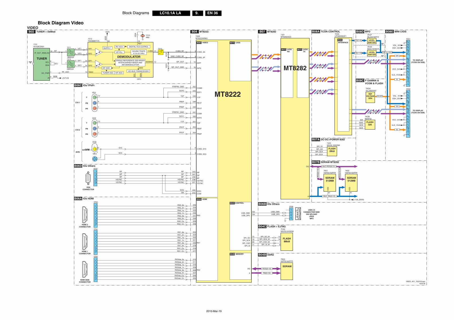
EN 36LC10.1A LA 9.Block Diagrams
2010-Mar-19
Block Diagram Video
B02 TUNER + DeMod B07 MT8282 B08A TCON CONTROL
B08C P GAMMA &VCOM & FLASH
B08D MPD B08E MINI LVDS
B07A DC-DC+POWER 8282
B04 MT8222:
B06C IOs YPbPr
B06D IOs Others
B04C FLASH + EJTAG
B04B DDR2
B06B IOs Others
B06A IOs HDMI
B07B SDRAM MT8282
7KUFISL24016IRTZ
1E01
7A00MT8222ARMU
LVDSB07CVIDEOB06C
Y0P
SOY0
YPBPR0_GND
PB0P
PR0P
PB
PR
Y
PB
PR
Y
248
246
245
MT8222
7C00MX25L6445EMI
FLASH8Mx8
18920_401_100318.eps100318
VIDEO
7
12
9
CVBS_0N
CVBS_0P
1
5SVHS IN
24
3
1E10
1E08
CVBSSY0
SC0
4
3
2CVBS_SY0
CVBS_SC0
249PR1P
Y1P
SOY1
252COM0
PB1P
1
1E05
2
3
14
13
RP
GP
SOG
GN
BP
HSYNC
VSYNC
HSYNC
VSYNC
RP
GP
BP
1 610
11
5
15
VGACONNECTOR
237
238
239
242
240
241
243 RP
VSYNC
GP
BP
HSYNC
SOG
COM
SPI_SO_MSPI_SCK_M
70 15
1672SPI_CSO_M
SPI_SI_M69 7
871
SPI_SCKSPI_SO
SPI_CSOSPI_SI
1E02
Y1P
SOY1
PB1P
PR1P
253
251
250
7
12
9
254PR0P
Y0P
SOY0
PB0P
14
5
1211
SIF1
SIF2
VIF1
VIF2
1
217CVBS
DEMODULATOR
7212TDA9885T/V5
AIF
+5VTUN
1T01VA1E8CD501
TUNER
12IF_OUT_ANALOG
CVBS_RF
GND_CVBS_RF
9
8
SOUND TRAPS4.5 to 6.5 Mhz
VIF-PLL
SINGLE REFERENCE QSS MIXERINTERCARRIER MIXER AND
AM-DEMODULATOR
TUNER AGC VIF AGCTAGC
SIF AGC
I2C-BUS TRANSCEIVER
MAD
SC
L
SD
A
SUPPLY
+5VS
1 RF_AGCDC_PWR
8+B
DIDITAL VCO COTROLRC VCO
REF
38MHz9
20
(I2C)
15
4
1212
38MHz9
15
12134M0
23
24
14
12SIOMAD SIF_OUT
SIF_OUT_GND
EF7213
2215
2209
2223
5208
VIF1
VIF2
SIF1
SIF2
5203
SCL
SDA7
6(I2C)
SDRAM
7B00H5PS5162FFR
MEMORYB04B
DQ
A
RDQ(0-15)
RA(0-12)
43
21
USB_DM0USB_DP0
USB 2.0CONNECTOR SIDE
SW UPLOADJPEGMP3
193
194USB_DP0USB_DM0
1P081
2
4
3
CONTROLB04C
SIFP
SIFN
14
15
HDMIB06A
RX0
RX1
RX2
235
234
229
258
233
232
231
230
224
223
218
217
222
221
220
219
191
182
1
1P03
3
4
7
910
12
6
RX2_2p
RX2_2n
RX2_1p
RX2_1n
RX2_0p
RX2_0n
RX2_Cp
RX2_Cn
RX1_2p
RX1_2n
RX1_1p
RX1_1n
RX1_0p
RX1_0n
RX1_Cp
RX1_Cn
HDMI 2CONNECTOR
1
1P02
3
4
7
910
12
6
1
1P05
3
4
7
910
12
6
191
182
HDMI 1CONNECTOR
191
182
HDMI SIDECONNECTOR
RXSide_2p
RXSide_2n
RXSide_1p
RXSide_1n
RXSide_0p
RXSide_0n
RXSide_Cp
RXSide_Cn
212
211
206
205
210
209
208
207
E
O
PX1
PX2
TO DISPLAY(TCON ON SSB)
TO DISPLAY(TCON ON SSB)
1KA2
72
81
61
50
13
33
34
12
11
1KA181
72
79
78
61
2
10
1
1
7J01MT8282AGG
7KAAUPD809900F1
7KQAISL24837IRZ
VL/VH
VH
REFVOLTAGE
GEN
7KUEMAX17079GTL
LEVELSHIFTER
LEVELSHIFTER
CS(1U-12U)CS(1-12)
CS(1-6)
VLS_15V6
VCC_3V3
12
11VLS_15V6
7J03MX25L1605DMI
FLASH2Mx8
SPI_S1
SPI_SOSPI_SC#
SPI_SCK
7KQBM25P32
FLASH32K
SDI
SDOSCS
SCK
VGL_-6V
VGH_35V
2
10
LVDSRX
B07C LVDSTX
B07C
INTERFACEB08A
A1A1
+1V8_DDR2
SDRAM512MB
7K02H5PS5162FFR
DQ
A
SDRAM512MB
7K01H5PS5162FFR
VD
D
VD
D
MJC-RDQ(0-31)
RD
Q(0
-15)
RD
Q(1
6-31
)
MJC_RA(0-12)
PX3
PX4
33
34
VCC_3V3
50
13L_LVx
L_RVx
MT8282
79
78VGL_-6V
VGH_35V
VL
VH
VL
32"
42"
CVI-1
CVI-2
AVIN
YPBPR1_GND 247COM1
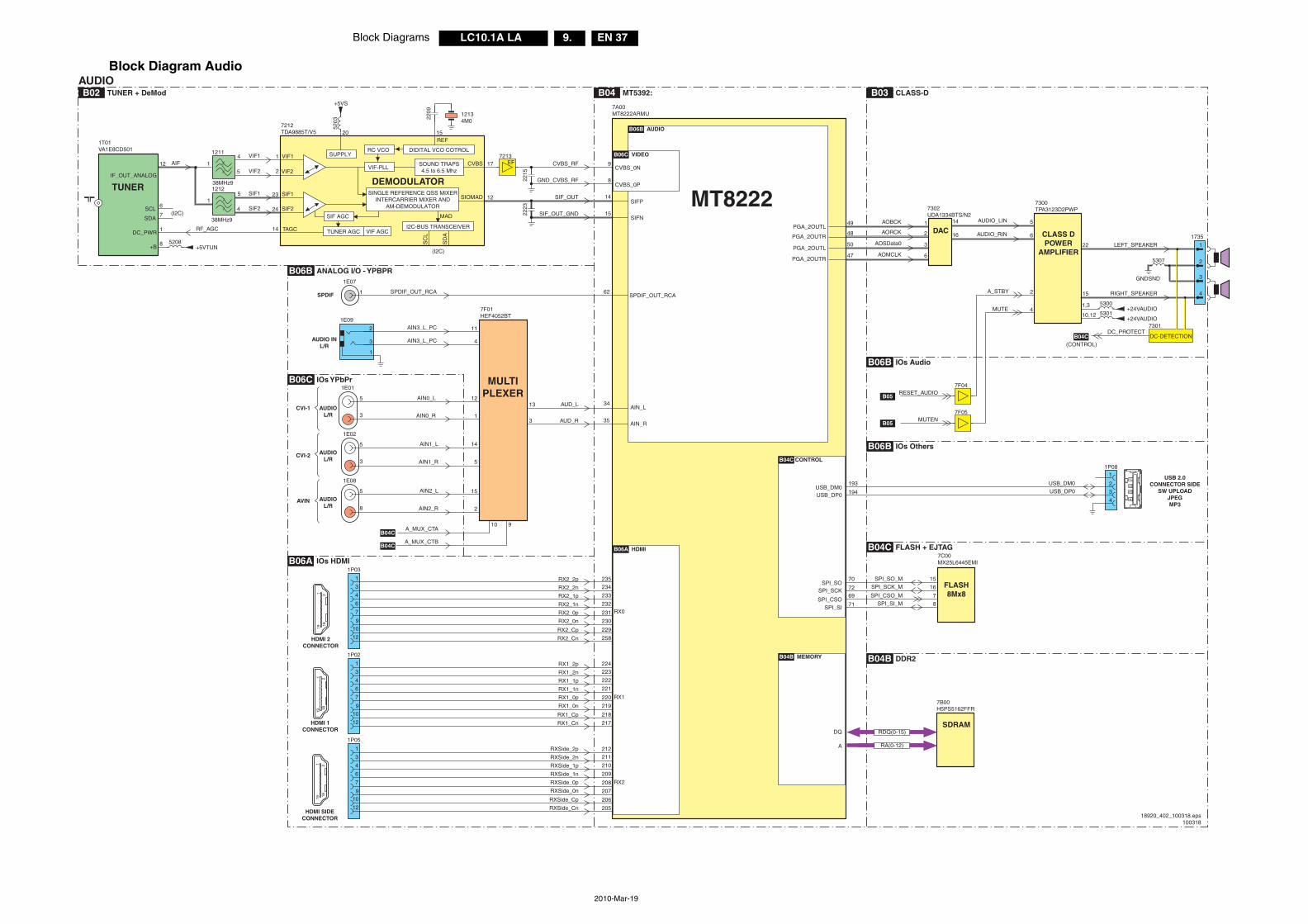
Block Diagrams EN 37LC10.1A LA 9.
2010-Mar-19
Block Diagram Audio
B02 TUNER + DeMod B03 CLASS-DB04 MT5392:
B06A IOs HDMI
B06B ANALOG I/O - YPBPR
B06C IOs YPbPr
B04B DDR2
B06B IOs Audio
B06B IOs Others
B04C FLASH + EJTAG
SDRAM
7B00H5PS5162FFR
7A00MT8222ARMU
AUDIOB06B
HDMIB06A
VIDEOB06C
MEMORYB04B
CONTROLB04C
RX0
RX1
RX2
235
234
229
258
233
232
231
230
224
223
218
217
222
221
220
219
191
182
1
1P03
3
4
7
910
12
6
RX2_2p
RX2_2n
RX2_1p
RX2_1n
RX2_0p
RX2_0n
RX2_Cp
RX2_Cn
RX1_2p
RX1_2n
RX1_1p
RX1_1n
RX1_0p
RX1_0n
RX1_Cp
RX1_Cn
HDMI 2CONNECTOR
1
1P02
3
4
7
910
12
6
1
1P05
3
4
7
910
12
6
191
182
HDMI 1CONNECTOR
191
182
HDMI SIDECONNECTOR
MT8222
18920_402_100318.eps100318
43
21
USB_DM0USB_DP0
USB 2.0CONNECTOR SIDE
SW UPLOADJPEGMP3
193
194
AUDIO
CVBS_0N
CVBS_0P
SIFP
SIFN
USB_DP0USB_DM0
DQ
A
1P081
2
4
3
1E09
2
3
1
SPDIF_OUT_RCA
AIN3_L_PC
AIN3_L_PC
1E07
SPDIF
34
35
AIN_L
62
11
4
12
1
14
5
15
2
SPDIF_OUT_RCA
AIN_R
1E01
AUDIO INL/R
AIN0_R
AIN0_L
1
AUD_R
AUD_L
AIN1_L
AIN1_R
1E02
AUDIOL/R
5
3
AIN2_L
A_MUX_CTA
A_MUX_CTB
AIN2_R
1E08
AUDIOL/R
AUDIOL/R
CVI-1
CVI-2
AVIN
5
8
5
3
49
48PGA_2OUTL
PGA_2OUTR50
47PGA_2OUTL
PGA_2OUTR
AUDIO_LIN
AUDIO_RIN
LEFT_SPEAKER
RIGHT_SPEAKER
GNDSND
7300TPA3123D2PWP
CLASS DPOWER
AMPLIFIER
7302UDA1334BTS/N2
DAC5
6AOSData0
AOMCLK
3
6
22
15
MUTE
MUTEN
4
1
2
1735
3
4
DC-DETECTION
A_STBY 2
B05
B05
DC_PROTECTB04C
7301
(CONTROL)
14
5
1211
SIF1
SIF2
VIF1
VIF2
1
217CVBS
DEMODULATOR
7212TDA9885T/V5
AIF
+5VTUN
1T01VA1E8CD501
TUNER
12
IF_OUT_ANALOG
CVBS_RF
GND_CVBS_RF
9
8
SOUND TRAPS4.5 to 6.5 Mhz
VIF-PLL
SINGLE REFERENCE QSS MIXERINTERCARRIER MIXER AND
AM-DEMODULATOR
TUNER AGC VIF AGCTAGC
SIF AGC
I2C-BUS TRANSCEIVER
MAD
SC
L
SD
A
SCL
SDA
SUPPLY
+5VS
1
7
6
RF_AGCDC_PWR
8+B
DIDITAL VCO COTROLRC VCO
REF
38MHz9
20
(I2C)
(I2C)
15
4
1212
38MHz9
15
12134M0
23
24
14
12SIOMAD SIF_OUT
SIF_OUT_GND
14
15
EF7213
2215
2209
2223
5208
VIF1
VIF2
SIF1
SIF2
5203
5307
+24VAUDIO1,3 5300
+24VAUDIO10,12 5301
AOBCK
AORCK
1
2
14
16
RDQ(0-15)
RA(0-12)
7C00MX25L6445EMI
FLASH8Mx8
SPI_SO_MSPI_SCK_M
70 15
1672SPI_CSO_M
SPI_SI_M69 7
871
SPI_SCKSPI_SO
SPI_CSOSPI_SI
RXSide_2p
RXSide_2n
RXSide_1p
RXSide_1n
RXSide_0p
RXSide_0n
RXSide_Cp
RXSide_Cn
212
211
206
205
210
209
208
207
7F05
RESET_AUDIO7F04
7F01HEF4052BT
MULTIPLEXER
13
10 9
3
B04C
B04C

EN 38LC10.1A LA 9.Block Diagrams
2010-Mar-19
Block Diagram Control & Clock SignalsCONTROL + CLOCK SIGNALS
B04B DDR2B04 MT8222
B04C FLASH & EJTAG
B06E IOs HDMI
B04C FLASH & EJTAG
B05 StANDBY
B06H IOs Others
B07A DC-DC+POWER 8282
B04C FLASH & EJTAG
B01 DC-DC
B07A DC-DC+POWER 8282
B07B SDRAM MT8282
1M20
3
7
6
4
8
5
+5V_SW
+3V3STBY
+3V3_SW
MT8222
7A00MT8222ARMU/B
7D00WT61P7-RG480WT
76
77UART
SERVICECONNECTOR
UART_RX
UART_TX
3
2
1
GPIO2
GPIO6
119
123
68
INTO74 POWER_DOWN
PWM_0
RXD0
TXD0
63 Boost_Control BACKLIGHT_BOOST
2C29
SDM2C28
PANEL
MT8222_RST
7C01BD45292G
VOUT
VDD
18490_403_100318.eps100318
SDRAM
7B00H5PS5162FFRMEMORYB04B
HDMIB06E
CONTROLB04C
DQ
A
CK
CK
RDQ(0-15)
RA(0-12)
J8RCLK0163
K8RCLK0#162
54
3
3C24
PWM_1 64 Backlight_Control PWM_DIMMINGPWMDIMMING
PWM_2 65B04C
SYS_EEPROM_WE
PWM_3 66B06F
A_MUX_CTB
UP3_0 78B06E
HDMI_HPD_1
UP3_1 79B04C
MAINFLASH_WP
UP3_3 80B06E
HDMI_HPD_2
UP3_5 82B06E
HDMI_HPD_SIDE
GPIO0117 INT_CEC
GPIO1 118B07C
LCD_PWR_ON
GPIO4 121 MJC_RXDMA_ACK
GPIO5 122 MJC_RXDMA_COMM
GPIO7 124B03
DC_PROTECT
GPIO9 126 USB_PWE
GPIO8 125 POWER_OK
GPIO21 53 BL_ON_OFF
GPIOE_2 44 STANDBY
GPIO22 54B06F
A_MUX_CTA
GPIO22 55B06F
CTRL-DISPBYPASSn
IR_1
GPIO22 55B06E B06H
EDID_WE
GPIO25 57 Muten_2
7C08
Boost_Control
18ADIN_0
KEYBOARD
1
2
21ADIN_3
LIGHT_SENSOR
75IR
IR
CLK0
29 GPIOA_1
21 GPIOC_0
10 GPIOB_2
GPIOB_1
7 GPIOB_5
38 GPIOD_0
A7 MJC_CLK0#CLK0
OSC_I
OSC_O
B7
5
4
MJC_CLK0
CLK1P1 MJC_CLK1#
CLK1P2 MJC_CLK1
27
11
LED1
LED2GPIOA_2
GPIOA_3
28
7C13
+3V3_SW
STANDBY
1D0312M
XTAL_I
XTAL_O
W19
W20
RXDMA_ACKW1
GPIO3 120 MJC_RST#PRST
W2
GPIO_2W3
1J0127M
43
21
USB20-DM0USB_DM0
193
USB_DP0194 USB20-DP0
USB 2.0CONNECTOR
SIDE
1P08
3
4
2
15V
7H01TPS2041BD
EN
OUTGPIO10 127 USB_OC
OC
7H04
5
4
6,7,8
7C00MX25L6445EMI
FLASH8Mx8
SPI_SO_MSPI_SCK_M
70 15
1672SPI_CSO_M
SPI_SI_M69 7
871
SPI_SCKSPI_SO
SPI_CSOSPI_SI
201CEC
CEC_HDMI_8222B06E
CEC CEC_HDMI_SOC4E00 4E01
7J01MT8282AGG
7J03MX25L1605DMI
FLASH2Mx8
SPI_S1
SPI_SOSPI_SC#
SPI_SCK
J8 K8 J8 K8
15
8
7
16
SDRAM512MB
7K02H5PS5162FFR
DQ
Q
DS
C
A
SDRAM512MB
7K01H5PS5162FFR
MJC-RDQ(0-31)
RD
Q(0
-15)
RD
Q(1
6-31
)
MJC_RA(0-12)
MT8282
TO IR/LED BOARD &KEBOARD CONTROL
1M99
6
7
1M952
5
9TO IR/LED BOARD &KEBOARD CONTROL

Block Diagrams EN 39LC10.1A LA 9.
2010-Mar-19
Block Diagram I2CI²C
HDMI & MUXB05
TCON CONTROLB08A P GAMMA & VCOM & FLASHB08C
DC-DC + POWER 8282 B07A SDRAM MT8282B07B
IOs OthersB06D
TUNER + DeModB02FLASH + EJTAGB04C
IOs HDMIB06A
FLASH + EJTAGB04
DDR2B04B
1KQB
DEBUG ONLYRES
4
2
1
7A00MT8222ARMU/B
HW_SDA
HW_SCL
PWM_2
CONTROL
65 7
V3
Y3
59
58 TUNER_SDA
TUNER_SCL
SYS_EEPROM_WE
SDA
SCL
STBY_SDA
STBY_SCL
3218
3219
+3V3_SW
3C62
3C61
+3V3_SW
UA0RX
UA0TX
18920_404_100318.eps100318
10 11
7212TDA9885T/V5
DEMODULATOR
3213
3212
7 6
1T01VA1E8CD501
MAINTUNER
5 6
7C04M24C64
EEPROM(NVM)
3C67
3C66
76
77
UART_RX
UART_TX
U2RX
U2TX
3C01
3C02
3C35
3C36
+3V3STBY
UARTSERVICE
CONNECTOR
3C38
3C37
1E06
3
2
1
ERR34
ERR27
B04C
ERR35
U11 V11
7J01MT8282AGG
PHERIPHERAL
3J15
3J14
ERR21 22 23
7D00WT61P7
STANDBY
3D04
3D03
7C09
1 610
11
5
15
VGACONNECTOR
VGA-SDA-EDID-TCON
VGA-SCL-EDID-TCON
1E05
12
15
3H29
3H30
DC_5V
3KT
U
3KT
V
VCC_3V3
BYPASS_MODE
5 6
7H02M24C02
EEPROM
4H03
4H02
7EDID_WE7H03
B04C
MT8222
+3V3_SW
SDA
SCL
4D04
4D03
SDA-TCON
SCL-TCON
E19 E20
K21
K20 1
27KAA
UPD809900F1
CONTROL
12 13
7KQAISL24837IRZ
VOLTAGEGENERATOR
7 8
7KQHPCA9540BDP
I2CSWITCH
HDMICONNECTOR
SIDE
HDMICONNECTOR 2
1P03
16
15
3E04
3E05
3E01
3E02
+5VHDMI_2
226
227
HDMICONNECTOR 1
1P02
16
15
3E18
3E19
3E14
3E15
+5VHDMI_1
214
215
1P05
16
15
3E30
3E31
3E25
3E26
+5VHDMI_SIDE
203
204
DDC_SDA_HDMI_2
DDC_SCL_HDMI_2
DDC_SDA_HDMI_1
DDC_SCL_HDMI_1
DDC_SDA_SIDE
DDC_SCL_SIDE
3E36
3E35
3E38
3E37
3E40
3E39
2
1
7214
7215
7C00MX25L6445EMI
FLASH8Mx8
SPI_SO_MSPI_SCK_M
70 15
1672SPI_CSO_M
SPI_SI_M69 7
871
60
61
SPI_SCKSPI_SO
SPI_CSOSPI_SI
RXD1
TXD1
SDRAM
7B00H5PS5162FFRMEMORYB04B
HDMIB06A
DQ
HDMI_SDA0
HDMI_SCL0
HDMI_SCL1
HDMI_SCL2
HDMI_SDA1
HDMI_SDA2
A
RDQ(0-15)
RA(0-12)
RDQ(0-15)
RA(0-12)
7E00 M24C02
EEPROM
7E01 M24C02
EEPROM
7E02 M24C02
EEPROM
7KAB LM75BDP
TEMPSENSOR
Programmable via USB
MAINSW
MAIN NVMSW
SW
SW
SW
Programmable via ComPair
Pre-programmed device
EDIDSW
7K01H5PS5162FFR
SDRAM512MB
7K02H5PS5162FFR
7J03MX25L1605DMI
FLASH2Mx8
SPI_S1
SPI_SOSPI_SC#
SPI_SCK
RXD0Y17
W17 RXD0
7KQBM25P32
FLASH32K
SDI
SDOSCS
SCK TCONSW
EDIDSW
EDIDSW
EDIDSW
MT8282SW
3J13
3J07
1J04
DEBUG ONLYRES
3
2
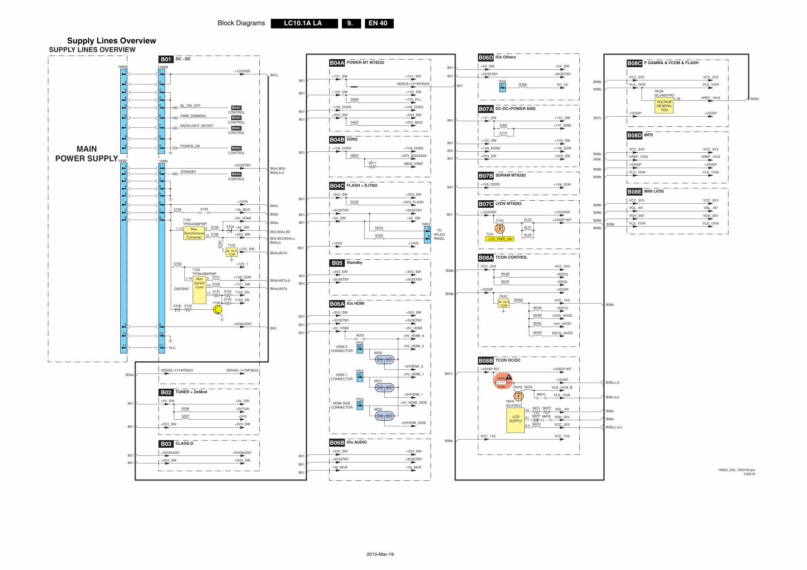
EN 40LC10.1A LA 9.Block Diagrams
2010-Mar-19
Supply Lines Overview SUPPLY LINES OVERVIEW
MAINPOWER SUPPLY
B01 DC - DC
B08A TCON CONTROL
B04C FLASH + EJTAG
B05 Standby
B04A POWER MT MT8222
B04B DDR2
B07B SDRAM MT8282
B06A IOs HDMI
B06D IOs Others
B07A DC-DC+POWER 8282
B07C LVDS MT8282
B08C P GAMMA & VCOM & FLASH
B08D MPD
B08E MINI LVDS
B02 TUNER + DeMod
B03 CLASS-D B06B IOs AUDIO
B08B TCON DC/DC
1M99
1 1
6 6
7 7
8 8
1M95+3V3STBY
18920_405_100318.eps100318
B07c
B04c
B04c,B05,B06a,b,d
B06b
B06a
B02,B04c,B2
B04a,B07a
B02,B03,B04a,cB06a,b
B04a,B07a,b
B04a,B07a
B03
1M99
1 1
6 6
7 7
2 2
3 3
4 4
5 5
8 8
BL_ON_OFF
1M99
BACKLIGHT_BOOST
+12VDISP
PWM_DIMMING B04C
B04C
+12VS
+Va_MUX
9 9 +24VAUDIO
10 10
+5V_SW
+5V_HDMI
+3V3_SW
+1V2_SW
+12V_1
CONTROL
CONTROL
B04CCONTROL
B06DCONTROL
9 9 POWER_OK
2 2
3 3
4 4
5 5
STANDBY
GNDSND
B04ACONTROL
11 11
7103TPS54386PWP
NonSynchronous
Converter
+3V3_SW+3V3_SW
+3V3STBY+3V3STBYB01
B01
N.C.
5104
5109
+1V8_DDR+1V8_DDR2B01
5J14
+1V1_SW+1V1_SW
+1V8_DDR+1V8_DDR2
+3V3_SW+3V3_SW
+1V2_SW+1V2_SW
5J02 +1V1_8282B01
B01
B01
+5V_HDMI_2
+3V3STBY+3V3STBY
+3V3_SW+3V3_SW
+5VHDMI_2
1P0318HDMI 2
CONNECTOR
B01
B01+5V_HDMI+5V_HDMI
+5V_HDMI_AB01
5106
5100
31,14
12
+1V8_DDR
+1V1_SW
7102TPS54386PWP
NonSynchrConv
5101
5102
31,14
12
11
VCC_3V3VCC_3V3B08b
+VDISP+VDISPB08b
VDDQ5KAF
VDD335KAE
SSCG_AVDD5KAD
mini_AVDD5KAC
LVDS_AVDD5KAB
VDD125KAA
+1V1_SW+1V1_SW
B01+3V3_SW
+3V3_8222
+3V3_SW
B01+3V3_SW+3V3_SW
B01+3V3STBY+3V3STBY
B01+5V_SW+5V_SW
B01 +1V2_SW+1V2_SW
B01
B01+1V8_DDR2+1V8_DDR2
SENCE+1V1MT8222
+3V3_FLASH
B01+1V8_DDR2+1V8_DDR2
5C02
+1V2_PLL5A00
5A02
+3V3_82225A02
MEM_VREF
5B00
1M20
8
5 TOIR/LEDPANEL
5C04
5C05
+12VS+12VSB01
B01
6104
6105
B04aSENSE+1V1MT8222SENSE+1V1MT8222
4100
7102_EN
7103_EN
7105
IN OUTCOM
5104
3131 3132
31357106
3133
3B11
6E00
+3V3STBY+3V3STBY
+5V_SW+5V_SWB01
B01
DC_5V
+5V_HDMI_1
+5VHDMI_1
1P0218HDMI 1
CONNECTOR 6E01
+5V_HDMI_SIDE
+5VHDMI_SIDE
1P0318HDMI SIDE
CONNECTOR 6E02
4E03
+VDISP-INT
VCC_1V2
+12VDISP+12VDISP
7L01LCD_PWR_ON
7L00
B01
5L00
5L01
5L02
1,32
7KAC
IN OUTCOM
5KAG
VREF_15V2
7KQAISL24837IRZ
VOLTAGEGENERA-
TOR+VDISP+VDISP
B07c
B08d
VCC_3V3VCC_3V3B08b
VLS_15V6VLS_15V6B08b
VLS_15V6VLS_15V6B08b
+VDISP+VDISPB08b
VCC_3V3VCC_3V3B08b
VREF_15V2VREF_15V2B08c
VLS_15V6VLS_15V6B08b
B08a,c,d
B08b
B08a,c,d,e
B08c,d,e
B08e
B08e
VGH_35VVGH_35VB08b
B08b
VCC_3V3VCC_3V3B08b
VGL_-6VVGL_-6VB08b
+5V_SW+5V_SWB01
+3V3_SW+3V3_SWB01
+5VS5207
+5VTUN5206
+24VAUDIO+24VAUDIO
+3V3_SW+3V3_SWB01
B01+3V3STBY+3V3STBY
+3V3_SW+3V3_SWB01
B01+Va_MUX+Va_MUX
B01
+VDISP
VLS_15V6_B
VLS_15V6
+VDISP-INT+VDISP-INT
7KFAISL97653
10
21
B07c
VCC_1V2VCC_1V2B08a
1KFA
3.0A 5KFA7KFE
VGL_-6V3KFJ 3KFP
VGH_35V
3,4 VCC_3V35KFD
6KFF 9KFE
9KFC
LCDSUPPLY
1E059 5H06
B01
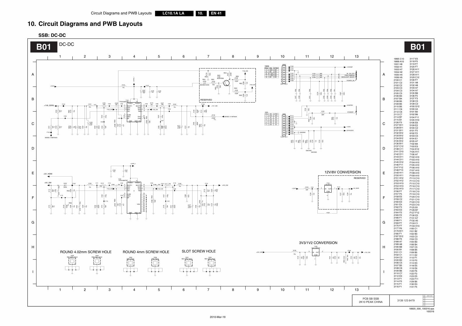
Circuit Diagrams and PWB Layouts EN 41LC10.1A LA 10.
2010-Mar-19
10. Circuit Diagrams and PWB Layouts
SSB: DC-DC
18920_500_100316.eps100316
DC-DCB01 B01
2009-12-301
3139 123 6479PCB SB SSB
2K10 PEAK CHINA
PVDD1 PVDD2
EN1SW1BOOT1
SW2
FB2EN2
BOOT2
FB1
ILIM2SEQBP
GND GND_HS
VIA2VIA1
COM
OUTIN
PVDD1 PVDD2
EN1SW1BOOT1
SW2
FB2EN2
BOOT2
FB1
ILIM2SEQBP
GND GND_HS
VIA2
COM
OUTIN
F118 C10
I103 C3
F120 C10
I105 B3
F122 C10
2
12V
1M99
I123 E5I124 F11I129 B5I130 E3I131 F5
3V
ON
>1.5V
78 12V
I104 C3
25V
I106 B4I107 C5I108 B5I109 B5I111 E2I112 F1I113 F3I114 E3I118 E5I119 E6I120 F6I122 F3
7
12V
ROUND 4.02mm SCREW HOLE
F115 C10F116 C10F117 C10
0V
F119 C10
F121 C10
5106 E6
F123 C10F125 B1F126 B7F127 F12F130 E2F131 E7F132 A5F133 C1F134 H13I100 C1I101 B2I102 B3
12V
3V3
5
0V
3V3/1V2 CONVERSION
F102 A10F103 A10F104 A10F105 A10F106 A10F107 A10F108 A10F109 A10F113 C10F114 C10
0V
STBY
0V
1
3V
0V
ROUND 4mm SCREW HOLE
5105 H10
6
5109 E26100 C26101 F56102 F26103 C56104 E16105 A77102 B47103 E37104 E127105 H117106 A7
1.5V
RESERVED
3V3
3101 C1
3133 A73134 A73135 B83136 F53137 F33138 C53139 C34100 G125100 A45101 B25102 B65104 F11
STBYONPIN
0V
2162 F3
2164 F2
1
2166 F1
3116 F1
3117 E53118 F53119 F73120 F73126 A113127 A113128 A113129 C123130 F73131 A83132 A8
1M95
0V0V
9
PIN
2145 D12
2147 F12
2149 H11
3102 C13104 C33105 B33106 C53107 B53108 C63109 B63110 C73112 E33113 F13114 F33115 F1
SLOT SCREW HOLE
9
0V
0V
2109 B5
2163 E3
2111 C6
2165 F2
2113 C7
2168 F12169 F72170 F72177 F62179 B112180 F12187 B122188 F62189 A72189 A82190 B83100 B1
6
2141 D102142 D112143 D112144 D11
2
2146 F11
4
2148 F13
6
2150 H112151 H122152 H122153 H132154 H132155 H132156 F72157 F52158 E52159 C22160 E32161 E4
2105 C52106 B32107 B42108 B5
B
2110 B5
D
2112 C6
F
2114 B72115 B12126 F32127 B112128 B112131 B112132 B122133 B122134 B122135 B122136 B112137 C12
3V
RESERVED
2138 C11
11 12 13
1 3121110198753
A
B
C
D
E
2102 C22103 C32104 C3
G
H
I
A
12V/8V CONVERSION
C
E
F
G
H
I
1M95 C101M99 A101X01 H61X02 H11X03 H71X04 H21X05 H41X06 H52100 C12101 C2
1 2 3 4 5 6 7 8 9 10
2105
470p
5102
10u
31071R0
RES
1
3
2
BC847BW7106
I102
SS34
6104
I101
100R
3132RES
3131
RES
RE
S
470R
RES
3134
10K
1K0
3133
2168
10p
RES
210633n
210810u
2107
16V100u
F123GNDSND
5101
22u
3109
1%220R
3102
1K2
1%
3100
1%
+1V1_SW
1K8
RES
2116
100n
3113
82K
1%
+5V_SW
RE
S
10p
2100
10u
5106
F114
3112
1R0
1X04REF EMC HOLE
REF EMC HOLE1X03REF EMC HOLE
1X02
REF EMC HOLE1X01
4100
2128
100p
2156
10u
100p
2127
1n0
2141
F116
RE
S
7103_EN
F118
7102_EN
7103_EN 7103_EN
7102_EN 7102_EN
SS
34
6103
3106
10R
I111
33n2110
3116
100K 1%
2188
RES
100n
2190
1u0
1u0
2189
RES
3135
100R
RES
+5V_HDMI
F133
100u
6.3V
2180
RE
S10
p
2170
1%3119
4K7I120
RE
S
2169
10p
I122
I130
BZX384-C6V8
RES
I113
10K
3138
6105
10K
RE
S
RE
S31
39
RE
S31
36
10K
10K
3137
RE
S
RE
S
100n
2143
EMC HOLE1X05
10R
3118
5109
10u
1R031172158 33n
+12VS
10u
2164
6.3V
2101
RE
S
100u
2142
100n
2154
22u
F132
3114
10R
3110
510R1%
F103
I104
I103
I105
I100
+12VDISP
RES 10p
2166
6.3V100u2111
I118I114 I119
2115
10p
RE
S
100p
2134
+1V8_DDR2
F130
4 15
9
1 14
10
213
1617
312
11
6587
+Va_MUX
+3V3_SW
Φ
TPS54386PWP7102
F134
+12VS
10R
3104 21
04
4u7
F126
F131
F125
I112
I123
2177100u6.3V
3108
390R
1X06EMC HOLE
10u2160
33n2163
100u6.3V
2159
1011
23456789
1M95
1-2041145-1
1
10u
2148
2135
10n
I124
7104
2
3 1
L78L08ACU
6101
SS
34
2145
100n
2162
470p
SS
34
6102 4u
7
2126
2113
10p
10p
2114
RE
S
10u
2112
RE
S
F106F107F108
F105
F104
+1V2_SW
18K
3115
1% 2165
6.3V
100u
+3V3STBY
6100
SS
34
3127 68R
3120
1%1K5
2102
10u
1%10K
3101
SENSE+1V1MT8222
10u2109
I106
I107
2103
470p
1n0
2144
+12VS_1
24
2133
100p
16
2526
17181920212223
87
4 15
9
1 14
10
213
7103TPS54386PWP
Φ
312
11
65
100p
2131
2132
100p
100n
2147
F127
+12VS
+12
VS
_1
22u
2152
3130
51K
1%
23456789
2041145-9
1M99
1
F109
2153
RE
S
16V
22u
100n21
51
I129I108
F120
GNDSND
F117
2149
2137
RE
S
22u
1n0
100n
2187
3126 68R
F113
SENSE+1V8MT8222
100n
2136
68R
3129
+3V3_SW10u
5105
GNDSND
2179
100n
68R3128
22u
2138
2146
RE
S
1u0
5104
30R
F122+24VAUDIOF121
2155
2150
22u
100n
F102
F115
216110u
F119
470p
I131
2157
I109
1R03105
1
3 2
LD1117DT127105
5100
10u
POWER_OK
STANDBY
BL_ON_OFFPWM_DIMMING
BACKLIGHT_BOOST
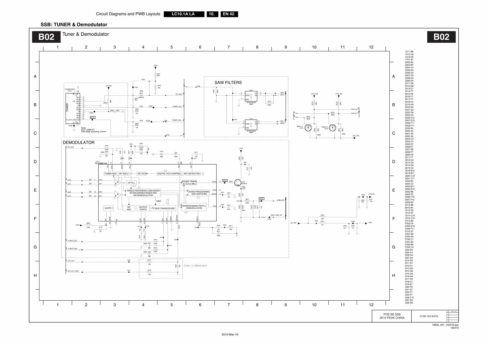
EN 42LC10.1A LA 10.Circuit Diagrams and PWB Layouts
2010-Mar-19
SSB: TUNER & Demodulator
18920_501_100316.eps100319
Tuner & DemodulatorB02 B02
2009-12-301
3139 123 6479PCB SB SSB
2K10 PEAK CHINA
I218 C7I219 E7
A210 B2F203 F8F205 E12
4204 C44205 B114206 B105202 B65203 F2
I229 D8
I213 G5I214 G5
I211 F4I212 F4
2229 F112235 B3
2222 G4
3201 A53202 A53203 C33204 C43205 D73206 E7
3200 A4
F215 E7F227 E8F229 A4F230 C1
I215 G5
3220 C103221 C114203 B4
2211 D6
I220 F6I221 E7I222 F7I223 F7I226 F10
7212 D2
F206 F11
I227 E8
I206 D4I207 D4I210 D6
2227 E122228 F11
2220 G42221 G4
F231 B2F232 B4F233 C4I204 D3I205 C4
3213 G4
I216 G4I217 H4
3219 B11
1212 C81213 D5
2212 D82213 E72214 F72215 F82216 F72217 F7
5206 F105207 F105208 B35212 B86210 B4
7213 E77214 C107215 C10
2205 D32206 D32207 D3
2209 D5
2202 B42203 B42204 C4
2223 H52226 E12
3207 E83208 F73209 F83211 F73212 G4
3214 G43215 H43218 B10
1211 B8
1T01 B1
2218 F32219 G4
2208 D4M
TM
T
TUNER AGC VIF AGC
SUPPLY OUTPUT
VIF-PLL
SINGLE REFERENCE QSS MIXER
AND SWITCHES
DEMODULATORSIFAGC
AFC DETECTOR
PORTS
INTERCARRIER MIXER ANDAM-DEMODULATOR
I C-BUS TRANSCEIVER2
RC VCO
NARROW-BAND FM-PLL
DIGITAL VCO CONTROL
SOUND TRAPS4.5 to 6.5 Mhz
AUDIO PROCESSING
MAD
IO2IGNDO1
GND
IO2IGNDO1
GND
4
2V
H
A
B
SAW FILTERS
DIA 1.2MM FT
TDA9886/V3 0V
2 3 5 6 7 8 9 10
2V2V1
7
2V3
2V1
1 2 4
DEMODULATOR
1V5
12
1
11
D
CTest Keep spaceing 3.5mm
Note:
E
F
G
3
2V
D
8 9 10
H
5 6
2V
11 12
A
B
C
E
F
G
2205
22n
RES
4205RES
I204
3K3
3219
2216
10n
3213
100R
WS_3V3+WS_3V3+
1213
4M0
2222
39p
RES
3221
RES
3K3
3206
1R0
F233
F203
F230
5202
390n
15p
2204RES
F205
+3V3_SW
22u2226
3204
330R
4206RES
100R
3212
470n
2214
+5VS
I226
2223
15p
RES
3215
1R0
3220
3K3
3218
3K3
2208
NC49
NC510
NC611
RF_AGC3
SCL6
SDA7
1n5
+B
AS5
12IF_OUT_ANALOG
131415 16
NC112
NC2
NC34
TU
NE
R
VA1E8CD5011T01
8
2211
1n0
5212
RES
2235 100n
I214
150R
3209
20V
P
VP
LL19
SIF224
SIO
MA
D12
TA
GC
14
TO
P9
VA
GC
16
VIF11
2 VIF2
FM
PLL
4
NC
13
OP
13
OP
222
RE
F15
11S
CL
SD
A10
23 SIF1
21A
FC
AFD 6
AG
ND
18
AUD 8
CVBS 17
DEEM 5
DG
ND
7
7212
3200
3207
150R
10n
2213
I212
39K
22u
3202
2202
4204
39p
2221RES
222822u 10n
2229
I205
I206
I222
F232
33R
2203RES
5203
15p
I215
5207
10u
I218
33R
10n
2206
5206
22p
I217
2209
I211
I210
3201
I219
8K2
7214BSH111
6210RES
BAS316
F206
10n
2218
F231
1n0
2219
5208 33R
+5VTUN
10n
2220
254
38M9
1212
OFWK9362M
3
1
100R
3205
15R
3203
+5VS
+5VTUN
RES
I223
3208
220R
I221
I213
10n2227
I229
+5VS
2207
220n
3
12
54
7213BC847B
OFWK3953M
1211
38M9
I207
F229
47p
2215
BSH1117215
1R0
3214
2-F5
100n
2212
F227
A210
2-B7
3211
+5V_SW
5K6
I227
+5VS
I216
390p
2217
4203
2-D6
F215
I220
TUNER_SDA
AIF
SCL TUNER_SCL
SDA
SIF_OUT_GND
SIF_OUT
CVBS_RF
GND_CVBS_RF
AIF
RF_AGC
TUNER_SCL
TUNER_SDA
VIF2
SIF1SIF2
VIF2
VIF1
SIF2
SIF1
VIF1
TUNER_SCL
TUNER_SDA
RF_AGC

Circuit Diagrams and PWB Layouts EN 43LC10.1A LA 10.
2010-Mar-19
SSB: CLASS-D
18920_502_100316.eps100319
Class-DB03 B03
2009-12-301
3139 123 6479PCB SB SSB
2K10 PEAK CHINA
7300-2 D67301-2 D47302 E4C300 C2C301 D5C302 D5F300 A3
2319 C7
2314 D42315 D62316 C6
I301 C3I302 B6
3310 E53311 F5
3312 G53313 G63314 H63315 G13316 G13317 G33318 F2
I304 C6I305 C6I306 C7I307 C7
F310 B6
4302 C44303 C4
2305 B6
2323 C7
3306-3 D3
2327 E112328 F112329 F11
3308-4 E10
F309 A6
5307 F107300-1 B5
5304 C85305 C8
I308 C8I309 C8I310 D4I311 F2
2318 C7
3308-2 F103308-3 E10
2320 B72321 B72322 C7
F316 F11F317 F3F318 F3
2317 C6
F320 F3I300 B3
2338 G63300 A3
2306 B3
5302 C75303 C7
3306-4 D3
F307 C4F308 C4
2310 C32311 C32312 C4
I303 C6
2336 F22337 E6
2300 B4
I312 G2I313 G3I314 E5
F311 D3F314 F11F315 F11
2332 F52333 F5
5300 A5
F319 F3
3306-1 D4
2301 B32302 A62303 A6
F301 D3F303 B4F304 C4
2307 B42308 C32309 C4
3307 D6
2313 D4
3305-2 D73305-3 D73305-4 D7
3309 C3
2330 E5
2304 B6
1302 F111303 F111304 E111735 E12
3319 F2
I315 F5I316 G5
4300 B4
3320 F23321 F2
2331 E5
5301 A5
2334 G42335 G4
3303 D33304-1 B73304-2 B73304-3 B7
F305 C4F306 C4
3306-2 D4
3308-1 F10
3304-4 B73305-1 D7
VIA VIA
VIA
VIA
VCLAMP
MUTE
IN
BSL
SD
R
AVCC
L
BSR
GND_HS
L
PGNDAGND L R
L
OUT
R
BYPASS
1
R
0
PVCC
GAIN
DIGITAL
DE-EMPHASIS
INTERPOLATION
DA
C
NOISE SHAPER
FILTER
INTERFACE
DA
C
1 2 3 4 5 6
G
H
A
B
C
D
E
F
G
H
7 8 9 10 11 12
1 2 3 4 5 6 7 9 10
E
F
11 12
A
B
TO SPEAKERS
C
D
8
3310
1R0
16V
47u23
32
GNDSND
3318 33R
2321
220n
25V
2333
100n
2309
2310 1u0
GNDSND
47n
I309
GNDSND
2314
1u0
RE
S
22u
5303
I316
I312
I313
25V220n2317
GNDSND
F314
1R0
3311
+3V3_SW
I306
GNDSND
35V
10u23
01
GNDSND
220n
2300
I310
AUD_GND
2n2
2327
GNDSND
C300
F304
I314
F317
I315
GNDSND
100K
3306-11 8
29
30 31 32 33
34
VIA26
353637
383940
2728
7300-2TPA3123D2PWP
3300
45
4R7
15K
3304
-4
25V
220n
2323
3320 33R
33R
5301
GNDSND
4K73309
3308
-11K
51
8
+3V3_SW
2315
10n
F306F305
I301
10n
2337
2313
10u
+24VAUDIO
GNDSND
F311
AUD_GND
100R
33071 3 10 12
615
2
11
1817
25
522
4
23 24 13 14
7300-1TPA3123D2PWP
CLASS-DΦ
AUDIO AMP
8 919 20
21
16
7
I311
1302
1304
2328
10n
6 3
100K
3306-3
3308
-41K
55
4
GNDSND
GNDSND
C302
25V
220n
2320
+3V3_SW
3303
4K7
GNDSND
18
33R3319
3305
-115
K
GNDSND
F3032316 220n
25V
5300
33R
15K
18
3312
3304
-1
470R
3314 470R
5307
220R
+24VAUDIO
27
3316
1R0
36
15K
3305
-2
3305
-315
K
7301-25
3
4
2307 47n
BC847BS(COL)
15K
3305
-44
5
1303
2338
10n
I300
1u02311
2319
470u25V
25V 470u
2318
F319
5302
22u
F318
33R3321 27
1K5
3308
-2
F307F308
1234
GNDSND
2041145-4
1735
2304
220u
35V
220n
2303
4300
GNDSND
RE
S
2312
4302
RE
S
1u0
I304
4303
7
F310
3304
-215
K23
6
2n2
GNDSND
15K
3304
-3
F300
2329
2322
220n
25V
I307
I308
2335
100n
470R
3317
5305
220R
220R
5304
10p2336
100p2308
45
100K
3306-4
100K
3306-22 7
F316
F315
C301
1K5
3308
-36
3
47u23
34 16V
2306 100p
F320
35V
220u23
02
I302
100n
2331
I305
2330
47u
16V
I303
F301
F309
14 VOR 16
VREF-DAC
12
VSSA
15
VSSD
5
WS2
PCS10
SFOR0 11
SFOR1 7SYSCLK6
VDDA
13
VDDD
4
VOL
BCK1
DATAI3
DEEM9
MUTE8
UDA1334BTS7302
3315
1R0
2305
220n
GNDSND
470R
3313
AUDIO_LIN
AUDIO_RIN
AUDIO_LIN
AOMCLK
A_STBYMUTE
RIGHT_SPEAKER
LEFT_SPEAKER
DC_PROTECT
LEFT_SPEAKER
RIGHT_SPEAKER
AUDIO_L
AUDIO_R
AUDIO_RIN
LEFT_SPEAKER
RIGHT_SPEAKER
AOSDATA0
AOBCK
AOLRCK
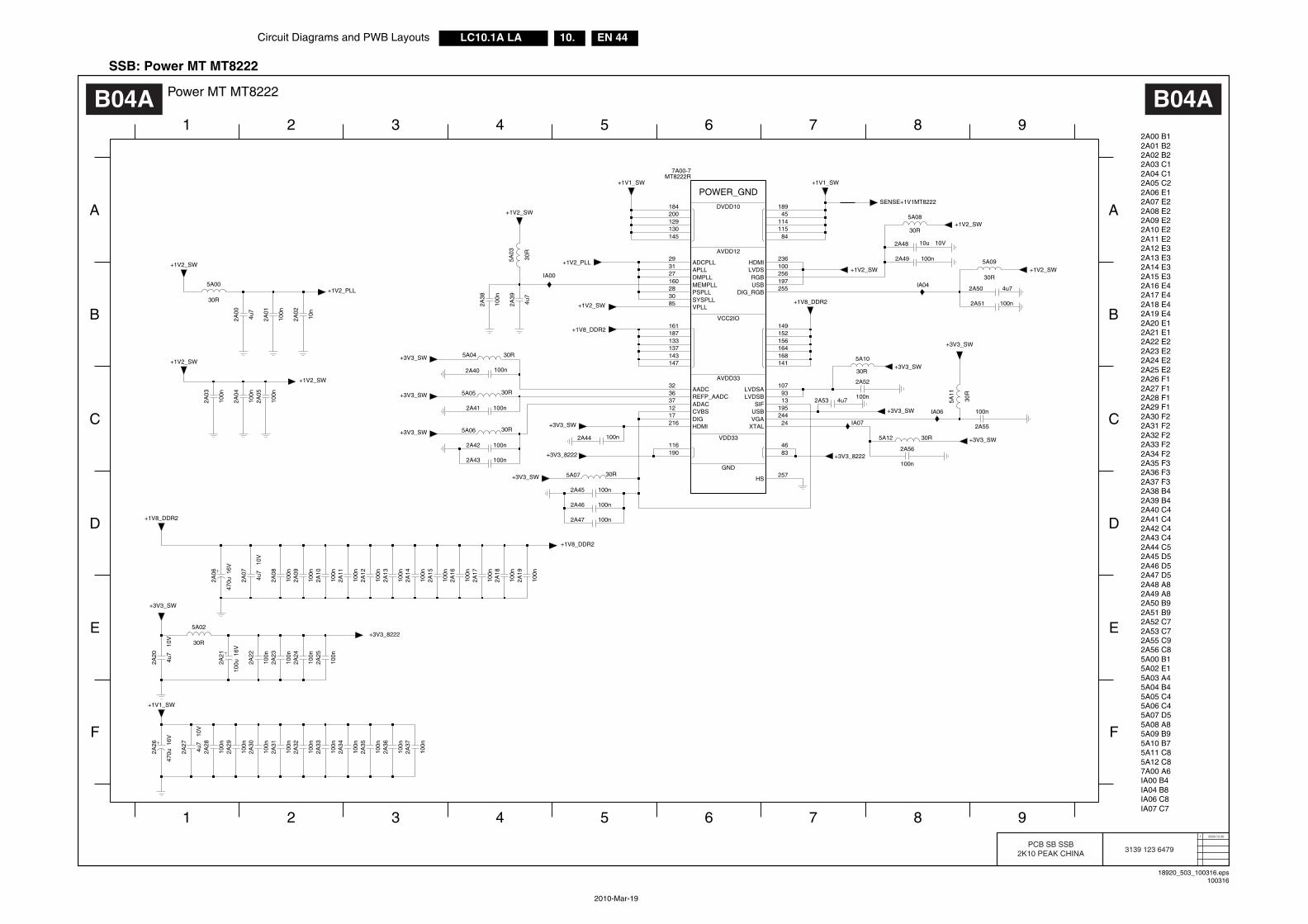
EN 44LC10.1A LA 10.Circuit Diagrams and PWB Layouts
2010-Mar-19
SSB: Power MT MT8222
18920_503_100316.eps100316
Power MT MT8222B04A B04A
2009-12-301
3139 123 6479PCB SB SSB
2K10 PEAK CHINA
DVDD10
AVDD12
VCC2IO
AVDD33
VDD33
GND
HDMIDIGCVBSADACREFP_AADCAADC
VPLLSYSPLLPSPLLMEMPLLDMPLLAPLLADCPLL
HS
HDMILVDSRGBUSB
DIG_RGB
LVDSALVDSB
XTALVGAUSBSIF
E
F
C
B
E
D
2A00 B12A01 B22A02 B2
2A07 E22A08 E22A09 E22A10 E2
2A15 E3
2
2A26 F12A27 F1
IA07 C7
53 4
IA06 C8
1 2 3 4 9
A
B
D2A43 C42A44 C5
A
F
2A03 C12A04 C12A05 C22A06 E1
2A16 E4
2A11 E22A12 E32A13 E32A14 E3
2A21 E12A22 E22A23 E2
1
2A25 E2
2A51 B92A52 C7
6 7 8 9
2A30 F22A31 F22A32 F22A33 F2
5 6 7 8
2A38 B42A39 B42A40 C4
C
2A42 C4
5A12 C87A00 A6
2A49 A82A50 B9
2A17 E42A18 E42A19 E42A20 E1
2A46 D52A47 D52A48 A8
2A24 E2
2A28 F12A29 F1
2A53 C72A55 C92A56 C8
2A34 F22A35 F32A36 F32A37 F3
10u
5A00 B15A02 E15A03 A45A04 B45A05 C45A06 C45A07 D55A08 A85A09 B95A10 B75A11 C8
2A41 C4
IA00 B4IA04 B8
2A45 D5
2A48 10V
100n2A47
5A11
2A15
100n
30R
156
116190
4683
161
164168141
187133137143147
149152
184
84
200129130145
18945
114115
257
1217216
107933613
19524424
27
236100
16028
256
30
197
85
32
37
7A00-7MT8222R
POWER_GND
2931
255
+1V2_PLL
+1V8_DDR2
2A56
100n
+3V3_SW
IA00
2A32
100n
100n
2A31
2A30
100n
100n
4u7
2A07
2A09
10V
30R
30R5A12
5A02
+1V8_DDR2
4u72A53
+3V3_8222
+1V1_SW
5A07 30R
30R
5A10
100n
2A13
10n
100n
2A02
4u7
2A01
30R
2A00
5A00
100n2A42
5A06
2A19
30R
100n
2A18
100n
2A17
100n
100n
2A16
2A14
+1V2_PLL
100n
+1V2_SW
+1V2_SW
2A40 100n
100n
2A23
470u2A
26 16V
100n2A51
+1V1_SW
2A50 4u7
SENSE+1V1MT8222
+3V3_8222
30R
5A08
2A44 100n
100n
2A05
30R
5A09
+3V3_SW
+3V3_SW
+1V2_SW
2A28
100n
IA07
IA06
100n
2A29
+3V3_SW
IA04
2A37
100n
2A36
100n
100n
2A35
2A34
100n
+1V2_SW
2A55
100n
+3V3_SW
100n
2A25
100n
2A24
2A22
100n
+3V3_SW
2A43 100n
2A04
100n
+1V1_SW
+1V8_DDR2
+1V2_SW30R5A04
100n
2A12
2A11
100n
100n
2A10
100n
2A08
+3V3_SW
470u2A
06 16V
2A33
100n
100n
2A38
2A46
+3V3_8222
+1V2_SW
+1V2_SW
100n
+3V3_SW
4u7
10V
2A20
2A03
100n +3V3_SW
+1V8_DDR2
2A41 100n
4u7
+1V2_SW
100n
2A39
+3V3_SW
2A49
30R5A05
5A03
30R
4u7
16V
100u2A
21
10V
2A27
100n
2A52
2A45 100n
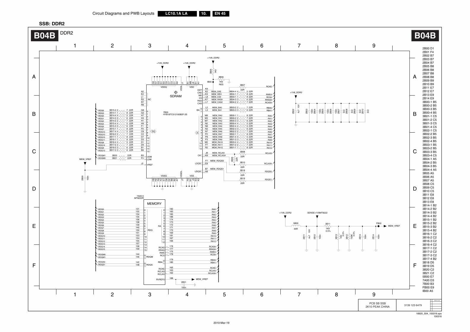
Circuit Diagrams and PWB Layouts EN 45LC10.1A LA 10.
2010-Mar-19
SSB: DDR2
18920_504_100316.eps100316
DDR2B04B B04B
2009-12-301
3139 123 6479PCB SB SSB
2K10 PEAK CHINA
1211109876543
0123456789
101112
CK
VD
DL
VREF
VS
SD
L
14
VDDQ
VSSVSSQ
BA
A
LDQS
UDQS
NC
DQ
CKEWE
ODT
RAS
1
CS
CAS
0012
VDD
LDMUDM
15
13
RDQ
RDQM
01
RDQS
RA
RBA
0123456789101112131415
01
23456789
101112
RCASRRASRWERCS
01
RCKERCLK0RCLK0
RVREF0
01
1
3B04-1 A5
3B15-1 B2
9
A
B
C
D
8
D
E
F
2B00 D12B01 F42B02 B7
2B07 B8
2B11 E7
2B06 B8
3B01-2 C53B01-3 C53B01-4 C53B02-1 C53B02-2 B5
1 2
3B04-2 B53B04-3 B53B04-4 A53B05 A53B06 A5
3 4 6 7 8 95
2 3 4 5 6 7
3B16-2 C2
E
F
A
B
C
2B08 B82B09 B92B10 B9
2B03 B72B04 B72B05 B8
3B01-1 C5
3B18 D5
3B02-3 B53B02-4 B53B03-1 B53B03-2 B53B03-3 B53B03-4 C5
3B21 C25B00 E77A00 D37B00 B3
IB00 A5
3B07 A53B08 C53B09 C53B10 C53B11 E83B12 E83B13 E83B14-1 B23B14-2 B23B14-3 B23B14-4 B2
3B16-3 C23B16-4 C23B17-1 C23B17-2 C23B17-3 C2
2B12 E72B13 E92B14 E93B00-1 B53B00-2 B53B00-3 B53B00-4 B5
3B15-2 B23B15-3 B23B15-4 B23B16-1 C2
3B19 D53B20 C2
FB00 E9
3B17-4 B2
10V
4u7
2B02
22R
3B19
F2
F8
H2
K3
N1
P9J7A7
H8
B2
B8
D2
D8
E7
C3
C7
C9
E9
G1
G3
G7
J2
A3
E3J3
A8
A1
E1
J9M9
R1
J1A9
G9
C1
A2E2L1R3R7R8
K9
K7
B3
B7
H1H9F1F9C8C2
F3F7E8
K8
L8
G8G2
D7D3D1D9B1B9
H7H3
N3N7P2P8P3
L2L3
L7
J8
K2
M8M3
M2P7R2
M7N2N8
ΦSDRAM
HYB18TC512160B2F-3S7B00
3B18
22R
4 5 22R3B14-4
2 7
FB00
3B14-2 22R
3B10
22R
22R
3B08
4 5
+1V8_DDR2
3B16-4 22R
2 7
3B21 22R
3B15-2 22R
175
22R3B20
138139140150151
144146
142148
177
188
132
153154155157158159
134135136
171170169
179180
176
165163162
178
281131183
181167166
185186174173172
MEMORY
MT8222R7A00-5
22R3B02-3 3 6
SENSE+1V8MT8222
3B17-1 1 8
3 6
+1V8_DDR2
22R
3B04-3 22R
1K0
3B05
1 8
2B05
100n
22R3B02-1
3B01-2 22R2 7
MEM_VREF
3B00-4 22R4 5
IB00
100n
2B03
22R3B16-3 3 6
3 6
3 6
3B14-3 22R
5
3B03-3 22R7
3B04-4 22R4
3B03-2 22R2
100n
8
2B04
3B15-1 22R1
22R3B15-4 4 5
1 8
22R
3B09
22R3B04-1
2B11
4u7
10V
2B12
100n
22R3B14-1 1 8 2B07
3n3
0.5%1K0
3B11
3B00-2 22R2 7
2B06
100n
2B09
3n3
3B01-3 22R3 6
+1V8_DDR2
3n3
2B10
3 6
MEM_VREF
22R3B15-3
2B14
100n
2B13
+1V8_DDR2
1 8
100n
5
3B03-1 22R
3B02-4 22R4
22R3B01-1 1 8
1K0
3B13
30R
5B00
0.5%
1 8
2 7
3B16-1 22R
22R3B16-2
3B07
22R
3 6
+1V8_DDR2
22R3B00-3
22R3B00-1 1 8
3B06
1K0RES
2B01
100n
3B17-3 22R3 6
4 53B17-4 22R
3n3
2B08
22R3B01-4 4 5
3B12
100K 0.
5%
4 57
22R3B03-422R3B17-2 2
2 7
MEM_VREF
3B02-2 22R
2 7
100n
2B00
22R3B04-2
RDQS0
RDQS1
RDQM1
RCKE
RCLK0#
RDQ3
MEM_BA1MEM_BA0 RBA0
RBA1
RCLK0
RCLK0#
MEM_RDQS1
MEM_RA6MEM_RA7MEM_RA8MEM_RA9MEM_RA10MEM_RA11MEM_RA12
RWE#RCS#
RRAS#RCAS#
RA7RA8RA9
RA10RA11RA12
MEM_RA1MEM_RA2MEM_RA3MEM_RA4MEM_RA5
RA6RA7RA8RA9
RA10RA11RA12
RCAS#RRAS#RWE#RCS#
RBA0RBA1
RCKERCLK0
RA4RA5RA6
MEM_WE#
RA0RA1RA2RA3
RA0RA1RA2RA3RA4RA5
RDQ13
RDQ0RDQ1RDQ2RDQ4RDQ5RDQ7RDQ12RDQ10
RDQM0MEM_RDQS0
MEM_RAS#MEM_CAS#
MEM_RCLK0
MEM_CKE
MEM_RCLK0#
MEM_CS#
RDQ6
RDQ15RDQ11RDQ8RDQ14RDQ9
RDQ0RDQ1
RDQ10RDQ11RDQ12RDQ13RDQ14RDQ15
RDQ2RDQ3RDQ4RDQ5RDQ6RDQ7RDQ8RDQ9
RDQM0RDQM1
RDQS0RDQS1
MEM_RA0
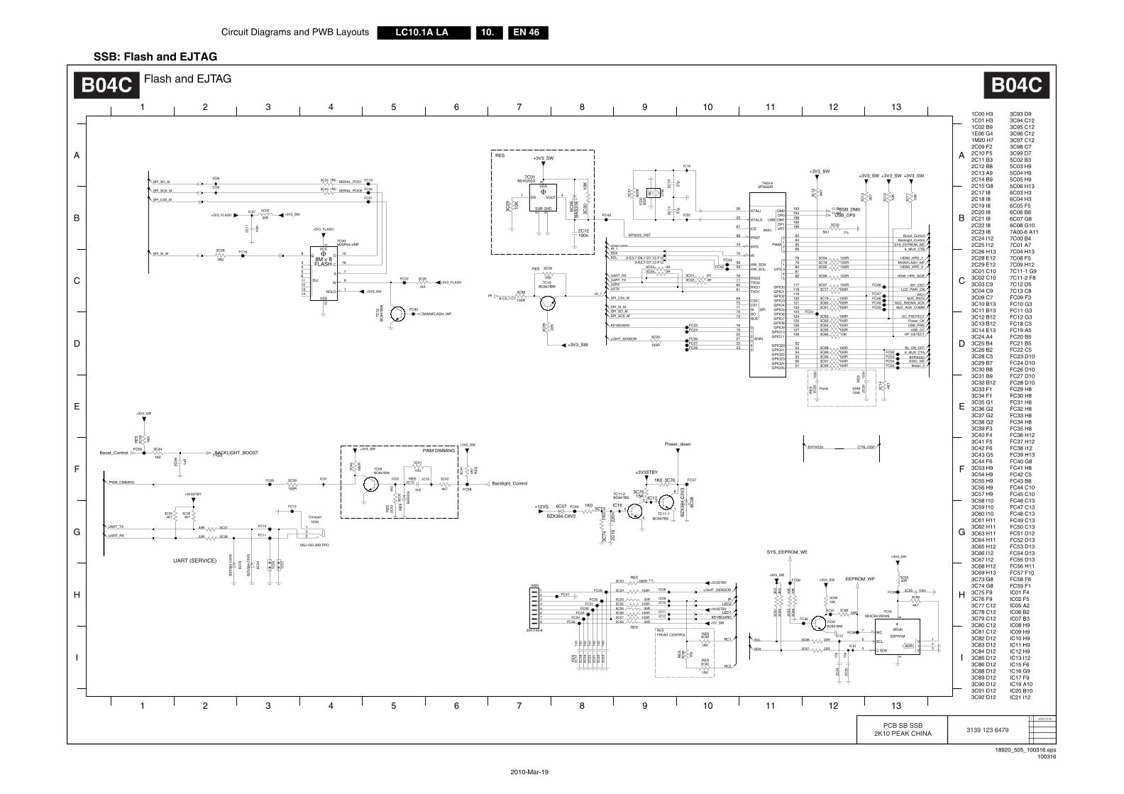
EN 46LC10.1A LA 10.Circuit Diagrams and PWB Layouts
2010-Mar-19
SSB: Flash and EJTAG
18920_505_100316.eps100316
Flash and EJTAGB04C B04C
2009-12-301
3139 123 6479PCB SB SSB
2K10 PEAK CHINA
NC
SCLADR
012SDA
WC
SUB
ER
GND
VOUT
VDD
DU
VCC
Q
VSS
D
C
S
W
HOLD
5
XTALI
XTALO
ICE
PRST
INT0
IR
HW_SDAHW_SCL
RXD0TXD0RXD1TXD1
CS0CS1SISOSCK
0
SPI
ADIN
USB
PWM
UP3
DM0DP0DM1DP1VRT
0123
01345
1234
0R
FRONT CONTROL
7 8 9 10 11
RES
4 5 6 7 8
B
C
D
E
F
G
H
I
1C00 H3
G
H
I
A
1C02 B91E06 G41M20 H72C09 F22C10 F52C11 B32C12 B82C13 A9
3 4 5 6 12 13
1 2
A
1206
Compair
2C24 I122C25 I122C26 H132C28 E122C29 E123C01 C103C02 C103C03 C93C04 C9
B
C
D
E
F
1C01 H3
3C32 B123C33 F13C34 F13C35 G13C36 G23C37 G23C38 G23C39 F33C40 F4
1 2
3
2C20 I82C21 I82C22 I82C23 I8
3C60 I103C61 H113C62 H113C63 H113C64 H113C65 H123C66 I123C67 I123C68 H12
9 10 11 12 13
3C14 E133C24 A43C25 B4
3C28 C53C29 B73C30 B83C31 B9
3C83 D123C84 D123C85 D123C86 D123C88 D123C89 D123C90 D123C91 D123C92 D12
2C14 B92C15 G82C17 I82C18 I82C19 I8
3C54 H9
3C56 H93C57 H93C58 I103C59 I10
6C03 H36C04 H36C05 F56C06 B86C07 G86C08 G107A00-6 A117C00 B47C01 A7
3C09 C73C10 B133C11 B133C12 B123C13 B12
3C77 C12
3C26 B2
3C79 C123C80 C123C81 C123C82 D12
FC09 F3FC10 G3FC11 G3FC12 G3FC18 C3FC19 A5FC20 B5FC21 B5FC22 C5
3C41 F53C42 F63C43 G53C44 F63C53 H9
3C98 C73C99 D7
3C55 H9
5C03 H95C04 H95C05 H95C06 H13
FC33 H8FC34 H8FC35 H8FC36 H12FC37 H12FC38 I12FC39 H13FC40 G8FC41 H8
3C69 H133C73 G83C74 G83C75 F93C76 F9
3C78 C12
7C12 D57C13 C8
PWM DIMMING
FC47 C13FC48 C13FC49 C13FC50 C13
3C93 D93C94 C123C95 C123C96 C123C97 C12
SDM
UART (SERVICE)
5C02 B3
FC29 H8FC30 H8FC31 H8FC32 H8
FC57 F10FC58 F6FC59 F1IC01 F4IC02 F5IC05 A2IC06 B2IC07 B3IC08 H9
7C04 H137C08 F57C09 H127C11-1 G97C11-2 F8
IC17 F9IC19 A10IC20 B10IC21 I12
0R
FC23 D10FC24 D10FC26 D10FC27 D10FC28 D10
0R
0R
Panel
RES
FC56 H11
FC42 C5FC43 B8FC44 C10FC45 C10FC46 C13
IC11 H9IC12 H9IC13 I12IC15 F6IC16 G9
FC51 D12FC52 D13FC53 D13FC54 D13FC55 D13
IC09 H9IC10 H9
IC09
FC29
IC07
FC22
2C13
27p
27M
3225
1C02
3C85 100R
22R3C66
3C89 100R
6C08
3C39
100R
BZ
X38
4-C
3V3
+3V3_SW
FC32
IC15
3C57 100R
3K3
3C61
3C90
+3V3_SW
+3V3_SW
100R
+3V3STBY
BC847BW7C08
FC31
FC46
FC47
FC51
FC18
FC38
3C354K7
FC39
100R3C56
RE
S
+3V3_SW
3C58
1R0
4K7
+3V3_SW
1u0
3C36
2C09
680R
3C40
3C53 1%680RRES
FC35
100R3C77
5K1
3C32
1%
FC24
123
6
5
84
7
M24C64-WDW6
(8Kx8)
Φ
EEPROM
7C04
3C33
1K0
RE
S
FC23
3C82
2C23
1n0
100R
4K7
3C69
1K0 3C76
6C03
BZ
X38
4-C
6V8
3C86 10K
1K0
RE
S3C
43
3C98
100R
15K3C75
1R0
3C26
2C20
IC06
1n0
100R3C843C83 100R
FC34
5C04 30R
3C62
3K3
3C96 100R9
1K0
3C74
11121314
1
8
7
210
16
15
3456
Φ8M × 8FLASH
M25P64-VMF7C00
BZ
X38
4-C
6V8
6C04
Φ1
325
4
BD45292G7C01
3C12
4K7
2C26 100n
+3V3_SW
5C03 30R
3C14
4K7
+3V3_SW
3C31
FC49
IC05
820K
100R
+3V3_FLASH
3C81
+3V3_FLASH
2C19
1n0
3C023C01
1n0
2C22
+3V3_SW
IC13
33R
FC48
FC19
3C37
Power_down
FC33
+3V3STBY
5
3
4
+12VS
+3V3_FLASH
BC847BS7C11-2
FC37
FC36
3C34
1K0
IC10
3C92 100R
4K7
3C13
FC30
+3V3_SW
7C11-1
2
6
1
10K
BC847BS
+3V3_SW
3C29
100n
2C11
RE
S
13
3C44
4K7
1E06
MSJ-035-29D PPO
2
FC55
FC21
FC20
1C01
IC16
IC17
1K0
3C28
FC12
3C6833R
FC10
3C91
+3V3STBY
22K
100R
FC45
3C99
3C95
IC01
100R
FC53
FC50
FC52
2C14
+3V3_SW
27p
220n
2C15FC11
3C09
1R0
100R3C78
RES
3C11
10K
3C97 100R
100n
2C28
RE
S
1n0
2C18
7C12
BC
847B
W
FC09
BA
S31
66C
06
1R0
3C60RES
RE
S
BA
S31
6
6C05
100R3C80
+5V_SW
3C24 1R0
+3V3_SW
FC57
3C94 100R
10K
3C10
+3V3_SW
FC58
FC59
BZX384-C8V2
30R5C06
6C07
10K
3C30
FC27
BC847BW7C13
FC56
3C55 100R
RES
1C00
30R5C05
2C12100n
1R0
RES
FC26
3C59
100R3C79
2C10RES
2u2
RE
S 100n
2C29
10K
3C38
3C63
33R
2C25
10p
3C67 22R
2C21
1n0
FC44
FC54
IC20
FC42
3C42
4K7
1-G3
6-C5,7-C7
+3V3_SW
10p
2C24
7C09BC847BW
IC21
IC19
2-E2,7-D7,12-F12
FC28
11-B411-B4
2-E3,7-D6,7-D7,12-F12
1R0
3C41
FC41
3C25 1R0
RE
S
+3V3STBY
2C17
1n0
10K3C65
FC43
IC11
10K
3C64
IC12
3C93
100R
IC08
IC02
3C88
FC40
100R
196
26
25
5C02
30R
77
61
7879808182
193
198194
199
646566
76
60
6973
72
7170
124
GPIO8125
GPIO9126
5958
67
74
75
3686
54
GPIO2355
GPIO245657
GPIO25
GPIO3120
GPIO4121
GPIO5122
GPIO6123
GPIO7
GPIO0117
GPIO1118
127GPIO10GPIO11
128
GPIO2119
GPIO2052
GPIO2153
GPIO22
MT8222R
MISC
181920212223
7A00-6
100R3C54
8
1K03C73
2041145-8
1234567
1M20
3C043C03
MAINFLASH_WP
MAINFLASH_WP
MT8222_RST
IR_1
EEPROM_WP
UART_TX
U2TXU2RX
UART_RX
SYS_EEPROM_WE
PSID-LRTCnSSAPYB
SERIAL_PDD1
IR
DC_PROTECT
WCn
HP_DETECT
BL_ON_OFF
IR_1
PWM_DIMMING
HDMI_HPD_1
HDMI_HPD_2
HDMI_HPD_SIDE
INT_CEC
SERIAL_POOE
SPI_CS0_M
MJC_RXDMA_ACKMJC_RST#
LCD_PWR_ON
SYS_EEPROM_WEBacklight_Control
Boost_Control
SPI_SCK_MSPI_SO_MSPI_SI_M
SPI_CS0_M
SCLSDA
KEYBOARD
Muten_2
BYPASSn
A_MUX_CTBPOWER_DOWN
EDID_WE
A_MUX_CTA
USB_OCUSB_PWEPower_OK
MJC_ACK_COMM
USB_DP0USB_DM0
LIGHT_SENSOR
KEYBOARD
LED2
LED1
SPI_SI_M
BACKLIGHT_BOOST
SPI_SO_M
UART_TX
IR
UART_RX
RC1
RC2
SPI_SCK_M
SDA
SCL
LIGHT_SENSOR
Boost_Control
Backlight_Control
Circuit Diagrams and PWB Layouts EN 47LC10.1A LA 10.
2010-Mar-19
SSB: Stand-by
18920_506_100316.eps100316
Stand-byB05 B05
2009-12-301
3139 123 6479PCB SB SSB
2K10 PEAK CHINA
NC
SUB
ER
GND
VOUT
VDD
6
67
GPIOD
01234567
GPIOE
VDD
01234567
I
O
CL
DA
NRST
012345
VSS
OSC
DS1
GPIOA
012345
GPIOB
NC
GPIOC
012345
5D01 A26D00 A3
6D03 E56D04 E6
ID02 A5ID03 B4
FD03 D3FD04 D3
3D16 A23D17 B6
FD05 E3FD06 E3
3D20 C63D23 C6
FD07 E3FD08 E3FD09 C6FD10 B3FD11 C4FD12 D4FD13 D3FD14 D4FD15 D4
NC
4D04 C34D05 D65D00 A2
2D04 A42D05 C2
6D01 D36D02 D2
2D08 D32D27 B6
7D00 B57D01 D67D02 A37D03 B37D05 C27D06 C2FD00 A2FD01 B6FD02 B6
FD16 D6ID00 C6
3D09 D23D11 D23D12 D23D13 D23D14 E23D15 E2
3D18 B63D19 C6
1 2
3D24 C33D25 D73D26 D73D27 D63D28 D13D71 D3
4D01 D34D02 C34D03 C3
RESERVED
2D01 A22D02 B42D03 B4
TO ANALOG/IOs
2D06 D22D07 D2
3D00 B23D01 B23D02 A43D03 B43D04 B43D05 C33D06 C33D07 C33D08 C3
ISP PROGRAMMING
1D04 E32D00 A2
NC
3 4 5 6 7
1 2 3 4 5 6 7
A
B
C
D
E
A
B
C
D
E
1D03 B5
3D14 100R
7D01BC847BW
+3V3STBY
+3V3STBY
FD13
FD03
2-E3,6-F5,7-D6,12-F12
4D05RES
6.3V
22u
2D01
RES
+3V3STBY
25
4
3D12 10K
BD45275G7D02
1
3
FD00
Φ
FD01
4D01
6D00
BA
S31
6
234
56
1D04502382-0470
1
22p2D04
12M
+3V3STBY
1D03
2D08 100p
FD04
RES
4K7 RES
+3V3STBY
3D18
7D06BC847BW
1
3
2
6D03
BAS316
RES
FD05
FD12
ID02
FD10
FD11
FD16
RES
4D02
4K73D17
3D13 RES
100R
10K
2D07
3D196-D5
10n
100n
2D27
100R3D15
10K
3D00
4D03 RES
10n
2D00
BAS316
6D04
+3V3STBY3D04 22R
ID03
3D16
2D02
100n
10K
1
3
2R
ES
RESBC847BW7D05
3D0810K
10K3D71
RES
RES
10K
+3V3_SW
3D07
3D02
10K
FD09
22p
9-B
8
6-G6
8-C
4,8-
D6
2D03
2-E3,6-F5,7-D7,12-F12
9-C7
6-E3
RES 6D01 BZX384-C6V8
ID00
+3V3STBY3D23100R
3D26
+3V3STBY
10K
22K
3D25
10K
3D01
6-F3
100n
FD02
6-B5
2D06
10K
FD07
3D05
3D03
FD06
22R
3D11 22R
3D27
10K
2D05100n
1132448
46
5
4
2
3
3231
4745444342414039
17161514
383736353433
1211109876
2120191823
22
302928272625
7D00WT61P7-RG480
Φ
RES
3D2410K
FD08
3D28
4K7
10K
6-C5
6-C5
RES3D06
NC1
2 SCL0 SCL1 7
SDA03 SDA1 6
VCC
8 7D03PCA9515A
EN5GND
4
3D20
4K7
5D00 30R
+3V3_SW
4D04 RES
BAT54 COL
6D02 27K
FD14
3D09
FD15
30R
5D01
IR
MUTEN_1
RESET_AUDIO
MUTEN
MUTEN_2
CEC_HDMI_SOC
RXD_WTTXD_WT
STBY_SCLSTBY_SDA
MT8222_RST
STANDBY
STBY_SDA
INT_CEC
STBY_SCL
SCL
KEYBOARD
SDA
LED1
LED2
POWER_DOWN
EN 48LC10.1A LA 10.Circuit Diagrams and PWB Layouts
2010-Mar-19
SSB: I/Os HDMI
18920_507_100316.eps100319
I/Os HDMIB06A B06A
2009-12-301
3139 123 6479PCB SB SSB
2K10 PEAK CHINA
3E46 G124E00 I12
FE09 F5FE10 F5FE11 F5FE12 F5FE13 F7
7E07 H6
4E03 B25E03 B26E00 B86E01 F8
FE14 G7FE15 H8
7E00 C87E01 F8
FE16 I5
1P05 H5
FE17 I5
7E05 D7
3E07 D6
2E03 B3
IE01 I11IE02 I12
2E04 B3
3E04 C73E05 C7
FE08 E5
FE23 K8FE24 C13FE25 I11
3E42 J12
IE00 H12
3E20 G7
4E01 F124E02 G11
1P03 A5
2E01 F82E02 I8
2E00 C8
3E02 C7
3E37 D13
3E06 C7
FE04 B5
FE20 I5FE21 I7FE22 J7
3E10 D63E11 D8
3E16 G63E17 G5
FE26 I12
3E21 G6
3E40 D13
3E18 G7
3E41 I11
1P02 E5
3E29 J63E30 J7
3E33 J83E34 K6
3E01 C7
FE18 I5
3E38 D13
7E12 I127E13 G127E14 H127E15 F12FE00 A5FE01 B5FE02 B5FE03 B5
FE05 C7FE06 C7
3E25 J73E26 J7
3E35 C133E36 C13
FE07 D8
3E39 D13
3E08 D53E09 D6
6E02 I87A00 B11
3E14 G73E15 G7
7E02 J87E04 D6
3E19 G7
7E08 G7
FE19 I5
7E11 K87E10 K6
3E22 G63E23 G8
3E27 J63E28 K5
3E31 J73E32 J7
RX0
00B11B22BCCB
RX1
00B11B22BCCB
RX2
HDMI
2BCCB
PWR5V_1
PWR5V_2
CEC
SCL0SDA0
SCL1SDA1
SCL2SDA2
PWR5V_0
00B11B2
SCLADR
012SDA
WC
SCLADR
012SDA
WC
SCLADR
012SDA
WC
1
A
B
C
D
E
5
I
6
NC
2 3 4 14 15
1 2 8
NC
F
G
H
TO
FLA
SH
&N
VM
A
B
E
F
J
L
TO FLASH&NVM
5 6 7 13 16 17
4 7
NC
9 10 11
I
J
K
L
17
C
D
H
K
NC
8 9 10 11 12
HDMI 1
3
HDMI 2
15 1612 13 14
G
+3V3STBY
HDMI SIDE
7E14BSH111
RES
FE08
+5V_HDMI_2
FE09
FE25 FE26
FE24
212223
19
23456789
20
1
101112131415161718
1P0310029449-001RLF
FE13
100R3E02
8-F7
FE06
8-B7
47K3E23
3E35 100R
4
7
7E00
123
6
5
8
M24C02-WMN6
EEPROM
Φ(256 × 8)
22K3E09
3E06
10K
3E04
47K
3E25
3E26100R
211206205
100R
222221224223218217
208207210209212
231230233232235234229228
220219
201
227
215
204
226
214
203
225
213
202
HDMI
MT8222R7A00-3
1K0
3E10
6-F3
100R3E36
100R3E37
BC847BW7E11
3E40 100R
2E02 100n
3E31
47K
3E05
47K
7E04BC847BW
4
7 (256 × 8)Φ
EEPROM
M24C02-WMN6
123
6
5
8
7E01
100R
3E41
FE14
2
3
+5V_HDMI_26E00BAT54C
1
FE05
FE21
8-B7
8-C9
1K03E16
6-E3,8-D7,8-F7,11-D2
RES
3E46
22K
+3V3_SW
8-E9
8-G9
FE11
6-F3FE23
3E2922K
FE12
FE19
FE04
FE00
+5VHDMI_2
BC847BW7E07
BC847BW7E10
3E22
1K0
47K
3E30
7E13BC847BW
RES
FE10
20212223
171819
23456789
1
10111213141516
+5V_HDMI_2
10029449-001RLF1P05
2E00 100n
BC847BW7E05
+5V_HDMI_A
3E38 100R
100R3E39
4E01
21
3
4E02
8-D7
BAT54C6E01
3E18
47K
+5V_HDMI_1
+5V_HDMI_SIDE
1K03E27
3E2122K
100K
89
20212223
3E17
1516171819
234567
1
1011121314
1P0210029449-001RLF
3E32
10K
FE20
FE07
FE17
FE18
FE16
+5VHDMI_1
22K
3E42
6-F3
RES
3E28100K
FE22
10K
3E20
47K3E33
IE00
+5VHDMI_SIDE
+5V_HDMI_1
100n2E01
47K3E11
3E34
1K0
FE01
+5V_HDMI_SIDE
IE01
+3V3_SW
3E071K0
8-C9
+5V_HDMI_1
47K
3E19
2E04
RE
S
100n
RE
S
10u
2E03
RES
30R
5E03+5V_HDMI
+3V3STBY
RES
BC847BW7E12
+5V_HDMI_A
IE02
8-H98-H9
8-H98-H9
8-H9
8-G9
BC847BW
8-G9
7E08
6E02BAT54C
21
3
FE15
FE03
FE02
+5V_HDMI_SIDE
4E00
+5V_HDMI_A
3E08100K
6-E3,8-B7,8-D7,11-D2
100R3E01
3
1
2
RESBSH111
7E15
100R3E15
3E14
5
84
7
100R
7E02
123
6
+5V_HDMI_A
M24C02-WMN6
EEPROM
Φ(256 × 8)
4E03
7-C5,8-D6
7-C5,8-C4 8-G4
8-D4
8-C9,8-E9,8-G9
HDMI_HPD_1
8-H9
CEC_HDMI_8222CEC_HDMI_SOC
CEC_HDMI_SOC
RX1_0p
RX2_CnRX2_CpRX2_2nRX2_2pRX2_1nRX2_1pRX2_0nRX2_0p
RXSide_1nRXSide_1pRXSide_0nRXSide_0p
RX1_CnRX1_CpRX1_2nRX1_2pRX1_1nRX1_1pRX1_0n
HDMI_HPD_2
DDC_SCL_HDMI_1DDC_SDA_HDMI_1
DDC_SDA_SIDE
DDC_SDA_SIDE
CEC_HDMI_8222
RXSide_CnRXSide_CpRXSide_2nRXSide_2p
CEC
DDC_SCL_HDMI_2DDC_SDA_HDMI_2
DDC_SCL_SIDE
DDC_SCL_SIDE
EDID_WE
DDC_SDA_HDMI_2DDC_SCL_HDMI_2
DDC_SCL_HDMI_1DDC_SDA_HDMI_1
DDC_SCL_SIDEDDC_SDA_SIDE
EDID_WE
HDMI_HPD_SIDE
EDID_WE
RX2_1nRX2_0p
RX2_0nRX2_Cp
RX2_Cn
RXSide_2n
RXSide_2p
CEC
CEC
CEC
RX2_2p
RX2_2nRX2_1p
RXSide_Cn
RXSide_CpRXSide_0n
RXSide_0pRXSide_1n
RXSide_1p
RX1_2p
RX1_2nRX1_1p
RX1_1nRX1_0p
RX1_0nRX1_Cp
RX1_Cn
B04C
B04
C
Circuit Diagrams and PWB Layouts EN 49LC10.1A LA 10.
2010-Mar-19
SSB: I/Os Audio
18920_508_100316.eps100319
I/Os AudioB06B B06B
2009-12-301
3139 123 6479PCB SB SSB
2K10 PEAK CHINA
3F50 B83F52 A9
3F14 D63F15 D63F16 D63F17 D33F18 D3
IF07 B5IF08 B8
7F04-1 B87F05 B8FF00 B7FF02 D2
3F27 F43F28 F53F29 F53F30 F53F31 D73F32 D73F33 E9
2F36 H52F37 H6
2F50 E11
FF15 D7FF16 D7FF17 D9FF18 D9IF00 B2IF01 B2
3F53 A83F60 G33F61 G33F62 G33F63 G53F68 E93F69 E9
3F12 D63F13 D6
2F15 D82F16 D8
2F19 C11
1F04 F2
4F01 A10
IF10 D3IF11 D3IF13 E3IF14 E3
FF03 E2FF04 F2FF05 F3FF06 G2FF07 G2FF08 G2FF09 H2
3F25 E3
3F26 E9
2F34 H42F35 H5
2F48 D62F49 E11
FF10 H2
IF02 B4IF03 B4IF04 B4IF05 B4IF06 B5
3F46 B83F47 F3
3F10 D53F11 D5
2F13 E32F14 E3
2F17 E82F18 E8
1E07 F21E09 D1
6F00 D26F01 E26F02 A86F03 H36F04 H46F05 H4
IF15 A8IF16 E6IF17 F6
7F02 F67F03 F5
3F23 E53F24 E3
2F32 F32F33 H3
2F04 B4
3F34 E93F35 B73F37 B9
FF11 D11FF12 D11FF14 F5
3F44 F53F45 F5
3F08 C53F09 D5
2F11 D32F12 E2
1F17 H22F00 B2
1328 G2
1F02 D21F03 E2
2F21 C112F22 C9
2F25 D112F26 E102F27 E11 7A00-2 C10
7F00 B47F01 D8
3F21 E53F22 E5
2F30 E122F31 F3
2F03 A4
3F00-1 B33F00-2 A43F00-3 B33F00-4 A43F02 B33F05 B5
2F07 B52F08 B8
3F41 F33F42 F63F43 F6
3F06 B53F07 B5
2F09 D22F10 D3
2F01 B22F02 A4
2F05 C32F06 B5
2F23 C92F24 D11
2F20 C11
3F19 E93F20 E5
2F28 E112F29 E11
VIAGND_HS
VOIN-
VDD
1
SHUTDOWN
BYPASS
2
GND
2
1
G4
0
32
VDD
VEE VSS
10
321
4X03
01
AVICM
AL1AR1
AL2AR2
AL3AR3
SPDIF_OUT
SIFPSIFN
AF
VMID
AIN_LAIN_R
AOMCLKAOLRCKAOBCLKAOSDATA0ADIN
RES
RES
9
RIGHT
1 2 5 6
SPDIF
E
10
F
G
From GP10
11 12
3 4
B
7 8 11
HEADPHONE
RES
D
E
H
9 101 2
C
D
5 6
B
C
F
G
H
A
RE
S
7 83 4
12
A
LEFT
1n0
2F37
33R3F08
IF03
RE
S
1n0
2F10
FF10
FF14
IF01
3F45
10K
100n
2F22
22K
FF02
3F20
4u7
2F21
2F01 1u0
+3V3_SW
3F06 33R
22K
3F14
3F24
1R0
+Va_MUX
3F27
22K
2F18
10u
3F15
1n0
2F09
22K
RE
S
7-C7
3F16
22K
9-G3
RE
S2F
291n
0
IF10 IF11
3F611R0RES
RE
S2F
12
1n0
3F10
22K
4F01
22K
3F46
3F47
3F18
RE
S10
0R
47K
FF16
AUD_GND
FF15
+3V3STBY
3F44
10KBC847BW7F03
10K
3F43
10K
3F42
BC847BW
+Va_MUX
7F02
2F07
220u 6.3V
3F33
22K
2F17
10u
3F21
22K
3F22
22K 3F32
RES
100R
3F26
1K0
100R3F31
3F60 1R0
+3V3_SW
22K
3F53
3F00-4 22K4 5
33p
2F03
2F14
2F27
RE
S
10u
1n0
FF17
FF18
IF14IF13
FF12
IF15
FF11
FF03
IF00
RE
S3F
50
22K
33R
RE
S
3F05
2F36
1n0
1F04
22K
3F12
6.3V
1
7
220u
2F06
4 9
2
6
5
8
1011
7F00TPA6111A2DGN
AMPLIFIERΦ
3
1F17
10n2F50
10u
2F16
FF08
3F09
22K
2F15
100n
2F08
1u0
100n
2F32
2F02
33p
2F11
10u
2F49 10n
2F23
3F00-2 22K2 7
10u
PE
SD
5V0S
1BA
FF06
RE
S6F
00
6
+3V3_SW
3F00-3 22K3
2F30
1n0
RE
S
2F19 4u7
3F23
22K
3F37
10K
3F69 RES
1K0
1F03
13
3
IF16
7 8
12
1
14
5
15
2
11
4
7F01HEF4052B
MDX
109
6
16
1K0
3F19
10K
3F52
RE
S
+3V3_SW
2F34
1n0
IF05
AUD_GND
BC847BPN(COL)7F04-1
2F31
33p
FF07
+Va_MUX
IF06
3-B73-B73-C73-C73-C7
3-C73-C7
IF07
1R03F62
3
45
78
1E09MSJ-035-10A B AG PPO
1
2
2F00
1u0
1u0
2F05
3F17
1R0
FF05
3F68
1K0
10u
22K
3F28
2F48
3F29
22K
3F30
22K
IF08
1
2
3
45
78
1328
MSJ-035-10A B AG PPO
22K
3F35
22K
3F11
6F04
1n0
2F33
RE
S
2F28
1n0
RE
S
FF00
100R
3F41
3F02
10K
8
3-C7
AUD_GND
3F00-1 22K1
3F13
22K
FF04
4847
50
44
41
39
42
1514
62
33
MT8222R7A00-2
AUDIO
51
16
3435
43
40
3849
+3V3STBY
100n
2F20
FF09
2F35
RE
S
1n0
3F63
1R0
1
3-D7
1E07
YKB11-0946V
CON_JACK
2
33R3F07
100n
2F26
PE
SD
5V0S
1BA
6F03
2F25 10u
6F05
PE
SD
5V0S
1BA
6F02
IF17
BAS316
1F02
+Va_MUX
BC847BW
3F34
22K
7F05
RE
S3F
25
47K
1u0
2F04
IF02
IF04
2F13
RE
S
1n06F
01
PE
SD
5V0S
1BA
RE
S
10u2F24
AIN0_L
A_MUX_CTB
MUX_CTB
AIN3_R_PCAIN2_RAIN1_RAIN0_R
AIN2_LAIN3_L_PC
AIN1_LHP_LHP_R
AUD_L
AUD_R
A_MUX_CTA
MUX_CTA
SPDIF_OUT_RCA
SPDIF_OUT_RCA
RC2
RESET_AUDIO
RC1
HP_LOUT
HP_ROUT
HP_DETECT
RESET_AUDIO
HP_R
HP_L
MUTE
MUTEN
HP_ROUT
HP_LOUT
SIF_OUTSIF_OUT_GND
AUDIO_LAUDIO_R
A_STBY
AIN3_R_PC
AIN3_L_PC
AOBCKAOLRCKAOMCLK
AOSData0
EN 50LC10.1A LA 10.Circuit Diagrams and PWB Layouts
2010-Mar-19
SSB: I/Os YPbPr
18920_509_100316.eps100319
I/Os YPbPrB06C B06C
2009-12-301
3139 123 6479PCB SB SSB
2K10 PEAK CHINA
6G13 D8
5G01 D45G02 D4
1G04 B10
3G32 D9
6G05 B10
2G02 B5
FG02 C5
2G04 B4
FG04 D5
IG01 B4
6G00 C46G01 C46G02 B46G03 A106G04 B10
6G06 C10
1G05 B101G06 C10
5G05 C9
3G56 D8
FG10 C11FG11 C11
2G44 D42G50 G22G51 G22G52 D9
5G03 B105G04 C10
3G53 G2
3G57 E8
IG25 F10
3G63 E105G00 C4
1G02 D51G03 A10
FG25 G4
1E01 C6
2G39 F92G40 F10
FG03 D5
6G12 G8
IG26 G10
FG06 B11FG07 B11
2G00 A32G01 B4
2G03 B3
2G05 B5
FG05 A7
3G14 D33G15 E3
2G09 D2
3G39 F83G41 E103G42 F93G44 G9
FG08 B11FG09 C11
6G14 E86G15 B4
3G09 C3
3G11 C4
2G35 F9
1G00 C51G01 D5
FG23 D9FG24 E9
IG00 A4
2G41 G82G42 G9
6G16 D47A00 E3FG00 C6FG01 C5
6G07 D106G10 F86G11 F8
1G13 D81G14 E8
IG08 B9
IG13 D4
2G06 C2
2G10 D22G11 D2
2G15 A82G16 A92G17 A102G18 A8
3G29 C83G30 D8
3G04 A43G07 B4
2G23 C9
3G10 C4
2G25 C7
1E02 B121E08-1 G71E08-2 F71E08-3 F71E10 E6
FG21 C5FG22 A7
FG16 G72G43 G10
1G11 F81G12 G8
IG06 A9IG07 A9
IG09 B7
IG23 F9
3G61 D10
2G37 E102G38 F8
3G12 D3
2G26 C7
2G12 E2
2G55 E103G00 G4
2G21 B72G22 B9
2G24 C7
3G23 A10
3G13 D3
2G07 C4
FG17 G8FG20 E7
IG24 G9
IG03 D3IG04 E3
FG14 E7FG15 F8
2G27 D72G28 D9
1G07 C101G10 F8
2G53 E92G54 D10
2G19 B92G20 B10
2G08 C4
3G17 D43G20 A10
3G24 B8
3G25 B93G26 C93G27 C83G28 C8
IG02 C3
CVBS
CVBS
CVBS
VGA
COM1SY0SC1SY1
VSYNCHSYNC
SDASCL
BYPASS0BYPASS1
COMCOM0
SOG
RPGPBP
Y0PPB0PPR0PSOY0
Y1PPB1PPR1PSOY1
0P0N1P2P3P
SC0
CVI-2
F
H
Y
C
(YELLOW)
1 2
CVI-1
(RED)
D
E
G
A
C
D
5
AVin
AVin
SVHS
7 8
LEFT
6
CVBS
B
C
6
RIGHT
B
3 4 7
12
A
10 11 12
3 4
E
F
G
1 2
H
(WHITE)
9 10 11
8 95
3G13
1R0
3G32
75R
2G50
IG23
47n
2G26 10n
FG14
FG17
1G07
RE
S6G
05
1G03
CD
S4C
12G
TA
5G00
0001
60R
RE
S2G
38
1n0
RE
S
10u
2G15
2G19
1n0
RE
S
1n0
2G16
1R03G28
3G23
1R0
68R
3G12
RE
S6G
02
CD
S4C
12G
TA
1R0
2G54
3G15
1n0
47n
RE
S2G
04
1R0
IG00
3G44
IG04
2G00
10u
IG07
2G39
1n0
1G04
RE
S
1G11
1G12
10n2G246G00
RE
S
CD
S4C
12G
TA
3G10
75R
1112
23
4
5
6
7
8
9
MSP-636H1-011
10
1E02
68R3G29
10u
2G03
5G05
68R
3G14
60R
10n
2G091R0
FG20
IG25
3G30
2G07
15p
3G57
75R
1G14
RE
S
1n0
2G02
2G21
10n
3G04
1R0
3
4
1E08-2WHITE
MSP-305H-BBB-432-03 NI
FG01
2G53
47p
237
251
246
238
253
248
254
249
243
240
250
245
192191
765
1011
3
14
2
241
MT8222R
7A00-1
ΑΝΑΛΟΓ
239
242252247
98
FG04
3G63
100R
100R
3G61
FG00
1R0
FG23
3G20
2G22
15p
FG24
1G0115
p
2G08
60R
3G53 100R
5G02
75R
3G39
47n
2G55
FG02
2G18
10u
15p
2G44
RES
CD
S4C
12G
TA
6G13
15p
2G28
47p
IG09
2G35
47p
2G52
5G01
60R
RE
S
1n0
2G05
IG01
RE
S
1n0
2G42
3G09
68R
1G02
FG06
IG03
2G43
10u
68R
3G24
1n0
2G17
RE
S
1G06
1G00
IG06
1u02G51
FG09
FG22
RE
S
1n0
2G41
1n0
2G01
RE
S
FG07
FG08
10n2G27
FG11
2G12
10n
IG08
FG16
1G10
75R
3G17
RE
S
1R0
CD
S4C
12G
TA
6G01
RE
S3G
00
IG24
6G10
CD
S4C
12G
TA
RE
S
FG05
6G14
CD
S4C
12G
TA
RES
3G11
75R
RE
S
CD
S4C
12G
TA
6G11
IG26
60R
5G04
101112
23
4
5
6
7
8
9
1E011 MSP-636V1-01
47n
2G37
IG02
2G20
1n0
RE
S
4n7
2G10
FG10
2G11
RE
S
CD
S4C
12G
TA
10n
3G25
75R
6G06
FG21
1R0
3G07
4
756
1
2
31E10
MDC-066H-A LF
FG15
10u
2G40
3G26
5G03
75R
60R
IG13
1E08-1RED
MSP-305H-BBB-432-03 NI
5
6
6G12
CD
S4C
12G
TA
RE
S
2G06
10n
3G41
100R
10-F1
3G42
FG25
1R0
FG03
1
2
3G56
75R
1E08-3YELLOW
MSP-305H-BBB-432-03 NI
1G13
CD
S4C
12G
TA
6G07
RE
S
1G05
3G27 68R
6G16
CD
S4C
12G
TA
RE
S
15p
2G23
6G03
RE
S
CD
S4C
12G
TA
CD
S4C
12G
TA
6G15
6G04
CD
S4C
12G
TA
RE
S
RE
S
47n2G25
11-F2
Y1P
AINI_L_AV2
AINI_R_AV2
AINO_R_AV1
AINO_L_AV1
PB0P
PR0PSOY0
Y0P
PB1PPR1PSOY1
RP
SOG
VSYNC
CVBS_RFGND_CVBS_RF
SY0
SC0
BP
GNYPBPR1_GND
YPBPR0_GND
CVBS2
SC0SY0
GP
HSYNC
AIN2_L
AIN2_R
CVBS2
PB1P
PR0P
SOY0
YPBPR0_GND
Y0P
PB0P
SOY1
YPBPR1_GND
Y1P
PR1PAIN0_L
AIN0_R AIN1_L
AIN1_R
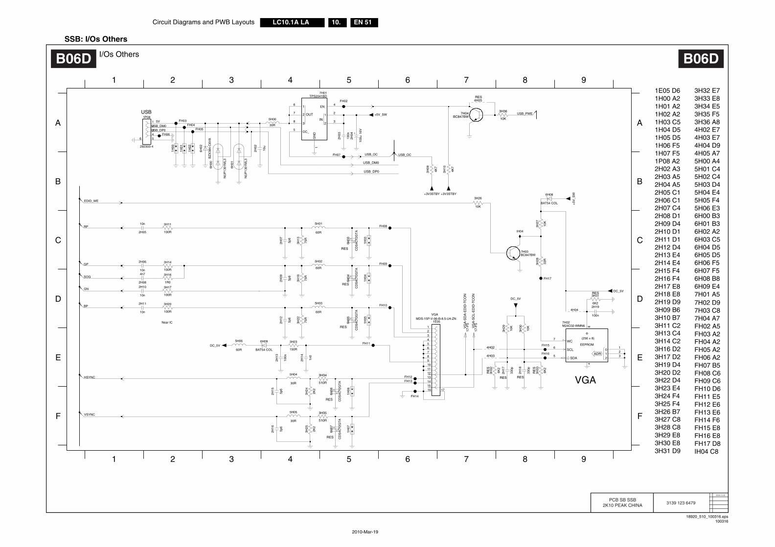
Circuit Diagrams and PWB Layouts EN 51LC10.1A LA 10.
2010-Mar-19
SSB: I/Os Others
18920_510_100316.eps100316
I/Os OthersB06D B06D
2009-12-301
3139 123 6479PCB SB SSB
2K10 PEAK CHINA
1
2IN
1
2
3
OUT
SCLADR
012SDA
WC
2H04 A52H05 C1
IH04 C8
VGA
5H03 D4
4H05 A7
8
3H09 B63H10 B7
5H00 A45H01 C4
FH07 B5FH08 C6FH09 C6FH10 D6
7H03 C8
FH11 E5FH12 E6FH13 E6FH14 F6FH15 E8FH16 E8
4H03 E74H04 D9
FH06 A2
976
1
3H11 C2
5H06 E3
5H02 C4
3H13 C4
6H00 B36H01 B3
5H04 E45H05 F4
6H05 D5
Near IC
2H03 A5
1H03 C5
2H06 C1
2H17 E87H01 A57H02 D9
7H04 A7FH02 A5FH03 A2FH04 A2FH05 A2
4H02 E7
FH17 D8
VGA
5
9
A
B
2
3H26 B73H27 C8F
6H02 A26H03 C56H04 D5
6H09 E4
3H28 C8
E
A
1H01 A21H02 A2
2H13 E42H14 E42H15 F42H16 F4
3H32 E73H33 E83H34 E53H35 F53H36 A8
2H19 D9
2H08 D12H09 D42H10 D1
1P08 A22H02 A3
1H05 D5
3
1 2 3 4
USB
7 8
3H22 D43H23 E43H24 F43H25 F4
3H17 D23H19 D43H20 D2
6H06 F56H07 F56H08 B8
4 5 6
1H06 F51H07 F5
2H18 E8
1H04 D5
3H14 C23H16 D2
B
C
D
E
F
1E05 D61H00 A2
2H11 D12H12 D4
3H29 E83H30 E83H31 D9
C
D
2H07 C4
330p
2H17
RES
3H24
2K2
BC847BW7H04
4EN_
GN
D1
2
3
OC_5
6
7
8
+3V3STBY
TPS2041BD7H01
FH14
1H02
5H01
60R
2H13
100n
FH02
FH05
4H04
1715
23456789
16
MDS-15P-V-06-B-8.5-U4-ZN1E05
1
1011121314
2H16
5p6
2H05
10n
CD
S4C
12G
TA
RES
6H06
FH17
FH08
4H02
2H18
330p
RES
2H02
10u
IH04
RES4H05
5H05
1H06
30R
2H10
10nDC_5V
2H15
5p6
23
6
5
84
7 (256 × 8)
Φ
EEPROM
7H02M24C02-WMN6
1
DC_5V
RES
CD
S4C
12G
TA
6H04
2H12
5p6
3H20
100R
10K
3H29
DC_5V
1n0
2H14
100R
1H01
10n
2H06
3H11
+3V3STBY
10K
3H36
1H07
RE
S
6K2
3H33
30R
5H00
FH10
+5V
_SW
BAT54 COL
6H08
510R
3H35
1H00
FH07
2H11
10n2K
2
3H25
2H07
5p6
60R
5H06
3H09
4K7
6H07
RES CD
S4C
12G
TA
CD
S4C
12G
TA
6H05
RES
FH15
5p6
2H09
1H05
FH16
1H03
2H04
100u
16V
FH06
17-F
5
17-F
5
FH09
3H30
10K
6H09
BAT54 COL
4K7
3H10
10K
3H27
3H26
10K
FH12
NU
P13
01M
L3
6H00
NU
P13
01M
L3
6H01
RES
6K2
3H31
5H02
60R
5H03
60R
6H02
+5V_SW
BZ
X38
4-C
6V8
2H08
4n7
510R
3H34
FH13
3H14
100R
5H04
1H04
30R
2H19
100n
6K2
3H32
RE
S
3H23
150R
1R0
3H16
RES CD
S4C
12G
TA
6H03
FH11
75R
4H03
3H22
FH03
2H03
FH04
100n
3H28
33R
100R
3H17
3H13
75R
456
75R
3H19
1P08
292303-4
123
7H03BC847BW
VG
A-S
DA
-ED
ID-T
CO
N
VG
A-S
CL-
ED
ID-T
CO
N
USB_PWE
USB_OC
USB_DM0
USB_DM0
USB_DP0
USB_DP0
HSYNC
VSYNC
GN
RP
SOG
GP
BP
5V
USB_OC
EDID_WE

EN 52LC10.1A LA 10.Circuit Diagrams and PWB Layouts
2010-Mar-19
SSB: DC-DC & Power 8282
18920_511_100316.eps100319
DC-DC & Power MT8282B07A B07A
2009-12-301
3139 123 6479PCB SB SSB
2K10 PEAK CHINA
2J16 C2
3J11 D113J12 D11
FJ10 G8FJ11 F10FJ12 C7
2J55 D7
3J06 D7
2J71 C2
2J72 C2
FJ19 G9
3J33 E73J34 D8
3J07 E73J08 E7
3J35 E82J31 D22J32 D2
FJ18 E8
FJ08 F8
2J33 D22J34 D3
5J05 E25J06 E2
2J51 B10
2J13 B42J14 B42J15 B4
2J56 D82J57 G3
3J13 E83J14 E113J15 E113J16 E11
FJ13 D6FJ14 D8
2J52 B102J53 B112J54 B11
3J27 G83J28 F93J29 G93J30 C73J31 C7
2J30 D2
2J35 D32J36 D3
2J73 C22J74 C32J75 C32J76 C3
2J68 E32J69 B22J70 C2
3J36 F73J37 E75J02 A10
7J03 F9FJ01 B2FJ02 A11FJ05 D6FJ06 A3FJ07 F8
FJ09 F8
5J04 E2
2J12 B3
2J17 C22J18 C2
2J58 G32J59 G32J60 G32J61 G3
FJ15 D9FJ16 D8
2J06 A4
2J37 D32J38 D32J39 D32J40 D3
5J07 F25J08 F25J09 F25J10 F25J11 F2
5J14 A10
FJ17 E8
2J50 B10
2J19 C22J20 C32J21 C32J22 C3
3J17 E113J18 D83J19 D8
IJ09 D8IJ10 D7
2J29 C4
2J02 B32J03 A32J04 A42J05 A4
2J77 C32J78 C32J79 C3
5J12 G25J13 A2
7J01-4 D97J01-5 A5
2J07 B32J08 B32J09 B32J10 B32J11 B3
1J04 C72J01 B2
2J62 G32J63 G42J64 G4
3J22 G73J23 E83J26 F8
2J28 C4
2J41 D42J42 D42J43 D4
2J80 C32J81 C43J05 D8
1J01 D8
2J44 E42J45 E42J46 E4
2J23 C32J24 C32J25 C3
2J65 G42J66 F92J67 E3
2J26 C32J27 C4
DU
VCC
Q
VSS
D
C
S
W
HOLD
DMPLL
AVDD12
AVDD33
AVSS12
VPLL
AVSS33
XTAL
LVDSB_4LVDSB_3LVDSB_2LVDSB_1
LVDSA_2LVDSA_1
VPLL
LVDS
MEMPLL
MJCPLLDMPLL
SYSPLL
LVDSRX_CKLVDSRX
LVDSRX_1LVDSRX_2
DVSS
VCC2IO
XTAL
LVDSB_2LVDSB_1
LVDSA_2LVDSA_1
VCCK
LVDSRXELVDSRXO
LVDSRXLVDSRX_CK
SYSPLL
MJCPLL
MEMPLL
LVDS
SCLSDA
SFD0SFD1
TP0TN0
0123
GPIO
JRTCKJTCKJTDIJTDOJTMSJTRST
XTALIXTALOEFUSEPRSTRXD0RXDMA_ACK
CLK_INCLK_OUT
SFCKSFCSTXD0
MEMTNMEMTP
NC
6
NC
1
NC
H
NC
G
7 8
NC
2 3
A
B
9 10 11 12
NC
4 5 6 7
3 4 52
C
D
E
F
G
H
DNC
NC
E
F
8 11 12
NC
1
9 10
100n
A
B
C2J
28
3J06 1R0
2J40
100n
2J13
100n
100n
2J39
100n
2J10
2J51
22u
100n
2J79
5J11 30R
5J10 30R
5J13
30R
1K03J22
100n
2J72
3J37
2J42
100n
1K0
100n2J66
100n
2J37
2J62
100n
FJ01
FJ07
FJ09
+3V3_SW
4u7
2J30
2J63
100n
100n
2J23
2J80
100n
2J55 27p
9
2J11
100n
11121314
1
8
7
210
16
15
3456
+3V3_SW
+3V3_SW
Φ2M × 8FLASH
M25P16-VMF7J03
4K7
3J18
FJ06
1R03J17
100n
2J29
1K0
3J28
RE
S
+3V3_SW
4K7
3J31
100n
2J14
100n
2J74
3J19
4K7
100R 3J13
2J16
100n
100n
2J81
2J46
100n
2J76
100n
100n
2J25
100n
2J45
100n
2J19
3J12 1R0
100n
2J57
30R5J09
4u7
2J67
4K7
3J30
+3V3_SW
2J71
100n
C19
B19C20
W18Y18
Y17
W19W20
U3U4
A1A2
W2W17W1
V11U11
B20Y16
Y2
V3Y3W3V4U2V2V1T5
D16
PHERIPHERAL
7J01-4MT8282
W16
A19
M12N8N10N13
A20B17B18C16C17D15
E14E15H10H12J9J11J13L8L13M9
C9C15D8D14E7E8
C18R5T4U12
A18
P4P5R2R3R4T1T2T3U1
B16
E9E13F1F2F3G4G5L5N5P3
B8
N11N12T12U5V5
C12C13D4
D11E5
A17
L10L11L12M8
M10M11M13
N3
C11
N9
K4K5K8K9
K10K11K12K13
C4
L3L9
E11F16H5H9
H11H13
J3J5
C3
J10J12
R16T16V16V19
V6V10
Y19
B2
E6E10
V20
V14
L18
V8V7
J8
V15
V13
L17
H16J16
H8
U15
U13
L19
K17K18
U16V17
U10U6
POWERMT82827J01-5
U14
K19
U8U7
100n
2J43
2J09
100n
2J02
4u7
+3V3_SW
2J54
22u
22u
2J53
100n
2J12
+1V1_8282
2J05
100n
2J07
100n
100n
2J35
2J65
100n
+3V3_SW
2J52
220u
6.3V
100n
2J77
2J58
100n
2J73
100n
100n
2J33
5J07 30R
22u
2J50
2J26
100n
IJ10
1K0
3J23
100n
2J75
2J32
100n
FJ10
30R5J06
1R03J11
5J08 30R
2J68
4u7
+1V8_DDR2
2J01
6.3V100u
100n
2J61
100n
2J27
FJ17
FJ16
FJ15
FJ13
3J34 1R0
34
56
RES
1J04
502382-0470
12
RE
S
1K0
3J29
3J08 1R0
100R3J07
2J60
100n
FJ05
820K3J05
1J01322527M
2J70
100n
2J03
100n
5J14
33R
2J38
100n
3J33
+1V1_SW
5J02
33R
1R0
6-F3
2J78
100n
+3V3_SW
27p2J56
FJ18
FJ19
5J05 30R
30R5J04
2J15
100n
+3V3_SW
FJ12
FJ14IJ09
+1V2_SW
22u
2J69
1K0
3J26
RE
S
100n
2J08
2J24
100n
3J16 1R01R03J15
3J14 1R0
2J06
3J35
10K
100n
100n
2J04
2J44
100n
2J34
100n
2J22
100n
100n
2J17
RE
S
RE
S
3J36
1K0
1K0
3J27
100n
2J59
+3V3_SW
FJ11
FJ02
2J36
100n
100n
2J41
FJ08
30R5J12
+1V1_8282
2J18
100n
100n
2J21
2J20
100n
100n
2J31
100n
2J64
MJC_ACK_COMMMJC_UoRX
MJC_DEBUG_RXMJC_DEBUG_TX
AV12_PLL
AV33_LVDSRx
AV12_LVDSVPLL
AV12_LVDSTx
AV33_XTAL
AV12_MEMPLL
AV12_LVDSRxCKAV12_LVDSRx
SPI_SCK
SPI_SO SPI_SI
SPI_CS#
AV33_LVDSTx
MJC_UoTX
SPI_SCKSPI_CS#
U2RXSCLSDA
SPI_SOSPI_SI
MJC_RST#
U2TX
MJC_RXDMA_ACK
8282_XTALO8282_XTALI
B04C
B04C
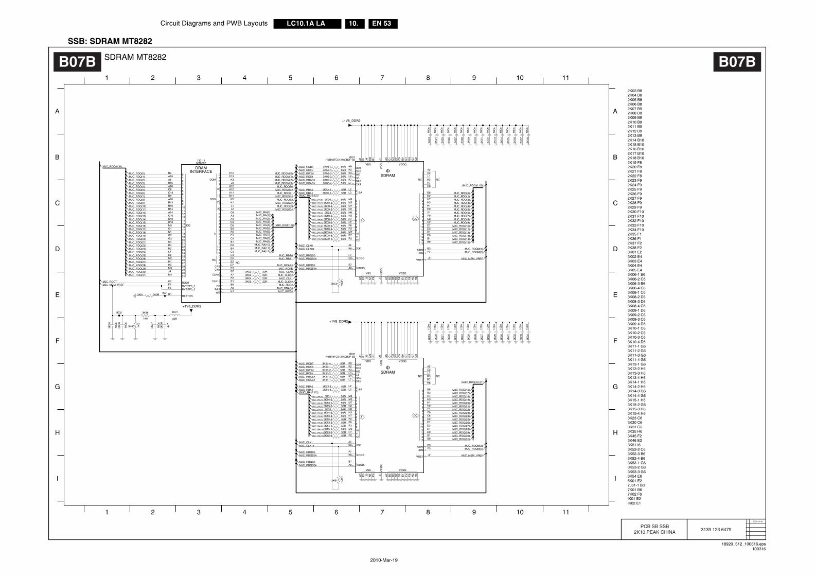
Circuit Diagrams and PWB Layouts EN 53LC10.1A LA 10.
2010-Mar-19
SSB: SDRAM MT8282
18920_512_100316.eps100316
SDRAM MT8282B07B B07B
2009-12-301
3139 123 6479PCB SB SSB
2K10 PEAK CHINA
121110
9876543
0123456789101112
CK
VD
DL
VREF
VS
SD
L
14
VDDQ
QSSVSSV
BA
A
LDQS
UDQS
NC
DQ
CKEWE
ODT
RAS
1
CS
CAS
0012
VDD
LDMUDM
15
13
56789
012
CASCKE
CLK0
CSRASWE
A
BA
CLK1
REXTDN
RVREF0_2RVREF0_1RODT
1819202122232425262728293031
DQM
0
1
2
3
DQS
0123
01
101112
234
DQ
01234567891011121314151617
121110
9876543
0123456789101112
CK
VD
DL
VREF
VS
SD
L
14
VDDQ
QSSVSSV
BA
A
LDQS
UDQS
NC
DQ
CKEWE
ODT
RAS
1
CS
CAS
0012
VDD
LDMUDM
15
13
3K46 E23K51 I63K52-2 C63K52-3 B63K52-4 B6
NC
7K02 F6IK01 E2IK02 E1
7K01 B6
NC
NC
3K53-2 G6
3K54 E65K01 E27J01-1 B3
3K14-1 H63K14-2 H63K14-3 G63K14-4 G63K15-1 H6
2K38 F23K01 E23K02 E43K03 E4
3K15-3 H6
3K23 C6
3K31 G63K35 H63K45 F2
3K09-2 C63K09-3 C63K09-4 D63K10-1 C63K10-2 C63K10-3 C63K10-4 D6
3K11-2 G6
3K53-1 G6
3K11-4 G6
3K53-3 G6
3K13-2 H63K13-3 H63K13-4 H6
2K33 F102K34 F102K35 F12K36 F12K37 F2
3K04 E43K05 E43K06-1 B6
3K15-2 G6
3K06-3 B6
3K15-4 H6
3K08-1 C6
3K30 C6
3K08-3 D63K08-4 C63K09-1 D6
2K17 B102K18 B102K19 F82K20 F82K21 F8
8 9 10
2K22 F82K23 F92K24 F9
3K11-1 G6
2K26 F9
3K11-3 G6
2K28 F9
3K13-1 G6
2K30 F102K31 F102K32 F10
B
C
D
E
F
2K06 B82K07 B9
1 2
3K06-2 C6
2K10 B9
3K06-4 C6
2K12 B9
3K08-2 D6
2K14 B102K15 B102K16 B10
3 4 5 6 7 11
A
B
2K25 F9
D
2K27 F9
F
2K29 F9
H
I
A
G
H
I
2K03 B82K04 B82K05 B8
2K08 B92K09 B9
3 4
2K11 B9
5
2K13 B9
6 7 8 9 10 11
1 2
C
E
G
56R3K11-4
56R3K06-2
100n
2K07
100R
3K54
100n
56R3K15-2
2K24
56R3K13-3
56R3K13-456R3K14-2
100n
56R3K15-1
2K14
100n
2K30
56R3K14-3
2K29
100n
56R3K11-1
100n
2K28
56R3K53-2
56R3K08-4
56R3K11-2
56R3K52-4
2K23
100n
56R3K09-1
100n
2K22
56R3K09-4
2K27
100n
56R3K09-3
56R3K3056R3K10-2
56R3K06-3
56R3K08-1
3K23 56R
IK01
22R3K05
22R3K03
56R3K53-3
2K08
100n
3K52-2 56R
100n
2K13
100n
2K05
56R3K52-3
+1V8_DDR2
2K06
100n
3K13-2
2K33
100n
56R
3K15-3 56R
100n
2K32
100n
2K34
3K51 100R
100n
2K09
56R3K10-1
56R3K06-4
2K25
100n4u
7
2K38
2K04
100n
100n
2K03
1K0
3K45
3K01 300R
100n
2K26
100n
2K15
3K10-3 56R
56R3K14-1
22R3K02
2K31
100n
56R3K11-3
5K01
30R
22R3K04
56R3K53-1
3K06-1 56R
56R3K08-3
2K21
100n
56R3K08-2
2K16
100n
2K12
100n
100n
2K11
2K10
100n
3K14-4 56R
+1V8_DDR2
100n
2K37
D8
E7
F2
F8
H2
K3
E3 J3 N1
P9 J7 A7
H8
B2
B8
D2
G9
C1
C3
C7
C9
E9
G1
G3
G7
J2
A3
B7A8
A1
E1
J9 M9
R1
J1 A9
E8
A2E2L1R3R7R8
K9
K7
B3
H7H3H1H9F1F9C8C2
F3F7
K2
K8
L8
G8G2
D7D3D1D9B1B9
N2N8N3N7P2P8P3
L2L3
L7
J8
7K01HYB18TC512160B2F-3S
M8M3
M2P7R2
M7
2K35
SDRAMΦ
100n
56R3K15-4
56R3K35
56R3K13-1
56R3K31
56R3K10-4
56R3K09-2
L2
R1
C7
A6F4F5
E1
E12D13
K3J2
B12A12A11B11K2K1L1
H3M3
B15
J4M4
A16C8C14D9A10B13
G2
A8
G3N4H4N2L4H2M2H1
B9A15
B10B14A14C10D12D10M5G1N1
B1
E4D5E2D7E3B7A7P2P1B6
D2B4C2
A4D3D6B3B5C1C5
INTERFACEDRAM
7J01-1MT8282
C6A3
100n
2K20
+1V8_DDR21K0
3K46
100n
2K36
100n
2K17
IK02
100n
2K18
2K19
100n
H8
B2
B8
D2
D8
E7
F2
F8
H2
K3
G1
G3
G7
J2
A3
E3 J3 N1
P9 J7 A7
M9
R1
J1 A9
G9
C1
C3
C7
C9
E9
R8
K9
K7
B3
B7A8
A1
E1
J9
F9C8C2
F3F7E8
A2E2L1R3R7
D3D1D9B1B9
H7H3H1H9F1
P3
L2L3
L7
J8
K2
K8
L8
G8G2
D7
M2P7R2
M7N2N8N3N7P2P8
Φ
7K02
SDRAM
HYB18TC512160B2F-3S
M8M3
MJC_RDQM(1)
MJC_RDQM(3)MJC_RDQM(2)
MJC_RBA0MJC_RBA1
MJC_RCAS#MJC_RCKEMJC_CLK0
MJC_CLK0#MJC_CLK1
MJC_CLK1#MJC_RCS#
MJC_RRAS#MJC_RWE#
MJC_RA(11)MJC_RA(12)
MJC_RDQS3MJC_RDQS3#
MJC_RDQS2MJC_RDQS2#
MJC_RDQS0MJC_RDQS0#MJC_RDQS1
MJC_RDQS1#
MJC_RDQM(0)
MJC_RDQ(0:31)
{MJC_RA(0:12)}
MJC_RA(0)MJC_RA(1)MJC_RA(2)MJC_RA(3)MJC_RA(4)MJC_RA(5)MJC_RA(6)MJC_RA(7)MJC_RA(8)MJC_RA(9)
MJC_RA(10)MJC_RDQ(21)MJC_RDQ(22)MJC_RDQ(23)MJC_RDQ(24)MJC_RDQ(25)MJC_RDQ(26)MJC_RDQ(27)MJC_RDQ(28)MJC_RDQ(29)MJC_RDQ(30)MJC_RDQ(31)
MJC_RDQ(10)MJC_RDQ(11)MJC_RDQ(12)MJC_RDQ(13)MJC_RDQ(14)MJC_RDQ(15)MJC_RDQ(16)MJC_RDQ(17)MJC_RDQ(18)MJC_RDQ(19)MJC_RDQ(20)
MJC_RDQ(0)MJC_RDQ(1)MJC_RDQ(2)MJC_RDQ(3)MJC_RDQ(4)MJC_RDQ(5)MJC_RDQ(6)MJC_RDQ(7)MJC_RDQ(8)MJC_RDQ(9)
MJC_RDQS2MJC_RDQS2#
MJC_RDQS3MJC_RDQS3#
MJC_RDQM(3)MJC_RDQM(2)
MJC_MEM_VREF
MJC_RCKEMJC_RWE#
MJC_RRAS#MJC_RCAS#
MJC_RCS#
MJC_RBA0MJC_RBA1
MJC_CLK1MJC_CLK1#
MJC_RA(6)
MJC_RA(7)
MJC_RA(8)
MJC_RA(9)
MJC_RA(10)
MJC_RA(11)
MJC_RA(12)
MJC_RODT
MJC_RDQ(25)MJC_RDQ(26)MJC_RDQ(27)MJC_RDQ(28)MJC_RDQ(29)MJC_RDQ(30)MJC_RDQ(31)
{MJC_RA(0:12)}
MJC_RA(0)
MJC_RA(1)
MJC_RA(2)
MJC_RA(3)
MJC_RA(4)
MJC_RA(5)
MJC_RODTMJC_RCKEMJC_RWE#
MJC_RRAS#MJC_RCAS#
MJC_RCS#
MJC_RBA0MJC_RBA1
{MJC_RDQ(16:31)}
MJC_RDQ(16)MJC_RDQ(17)MJC_RDQ(18)MJC_RDQ(19)MJC_RDQ(20)MJC_RDQ(21)MJC_RDQ(22)MJC_RDQ(23)MJC_RDQ(24)
MJC_RA(4)
MJC_RA(5)
MJC_RA(6)
MJC_RA(7)
MJC_RA(8)
MJC_RA(9)
MJC_RA(10)
MJC_RA(11)
MJC_RA(12)
{MJC_RDQ(0:15)}
MJC_RDQ(5)MJC_RDQ(6)MJC_RDQ(7)MJC_RDQ(8)MJC_RDQ(9)
MJC_RDQ(10)MJC_RDQ(11)MJC_RDQ(12)MJC_RDQ(13)MJC_RDQ(14)MJC_RDQ(15)
{MJC_RA(0:12)}
MJC_RA(0)
MJC_RA(1)
MJC_RA(2)
MJC_RA(3)
MJC_MEM_VREF
MJC_RODTMJC_MEM_VREF
MJC_CLK0MJC_CLK0#
MJC_RDQ(0)MJC_RDQ(1)MJC_RDQ(2)MJC_RDQ(3)MJC_RDQ(4)
MJC_RDQM(0)MJC_RDQS0MJC_RDQS0#
MJC_RDQM(1)
MJC_RDQS1MJC_RDQS1#
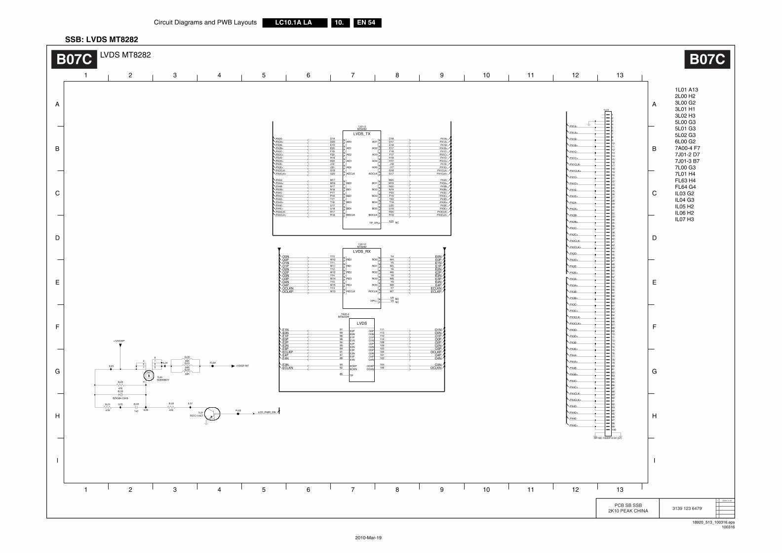
EN 54LC10.1A LA 10.Circuit Diagrams and PWB Layouts
2010-Mar-19
SSB: LVDS MT8282
18920_513_100316.eps100316
LVDS MT8282B07C B07C
2009-12-301
3139 123 6479PCB SB SSB
2K10 PEAK CHINA
PRECLK ROCLK
NP
VIPLL
PNP
RE0 RO0
NP
NP
RE1 RO1
NP
NP
RE2 RO2
NP
NP
RE3 RO3
NP
NP
RE4 RO5
NP
N
N
O1NO2PO2NO3PO3NO4PO4N
OCKPOCKN
E0PE0NE1PE1NE2PE2NE3PE3NE4PE4N
ECKPECKN
TP
O0PO0NO1P
NP
BO3
NP
BO4
NP
BO5
NP
BOCLK
TP_VPLL
PAO4
NP
AO5
NP
AOCLK
NP
BE0
NP
BE1
NP
BE2
NP
BE3
NP
BE4
NP
BECLK
NP
BO1
NP
BO2
NP
AE0
NP
AE1
NP
AE2
NP
AE3
NP
AE4
NP
AECLK
NP
AO1
NP
AO2
NP
AO3
N
H
8 9 10 11 12
NCNC
11 12
1
2L00 H23L00 G23L01 H1
1L01 A13
3
I
G
7
E
IL03 G2
134 5 6
2 3
2
D
IL06 H2IL07 H3
IL04 G3IL05 H2
G
H
4 5
FL64 G4
NC
F
A
B
C
I
10
6L00 G27A00-4 F7
5L01 G35L02 G3
7L01 H4FL63 H4
C
D
E
6
B
A
7J01-3 B77L00 G3
13
1 7
3L02 H35L00 G3
F
8 9
7J01-2 D7
99
9
909192939495969798
79
8
80818283848586878889
7
707172737475767778
60616263646566676869
5
50515253545556575859
6
40414243444546474849
30313233343536373839
4
212223242526272829
3
111213141516171819
2
20
DF18C-100DP-0.5V (51)
1L01
1
10
100
123
SI4835BDY
5678
4
+VDISP-INT
7L00
Y9W9Y7W7
U9V9
W15Y13W13
Y4W4Y5W5Y6W6Y8W8
Y10W10Y11W11Y12W12Y14W14Y15
LVDS_RX
7J01-2MT8282
IL03 30R
5L01 FL64
47K
3L00
5L00
30R
BZX384-C6V8
6L00
PDTC114ET
FL637L01
IL07
IL04
IL06
+12VDISP
47K
3L02IL05
1u0
2L003L01
47R
30R
U19R20R19
K20
5L02
R17R18
M20M19N20N19P20P19T20T19U20
G17
M17M18N17N18P17P18T17T18U17U18
D17E18E17F18F17H18H17J18J17G18
E19E20F19F20H19H20J19J20G19G20
D18
7J01-3MT8282
LVDS_TXD19D20
103
102101
106104
86
8887
9290
113111
112110
109108
105
LVDS
9997
9896
9594
9189
MT8222R7A00-4
PX1A-
PX1C-
PX1C+
PX1A+
PX1B-
PX1B+
PX2A-
PX2A+
PX2B-
PX2B+
PX2C-
PX2C+
PX1CLK-
PX1CLK+
PX1D-
PX1D+
PX1E-
PX1E+
PX3A-
PX3A+
PX3B-
PX3B+
PX3C-
PX3C+
PX2CLK-
PX2CLK+
PX2D-
PX2D+
PX2E-
PX2E+
PX4A-
PX4A+
PX4B-
PX4B+
PX4C-
PX4C+
PX3CLK-
PX3CLK+
PX3D-
PX3D+
PX3E-
PX3E+
PX4E-
PX4E+
PX4CLK-
PX4CLK+
PX4D-
PX4D+
O0N
OCLKNO4PO4NO3PO3NO2PO2NO1PO1NO0P
PX2A-
ECLKPECLKN
E4PE4NE3PE3NE2PE2NE1PE1NE0PE0N
OCLKP
PX2E-PX2D+PX2D-PX2C+PX2C-PX2B+PX2B-PX2A+
PX1C-PX1B+PX1B-PX1A+PX1A-
PX2CLK+PX2CLK-PX2E+
PX4B-PX4A+PX4A-
PX1CLK+PX1CLK-
PX1E+PX1E-
PX1D+PX1D-PX1C+
PX4CLK-PX4E+PX4E-PX4D+PX4D-PX4C+PX4C-PX4B+
PX3D-PX3C+PX3C-PX3B+PX3B-PX3A+PX3A-
PX4CLK+
E0P
E1NE0N
PX3CLK+PX3CLK-
PX3E+PX3E-
PX3D+
E4N
E3PECLKP
E2PE2N
E1P
OCLKP
O2PO2N
O1PO0P
O1NO0N
E3NECLKN
E4P
LCD_PWR_ON
O3NOCLKN
O4PO4N
O3P
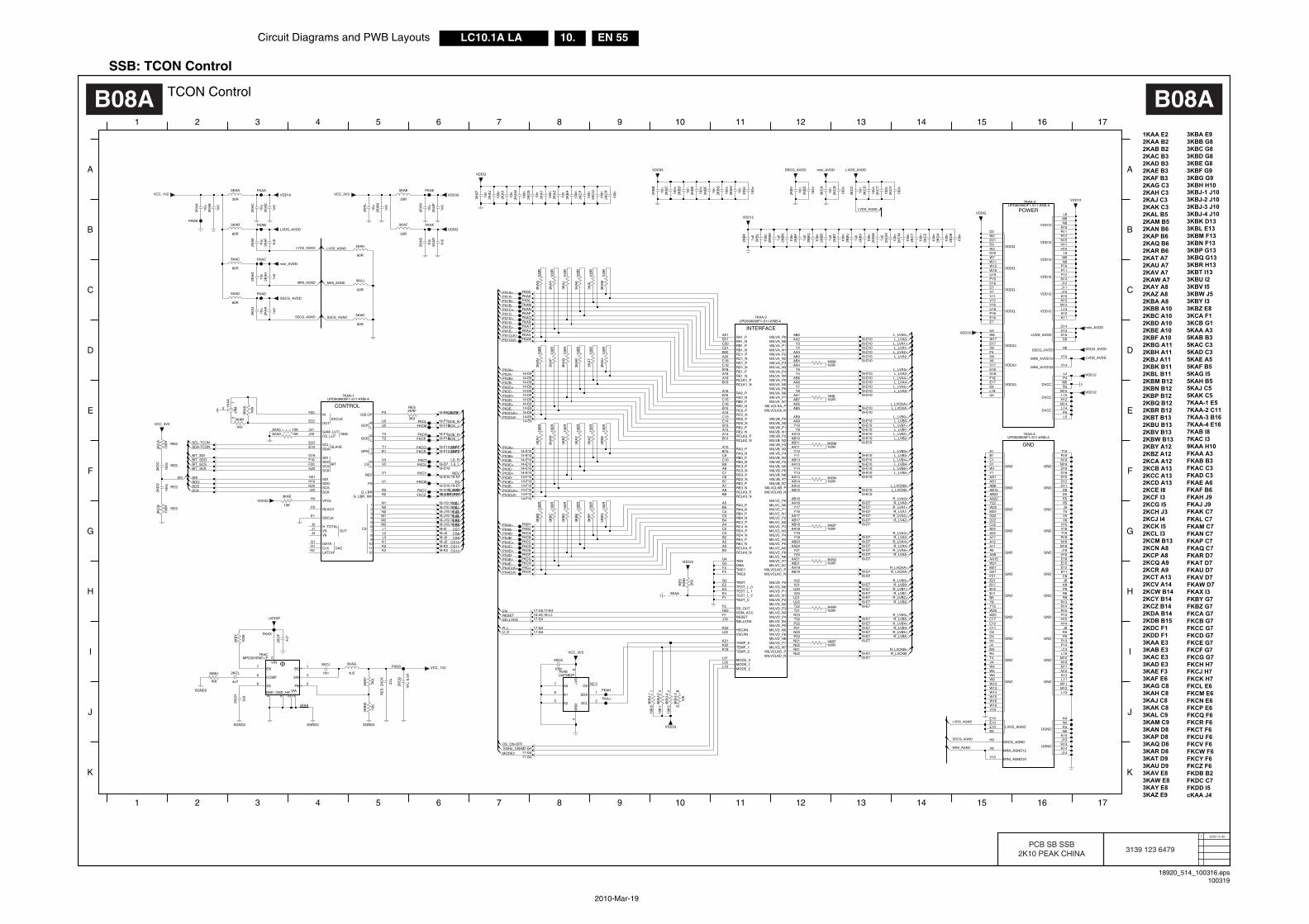
Circuit Diagrams and PWB Layouts EN 55LC10.1A LA 10.
2010-Mar-19
SSB: TCON Control
18920_514_100316.eps100319
TCON ControlB08A B08A
2009-12-301
3139 123 6479PCB SB SSB
2K10 PEAK CHINA
2KBA A82KBB A102KBC A10
1KAA E2
2KAW A7
2KAC B3
2KDB B152KDC F12KDD F1
2KBG A112KBH A112KBJ A11
2KAN B62KAP B6
2KBZ A122KCA A122KCB A132KCC A132KCD A13
3KAT D93KAU D93KAV E8
2KCF I32KCG I52KCH J3
2KAA B2
2KCE I8
2KAY A82KAZ A8
2KAL B52KAM B5
2KAU A72KAV A7
2KCZ B142KDA B14
3KBK D133KBL E133KBM F13
3KAA E33KAB E33KAC E3
2KBD A102KBE A102KBF A10
2KAT A7
3KAR D8
3KAW E83KAY E83KAZ E9
2KAE B32KAF B32KAG C32KAH C3
2KAB B2
FKAQ C7FKAR D7FKAT D7
3KBN F133KBP G133KBQ G13
2KBK B112KBL B11
2KAQ B62KAR B6
2KBW B13
FKCR F6FKCT F6FKCU F6
5KAD C35KAE A55KAF B5
2KCJ I42KCK I5
2KAD B3
2KAJ C32KAK C3
2KCW B14
FKAB B3FKAC C3FKAD C3FKAE A6
FKAJ J9FKAK C7FKAL C7FKAM C7FKAN C7FKAP C7
FKAW D7FKAX I3FKBY G7FKBZ G7FKCA G7FKCB G7
3KAD E33KAE F3
2KBP B12
3KAP D8
2KBY A12
FKCC G7FKCD G7FKCE G7FKCF G7FKCG G7
FKCK H7FKCL E6FKCM E6FKCN E6FKCP E6FKCQ F6
5KAC C3
5KAG I55KAH B55KAJ C55KAK C57KAA-1 E5
3KBA E93KBB G8
2KCN A8
3KBJ-1 J10
2KCT A13
3KBJ-2 J103KBJ-3 J10
2KCY B14
7KAC I39KAA H10
3KBJ-4 J10
FKAF B6FKAH J9
7KAA-2 C117KAA-3 B167KAA-4 E167KAB I8
FKAU D7FKAV D7
FKDC C7FKDD I5cKAA J4
3KBR H133KBT I133KBU I23KBV I5
3KAM C9
2KBM B122KBN B12
3KAH C8
2KBQ B122KBR B122KBT B13
2KBV B13
3KBW J5
3KAJ C83KAK C83KAL C9
2KBU B13
3KAN D8
3KBC G83KBD G8
3KBF G93KBG G93KBH H10
FKCH H7FKCJ H7
3KBY I33KBZ E83KCA F13KCB G1
FKAA A3
FKCV F6FKCW F6FKCY F6FKCZ F6FKDB B2
2KCL I32KCM B13
3KBE G8
2KCP A82KCQ A92KCR A9
2KCV A14
5KAA A35KAB B3
3KAQ D8
3KAF E63KAG C8
MINI_AGND12
SSCG_AGND
GND
LVDS_AGND
GND
GND
GND
GND
GND
GND
GND
GND
GND
DGND
DGND
GND
GND
GND
GND
GND
GND
GND
GND
GND
GND
GND
GND
MINI_AGND34
GND VIAGND_HS
SWCOMP
EN
VIN
SS FB
BS
MILVC_N3MILVC_P4MILVC_N4MILVC_P5MILVC_N5MILVC_P6MILVC_N6MILVC_P7MILVC_N7
MILVCLKC_PMILVCLKC_N
MILVD_P0MILVD_N0MILVD_P1MILVD_N1MILVD_P2MILVD_N2MILVD_P3MILVD_N3MILVD_P4MILVD_N4MILVD_P5MILVD_N5MILVD_P6MILVD_N6MILVD_P7MILVD_N7
MILVCLKD_PMILVCLKD_N
MILVA_N5MILVA_P6MILVA_N6MILVA_P7MILVA_N7
MILVCLKA_PMILVCLKA_N
MILVB_P0MILVB_N0MILVB_P1MILVB_N1MILVB_P2MILVB_N2MILVB_P3MILVB_N3MILVB_P4MILVB_N4MILVB_P5MILVB_N5MILVB_P6MILVB_N6MILVB_P7MILVB_N7
MILVCLKB_PMILVCLKB_N
MILVC_P0MILVC_N0MILVC_P1MILVC_N1MILVC_P2MILVC_N2MILVC_P3
MILVA_P0MILVA_N0MILVA_P1MILVA_N1MILVA_P2MILVA_N2MILVA_P3MILVA_N3MILVA_P4MILVA_N4MILVA_P5
RC4_PRC4_NRD4_PRD4_NRE4_PRE4_NRCLK4_PRCLK4_N
TENDMATMC1TMC2
TRSTTEST_L_0TEST_L_1TEST_L_2TEST_C
SS_OUTROM_ACCRESETSELLVDS
HSCANVSCAN
TEMP_0TEMP_1TEMP_2
MODE_0MODE_1MODE_2
RE1_PRE1_NRCLK1_PRCLK1_N
RA2_PRA2_NRB2_PRB2_NRC2_PRC2_NRD2_PRD2_NRE2_PRE2_NRCLK2_PRCLK2_N
RA3_PRA3_NRB3_PRB3_NRC3_PRC3_NRD3_PRD3_NRE3_PRE3_NRCLK3_PRCLK3_N
RA4_PRA4_NRB4_PRB4_N
RA1_PRA1_NRB1_PRB1_NRC1_PRC1_NRD1_PRD1_N MINI_AVDD34
MINI_AVDD12
VDD12
SSCG_AVDD
DVCC
DVCC
VDD12
LVDS_AVDD
DVCC
VDD12
VDD12
VDD12
VDD12
VDDQ
VDDQ
VDD33
VDD33
VDD33
VDDQ
VDDQ
789
101112
VSV8
DATACLKLATCH
IN
OUT
GAM_LUTOS_LUT
SCLSDA
SDISDOSCSSCK
SDISDOSCSSCK
VPOL
READY
SSCLK
H_TOTAL
EXCLK
DBG
SLAVE
BIT
OUT
DAC
CS
GCK
RL
GCE
12
GPS
RL
LS
GSLOP
RL
321
G_LBR_INVG_LBR
FS
REV
456
2
F
5 6 73 4
17
8 9 10 11 12
G
17
A
B
13 14
6 73 4 51 15
E
C
D
15 16
C
D
A
NC
1 2
16
H
G
I
J
K
B
8 9 10 11 12 14
E
F
H
I
J
13
K
2KB
A
100n
2KB
R
1u0
1u0
2KB
P
VDDQ
1n0
2KA
R
2KA
Q
10u
3KBP100R
24M1K
AA
2
13
100R
3KA
T
3KA
R10
0R
100R
3KA
G
mini_AVDD
2KC
C
10n
3KAD 10K10K3KAC
2KB
G
100n
FKCK
FKCD
FKAK
FKCJ
60R
5KAJ
10n
2KB
H
2KB
F
10n
100R
3KA
M10
0R
3KA
V
10n
2KA
T
FKAD
2KA
G
5KAC10
u
60R
10n
2KC
A
SSCG_AVDD
3KB
D10
0R
100R
3KB
C
LVDS_AVDD
5KAD
60R
1n0
2KA
F
5KAH
60R
VDD33
2KC
R
100n
2KA
P
1n0
VDD33
10n
2KB
D
100n
2KB
E
2KB
C
100n
2KC
D
100n
100n
2KD
D
RES
RES
RES
2KD
C
100n
3KC
A
100R
3KB
V
7K5
100n
2KA
U
2KA
Z
10n
5KAK
60R
SSCG_AVDD
2KA
V
10n
2KB
N
100n
3KB
A10
0R
3KA
Z10
0R
3KA
N10
0R
100n
2KA
Y
2KA
W
100n
2KB
M
1u0
1u0
2KB
K
VDD33
FKCG
3KB
J-4
45
VDD33
FKCE
3KBR
10K
100R
3KBT100R
FKAV
3KA
W10
0R
LVDS_AVDD
2KB
Z
100n
100n
2KC
M
100n
2KC
Q
2KC
P
100n
10u
2KA
N
VDDQ
2KB
B
10n
1n0
2KA
Hmini_AVDD
100R
3KB
F
3KB
E10
0R
3KA
Q
3KA
P
100R
100R
10n
2KC
N
2KB
V
100n
1u0
2KB
W
10u
2KA
E
6.3V
47u2K
CG
GN
D4
OS3
SCL2
SDA1
+V
S8
A07
A16
A25
7KABLM75BDP
100n
2KB
J
3KB
G10
0R
FKDC
2KB
Y
10n
3KA
L10
0R
3KA
K10
0R
1n0
2KA
M
VCC_3V3
10u
2KA
L
100R
3KC
B
FKAB
RES
FKAA
FKAU
FKCF
+VDISP
4u7
2KC
F
100R
3KBM
3KBQ
100R
22u
2KC
KR
ES
100n
2KC
B
100n
2KB
L
30R
5KAE
100n
2KC
V
2KC
W
100n
2KC
T
100n
3n3
2KC
H
FKAW
3KB
Y
100K
FKCM
FKCP
FKCQ
3KBN100R
100R3KBK
E14E13E10E9
V9
V13
H9
AB8
E11E8J8K8P8R8R9
R13R14R15
V18T18R18N18M18J18H18E18E15E12
D11D8D5E5H5J5T5V5V8
V15
AB1
W19V19
T19R19N19M19D19D18D15D12
AA1
W4W5W8W9W10W13W14W15W18
Y1
C12C11C6D4H4J4M4R4T4
W1
V4
E21B17B12B11B6Y8Y15W20M20
D1
C17
A12A11A6AA8AA15W21M21G21
C1
F21
AA22Y22W22M22G22D22C22B22
B1
A22A17
AB22
M10N10N11N12K13L11M11M12L12
AB15
P15H15H14
J9K9P9
P13P14J13L10
K4N4K5N5
K15J15H13K14J14
A1
7KAA-4UPD809900F1-S11-KNB-A
GND
FKCA
FKCC
FKBY
1M0
3KA
A
1K0
3KAB
100R
3KA
U
6
7
5
4 9
8
3
10 11
2MP2301ENE-LF7KAC
Φ 1
1n0
2KA
K10
u
2KA
J
5KAF
30R
FKAC
FKAE
FKAQ
FKATFKAR
FKCH
FKDD
FKAH
FKAJ
FKCR
3KBL100R
D3W3D20W7W11W12
D7V7V11V12V16U18
W2
P18E16E7
D21
D6F5G5V6V17
D2
W16U19P19D16
U4
K18G18F18E17E6L18U5
W6W17D17
M13L13K12K11
N8R10R11R12N15H11H10
P10P11P12N14J12J11J10
M8
K10N13
D14D13D10
D9
V10
V14
H8
L8
L9M9N9
L4
P5L5
P4M5R5
M15L15H12M14L14
L22
7KAA-3UPD809900F1-S11-KNB-A
POWER
K20K19
G4
F1
E2E3E4
F3F4
G2
A13B13
A7B7
A2B2
P1H22
J19
F2
K21
C19C18
C14C13
C8C7
C3C2
A18B18
B9
A4B4
B19A19
B14A14
B8A8
B3A3
C16C15
C10C9
C5C4
A20B20
A15B15
A9
B21A21
B16A16
B10A10
B5A5
C21C20
V22
U20
U21
T22
R20
P22
N20
N21
L21L20L19
Y21
AA21
V21
V20
U22
T21
T20
P21
P20
N22
AA18
Y18
AA20
Y20
AB21
AB16
Y17
AA17
AB18
Y19
AB20
AA5
AB12AA12
AB19AA19
R22R21
AA16
Y16
AB17
Y13
AB14
AB9
Y10
AA10
AB11
Y12
AB13
Y14
AA14
AB5
AB4
Y5
AB6
Y7
AA7
AA9
Y9
AB10
AA11
Y11
AA13
Y2
AB3
AA4
Y4
AA6
Y6
AB7
AB2
Y3
AA3
7KAA-2UPD809900F1-S11-KNB-A
INTERFACE
G3
K22
AA2
FKCB
FKBZ
100R
3KA
J
2KB
T
100n
100n
2KB
Q
10K
3KAE
LVDS_AVDD
VDD12
VDD12
SGND2
3KBU
1K8
FKCW
FKCT
18
FKCU
3KB
J-1
10K
FKAX
FKAF
100n
2KC
Z10
0n
2KC
Y
VDD33
SGND2
2KCJ
10n6
FKCY
10K
3KB
J-3
3
5KAG
4u5
FKCZ
3KA
H10
0R
1n0
2KA
D
2KA
C
2KA
B
10u
2KA
A
10u
1n0
SSCG_AVDD
4n7
2KCL
FKCV
VCC_1V2
3KB
W
15K
FKCN
H19
E20E19
E1
H3
FKCL
V2V3
J2
J3J1
P2
V1
J22H20
H21U1
U2U3
T2T3
T1R1
P3
R3R2
M2M3L1L2L3
H1G1
H2
J21J20
F22
E22
F20
G19F19
N1
K1K2K3
N2N3M1
CONTROL
7KAA-1UPD809900F1-S11-KNB-A
G20
100n
2KD
B
2KD
A
100n
FKANFKAP
SGND2
VCC_1V2 VDD125KAA
30R
RES3KAF
2K2
27
3KB
J-2
10K
VCC_3V3
RE
S
VDDQ
19-E719-E7
2K2
3KB
H
mini_AVDD
17-G4
SGND2
VDD12
1u0
9KAA
VCC_3V3
VDD12
2KB
U
FKAMFKAL
3KB
B10
0R
3KA
Y10
0R
100R
3KB
Z
19-D719-D7
17-G4
19-D10,19-D7
16-A9,18-L2
60R
5KAB
19-D7
19-E719-E7
19-D719-D719-D7
19-E719-E7
19-E7
19-E719-E7
19-D719-D7
19-E7
14-E914-E9
14-D914-D9
17-G4
14-D914-D9
cKAA
14-E10
VDD33
FKDB
14-F1014-F10
14-F1014-F10
14-E10
2KCE
100n
19-D1019-D10
19-E1019-E1019-E10
19-D719-D719-D7
19-E1019-E10
19-E10
19-E1019-E10
19-D719-D719-D7
19-E7
17-G4
17-G4
19-E7
19-E719-E7
14-D914-D9
18-I19,18-I2
18-I218-J19,18-K218-J19,18-K2
14-D914-D9
14-E10
14-D914-E9
17-C6,17-E4
18-J218-J2
19-F10,19-F719-F10,19-F7
14-E1014-E1014-E10
14-F10
19-D719-D10
19-G10,19-G719-G10,19-G7
17-G4
19-D1019-D10
14-F10
19-D1019-D1019-D1019-D10
18-K218-K218-J2
19-E1019-E10
19-E1019-E1019-E10
18-J19,18-J218-J19,18-J218-I19,18-I2
19-F10
19-D10,19-D7
19-D1019-D10
19-E10
16-B9,16-F9
19-F719-F10
19-F7
19-D10
19-D1019-D1019-D10
LVDS_AGND
SSCG_AGND
MINI_AGND
LVDS_AGND
MINI_AGND
SSCG_AGND
SDI
PX1E-
PX1D+PX1D-
PX1CLK+PX1CLK-
PX1C+PX1C-
PX2D+
PX2E-PX2E+
PX1B+PX1B-
PX1A+PX1A-
PX1E+
PX2CLK+
PX2A-PX2A+
PX2B-PX2B+
PX2C-PX2C+
PX2D-
PX3B+
PX3C-PX3C+
PX3D-PX3D+
PX3E-PX3E+
PX2CLK-
PX4E-PX4E+
PX3CLK-PX3CLK+
PX3A-PX3A+
PX3B-
PX4B+
PX4C-PX4C+
PX4D-PX4D+
PX4CLK-PX4CLK+
PX4A-PX4A+
PX4B-
LVDS_AGND
MINI_AGND
SSCG_AGND
SCSSCK
LVDS_AGND
SCL-TCONSDA-TCON
BIT_SDIBIT_SDOBIT_SCSBIT_SCK
SDISDO
GSP1GSP2
G_LBRG_LBR_INV
GSLOP
CS1CS2CS3CS4CS5CS6CS7CS8CS9
CS10CS11CS12
ENRESETSELLVDS
R_LVB2-
OS_ON-OFF100Hz_120Hz
MODE2
U_DR_L
REV
LS_LLS_R
FS
GCK_LGCK_R
GOE_LGOE_R
R_LVB4+R_LVB3-R_LVB3+
R_LVB0+R_LVB0-R_LVB1+R_LVB1-R_LVB2+
R_LVA5-
R_LVCKA+R_LVCKA-
R_LVCKB+R_LVCKB-
R_LVB5-R_LVB5+R_LVB4-
R_LVA1-R_LVA2+R_LVA2-
R_LVA3+R_LVA3-R_LVA4+R_LVA4-R_LVA5+
L_LVB4-L_LVB5+L_LVB5-
L_LVCKB+L_LVCKB-
R_LVA0+R_LVA0-R_LVA1+
L_LVB0-L_LVB1+L_LVB1-L_LVB2+L_LVB2-
L_LVB3+L_LVB3-L_LVB4+
L_LVA3-L_LVA4+L_LVA4-L_LVA5+L_LVA5-
L_LVCKA+L_LVCKA-
L_LVB0+
L_LVA0+L_LVA0-L_LVA1+L_LVA1-L_LVA2+L_LVA2-
L_LVA3+
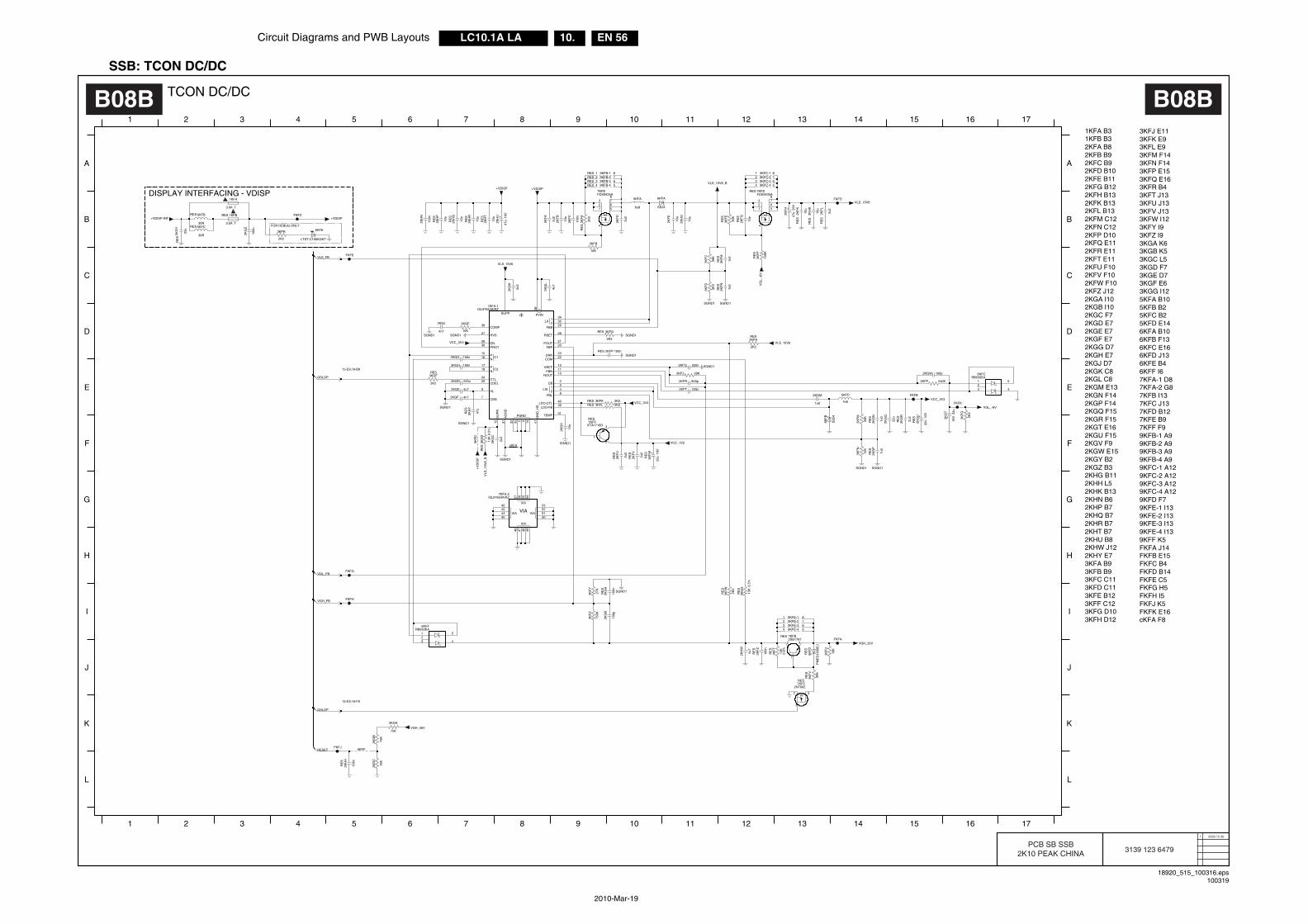
EN 56LC10.1A LA 10.Circuit Diagrams and PWB Layouts
2010-Mar-19
SSB: TCON DC/DC
18920_515_100316.eps100319
TCON DC/DCB08B B08B
2009-12-301
3139 123 6479PCB SB SSB
2K10 PEAK CHINA
2KFW F102KFZ J12
2KGU F152KGV F92KGW E152KGY B22KGZ B3
1KFB B3
2KFN C12
2KFA B82KFB B9
3KFF C123KFG D103KFH D12
3KFJ E113KFK E9
2KGA I10
1KFA B3
2KGT E16
5KFA B105KFB B25KFC B25KFD E146KFA B10
2KHG B11
2KFC B92KFD B102KFE B112KFG B122KFH B132KFK B132KFL B132KFM C12
2KFP D102KFQ E112KFR E112KFT E112KFU F102KFV F10
9KFC-1 A129KFC-2 A129KFC-3 A12
3KFL E9
2KGK C82KGL C82KGM E132KGN F142KGP F142KGQ F152KGR F15
3KGF E63KGG I12
FKFG H5FKFH I5FKFJ K5FKFK E16cKFA F8
6KFB F13
2KHW J122KHY E73KFA B93KFB B93KFC C113KFD C113KFE B12
9KFC-4 A129KFD F79KFE-1 I139KFE-2 I139KFE-3 I139KFE-4 I13
2KGB I102KGC F72KGD E72KGE E72KGF E72KGG D72KGH E72KGJ D7
3KFW I123KFY I93KFZ I93KGA K63KGB K53KGC L53KGD F7
FKFB E15FKFC B4FKFD B14FKFE C5
6KFC E166KFD J136KFE B46KFF I6
2KHH L52KHK B132KHN B62KHP B72KHQ B72KHR B72KHT B72KHU B8
7KFF F99KFB-1 A99KFB-2 A99KFB-3 A99KFB-4 A9
7KFA-1 D87KFA-2 G87KFB I137KFC J137KFD B127KFE B9
3KFM F143KFN F143KFP E153KFQ E163KFR B43KFT J133KFU J133KFV J13
3KGE D7
9KFF K5FKFA J14
VIA VIA
VIA
VIA
DRNCOM
VREFFBN
NOUT
CB12
FBL
LDO-CTLLDO-FB
TEMP
FBP
C1
PN
C2
LX
LXL
PGND
PVINSUPP
SU
PN
AG
ND
GN
D_H
S
COMP
HVS
ENPROT
PN
CTLCDEL
VL
CM2
12
FBB
RSET
POUT
11 12
1 15 16
E
C
D
E
1 2
17
A
B
C
D
13 14 15 16 17
10
DISPLAY INTERFACING - VDISP
FOR DEBUG ONLY
F
G
H
I
J
K
L
B
3 4 5 6 7 8 9 10
2 3 4 5 6 7 8 9 11 12 13 14
F
G
H
I
J
K
L
A
13K
3KG
DR
ES
0.5%
2KG
C
2u2
VLS
_15V
6_B
2KGH 100n
SGND1
SGND1 SGND1
1KFA
T3.0A
RES
T3.0A
1KFB
RES 5KFC
FKFJ
30R
+VDISP-INT
8
4
123
RE
S
100K
3KF
F
7KFDFDS9435A
567
9KFC-44 5
RES
SGND1
3K3
3KF
D
39K
3KF
C
2
3
RE
S2K
FU
2u2
KTA1718D7KFF
1
RES
RES
FKFG
3KGF
2K2
FKFE
9KF
D
2KH
U
47u
16V
4 5
10K
3KFB
3 69KFB-4RES9KFB-3RES
20K
3KF
M
SS
24
6KF
B
2KGM
1u0VCC_3V3
16V 2K
2
3KF
Q
2KG
T 22u
240K3KFP
2KH
P
10u
RE
S
10u
2KH
KR
ES
FKFC
9KFE-44 5
2KG
B
100p
4445
46 47 48 49
50
42
515253
54555657
43
ISL97653AIRZ7KFA-2
VIA
16K
3KG
C
2KG
Y
22u
RE
S
2KG
Z
100n
LTST-C190KGKT
+VDISP
6KFE
2K2
3KFR
SGND1 2K2
3KF
WR
ES
750K
3KF
Z
27K
3KF
Y
10u
2KH
G
2KG
K
2u2
RES 5KFB
30R
VG
L_-6
V
2KGF 4n7
47u
2KH
YR
ES
+V
DIS
P
VCC_3V336
38 1
28
12
31
9
10
3435
34
13
32 33 5 6 14
21
23
26
29
8
11
20
41
27
4039
37
1615
1817
225
7
22
30
24
7KFA-1ISL97653AIRZ
Φ
3
+VDISP
7KFB
1
2
RE
S
RES2SB1767
2KH
W
4u7
2KF
Z
100n
VLS_15V6
2KFP 100n
RES
RES
3KFH
2K2
FKFK
cKFA
2KF
H
47u
25V
FKFD
9KFC-33 6
2KF
W
22u
16V
2KF
VR
ES
RE
S2u
2
2KGD 220n
2KGE 4u7
2KF
E
10u
SS34
6KFA
6u8
5KFA
2u2
9KFC-11 8
2KF
D
2KH
N
100n
2KG
L
4u7
VLS_15V6
2KG
V
10n
VGL_-6V
SGND1
RE
S
1n0
2KF
N2K
FM
1n0
RE
S
RE
S
SGND1
2KH
T
10u
1 8
RE
S
10u
2KH
R
9KFB-1RES
5KFD
4u5
VGH_35V
2KH
H
100n
9KFF
RE
S
3KF
V
VGH_35V
RE
S
3K6
3KG
B
75K
9KFE-22 7
1
3
5
42
RB550EA6KFF
3KFL 2K2RES2K23KFK VCC_3V3RES
2KF
B
10u
+VDISP
2KF
A
2u2
5678
4
123
7KFEFDS9435A
2K2
3KF
AR
ES
100n
0.5%
13K
2KF
C
3KG
GR
ES
RE
S2K
GR
2u2
RE
S
2KG
Q
22u
1n0
2KG
N
2KF
L
2u2
VLS_15V6
RE
S
RE
S
15-E9,16-F9
15-E9,16-B9
2KF
K
10u
VCC_1V2
2KGG 100n
2KGJ
4n7 10K
3KGE
2KGW 100p
1
3
5
42
SGND1
RB550EA6KFC
FKFH
2 7
39K3KFJ
SGND1
9KFC-2
2KF
G
10n
RE
S
39K
3KF
ER
ES
SGND1
VLS_15V6_B
3KF
N
SGND1
12K
75K
3KGA
1
2
FKFA
RES
2N70027KFC
3
3KF
U
10K
PM
EG
1030
EJ
6KF
D
9KFB-2RES 2 7
RE
S
FKFB
SGND1
9KFE-33 6
RE
S2K
GA
100n
2KFT 220n
2KFR 820p
RE
S2K
GP
1n0
RES
2K2
3KFG
2KG
U
22u
16V
RE
S
1 8
RE
S3K
FT
0.5%
13K
SGND1
9KFE-1
10u
2KH
Q
SGND1
RE
S
2KFQ 220n
RESET
VGH_FB
GSLOP
GSLOP
VLS_FB
VGL_FB
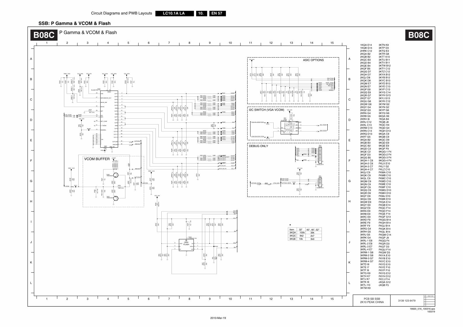
Circuit Diagrams and PWB Layouts EN 57LC10.1A LA 10.
2010-Mar-19
SSB: P Gamma & VCOM & Flash
18920_516_100316.eps100319
P Gamma & VCOM & FlashB08C B08C
2009-12-301
3139 123 6479PCB SB SSB
2K10 PEAK CHINA
1KQA E141KQB G142HRK C122KQA B22KQB B22KQC B32KQD B42KQE B4
2KQK D82KQM E72KQN E72KQP E82KQQ E82KQR G7
2KQF B52KQG D72KQH D72KQJ D8
2KQT G72KQU G82KQW G82KQY G4
2KRA G42KRB G52KRH I82KRJ C122KRL C132KRM C132KRN C142KRQ D132KRT G5
3KQB B33KQC B23KQD C33KQE C23KQF D33KQG B53KQH-1 C83KQH-2 C83KQH-3 C73KQH-4 C73KQJ C93KQK C9
3KQM C93KQN C93KQP C93KQQ C93KQR D93KQT D93KQU D93KQW E93KQY E9
3KRA E93KRB E93KRC E93KRD F93KRE F93KRF F93KRG G43KRH G53KRJ G53KRK G43KRL-1 E83KRL-2 E8
2KQZ G3
3KRL-4 E73KRM-1 G83KRM-2 G83KRM-3 G73KRM-4 G73KTD I63KTE I73KTF I93KTG K9
3KQA B2
3KTJ K73KTK I93KTL I103KTM K9
3KTN K93KTP D33KTQ E33KTR G83KTT K103KTU B113KTV B11
3KQL C9
3KTY C123KTZ C123KYA B123KYB B123KYC B133KYD B133KYE C133KYF C133KYG C14
3KQZ E9
3KYJ G133KYK C123KYM G23KYN G23KYP G63KYQ G6
3KRL-3 E7
6KQA H67KQA B47KQB J87KQC H47KQD G47KQH D139KQA C99KQB C9
3KTH K7
9KQD E99KQE E99KQF F99KQG-1 F49KQG-2 F49KQG-3 F4
FKYC E10
9KQG-4 F4FKLX E10
3KTW B12
FKLZ C10FKMA C10FKMB C10FKMC C10FKMD C10FKME C10FKMF C10FKMG D10FKMH D10
3KYH G13
cKQA G12cKQB F5
FKMJ D10FKMK E10FKQA E14FKQB E14FKQC F14FKQD F14FKQE F14FKQF G13FKQG B14FKQH B14FKQJ B14FKQK B14FKQL B14FKQM C14FKQP J9FKQQ F4FKQR D3FKQT D3FKQU F14FKQW D3FKYA E10FKYB E10
9KQC D9
FKYD E10FKYE F10FKYF F10FKYG E12FKYH D12FKYJ F14
FKLY G2
INPCOM|DVR_OUT
REFIN_INN
REFIN
SET
SCLSDA
SET_COMP
V_THERM
BANKSEL
GND_HS
VIA
GND
OUT10
OUT11
OUT12
OUTCOM
INNCOM
AVDDOUT1
OUT2
OUT3
OUT4
OUT5
INN5
OUT6
INN6
OUT7
INN7
OUT8
INN8
OUT9
VSD
-BUSCTRLFIL
I 2 CINP
SI
SO
CS
HOLD
WP
SCK
5 6 7
VCOM BUFFER
NC
Item
G
H
I
8
K
L
3KQC 6k2 2k73KQE 10k 3k9
*
*
1 2 3 4 9 10 11 12 13 14 15
2 3 4 5 6 7
NC
32"
*
40", 46", 52"
9 10 11 12 13 14 15
A
J
C
D
E
F
G
H
I
J
K
A
B
C
D
E
F
ASIC OPTIONS
8
1
*
3KQA 100k 39k
B
L
NC
NC
DEBUG ONLY
I2C SWITCH (VGA VCOM)
NC
FKYA
RES 3KRB 100R
RES
RE
S
100R3KQP
RES
3KY
B
2K0
100R3KQM
9KQARES 3KQK 100R
100R3KQLRES
3KQJ 100RRES
FKQR
2KQ
N
RE
S
100n
2K2
3KT
G
100R3KRARES
2K2
3KY
K
7KQDPBSS4540X
RE
S3K
TZ
2K2
0K2
3KY
A
3KT
U
2K2
2K2
3KT
V
FKQT
RE
S3K
TH
2K2
16V
22u2K
QZ
FKMKFKLX
100K
0.5%
3KQ
A
FKMC
3KQN 100R
FKMG
FKMFRES FKME
FKMD
FKQH
RE
S10
0n
2KR
T
RE
S10
K
3KY
P
2KQ
M
100n
FKYCFKYB
3KQ
E
10K
0.5%
3KQZ 100R
FKQP
RES
3KY
Q
10K
RE
S
0.5%
3KQ
C
6K2
3KQ
B
22K
0.5%
VREF_15V2 VLS_15V6
VREF_15V2
9KQE
1u0
2KQ
A
1u0
2KQ
B
10R
27
3KR
L-2
FKMH
FKMJ
2KQ
J
100n
27
VREF_15V2
3KQ
H-2
10R
10R
3KQ
H-3
36
3KQ
H-4
10R
45
100n
2KQ
K
VLS_15V6VLS_15V6
2KQ
E
100n
3KQ
D
18K
0.5%
100R3KRDRES
3KRF 100R
RE
S
RES
RE
S10
K
3KY
N3K
YM
10K
FKQG
100R3KRCRES
2KQ
P
100n
18
29
31
10R
3KR
L-1
28
30
3435363738394041
10
16
18
19
25
32
1
1312
26
27
2
22
23
24
3
4
7
8
5 21
14
6 20 33
9
11
15
17
ISL24837IRZ-T137KQA
10R
3KQ
H-1
18
2KQ
W
100n
FKQJ
1n0
2KR
N
RE
S
RE
S
2KR
M
1n0
1n0
2KR
L
3KRERES
RE
S
100R
1n0
2KR
J
9KQF
RE
S
RE
S
10K
3KY
H
+VDISP
2KQ
G
100n
2KQ
H
100n
9KQB
RES 3KQQ 100R
PBSS5330X7KQC
45
36
9KQ
G-4
9KQ
G-2
27
9KQ
G-3
4u7
2KR
H
10V
2K2
WT
K3Y
TK3
2K0
RE
S
2K2
3KT
JR
ES
FKQU
FKMB
FKLZ
FKMA
FKLY
100n
2KQ
D
3KQ
G
2K2
0.5%
2K0
3KY
CR
ES
FKQD
FKQBFKQC
RE
S
VCC_3V3
2HR
K
1n0
3KY
J
10K
VCC_3V3
RE
S
10R
3KR
L-3
36
2KQ
T
100n
100n
2KQ
R
18
100n
2KQ
U
3KR
M-1
10R
10R
3KR
M-2
27
3KR
M-3
10R
36
45
FKQL
10R
3KR
M-4
FKQK
FKQW
100n
2KR
Q
SD0
7SD12 SDA
3
VDD
6VSS
RE
S
7KQHPCA9540B
5SC0
8SC1
4LCS1
RES
3KT
E
2K2
FKQF
RE
S
FKQE
VLS_15V6
9KQD
10u
2KQ
F
RES 100R3KQTRES 3KQR 100R
9KQC
10K
3KT
Q
10K
RE
S3K
TP
RE
S3K
TK
2K2
cKQA
1234
56
RES1KQB
502382-0470
FKQA
FKYH
3456789
1011
1KQA
502382-0970
12
RES
2
8
3
3KT
M
2K2
AT25DF321-SU7KQB
FLASH
Φ(32K) 1
4
7
6
5
45
3KR
L-4
10R
100n
2KQ
Q
3KR
G
0R51
100n
2KQ
C
0.5%
3KQF
3K3
2K2
RE
S3K
TT
FKQM
VCC_3V3
3KY
G
2K2
2K2
3KY
F
3KT
R
2K2
VCC_3V3
3KY
D
2K0
RE
S
2K2
FKQQ
3KY
E
3KQY 100RRESRES
FKYD
100R3KQW
3KQ
U
2K2
RE
S
4K7
3KT
F
2K2
3KT
LR
ES
MS
S1P
4
VCC_3V3
6KQ
A
FKYG
2K2
3KT
D
RE
S3K
TN
2K2
3KRJ
750R 0.5%
FKYJ
1K0
0.5%
RE
S
3KR
H
100n
2KR
A
10u
2KQ
Y
68p
2KR
B
VCC_3V3
cKQ
B
9KQ
G-1
18
0R51
3KR
K
19-C10,19-C7
19-C10,19-C7
19-C10,19-C717-F7,19-C10,19-C719-C10,19-C7
17-D5
FKYF
6-D3
18-D13,18-J19
17-E9
FKYE
17-D9
18-F2,18-J19
17-D4VCOM
OUTCOM
OUTCOM
SDOSCSSDIWPVCC
EN
SDA-TCONSCL-TCON
BYPASS_MODEBYPASS_MODE CTRL-DISP
SCK
EN
SCS
VGA-SDA-EDID-TCON
SDA-TCON
SCL-TCON
VGA-SCL-EDID-TCON
WP
VCC
SCKSDO
SDI
MODE2
SELLVDSR_LU_D
SCL-TCON
100HZ_120HZ
SDA-TCON
OS_ON-OFF
VL191VL159VL127
INNCOM
VH95
VH159VH191
VH127
VH63VH95
VL95
VL63VL95
VL159VL127
VL31
SDA-TCON
VH127VH159VH191VH247
VH63
VH31
VL63
VL247
VL191
VH0
VL0
INNCOM
VH255
VL255
CS_H
CS_L
OUTCOM
SCL-TCON
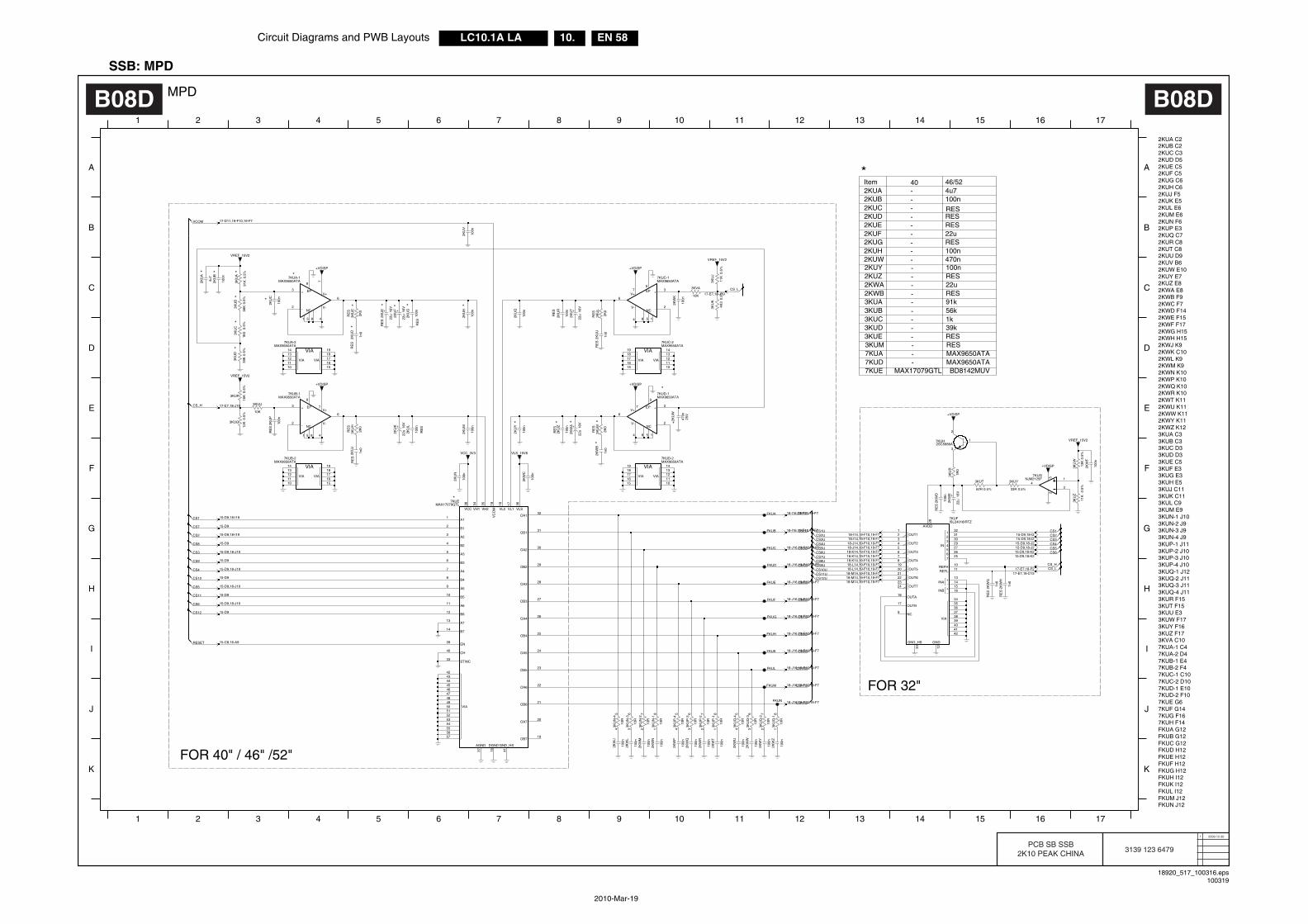
EN 58LC10.1A LA 10.Circuit Diagrams and PWB Layouts
2010-Mar-19
SSB: MPD
18920_517_100316.eps100319
MPDB08D B08D
2009-12-301
3139 123 6479PCB SB SSB
2K10 PEAK CHINA
2KWC F72KWD F142KWE F152KWF F172KWG H15
FKUH I12
FKUD H12FKUE H12
2KWB F9
FKUK I12
FKUM J12FKUN J12
2KWA E8
2KWH H152KWJ K9
FKUF H12FKUG H12
3KUB C3
3KUD D3
7KUG F167KUH F14FKUA G12FKUB G12FKUC G12
3KUM E9
3KUP-3 J103KUP-4 J10
FKUL I12
2KUF C52KUG C6
7KUB-1 E4
7KUC-1 C10
2KUY E72KUZ E8
2KWK C102KWL K9
2KWN K10
2KWQ K102KWR K102KWT K112KWU K112KWW K112KWY K112KWZ K123KUA C3
3KUC D3
3KUK C113KUL C9
3KUQ-1 J123KUQ-2 J11
3KUQ-4 J11
3KUT F153KUU E33KUW F173KUY F163KUZ F173KVA C107KUA-1 C47KUA-2 D4
7KUB-2 F4
2KUR C82KUT C82KUU D92KUV B62KUW E10
2KUJ F5
2KWM K9
3KUE C53KUF E33KUG E33KUH E53KUJ C11
3KUQ-3 J11
7KUC-2 D107KUD-1 E107KUD-2 F107KUE G6
2KUQ C7
2KUH C6
2KUK E52KUL E62KUM E62KUN F6
2KWP K10
7KUF G14
3KUR F15
3KUP-2 J10
2KUB C22KUC C32KUD D52KUE C5
2KUP E3
2KUA C2
3KUN-1 J103KUN-2 J93KUN-3 J93KUN-4 J93KUP-1 J11OUT2
OUT3
OUT4
OUT5
OUT6
OUT7
+
REFLREFH
7654321
AVDD
VIA
-
GND_HS GND
NC
OUTB
OUTA-
INA
+INB
IN
OUT1
VIA VIA
EP
NC
V+
-
+
V-
EP
NC
V+
-
+
V-
VIAVIA
EP
NC
V+
-
+
V-
VIAVIA
EP
NC
V+
-
+
V-
VIA VIA
VH1 VH2
VC
OM VL2 VL1 VLS
OA3
OB3
OA4
OB4
OA5
OB5
OA6
OB6
OA7
OB7
VIA
GND_HSDGNDAGND
A1
B1
A2
B2
A3
B3
A4
B4
A5
B5
A6
B6
A7
B7
EN
CH
ST|NC
VCC
OA1
OB1
OA2
OB2
16
RES
4 5
-
2KWB
2KUD
I
14
2KUF
- 22u
16 17
A
22u2KUG - RES2KUH - 100n2KUW -
2KWA
2KUY - 100n2KUZ - RES
12 13
6 7
17
9
15
1 2 3
2KUC
12 13 15
470n
7 8 9 10 11
8
100n
14
-
FOR 40" / 46" /52"
FOR 32"
MAX9650ATA
Item
*
I
J
K
*
61 2 3 4 5
J
K
A
C
D
11
- RES7KUA -
2KUE
7KUD - MAX9650ATA7KUE MAX17079GTL BD8142MUV
*
B
D
F
G
H
E
F
G
H
* * * *
*
*
*
*
402KUA - 4u72KUB
-3KUA - 91k
1k
10
RES
- RES
3KUB - 56k3KUC -*
*
*
- RES
46/52
*
C
*
E
* *
*
* *
*
*
3KUD - 39k3KUE - RES3KUM
-
B
FKUG
FKUH
FKUF
FKUE
FKUD
FKUK
VLS_15V6
100n
2KW
C
100n
VCC_3V32K
UN
RE
S
2K0
3KU
M
36
10R
3KU
P-3
100n
2KW
Z
2KW
Y
100n
100n
2KW
W
10R
3KU
N-4
45
FKUN
100n
2KW
R
100n
2KW
P
3KU
Q-3
10R
36
FKUM
100n
36373839404142
2KW
T
21222324
18
17
1011
3435
9
123456781920
313029272625
13141516
7KUFISL24016IRTZ28
1233
32
2KW
Q
100n
RE
S
1n0
2KU
J
1n0
2KW
HR
ES
2KW
G
1n0
RE
S
FKUC
FKUB
FKUA
FKUL
27
18
10R
3KU
Q-2
10R
3KU
P-1
2KU
A
4u7
3KU
Q-1
10R
18
100n
2KW
N
2KW
M
100n
100n
2KW
L
2KW
J
100n
3KU
N-1
10R
18
+VDISP
33R 0.5%
3KUY
0.5%62R
3KUT
1R0
3KU
R 2KW
F
100n
10K
3KUU
6
7
4
+VDISP
7KUB-1MAX9650ATA
9
3
2
1 5 8
RE
S3K
UH
3KU
P-2
10R
27
2K0
45
3KU
P-4
10R
16V
22u2K
UK
2KU
F
22u
16V
2KU
H
100n
3KU
N-3
10R
36
2KW
E10
0n
22u
16V
RE
S2K
WD
1314
15161718
7KUA-2MAX9650ATA
VIA
10
19
1112
45
2KU
B
100n
10R
3KU
Q-4
VREF_15V2
2KW
U
100n
3KUF
0.5%
12K3KUG
0.5%
%5.0K61
39K3K
UD
1K03K
UC
VREF_15V2
0.5%
27
3KU
B
56K
0.5%
10R
3KU
N-2
100n
2KU
P2K
UC
100n
RE
S
+VDISP
100n
2KU
V
10
19
11121314
15161718
VIAMAX9650ATA
7KUB-2
3
2
1 5 8
6
74
MAX9650ATA7KUA-1
9
0.5%
3KU
K
4K3
VREF_15V2
2K0
3KU
ER
ES
RE
S2K
UD
1n0
22u2K
UE
14
15161718
RE
S
16V
7KUD-2MAX9650ATA
VIA
10
19
111213
4
+VDISP
9
3
2
158
6
7
MAX9650ATA7KUD-1
19
11121314
15161718
VIAMAX9650ATA7KUC-2
10
100n
2KU
M
2
158
6
7
4
+VDISP
7KUC-1MAX9650ATA
93
3KU
L
2K0
RE
SR
ES
1n0
2KU
U2K
WB
1n0
2KW
A
22u
16V
2KU
T
22u
16V
100n
2KU
Q2K
UY
100n
32SC5886A7KUH 1
2
47484950
1716 36
525354555657
43444546
25
23
21
19
33
38 1834 35
42
51
30
28
26
24
22
20
31
29
27
6
8
10
12
14
40
15
39
41
321
3
5
7
9
11
13
37
2
4
7KUEMAX17079GTL
0.5%
91K3K
UA
10K
18-J16,19-F10,19-F7
3KVA
100n
2KU
Z2K
UR
100n
RE
S
VREF_15V2
RE
S
2KU
L
100n
RE
S
11K
3KU
J
0.5%
100n
2KU
G
2KU
W
470n
25V
RE
S
100n
2KW
K
15-D9
13K
3KU
W
0.5%
18-I16,19-F10,19-F7
+VDISP
18-J16,19-F10,19-F7
18-L14,19-F10,19-F7
15-D9
18-J16,19-F10,19-F7
17-E7,18-D13
17-E7,18-J19
17-E7,18-F2
18-J16,19-F10,19-F7
18-L14,19-F10,19-F7
15-D9
15-D9,18-J19
15-D9,18-K2
17-E7,18-J19
18-J16,19-F10,19-F7
18-K14,19-F10,19-F7
15-D9,18-J19
15-D9,18-K2
18-J16,19-F10,19-F7
18-K14,19-F10,19-F7
52
17-D11,19-F10,19-F7
15-C8,16-A9
18-K14,19-F10,19-F7
15-D9
7KUGNJM2125F 1
34
15-D9,18-I19
15-D9,18-I2
18-J16,19-F10,19-F7
18-M14,19-F10,19-F7
18-J16,19-F10,19-F7
18-M14,19-F10,19-F715-D9
18-I16,19-F10,19-F7
18-I14,19-F10,19-F7
18-J16,19-F10,19-F7
18-M14,19-F10,19-F7
15-D9
0.5%
18-I14,19-F10,19-F715-D9,18-I19
15-D9,18-I2
11K
3KU
Z
15-D9,18-J218-J16,19-F10,19-F718-J14,19-F10,19-F7
15-D9,18-J19
15-D9,18-J2
CS_L
18-J14,19-F10,19-F7
15-D9,18-J19
CS_H
CS2
CS8
CS3
CS9
CS4
CS10
CS5
CS11
CS6
CS12
CS10U
CS12U
CS11U
RESET
VCOM
CS1
CS7
CS4UCS3UCS2UCS1U
CS6CS5CS4CS3CS2CS1
CS1U
CS2U
CS3U
CS4U
CS5U
CS6U
CS7U
CS8U
CS9U
CS_LCS_H
CS12UCS11UCS10UCS9UCS8UCS7UCS6UCS5U
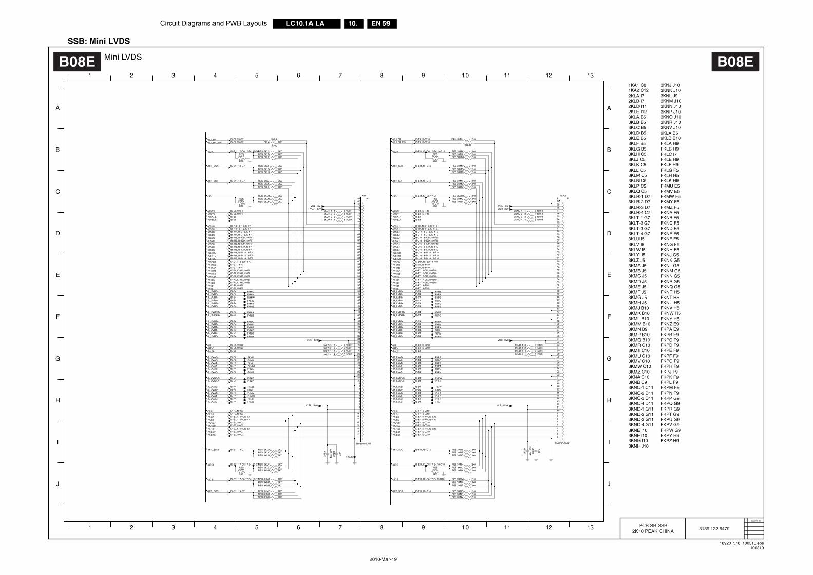
Circuit Diagrams and PWB Layouts EN 59LC10.1A LA 10.
2010-Mar-19
SSB: Mini LVDS
18920_518_100316.eps100319
Mini LVDSB08E B08E
2009-12-301
3139 123 6479PCB SB SSB
2K10 PEAK CHINA
9KLB B10FKLA H9FKLB H9FKLC I7FKLE H9FKLF H9
3KMK B103KML B10
2KLA I7
3KMR C103KMT C103KMU C10
3KMH J53KMJ B10
FKPA E9FKPB F9
3KNK J103KNL J9
3KNH J10
3KNJ J10
FKNJ G5FKNK G5
3KLT-1 G73KLT-2 G7
3KNM J103KNN J10
3KLT-3 G73KLT-4 G7
FKNV H5FKNW H5FKNY H5FKNZ E9
3KLR-1 D73KLR-2 D73KLR-3 D73KLR-4 C7
FKNE F5FKNF F5
FKPC F9FKPD F9
3KNP J103KNQ J10
3KMM B103KMN B9
3KNR J103KNV J109KLA B5
FKNA F5FKNB F5FKNC F5FKND F5
2KLB I72KLD I11
3KMV C103KMW C10
FKNG F5FKNH F5
FKNL G5FKNM G5
3KMP B103KMQ B10
FKNQ G5FKNR H5FKNT H5FKNU H5
3KND-4 G113KNE I103KNF I103KNG I10
FKPY H9FKPZ H9
1KA1 C81KA2 C12
FKPE F9FKPF F9
FKLG F5FKLH H5
FKMV E5FKMW F5FKMY F5FKMZ F5
3KMD J53KME J53KMF J53KMG J5
FKPG F9FKPH F9
FKPL F9FKPM F9
2KLE I123KLA B5
3KMZ C103KNA C103KNB C93KNC-1 C11
FKNN G5FKNP G5
3KNC-4 D113KND-1 G113KND-2 G113KND-3 G11
3KLM C53KLN C53KLP C53KLQ C5
FKPV G9FKPW G9
FKLK H9FKMU E5
3KLZ J53KMA J53KMB J53KMC J5
FKPT G9FKPU G9
FKPJ F9FKPK F9
FKPN F9FKPP G9
3KLB B53KLC B5
3KNC-2 D113KNC-3 D11
3KLH C53KLJ C53KLK C53KLL C5
3KLU I53KLV I53KLW I53KLY J5
FKPQ G9FKPR G9
3KLD B53KLE B53KLF B53KLG B5
J
A
10 11 12
F
G
H
I
4 5 6 7 8 9
I
J
2 3
7 8
C
D
B
C
D
E
5 6 9 10 11 12
13
E
F
A
13
B
1 2
1
G
H
3 4
3KND-3 100R3 6
VCC_3V3
VGH_35V
VCC_3V3
FKLAFKLBFKLEFKLF
2K03KMERES
FKPD
2K03KMCRES
FKNT
FKNVFKNW
RES 2K03KLW
3KLURES
FKLH
100R4 5
2K0
RES
3KLT-4
3KLA 2K0
VGL_-6V
9KLA
VGH_35V
RES 3KMR 2K02K03KMQRES
FKNN
FKPG
FKNU
FKLC
3KLR-2 2 7
4 5
100R
100R3KLR-4
RES 3KMV 2K02K03KMURES
3KMT 2K0
25V
RES
2KLA
47u
RES 3KMZ 2K0
FKPVFKPU
RES
FKPZ
FKPP
2K03KNH
3KNKRES
FKPT
3KNJ 2K02K0
RES
RES 3KMD 2K0
3KMB 2K0RESRES
2K03KLZRES 3KLY 2K0
3KLV 2K0
8
RES
3KLT-1 100R13KLT-2 100R2 73KLT-3 100R3 6
FKPF
FKPY
FKPAFKNZ
FKPBFKPC
3KNARES 2K0
2K03KMWRES
FKNL
FKNJ
FKNM
FKNR
RES
FKNP
2K03KNF
8
RES 3KNE 2K0
3KND-1 100R1
3 6 100R3KLR-3
25V
47u2K
LD
FKNA
22n
2KLB 22
n
2KLE
FKNY
RES
FKPW
2K0
3KNB
FKPM
FKPR
RES
FKLK
2K03KNQ
FKPQ
RES3KMA
2K0
RES 3KMH 2K02K03KMGRES
3KMF 2K0RES
2K0
3KNLRES
FKNB
FKNE
FKNHFKNG
FKNK
FKMYFKMZ
RES 3KLG 2K0
3KNG 2K0
3KLE 2K0
RES
RESRES
2K03KLD
1 8
RES 3KLC 2K0
100R3KLR-1
RES 3KMP 2K0
3KMN
2K0
RES0K2SER
2K03KMMRES 3KML
FKPH
FKPE
FKPKFKPL
FKPN
81 82
73747576777879
8
80
9
646566676869
7
707172
53545556575859
6
60616263
444546474849
5
505152
3536373839
4
40414243
2526272829
3
3031323334
1516171819
2
2021222324
1KA2
196250-80041
1
1011121314
3KLQ
2K0
RES
RES 2K03KNV
FKMV
FKNF
FKLG
FKMU
FKMW
3KLM 2K0
RES
RES
2K03KLH
2K03KLFRES
3KMKRES
FKPJ
2K0
3KNC-3 100R3 6
FKNQ
FKNDFKNC
9
81 82
7273747576777879
8
80
63646566676869
7
7071
53545556575859
6
606162
444546474849
5
505152
33343536373839
4
40414243
242526272829
3
303132
141516171819
2
20212223
1
10111213
196250-80041
1KA1
RES
2K0
3KLB
RES 3KNR 2K0
RES 3KLK 2K0
3KNP 2K0RESRES
2K02K03KNN
RES 3KNM
100R4 5
7
3KNC-4
3KNC-2 100R23KNC-1 100R1 8
VLS_15V6
17-E7,17-F7,19-C717-E7,19-C10
17-E7,19-C717-E7,17-F7,19-C10
3KLLRES
RES
2K0
2K03KLJ
RES 3KLP 2K02K03KLNRES
15-E11,17-C6,17-E4,19-G7
15-E11,17-B6,17-E4,19-B1015-E11,17-B6,17-E4,19-B7
15-E11,17-C6,17-E4,19-G10
2 7
VLS_15V6
100R3KND-2
17-E7,19-C7
17-F7,19-C1017-F7,19-C7
17-F7,17-G7,19-E10
15-E9,19-D7
15-E415-E4
17-E7,19-C717-E7,19-C10
17-F7,19-C7
17-E7,19-C1017-E7,19-C717-E7,19-C10
15-E9,19-D10
15-D415-D4
15-C415-C4
15-E9,19-G715-E9,19-G1015-E9,19-G7
15-C415-C4
17-D11,18-B2,19-F7
15-E11,17-C6,17-E4,19-C1015-E11,17-C6,17-E4,19-C7
15-E11,17-B6,17-E4
15-E9,19-G10
100R3KND-4 4 5
RES
9KLB
2K03KMJ
VGL_-6V
15-E4
17-F7,17-G7,19-E717-F7,17-G7,19-E1017-F7,17-G7,19-E717-F7,19-E10
15-E415-E4
15-E415-E4
15-E4
15-E4
18-J16,18-M14,19-F1018-J16,18-M14,19-F718-J16,18-M14,19-F1018-J16,18-M14,19-F7
17-E7,17-F7,19-C1017-E7,17-F7,19-C717-F7,19-C10
15-D415-D4
15-D4
15-C4
17-E7,17-F7,19-C7
15-E915-E9
15-C415-C4
15-C4
15-E9,19-F1015-E9,19-F715-E9,19-F1015-E9,19-F7
15-F4
15-E915-E9
15-E11,19-G1015-E11,19-G7
17-F7,17-G7,19-E7
17-F7,19-E1017-F7,19-E7
17-D11,18-B2,19-F10
15-F4
17-G7,19-F1017-G7,19-F717-G7,19-F10
18-J16,18-K14,19-F7
15-E415-E4
15-E415-E4
17-F7,19-E7
18-J16,18-K14,19-F1018-J16,18-K14,19-F718-J16,18-K14,19-F1018-J16,18-K14,19-F718-J16,18-K14,19-F10
18-I14,18-I16,19-F7
18-J16,18-L14,19-F1018-J16,18-L14,19-F718-J16,18-L14,19-F1018-J16,18-L14,19-F7
15-D4
15-D415-D4
18-I14,18-I16,19-F1018-I14,18-I16,19-F718-I14,18-I16,19-F10
15-D4
17-E7,17-F7,19-C10
15-D4
18-J16,18-M14,19-F7
15-E11,19-C1015-E11,19-C7
15-C415-C4
15-D4
15-F415-F4
15-F415-F4
18-J16,18-M14,19-F10
15-E4
15-E415-E4
15-F415-F4
15-F4
15-E11,19-G1015-E11,19-G7
15-E11,19-B1015-E11,19-B7
15-E4
17-F7,17-G7,19-E717-F7,17-G7,19-E10
15-F415-F4
15-F4
15-E9,19-D7
17-G7,19-F717-F7,17-G7,19-E1017-F7,17-G7,19-E717-F7,17-G7,19-E10
18-J14,18-J16,19-F718-J14,18-J16,19-F1018-J14,18-J16,19-F7
15-E915-E9
15-E9,19-D10
15-D415-D4
15-D415-D4
18-J14,18-J16,19-F10
BIT_SDO
SDO
SCS
BIT_SCS
15-D415-D4
BIT_SDO
SDO
SCS
BIT_SCS
SCK
BIT_SCK
SDI
BIT_SDI
LS_L
FSREV
G_LBRG_LBR_INV
LS_R
FSREV
SCK
BIT_SCK
SDI
BIT_SDI
GCK_RGSP1GSP2
VL63VL31
G_LBRG_LBR_INV
VCOMCS12UCS11UCS10UCS9UCS8UCS7UCS6UCS5UCS4U
VL95
CS3UCS2UCS1U
GOE_R
R_LVB5-
VL159
R_LVB5+VH0VH31VH63VH95VH127VH159VH191VH247VH255
VL127
VL191
R_LVB2+
R_LVCKB-R_LVCKB+
R_LVB3-R_LVB3+R_LVB4-R_LVB4+
R_LVA5-R_LVA5+
VL247
R_LVB0-R_LVB0+R_LVB1-R_LVB1+R_LVB2-
R_LVA3-R_LVA3+R_LVA4-R_LVA4+
R_LVA1-R_LVA1+R_LVA2-R_LVA2+
VL255
R_LVCKA-R_LVCKA+
VL31VL0
R_LVA0-R_LVA0+
CS10UCS9UCS8UCS7UCS6UCS5UCS4U
VL95
CS3UCS2UCS1U
GOE_LGCK_LGSP1GSP2
VL63
VH127VH159VH191VH247VH255
VL127
VCOMCS12UCS11U
L_LVB3+L_LVB4-L_LVB4+L_LVB5-
VL159
L_LVB5+VH0VH31VH63VH95
L_LVB1-L_LVB1+L_LVB2-
VL191
L_LVB2+
L_LVCKB-L_LVCKB+
L_LVB3-
L_LVA5-L_LVA5+
VL247
L_LVB0-L_LVB0+
L_LVCKA+
L_LVA3-L_LVA3+L_LVA4-L_LVA4+
L_LVA1-L_LVA1+L_LVA2-L_LVA2+
VL255
L_LVCKA-
VL0
L_LVA0-L_LVA0+

EN 60LC10.1A LA 10.Circuit Diagrams and PWB Layouts
2010-Mar-19
Layout Small Signal Board (Top Side)
1211
1212
1328
1735
1D04
1E01
1E02
1E05
1E06
1E07
1E08
1E09
1E10
1J04
1KA11KA2
1KAA
1KFA
1KFB
1KQA
1KQ
B
1L01
1M20
1M95
1M99
1P021P03
1P05
1P08
1T01
2101
2107
21112149
2150
2151
2152
2153
2154
2155
2159
2165
2177
2180
2226
2227
2228 22
29
2300
2301
2302
2303
2304
2306 2307
2308 2309
2312
2314
2316
2317
23182319
2330
2331
2332
2334
2335
2337
2338
2A00
2A012A02
2A03
2A04
2A06
2A20
2A21
2A24
2A25
2A262A27
2A292A30
2A31
2A32
2A33
2A34
2A35
2A36
2A37
2A38
2A39
2A40
2A412A42
2A43
2A44
2A452A46
2A47
2A48 2A49
2A50
2A51
2A52
2A53
2A55
2A56
2B00
2B01
2B02
2B032B05
2B07
2B08
2B092B10
2C09
2C12
2C15
2C282C29
2D00
2D01
2D02
2E00
2E01
2E02
2F00
2F01
2F02
2F03
2F04
2F05
2F06
2F07
2F09
2F10
2F11
2F12
2F13
2F14
2F19
2F20
2F22
2G062G09
2G10
2G11
2G12
2G21
2G24
2G252G26
2G27
2G52
2G53
2H04
2H05
2H06
2H07
2H08
2H09
2H10
2H11
2H12
2H17
2H18
2H19
2HRK
2J01
2J50
2J51
2J52
2KC
E
2KC
F
2KC
G
2KC
H
2KCJ
2KC
K
2KC
L
2KD
C2K
DD
2KFA
2KF
B
2KF
C
2KFD
2KF
E
2KF
H
2KF
M
2KF
N
2KF
P
2KFT
2KGC
2KG
D
2KGG
2KGH
2KG
J
2KGK
2KG
L
2KG
M
2KG
N2K
GP
2KG
Q
2KG
R
2KG
U
2KG
V
2KG
Y
2KG
Z
2KH
G
2KH
N
2KH
P
2KH
Q
2KH
R
2KH
T
2KHU
2KLA2KLB
2KLD
2KLE
2KQ
A
2KQ
B
2KQ
C
2KQ
F
2KQG
2KQH
2KQJ
2KQK
2KQ
M
2KQ
N
2KQ
P
2KQ
Q
2KQR
2KQT
2KQU
2KQW
2KQY
2KQZ
2KR
A
2KRB
2KRJ
2KRN2KR
Q
2KR
T
2KU
H
2KUJ
2KUK
2KUM
2KUP
2KWD
2KWE
2KWG2KWH
2KW
J
2KW
L
2KW
M
2KW
N
2KW
P
2KW
Q2K
WR
2KW
T
2KW
U2K
WW
2KW
Y
2KW
Z
2L00
3300
3303
3309
3C123C13
3C29
3C30
3C33
3C34
3C73
3C74
3C75
3C76
3D023D16
3D25
3D26
3D27
3E01
3E02
3E043E053E06
3E073E08
3E09
3E10
3E11
3E14
3E15
3E163E17
3E18
3E19
3E20
3E21
3E22
3E23
3E25
3E26
3E27
3E28
3E29
3E30
3E31
3E32
3E33
3E343E35
3E36
3E37
3E38
3E39
3E40
3E41
3E42
3E46
3F00
3F02
3F17
3F18
3F19
3F24
3F25
3F26
3F42
3F43
3F44
3F45
3F683F69
3G093G12
3G133G14
3G15
3G24
3G27
3G283G29
3G30
3G56
3G57
3H11
3H13
3H143H16
3H17
3H19
3H20
3H22
3H26
3H27
3H28
3H29
3H30
3H31
3H32
3H33
3H36
3K023K03
3K04
3K053K51
3K54
3KA
A
3KAB
3KAG3KAH
3KAJ3KAK
3KA
L
3KA
M
3KAN 3KAP
3KAQ3KAR
3KAT
3KAU
3KAV 3KAW
3KAY
3KAZ
3KBA
3KBB 3KBC
3KBD3KBE
3KBF
3KBG
3KB
U3K
BV
3KB
W3K
BY
3KBZ
3KC
A3K
CB
3KF
A
3KF
B
3KF
C3K
FD
3KF
G
3KF
H
3KF
M3K
FN
3KF
R
3KF
W
3KGD
3KG
E
3KG
F 3KLA
3KMJ3KNC
3KQA
3KQ
B
3KQC
3KQ
D
3KQE
3KQ
F
3KQG
3KQ
H
3KQJ3KQ
K
3KQM
3KQN
3KQP
3KQQ
3KQR
3KQT
3KQU
3KQZ
3KRA
3KRD
3KRE
3KRF
3KRG
3KRH
3KRJ
3KR
K
3KRL
3KR
M
3KTL
3KT
M
3KT
N
3KTT
3KTW3KTY
3KTZ
3KUF3KUG
3KUH
3KUN 3KUP
3KUQ
3KU
R 3KUT
3KUU
3KUY
3KYA
3KYD
3KYF
3KYG
3KYH
3KYJ
3KYM3KYN
3L00
3L01
3L02
4100
4300
4302
4303
4D05
4E00
4E01
4E02
4H04
4H05
5100
5101
5102
5104
5105
5106
5109
5206
5207
5300
5301
5302
5303
5A00
5A02
5A03
5A045A05
5A06
5A07
5A08
5A09
5A10
5A11
5A12
5D00
5H01
5H02
5H03
5J02
5J14
5KAG5KFA
5KF
B
5KF
C
5KF
D
5L00
5L01
5L02
6100
6101
6102
6103
6104
6C06
6C07
6C08
6D00
6E00 6E01
6E026F006F01
6G13
6G14
6H08
6KF
A
6KFB
6KFE
6L00
7102
7103
7104
7105
7301
7C01
7C11
7D01
7D02
7E00
7E01 7E02
7E04
7E05
7E07
7E08
7E10
7E11
7E12
7E13
7E14
7E15
7F00
7F02
7F03
7H027H03
7H04
7J01
7K01
7K02
7KAA7KAB
7KAC
7KFA
7KF
E
7KQ
A
7KQ
C7KQ
D
7KQ
H
7KUE
7KU
H
7L00 7L01
9KF
B
9KFD
9KLA
9KLB
9KQ
A
9KQB9KQC
9KQE
9KQF
9KQ
G
C30
2
CKAA
CKQA
CK
QB
U5
cKFA
3104 123 6479.118920_550_100317.eps
100317

Circuit Diagrams and PWB Layouts EN 61LC10.1A LA 10.
2010-Mar-19
Layout Small Signal Board (Bottom Side)
1213
1302
1303
1304
1C00 1C01
1C02
1D03
1F02
1F03
1F04
1F17
1G00
1G01
1G02
1G03
1G041G051G06
1G07
1G10
1G11
1G12
1G13
1G14
1H00
1H01
1H02
1H03 1H
04 1H05
1H06
1H07
1J01
2100
2102
2103
21042105
2106
2108
2109
2110
2112
2113
2114
2115
2116
2126
2127
2128
2131
2132
2133
2134
2135
2136
2137
2138
2141
2142
2143
2144
2145
2146
2147 21
48
2156
2157
2158
2160
2161
2162
2163
216421
66
2168
2169
2170
2179
2187
2188
2189
2190
2202
2203
2204
2205
2206
2207
2208
2209
2211
2212
2213
2214
2215
2216
2217
2218
2219
2220
2221
2222
2223
2235
2305
2310
2311 2313
2315
23202321
23222323
2327
2328
2329
2333 2336
2A05
2A07
2A08
2A09
2A10
2A11
2A12
2A13 2A14
2A15
2A16
2A17
2A18
2A19
2A22
2A23
2A28
2B04
2B06 2B112B12
2B132B14
2C10
2C11
2C13
2C14
2C172C182C192C202C212C222C23
2C24
2C25
2C26
2D03
2D04
2D05
2D06
2D07
2D08
2D27
2E03
2E04
2F08
2F15 2F16
2F17
2F18
2F21
2F23
2F24
2F25
2F26
2F272F28
2F292F30
2F31
2F32
2F33
2F34
2F35
2F36
2F37
2F48
2F492F50
2G00
2G01
2G02
2G03 2G04
2G052G072G
08
2G15 2G16
2G172G18
2G19
2G202G22
2G23
2G28
2G35
2G37
2G38
2G39
2G40
2G41
2G42
2G43
2G44
2G502G51
2G542G55
2H02
2H03
2H13
2H14
2H15
2H16
2J02
2J03
2J04
2J05
2J06
2J07
2J08
2J09
2J10
2J11
2J12
2J13
2J14
2J15 2J16
2J17
2J18
2J19
2J20
2J21
2J22
2J23
2J24
2J25
2J26
2J27
2J28
2J29
2J302J312J
32
2J33
2J34
2J352J36
2J37
2J38
2J39
2J40
2J41
2J42
2J43
2J44
2J45
2J46
2J53
2J54
2J55
2J56
2J57
2J58
2J59
2J60
2J61
2J62
2J632J64
2J65
2J66
2J672J68
2J69
2J70
2J71
2J72
2J73
2J74
2J75
2J76
2J77
2J78
2J792J
80
2J81
2K03 2K04
2K05
2K06
2K07
2K08
2K09
2K10
2K11
2K12
2K13 2K14
2K15
2K16
2K17
2K18
2K19
2K20
2K21
2K22
2K23
2K24
2K25
2K26
2K27
2K28
2K29
2K30
2K31
2K32
2K33
2K34
2K35
2K36
2K37
2K38
2KA
A
2KAB
2KA
C
2KA
D
2KAE
2KA
F
2KAG
2KA
H
2KA
J
2KAK
2KA
L
2KAM
2KA
N
2KA
P
2KA
Q2K
AR
2KAT
2KAU
2KAV
2KA
W
2KA
Y2KA
Z
2KB
A
2KBB
2KB
C
2KB
D
2KB
E
2KB
F
2KB
G
2KB
H
2KBJ
2KB
K
2KB
L
2KB
M
2KBN2KBP
2KB
Q
2KBR
2KB
T
2KB
U
2KBV
2KB
W
2KB
Y
2KB
Z
2KC
A2KC
B
2KC
C
2KC
D2K
CM
2KC
N
2KCP
2KC
Q
2KC
R
2KCT2KCV
2KCW
2KC
Y
2KCZ
2KDA
2KDB
2KF
G
2KFK
2KFL
2KFQ
2KF
R 2KF
U
2KF
V
2KF
W
2KF
Z
2KGA
2KGB
2KG
E
2KG
F
2KGT
2KG
W
2KHH
2KHK2KHW
2KH
Y
2KQ
D
2KQ
E
2KR
H
2KRL
2KRM
2KUA2KUB
2KUC2KU
D
2KUE
2KUF2KUG
2KUL
2KU
N
2KUQ
2KUR
2KUT
2KUU
2KUV
2KUW
2KU
Y
2KUZ
2KWA
2KWB
2KW
C
2KW
F
2KWK
3100
3101
3102
3104
3105
3106
3107
3108
3109
3110
3112
3113
3114
3115
3116
3117
3118
3119
3120
3126
3127
3128
3129
3130
3131
3132
3133
3134
3135
3136
3137
3138
3139
3200 3201
3202
3203
3204
3205
3206
3207 3208
3209
3211
3212
3213
3214
3215
3218
3219
3220 3221
3304
3305
3306
3307
3308
3310
3311
33123313 3314
3315 3316
3317
3318
33193320
3321
3B00
3B01
3B02
3B03 3B
04
3B053B06
3B07
3B08
3B09
3B10
3B113B12
3B133B
14
3B15
3B16
3B17
3B18
3B19
3B20
3B21
3C01
3C02
3C03
3C04
3C09
3C10
3C11
3C14
3C24
3C25
3C263C28
3C31
3C32
3C35
3C36
3C37
3C38
3C393C40
3C41
3C42
3C43
3C44
3C53
3C54 3C
55 3C56
3C57
3C58
3C59
3C60
3C61
3C62
3C63
3C64
3C65
3C66
3C67
3C68
3C69
3C77
3C78
3C79
3C80
3C81
3C82
3C83
3C84
3C853C
86
3C88
3C893C90
3C91
3C92
3C93
3C94
3C953C96
3C97
3C98
3C99
3D00
3D01
3D03
3D04
3D05
3D06
3D07
3D08
3D09
3D11 3D12
3D13
3D14
3D15
3D17
3D18
3D19
3D20
3D23
3D24
3D28
3D71
3F05
3F06
3F07
3F08
3F09
3F10
3F11
3F12
3F13
3F14
3F15
3F16
3F20
3F21
3F22
3F23
3F27
3F28
3F29
3F30
3F31
3F32
3F33
3F34
3F35
3F37
3F41
3F46
3F47
3F50
3F52
3F53
3F60
3F61
3F62
3F63
3G00
3G04
3G07
3G103G
113G17
3G20
3G233G25
3G26
3G32
3G39
3G41
3G42
3G44
3G53
3G613G63
3H09
3H10
3H23
3H24
3H25
3H34
3H35
3J05
3J06
3J07
3J08
3J11
3J12
3J13
3J14
3J15
3J16
3J17
3J18
3J19
3J22
3J23
3J26
3J27
3J28
3J29
3J30
3J31
3J33
3J34
3J35
3J36
3J37
3K01
3K06 3K08
3K09
3K10
3K11 3K13 3K14 3K15
3K23
3K30
3K31
3K35
3K45
3K46
3K52
3K53
3KA
C
3KA
D
3KA
E
3KAF
3KB
H
3KBJ
3KB
K
3KB
L
3KB
M 3KB
N
3KB
P
3KB
Q
3KBR
3KBT
3KF
E
3KFF
3KF
J
3KF
K
3KF
L
3KF
P3K
FQ
3KFT
3KF
U
3KFV
3KFY
3KFZ3KG
A3K
GB
3KG
C 3KGG
3KLB
3KLC
3KLD
3KLE
3KLF
3KLG
3KLH
3KLJ
3KLK
3KLL
3KLM
3KLN
3KLP
3KLQ
3KLR3KLT3KLU
3KLV
3KLW
3KLY
3KLZ
3KMA
3KMB
3KMC
3KMD
3KME
3KM
F
3KM
G
3KM
H
3KMK
3KML
3KMM
3KMN
3KMP
3KMQ
3KMR
3KMT
3KMU
3KMV
3KMW
3KMZ
3KNA
3KN
B
3KN
D
3KNE
3KNF
3KNG
3KN
H
3KN
J
3KN
K
3KN
L3K
NM
3KN
N
3KN
P
3KNQ
3KNR
3KNV
3KQ
L
3KQ
W
3KQ
Y
3KR
B
3KR
C
3KTD
3KT
E
3KTF
3KTG
3KTH
3KTJ3KT
K
3KT
P
3KT
Q
3KT
R
3KTU
3KTV
3KUA
3KUB
3KUC
3KU
D
3KU
E
3KUJ
3KU
K
3KUL
3KUM
3KU
W
3KU
Z
3KVA
3KYB
3KYC
3KYE
3KYK
3KY
P
3KYQ
4203
4204
4205
4206
4D014D02
4D03
4D04
4E03
4F01
4H02
4H0352
02
5203
5208
5212
5304
5305
5307
5B00
5C02
5C03
5C04
5C05
5C06
5D01
5E03
5G00
5G015G02
5G035G045G05
5H00
5H04
5H05
5H06
5J04 5J
05
5J06
5J07
5J08
5J09
5J10
5J11
5J12
5J13
5K01
5KA
A5K
AB
5KAC
5KA
D
5KA
E
5KA
F
5KAH
5KA
J
5KAK
6105
6210
6C03
6C04
6C05
6D01
6D026D03
6D04
6F02
6F03
6F04
6F05
6G006G01
6G02
6G036G046G056G066G07
6G10
6G11
6G12
6G15
6G16
6H00
6H01
6H02
6H03
6H04
6H05
6H06 6H
07
6H09
6KF
C
6KFD
6KF
F
6KQA
7106
7212
7213
7214
7215
73007302
7A00
7B00 7C00
7C04
7C08
7C09
7C12
7C13
7D00
7D03
7D05
7D06
7F01
7F04
7F05
7H01
7J03
7KFB
7KF
C
7KFD
7KFF7KQ
B
7KUA
7KUB
7KUC
7KUD
7KUF
7KUG
9KA
A
9KFC
9KFE
9KF
F
9KQ
D
A210
C30
0
C301
CX
XX
F102
F103
F10
4
F105
F10
6
F107
F108
F10
9
F113
F11
4
F115
F116
F117
F118
F119
F120
F121
F122
F123
F125
F126
F127
F130
F131
F132
F133
F134
F203
F205
F20
6
F215
F227
F229
F230
F231
F232
F233
F300
F301
F303
F304
F30
5
F306
F307
F308
F309
F310
F311
F314
F315
F316
F317
F318
F319
F320
FB00
FC09
FC10
FC11
FC
12
FC18
FC19
FC20
FC21FC22
FC
23F
C24
FC26
FC27
FC28
FC29
FC30 FC31 FC32 FC33 FC34 FC35
FC36FC37
FC38
FC39
FC40
FC41
FC42
FC43
FC44
FC45
FC46
FC47
FC48
FC49
FC50
FC51
FC52
FC53
FC54
FC55
FC56
FC57
FC58
FC59
FD00
FD01
FD02
FD03
FD04
FD05
FD
06
FD07
FD08
FD09
FD10
FD11
FD12
FD13
FD14
FD15
FD16
FE00FE01
FE02
FE03
FE
04
FE05FE06FE07
FE08
FE09
FE10
FE11
FE12
FE13
FE14
FE15
FE16
FE17
FE18
FE19FE20
FE21
FE22
FE23
FE24
FE25
FE26
FF
00
FF02 FF03
FF04
FF
05
FF06
FF07
FF08
FF09
FF10
FF11 FF12
FF14
FF15
FF16
FF17
FF18
FG00
FG01
FG02FG03
FG
04
FG05
FG
06
FG07FG08FG09FG10 FG11
FG14
FG15
FG16
FG17
FG20
FG21
FG22
FG23
FG24
FG25
FH02
FH03
FH04
FH05
FH06
FH07
FH08
FH09
FH10
FH11
FH12FH13
FH14
FH15
FH16
FH17
FJ01
FJ02
FJ05
FJ06
FJ07
FJ0
8
FJ09
FJ10
FJ11
FJ12
FJ13
FJ14 FJ15FJ16 F
J17
FJ18
FJ19
FKAA
FKAB
FKAC
FKAD
FKAE
FK
AF
FKAH
FKAJ
FKAK
FKAL FKAM
FKAN FKAPFKAQ
FKAR
FKAT
FKAU
FKAV
FKAW
FK
AX
FKBY
FK
BZ
FKCA
FK
CB
FKCC FKCD
FKCE FKCF
FKCG FKCH
FK
CJ
FK
CK
FKCL
FKCM
FK
CN
FKCP
FKCQ
FKCR
FKCT
FKCU
FKCV FKCW
FKCY
FK
CZ
FKDB
FKDC
FKDD
FKFA
FKFB
FKFC
FKFD
FKFE
FKFG
FKFHFKFJ
FKFK
FKLAFKLB
FKLC
FKLEFKLF
FKLG
FKLH
FKLK
FKLX
FKLY
FKLZ
FKMA
FKMB
FK
MCFKMD
FKME
FKMF FKMG
FKMH
FKMJ
FKMK
FKMU
FKMV
FK
MW
FKMY
FKMZ
FKNA
FKNB
FK
NC
FKND
FKNE
FKNF
FKNG
FKNH
FKNJ
FKNK
FK
NL
FKNM
FKNN
FKNP
FK
NQ
FKNR
FKNT
FKNU
FKNV
FK
NW
FKNYFKNZFKPA
FKPBFKPCFKPD
FK
PE
FK
PF
FKPG
FKPH
FKPJ
FKPK
FKPL
FKPMFKPN
FKPP
FK
PQ
FKPRFKPT
FKPU
FKPVFKPW
FKPYFKPZ
FKQA
FKQB
FKQC
FKQD
FKQE
FKQF
FKQG
FKQH
FKQJ
FKQK
FKQL
FKQM
FKQP
FKQQ
FKQR
FK
QT
FKQU
FKQW
FKUA
FKUB
FKUC
FKUD
FKUE
FKUF
FKUG
FKUH
FKUK
FKUL
FK
UM
FKUNFKYA
FKYB
FKYC
FKYD
FKYE
FK
YF
FKYG
FKYH
FKYJ
FL63
FL64
I100
I101
I102 I103
I104
I105
I106
I107
I108
I109
I111
I112I113
I114
I118
I119I120
I122I123
I124
I129
I130
I131
I204
I205
I206
I207
I210
I211
I212
I213
I214
I215
I216
I217
I218
I219
I220
I221
I222
I223
I226
I227
I229
I300
I301
I302
I303
I304
I305
I306
I307
I308
I309
I310
I311
I312
I313
I314
I315
I316
IA00
IA04
IA06
IA07
IB00
IC01
IC02
IC05
IC06
IC07
IC08
IC09
IC10
IC11
IC12
IC13
IC15
IC16
IC17
IC19
IC20
IC21
ID00
ID02
ID03
IE00
IE01
IE02
IF00
IF01
IF02
IF03
IF04
IF05
IF06
IF07
IF08
IF10 IF11 IF13IF14
IF15
IF16
IF17
IG00IG01
IG02
IG03
IG04
IG06
IG07
IG08
IG09
IG13
IG23
IG24
IG25
IG26
IH04
IJ09
IJ10
IK01
IK02
IL03
IL04
IL05
IL06
IL07
U1
U13
U2
U3
U4
3104 123 6479.118920_552_100317.eps
100317
EN 62LC10.1A LA 10.Circuit Diagrams and PWB Layouts
2010-Mar-19
SSB: SRP List Explanation
1 . 1 . Introduction
Example
SRP (Service Re ference Protocol) is a softw are too l that creates a list w i th all refer e n c es to signal lines. The list contains references to the signals w i thin all schemat ics of a PWB. It replaces the text refe r ences currentl y p r inted next t o the signal names in the schematics. These printed refe rences are created man ually an d are t h e r efore n o t guar an teed to be 100 % correct. In additio n , in the current crowded schema t ics there is often none or ver y little pl ace for these references. Some of the PW B schematics w ill use SRP while others w ill sti ll use the manual refe rences. Either there w ill be an SRP r e fer ence list for a schematic, or ther e w ill be pr inted r e ferences in the schematic.
1.2. No n - SRP Schematics
There a r e severa l different signals available in a schematic:
1.2.1. Po w e r Supply Lines
All pow er suppl y lines are available in t he suppl y line overview (see chapter 6). I n th e schematics (se e chapter 7) is n o t indicated w h e r e supplies are coming from or going to. It is how ever indi cated if a supply is incoming (created elsew h e r e), o r outgoing (cr eat ed or adapt ed in the current sche m atic).
+5 V +5 V
Outgoing Incoming
1.2.2. Normal Signals
For no rmal signals, a schematic r e ference (e. g . B1 4b) is placed next to the signals.
si gnal _nam e B 14b
1.2.3. Grounds
For no rmal and s pecial grounds (e .g. GN DH OT o r GND3V3 etc.), n o thing is indicate d.
1.3. SRP Schematics
SRP is a tool, w h ich automatically creates a list w i th signal reference s , indicating on which sc hematic t he signals are used. A reference is cr eated for all signals indicat ed w i th an SRP s y mbol, these s y mbols are:
+5 V +5 V Power suppl y li ne.
na m e na m e Stand alone signal or sw itching li ne (used as less as possible).
na m e na m e
Signal line into a w i re tree.
na m e na m e
Sw itching line into a w i re tre e .
na m e
Bi-directional lin e (e.g. SDA ) into a w i r e tree.
na m e
Signal line into a w i r e tree, its dir e ction depends on t he circuit (e.g. ingoing for PD P, outgoing for L C D sets).
Remarks: • When there is a black dot on the "signal dire ction arrow" it is an SRP symbol, so there will be a reference to the signal
name in the SRP list. • All references to normal grounds (Ground symbols without additi onal text) are not listed in the reference list, this to keep
it concise. • Signals that are not used in multiple schematics, but only onc e or several times in the same schematic, are included
in the SRP reference list, but only with one reference.
Additional Tip:
When using the PDF service manual file, you can very easily search for signal names and follow the signal over all the schematics. In Adobe PDF reader: • Select the signal name you want to sear ch for, with the "Select text" tool. • Copy and paste the signal name in the "Search PDF" tool. • Search for all occurrences of the signal name. • Now you can quickly jump between the different occurrences and follow the signal over all schematics. It is advised to
"zoom in" to e.g. 150% to see clearly, which text is select ed. Then you can zoom out, to get an overview of the complete schematic.
PS. It is recommended to use at least Adobe PDF (reader) version 6. x, due to better search possibilities in this version. 10000_031_090121.eps
090121
Net Name Diagram +12-15V AP1 (4x) +12-15V AP4 (4x) +12-15V AP5 (12x) +12-15V AP6 (4x) +12-15V AP7 (8x) +12V AP1 (4x) +12V_NF AP1 (2x) +12VAL AP1 (2x) +25VLP AP1 (4x) +25VLP AP2 (1x) +3V3-STANDBY AP5 (3x) +400V-F AP1 (2x) +400V-F AP2 (2x) +400V-F AP3 (2x) +5V2 AP1 (6x) +5V2 AP2 (1x) +5V2-NF AP1 (1x) +5V2-NF AP2 (1x) +5V-SW AP1 (6x) +5V-SW AP2 (1x) +8V6 AP1 (3x) +AUX AP1 (2x) +AUX AP2 (1x) +DC-F AP1 (2x) +DC-F AP3 (2x) +SUB-SPEAKER AP5 (1x) +SUB-SPEAKER AP6 (2x) -12-15V AP1 (4x) -12-15V AP4 (6x) -12-15V AP5 (14x) -12-15V AP6 (6x) -12-15V AP7 (8x) AL-OFF AP1 (2x) AUDIO-L AP4 (1x) AUDIO-L AP5 (1x) AUDIO-PROT AP5 (3x) AUDIO-R AP4 (1x) AUDIO-R AP5 (1x) AUDIO-SW AP5 (1x) AUDIO-SW AP7 (1x) BOOST AP1 (2x) CPROT AP4 (2x) CPROT AP5 (1x) CPROT-SW AP5 (1x) CPROT-SW AP6 (2x) -DC-F AP1 (2x) -DC-F AP3 (2x) DC-PROT AP1 (1x) DC-PROT AP5 (2x) DIM-CONTROL AP1 (2x) FEEDBACK+SW AP6 (2x) FEEDBACK-L AP4 (2x) FEEDBACK-R AP4 (2x) FEEDBACK-SW AP6 (2x) GND-AL AP1 (2x) GNDHA AP1 (40x) GNDHA AP2 (20x) GNDHA AP3 (2x) GNDHOT AP3 (2x) GND-L AP1 (2x) GND-L AP4 (4x) GND-L AP5 (34x) GND-LL AP4 (7x) GND-LL AP5 (1x) GND-LR AP4 (7x) GND-LR AP5 (1x) GND-LSW AP5 (1x) GND-LSW AP6 (15x) GND-S AP1 (11x) GND-SA AP4 (8x) GND-SA AP5 (2x) GND-SA AP6 (8x) GND-SA AP7 (6x) GNDscrew AP3 (2x) GNDscrew AP5 (2x) GND-SSB AP5 (3x) GND-SSP AP1 (51x) GND-SSP AP2 (15x) IN+SW AP6 (2x) IN-L AP4 (2x) IN-R AP4 (2x) IN-SW AP6 (2x) INV-MUTE AP4 (1x) INV-MUTE AP5 (1x) INV-MUTE AP6 (1x) LEFT-SPEAKER AP4 (1x) LEFT-SPEAKER AP5 (1x) MUTE AP4 (2x) MUTE AP5 (1x) MUTE AP6 (2x) ON-OFF AP1 (3x) OUT AP6 (1x) OUT AP7 (2x) OUTN AP6 (1x) OUTN AP7 (1x) POWER-GOOD AP1 (2x) POWER-OK-PLATFORM AP1 (2x) RIGHT-SPEAKER AP4 (1x) RIGHT-SPEAKER AP5 (1x) SOUND-ENABLE AP5 (3x) STANDBY AP1 (5x) STANDBY AP2 (1x) -SUB-SPEAKER AP5 (1x) -SUB-SPEAKER AP6 (2x) V-CLAMP AP1 (1x) V-CLAMP AP3 (2x)
Personal Notes:

Circuit Diagrams and PWB Layouts EN 63LC10.1A LA 10.
2010-Mar-19
SSB: SRP List
18920_540_100316.eps100316
2009-12-301
3139 123 6479SRP LIST
Netname Diagram
+12VDISP B02 (1 ×)+12VDISP B06B (1 ×)+12VS B02 (3 ×)+12VS B04B (2 ×)+12VS B06A (1 ×)+12VS B07A (2 ×)+12VS B08B (1 ×)+12VS_1 B02 (2 ×)+1V0_SW B02 (1 ×)+1V0_SW B04C (1 ×)+1V2_SW B02 (1 ×)+1V2_SW B04A (2 ×)+1V2_SW B04C (2 ×)+1V8_SW B02 (1 ×)+1V8_SW B04C (1 ×)+1V8_SW B05 (5 ×)+24VAUDIO B02 (1 ×)+24VAUDIO B04B (2 ×)+2V5_SW B04A (3 ×)+3V3_SW B02 (1 ×)+3V3_SW B04A (5 ×)+3V3_SW B04C (3 ×)+3V3_SW B06A (25 ×)+3V3_SW B06D (2 ×)+3V3_SW B07A (2 ×)+3V3STBY B02 (1 ×)+3V3STBY B04B (3 ×)+3V3STBY B04C (2 ×)+3V3STBY B06A (10 ×)+3V3STBY B06B (1 ×)+3V3STBY B06C (2 ×)+3V3STBY B08B (1 ×)+5V B06A (1 ×)+5V_SW B02 (1 ×)+5V_SW B03 (1 ×)+5V_SW B04A (1 ×)+5V_SW B04B (1 ×)+5V_SW B06A (6 ×)+5V_SW B06B (1 ×)+5V_SW B06C (2 ×)+5V_SW B07C (1 ×)+5V_SW B08A (1 ×)+5V_SW B08B (1 ×)+5V5_TUN B02 (1 ×)+5V5_TUN B03 (1 ×)+5VIF B03 (4 ×)+5VS B03 (2 ×)+5VTUN_DIGITAL B03 (2 ×)+VDISP B08D (4 ×)+VDISP B08E (1 ×)+VDISP-INT B06B (2 ×)+VDISP-INT B08D (1 ×)50Hz_60Hz B08C (1 ×)50Hz_60Hz B08E (1 ×)5V B07C (1 ×)A_STBY B04B (1 ×)AGND B03 (46 ×)AGND B04A (17 ×)AIN0_L B07A (1 ×)AIN0_L-AV1 B07A (1 ×)AIN0_L-AV1 B07B (1 ×)AIN0_R B07A (1 ×)AIN0_R-AV1 B07A (1 ×)AIN0_R-AV1 B07B (1 ×)AIN1_L B07A (1 ×)AIN1_L-AV2 B07A (1 ×)AIN1_L-AV2 B07B (1 ×)AIN1_R B07A (1 ×)AIN1_R-AV2 B07A (1 ×)AIN1_R-AV2 B07B (1 ×)AOUTL B04B (2 ×)AOUTL B07A (1 ×)AOUTR B04B (2 ×)AOUTR B07A (1 ×)ASIC_CS1 B08C (1 ×)ASIC_CS11 B08C (1 ×)ASIC_CS3 B08C (1 ×)ASIC_CS5 B08C (1 ×)
ASIC_CS7 B08C (1 ×)ASIC_CS9 B08C (1 ×)ASPDIF_OUT B07A (1 ×)BACKLIGHT-BOOST B02 (1 ×)BACKLIGHT-BOOST B06A (1 ×)BACKLIGHT-PWM B02 (1 ×)BACKLIGHT-PWM B06A (2 ×)BP B07A (1 ×)BP B08A (1 ×)BYPASS_MODE B06A (1 ×)BYPASS_MODE B08E (1 ×)CS_L B08E (1 ×)CVBS_AV3 B07A (1 ×)CVBS_AV3 B07B (1 ×)CVBS_RF B03 (1 ×)CVBS_RF B07A (1 ×)DC_5V B08A (4 ×)DC_PROT B04B (1 ×)DC_PROT B06A (1 ×)DDC_RESET B06A (1 ×)DDC_RESET B06C (1 ×)DDR2VDD B08C (4 ×)DGND B04A (32 ×)DIF_N B03 (1 ×)DIF_N B04A (1 ×)DIF_P B03 (1 ×)DIF_P B04A (1 ×)DVI_AUL_IN B07A (1 ×)DVI_AUR_IN B07A (1 ×)EDID_WC B06A (1 ×)EDID_WC B06C (1 ×)EDID_WC B08A (1 ×)FE_SCL B03 (1 ×)FE_SCL B04A (1 ×)FE_SDA B03 (1 ×)FE_SDA B04A (1 ×)GCK B08C (1 ×)GN B07A (1 ×)GN B08A (1 ×)GND_CVBS B07A (1 ×)GND_CVBS B07B (1 ×)GND-AUDIO B02 (4 ×)GND-AUDIO B04B (13 ×)GOE B08C (1 ×)GP B07A (1 ×)GP B08A (1 ×)GSLOP B08C (1 ×)GSLOP B08D (2 ×)GSP1 B08C (1 ×)GSP2 B08C (1 ×)HDMI_CEC B06A (1 ×)HDMI_CEC B06C (1 ×)HDMI_PLUGPWR1 B06C (4 ×)HDMI_PLUGPWR2 B06C (4 ×)HP_DET B06A (1 ×)HP_DET B06D (1 ×)HP_DETECT B06A (1 ×)HP_LOUT B04B (1 ×)HP_LOUT B06D (1 ×)HP_ROUT B04B (1 ×)HP_ROUT B06D (1 ×)HPOUTL B06D (1 ×)HPOUTL B07A (1 ×)HPOUTR B06D (1 ×)HPOUTR B07A (1 ×)HSYNC B07A (1 ×)HSYNC B08A (1 ×)IF_AGC B03 (1 ×)IF_AGC B04A (1 ×)IF_AGC B06A (1 ×)IF_ATV B03 (2 ×)INNCOM B08E (2 ×)JTCK B06A (2 ×)JTDI B06A (2 ×)JTDO B06A (2 ×)JTMS B06A (2 ×)JTRST B06A (2 ×)KEYBOARD B06A (2 ×)LAMP-ON B02 (1 ×)LAMP-ON B06A (1 ×)
LCD-PWR-ONn B06A (1 ×)LCD-PWR-ONn B06B (1 ×)LED-1 B06A (2 ×)LED-2 B06A (1 ×)LEFT_SPEAKER B04B (2 ×)LIGHT-SENSOR B06A (2 ×)LS B08C (1 ×)MUTE B04B (1 ×)MUTE B06A (1 ×)NAND_PALE B06A (1 ×)NAND_PARB B06A (1 ×)NAND_PCLE B06A (1 ×)NAND_PDD(0) B06A (1 ×)NAND_PDD(1) B06A (1 ×)NAND_PDD(2) B06A (1 ×)NAND_PDD(3) B06A (1 ×)NAND_PDD(4) B06A (1 ×)NAND_PDD(5) B06A (1 ×)NAND_PDD(6) B06A (1 ×)NAND_PDD(7) B06A (1 ×)NAND_POCE B06A (1 ×)NAND_POOE B06A (1 ×)NAND_POWE B06A (1 ×)OUTCOM B08E (2 ×)PB0P B07A (1 ×)PBS_HPL B06D (1 ×)PBS_HPL B08B (1 ×)PBS_HPR B06D (1 ×)PBS_HPR B08B (1 ×)PBS_SPI_CLK B06A (1 ×)PBS_SPI_CLK B08B (1 ×)PBS_SPI_DI B06A (1 ×)PBS_SPI_DI B08B (1 ×)POWER_DOWN B06A (1 ×)POWER-OK B02 (1 ×)POWER-OK B06A (1 ×)PR0P B07A (1 ×)PREAMPL B07A (1 ×)PREAMPR B07A (1 ×)PWR5V_1 B06C (1 ×)PWR5V_2 B06C (1 ×)PX1A- B06B (1 ×)PX1A- B06C (1 ×)PX1A- B08C (1 ×)PX1A+ B06B (1 ×)PX1A+ B06C (1 ×)PX1A+ B08C (1 ×)PX1B- B06B (1 ×)PX1B- B06C (1 ×)PX1B- B08C (1 ×)PX1B+ B06B (1 ×)PX1B+ B06C (1 ×)PX1B+ B08C (1 ×)PX1C- B06B (1 ×)PX1C- B06C (1 ×)PX1C- B08C (1 ×)PX1C+ B06B (1 ×)PX1C+ B06C (1 ×)PX1C+ B08C (1 ×)PX1CLK- B06B (1 ×)PX1CLK- B06C (1 ×)PX1CLK- B08C (1 ×)PX1CLK+ B06B (1 ×)PX1CLK+ B06C (1 ×)PX1CLK+ B08C (1 ×)PX1D- B06B (1 ×)PX1D- B06C (2 ×)PX1D- B08C (1 ×)PX1D+ B06B (1 ×)PX1D+ B06C (1 ×)PX1D+ B08C (1 ×)PX1E- B06B (1 ×)PX1E- B06C (1 ×)PX1E- B08C (1 ×)PX1E+ B06B (1 ×)PX1E+ B06C (1 ×)PX1E+ B08C (1 ×)PX2A- B06B (1 ×)PX2A- B06C (1 ×)PX2A- B08C (1 ×)
PX2A+ B06B (1 ×)PX2A+ B06C (1 ×)PX2A+ B08C (1 ×)PX2B- B06B (1 ×)PX2B- B06C (1 ×)PX2B- B08C (1 ×)PX2B+ B06B (1 ×)PX2B+ B06C (1 ×)PX2B+ B08C (1 ×)PX2C- B06B (1 ×)PX2C- B06C (1 ×)PX2C- B08C (1 ×)PX2C+ B06B (1 ×)PX2C+ B06C (1 ×)PX2C+ B08C (1 ×)PX2CLK- B06B (1 ×)PX2CLK- B06C (1 ×)PX2CLK- B08C (1 ×)PX2CLK+ B06B (1 ×)PX2CLK+ B06C (1 ×)PX2CLK+ B08C (1 ×)PX2D- B06B (1 ×)PX2D- B06C (2 ×)PX2D- B08C (1 ×)PX2D+ B06B (1 ×)PX2D+ B06C (1 ×)PX2D+ B08C (1 ×)PX2E- B06B (1 ×)PX2E- B06C (1 ×)PX2E- B08C (1 ×)PX2E+ B06B (1 ×)PX2E+ B06C (1 ×)PX2E+ B08C (1 ×)R_L B08C (1 ×)R_L B08E (1 ×)RC B06A (1 ×)RC1 B06A (1 ×)RC1 B06D (1 ×)RC1 B08B (1 ×)RC2 B06A (1 ×)RC2 B06D (1 ×)RC2 B08B (1 ×)RESET_DEMOD B04A (1 ×)RESET_DEMOD B06A (1 ×)REV B08C (1 ×)RF_AGC B03 (2 ×)RF_AGC B06A (1 ×)RF_AGC_SW B03 (1 ×)RF_AGC_SW B06A (1 ×)RIGHT_SPEAKER B04B (2 ×)ROM_SCL B08C (1 ×)ROM_SCL B08E (1 ×)ROM_SDA B08C (1 ×)ROM_SDA B08E (1 ×)RP B07A (1 ×)RP B08A (1 ×)SAV_L_IN B07A (1 ×)SAV_L_IN B07B (1 ×)SAV_R_IN B07A (1 ×)SAV_R_IN B07B (1 ×)SCL_VGA B08A (1 ×)SCL_VGA B08E (1 ×)SCL-DISP B06A (1 ×)SCL-LCD B06A (1 ×)SCL-LCD B08B (1 ×)SCL-MAIN B06A (4 ×)SCL-MAIN1 B06A (1 ×)SCL-MAIN1 B08B (1 ×)SCL-TCON B08C (1 ×)SCL-TCON B08E (4 ×)SDA_VGA B08A (1 ×)SDA_VGA B08E (1 ×)SDA-DISP B06A (1 ×)SDA-LCD B06A (1 ×)SDA-LCD B08B (1 ×)SDA-MAIN B06A (4 ×)SDA-MAIN1 B06A (1 ×)SDA-MAIN1 B08B (1 ×)SDA-TCON B08C (1 ×)SDA-TCON B08E (4 ×)
SELLVDS B08C (1 ×)SELLVDS B08E (1 ×)SENSE+1V0_MT5363 B02 (1 ×)SENSE+1V0_MT5363 B04C (1 ×)SGND1 B08D (15 ×)SIF_OUT B03 (1 ×)SIF_OUT B07A (1 ×)SIF_OUT_GND B03 (1 ×)SIF_OUT_GND B07A (1 ×)SOG B07A (1 ×)SOG B08A (1 ×)SOY0 B07A (1 ×)SPB0P B07A (1 ×)SPB0P B07B (1 ×)SPB1P B07A (1 ×)SPB1P B07B (1 ×)SPR0P B07A (1 ×)SPR0P B07B (1 ×)SPR1P B07A (1 ×)SPR1P B07B (1 ×)STANDBY B02 (1 ×)STANDBY B06A (1 ×)STANDBYn B06A (1 ×)SW_MUTE B04B (1 ×)SW_MUTE B06A (1 ×)SY0N B07A (1 ×)SY0N B07B (1 ×)SY0P B07A (1 ×)SY0P B07B (1 ×)SY1N B07A (1 ×)SY1N B07B (1 ×)SY1P B07A (1 ×)SY1P B07B (1 ×)TSO_CLK B04A (1 ×)TSO_CLK B06A (1 ×)TSO_DATA0 B04A (1 ×)TSO_DATA0 B06A (1 ×)TSO_SYNC B04A (1 ×)TSO_SYNC B06A (1 ×)TSO_VALID B04A (1 ×)TSO_VALID B06A (1 ×)TUNER_SCL B03 (1 ×)TUNER_SCL B04A (1 ×)TUNER_SCL B06A (1 ×)TUNER_SDA B03 (1 ×)TUNER_SDA B04A (1 ×)TUNER_SDA B06A (1 ×)U_D B08C (1 ×)U_D B08E (1 ×)U_D_INV B08C (1 ×)UART_RX B06A (2 ×)UART_TX B06A (2 ×)USB_DM B06A (1 ×)USB_DM B07C (1 ×)USB_DP B06A (1 ×)USB_DP B07C (1 ×)USB_OCP B06A (1 ×)USB_OCP B07C (1 ×)USB_PWR_EN B06A (1 ×)USB_PWR_EN B07C (1 ×)VCC_3V3 B08C (4 ×)VCC_3V3 B08D (3 ×)VCC_3V3 B08E (8 ×)VCC1V8 B08C (4 ×)VCC1V8 B08D (1 ×)VCOM B08E (1 ×)VDD1V8 B08C (2 ×)VDD1V8PLL B08C (2 ×)VDD3V3IO B08C (2 ×)VDD3V3LVRS B08C (2 ×)VGH_35V B08C (1 ×)VGH_35V B08D (1 ×)VGL_-6V B08D (2 ×)VH0 B08E (1 ×)VH127 B08E (3 ×)VH159 B08E (1 ×)VH191 B08E (1 ×)VH247 B08E (1 ×)VH255 B08E (1 ×)VH31 B08E (2 ×)
VH63 B08E (2 ×)VH95 B08E (2 ×)VIF1 B03 (2 ×)VIF2 B03 (2 ×)VL0 B08E (1 ×)VL127 B08E (3 ×)VL159 B08E (1 ×)VL191 B08E (1 ×)VL247 B08E (1 ×)VL31 B08E (2 ×)VL63 B08E (2 ×)VL95 B08E (2 ×)VLS_15V6 B08D (3 ×)VLS_15V6 B08E (4 ×)VLS_15V6_B B08D (2 ×)VREF_15V2 B08E (1 ×)VSYNC B07A (1 ×)VSYNC B08A (1 ×)WP_TCON B08E (1 ×)Y0N B07A (1 ×)Y0P B07A (1 ×)
EN 64LC10.1A LA 11.Styling Sheets
2010-Mar-19
11. Styling Sheets
Styling Sheet 32" - 46"
18920_800_100317.eps100317
VAN GOGH 32" - 46"
0004
0017
0029
0018
0026
0260
0012
0025
0023
0026
Pos No. Description Remarks
0004 Front Cabinet0012 Rear Cover0017 Flare Van Gogh 0018 Leading Edge Cover0023 I/O Nracket Side0025 I/O Bracket Bottom0026 Mounting Bracket 4x For sreen size 40" only0029 Switch Bracket0145 Speaker Bracket Not displayed. For screen size 46” & 52” only0260 Stand No stand for /93 models1085 Remote Control Not displayed
FOR ELECTRICAL PARTS/ASSEMBLIES SEE WIRING DIAGRAM CHAPTER 9