phffiram seou?kce h0. k;v ~7;. -. py 8555. 19toi-85s5 sp ...infohouse.p2ric.org/ref/23/22386.pdf ·...
TRANSCRIPT

. - . ‘CLASS. LIR.
py P.O. Box 8555. PHILADELPHIA. PA 19tOI-85S5
SP-100 PROGRAM INFORMATION R E a U E S T l R E L E A S E
FRhU
SEOU?kCE h0. . k;v ~7;. OYERATION PHffiRAM
J. Reyes , R. S c h r e l b e r , & J. L e l s t e n s n l d e r with contributing editors: A. Fenton 8 S. Loughin
* USE “FOR CLASSFIED AND ’V‘FOR UNCLASSIFIED
I r‘ D i s t r l b u t l o n
OAK SENT
May 31, 1994
REFERENCE DR. NO. D l l E INFO. RECUIRED -. PllOJECT AND REO. NO,
TASK H . 1 7 -
SUMMARY
This Prognni lnfonnation RequcstlRclcasc (PlR) dcscribcs the iiiatcrinls. bonds, and coatings dcvclopcd for tlic SPlOO TA Cell. as rcquircd undcrconmct DEAC038GSF16006. III scction 1, we dcscribc the bond uscd forjoining tungstc~~ arid gnpliitc (WIGr) and tlic tcst results that detcmiincd thc configuration of ilie W/Gr bond uscd i n tlic Typc Approval (TA) ccll. I n scciion 2, \vc dcscribc tlic dcvelopnictlt and configuration of tlic bond uscd for joining silicon gcriiiaiiiwii alloys and gnpliitc. which ciiiploys spiittercd tiiolybdcnuni and gcrnianiuni (MoGc). In scction 3. wc dcscribc llic dcvclopn~clit of a pyrolytic catboil coniing process which scnls tlx: graphitc to miligatc thc rcactivity or tlic gnpliitc. In scclion 4, we dcscribc tlic dcvclopliiclit o f n cllcniical vapor dcpositioii proccss to provide a silicon-rich silicon iiilridc coating which functions as a rcaction bnrricr bclwccu GS52G glass and graphitc. In scction 5 , wc dcscribc the dcvclopnicnt of a silicon iiilridc rcinlorcc conipositc glass bascd on thc G S S X glass cenniic. This conipositc glass has highcr r rmurc tough~icss arid tlicniial conductivity than thc parcnt GS52G alonc. The improvcd fracture touglincss cnablcd a fail-safc TA ccll dcsigll which was 1101 possiblc using the parent GS52G glass. Finally, in section 6, wc describe tlic dcvclopnicnt or tlic brazing alloy, coiaisting or56 weight pcrccnt (\“lo) zirconium - 28 \“lo von:idiuni - 16 “‘lo titnniuili (Zr-28w/oV-1G\”loTi). This alloy was dcvclopcd for high Iciiipcratt!rc applications i n thc TA Ccll and licat cscliangcr. Thc alloy \vas employed succcsshlly to bond the tliemioclectric ccll to tlic hcat exchanger, thc compliant p;id to the insulator assembly and tlic compliant pad to tlic inodole.
I P P R O V A L S :
s3J 9L/ Materials Eng’ineering E. DeFillipo, Manager SpeciUy s
APPI.II:’D TECHNOLOGY Any further distribution by any holder of this document or data therein lo fh ird parf icr represenling foreign interests, foreign governmet~ts, foreign conrpanies, and foreign subsidiaries or foreign divisions of U.S. companies shall be approved by the Associate Deputy Assistant Secretary f o r Space and Defense Power Systenis, U.S. Deparlmerit of IZnergy. Purther, foreign party release may require DOE approval pursuaml lo Federal Regulation I O CI:R part 8111, andlor may be subject to Section I27 of the Alomic Energy Act.
DISTRIBUTION:
J. Bond J. Leistensnider J. Reyes S. Dadd S. Loughin R. Rosko L. DeFillipo D. Morgan R . Schreiber R. Fenton D. Matte0 IAFI Library (2) T. Kull R. Peel SP-100 Library (3)
W-Q
PAC N . COPES FOR MASIEnS FOR
appendices -WNOUIESIBPy.

... ....... .. . . .
~. .
_. c
. . . . . . :
t
. . , ,
.. . . . . .
. . , .
. . . . f
.. .
. . . . . . . ... - .
. . . . . . . . . . . \ . : , . I
. . ~ . . . . . . . .
1 . : . j . . . .
. . . . . . . . . . . . . . . . . . .. ._ _. 1 . . .. 3 . . . . . . __ .... - . ... . - - . . .- ..... ..
.... . ., .. . .
. . . . . . . . . : '1 .. .- ,
, . ; ~. . . . . . . . . . . . . . . , - .~ ' r . , , .
... ... . . . . . ......... . . ......
. % , , ~ . I
. . -~.. . . . . . . . . I..
, . i l ... ._. . . . . . . . ....
. . . . . . . . . . . . .. ... . . . . . . . . . . . .........

TABLE OF CONTENTS
SUMMARY ........................ -. .. 5 ........................................................... 1
TABLE OF CONTENTS ......................................................................... 2 LIST OF FIGURES ............................................................................... 4 LISTOFTABLES ................................................................................ 5 1 . RESULTS OF W/Gr BOND OPTIMIZATION TESTING ............................... 6
1:l Summary .............................................................................. G 1.2 Objective .............................................................................. 6 1.3 Background .......................................................................... 6 1.4 Tests ................................................................................... 7
2.DEVELOPMENTOFSPUlTERED-MoGe SiGeIGRAPHITE BOiYQ ................ 10 2.1 Summary ............................................................................. 10 2.2 Heritage MoGe Bonds used on MOD-RTG ...................................... 10 2.3 Graphite Bamer Electrode .......................................................... 11 2.4 The MoGe Bond ..................................................................... 12
2.4.1 Pyrolytic Carbon ......................................................... 12 2.4.2 Composition .............................................................. 13 2.4.3 Bonding Pressure ........................................................ 16 2.4.4 Tensile Tests .............................................................. 17
2.5 Conclusions and Recommendations .............................................. 19 3.DEVELOP”T OFPyC COATING PROCESS ........................................ 21
3.1 Summary ............................................................................. 21
3.3 Pyrolytic Carbon Processes ......................................................... 22 3.3.1 Specialty Minerals, Inc .................................................. 22 3.3.2 In-House Facility ..................... i ................................... 22 3.2.3 Precursor Gases ........................................................... 22 3.2.4 Pyrolysis Pressure ................................ ...................... 24 3.2.5 Pyrolysis Temperature ................................................... 24
3.4 Conclusions .......................................................................... 29
3.2 Pyrolytic Carbon ..................................................................... 21
. .
3.3 Pyrolytic Carbon Microstructure ................................................... 28
2

. . I
4 . DEVELOPMENTOF Si3N4 COATING PROCESS ...................................... 30 4.1 Summary ............................................................................. 30 4.2 The Characteristics of CVD SijNq ................................................ 30
4.2.1 Atmospheric - CVD ........................................................ 30 4.2.2 Low Pressure CVD Si3N4 .............................................. 30 4.2.3 Stoichiometric Si3N4 .................. ................................. 33
4.3 Glass Bonding to Si3N4 ........................................ ;. .................. 34
. 4.3.2 Si-rich SiNx ............................................................... 34 4.4 Conclusions ........................................................................... 34
4.4.1 CVD SiNx Specifications ............................................... 34 5 . DEVELOPMENT OF COMPOSITE GLASS LOW VOLTAGE INSULATOR ....... 37
5.1 Summary ............................................................................. 37 5.2 TA Cell Design Re'quirements ...................................................... 37
5.2.1 Electrical and Thermal Requirements .................................. 37 5.2.2 Fracture Toughness Requirement ...................................... 38
5.3 Composite (3.5526 ................................................................... 38 5.3.1 Coefficients of Thermal Expansion .................................... 39 5.3.2 Reinforcement Material .................................................. 41
5.4 Results ................................................................................ 42 6 .DEVELOPMENT OF A 12OO0C BRAZING ALLOY ..................................... 43
6.1 Summary ............................................................................. 43 6.2 Alloy Selection ....................................................................... 43 6.3 Alloy Characterization and Initial SP-100 Experience ........................... 44 6.4 Rolled Zr-28V-16Ti Alloy Foil .................................................... 46 .
-
4.3.1 Stoichiometric CVD Si3N4 .............................................. 34
t
. .
. . .
Appendix A. David.McNamara, Cllnracterizarion of Pyrolytic Graplrite Coarirys
Appendix B. Martin M'uietta. Process Specificarion for Pyrolytic Carbon
Appendix C. General Electric Spec# 23006520. CVD Si3Nq and Si02 Coatirigs
16 pages .
14 pages .
17 pages .
. . .
. . . . .
. . . . .
a: Appendices are page numbered individually . and do not Jol~ow sequence of main docwnenl . . . .
3

LIST OF FIGURES Figure 1.1 Test Coupon for W-Gr Bond Development ............................ 7 Figure 2.1 Bonding Process Developed for MOD-RTG Multicouples ............ 10 Figure 2.2 PliotoniicrograpliSllowing Si Penetration Into Bulk Graphite ....... 12 Figure 2.3 Comparison of Graphite and Pyrolytic Cirbon Structures ............ 13 Figure 2.4 Temnry Phase Diagrm .................. 7 ................................ 14 Figure 2.5 Typical TA MoGe Bonds ................................................. 15 Figure 2.6 Electrical Contact Resistance of n-SiGe/Grapliitc Mo-Ge Bond ..... 15 Figure 2.7 Electrical Contact Resistance of p-SiGe/Gr;iphite Mo-Ge Bond ..... 16 Figure 2.8 Photomicrograph of MoGe Bond Made at 13.8 MPa (2000 psi) .... 18 Figure 3.1 PyC Deposition Rate As A Function Of Precursor Gas Ratio ........ 24 Figure 3.2 Deposition Temperalure Profile .......................................... 25 Figure 3.3 Deposition Temperature Profile for the In-House Facility ............ 29 Figure 4.1 Stoichiometric CVD Si3N4 Coating ..................................... 31 Figure 4.2 LPCVD Si-jN4 Coating at Bottom of Electrode Grooves ............. 32 Figure 4.3 Surface of LPCVD Si3N4 Coating on Graphite ........................ 32 Figure 4.4 Si-H And N-H Content By Optical Density ............................ 33 Figure 4.5 Glass Fused on Stoichiometric Si3N4 ................................... 35 Figure 4.6 Glass Fused on Si-Rich Si3N4 ........................................... 35 Figure 4.7 (a) Si and N Concentration versus Precursor Gas Rario .............. 36 Figure 4.7 (b) Refractive Index of Si3N4 Coatings versus N/Si Ratio .......... 36 Figure 5.1 Coefficient of Themial Expansion of Si3N4 ............................ 40 Figure 5.2 Coefficient of Thermal Expansion of Si ................................. 40 Figure 5.3 Coefficient of Thermal Expansion of S i c ............................... 41
4

..
LIST OF TABLES Table 1.1 Sumniary of Previously Reported Test Results ......................... 6 Table 1.2 Summary of Initial Set of Tests ........................................... 8 Table 1.3 Summary of T8sts'Using High Pressure and Additional Mo .......... 8 Table 1.4 Summary of 0.127 mm Thick Tests ...................................... 9 - Table 1.5 Summary of 2.54x2.54 cni (1x1 in.) Coupon Tests ................... 9 Table 2.1 Properties of 9RRL Graphite .............................................. 11 Table 2.2 MoGe Bond Tensile Test Data for 11.43 x 3.93 mm Coupons ....... 18
Table 2.3 Table 3.1 Heat-up Furnace Current Schedule ....................................... 26 Table 3.2 Heat-up Expected Time vs . Temperature Profile ........................ 26 Table 3.3 Mean Deposition Temperature Profile .................................... 27 Table 3.4 Correction For Temperature - Time Profile Deviations ................. 28 Table 5.1 Summary of Composite Glass Properties ................................ 42
MoGe Bond Strength To n/p-SiGe Stacks ............................... 19
5

’ U-1 GJ3-SPIW-1218 Muteria1.r. Eon&. Coorings. and Braze Processes Dcwclopmenl I ,
Mo Thickness & Location
2 pm both 2 pm both 2 vm both
2 pm both & 2 pm W only
Task 11.1 7
Average Strength Failure (MPa) (psi) Location
16.7 2430 Graphite 12.4 1800 Graphite 12.4 1800 Graphile 21.8 31 70 Graphile
I
1. RESULTS OF W/Gr B O N D OPTIMIZATION TESTING
1.1 SUMMARY . -
Previous reports’s2 documented the initial results i n developing the tungsten to graphite (W/Gr) bond. This report describes the test results and reasons that drove the tungsten to graphite bond to the specific configuration that was used i n the TypeApproval (TA) cell.
1.2 OBJECTIVE
The objective of bond optimization was to improve the W/Gr bond employed in the TA cell to have a tensile strength greater than the tensile strength of the graphite, 13.8 MPa (2000 psi).
1.3 BACKGROUND
Previously documented test r e s t ~ l t s ~ - ~ of the W/Gr bond showed that the bond met the strength requirement. However, these tests were not prototypic of the actual bond used in the TA cell. The tests used either different types of graphite, solid tungsten instead of perforated, or 1.02 x 1.02 cm (0.4 x 0.4 in.) instead of 2.54 x 2.54 cni (1 x 1 in.) coupons. The results of these tests
are sunim,uized in Table 1.1. The only perforated tungsten thickness tested was 0.025 mm (0.001 in.) thick, as this was the only thickness of perforated tungsten available at the time
Table 1.1 Summnr
Solid 1.02 x 1.02 Solid 1.02 x 1.02
UT-87 Solid 1.02 x 1.02
if Prcviously Rcportcd Tcst Results. 1 I
All of these coupons failed in the graphite away from the bond line, so the bond met thc criteria of being greater than the tensile strength of the graphite. The configuration of the sputtered
Leistensnidcr, J., “Developmcnt of Tungsten Foil IO Graphilc Bond”, Princcton NJ: Martin Marictta Astro Space, PIR# U-1RSI-SP100-W (27 Mar 92).
t84 Leistensnidcr, J.. “Tungsten and Niobium Carbide Growth Ratc Modcls”, Princeton NJ: Martin Marictcl ASUO Space, PIR# U-1RS1-SP100-1118, (19 May 93).

U-IGJ3-SP1OO-IZ18 Materials. Bondi. Coarings. and Braze Processes Devclopnienr Task H.17
molybdenum (Mo) was varied, from 2 pni applied to both bonding surfaces to 2 pm thick applied only to the tungsten surface. As the UT-87 graphite coupons showed no difference in strength between sputtering on one surface or sputtering on both surfiices, the design was established as 9RRL graphite, perforated tungsten, and 2 pili Mo sputtered on the tungsten surface. .
. I
Figure 1.1 shows the test coupon coiifigur;ition. The graphite was machined into 1.02 x 1.02 x 0.25 cm (0 .4 '~ 0.4 x 0.1 in.) blocks. In some cases one large face of the graphite was
sputtered with 2 microns of Mo. The tungsten was sheared or electron-discharge-machined (EDM) into 1.02 x 1.02 cm (0.4 x 0.4 in.) pieces, then sputtered with 2 piii of Mo on both sides. The
graphite and coated tungsten were diffusion bonded, then attached with epoxy to pull studs which were slightly smaller than the test coupon, 0.978 x 0.978 cm (0.385 x 0.385 in.). The smaller
size reduced stress singulwities a t the coupon edges resulting in more consistent strength values.
-
.
*
Mo
Figurc 1.1. Test Coupon for W-Gr Bond Dcvclopmcnt.
1.4 TESTS
In the first set of tests, Mo was sputtered only on the perforated tungsten surface, not on both the tungsten and the graphite surfaces as had been done previously. The bonding pressure was 1.4 MPa (200 psi), as that was the bonding pressure selected for fabricating actual cells at tlint
time. The 9RRL graphite was selected. The results of these tests are shown in Table 1.2.

I . U-IGJ3-SPlOO-IZI8 Materials. Bonds. Coatings. ami Braze Processes Dcvelopmenr
Tungsten Thickness
0.025 mm
0.025 mm
0.025 mm
0.025 mm
0.025 mm
Task H.17
Coupon Size Mo Thickness & (cm) Location
1 . 0 2 ~ 1.02 .2pmWonly 1.02 x 1.02 2 pm W only
. 1.02 x 1.02 2 pm W only 1.02 x 1.02 2 pm W only 1.02 x 1.02 2 pm W only
. _
\I Set of Tc
Strength (MPa)
6.0
5.6
4.7
5.3
6.3
;.
Strength (psi)
870 810
680
770
910
Failure
Bond Line Bond Cine Bond Line
With 0.025 mm (0.001 in.) thick tungsten, the average bond strength was 5.6 MPa (810 psi), below the minimum strength requirement. Also, the failure location was in the bond line, instead of in the Daphite. This meant that the bond was weaker than the graphite. To increase the bond strength three approaches were tried, specifically:
- increasing the bonding pressure to 6.9 MPa (1000 psi) sputtering Moon both bonding surfaces, and trying both of these, together.
The results of these tests are shown in Table 1.3.
Increasing the bonding pressure alone did not significantly improve the avenge strength, raising it only to 5.7 MPa (830 psi). Sputtering on both bonding surfaces using low bonding pressure gave poor results as the low pressure was insufficient to produce a diffusion bond. Increasing the bonding pressure and sputtering Mo on both bonding surfaces gave the best result, increasing the bond strength enough to move the location of failure into the graphite.
At this time, 0.127 m m (0.005 in.) perforated material became available, so it was incorporated into the tests. The first two coupons were made with low pressure and Mo sputtered on only the tungsten. The results of these tes~s are shown in Table 1.4.

U-IGJ3-SPIOO-1218 Uuleriuls. Bondr. Coalings. and Bruze Processes Developtnenl Task 11.17
Tungsten Thickness
0.127 mm
0.127 mm
Bonding Coupon Size Mo Thickness & Strength Slrenglh Failure Pressure (cm) Location (MPa) (psi) Location
1.4 MPa 1.02 x 1.02 2 pm W only 10.2 1490 Bond Line 1.4 MPa 1.02 x 1.02 2 urn W only 11.9 1720 Bond Line
Under the same conditions, the 0.127 mm (0.005 in.) thick tungsten forms a much stronger bond to the graphite than the 0.025 nini ( I mil) thick tungsten. In the next set of tests the coupon size was increased to 2.64 x 2.64 cm (1.04 x 1.04 in.), and the pull studs increased to 2.54 x 2.54 em (1 x 1 in.), so that the test was more representative of an actual cell, in which the graphite size was 2.64 x 2.64 cm (1.04 x 1.04 in.). The bonding pressure was further increased to 13.8 MPa (2000 psi). In an attempt to reduce the loading on the SiGe, the thickness of the Mo was reduced from 2 pm on each surface to 1 pni on each surface for two of the coupons. Table
Tungsten Thickness
0.025 mm
0.025 mm
0.025 mm
0.025 mm
0.127 mm
0 127 mm
0.127 mm
0.127 mm
Bonding Coupon Slze Mo Thickness & Slrength Strength Failure Pressure (cm) Location (MPa) (psi) Location
13.8 MPa 2.54 x 2.54 2 pm W only 10.2 840 Bond Line 13.8 MPa 2.54 x 2.54 2 W r n W only 11.9 1 11 0 Bond Line 13.8 MPa 2.54 x 2.54 2 pm both 9.3 1350 Bond Line 13.8 MPa 2.54 x 2.54 1 pm both 7.8 11 40 Bond Line 13.8 MPa 2.54 x 2.54 2 pm W only 9.1 1310 Bond Line 13.8 MPa 2.54 x 2.54 2 wm W only 8.5 1230 Bond Line 13.8 MPa 2.54 x 2.54 2 pm both 7.0 1020 Bond Line 13.8 MPa 2.54 x 2.54 1 Wm both 8.2 11 80 Bond Line

U-lCJ3-SPIW-1219 Marcrials. Eon& Coaiings, and Braze Processes Dcvclopinenr Task 11.17 > .
!
2. DEVELOPMENT OF SPUllERED-MoGe SiGe/GRAPHITE BOND
2.1 SUMMARY . _
The development of the TA Cell molybdenum-germanium (MoGe) bond between the barrier graphite and SiGe is based on a sini i l ,~ bond developed for the MOD-RTG program. Con- sidering the temary phase diagram of Mo-Si-Ge, the heriGge bonds contained too much Gc such that low-melting, Ge-rich components remained in the bond. The TA MoGe bond was designed to reduce the Ge content and raise the liquidus of the bond. Layers of 0.31 pni Mo and 0.62 pni Gct are applied to the parts and bonded at 13.d MPa (2000 psi) pressure at 1473 K (12OO0C).
2.2 HERITAGE MOGE BONDS USED ON MOD-RTG
A MoGe bond was successfully developed for the MOD-RTG program to bond SiMo electrodes (Si 4 MoSi2) to SiGe. A siniilar process, employing the same constituents, was also successfully applied in the PDI and PD2 Phases of the SPlOO program when the electrode material was SiMo. As shown in Figure 2.1, the SiMo electrodes were prepared for bonding by sputtering 0.37 pm of Mo, then vacuum firing for 60 minutes at 1373 K (1 100°C), followed by sputtering 1.44 prn of Ge. The SiGe alloys, either n-type SiGe/GaP doped with phosphorus or p-type SiGe doped with boron, were prepared for bonding by sputtering 0.17 pm of Mo, followed by sputtering 0.71 pm of Ge, then vacuum firing for 60 minutes at 1273 K (lOOO°C), followed by sputtering 1.42 pm of additional Ge. The bonding was then accomplished by placing the electrode in contact with the SiGe alloy and heating to 1473 K (12OO0C) for 5 minutes with an applied pressure of 9.65 MPa (1400 psi).
., .
4. Sputter 1.42 pm Ge --A - PROCESS
1. Sputter 0.37 pm Mo-* 2. Vacuum Fire 60 min @ 1373K 3. Sputter 1.44 pm Ge
- 3. Vacuum Fire 30 min @ 1273K 2. Sputter 0.71 pm Ge 1. Spulter0.17pm Mo ===
Bond for 5 min @ 1473K wilh pressure of 9.65 MPa applied
Figure 2.1 Bonding Proccss Devclopcd Cor MOD-RTG Multicouplcs.

U-1 G.33-SPloO-1215 Mnteria1.x. Bonds. C w i i n y . and Braze Processes Dcvelopmeni Task 11.17
2.3 GRAPHITE BARRIER ELECTRODE The primary electrodes of the TA cell are tungsten, on the hot side, and niobium, on the
cold side. The general requirements for the graphite barrier electrode are: high electrical and thermal conductivity, low thennal expansion and elastic modulus, and chemical compatibility with
SiGe, tungsten and niobium. In addition the barrier must prevent the transport of silicon and germanium from the SiGe to the primary metallic electrodes. -
The barrier electrode consists of a 0.33 mm (0.013") thick layer of 9RRL graphite, which has a low coefficient of thermal expansion (CTE). This graphite layer provides a chemical barrier between the SiGe thermoelectric elements mid the metallic electrodes. A chemical barrier is required to prevent the formation of brittle metal-silicides which would tlireaten the structural integrity of the cell. While the primary purpose of the graphite is to isohre the metallic layer from the SiGe, the graphite is also an electrical conductor and carries a portion of the electrical current in parallel with the metallic layer. A pyrolytic carbon coating was developed $2.4.1 to seal the banier graphite surface and to reduce its reactivity with SiGe.
I
A number of bulk graphites were considered for this application. 9RRL graphite3 was selected for the buffer electrode after a review of vendor-supplied property data and in-house test data on various candidate graphites. The properties of the 9RRL material are shown in Table 2.1. Details of the TA Cell electrode design and function are providedl in PIR# U-1L8.5-SPIOO-1214.
9RRL graphite is supplicd by the Carbon/Gnphiic Group, Inc., PO Box 387. St. Mary's PA, 15857.
J.A. Bond, TA Cell Design Description and Development Siaius. Princcton NJ: Martin Maricu Asuo Sp;~cc PIR# U-1L85-SPIOO-1214. (3/31/94) pp. 19-23.

? . ‘ V-1 GJ3-SPIOO-1218 Materials. Bondr. Coatings. and Braze Processes Development Task 11.1 7
2.4 THE MOGE BOND
The purpose of the MoGe bond is to join the active thermoelectric elements, consisting of n- and p-type silicon gemuniuni alloys, to the barrier graphite thereby providing an electrical path between adjacent elements. The bariier graphite is part of a laminar electrode, with the balance comprised of a refractory metal sheet and buffer graphite - layer. In order to effect a functional bond, i t was necessary to coat the barrier graphite with a layer of pyrolytic carbon (PyC).
2.4.1 Pyrolytic Carbon
Figure 2.2 Photomicrograph Showing Si Pcneuation Into Bulk Graphitc.
When SiGe is bonded directly to a plain graphite surface, without a barrier PyC coating, there was extensive reaction between the Si and C. Figure 2.2 shows the penetration of Si into the structureof the bulk graphite forming Sic. Because of the lack of affinity of Ge with C, there is no corresponding GeC formed. The Ge remains in the bond and the amount of lower melting Ge-rich alloy within the bond increases. The increase in the amount of molten material during the bonding process accelerates the reaction of Si with C by liquid material transport. The reaction of Si at high temperatures is sustained, suggesting that this bond would have limited life.
The graphitic structure consists of planar arrays of covalently-, and therefore strongly-
bonded carbon atoms. Crystallographically, these planes are referred to as the ??” 5) plancs.
Perpendicular to the planes, in the 3 direction, the planes are bound together by weak van dcr
Waal’s bonds and graphite is therefore highly anisotropic. In this direction, its reactivity is quitc low and is controlled by defects. This surface presents an ideal reaction barrier. Unfortunately, tlic electrical conductivity and mechanical strength in this direction are too low.

, /
(I-1 GJ3-SP100-1218 Maierials. Bonk. Coatings. a d Braze Processes Developmcnr Task H.17
Figurc 2.3 Comparison of Grnpliilc and Pyrolytic Carbon Structures.
Under certain conditions, pyrolytic carbon (PyC) can be deposited with a structure similar to the true graphitic structure, yet retaining the desirable properties of low reactivity, moderate electrical conductivity, and moderate strength perpendicular to the planes. This structure is called liirbosrruric, and consists of small crystal grains in a preferred orientation but with bonds that are
not completely saturated in the 2- 5) planes. Figure 2.3 compares the regular hexagonal structure of graphite with the turbostratic structure of PyC. PyC coatings 4.0 to 6.0 pm thick are effective reaction barriers on graphite -- thinner coatings provided inadequate protection while thicker coatings had reduced strength.
2.4.2 Composition
Figure 2.4 is a schematic ternary phase diagram showing existence line of MoSi2-MoGe2. The eutectic melting point ofthe digemianide is at 1203 K (930OC) while that of the isosuuctural disilicide is at 1673 K (14OOOC). As a first approximation, it is assumed that the melting point of the eutectic alloys varies linearly with composition. With this assumption, the composition on the MoSi2-MoGq line that melts at 1473 K (1200°C) has a MoSifloGe2 ratio of 57:43.
-- 13 -

' U-ICJ3-SPIOO-1218 Morerials. Bondr. Coorings. and Braze Processes Devc/opnlenf Task H. 17
Mo
Figure 2.4 Tcrnary Phasc Diagram: MoSi2-MoGc2.
To prepare the n/p SiGe surface, a 0.17 pin thick layer of Mo was sputtered then vacuum firing at 1273 K (1000°C). The heuristic assumption was that a11 the Mo would be converted into MoSi;! during the vacuum firing while any Ge liberated from the SiGe would be vaporized and removed. I f 0.17 pm of Mo is also sputtered onto the graphite, the amount of Ge that must be added to achieve the 1473 K (1200 "C) composition is 0.42 pm. Excess Ge was added to ensure that a molten phase formed during the bonding operation. The presence of a molten phase during bonding smoothed irregularities in the surfaces and filled in porosity. The Ge thickness was increased to 0.62 p i , resulting in a final composition with a melting point at 1376 K (1 103OC). By extending the bonding time at 1473 K (12OO0C), complete alloying of the Ge-rich materials with the bulk SiGe was achieved.
Figure 2.5 shows the typical bonds that are made using this process. The Electrical Contact Resistance (ECR) for n- and p-type SiGe/Graphite Mo-Ge bonds are shown as a function of temperature in Figures 2.6 and 2.7, respectively.

CU- E t.' C I m 0 C m v) v) W cc 0 m c
Y
c .-
L - s
0 Figure 2.5 Typical TA MoCc Bonds.
300 500 700 900 1100 1300 Temperature (K)
Figure 2.6 Electrical Contact Rcsistancc of n-SiGc/Graphitc Mo-Gc Bontl as a Function of Tcmpcratum.
-- 15 -_

' U-1GJ3-SPl00.12 IS Mareriols. Bonds. C0nling.r. ond Braze Processes Deve/opnmr , . Task 11.17
h u
G 35 3 5 5.
30
C 25 m
u)
I
15
300 500 700 900 1100 1300 Temperature (K)
Figure 2.7 Elcclrical Contact Rcsisliincc or p-SiGc/Gnphitc Mo-Gc Bond as a Funciion of Tcmpcralurc.
2.4.3 Bonding Pressure
The PyC process produces coatings that have a nodular growth habit. Debris and surface non uniformity of the graphite promotes nodule formation. These nodules prevent intimate contact between the bonding surfaces resulting in unacceptable variability in bond porosity and strength. It was known that at the 1473 K (1200 "C) bonding temperature, some deformation occurred, particularly in the n-type SiGe, increasing the area of contact. Examination of failed bonds showed that the presence of nodules and debris on the graphite surface hindered this deformation.
Two approaches were used to reduce the variation in bond quality. The first was to clean the graphite surface by swabbing and vacuuni firing, and the second was to increase the applied pressure during bonding from 9.7 to 13.8 MPa (1400 to 2000 psi).
The effect of the cleaning procedure and the surface finish of the interfaces was studied and the results are discussed in $2.4.4. The cleaning process decreased, but did not eliminate, the incidence of nodules. Verification of the effect of the process on the strength of the bonds showed

(I-IGJ3-SPIOO-1219 Marcrials, Bonds. Coatin~s, and Braze Processes Development Task II. I7
consistent bond failure at lower loads. This result suggested that the existence of the nodules on the graphite surface may be beneficial to the strength of the bond. Provided the nodules do not introduce extensive porosity i n the bond, the interface fracture toughness is improved by the enhanced mechanical bonding.s For this reason, effons to clean the surface were abandoned in favor of increased bonding loading.
. i
The height and frequency of irregularities on the graphite surface that can be tolerated at a bonding load of 13.8 MPa (2000 psi) was evaluated. Occasionally, irregularities in the PyC coating were found to have a cylindrical growth h:tbit. A barrier graphite electrode was selected with such a cylindrical growth on the surface; arid the electrode was bonded io SiGe using the MoGe process at 13.8 MPa. With the knowledge of the exact location and orientation of the cylindrical growth, the metallographic section was made perpendicular to its orientation.
The cross-section of the bond in Figure 2.8 shows that, during the bonding process, the SiGe material partially melts, allowing it to flow around the irregularities. The cylindrical defect collapsed during the process, although ii defect about 25 p i high and 150 p i wide remained. The affected region can be as far as 3 times its height. This data suggests that for less than say 5% affected area, the frequency of nodules exceeding 25 p i (0.001 in.) must be less than 8.5 / cm2 (55 / in2) or they must be separated by a t least 4.32 nini (0.17 in.).
2.4.4 Tensile Tests
The true measure of the strength of a bond is its fracture toughness under prototypic stress fields. The concept of interface fracture toughness itself is not well-defined; and even less is known about its method of measurement.
Tensile tests were used to gain a,mensure of the relative strength of the bond, although the results cannot be directly related to the'fracture roughness. The stress fields for a bond under tension is not prototypic of the TA Cell. 'The location of the failure indicates whether the bond is stronger than either of the two components. In this case, the,gaphite is weaker with a tensile strength of 15.2 to 20.7 MPa (2200 to'3600 psi): Failure in the graphite indicates a bond that tins higher fracture toughness under tensile stress than graphite. Failure in the bond indicates a lowcr toughness under tensile stress than graphite. The load at failure is determined by the initial fliiws. Consequently, the absolute value of the load at failure is uncertaiii since the initial flaws are
, , . .
, . ,.
. .
. .
, ,
P. F. Bcchcr. et al, Frcm rc Mcchanics of Cc rsmica.. Volumo 3 (1978) pp.463-71.

U-I GJ3-SP100-I2 18 Marerials. Bonds, Coorings. and Braze Processes Developtncnr Task H . 17 ! .
unknown. Nevertheless, if the initial flaws at the bond line are such as to result in failure at extremely low loads, less than 500 psi, for instance, then there might be a process-related cause that needs to be investigated. Table 2.2 shows the results of MoGe bond tensile tests for various combinations of surface finishes. . -
- Table 2.2 MoGc Bond Tcnsilc Tcsl Daffl for 11.43 x 3.33 mm Coupons. x is lhc avcragc tcnsilc strcngth. and
UN.I is
Surface Finish
SiGe 320 Grit
;mndnrd dcvkiiion.
Tensile Strength n-SiGe (MPa) -
X = 9.56
ON.^ = 3.91 Failures: - Bond Line
X = 12.84
ON.1 = 2.79 Failures: Graphile &
Bond Line X = 15.58
0N.l 5 4.17 Failures: Graphite &
2 Bond Line x = 18.91 -
ON-1 s 4.30 Failures: Graphite
Tensile Strength p-SiGe (MPa) -
X = 16.69
ON.1 = 1 .22 Failures: - Graphile
X = 14.13
ON.1 = 2.81 Failures: Graphile &
1 - Bond Line X = 16.84
ON.1 = 2.08 Failures: Graphite - X = 15.86
ON.1 3.43 Failures: Graphile
.
Figure 2.8. Photomicrograph at 200x of MoGc Bond Made at 13.8 MPa (2000 psi).
The MoGe bond strength increased with surface roughness, which promotes mechanical bonding. There are significantly more bond line failures in the n-SiGe bonds compared to the p- SiGe bonds. With the exception of one failure in half a coupon, the failures in the p-SiGe bonds are all in the bulk graphite. The coupon data in Table 2.2 suggests that 320 grit surface finishes for both the graphite and the SiGe yields the highest strength. Unfortunately, tests on MoGe bonds made with actual n/p SiGe stacks failed to support this conclusion. Tensile test data for the bonds to n/p stacks is shown in Table 2.3. With the exception of one out of six tests, the failure is in the

U-ICJ3-SPlW-12IX Maleriu1.r. Bonds. Coahgs. and Brore Processes Develognienl Task H.17
9RRL Graphite
Fine (Dry) (Swabbed)
Fine (Dry) (Swabbed)
320 (Wet)
3 2 O ( ~ e t )
600 Grit (Wet)
600 Grit (Wet)
n/p Stack
600
320
600
320
600
320
Sample Size (cm)
2.54x2.54 -
1.02x1.02
2.54x2.54
2.54x2.54
1.02x1.02
1.02x1.02
The swabbing operation performed to reduce the incidence of nodules on the surface of the PyC coated graphite apparently reduced, rather than improved the bond srrength. At best, there is no improvement observed with the swabbing operation. The nieclianisni by which n/p stack MoGe bond strength is reduced is unknown. One possibility is that large area bonds, 25.4 x 25.4 mni, (1x1 in.), are just more difficult to make. Another possibility is the presence of the asial glass between each leg in a n/p stack. The glass, being of higher modulus than the graphite may prevent intimate contact during the bonding operation. Still another possibility -- perhaps related to the first two -- is that the weaker bond to n-SiGe governs the total strength of the bond. These were identified as subjects for further study that should await a better understanding of the role of fracture toughness in the integrity of the cell and the development of methods to measure interface fracture toughness. Nevertheless, the low tensile strengths measured on bonds to nlp stacks apparently has little bearing on the integrity of the bond in actual module assemblies. The tensile stress conditions in these tests were much more severe than those encountered in module assembly and the allowable tensile strength remains unknown.
2.5 CONCLUSIONS AND RECOMMENDATIONS '
Failure Stress Locus of (MPa) Failure
942 Bond
>1443 Adhesive
1453 Bond
877 Bond
1603 Bond
287 Bond
A MoGe bond between graphite and SiGe has been developed using reduced iuiiounts of both Mo and Ge. This reduces the amount of Ge-rich m:iteri:tl remaining in the as-fabricated bond, which raises the melting point of the bond thereby increasing its reliability and survivability during subsequent cell fabrication and processing.

* U-IGJ3-SP100-121S Marcrials. B0nd.r. Courinp. and Braze Processes Dcvclopmcnr Task 11.17
The following tasks are recommended for further work:
1) Investigate methods to increase the friicture toughness of the bond.6 The interface fracture toughness might be increased by the following iiiethods:
.. =
a) Introduce fine structure at the interfaces to deliberirtely increase the mechanical bonding; or,
Introduce particle reinforcements in the bond that may serve as crack stoppers. This might be the role played by the formation of MoSi,.
- -
b)
2) Investigate the cause of the relatively higher strengths of the p-SiGe bonds over that of the n-SiCe bonds. There are two possible causes for the higher strength of the p-SiGe bonds:
a) The p-SiGe material itself is stronger than the n-SiGe material because of the boron doping and the relatively higher melting point; that is, fomiation of si& or SiB3; or,
b) The p-SiGe material is more non-homogenous, having Si-rich particles embedded in a Ge-rich matrix. The panicle could be acting as reinforcements just as proposed above.
A MoCe Bond Improvement Program was inihlcd with he rcsulm bcing rcporicd in PIR# U-SPIOO-I 155.
-_ 20 _ _

. i

' I L!-1 GJ3-SPIoO-l? IS Marcrinls. Bonds. Coarings, and Braze Proccsscs Dcvelopnrenl Task If, I 7
3. DEVELOPMENT OF PyC COATING PROCESS
3.1 SUMMARY _ <
A graphite to SiGe bond that is srable at the SPlOO service temperatures is enabled by coating the graphite.with pyrolytic carbon (PyC). The PyC coating is made by the pyrolysis of ethane/methane/hydrogen mixture at temperatures of abo-ut 1075°C. To maintain the thickness range required, 4-6 pm thick, stricter controls were implemented on the commercial pyrolytic carbon processes. These modifications consisted of tighter requirements on furnace vacuuiii, establishing strict process procedures, using ethane/methane mixtures, and using purer, drier precursor gases.
3.2 PYROLYTIC CARBON
Pyrolysis, or thermal decomposition, carbonaceous precursors, usually in the liquid or solid phase, at temperatures of about 3273 K (3000 "C) produces bulk synthetic graphite. Pyrolysis of gaseous hydrocarbons, usually methane (CHq), produces coherent coatings with a
graphitic structure. The pyrolysis temperature determines the extent of the graphitic structure, being closer to the true graphitic structure as the pyrolysis temperature increases. As a matter of convention, coatings produced by pyrolysis at about 2273 K (7000 "C) are called pyrolytic ,paphire (PyG), while those produced below about 1473 K (1200"C), are called pyrolytic carbon (PyC). Figure 2.2 compares the structure of pyrolytic graphite to the true graphite structure. Both PyG and PyC exhibit the turbostratic structure. They differ only in the degree of graphitic character.
The barrier coatings required by the graphite/SiGe bond of the TA Cell must have low reac- tivity with the SiGe. While the a-b plane, the laminar surface, of the graphite structure is excellent for this purpose, the mechanical streiigtli and the electrical conductivity perpendicular to this plane are poor. The PyC adequately meets the non reactivity requirement as well as having sufficient strength and electrical conductivity perpendicular to the laminar surface. There appears to be suf- ficient misalignment and defects in the structure to increase its strength and electrical conductivity. Test data indicated, however, that the thickness of the PyC bamer niwt be 4 to 6 pm in order to be effective. The lower bound provides sufficient thickness to seal off most of the porosity in the graphite. Thicker coatings result in higher electrical'contact resistance and reduced strength.

U-lCJ3-SPlaO-1218 Maicriols. BoncLv. Cocrring.~. and B r r e Processes Devclopmcni
3.3 PYROLYTIC CARBON PROCESSES
3.3.1 Specialty Minerals, Inc.
'msk 11.17
The PyC process at Specialty Minerals, Iiic.'. used a vac~iiini furnace with n vertical hot zone that is about 12 inches i n diameter and 18 inches i n height. A IO-inch graphite muffle holds a graphite annular plate in the middle of the hot zone where-Lhe substrates are placed. It is heated by graphite resistance elements and thermally insulated by porous graphite. The temperature is measured by a hot wire optical pyrometer sighted onto a graphite bar located in the annular hole of the subsirate plate through a glass window at the top of the furnace. Natural gas metered by rotameter is introduced at the bottom and exhausted through a hole in the lid of the muffle. The pyrolysis temperature was about 1075'C. Temperature control was achieved by manunl adjustment of the current to the graphite heating elcments. The pyrolysis pressure was 17 Torr.
.
3.3.2 In-House Facility.
The PyC process was initially developed using an in-house facility with SMI as an alternate source. The in-house facility was relocated during the SPlOO program. Because of problems resulting from relocation of the facility, SMI performed most of the PyC coating work forTA Cell development. Parameters were adjusted in the new location such as to produce essentially the same coatings as those from SMI.
The in-house facility to deposit PyC was similar to that at SMI, except for the following improvements:
1)
2) 3) 4)
5) 6)
it used a 5-shelf substrate holder; a thermocouple inserted through a graphite sleeve was used to measure the tempenturc; a conical nozzle was used at the entrance to the chamber to disperse the gases quickly; packed graphite powder was used as themial insulation around the muffle; power was supplied by induction using a graphite muffle as the susceptor; and, mass flowmeters were used to nieasure the gas flow.
3.2.3 Precursor Gases
Commercial processes depositing PyG usually use a natural gas (NG) precursor instead of
Specially Minerals, Inc. kccps their proccsscs proprictary. The pnramctcrs given hcrc arc approximate awl specific 10 thcir configuration. SMI has an operaling Proccdurc, SOP4000, specific lo thc SPiOO spplicniion and incorporates the improvcmcnu IO ihc proccss.
(/-ICJ3-SPIOo-l2IS Muleriak. B o n k Coulings. and Braze Processes Development Tusk H.17 , '!
CH4. While NG is primarily CH4, i t may also consist of varying amounts of ethane (C2Hg) and
other hydrocarbons with higher C/H ratios. The moisture content also varies with location and with the season. Because they have the capability to re-work the parts. commercial PyC coating thickness tolerances are not as stringgn8 Consequently, there is little control over the deposition rate that is saongly detemiined by the exnct composition of the precursor gas.
- SPlOO improvements to the process began by switching the precursor gas to pure CH4.
The deposition rates at both SMI and in the in-house facility dropped to zero. It was evident that the published data on the deposition rate at 1348 K (1075 "C) from CH4 invariably used naturai
gas, not pure methane. An evaluation of the kinetics of PyC deposition indicated that the a rate limiting step may be the fomiation of CH3 radicals. The activation energy and the entropy change in forming the radical from C21-16 is lower than that from CH4, such that the deposition rate hom C2Hg can be higher at low pyrolysis temperatures than that from CH4. It is very likely that the PyC deposition from NG is actunlly governed by its C2Hg (or higher hydrocarbons) cotitelit. At higher pyrolysis temperatures, no difference between the deposition rates for CH4 and NG was
reported by either the in-house facility or SMI. The higher activation energy of radical fomiation from CH4 is consistent with this observation. At high temperatures, the deposition is dominated by that from CH4 because the rate of radical fomiation can be higher than that from C2H6.
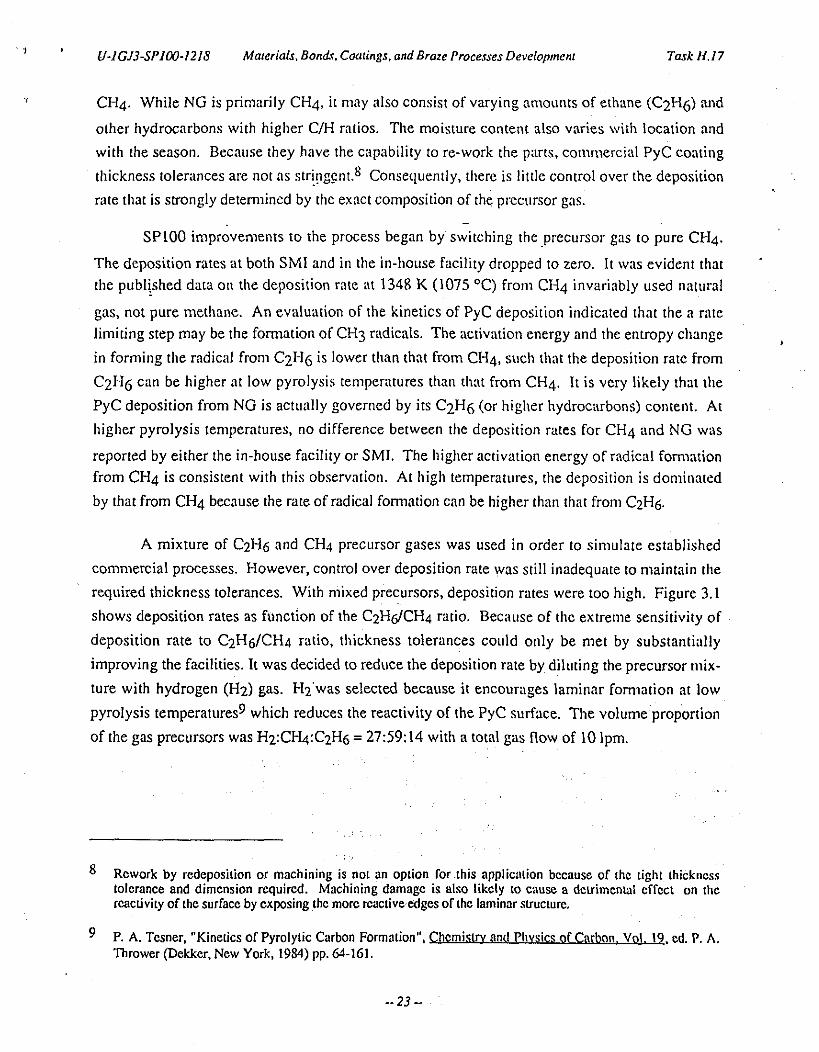
A mixture of CzH6 and CHI precursor gases was used i n order to simulate established commercial processes. However, control over deposition rate was still inadequate to maintain the required thickness tolerances. With mixed precursors, deposition rates were too high. Figure 3.1 shows deposition rates as function of the C2HG/CH4 ratio. Because of the extreme sensitivity of deposition rate to C2Hg/CH4 ratio, thickness tolerances could only be met by substantially improving the facilities. It was decided to reduce the deposition rate by diluting the precursor niix- ture with hydrogen (H2) gas. H2'was selected because it encourages laminar fomiation at tow pyrolysis temperatures9 which reduces the reactivity of the PyC surface. The volume proportion of the gas precursors was Hz:CHq:C2H6 = 27:59:14 with a total gas flow of 10 Ipm.
Rework by redeposition or machining is no1 an option Tor this application bccause of thc light thickncsr lolcrance and dimcnsion requircd. Machining damagc is also likcly to ciiusc a dcuimcnlal clrcci on thc reactivity of the surface by exposing thc morc rcactive edgcs or thc laminar svucturc.
P. A. Tcsner, "Kinetics of Pyrolytic Carbon Formation", Chcmistrv and Plivsics of Carb on. Vol. 19. cd. P. A, Thrower (Dckkcr. New York, 1984) pp. 64-1G1.
-- 23 -

U-IGJ3-SP100-121X rWareriaIs. Bondv. Coaiings, and Brazc Pr0cesse.r Dcvelopmenr
7 ,
Task H.17
Figurc 3.1 PyC Dcposiiion Ralc As A Funciion Of Prccursor G;IS Ratio
3.2.4 Pyrolysis Pressure
The PyC deposition rate increases with pressure. It is also possible that the character of tl~e PyC is affected to a large extent by the pyrolysis pressure. A detailed study of the deposition rnte as a function of pressure was deemed to be beyond the scope of this task. PyC coatings of acceptable characteristics deposited at 17 Torr had been demonstrated at SMI. This pressure wils used for all subsequent coatings.
3.2.5 Pyrolysis Temperature
, ., . . .
, , . . , , ,
, , , . . I
It was expected that the deposition rate was most sensitive to the temperature. Despite tlle sensitivity to the temperature, this was the parameter that was most difficult to nleasure ;uld coneol. Induction heating and packed graphite powder insulation employed in the in-house facility resulted in superior temperature control, over the resistive element heating and porous grapl~itc insulation employed at SMI. Attempts at SMI to control the temperature by manually adjusting the current input to the elements only resulted in irreproducible temperature-time profiles : ~ t ~ t l
variability in the deposition rate. A characterization of thefumace response and temperature-ti~nc profile was carried out at SMI.
-- 24 -

' 0-lCJ3-SPIW-1218 hiateriais. Bonds. Coatings. and Braze Processes Developnrenr Task 11.1 7
1110
1090
w 5 1070 !i k-5 a 2
1050
1030
1010
0 20 40 60 80 100 120 140 160 180 200 220 240
OEPOSITION TIME (MINUTES)
Figurc 3.2 Deposition Tcmpcriliurc Prorilc
It was determined that the response time of the SMI furiiace to changes i n the current setting were up to one hour and the response to the introduction of gas was greater than 3 hours. Figure 3.2 shows the temperature profile under the following conditions:
Preheat using a fixed current setting schedule for a total time of 105 minutes followed by a 30 minute cool down at acunent setting of 260 A; Introduce the gases at the end of the 30 minute cool down; Current input fixed at 260 A for the remainder of the run.
1)
2) 3)
The introduction of the gases results in a rapid drop in the temperature. The temperature never reaches equilibrium throughout the deposition run. If adjustments were made to the currcnt setting, as i n the usual practice, the temperature profile can vary over the range 1030°C to llOO°C. Since the deposition rate is higher at the higher temperatures, the thickness obtained would bc sensitive to high temperature excursions.
As shown i n Figure 3.2, a reproducible temperature-time profile can be obtained provitlcd the preheat conditions and the power input are fixed. The heat-up furnace current schedule is shown in Table 3.1. This schedule should produce a heat-up temperature-time profile such as !lint shown in Table 3.2. The deposition time required to obtain the 4 to 6 pm thickness was
:

1 ,
U-IGJ3-SPlIy)-1218 Materials. Bon& Coatings. and Brazc Processes Devclopmcnr Task H . I7
75
80
85
90
95 .
100
..-lo5 110
: 115 '
, , 120 "
125
130
35 . .
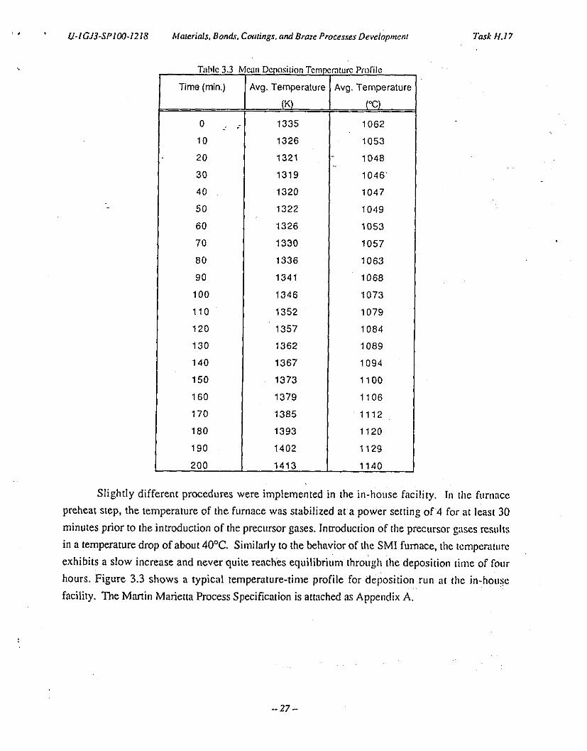
determined to be 167?2 minutes. The mean temperature-time profile during the deposition is shown in Table 3.3. A schedule of corrections to the deposition time for excursions above and below the mean temperature-time profile was developed. This is shown i n Table 3.4.
1272
1305
1337
, . ,1370,
1401
1425
, ' ,1438
. . '1441"
1413
1408
1405 . ,
Stari
EndlEegin I Soak End Soak
t-im Furnacc Ciirrcr
Time (min.) -
~-
0
10
20
35
55
75
90
105
105
135
:Ilctlulc
Robicon Current (Amperes)
50
160
240
310
330
330
330
330
260
260
'mpcralurc Profilc
Avg. Temperaturf ("c)
999
1032
1064
1097
1128
1152
1165
1168
1161
1150
1140
1135
1132
U-IGJ3-SPIW-I218 Malcrials. Bonds. Corrlings. (id Braze Processes Development Task H.17
Tahlc 3.3
Time (min.)
0
10
20
30
40
50
60
70
80
90
100
110
120
130
140
150
160
170
180
190
200
ilii Dcpixilion Tcm]
Avg. Temperaturf (K)
1335
1326
1321
1319
1320
1322
1326
1330
1336
1341
1346
1352
1357
1362
1367
1373
1379
1385
1393
1402
1413
aturc Prorllc
Avg. Temperaluri (“C)
1062
1053
1048
1046
1047
1049
1053
1057
1063
1068
1073
1079
1084
1089
1094
1100
1106
1112
1120
1129
1140
Slightly different procedures were implemented in the in-house facility. In tlie furnncc preheat step, the temperature of the furnace was stabilized at a power setting of 4 for at least 30 minutes prior to the introduction of the precursor gases. Introduction of the precursor gases results in a temperature drop of about 40°C. Similarly to the behavior of tlie SMI fumace, the tempcriiturc exhibits a slow increase and never quite reaches equilibrium through the deposition rime of four hours. Figure 3.3 shows a typical temperature-time profile for deposition run ii t the in-hoiisc facility. The Martin Marietta Process Specification is attached as Appendix A.
_ _ 27 __

U-ICJ3-SP100-12/S Maierials. Bondr. Coorings, u d llrazc Processes Devclopmenl
Table 3
Temperature
("c)
1025
1030
1035
1040
1045
1050
1055
1060
1065
1070
1075
1080
1085
1090
1095
1100
1105
1110
1115
1120
1125
Corrcclion For Temperature - Tim Profilc Dcviolions.
11-20°C . (min.)
0.6
0.6
0.7
0.8
0.9
0.9 1 .o 1.1
1.3
1.4
1.5 1.7
1.8
2.0
2.2
2.4
2.7
2.9
3.2
3.5
3.8
Time Correction
21-30 'C (min )
1 .o 1.i 1.2
1.3
1.4
1.6
1.7
1.9 2.1
2.3
2.5
2.8
3.1
3.4
3.7
4.0
4.4
4.8
5.3
5.8
6.3
3 1-40 ("C) (min.)
1.3 1.5
1.6
1.8
2.0
2.2
2.4
2.7
2.9
3.2
3.6
3.9 4.3
4.7
5.2 5.7
6.2
6.8
7.4
0.1
8.8
Task 11.17
3.3 PYROLYTIC CARBON MICROSTRUCTURE
It was found that the implementation of the new procedures at SMI also resulted i n improved strength performance of the MoGe bond.10 MoGe bonds tliat used PyC deposited wih the old process exhibited many failures in the PyC layer itself. This is believe to be caused by tlic
difference in the microstructure of the old vs. the new coatings.
lo R. Fcnton. "MoGc Bond Improvement Test Results" Princeton, NJ: Martin Marbkta Asvo Spacc: PlRll U- SPIOO-11.55, (SCP~. 1993).

, , U-IGJ3-SPIW-I218 Marcriuls. Bondr. Courings. und Braze Processes Devetnpmvli Task b1.17
Transmission (TEM) and Scanning Electron Microscopy (SEM) studies of the PyC coatings show that the average grain size of both old process and new process coatings is 25-35 A. The microstructure of the old process coatings, however, is interrupted by relatively large panicles, loo0 IO 3000 A in size. Such piirticles could have been caused by the dep;mures from temperature equilibrium during the deposition. The presence of these lirge pxrticles could be stress risers within the structure of the coating t h a t results i n reduced strength. The report on the characterization of the PyC coatings is in Appendix B.
. _
-
I140 i\ G
Figure 3.3 Dcposilion Temperature Profilc Tor llic I n - H o w Facilily
3.4 CONCLUSIONS
The character, mechanical strength, and thickness control of the PyC coatings were improved by exercising strict controls over the process and by minimizing operator intrusions. The SMI Facility could be improved by upgrading their gas handling system to use mass flow controllers specific to the precursor geses and the temperature nieasurenlent system to use themiocouples. The throughput at SMI can be improved by increasing the number of shelves within the reactor similar to that in the in-house facility.
__ 29 __

. , . , . . ."I ' . .' . .. . . , .
,. . , d.. ,

U-1 GJ3-SPIOO-1219 Morerials. Bondr. Coalings. and Bruze Processes Developinenr Task H.17
4. DEVELOPMENT OF Si3N4 COATING PROCESS
4.1 SUMMARY . -
A Si-rich silicon niaide (SiN,) coating is the reaction barrier between GS526 and graphite. There is significantly less crazing in SiN, coatings compared to stoichiometric Si3N4 coatings. Stoichiometric Si3N4 coatings are inv.viably in tensile stress in the as-deposited condition while the stress in SiN, is more compressive. SiN, also enabled the elimination of the S i02 coating betweenSi3Nq and (3526. Trappcd gases i n stoichiometric cl~eriiical vapor deposited (CVD) coatings of either Si-jNq or S i02 cause void formation at the interface with GS526. There is no void formation at the SiN, to GS526 interface because of reduced trapped gases and the presence
of unsaturated silicon bonds that strongly bond with GS526.
4.2 THE CHARACTERISTICS OF CVD S13Nq
-
4.2.1 Atmospheric CVD
Figure 4.1 shows stoichiometric Si3N4 deposited using atmospheric (ATM) CVD. There is extensive crazing in the coating. The growth morphology of CVD coJtings is nodular because the deposition initiates at nucleation sites -- if the growth rates iire not too anisotropic, these initiation sites grow outward into spherical nodules. The nodules on these specinien are suspected to initiate at cracks in the coating that have been covered up during the deposition. They also appear to follow a finer pattern of crazing in the films.
The deposition rate achieved with atmospheric CVD Si3N4 is very high. While this pro- cess is excellent for making thick films or bulk material, it is difficult to control for thin coatings ;it the 1 pm level. For the TA Cell, coatings are required IO be 1 to 2 pm thick. Severe crazing thnt eventually delaminates the coating, occurs i n thicker coatings. Another weakness of atmospheric CVD Si3N4 is its inability to deposit along the walls and bottom surfaces of the electrode grooves. The bottom and sides of grooves with dinlensions of .I6 x .40 x 1.0 that are part of the TA Cell design cannot be coated adequately at the same time as the outer surfaces.
4.2.2 low Pressure CVD Si3N4
Si-jN4 can also be deposited at low pressures -- about 200 mTorr. Low-pressurc. chemical vapor deposition (LPCVD) provide better control over the deposition thickness because the deposition rates are lower. There is uniform deposition on walls and bottom of electrodc grooves because the deposition process at low pressures is not controlled by diffiision, iind

U-IGJ3-SPIW-12lS Matcriols. Bonds. Coorings. and Braze Processes Dcvclopmenr Tmk 11.17
therefore is less sensitive to the exact geometry of the substrate. For the same reason, there is a
larger unifonrl deposition zone detemiiiied only by the iinifomiity of temperature and tlie f low rate of the precursor gases. The increased throughput overcomes the lower deposition ratc. There is also less particulate contiiriiinatioii i n LPCVD coatings because the deposition on tlie reactor walls are more adherent than that in atmospheric (ATM) CVD processes.
. -
Figure 4.1 Sloichiomcuic CVD Si3N4 Cmting
Figure 4.2 shows the LPCVD deposition of SijN4 on the bottom and the walls of a groove i n graphite of the same dimensions as that in the TA Cell Design. The deposition is uniform along the bottom and the walls. There is also little difference between surfaces that were oriented face- down and surfaces that were oriented face-up. As long as there is a large enough gap between the substrate and the walls, the deposition rate is unaffected. Tests indicate that this gap is a t least as small as 0.41 mm (0.016 in.), the width of the grooves in the test module.
LPCVD Si3N4 coatings also exhibited reduced crazing. Figure 4.3 shows the surface of LPCVD Si3N4 coating on graphite. Although stoichiometric Si3N4 could be made by LPCVD in much the same way as in ATM CVD, these samples were slightly silicon rich.

' . U-lGJ3-SP1OO-I218 Muieriuls. Bondr. Cou1ing.r. and Brim Processes Development Tusk H.17
Figurc 4.2 LPCVD Si3N4 Coaling at Bottom of Elccuodc Groovcs
Figurc 4.3 Surfacc of LPCVD Si3N4 Coating on Graphite

U-ICJ3-SPIOO-1219 hfuteriuls. Bonds. Coorings, and Braze Processcs Derclopmcnr Task 11.17
4.2.3 Stoichiometric Si3N4
N/Si ratios greater than 20 i n the precursor gas mixture are required to produce coatings with the correct stoichiometry. Ratios of tip to 10000 have beeti reported ;IS producing fully stoichiometric materia1.I' A1thoUgt;the N/Si ratio is stoichiometric, the s t ruc t i~r~ is usually far from perfect. In addition to the Si-N bonds of a perfectstructure, Si-H and N-Id bonds are also found. At low N/Si ratios of the precursor gas, the coatings are Si-rich with excess Si bonds temiinated with H, that is Si-H bonds. As the N/Si riitio is increased, N-H bonds are ;dso fomied unt i l the stoichiometric composition is produced. Figure 4.4 shows the Si-H and N-H contcnt obtained by optical density nieasurements for coatings made with varying N/Si ratios i n the precursor gas. While the Si-H remains relatively constant, the N-H rises as the N/Si ratio increases.12 Heat treatment at 1 l 0 O T releases the hydrogen gas.
X ,0.4 Torr 7" I- - iij
n z W
IO I- -1
NHS / S i H2 C Figure 4.4 Si-H And N-H C
' I W. Kern and V. S. Ban. "Chcmical Vapor Dcposiiion of Inorganic Thin Film". in Thin Film P r m ' . ELIS.
L. Vosscn and W. Kern. (Acadcinic Prcss, Ncw York. 1978) pp. 258-331,
T. Makino, "Composiiion and Siructurc Convol by Sourcc Gas Ratio in LPCVD, J. Elcctrocllcin. Soc.. Vol. 130. No. 2 (Fcbruury. 1983) pp. 450-5.

U.-IGJ3-SPIOO-1218 Mareriols. Bonds. Coorings, ond Braze Processes Devclopmcnr
4.3 GLASS BONDING TO S13Nq
4.3.1 Sloichiometric CVD SijN4
Task I I . I7
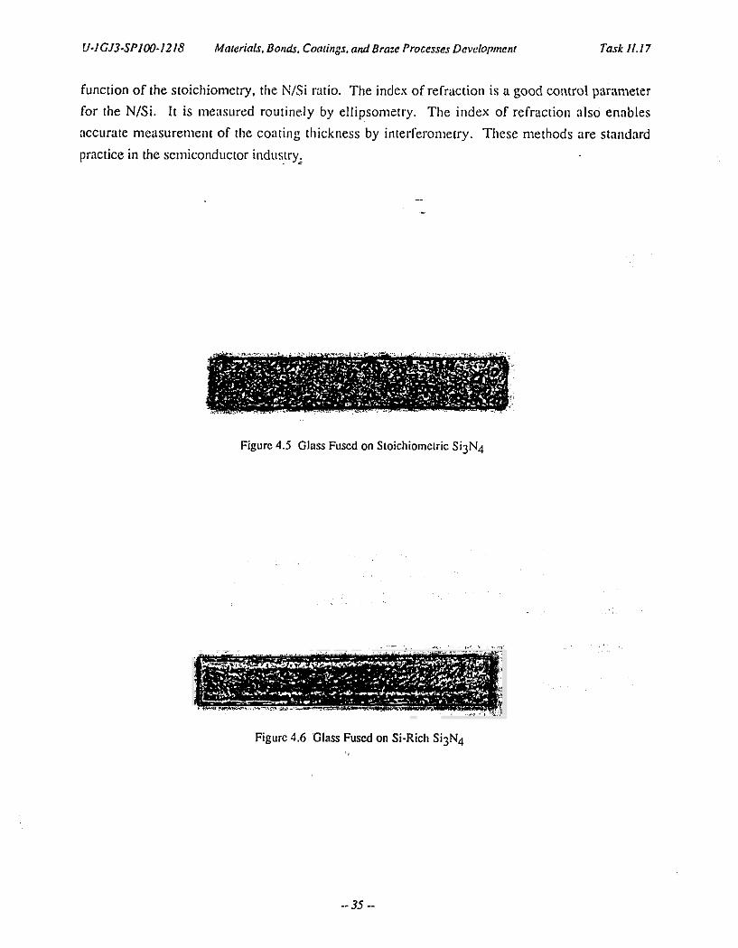
Previous attempts to bond GS526 glass directly to CVD Si3N4 were unsuccessful. Bubbles formed at the interface. Without an applied load during glass fusing, as in perimeter glass fusing, severe blisters were formed. Figure 4.5 shows the-surface arid cross section of glass fused on stoichiometric CVD Si3N4 without ;in applied load. The blisters are evidently caused by large amounts of hydrogen gas being released during the fiisiiig operation.
The MOD-RTG program that used GS.526 perimeter glass not only fused the perimeter glass under load but also applied an overcoat of CVD Si02 in order to minimize the bubble form;ition at the interface. This method had very limited success when attempted i n the SPl00 program. I t is now clear that the Si02 overcoat alone was not the real reason the blistering \vas reduced in the MOD-RTG program. It is more likely that the deposition of Si02 at about 400°C released some of the hydrogen gas trapped in the N-H bonds; and this minimized the gases released during the glass fusing operation. It is unlikely, however, that all the trapped hydrogen gas was released at 400OC; and, this led to the limited success of the Si02 overcoat when the glass is fused without any load.
4.3.2 Si-rich SIN,
CVD SiN, using low N/Si ratios in the precursor gas mixture produced coatings with low
hydrogen content. The Si-rich coatings also contained unsaturated silicon bonds, giving i t a Si- like character. Hence, GS526 should bond strongly to SiNx just as it does to a pure silicon or SiGe surface. Figure 4.6 shows the surface of GS526 fused on a SiNs coating. Note the abscrice
of any bubble formation.
4.4 CONCLUSIONS
4.4.1 CVD SiN, Specifications '. ,. .
Figure 4.7a shows the N/Si ratio in the coating as a function of the ratio of precursor gases.13 The figure shows how the ratio approaches 1.33, the stoichiometric ratio, as tlic precursor gas ratio increases. In Figure 4.7b, the index of refraction of the coating is shown as
U~ICJ3-SP1OO-IZ 18 Mnteriu1.r. Bondc. Coatings. and Braze Processes Dcvdopmcnt Task 11.17
function of the stoichiometry, the N/Si ratio. The index of refraction is a good control parameter for the N/Si. It is niensurcd routinely by ellipsonietry. The index of refraction also enables accurate niensurenient of the coating thickness by interferometry. These methods arc standard practice in the scmiconductor industry, .~
. . ~ ,~ .. . . . . ..
Figurc 4.5 Glass Fuscd on Stoichiomctric Si3N4
Figurc 4.6 Glass Fuscd on Si-Rich Si3N4 I,
1

N ATOM
SI ATOM
IO.' I IO NHJSiHzCtz RATIO
I
1.911 I ' 1 ' 1 ' 1 ' 1 I I 0.5 I 1.9
N/Si R A T I O
Figure 4.7 (a) SI and N Conccnlralion as a Function or Prccursor Gas Ratio
Figurc 4.7 (b) Rcfraclive lndcx oTSi3N4 Coatings as a Function or N/Si Ratio.
Si3N4 coatings with a N/Si ratio of 1.0 to 1.1 exhibited no criizing on SiGe substr:ites :illd only slight crazing on graphite substrates. This range of N/Si ratios was more than adequatc 10 prevent blister formation at the interface with CS526. According to Figure 4.7b, the indcx of refraction of coatings with this N/Si ratio is 2.15 to 2.25. The specified parameters of SiN, are:
Index of Refraction: Thickness:
2.15 to 2.25 1 .O to 2.0 pm
The SPlOO Specification for SiN, and Si02 coatings is in Appendix C.


U-lGf3-SPIW-12 18 hfaleriuls. Bondr. Coalings. and Braze Processes Dcrelopmenf Task 11.17
5. DEVELOPMENT OF COMPOSITE GLASS LOW VOLTAGE INSULATOR
5.1 SUMMARY
The SPlOO lateral glass is a gl:iss-ceroniic developed froin the parent GS526 composition by incorporating Si3N4 -reinforcement particles. The composite has Iiiglier fracture toughness and themial conductivity than the parent GS526 alone. The improved fracture toughness enabled a fail- safe TA cell design which was not possible using the parent GS526 g1;iss.
5.2 TA CELL DESIGN REQUIREMENTS
. *
L
5.2.1 Electrical and Thermal Requirements
The primary function of the lateral glass is to electrically isolate the thermoelectric legskouples from each other. Because of its location, i t is also in series with the High Voltage Insulator (HVI) in isolating the module from ground (but the dielectric strength of the HVI is mandatory to complete that function). The lateral glass must have high electrical resistivity at service temperatures. Because the lateral glass is in the thermal path, another general requirenicnt is high thermal conductivity. The specified reference lateral glass material is GS526 which had been used in the MOD-RTG program. Because of the fixed electrical and thermal properties of GS526, a lateral glass thickness was specified which represented a compromise between the electrical and the thermal requirements. The specified thickness was 50 pin (0.002 in.), similar to thicknesses that were achieved in the MOD-RTG prosram. Because of the different hardware dimensions of the TA cell, however, it was necessary to modify the glass fusing process in ordcr to achieve this thickness.l' I t was shown that the practical thickness limit achievable using GS526 was ,002 inch. Cell performance calculations depended on the following GS526 properties: 15
* Thermal Conductivity, A = 0.02 (W/cm-K) Electrical Conductivity, cs = 1.4 x 10⁶ (Shcm)
l4 J. M. Rcycs.'"Bond Thickness TCSIS" Princclon. NJ: Marlin Maricita Asiro Spacc: PIR # U-SP100-445
l5 J. A. Bond, "TA Ccll Design Dcscriplion and Developmcni Stalus" Princclon, NI: Marlin Maricua hsiro S ~ X C : PIR # U-1L8.5-SPlOO-1214. (31 MX Y4).

U-ICJ3-SPIW-IZIS hlarerinls. Bon& Conrings. and Braze Proccr.m Dcvclopmenr 7ask 11.17
5.2.2 Fracture Toughness Requirement
In tlie fracture mechanics approach to cell design, the lateral glass must have a critical crack intensity, Klc, that is higher than 1.2 MPa-diii (1.1 ksidin) I f K l c is lower, then the design is
not fail-safe; that is, cracks may procophgtite should there be flaws ;it the edge of the glass. Cracks are certain to occur in brittle materi:ils because they will have flaws ii t the edges. This is [he difference in behavior between brittle and ductilc materials. With a K l c higher than 1.2 MPa&,
the flaws at the edge of brittle materials will not propagate nnd the desizn is fail-safe.
5.3 COMPOSITE GS526
*
The measured fracture toughness of GS526 was only 0.604 MPaedm (0.55 ksidin). This value precluded :I f:iil-safe cell design without major revision. Considering schedule and funding constraints, development of a new lateral glass system was impractical. Even i f a glass system with high fracture toughness could be found, it would most likely be quite different from the GS526 composition and would require extensive qualification.
GS526 fused at 1473 K (1200 “C) is already a glass-cernmic.16 Although no fracture toughness data exist for GS526 fused at lower temperatures, it would be expected to be lower than that of the 1473 K fused material because of the toughening properties of the crystalline phases. Fusing at 1473 K, there is more complete devitrification and stabilization of the microstructure. The crystalline components function as reinforcement in the glass matrix structure placing the material in compressive stress. Compressive stress tends to close cracks, reducing their tendency to propagate. In fusing plain GS526, the segregation of the components of the glass is not controlled and the toughening of the glass-ceramic structure is less than optimal. One reason is that the difference in the coefficient of thermal expansion (CTE) between the crystals and the glassy matrix may be Small, with a concomitantly small residual compressive stress field. One method of toughening GS526 is to incorporate particle reinforcements, by design, to enhance the compressive stress field. The requirements for tlie particle reinforcement are:
l6 D. Bloyer, “Currcnt S u u s of Ihc GS526 Material.” Princclon, NJ: Martin Marictln Asiro Spacc PIR# U-IR7S- SPIOO-853, (16 Jan 91).

U-IGJ3-SPlW-12I8 Marerials. Bonk. Coulings. and Braze Processes Developmenl Task 11.17
(1) The CTE must be sufficiently different from that of GSS26. A lower CTE is preferred because the lower composite CTE will increase the safety margin of the TA cell against failure at the SiGe.
(2) The elastic modulus musi b i similar to, or higher than t h n t of GS526. Otherwise. tlie
composite CTE will be governed by the component - with tlie higher modulus; and, to lower the CTE, it may required a large amount of reinforcement added.
(3) The reinforcement material must be thermochemically stable with the components of GSS26. Any major reaction that occurs between GSS26 arid the reinforcement may alter the properties of the composite.
The pcuticle size of the reinforcement cannot be larger t1i:tn ,001 (25 p i ) . This is to ensure that the specified thickness of .001 inch is achievable.
The electrical resistivity of tlie reinforcement material must be higher than that of GS526. There is a trade-off here between the electrical resistivity and the tlieimal conductivity. The lower electrical resistivity may be accompanied by higher themial conductivity. If so, then a lower elecmical resistivity may be accommodated in the TA design by making the lateral glass thicker with some sacrifice in the potential improvement in the themid conductance.
An important requirement for the particle reinforcement was availability. The material had
(4)
(5)
to be readily available to permit development and testing within the program schedule constraints.
5.3.1 Coefficients of Thermal Expansion
The CTE of Si3N4 according to the TPRC TablesI7 is shown i n Figure 5.1. The CTE of the cast material between 273 and 1273 K (0 and 1000 "C) is about 2 . 3 ~ 1 0 6 K-1. From the same
source, Figures 5.2 and 5.3 show the CTE of Si and Sic, which have an average CTE over the same temperature range of 3.7~10-6 K-1 and 5 . 3 ~ 1 0 6 K-1, respectively.
17 T h c r m o o h v ~ c rties of Hieh Tcmocraturc Solid Metc .rials, cd. by Y. S. Touloukian, Thcrmophysicnl Propcrties Research Centcr. Purduc Univcrsily. New York: MxMillan & Co. (1967).
-_ 39 --

. . Task 11.1 7 U-IGJ3-SPIO-12I8 MureriaD. Bonds. Coarin~s. and Brure Proce.y.rcs Dcvclop~~~cnr
r." .,...., ",. I.,,
- 1 i i ;I 3 f -
r
f i
r..,* ..I",.. .%
Figurc 5.1 Codficicnt of Thcnnal Expansion of Si3N4
I..-..Y... .I
nlcr-r.. .n
Figurc 5.2 Cocfficicnt of Thermal Expansion of Si

Task H.17 U-1 G/S-SPlW-lZIS Morerink. Bondr. Courings. and Brure Processes Drvelopment
Figurc 5.3 Cocfl'icicnt oTThcrm:il Expansion of Sic
5.3.2 Reinforcement Material
Si3N4 and Si were initially selected as possible particle reinforcements. S i c was included in the evaluation as an alternative if fracture and stress analysis require a toughened glass with essentially the same or higher CTE than GS526. As a refinement of the composite glass development, mixtures of these particle reinforcements were also considered. The main criterion for the selection at this stage was reinforcement compatibility with the components of GS.526. Other higher CTE materials considered -- but not pursued -- were AIN, tungsten, and tungsten carbides. Other materials could be considered if further increase in CTE were required.
Initial work was limited to Si3N4 reinforcement. It was preferred becuase it was known to be inert. The MOD-RTG experience with bubble formation at the interface between GS526 and Si3Nq is limited to CVD Si3N4 coatings. No similar reaction was expected between GS526 and bulk Si3Nq powder. Work 011 Si reinforcement was discontinued when i t was determined that its elechical conductivity at service temperatures might lead to low isolation resistance.

U-IGJ3-SPla)-IZI~Y Marcriafs. Bonds. Coarings. and Brare Processes Deve/opnreni
Material
GS-526 (cycled) 35 v% Si3N4
50 v% Si3Nq
Task H.17
K I c CTE Modulus
(MPadm) ( 1 / K ) @Pa) 0.60 4.67~10.~ 76.5 1.65 4.19x10*6 137.2
3 . 8 6 ~ 1 0 . ~ 107 .5
5.4 RESULTS
Material
GS-526 (cycled) 35 v% Si3N4
50 v% Si3Nq
Two compositions were made: 35 and SO volume % Si3N4 i n GS526 glass. The proper-
ties of the composite glass are shown in the Tablc 5.1. The gl:iss-ceramic resulting from the SO% composition hod high porosity, due tdthc high effective viscosity at the fusing temperature of 1473 K (1200 "C). The high viscosity also iiiearit that the thickness requirement could not be met.18 The effective viscosity of the 35% composition was 1ower;nnd a minimum thickness of the glass- ceramic of 75 pni (0.003 in.) was achieved -- better, but still higher than the requirement for GS526. However, since the thermal conductivity of the composite glass is higher than that of the parent GS526, the ni:iximum acceptable lateral glass thickness incre:ises to 91 ,um (0.0036 in.), so the 75 pm thickness represents an improvement in thermal conductance over the parerit GS-526.
-
Resislivity Resistivity at 073 K at 1273 K
(Q-cm) (nacm)
1 .8Ox1O9 6 . 8 0 ~ 1 0 6
2.02~109 7.12~105 _ _ - -
ai 873 K
The electrical resistivity at 1273 K (lOOWC) WBS slightly lower than that of GS526 but still acceptable. The resistance of lateral glass 2.54x2.54 cm in area and 75 pm thick (1~1~0.003 in.) was estimated as 560 MQ. This three-fold increase in fracture roughness over the parent GS.526 enabled a fail-safe cell design. The fracture toughness exceeded the requirement of 1.2 M P a h by a comfortable margin.
J. M. Reyes, "Bond Tliickncss Tcsts." Princcton. NJ: Marlin Marietta Asuo Spacc PIR# U-IRTI-SP100-445..

U-1GJ3-SPloO-IZIS Mareriols. Bond. Coaiings. and Braze Processes Devclupnicnr Task Ii.17
6. DEVELOPMENT OF A 1200°C BRAZING ALLOY
6.1 SUMMARY _. *
An alloy consisting of 56 weight percent (w/o) zirconium - 28 w/o vanadium - 16 w / ~
titanium (Zr-28w/oV-16~v/oTi) was developed for high teniperature brazing applications in the SP- 100 themioelectric cell and heat exchanger. The alloy was used successfully to bond the thermoelectric cell to the heat exchanger, the compliant pad to the insulator assembly and the compliant pad to the module.
6.2 ALLOY SELECTION
The initial application for a high temperature braze was the bond between the themloelectric cell and the heat exchanger. Braze requirements were developed from an analysis of the design requirements for the bond. These required a braze that:
melts at a temperature below 1473 K (1200 "C); contains elements with low vapor pressure at the operating conditions of 1350K (1077 K) and 10-6 Torr; and contains elements that wet and are compatible with the niobium facesheet of the insulator and the niobium - 1% zirconium alloy of the heat exchanger.
*
The literature was searched to determine if any high temperature commercial braze alloys existed which met the above requirements. No such alloys were discovered. The next step was to examine existing binary and ternrtry phase diagrams for low vapor pressure element combinations which could meet the melting point and compatibility requirement (no brittle intermetallics) with niobium. From this search, ten possible alloy combinations were selected as follows:
1. 2. 3. 4. 5. 6. 7. 8. 9. 10.
zirconium - 30 w/o vanadium zirconium - 30 w/o vanadium + 2 w/o silicon zirconium - 30 W/o vanadium + 4 WJo silicon zirconium - 30 w/o vanadium + 6 w/o silicon zirconium - 28 W/o vanadium - 16 w/o titanium zirconium - 28 W/o vanadium - 16 w/o titanium + 2 w/o silicon zirconium - 28 W/o vanadium - 16 W/o titanium + 4 w/o silicon zirconium - 28 W/o vanadium - 16 W/o titanium + 6 w/o silicon 48 w/o zirconium - 48 W/o titanium + 4 W/o silicon titanjum - 30 w/o vanadium + 4 w/o silicon

U-lGJ3-SPIOO-12 18 Malerials. Bonds. Coatings. and Braze Processes Devcloptncnt Task 11. I7
Small buttons (approximately 755) for each alloy composition were prepared and melted in a vacuum arc fumace at General Electric Corporate Research and Dcvelopnient (GE-CRD) Center in Schenectady, NY. The melting points of each of the alloys were then measured by Differential Thermal Analysis (DTA). Only the _ _ -. Zr - 28 w/o V - 16 w/o Ti family of alloys exhibited melting points less than 1473 K (1200 "C).
- At this point, i t was necessary to fabricate the alloys into a foil form that could be used for
brazing. Initial investigations to find a vendor to roll the alloys down to a thickness of approx- imately 50 pni (0.002 in.) were not successful.
Attempts were made to Pabricate braze foil using a melt spinning technique (metallic glass foil) at METGLAS, Inc. Three alloy compositions were tried: Zr - 28 w/o V - 16 w/o Ti; Zr - 28 w/o
V - 16 w/o Ti + 4 W/o Si; and Pt - 3 w/o B. The latter alloy was chosen based on an article in the extemal literature which stated that this alloy tiad been used successfully to braze refractory metals. The melting point of Pt-3B was also reported to be approximately 1073 K (800°C).
The METGLAS spinning technique was not successful in producing foil for the Zr-28V- 16Ti + 4W/, Si or the Pt-3B alloys. The alloys were too brittle and broke into small chunks during the spinning process. Foil ranging i n thickness from 25-75 pni (0.001-0.003 in.) were produced for the Zr-28V-16Ti composition by METGLAS.
Initial brazing trials were then performed with the Zr-2SV-16Ti foil and Pt-3B which had been ground into a fine powder. The foil and the Pt-3B powder were placed between a pure niobium foil and a niobium - 1% zirconium (Nb-l%Zr) plate and heated to brazing temperature to simulate the thermoelectric cell to heat exchanger bond. The Pt-3B alloy would not bond successfully to the niobium foil and the Nb-l%Zr plate. The bond separated easily after removal from the vacuum brazing furnace and exhibited low tensile strengths (2.8 MPa/400 psi). On the other hand, the Zr-28V-16Ti seemed to form an excellent bond between Nb and Nb-l%Zr.
6.3 ALLOY CHARACTERIZATION AND INITIAL SP- 100 EXPERIENCE
The braze samples with the Zr-28V-16Ti foil were subjected to mechanical property (tensile) testing. The bonds exhibited greater than 28 MPa (4000 psi) tensile strength which was considered acceptable by the thermoelectric cell designers. Metallographic examination showed that the braze did not exhibit any evidence of cracking or voids. The braze alloy wet both the niobium and the niobium - 1% zirconium and no brittle intermetallic compounds were detected.
, I
Physical and other mechanical property measurements were then made to characterize the

U-1 GJ3-SPIOO-IZIS Muferinls. Bondr. Coorings. and Brazc Processes Dcvelopmcm Task 11.17 ' .
Zr-28V-16Ti alloy. The measured density was approximately (i.Og/cc. The melting range of the alloy was determined to be between 1423 and 1453 K ( 1 150-1 I80 'C) using DTA. A remelt temperature of Trclnclt > 1673 K (1400 "C), for the Nb/Zr-28V-IGTi/Nb-lZr bond, w:is detemiined by hanging a weight from bonded . samples i in the vacuuni fumace and recording the temperature at which the bond separated. The coefficient of themial expniision w:is measured19 as 9.62x10⁻⁶ K-1 by GE-CR&D. The. measured elastic modulus was 1 4 . 2 ~ 1 0 ~ psi at room temperature20 with a Poisson's ratio of 0.36. The measured themial conductivi?y2' of tlie alloy W;IS 0.237 W/cm.K at 873 K (600 "C) and 0.254 W/cm*K at 1873 K (1600°C).
The first application of the Zr-28V-16Ti braze foil was to bond the PD-1 cell to the heat exchanger. A brazing cycle of 1473 K (1200 "C) for 6 minutes was used with a fast ramp up and a slow cool down. The braze metal was pieced together with four 2.54 ciii (1 inch) long strips laid between the Nb-l*/,Zr heat exchanger and a Nb-l%Zr strong back, which is a structural support used to prevent deflection of a test anicle. Both surfaces were acid etched prior to brazing.
The braze was successful for the PD-1 application. The post-test analysis showed that the braze melted and wet both surfaces well. Approximately 80 to 90% of the area was covered by the braze and voids were only present where strips were adjoining each other. The braze was also successfully used for the PD-2 cell application. This cell also contained a Nb-l%Zr strongback and both the strongback and heat exchanger were acid etched prior to brazing. This cell was never tested due to a module crack and the braze was not examined in tlie post-test an;ilysis.
The Zr-28V-16Ti braze was next used to bond the Nb-I%Zr heat exchanger to the N b facesheet on the insulator assembly for the PD-2A Pathfinder cell. The braze was again pieced together in strips and the some time/temperature cycle was used. The heat exchanger was again acid etched; the niobium facesheet on the insulator was only chemically cleaned with a solvent. The PD-2A cell exhibited a large parasitic temperature loss on the cold side. Post-test analysis showed that the cold side braze had only 10% of the area brazed. The braze did melt and wet the cold side heat exchanger. The braze did not wet the niobium facesheet. Failure of the braze was attributed to three causes:
l9 Princeton. NJ: Manin Marietta ASUO Spacc PIR# U-IRTI-SP100-10X9 (Novcmbcr 10. 1992).
2o Princeton, NJ: Martin Marietta Astro Space PIR# U-1RT1-SPIOO-1093 (Dcccmber 22, 1992).
21 A. Robison "Lascr-Flash Results Cor Zr-ZXV-16Ti Braze" Princeton, N1: Martin Maricua Astro Spxc mcmonndum (February 25, 1993).

(I-1 GJ3-SPlOo-I2lS Materials. Bondy. Coatings, and Braze Processes Dcvelopiirenr Task I I . I 7
1 . The Zr-28V-16Ti braze did not wet non-acid etched niobium
2. A large gap (75 to 100~1/.003-.004 in.) existed between the heat exchanger and cell. The braze is sluggish at 1200°C and does not readily flow to fill the gap
The METGLAS foil was extremely variiible in width and thickness. Thickness range vaned between 25 pni and 75 pni (0.001 - 0.003-in.)
.. - 3.
As corrective action, a procedure was developed to acid etch the niobium facesheet of the insulator and an alternare source for unifomi Zr-28V- IGTi braze foil was investigated.
6.4 ROLLED Zr-28V- 16Ti AUOY FOIL
Two methods of producing a uniforni width and thickness of Zr-28V-IGTi braze foil were investigated. The first method was to produce a braze foil using thc high rate sputtering technique developed by the Battelle Memorial Institute in Richl:iiid, WA., to produce compliant pad facesheets. A Zr-28V-16Ti target was used to sputter 50-75 pni (.002 to ,003 in.) of the braze onto a copper substrate. The copper was leached away to produce ii uniforni thickness braze foil
Brazing trials using the sputtered foil were nor successful. The foil contained large voids from trapped gases (Kr, Xe) used during the sputtering process. Poor bonds with low tensile strengths were obtdined and further effort on sputtered foil was terminated.
The second method for obtaining uniform thickness braze foil was by hot/cold rolling. Two vendors attempted rolling the remainder of the Zr-28V-16Ti ingot produced by GE CRGrD. Fine Metals in Richmond, VA., was unsuccessful, however, Microfoils, Inc. of Burr Ridge, IL., was successful in producing Zr-28V-16Ti braze foil of 50 to 75 pni (0.002-0.003 in.) uniform thickness. Brazes using this foil had excellent wetting characteristics and high tensile strengths. The braze foil was also produced in widths greater than 25.4 mm (1 in.) avoiding the need to piece together foil strips. The melting point of the rolled foil was confirmed to be 1423-1453 K (1 150- 1 180 "C) by DTA.
Processing of the ingot into foil at Microfoils involved sealing the alloy in stainless steel and heating to be a temperature of 1173-1273 K (900-1000 "C) under an Ar atmosphere. The can was hot rolled to obtain a 1.27 mm (0.050 in.) sheet of Zr-28V-l6Ti, without evidence of crack- ing. Rolling the alloy at an intermediate temperature of 873 K (600 "C) reduced the alloy to ;I
thickness of 0.25 to 0.50mm (0.010 to 0.020 in.), after which cold rolling was used to reduce the foil to its final thickness. The foil was annealed after each rolling reduction of 50 to 75%.

(I-IGJ3-SPIOO-12 18 Mafcrials. Bond& Coalings. and Braze Processes Devclop~ncnr Task 11.17
Application of the rolled braze foil w;is made to the TA cell to heat exchanger bond. The brazing operation was performed at a temperature of 1200 k lO0C for 15 minutes at LL pressure of 0.18MPa (25 psi). The braze foil wet both surfaces (which were acid etched) and achieved an excellent bond which was confirmed by port-test analysis. _.
Because of the stiffening problcni on diffusion bonded - compliant pads22, studies were undertaken to use the rolled Zr-28V-IGTi braze foil to bond the compliant pad to the insulator assembly and the conipliant pad to the cell module assembly. For the compliant pad to insulator assembly, a 50 pm thick (0.002 in.) braze foil was used. The brazing parameters were the same as those used for the heat exchanger bond. The braze foil did an excellent job of wetting and bonding the niobium facesheet of the insulator arid the 75 pni thick (0.003 in.) niobium facesheet of the compliant pad.
-
'
For the compliant pad to module assembly bond, the braze foil was further rolled to a thickness of 12.51.1 (0.0005 in.) by Microfoils. This thin foil was still able to wet the 12.5 pin (0.0005 in.) thick niobium facesheet of the compliant pad its well ;IS the 25 pni (0.001 in.) thick perforated tungsten foil on the top of the module assembly. Because of the sluggishness of the braze at 1473 K (1200°C), the Zr-2XV-lGTi braze will wet and bond to the tungsten foil without flowing into the holes. Brazing parameters used were again the same as the heat exchanger bond.
Post test evaluation of the TA cells has indicated that the Zr-28V- 16Ti braze has performed well in this application. The alloy was used successfully to bond the themioelectric cell to the heat exchanger. the compliant pad to the insulator assembly, and the compliant pad to the module.
22 J.A. Bond, "Lessons Lcarncd in Devclopmcnl and Tcst of Convcrtcr Tlicrnioclccvic Ccll." Princcton, NJ: Martin Marictta Astro Spacc PIR# U-SPIOO-1212. (31 May 1994).

. _-
!
1 ' .

Characterization of Pyrolytic Graphite Coatings
Prepared by:
David McNamara
Martin Marietta Laboratories 1450 South Rolling Road
Baltimorc. Maryland 21227
September 24, 1993

, .. ~.
. . I .
.. . .,
. i
. ..,..{. . . . I , . . . i , . I

I. Introduction
ID # Process Run Thickness (pm) S3517-71 old 45 7.6-9.2 ET4249-3 old 63 2.5-3.4
-S3517C-153 new 89 7.2-9.2 ET4249-11 new 89 7.2-9.4 ET4249- 14 new 96 4.2-5.0
Graphite substrates pttpared with pyrolytic graphite coatings have shown a propensity for mechanical failure in the coating. The pyrolytic coating is applied from a Methane:Ethane:H2 gas mixtureat approximately 1080°C. A modificauon in process procedure was made that has improved the coating properties. Temperature control of the process oven was formerly tied to an optical pyrometer monitoring the substrate temperature. However, due to the large thermal massaf the system, this lead to poor temperature control. Current practice is to use a fixed power setting and adjust gas flow to control the temperature profile, which has proven to provide better response.
- - The purpose of the investigation detailed in this report was to identify techniques
that could be used to characterize the pyrolytic coatings, and identify the reason for the differences in mechanical behavior. Three primary techniques were used to characterize the coatings; X-ray Diffraction (XRD). high-resolution Scanning Electron Microscopy (SEMI. and Transmission Electron Microscopy (TEM). The difference between coatings applied in the new fashion compared to the old are very slight. It appears that more rapid grain growth and the subsequent formation of some larger crystallites took place in the coatings formed by the prior technique. *.
11. Sample Identification
ID. X-ray Diffraction
A Scintag Pad V diffractometer was used to characterize the thicker coatings on largersubstrates, Le., S3517-71 and S3517C-153, runs 45 and 89 respectively. These samples were best suited to XRD. since the thicker coatings would produce stronger signals from the coatings, and minimize the effect of-the substrate. Standard diffraction scans shown in Figure 1 indicate that the majority of the signal still comes from the substrate, however. The sharp peaks clearly come from the substrate material. There is a significant broad shoulder at the base of the 002 peak (26.5'). Figure 2 shows an
Technical Repon Characterization of Pyrolytic Graphite Coatings September 24,1993 1

expanded view of the scan around this peak. The very broad shoulder represents very fine-grained crystals in the coating layer.
Grain size can be determined in XRD by determining the half width of the peak and applying the formula' .
x- m y wavelength grain = peak half-width cos(8) -
where 0 is the angle of the peak center. The wavelength of characteristic Cu x-ray line used is 1.54178 Angstroms. From Figure 2 the approximate peak half widths are 2.8 degces (0.436 radians) for both coating specimens. Thus the approximate grain size is 35 Angstroms.
..
To better determine if there is any difference between the broad coating peaks, the scan values for the substrate were scaled and subtracted from those of the coatings. and plotted in Figure 3. The discontinuity on the right side of the peaks is due to misallignment between the background and coating scans. It is clear that, aside from a difference in height, there is no significant difference in peak shape for the two cases. This difference probably reflects a difference in coating thickness.
Rocking curves were also collected around the 002 peaks. An early paper2 noted differences in the rocking peak width, Le.. differences in degree of basal plane order, as a function of heat treatment temperature. Figure 4 shows the results for the three cases. There is no difference between the substrate and the coating side of Run 89425. There may be some difference in the right hand side of the scan from coating Run -#3. It appears that the intensity of the substrate peak is overwhelming the potential information of the x-rays reflected from the coatings. Development of this technique would require either the removal of the substrate material, or growth of coatings on amorphous substrates or substrates of materials that do not have strong XRD peaks around 26 degrees 20. ... -
.~ . -. . ,
. .. .. .
IV. Scanning Electron Microscopy
Two types of high resolution SEM were performed on selected samples. High magnification photomicrographs were taken of coating surfaces, to see if grain size and orientation might be seen on the surfaces. Photomicrographs were also taken of fractured cross-sections of coating samples to,,examine the layer Structures of the coatings. A JEOL IOOCx STEM was used in the scanning, secondary electron mode to examine the specimens. This instrument is particularly suited to high resolution SEM as it uses a lens prefocus scheme to for" very small probe beams, and'it shields the electron detector
, . . , .
,i
, .
'Z.G. Pinsker, Electron Diffraction, Bunenvorths Scientific Publications. 1953. p. 202. *O.J. Guenter and S. Cvikevich. in Roc. 51h Carbon Conference, Pennsylvania Stale University, (MacMillan. I iY) 1961.pp473-481.
Technical Report Characterization of Pyrolytic Graphite Coatings September 24. 1993 2

from backscattered electrons that add background "noise" to the signal in conventional SEMs.
Figure 5 shows the coating surface of an old-process, thin coating, Run 63-#24 at 5 0 , o O X . The main features Ke-small (0.3 - 0.8 micron diameter) pores. The general surface also has a bumpy appearance, with features about 0.1-0.2 micron. The surface of an new-process, thin coating, Run 96-#92. shown in Figure 6, also has a fine pore structure. Except for the pores, the general surface appears smoother than 63-24. Finally, Figure 7 show a photomicrograph of a new-process, thick coating surface. Run X9-#44. Here the pores cover a wider size range (0.3 - 1.2 micron) with more large ones. The-darker spheres in the figure are sitting on top of the surface. Once again. the general surf& is quite smooth.
Photomicrographs of the coating cross-sections are shown in Figures 8 & 9. The old-process, 63-24, coating, Figure 8, has very thin layers parallel to the substrate surface. The "banding" seen on the fracture surface suggests that there may be secondary interfaces between groups of layers. The fracture surface of the new-process coating, 96- 92, Figure 9, also has very thin layers that appear more uniform across the thickness.
_. When viewed at an oblique angle the surfaces of the internal layers can be seen in
cross-section. Figure 10 shows the surface of inner layers on the old-process coating, 63- 24. No pores are seen, but the inner layer surfaces are quite bumpy. In Figure 11 the surfaces of the inner layers of a new-process sample. 96-92, are quite smooth.
V. Transmission Electron Microscopy
Thin foils of an old-process, thin coating sample (Run 63-#24) and a new- process, thin coating (Run96-#92) were prepared for TEM examination. A Gatan dimple grinder was used to remove most of the substrate graphite material, using diamond paste polishing media. A Gatan Ion beam miller was then used to erode the remaining substrate material away ,i.e., a single argon ion beam was directed at the substrate side of the sample until a hole broke through the surface. At the edges of the hole the pyrolytic graphite coating was thin enough to be electron transparent.
Figure 12 shows a photomicrograph of the edges of a 96-92 sample foil. This 50.0OOX micrograph shows an extremely fine-grained material, with no discemible grain boundaries. The visible feature size is roughly 20 Angstrom. An electron diffraction pattern taken from this region, Figure 13. shows smooth rings, characteristic of fine- grained material. The width of the diffraction pattem can be used in a manner analogous to x-ray peak widths to determine grain size! In this case
camera length*elecrron wave length grain size= peak half width
Technical Report Characterization of Pyrolytic Graphite Coatings September 24. 1993 3

In our case the camera length is 76 cm, the electron wave length is 0.037 Angstrom. and the half width of the diffraction lines about 1.2 mm. Thus the grain size would be approximately 24 Angstrom.
Examination of the similar old-process sample shows very similar features with one exception, Figure 14. In addition to the fine-grained background, there are some larger black spots, approximately 0.1-0.3 microns across. Electron diffraction from this region, Figure 15, shows spotty diffraction rings, indi-ting individual grains of significant size. on top of the smooth ring background. This indicates that the spots are the same graphite material as the background. These spots are dark presumably because they are thicker than the surrounding material, probably spherical. Note that the plates for t lk diffraction patterns from this specimen were severely overexposed. This specimen was destroyed during removal, and new plates could therefore not be taken in the time available. The patterns seen on the viewing screen were essentially identical to that shown in Figure 13, with the addition of "granular" spots indicative of larger crystals.
VI. Discussion -.
It is clear that the pyrolytic graphite coatings produced by the old and new processes primarily consist of very fine grained graphite particles in thin layers. Both XRD and TEM indicate an average grain size of 25-35 Angstroms. However. SEM and E M studies indicate that the old-process films contain larger crystallites (bumpy SEM surface) that average roughly 0.2 micron in diameter. It appears that these coarse panicles roughen the surface of the layers. It seems likely that their presence causes strains in and between the layers that could account for the differences in mechanical perfonance.
Very little time was allotted for the current effort, and examination techniques could therefore not be optimized. The strong substrate peak severely limited the utility of XRD in detecting subtle differences in the coating material. Elimination of the substrate peak through careful sample preparation, or use of alternative substrates. may show this technique very useful in monitoring the layer and grain structures. SEM examination of the cross-section of the films could be better quantified and controlled if polished surfaces had been examined. instead of fracture surfaces. Fracture surfaccs are inherently random, and true layer dimensions are difficult to determine. Etching techniques are available to show pyrolytic graphite structure on smooth surface). and better sample preparation techniques can surely be applied. TEM specimen preparation could also be improved, and cross-sectional TEM techniques applied to the study of the layer interfaces. Cross-sectional TEM sample preparation is a tedious and time- consuming task, however, and many attempts may have to be made before successful foils can be produced.
'(3. Susich and L.M. Docliotii. in Roc. 5th Carbon Conference, Pennsylvania State University, (MacMillan. NY) 1961, pp 467-470.
Technical Repon Characterization of F'yrolytic Graphite Coatings September 24,1993 4

It would be most interesting to apply conuolled variations to the coating process to see what effects various parameters had on the resultant films, using the above techniques. It would be useful know whether absolute temperature affected film growth more critically than fluctuations in temperature, for example. We have clearly demonstrated a number of useful techniques to study thin pyrolytic graphite coatings that could be used in endeavors to improve their performance. -
Technical Report .Characterization of Pyrolytic Graphite Coatings September 24.1993 5

v) CD v
2, 1 N P
W W w
e
,I
1 .54 1 . 3 4 .¶ I 2.25 1.82 2.98 3ps 4 .44
'--.-I- I- .- IT; 60
.-.A A 50 Sample 45-3
I '
5000.0
4500 .0
4000.0
3500.0
1000.0 -
' 500 .0 -
!OOO.O -
-------- ID: BACKSIDE GRAPHITE, PYROLYTIC GRAPH1 -- -----.
SCINTAG/USA
- DATE: 9/ 8/93 TIME: 9: 23. -i--- PT. 600 STEP: .020 WL: 1.54060
FN: GBS . RD
500.0
000.0
500.0
L A
Graphite Substrate I I I I I 1 1 1 1 1 1 1 1 I I 1 I 0
80 60 70 - 40 60 20 30

----.---- -------.- IO: BACKSIDE GRAPHITE, PYROLYTIC GRAPH1 SCINTAG/USA
--- TIME: 9: 23 PT: .600 STEP: .020 WL: 1.54060
3.70 3 .42 4.04
4000.0 -.-L,-- -.I
3200.0
2800.0
1 2400.0
7 2000.0
1600.0
i 6 0 I I , ’ 1 5c
I J \ p i ; Graphite Substratc I
I I I I I .o I

- -0 c 0 0 0 01
0 L
n 01
c 3 0 0
x 01 C 0 C
Y
u
c
- -
20000 I
0
Diffraction Angle (2 theta)
Figure 3. Broad 002 peaks after subtraction of substrate background peak.
Technical Report Characterization of Pyrolytic Graphite Coatings September 24, 1993 8

Figure 4. Rocking curves around 002 graphite peaks.
Technical Report Characterization of Pyrolytic Graphite Coatings September 24. 1993 9
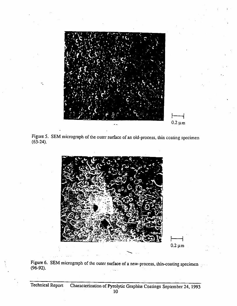
,
Figure 5 (63-24).
Figure 6. (96-92).
Technic;
t - .. 0.2 pm
. SEM micrograph of the outer surface of an old-process, thin coating specimen
H 0.2 pm
.\
SEM micrograph of the outer surface of a new-process, thin-coating specimen
Repon Characterization of Pyrolytic Graphite Coatings September 24. 1993 10

H 0.2 p m
Figure 7. SEM micrograph of the outer surface of a new-process, thick-coating specimen (89-44).
H 0.5 pm
Figure 8. SEM micrograph of a fractured cross section of an old-process, thin-coating specimen (63-24).
Technical Report Characterization of Pyrolytic Graphite Coatings September 24. 1993 11
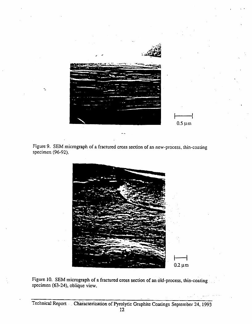
i =
H 0.5 pm
Figure 9. SEM micrograph of a fractured cross section of an new-process, thin-coating specimen (96-92).
Figure 10. SEM micrograph of a fractured cross section of an old-process, thin-coating specimen (63-24). oblique view.
Technical Repon Characterization of Pyrolytic Graphite Coatings September 24, 1993 12
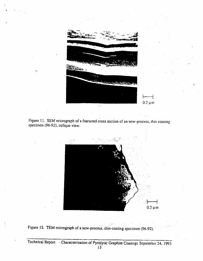
H 0.2 pm
.. .
Figure 1 1. SEM micrograph of a fractured cross section of an new-process. thin coating specimen (96-92). oblique view.
H 0.2 pm
Figure 12. TEM micrograph of a new-process, thin-coating specimen (96-92).
Technical Report Characterization of Pyrolytic Graphite Coatings September 24. 1993 13

Figure 13. TEM diffraction pattern from the specimen area shown in Figure 13. Arrow poinis io 004 diffraction ring.
H 0.2 pm
Figure 14. ‘ E M micrograph of an old-process, thin-coating specimen (63-24). Arrow points to grain features (“dark spots”). .
Technical Report Characterization of Pyrolytic Graphite Coatings September 24. 199.7 14

Figure 15. E M diffraction pattern from sample area shown in Figure 15. Arrow points to "granular" structure seen in 004 diffraction ring.
...
Technical Report Characterization of Pyrolytic Graphite Coatings September 24, 1993 15


PIR 1218 Appendix B
PROCESS SPECIFICATION
POR
PYROLYTIC CARBON
Wartin Marietta Astro Space P.O. Box 8555
Philadelphia, PA 19101

23021539 -23 May 1994
Revision
-
- REVISION LOG
This log identifies those portions of this specification which have besn revised since original iaeue. Revired ortione of each page, for the current revision only, are identifie B by marginal rtriping.
Paragr-sgh Number(e) Affected
Initial Iseue
R ~ V . Date Approval
ii

SECT I ON/ PARAGRAPH
-
1.0 1.1 1.2 2.0 2.1 2.2 3.0 3.1 3.2 3.3 3.4 3.5 4.0 4.1 4.1.1 4.2 ~.~ 4.3 4.4 4.5 5.0 6.0 6.1
10.0
2 3 0 2 15 3 9 23 May 1994
. _- TABLE OF CONTENTS
PAGE -
SCOPE 1 SCOPE 1 CLASSIFICATION 1 APPLICABLE DOCUMENTS 2 GOVERNMENT DOCUMENTS 2 NON-GOVERNMENT DOCUMENT5 2 REQUIREMENTS 3 EQUIPMENT 3 MATERIALS 3 REQUIRED PROCEDURES 3 RECOMMENDED PROCEDURES 6 CERTX F ICATI ON 6 QUALITY ASSURANCE PROVISIONS 7 RESPONSIBILITY FOR INSPECTION 7 PURCHASER 1 MONITORING PROCEDURES-EQUIP 7 MONITORING PROCEDURES-MTLS 7
7 7
CERTIFICATION TEST METHODS PREPARATION-FOR DELIVERY NOTES
i R -
INTENDED USE 8
APPENDICES
CRITICAL ITEM CHECK SHEET

,

23021539 23 May 1994
. _ 1.0 SCOPE
- 1.1 SCOPE
This specification describes the peocessing requirements for the Chemical-Vapor Dopositlon (CVD) of Pyrol tic Carbon (PC) onto
t h e pyrQlytiC csrbon coating. graphite subetratee for the purpose of anc Y osing the graphite within
1.2 CLASSIFICATION
The proceoe covered by thie specification s h a l l be classified as follows:
- Part Description
1 Pyrolytic carbon overcoating of QRAL graphite substrates by using the technique of Chemical Vapor Depogition.

23021539 23 m y 1994
2.0 APPLICABLE DOCUMENTS
2.1 GOVERNMENT DOCUHENTS:
The following documents of the issue in effect for the program on which this epeciiicstion is ueed, form 8 part of thie specification to the extent specified herein. In the event of conflict between the documents referencod herein and the contents of thin epecification, the Content6 of this specification shall be considered a superseding requirement.
STANDARDS;
Military
2.2 NON-GOVERNMBNT DOCUHENTS
The following documants of the issue in effect for the program on which this specification is used, form a part o f this specification to the extent specified herein. In the event of conflict between the documents referenced herein and the contents o f this specification, the contenta of t h i s specification nhall be considered a supereeding requirement.
6PECIFICATIONS MARTIN MARIETTA ASTRO SPACE
171A4190 Solvents, Cleaning, High Purity
- 2 -

23021539 2 3 Nay 1 9 9 4
3 . 0 REQUIREXENTS
3.1 EQUZPMENT
The fo l lowing equipment mgy-be r equ i r ed t o comply w i t h t h i s s p e c i f i c a t i o n . 3 . 1 . 1 Pre-cleaned c l o t h s and wipes. -.
3.1.2 F i x t u r e s f o r ho ld ing and a l i g n i n g p l a t fo rm,
3.1.3 Forceps - 3 . 1 . 4 Finger co t8 ( o p t i o n a l )
3 . 2 MATERIALS
3 . 2 . 1 Solven t s complying w i t h 171A4190
3.2.2 Methane, CP grade , 990 methane min.
3.2.3 Ethane, CP grade , 99% e thane m i n .
3.2.4 Hydrogen, U l t r a High P u r i t y , 9 9 . 9 9 9 % hydrogen m i n .
3 . 2 . 5 Helium, t e c h n i c a l grade
3.2.6 Nit rogen , t e c h n i c a l grade
3.3 REQUIRED PROC5DURES
3.3.1 Examine t h e Engineer ing T e s t T i c k e t ( E T ) t o ensure t h a t no e x c e p t i o n s o r r e v i s i o n s a r e t aken i n r e f e r e n c e t o t h i s s p e c i f i c a t i o n .
3.3,2 Wipe t h e p l a t fo rm w i t h a pre-cleaned c l o t h o r wipe t o remove any l o o a e p a r t i c u l a t e s . Pay s p e c i a l a t t e n t i d n t o any p o t e n t i a l l y l o o s e p y r o l y t i c carbon f r a y i n g s .
Load t h e p l a t f o r m ( s e e Figure 1 ) ' per t h e i n s t r u c t i o n s on t h e Engineer ing Tes t T i c k e t . CAUTION: ONLY handle t h e s u b s t r a t e s w i t h f i n g e r c o t s and /o r - so lven t c leaned fo rceps !
3.3.3
- 3 -

23021539 25 May 1994
., . . . .
LEVEL#
2
- 3
4
5
f 7.375 ----------.I
.375(5 PLS)
S.).
?IGURE 1
- 4 -

23021539 23 May 1994
3.3.4
3.3.5
3.3.6
3 . 3 . 7
3.3.8
3.3.9
3.3.10
3.3.11
3.3.12
3.3.13
3.3.14
3.3.15
., The loading pattah of the platform shall be documented as the platform is being loading with the eubstrates. The substrates shall be visually inspected and any discrepancies shall be noted.
Tha working area of the furnace must be free of particulates and the gas nozzle must be inspected for deterioration.
The operators shall complete the Critical Item Check Bheet (see Section 10) to enmure the furnace has been inspected prior to start-up. Each pyrolytic carbon run shall have an individual run folder established.
Load the platform into the furnace working area. Subatrates shall not be touched during this process. Seal furnace and complete Critical Item Check Sheet.
Heat the furnace to 114OOC at 'a rate o f 30O0C/hr max.
Stabilize the furnace temperature at 1140oC and then hold f o r 1/2 hour min.
Purge the hydrogen, methane, and ethane gas lines prior to opening the furnace manifold by pressurizing and evacuating the gas llnes three times.
The hydro en, methane and ethane gases shall enter the furnace, fn this order, with a respective gas flow ratio o f 1015:1 SCFH. Allow BUffiCient time ( 2 minute8 min) between the atart-up of each gas for proceas pressure atabiliaation.
Set the process pressure at 17" Hg by throttling down the vacuum pump and purging the vacuum pump with nitrogen.
The typical deposition time o f the process shall be 240 minutes 2 10 minutes unless etipulated otheswiee in the Engineering Test Ticket.
The process shall be shut down by closing the ethane, methane, and hydrogen gae lines in this respective order. .The operators shall maintain 8 five (5) minute interval between each respective gas line closing to allow for sufficient evacuation of that gas.
~
open the vacuum system fully. Wait 5 minutes min. for total furnace evacuation,
- 5 -

23021539 23 may 1994
3.3.16 Shut the furnace power supply off.
3.3.17 Backfill the furnace chamber with Helium at a rate of 5Omm Hg/min max. a . ,
3 . 3 . 1 8 Allow furnace to cool for 24 hours.
3.3.19 Open furnace, remove platform of substrates, and package into the supplied holding units. The substrates shall be visually fnsptcted and any discrepancies shall be noted. Parts shall be handled with solvent cleaned forcepr, and/or finger cote.
3.4 RECOMMENDED PROCEDURES
This section is not applicable to this specification.
3.5 CERTIPI CATION
3.5.1 'All processing s h a l l be performed by experienced operators ' of induction heating furnaces and CVD procedures.

23021539 23 May 1994
4.0 QUALITY A S S U W C E PROVIBXONB
4.1 RESPONSIBILXTY FOR INSPECTION
4.1.1 Purchaser.
The purchaser shall review and evaluate the vendor’s documentation to adequately asaure compliance and acceptability.
4.2 MONITORING PROCEDURES - EQUIPMENT Xnatruments and test equipment shall have their accuracy verified in accordance with MIL-6TD-45662.
4 . 3 MONITORING PROCEDURES - MATERIAL8 It shall be verified that all materials are within the requirements of their respective specifications.
4 . 4 CERTIFXCATION
All processing h a l l be performed by experienced operators who are approved by the program office for this process.
4.5 TEST METHODS
The processed substrates shall be returned and tested i n accordance to the instructions on the respective Engineering Test Ticket.
- 7 -
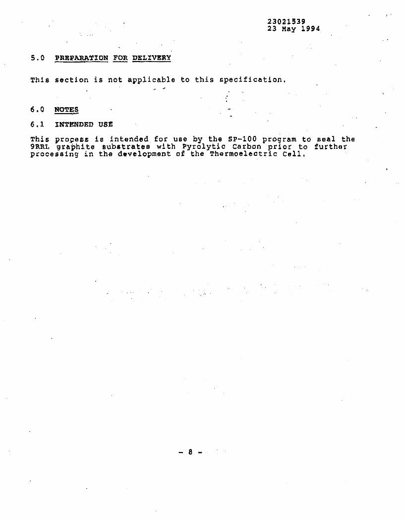
23021539 23 May 1994
5 . 0 PREPARATION FOR DESXVERY
This section is not applicable to this specification. > -
- 6 . 0 NOTES
6.1 INTENDED USE
This pro_cess is intended for u6e by the SP-100 pro ram to seal the
processing in the development o f the Thermoelectric Cell,
__c -
9RRL graphite substrates with Pyrolytic Carbon pr 9 o r to further
- a -

SECTION 10
APPENDIX
STEP NO. -
Martin Marietta
High Temperature Laboratory Instructions NO. 9133-938B-041 (Rev. 4 - 07/13/92)
CRITICAL ITEMS CHECX LIST FOR ALL INDUCTION FURNACE8
. - . Astro-Space
(To be s i g n e d off by Operator before each run) -
Date:
Run # a
CHECR ALL ITEMS AND CORRECT - I F Q D ~ ~ ~ E D O R E S T A R T - U P
CONDl TI ON
A. vacuum ~ u m g
3 . Oil level in pumps.
2 . Pro e r position of lubricating o i l valves. C3lf o n l y )
3. Cooling water to pump. (return h supply)
B. Vacuum Furnace
OPERATOR
1. Condition of temperature sight port. ( l f ~ l ' r i n g s f sight glassf sight valve and vent valve)
2. Visual check of coil cooling water hoses every run. Physical check every 10th run. Replace - hoses after 200 runs.
3. Furnace "0" r i n g s .
4. Cool ing water to lid (raturn and supply).

C . Induction Heater Con'ttol Cabinet
1. Cooling water t o : ( re turn & supply)
( a ) . Power supply c a b i n e t . (b). Induction c o i l .
2 . Proper p o s i t i o n of POWER I N P U ~ SELECTION SWITCH ( 3 0 0 O n l y ) _.
D . Syetem Evaluation
1-;
2 . Generator v o l t a g e control (Variac) a t z e r o ?
Take. leak ra te on complete vacuum system a f t e r three hours of t o t a l pumping t ime.
L
. . . ' . . , . . . . .

. Q . A . CHECK LIST
: = I / M Run # a f t e r last hose replacement . ’
I / M # of funs s i n c e replacement
* -
(1) f f more than 2 0 0 do not o p e r a t e furnace . -
I / N Run # which hoses were p h y s i c a l l y i n s p e c t e d and
I/M # of runs s i n c e l a s t p h y s i c a l i n s p e c t i o n and
accepted .
acceptance .
( 2 ) If more than 1 0 runs have been made Gince l a s t phye ica l i n s p e c t i o n do n o t o p e r a t e fu rnace .
I/M Run # which carbon b lack was l a s t changed.
I / M # of runs s i n c e carbon black was last changed.
( 3 ) I f more than 15 runs have been made s i n c e laBt carbon black change i n a 4 0 0 6e1-188, Do Not o p e r a t e fu rnace .
I f more than 4 5 runs have been made, i n 300 s e r i e s fu rnace a t l o w temp. (<llOO°C) s i n c e l a s t carbon b lack change, -- D o Not o p e r a t e fu rnace .

. i
f I ,
,

P PIR 1218 Appendix C
1.0 -:
This Specification defines the requirements for coatings of Si3N-i and Si02 on SPlOO TA Cell parts and assemblies.
!
rcnons DECIMALS ANGLES

. .
,_ ............ . . . . . . . . . . . ,. . ...
.. .
t
._... . . . . . I
__ I .. - . . ........... ,-, ,-,., . .,,
- , ,i
.. ,. . . . . . . . I_ . . . . . . . . ! ' . i
, ,. ,-
':.?(?Q6j52(? - <:\lP Si.?N4 and Si02 ,hating Service Specification
1.0 SCOI)E:
Psgo 2
This Specification defines the requirements for coatinss ci SisN4 and Si02 on SPlOO TA Cell parts and assemblies.
2 . 0 c $ -
The following documents form part-of this specification to the extent specified herein:
2 . 1 G p n p r n 1 m c t r i P riocuments: - ET3521 TA Electrode MoiGe Bond ET3522 TA Module Perimeter Glassed ET3523 TA Module Grooves Glassed ET3923 Transition Graphite Slice ET3925 Transition Electrode Hot Side Grooved ET3926 Trilnsition Electrode Cold Side Grooved ET3927 Hot Side Transition Electrode Grooves Glassed ET39 28 Cold Side Transition Electrode Grooves
ET39 34 Transition Sandwich Perimeter Glassed Glassed
'2.7 - t no,-- t .
Federal Standard 209E
:3. 0 _SEQUIREMENTS:
3.1 U P M F U T .
3.1.1 , The vendor s h a l l provide the equipment. as well as t h e related accessories and fixtures, to produce t.he coating .
:3.1.2 The vendor shall be responsible for maintaining the . . ep~ipment in nclminal operating conditions and for
calibration !~f critical parameters that is traceable t c NBS or Nationel Trade Association Standards:
The vendor shall 'train and,certify operators performing the deposition. . .
rJ. 5. Government personnel safety and Fnvironmental protection requirements. ' .
3.1.3
. . ... ) ." 3.1.4 The vendor shall operate in a manner that complies with
. . +
,. . . 3 . 2 MATERIAr,S: . . ;
The vendor shall provide all precursor materials with minimum purities that meet base level SEMI Standards, except as specified herein.
:3 .2 .1 99% minimum purity and specified for silicon ,nitride applikations. " .,

^ . ::.nt?fi52Q - O J D SiZN4 ani 2102 ??ge '3 .:.?at izg Service Specificstion
. ? . L . 2 a t i v e G w 99.9% minimum purity and ._. 17
specified f o r VLSJ semiconductor applications.
3 . 2 . 3 m-rei\Pt,ive I;-- -. 99.99% minimum purity 'and specified for VLSI semiconductor applications. -
'3 . :3 . 1 All specimen and surface preparation prior to deposition shall be the responsibility of General Electric.
The vendor may remove unattached particulate contamination by blowing with dry nitrogen ser: at delivery pressure of about 20 psig.
The vendor may perform additional surface preparation other than specified herein with prior written approval by General Electric.
.. ,-. ..)..3.2
- :? . .? . 4
The vendor shall demonstrate that the process selected produces deposits that meet the requirements specified herein on specimens to be provided by General Electric.
General Electric will evaluate the specimens coated by the vendor and make a determination if the costings meet the requirements specified herein.
The process selected shall not significantly CSUSP deterioration nf the components and interface bonds ~f the parts and assemblies.
Module assemblies, ET3522 and ET2523. may not be subjected to heating and cooling rates higher than 15"C/min, or be placed directly into an environment that is higher than 125'C from room temperature. Average heating and cooling rates less than 15 'Chin are acceptable; and, these may be achieved either by continuous automatically controlled manner Qr in discrete steps of 75'C every 5 minutes.
Any post-depcsition treatments performed by the vendor. 50 be approved by General Electric, to enable the deposits to satisfy %he requirements herPin, shall form part of the process selected.
3.5 3 n c ; $.
3.5.1 Hardware may m l y be uncovered in better than class 100,000 particulate conditions per Federsl Standard

‘19006520 - ‘ Y D Si3N4 and Si02 Psgo 4 Ccacing Ser-rice Specification
209B. Never uncover hardware when exhaust from pumps or vacuum cleaners are open to a common envirsnmenc.
3.5.2 Wear white, latex, or equivalent protection gloves approved for Class 100 operations per Federal Standard 209B when moving hardware. Latex or vinyl gloves are preferred because it can be washed with them on. Operator mask and head cover are recommended. -
3.5.3 Minimize movement of uncovered hardware. Never transport hardware outside of its container. Keep containers covered when hardware is not being worked on. Never talk while hardware is uncovered. -
3 . 5 . 4 Do not touch the hardware! Not even with gloves on Only freshly cleaned tools, such as tweezers arp permitted to contact the hardware.
3 . 5 . 5 Non-metallic tweezers with flat tips are preferred. Metallic tweezers with sharp-edged tips must be lined with polyethylene or equivalent non-metallic material.
3 . 5 . 6 Immediately before inserting hardware into the reactor. blow off loose particulates with dry nitrogen or FREON. Never use breath to blow on hardware.
3 . 5 . 7 When transporting hardware between vendor and GE. seal individual parts in polyethylene bags or heat sealed compartments. Label and maintain part idencity.
3 . 6 . 1 SizN4 coatings must be 1 to 2 ,um thick on 311 surfaces specified below.
3 . 6 . 2 Si02 coatings must be 0.5 to 1 .um thick on all surfaces specified below.
The specified surfaces to be coated are:
3.7.1 ET3522 - TA Module Perimeter Glassed: Perimeter surfaces(-B- and -C-) (ref: ET3521, prior assembly to ET3522 REV C ) .
3.7.2 ET3523 - TA Module Grooves Glassed: Bottom snd wall surfaces of grooves and all perimeter surfaces(-B- and -C-), when specified (ref: ET3522 REV C, prior assembly to ET3523).
3 . 7 . 3 ET3923 - Trensition Graphite Slice: Llnmarked lateral surface(-A-) (ref: ET3923).
3.7.4 ET3927 - Hot Side Transition Electrode Grooves Glassed: Bottom and wall surfaces of the qrooves (ref: ET3925. prior assembly to

'2.XI1652Q - 3 V D SioN4 and Si02 :'oacing Service Speciiicacion
Psge 5
ET39271 and perimeter surfaces, when specified (ref: ET3934).
3.7.5 ET3928 - Cold Side Transition Electrode Groove? Glassed: Bottom and wall surfaces of. the grobvGs (ref: ET3926, prior assembly to ET3928) and perimeter surfaces. when specified (ref: ET3934 ) .
3.7.6 ET3934 - Transition Sandwich Perimeter Glassed: Perimeter surfaces (ref: ET3934).
- Assembly sketches are provided in Appendix 10 for reference.
3.3 r 4
3.8.1 Foreign material content shall not exceed 500 ppm.
3.9.2 The bulk resistivity of the coatings shall exceed 104 n-cm at 1000°C.
:3.3.3 As-deposited coatings shall not be crazed in over 10% of the area.
: 3 . 9 . 3 The coatings singly or Si02 over SiaN4 shall withstand vacuum heat treatment at 1200°C for 4 hours without more than 2% of the area covered spalling or being uncovered. Postdeposition treatments may be parformed by the vendor to enable the coatings to survive this treatment with the approval of General Electric. Acceptance of the procedure is still subject 70 paragraph 3.3.3.
:3.9 i pmnns
:3.3.1 The vendor shall keep detailed permanent recoris of sll parameters of each run. Significant events prior and during each run shall be recorded and attested to by the operator. Significant events shall include equipment malfunction and maintenance, previous deposition performed on the equipment, and utiiity outages.
General Electric r-eserves the right to receive hard copies and or obtain direct access to the vendor's permanent rec,ords pertaining to the deposition runs.
The minimum information that must be provided to
. . . .
3.9.2
. .
:3.9.3 ~ General Electric with each run'are:
1 ) Base Pressure ' ' 2 ) Operating Pressure
3) Gas Flow rates 4) Power input (.for PECVD) 5) Operating Frequency ( f o r PECVD) 6 ) Operating,Temperatures (a copy of temperacure vs
time chart is preferred)

':nc?65ZO . - rVD Si3N4 and Si& ?.eating Service Specification
7 ) Equipment identification 8 ) Operator identification 9 ) Certificate of Compliance or Non-Compliance Report
. . 4.0 u t . v As e PI. DV 1s1Dn5: . . . . 4.1 Certlflcat e nf COmD
4.1.1 The vendor shail issue a Certificate of Compliance with each coating run that the coating process complied with a11 the requirements herein or others agreed to in writing between the vendor and General Electric. -
4 . 1 . 2 The vendor shall issue a Non-Compliance Report for circumstances that are outside the vendor-s control. General Electric reserves the right to reject the run based solely on non-compliance with the process requirements.
4 . 2
General Electric shall perform visual inspection of the parts. The same inspection may be performed by the vendor at his discretion, provided that reports of such inspection are provided to General Electric.
Inspect parts for continuity and integrity of the coatings. Uncovered or spalled areas not to exceed 2% of the total required area or .010 inch in any direction on required areas.
4.2.1
4 . 2 . 2 Inspect for attached foreign material. No attached forsign material allDwed.
4.2.3 General Electric may accept coatings based on visuai inspection; but reserves the right to reject coatings based on other subsequent tests specified herein to be performed at General Electric-s discretion.
4.2 P
General Electric shall provide at lsast two witness coupons that shall be coated in the same run as the assemblies for measurements of thicknesses and for thermal tests. The vendor may use other witness coupons subject to the approval of General Electric for process control.
4 . 3 Q&Pr T 9 -9
4.3.1 - 9 P
At least one witness coupon shall be glassed and fused with GS526 using established methods. The thickness of the coatings shall be determined by metallography.

4 . 3 . 3
4 . 3 . 4
At leas+, one witness coupon shall be subjected to better than lo-= Torr vacuum 1200°C treatment for 4 hours. exceed 2% of the coupon area and .I110 inch in any direction.
Loss of-surface coverage or spalling shall not.
.. ' t ' pptermination:
Metallographic sections in paragraph 4.3 shall be examined by Enerzy Dispersive Spectrum Analysis to determine nominal composition and foreign materials. &ctr $,-a1 -ltv . . Measuremenf:
I f the coating survives the thermal test of Paragraph 4.3.2, tungsten electrodes shall be sputtered on the coupon and resistivity measurements at 1000°C shall be performed.

'23r?O9570 - CVfl Si3N4 and Si02 aloating Service Specification
APPENDIX 10 - ASSEMBLY SKETCHES
. ..
I,
. . . ., . ,
.,., . .
... . . ~ . : .

I i t 1.066(REF) 3 I I i SQUAFIE
PART N3.
ET3923 TRANSITION GRAPHITE SUCE GLASSED
MATERIAL
+.0005 -Oo20 -.oooo
P1
P 2
P3
P4
I ' m: 1. DWG TERMS AND TOLERANCES PER s30009.
9RRL
G90
HLM85
TBD
2. MARK 'ET3923P-' PER 532534 CL.10.
3. CVD Si3N4 ON UNMARKED SIDE(-A-) PER TA388.2 TO 2pm (TYP). CVD Si02 PER TA388.4 TO l p m (TYP). GLASS OVER CVD-Si (-A-) PER PD2-40 TO .0020+.0005 i'; -.OD00 INCH USING ET4005 COMPOSITE GLASS INK. BURNOUT BINDER PER PD2-50 USING 450°C . 7.
MAXIMUM TEMPERATURE. 1.4
80 Ir)
'3
:* 1 - ..; 4. NO CRACKS IN THE GLASS OR UNCOVERED AREAS I.
ON SIDE -A-. NO FOREIGN MATERIAL ALLOWED.

NOTE#4
ET3934 TFW\ISITION GRAPHITE SANDWICH
PERIMETER GLASSED
DEFECT CRlTERlA .I
PER NOTE#4 APPUES BETWEEN DASHED UNES
tam: 1. DWG TERMS AND TOLERANCES PER S30009.
2. MARK "ET3934P-' PER S32534 CL.10. I +
3. CVD-Si3N4 PERIMETER SIDES PER TA388.2 TO 2pm (TYP). CVD Si02 PER TA388.4 TO lpm (TYP). GLASS FOUR PERIMETER SIDES PER PD2-40 TO .008*.001 INCH. EXCEPT USE 450°C MAXIMUM TEMPERATURE. FUSE GLASS PER TA372.
BINDER BURNOUT PER PD2-50
4. UNCOVERED GRAPHITE AND DEFECTS(VO1DS. CHIPS, PITS, OR CRACKS) IN AREA INDICATED NOT TO EXCEED .010 IN ANY DIRECTION. ALL DEFECTS OUTSIDE ARE ACCEPTABLE. NO FOREIGN MATERIAL ALLOWED

. - . 020(REF) I;" .. .
..-I.. .
I
I
.002(MIN) RADIUS
ET3925 TRWSKION ELECTRODE
HOT SIDE GROOVED
DEFECT CRKERIA PER NOTE#4 APPLIES B W E E N DASHED LINES I
I
j .-I
MATERIAL z :"'"-I: HLM85
TBD P4
NOTES: 1. DWG TERMS AND TOLERANCES PER S30009
2. MARK "ET3925P-" PER S32534 CL.10.
3. LAP EXCESS GLASS AT EDGES. GRIND -6- SURFACE. MACHINE FINISH WITH 600 GRIT. DICE GROOVES WITH ,016 KERF BLADE. GROOVE MUST CUT THE LATERAL GLASS.
4. DEFECTS(VOIDS, CHIPS, PITS, OR CRACKS) IN AREA INDICATED NOT TO EXCEED ,010 IN ANY DIRECTION.
IN ANY DIRECTION. ALL DEFECTS OUTSIDE ARE ACCEPTABLE. NO FOREIGN MATERIAL ALLOWED.
DEFECTS ON SURFACE -B- NOT TO EXCEED .004 INCH

! '. . . . .
'.; 8 PLS.> !. . .
.016 TYP .051+.005 4- .- . 0 0 0
'. .002 P I P (REF) -._ -... -..; . _. .002(MIN)
RADIUS
MATERIAL c I p1 I 9RRL I E'; HLM85
TBD P4
133rrs: 1. DWG TERMS AND TOLERANCES PER $30009.
2. MARK 'ET3926P-' PER S32534 CL.10.
3. LAP EXCESS GLASS AT EDGES. GRIND -0- SURFACE. MACHINE FINISH WITH 600 GRIT. DICE GROOVES WITH .016 KERF BLADE. GROOVE MUST CUT THE LATERAL GLASS. P
in 6 [Tf Z W
4. DEFECTS(V0IDS. CHIPS, PITS, OR CRACKS) IN AREA INDICATED NOT TO EXCEED .010 IN ANY DIRECTION.
IN ANY DIRECTION. ALL DEFECTS OUTSIDE ARE ACCEPTABLE. NO FOREIGN MATERIAL ALLOWED.
n DEFECTS ON SURFACE -0- NOT TO EXCEED ,004 INCH x
*- 13

.064i:.OO1 ,026 TYP 3.- ,036 TYP
-. -. . - n
\ . .- . ._ . . -. ._ . .
'. i .., 7 PLS.
ET3927 TRJWSITION ELECTRODE
HOT SIDE GLASSED ..; b j 0 I ; ) OJ .a
P. < 0 0 m
LI 1 Lo r' 'd 1.1 m 2 f l b
H l l u r . 3 0 0 . PI rt co
HLM85 P
P4 TBD
I
s 5 NOTES: 1. DWG TERMS BE.. AND TOLERANCES PER S30009. 3 N
2. MARK "ET3927P-' PER S32534 CL.10.
3. CVD-Si3N4 LATERAL SIDES PER TA388.2 TO 2pm (TYP). CVD Si02 PER TA388.4,TO ipn (TYP). GLASS -8- LATERAL SURFACE PER PD2-40 TO
EXCEPT USE 450°C MAXIMUM TEMPERATURE. .017t.O01 INCH. BINDER BURNOUT PER PD2-50
FUSE LATERAL GLASS PER PD2-76.
4. LAP EXCESS GLASS AT EDGES. GRIND PERIMETER SURFACES TO CLEAN. REMOVE ,001 INCH MAX.
SHOWS; THEN, REMOVE ,024 INCH OF GRAPHITE.
P w '0 lrl 2 0
x
0
GRIND -8- LATERAL SURFACES UNTIL GRAPHITE
GRIND -A- SURFACE TO DIMENSION. n
I - 5. DEFECTS(VOIDS, CHIPS, PITS, OR CRACKS) ON GLASS
SURFACES NOT TO EXCEED .010 IN ANY DIRECTION. .
I I, DEFECTS ON SURFACES -A- AND -6- NOT TO EXCEED ., ,004 INCH IN ANY DIRECTION. NO FOREIGN MATERIAL
ALLOWED.

ET3928
,. . . . . \ ,
r' WID r . 3 O n . P,
TBD P4
NOTES: * t c o 1. DWG TERMS AND TOLERANCES PER 530009. 3 N :&
2. MARK 'ET3928P-' PER S32534 CL.10. --- -_____ 3. CVD-Si3N4 LATERAL SIDES PER TA388.2 TO
2pm (TYP). CVD Si02 PER TA388.4 TO l p m (TYP). GLASS -B- LATERAL SURFACE *PER PD2-40 TO .017*.00l INCH.
FUSE LATERAL GLASS PER PD2-76.
BINDER BURNOUT ,PER PD2-50 EXCEPT USE 450°C MAXIMUM TEMPERATURE.
4. LAP EXCESS GLASS AT EDGES.'GRIND PERIMETER i , i SURFACES TO CLEAN. REMOVE ,001 INCH MAX.
SHOWS; THEN, REMOVE .024 INCH OF GRAPHITE.
~ . , ~ . , i : . . GRIND -B- LATERAL SURFACES UNTIL GRAPHITE.
GRIND -A- SURFACE TO DIMENSION. L r t z W H
~... ". . .. 5. DEFECTS(VOIDS, CHIPS, PITS, OR CRACKS) ON GLASS x SURFACES NOT TO EXCEED .010 IN ANY DIRECTION. DEFECTS ON SURFACES -A- AND -B- NOT TO EXCEED ,004 INCH IN ANY DIRECTION. NO FOREIGN MATERIAL
. .~ . ,
ALLOWED.

L

,016 (NOM)
ET3522 REV I:
.I
2. HA11 PKB S32534 CL. IO.
5 .
?= a a IT ) z n
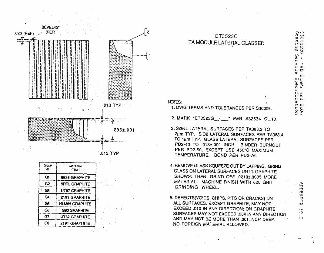
-- I r -
'a3MOllV lVltl3lVW N9l3kiO3 ON 'd330 H3NI 100' NVHI 3HOW 38 ION AVW aNV
3llHdVtl9 NO !N01133tlla ANV NI OLO' a333X3 ION AVW '3lIHdVtl3 ld33X3 'S33VjtlflS 11V
NO (SN3Vtl3 tl0 Slld 'SdlH3 'SalOA)Sl33j3a 'S
m
.-t
x ;;
~01133t~ia ANV NI POO. (3333x3 ION AVW s33vjtJns c
z u PI (Ir '133HM 9NlaNltl9 a: IltlE) 009 HllM HSlNl3 3NIH3VW 'lVltl31VW
3HOW SOOO'TOlZO' 330 aNltl9 'N3Hl :SMOHS 3lIHdVtlE) 1IlNfl S33VjtlflS lVH31M NO SSMC)
aNItlC) '9NlddV-l A8 1flO 3Z33flOS SSV-lnr3 3AOW3tl .V
'9L-lad tl3d aN08 '3tlfllVtl3dW31 WnWIXVW %OSV 3Sn ld33X3 'OS-lad H3d
tl3d S33VdtlnS 1Vtl31Vl SSW9 'dA1 UJdlO1 inown8 qziaNle 'H~NI ~OO~TE~O' 01 ov-zad
P'88EVl tl3d S33VJHnS lVtJ31M ZO!S 'dAl 01 Z'88EVl tl3d S33V3tlflS lVH31Vl PNE!S 'E
-- '01'13 PESZES tl3d . 9EZSE13. NtlVW '2
I I
dA1 €10'
100'?9 62'
.................... ............. \ ........ ;;<;;;?::?:?::::. ........ .. :... ....... ...................... ................. ...... ....._ ........... ...................... .................. ..... ........... .... ..._. ..... ....;..;. ................... I..>
................... ................. ..... .;... ..... ....... ....... ...... ..?..:. :..j..i.. __ i..i..i.
......... ..... ................. .:.>:.>. .:; .>. .>. .>. ._ i...
............. ....... ...................... :~,;:;..:;;:~~:..~:~~.~; ............... ....... ....... .............. i ..... ..:. :... ;...;...,;~;z.;...:;~~~~ ............... i .... ........................ ................. .i ...... i..:. . ..... .._: .... '.: .-..i;.:.,::) .. ..: .....
....... : x.>::..:<.::.
..2;::::::.:...:;:...>; i
...... 1 4 ----- ...... .:... .:;:: : :'. '-&-