phase-field models for simulating physical vapor
TRANSCRIPT
University of Arkansas, Fayetteville University of Arkansas, Fayetteville
ScholarWorks@UARK ScholarWorks@UARK
Graduate Theses and Dissertations
5-2016
Phase-Field Models for Simulating Physical Vapor Deposition and Phase-Field Models for Simulating Physical Vapor Deposition and
Microstructure Evolution of Thin Films Microstructure Evolution of Thin Films
James Stewart Jr. University of Arkansas, Fayetteville
Follow this and additional works at: https://scholarworks.uark.edu/etd
Part of the Nanoscience and Nanotechnology Commons, and the Structural Materials Commons
Citation Citation Stewart, J. (2016). Phase-Field Models for Simulating Physical Vapor Deposition and Microstructure Evolution of Thin Films. Graduate Theses and Dissertations Retrieved from https://scholarworks.uark.edu/etd/1481
This Dissertation is brought to you for free and open access by ScholarWorks@UARK. It has been accepted for inclusion in Graduate Theses and Dissertations by an authorized administrator of ScholarWorks@UARK. For more information, please contact [email protected].

Phase-Field Models for Simulating Physical Vapor Deposition
and Microstructure Evolution of Thin Films
A dissertation submitted in partial fulfillment
of the requirements for the degree of
Doctor of Philosophy in Microelectronics - Photonics
by
James A. Stewart, Jr.
Alfred University
Bachelor of Arts in Physics and Mathematics, 2009
University of Arkansas
Master of Science in Microelectronics - Photonics, 2012
May 2016
University of Arkansas
This dissertation is approved for recommendation to the Graduate Council.
Dr. Douglas E. Spearot Dr. Hameed A. Naseem
Dissertation Director Committee Member
Dr. Mark E. Arnold Dr. Rick L. Wise
Committee Member Committee Member
The following signatories attest that all software used in this dissertation was legally licensed for
use by James A. Stewart, Jr. for research purposes and publication.
James A. Stewart, Jr. Dr. Douglas E. Spearot
Student Dissertation Director
This dissertation was submitted to http://www.turnitin.com for plagiarism review by the TurnItIn
company’s software. The signatories have examined the report on this dissertation that was
returned by TurnItIn and attest that, in their opinion, the items highlighted by the software are
incidental to common usage and are not plagiarized material.
Dr. Rick L. Wise Dr. Douglas E. Spearot
Program Director Dissertation Director

Abstract
The focus of this research is to develop, implement, and utilize phase-field models to
study microstructure evolution in thin films during physical vapor deposition (PVD). There are
four main goals to this dissertation. First, a phase-field model is developed to simulate PVD of a
single-phase polycrystalline material by coupling previous modeling efforts on deposition of
single-phase materials and grain evolution in polycrystalline materials. Second, a phase-field
model is developed to simulate PVD of a polymorphic material by coupling previous modeling
efforts on PVD of a single-phase material, evolution in multiphase materials, and phase
nucleation. Third, a novel free energy functional is proposed that incorporates appropriate
energetics and dynamics for simultaneous modeling of PVD and grain evolution in single-phase
polycrystalline materials. Finally, these phase-field models are implemented into custom
simulation codes and utilized to illustrate these models’ capabilities in capturing PVD thin film
growth, grain and grain boundary (GB) evolution, phase evolution and nucleation, and
temperature evolution. In general, these simulations show: grain coarsening through grain
rotation and GB migration such that grains tend to align with the thin film surface features and
GBs migrate to locations between these features so that each surface feature has a distinct grain
and orientation; the incident vapor flux rate controls the density of the thin film and the
formation of surface and subsurface features; the substrate phase distribution initially acts as a
template for the growing microstructure until the thin film becomes sufficiently thick; latent heat
released during PVD increases the surface temperature of the thin film creating a temperature
gradient within the thin film influencing phase evolution and nucleation; and temperature
distributions lead to regions within the thin film that allow for multiple phases to be stable and

coexist. Further, this work shows the sequential approach for coupling phase-field models,
described in goals (i) and (ii) is sufficient to capture first-order features of the growth process,
such as the stagnation of GBs at the valleys of the surface roughness, but to capture higher-order
features, such as orientation gradients within columnar grains, the single free energy functional
approach developed in goal (iii) is necessary.

Acknowledgments
There are a number of people that I am very appreciative of for their contributions to me,
both personally and professionally, over the course of developing this research and dissertation.
First and foremost, I would like to thank my research advisor, Dr. Douglas E. Spearot, for giving
me the advice and freedom necessary to direct this research project in my own way, and his
guidance and support along the way in developing my ability to think creatively and
independently to become a better student and scientist. I would also like to thank all of my
colleagues in Dr. Spearot’s research group for numerous useful and entertaining discussions. I
am indebted to The University of Arkansas and the Microelectronics - Photonics (MicroEP)
Graduate Program for giving me the opportunity to continue my education with graduate studies
and to create my own M.S. and Ph.D. program in Applied Physics & Materials Science. Lastly, I
would like to thank the numerous family members and friends who supported me during the ups
and downs over the years and made life the most entertaining it could be outside of school. You
know who you are --- I love you.
This work was financially supported in part by the National Science Foundation under
Grant No. CMMI #0954505. The computational resources of this work are supported in part by
the National Science Foundation through grants MRI #0722625 (Star of Arkansas), MRI-R2
#0959124 (Razor), ARI #0963249 and #0918970 (CI-TRAIN), and a grant from the Arkansas
Science and Technology Authority, with resources managed by the Arkansas High Performance
Computing Center. Any opinions, findings and conclusions or recommendations expressed in
this material are those of the author and do not necessarily reflect the views of the National
Science Foundation.

Table of Contents
Chapter 1: Introduction . . . . . . . . . . . . . . . . . . . . . . . . . . . . . . . . . . . . . . . . . . . . . 1
1.1: Motivation for Scientific Research . . . . . . . . . . . . . . . . . . . . . . . . . . . . . . . . 1
1.2: Dissertation Objectives and Goals . . . . . . . . . . . . . . . . . . . . . . . . . . . . . . . . 6
1.3: Dissertation Structure . . . . . . . . . . . . . . . . . . . . . . . . . . . . . . . . . . . . . . . . 7
Chapter 2: Theory of Phase-Field Modeling and Simulation . . . . . . . . . . . . . . . . . . . . . . . 12
2.1: Introduction to Phase-Field Modeling . . . . . . . . . . . . . . . . . . . . . . . . . . . . . . 12
2.2: Physical Vapor Deposition . . . . . . . . . . . . . . . . . . . . . . . . . . . . . . . . . . . . . 16
2.3: Polycrystalline Materials . . . . . . . . . . . . . . . . . . . . . . . . . . . . . . . . . . . . . . 19
2.4: Materials with Multiple Solid Phases . . . . . . . . . . . . . . . . . . . . . . . . . . . . . . . 22
2.5: Phase Nucleation . . . . . . . . . . . . . . . . . . . . . . . . . . . . . . . . . . . . . . . . . . 26
Chapter 3: Formulation and Implementation of Phase-Field Models for Physical
Vapor Deposition and Microstructure Evolution . . . . . . . . . . . . . . . . . . . . . .
29
3.1: Introduction . . . . . . . . . . . . . . . . . . . . . . . . . . . . . . . . . . . . . . . . . . . . . 29
3.2: Physical Vapor Deposition and Polycrystalline Evolution . . . . . . . . . . . . . . . . . . . 30
3.3: Physical Vapor Deposition and Multiphase Evolution . . . . . . . . . . . . . . . . . . . . . 31
3.4: Enforcing the Multiphase Phase Fraction Interpretation . . . . . . . . . . . . . . . . . . . . 33
3.5: Numerical Solution Techniques . . . . . . . . . . . . . . . . . . . . . . . . . . . . . . . . . 35
3.5.1: Finite Difference Methods . . . . . . . . . . . . . . . . . . . . . . . . . . . . . . . . . . . . . 36
3.5.2: Method of Conjugate Gradients . . . . . . . . . . . . . . . . . . . . . . . . . . . . . . . . . . 40
Chapter 4: Phase-Field Simulations of Physical Vapor Deposition and
Microstructure Evolution of a Single-Phase Polycrystalline Metal . . . . . . . . . . . .
44
4.1: Introduction . . . . . . . . . . . . . . . . . . . . . . . . . . . . . . . . . . . . . . . . . . . . . 44

4.2: Simulation Methodology and Model Parameters . . . . . . . . . . . . . . . . . . . . . . . . 45
4.3: Substrates with Low-Angle and High-Angle Misorientations . . . . . . . . . . . . . . . . . 48
4.4: Effects of Varying Substrate Grain Sizes . . . . . . . . . . . . . . . . . . . . . . . . . . . . 51
4.5: Flux Rate Effects on Microstructure Evolution . . . . . . . . . . . . . . . . . . . . . . . . . 59
4.6: Summary and Concluding Remarks . . . . . . . . . . . . . . . . . . . . . . . . . . . . . . . 63
Chapter 5: Phase-Field Simulations of Physical Vapor Deposition and
Microstructure Evolution of a Two-Phase Metal . . . . . . . . . . . . . . . . . . . . . . .
66
5.1: Introduction . . . . . . . . . . . . . . . . . . . . . . . . . . . . . . . . . . . . . . . . . . . . . 66
5.2: Simulation Methodology and Model Parameters . . . . . . . . . . . . . . . . . . . . . . . . 67
5.3: Two-Dimensional Simulation Results and Discussion . . . . . . . . . . . . . . . . . . . . . 73
5.3.1: Low vs. High Interface Mobility Effects . . . . . . . . . . . . . . . . . . . . . . . . . . . . . . 73
5.3.2: Low Temperature PVD of a High Temperature Phase . . . . . . . . . . . . . . . . . . . . . 78
5.3.3: PVD on Substrates with a Temperature Distribution . . . . . . . . . . . . . . . . . . . . . . 80
5.4: Three-Dimensional Simulation Results and Discussion . . . . . . . . . . . . . . . . . . . . 83
5.5: Summary and Concluding Remarks . . . . . . . . . . . . . . . . . . . . . . . . . . . . . . . 85
Chapter 6: Extending a Free Energy Functional for Physical Vapor Deposition to
Include Single-Phase Polycrystalline Materials . . . . . . . . . . . . . . . . . . . . . . . .
88
6.1: Introduction . . . . . . . . . . . . . . . . . . . . . . . . . . . . . . . . . . . . . . . . . . . . . 88
6.2: Free Energy Functional and Equations of Motion . . . . . . . . . . . . . . . . . . . . . . . . 89
6.3: Simulation Methodology and Model Parameters . . . . . . . . . . . . . . . . . . . . . . . . 90
6.4: Substrate Grain Size and Vapor Flux Rate Effects . . . . . . . . . . . . . . . . . . . . . . . 93
6.5: Effects of Varying Grain Evolution Parameters 𝜏𝜃, 𝑠, and 휀 . . . . . . . . . . . . . . . . . . 100
6.6: Summary and Concluding Remarks . . . . . . . . . . . . . . . . . . . . . . . . . . . . . . . 108
Chapter 7: Conclusions and Recommendations . . . . . . . . . . . . . . . . . . . . . . . . . . . . . . . 111

7.1: Summary of Major Scientific Contributions . . . . . . . . . . . . . . . . . . . . . . . . . . . 111
7.2: Recommendations for Future Work . . . . . . . . . . . . . . . . . . . . . . . . . . . . . . . 115
References: . . . . . . . . . . . . . . . . . . . . . . . . . . . . . . . . . . . . . . . . . . . . . . . . . . . . . . 118
Appendix A: Description of Research for Popular Publication . . . . . . . . . . . . . . . . . . . . . . 123
Appendix B: Executive Summary of Newly Created Intellectual Property . . . . . . . . . . . . . . . . 127
Appendix C: Potential Patent and Commercialization Aspects of Listed Intellectual
Property . . . . . . . . . . . . . . . . . . . . . . . . . . . . . . . . . . . . . . . . . . . . . . . .
129
C.1: Patentability of Intellectual Property . . . . . . . . . . . . . . . . . . . . . . . . . . . . . . . 130
C.2: Commercialization Prospects . . . . . . . . . . . . . . . . . . . . . . . . . . . . . . . . . . . 130
C.3: Possible Prior Disclosure of Intellectual Property . . . . . . . . . . . . . . . . . . . . . . . 131
Appendix D: Broader Impacts of Research . . . . . . . . . . . . . . . . . . . . . . . . . . . . . . . . . . . 132
D.1: Applicability of Research Methods to Other Problems . . . . . . . . . . . . . . . . . . . . 133
D.2: Impact of Research Results on U.S. and Global Society . . . . . . . . . . . . . . . . . . . . 133
D.3: Impact of Research Results on the Environment . . . . . . . . . . . . . . . . . . . . . . . . 133
Appendix E: Microsoft Project for MicroEP PhD Degree Plan . . . . . . . . . . . . . . . . . . . . . . 134
Appendix F: Identification of All Software Used in Research and Dissertation
Generation . . . . . . . . . . . . . . . . . . . . . . . . . . . . . . . . . . . . . . . . . . . . . .
136
Appendix G: All Publications Published, Submitted and Planned . . . . . . . . . . . . . . . . . . . . . 138
List of Figures
Figure 1.1: Ti evaporated onto a steel substrate illustrating the influence of a
temperature gradient on phase and microstructure formation: A = large
columnar β-phase grains, B = coarse α-phase columnar structures, C = α-
phase whisker structures, D = fine α-phase columnar structures [9]. . . . . . . . . . . . . .
2
Figure 1.2:
Schematic representation of the PVD growth process. . . . . . . . . . . . . . . . . . . . . . .
3
Figure 1.3: (a) Schematic of a SZD showing each zone with their corresponding
physical processes and the influence of deposition conditions on the
microstructure, (b) Al sputtered onto a glass substrate within zone 1
(𝑇 𝑇m⁄ ~0.08), and (c) Zn evaporated onto a steel substrate within zone 2
(𝑇 𝑇m⁄ ~0.5) [6]. . . . . . . . . . . . . . . . . . . . . . . . . . . . . . . . . . . . . . . . . . . .
4
Figure 2.1: (a) Diffuse interface description, where the field variable varies
continuously between regions, and (b) Sharp interface description of
physical system [21]. . . . . . . . . . . . . . . . . . . . . . . . . . . . . . . . . . . . . . . . .
13
Figure 2.2: Schematic representation of a free energy density above, at, and below the
phase transition temperature for a solid-liquid system. The double-well
potential has minima at 𝜙 = 0 and 𝜙 = 1 corresponding to the stable
liquid and solid phases, respectively. . . . . . . . . . . . . . . . . . . . . . . . . . . . . . . .
15
Figure 2.3: Density profiles for simulated PVD illustrating the formation of surface
roughness, columnar structures, and porosity for a (a) vertical incident
vapor flux, (b) 45° off-axis incident vapor flux rate. (c) SEM of a Ge film
illustrating experimentally analogous structures [16]. . . . . . . . . . . . . . . . . . . . . . .
18
Figure 2.4: (Top) Evolution of a polycrystalline system with only a single solid phase
using the single-well potential, and (Bottom) evolution of a polycrystalline
system with both solid and liquid phases using the double-well potential.
Colors represent different grain orientations [23]. . . . . . . . . . . . . . . . . . . . . . . . .
22
Figure 2.5: Simulation results of isothermal solidification and impingement of four
isotropic solid particles with two different phases (red and yellow) in an
undercooled liquid (blue) via the multiphase phase-model with toy
parameters. . . . . . . . . . . . . . . . . . . . . . . . . . . . . . . . . . . . . . . . . . . . . . .
25
Figure 2.6: Simulated isothermal phase nucleation events and concurrent growth
within the microstructure of a binary metallic alloy [26]. . . . . . . . . . . . . . . . . . . . .
27

Figure 3.1: Code for the algorithms developed in this research for: (a) enforcing the
phase fraction condition in Equation 2.12, and (b) enforcing the phase
fraction conditions in Equations 3.1 and 2.12 to allow coupling of the
PVD and multiphase phase-field models as described in Section 3.3. . . . . . . . . . . . .
34
Figure 4.1: Grain evolution ( 𝜃 field) during simulated PVD on a polycrystalline
substrate with a single-well potential, low-angle GB misorientations, and
50 nm grains at time steps = 0 (a), 2500 (b), 5000 (c), 10000 (d). The 𝜃
field is plotted for regions where 𝑓 ≥ 0.5. The color legend shows grain
orientation in degrees relative to positive x-axis. . . . . . . . . . . . . . . . . . . . . . . . .
49
Figure 4.2: Grain evolution ( 𝜃 field) during simulated PVD on a polycrystalline
substrate with a double-well potential, low-angle GB misorientations, and
50 nm grains at time steps = 0 (a), 2500 (b), 5000 (c), 10000 (d). The 𝜃
field is plotted for regions where 𝑓 ≥ 0.5. The color legend shows grain
orientation in degrees relative to positive x-axis. . . . . . . . . . . . . . . . . . . . . . . . .
49
Figure 4.3: Grain evolution ( 𝜃 field) during simulated PVD on a polycrystalline
substrate with a single-well potential, high-angle GB misorientations, and
50 nm grains at time steps = 0 (a), 2500 (b), 5000 (c), 10000 (d). The 𝜃
field is plotted for regions where 𝑓 ≥ 0.5. The color legend shows grain
orientation in degrees relative to positive x-axis. . . . . . . . . . . . . . . . . . . . . . . . .
50
Figure 4.4: Grain evolution ( 𝜃 field) during simulated PVD on a polycrystalline
substrate with a double-well potential, high-angle GB misorientations, and
50 nm grains at time steps = 0 (a), 2500 (b), 5000 (c), 10000 (d). The 𝜃
field is plotted for regions where 𝑓 ≥ 0.5. The color legend shows grain
orientation in degrees relative to positive x-axis. . . . . . . . . . . . . . . . . . . . . . . . .
50
Figure 4.5: Grain evolution ( 𝜃 field) during simulated PVD on an amorphous
substrate (random grain orientations) with a single-well potential at time
steps = 0 (a), 2500 (b), 5000 (c), 10000 (d). The 𝜃 field is plotted for
regions where 𝑓 ≥ 0.5 . The color legend shows grain orientation in
degrees relative to positive x-axis. . . . . . . . . . . . . . . . . . . . . . . . . . . . . . . . . .
52
Figure 4.6: Grain evolution ( 𝜃 field) during simulated PVD on an amorphous
substrate (random grain orientations) with a double-well potential at time
steps = 0 (a), 2500 (b), 5000 (c), 10000 (d). The 𝜃 field is plotted for
regions where 𝑓 ≥ 0.5 . The color legend shows grain orientation in
degrees relative to positive x-axis. . . . . . . . . . . . . . . . . . . . . . . . . . . . . . . . . .
52
Figure 4.7: Grain evolution ( 𝜃 field) during simulated PVD on a polycrystalline
substrate with a single-well potential, high-angle GB misorientations, and
25 nm grains at time steps = 0 (a), 2500 (b), 5000 (c), 10000 (d). The 𝜃
field is plotted for regions where 𝑓 ≥ 0.5. The color legend shows grain
orientation in degrees relative to positive x-axis. . . . . . . . . . . . . . . . . . . . . . . . .
53

Figure 4.8:
Grain evolution ( 𝜃 field) during simulated PVD on a polycrystalline
substrate with a double-well potential, high-angle GB misorientations, and
25 nm grains at time steps = 0 (a), 2500 (b), 5000 (c), 10000 (d). The 𝜃
field is plotted for regions where 𝑓 ≥ 0.5. The color legend shows grain
orientation in degrees relative to positive x-axis. . . . . . . . . . . . . . . . . . . . . . . . . .
53
Figure 4.9: Grain evolution ( 𝜃 field) during simulated PVD on a polycrystalline
substrate with a single-well potential, high-angle GB misorientations, and
100 nm grains at time steps = 0 (a), 2500 (b), 5000 (c), 10000 (d). The 𝜃
field is plotted for regions where 𝑓 ≥ 0.5. The color legend shows grain
orientation in degrees relative to positive x-axis. . . . . . . . . . . . . . . . . . . . . . . . .
55
Figure 4.10: Grain evolution ( 𝜃 field) during simulated PVD on a polycrystalline
substrate with a double-well potential, high-angle GB misorientations, and
100 nm grains at time steps = 0 (a), 2500 (b), 5000 (c), 10000 (d). The 𝜃
field is plotted for regions where 𝑓 ≥ 0.5. The color legend shows grain
orientation in degrees relative to positive x-axis. . . . . . . . . . . . . . . . . . . . . . . . .
55
Figure 4.11: Grain evolution ( 𝜃 field) during simulated PVD on a polycrystalline
substrate with a single-well potential, high-angle GB misorientations, and
166.6 nm grains at time steps = 0 (a), 2500 (b), 5000 (c), 10000 (d). The 𝜃
field is plotted for regions where 𝑓 ≥ 0.5. The color legend shows grain
orientation in degrees relative to positive x-axis. . . . . . . . . . . . . . . . . . . . . . . . .
57
Figure 4.12: Grain evolution ( 𝜃 field) during simulated PVD on a polycrystalline
substrate with a double-well potential, high-angle GB misorientations, and
166.6 nm grains at time steps = 0 (a), 2500 (b), 5000 (c), 10000 (d). The 𝜃
field is plotted for regions where 𝑓 ≥ 0.5. The color legend shows grain
orientation in degrees relative to positive x-axis. . . . . . . . . . . . . . . . . . . . . . . . .
57
Figure 4.13: Phase (top) and grain (bottom) evolution during simulated low flux-rate
PVD with a single-well potential, high-angle GB misorientations, and 50
nm grains at time steps = 10 (a) & (c), and 35000 (b) & (d). The top color
legend indicates local density while the bottom legend shows grain
orientation in degrees relative to the positive x-axis. . . . . . . . . . . . . . . . . . . . . . . .
60
Figure 4.14: Phase (top) and grain (bottom) evolution during simulated low flux-rate
PVD with a double-well potential, high-angle GB misorientations, and 50
nm grains at time steps = 10 (a) & (c), and 35000 (b) & (d). The top color
legend indicates local density while the bottom legend shows grain
orientation in degrees relative to the positive x-axis. . . . . . . . . . . . . . . . . . . . . . . .
60
Figure 4.15: Phase (top) and grain (bottom) evolution during simulated high flux-rate
PVD with a single-well potential, high-angle GB misorientations, and 50
nm grains at time steps = 1000 (a) & (c), and 5500 (b) & (d). The top color
legend indicates local solid density while the bottom legend shows grain
orientation in degrees relative to the positive x-axis. . . . . . . . . . . . . . . . . . . . . . . .
62

Figure 4.16: Phase (top) and grain (bottom) evolution during simulated high flux-rate
PVD with a double-well potential, high-angle GB misorientations, and 50
nm grains at time steps = 1000 (a) & (c), and 5500 (b) & (d). The top color
legend indicates local solid density while the bottom legend shows grain
orientation in degrees relative to the positive x-axis. . . . . . . . . . . . . . . . . . . . . . . .
62
Figure 5.1:
Test PVD simulations for varying domain sizes illustrating the average
temperature value and evolution at y = 100. . . . . . . . . . . . . . . . . . . . . . . . . . . . .
68
Figure 5.2: Nucleation probability profiles using Equation 5.1 and the physical
parameters and relationships motivated by two-phase Ti. . . . . . . . . . . . . . . . . . . .
72
Figure 5.3:
Simulated PVD on an amorphous substrate with 𝜇 = 0.0035 cm s ∙ K⁄ ,
𝑇 = 1350 K and 𝛽∗ = 0.25 ∙ 10−35at time steps (a) 0, (b) 2500000, (c)
6250000, and (d) 12500000. The phase with the maximum local volume
fraction is plotted. (e) Global volume fraction evolution of each phase
during the PVD simulation. The constant volume fraction of the substrate
is included in this calculation to provide a consistent description with the
images on the left. . . . . . . . . . . . . . . . . . . . . . . . . . . . . . . . . . . . . . . . . . . .
74
Figure 5.4:
Simulated PVD on a bicrystal substrate with 𝜇 = 0.0035 cm s ∙ K⁄ , 𝑇 =1350 K and 𝛽∗ = 0.25 ∙ 10−35 at time steps (a) 0, (b) 2500000, (c)
7500000, and (d) 12500000. The phase with the maximum local volume
fraction is plotted. (e) Global volume fraction evolution of each phase
during the PVD simulation. The constant volume fraction of the substrate
is included in this calculation to provide a consistent description with the
images on the left. . . . . . . . . . . . . . . . . . . . . . . . . . . . . . . . . . . . . . . . . . . .
74
Figure 5.5:
Simulated PVD on an amorphous substrate with 𝜇 = 0.035 cm s ∙ K⁄ , 𝑇 =1350 K and 𝛽∗ = 0.25 ∙ 10−35 at time steps (a) 0, (b) 2500000, (c)
6250000, and (d) 12500000. The phase with the maximum local volume
fraction is plotted. (e) Global volume fraction evolution of each phase
during the PVD simulation. The constant volume fraction of the substrate
is included in this calculation to provide a consistent description with the
images on the left. . . . . . . . . . . . . . . . . . . . . . . . . . . . . . . . . . . . . . . . . . . .
76
Figure 5.6:
Simulated PVD on a bicrystal substrate with 𝜇 = 0.035 cm s ∙ K⁄ , 𝑇 =1350 K and 𝛽∗ = 0.25 ∙ 10−35 at time steps (a) 0, (b) 2500000, (c)
7500000, and (d) 12500000. The phase with the maximum local volume
fraction is plotted. (e) Global volume fraction evolution of each phase
during the PVD simulation. The constant volume fraction of the substrate
is included in this calculation to provide a consistent description with the
images on the left. . . . . . . . . . . . . . . . . . . . . . . . . . . . . . . . . . . . . . . . . . . .
76

Figure 5.7:
Simulated PVD on a 𝛽 -phase substrate with 𝜇 = 0.035 cm s ∙ K⁄ , 𝑇 =900 K and 𝛽∗ = 0.25 ∙ 10−35 at time steps (a) 0, (b) 3750000, (c)
7500000, and (d) 12500000. The phase with the maximum local volume
fraction is plotted. (e) Global volume fraction evolution of each phase
during the PVD simulation. The constant volume fraction of the substrate
is included in this calculation to provide a consistent description with the
images on the left. . . . . . . . . . . . . . . . . . . . . . . . . . . . . . . . . . . . . . . . . . . .
79
Figure 5.8:
Simulated PVD on a 𝛽 -phase substrate with 𝜇 = 0.035 cm s ∙ K⁄ , 𝑇 =1080 K and 𝛽∗ = 0.25 ∙ 10−35 at time steps (a) 0, (b) 3750000, (c)
7500000, and (d) 12500000. The phase with the maximum local volume
fraction is plotted. (e) Global volume fraction evolution of each phase
during the PVD simulation. The constant volume fraction of the substrate
is included in this calculation to provide a consistent description with the
images on the left. . . . . . . . . . . . . . . . . . . . . . . . . . . . . . . . . . . . . . . . . . . .
79
Figure 5.9:
Simulated PVD on an amorphous substrate with 𝜇 = 0.035 cm s ∙ K⁄ ,
𝛽∗ = 0.25 ∙ 10−35 and a temperature distribution that follows a Gaussian
profile with 𝑇 = 1350 K in the middle of the system and 𝑇 = 1000 K at
the horizontal boundaries at time steps (a) 0, (b) 2500000, (c) 7500000,
and (d) 12500000. The phase with the maximum local volume fraction is
plotted. (e) Global volume fraction evolution of each phase during the
PVD simulation. The constant volume fraction of the substrate is included
in this calculation to provide a consistent description with the images on
the left. . . . . . . . . . . . . . . . . . . . . . . . . . . . . . . . . . . . . . . . . . . . . . . . . .
81
Figure 5.10:
Simulated PVD on a bicrystal substrate with 𝜇 = 0.035 cm s ∙ K⁄ , 𝛽∗ =0.25 ∙ 10−35 and a temperature distribution that follows a Gaussian profile
with 𝑇 = 1350 K at the middle of the system and 𝑇 = 1000 K at the
horizontal boundaries at time steps (a) 0, (b) 2500000, (c) 7500000, and
(d) 12500000. The phase with the maximum local volume fraction is
plotted. (e) Global volume fraction evolution of each phase during the
PVD simulation. The constant volume fraction of the substrate is included
in this calculation to provide a consistent description with the images on
the left. . . . . . . . . . . . . . . . . . . . . . . . . . . . . . . . . . . . . . . . . . . . . . . . . .
81
Figure 5.11:
Simulated PVD on bicrystal substrate with 𝐴𝑦 = −0.6 , 𝜇 =
0.035 cm s ∙ K⁄ and 𝑇 = 1350 K at time step 107 where (a) is the phase-
field, (b) is the underlying multiphase field, and (c) is the temperature
field. All data is plotted for regions where 𝑓 ≥ 0.5. . . . . . . . . . . . . . . . . . . . . . . .
84
Figure 5.12:
Simulated PVD on a bicrystal substrate with 𝐴𝑦 = −2.5 , 𝜇 =
0.035 cm s ∙ K⁄ and 𝑇 = 1350 K at time step 5 ∙ 106 where (a) is the
phase-field, (b) is the underlying multiphase field, and (c) is the
temperature field All data is plotted for regions where 𝑓 ≥ 0.5. . . . . . . . . . . . . . . . .
84
Figure 6.1:
Grain evolution ( 𝜃 field) during simulated PVD on a polycrystalline
substrate with low-angle GB misorientations and 50 nm grains at time
steps = 0 (a), 2500 (b), 5000 (c), 10000 (d). The 𝜃 field is plotted for
regions where 𝑓 ≥ 0.5 . The color legend shows grain orientation in
degrees relative to positive x-axis. . . . . . . . . . . . . . . . . . . . . . . . . . . . . . . . . .
94
Figure 6.2:
Grain evolution ( 𝜃 field) during simulated PVD on a polycrystalline
substrate with high-angle GB misorientations and 50 nm grains at time
steps = 0 (a), 2500 (b), 5000 (c), 10000 (d). The 𝜃 field is plotted for
regions where 𝑓 ≥ 0.5 . The color legend shows grain orientation in
degrees relative to positive x-axis. . . . . . . . . . . . . . . . . . . . . . . . . . . . . . . . . .
94
Figure 6.3:
Grain evolution ( 𝜃 field) during simulated PVD on an amorphous
substrate (random grain orientations) at time steps = 0 (a), 2500 (b), 5000
(c), 10000 (d). The 𝜃 field is plotted for regions where 𝑓 ≥ 0.5. The color
legend shows grain orientation in degrees relative to positive x-axis. . . . . . . . . . . . . .
96
Figure 6.4:
Grain evolution ( 𝜃 field) during simulated PVD on a polycrystalline
substrate with high-angle GB misorientations and 25 nm grains at time
steps = 0 (a), 2500 (b), 5000 (c), 10000 (d). The 𝜃 field is plotted for
regions where 𝑓 ≥ 0.5 . The color legend shows grain orientation in
degrees relative to positive x-axis. . . . . . . . . . . . . . . . . . . . . . . . . . . . . . . . . .
65
Figure 6.5:
Grain evolution ( 𝜃 field) during simulated PVD on a polycrystalline
substrate with high-angle GB misorientations and 100 nm grains at time
steps = 0 (a), 2500 (b), 5000 (c), 10000 (d). The 𝜃 field is plotted for
regions where 𝑓 ≥ 0.5 . The color legend shows grain orientation in
degrees relative to positive x-axis. . . . . . . . . . . . . . . . . . . . . . . . . . . . . . . . . .
97
Figure 6.6:
Grain evolution ( 𝜃 field) during simulated PVD on a polycrystalline
substrate with high-angle GB misorientations and 166.6 nm grains at time
steps = 0 (a), 2500 (b), 5000 (c), 10000 (d). The 𝜃 field is plotted for
regions where 𝑓 ≥ 0.5 . The color legend shows grain orientation in
degrees relative to positive x-axis. . . . . . . . . . . . . . . . . . . . . . . . . . . . . . . . . .
97
Figure 6.7:
Phase (top) and grain (bottom) evolution during simulated low flux-rate
PVD with high-angle GB misorientations and 50 nm grains at time steps =
1000 (a) & (c), and 34000 (b) & (d). The top color legend indicates local
density while the bottom legend shows grain orientation in degrees
relative to the positive x-axis. . . . . . . . . . . . . . . . . . . . . . . . . . . . . . . . . . . . .
99
Figure 6.8:
Phase (top) and grain (bottom) evolution during simulated high flux-rate
PVD with high-angle GB misorientations and 50 nm grains at time steps =
1000 (a) & (c), and 5500 (b) & (d). The top color legend indicates local
solid density while the bottom legend shows grain orientation in degrees
relative to the positive x-axis. . . . . . . . . . . . . . . . . . . . . . . . . . . . . . . . . . . . .
99

Figure 6.9:
Grain evolution ( 𝜃 field) during simulated PVD on a polycrystalline
substrate with high-angle GB misorientations, 50 nm grains, 𝜏𝜃 = 100 ,
𝑠 = 0.01, and 휀 = 0.005 at time steps = 0 (a), 2500 (b), 5000 (c), 10000
(d). The 𝜃 field is plotted for regions where 𝑓 ≥ 0.5. The color legend
shows grain orientation in degrees relative to positive x-axis. . . . . . . . . . . . . . . . . .
101
Figure 6.10:
Grain evolution ( 𝜃 field) during simulated PVD on a polycrystalline
substrate with high-angle GB misorientations, 50 nm grains, 𝜏𝜃 = 10−1,
𝑠 = 0.01, and 휀 = 0.005 at time steps = 0 (a), 2500 (b), 5000 (c), 10000
(d). The 𝜃 field is plotted for regions where 𝑓 ≥ 0.5. The color legend
shows grain orientation in degrees relative to positive x-axis. . . . . . . . . . . . . . . . . .
102
Figure 6.11:
Grain evolution ( 𝜃 field) during simulated PVD on a polycrystalline
substrate with high-angle GB misorientations, 50 nm grains, 𝜏𝜃 = 10−1,
𝑠 = 0.1, and 휀 = 0.005 at time steps = 0 (a), 2500 (b), 5000 (c), 10000
(d). The 𝜃 field is plotted for regions where 𝑓 ≥ 0.5. The color legend
shows grain orientation in degrees relative to positive x-axis. . . . . . . . . . . . . . . . . .
102
Figure 6.12: Grain evolution ( 𝜃 field) during simulated PVD on a polycrystalline
substrate with high-angle GB misorientations, 50 nm grains, 𝜏𝜃 = 10−1,
𝑠 = 0.01, and 휀 = 0.05 at time steps = 0 (a), 2500 (b), 5000 (c), 10000
(d). The 𝜃 field is plotted for regions where 𝑓 ≥ 0.5. The color legend
shows grain orientation in degrees relative to positive x-axis. . . . . . . . . . . . . . . . . .
103
Figure 6.13: Grain evolution ( 𝜃 field) during simulated PVD on a polycrystalline
substrate with high-angle GB misorientations, 50 nm grains, 𝜏𝜃 = 10−1,
𝑠 = 0.1, and 휀 = 0.05 at time steps = 0 (a), 2500 (b), 5000 (c), 10000 (d).
The 𝜃 field is plotted for regions where 𝑓 ≥ 0.5. The color legend shows
grain orientation in degrees relative to positive x-axis. . . . . . . . . . . . . . . . . . . . . .
103
Figure 6.14: Grain evolution ( 𝜃 field) during simulated PVD on a polycrystalline
substrate with high-angle GB misorientations, 50 nm grains, 𝜏𝜃 = 10−2,
𝑠 = 0.01, and 휀 = 0.005 at time steps = 0 (a), 2500 (b), 5000 (c), 10000
(d). The 𝜃 field is plotted for regions where 𝑓 ≥ 0.5. The color legend
shows grain orientation in degrees relative to positive x-axis. . . . . . . . . . . . . . . . . .
105
Figure 6.15: Grain evolution ( 𝜃 field) during simulated PVD on a polycrystalline
substrate with high-angle GB misorientations, 50 nm grains, 𝜏𝜃 = 10−2,
𝑠 = 0.1, and 휀 = 0.005 at time steps = 0 (a), 2500 (b), 5000 (c), 10000
(d). The 𝜃 field is plotted for regions where 𝑓 ≥ 0.5. The color legend
shows grain orientation in degrees relative to positive x-axis. . . . . . . . . . . . . . . . . .
105

Figure 6.16: Grain evolution ( 𝜃 field) during simulated PVD on a polycrystalline
substrate with high-angle GB misorientations, 50 nm grains, 𝜏𝜃 = 10−2,
𝑠 = 0.01, and 휀 = 0.05 at time steps = 0 (a), 2500 (b), 5000 (c), 10000
(d). The 𝜃 field is plotted for regions where 𝑓 ≥ 0.5. The color legend
shows grain orientation in degrees relative to positive x-axis. . . . . . . . . . . . . . . . . .
106
Figure 6.17: Grain evolution ( 𝜃 field) during simulated PVD on a polycrystalline
substrate with high-angle GB misorientations, 50 nm grains, 𝜏𝜃 = 10−2,
𝑠 = 0.1, and 휀 = 0.05 at time steps = 0 (a), 2500 (b), 5000 (c), 10000 (d).
The 𝜃 field is plotted for regions where 𝑓 ≥ 0.5. The color legend shows
grain orientation in degrees relative to positive x-axis. . . . . . . . . . . . . . . . . . . . . .
106

List of Tables
Table 4.1:
Non-dimensional parameters used to simulate columnar and porous
growth during purely vertical PVD. . . . . . . . . . . . . . . . . . . . . . . . . . . . . . . . .
46
Table 5.1:
Non-dimensional parameters used to simulate columnar and porous
growth during purely vertical PVD. . . . . . . . . . . . . . . . . . . . . . . . . . . . . . . . .
69
Table 5.2: Physical parameters for a two-phase metallic system used to simulate
multiphase evolution during PVD. . . . . . . . . . . . . . . . . . . . . . . . . . . . . . . . . .
70
Table 6.1: Non-dimensional parameters used to simulate columnar and porous
growth during purely vertical PVD. . . . . . . . . . . . . . . . . . . . . . . . . . . . . . . . .
92

1
Chapter 1: Introduction
1.1 Motivation for Scientific Research
Over the last several decades, thin films have been the focus of considerable research due
to their variety of applications in optoelectronic and microelectronic devices, in
nanoelectromechanical systems, as protective coatings, etc. [1]. Thin films are usually grown
using physical vapor deposition (PVD) or chemical vapor deposition (CVD) techniques, where
the precise deposition conditions and materials used strongly influence the surface morphology
and underlying microstructure (e.g., phase formation, phase distribution, grain size, grain
orientation, etc.) that arises during processing [1-8]. For example, Figure 1.1 illustrates the
presence of a temperature gradient causing the formation of stable α and β Ti phases during
high-rate PVD, with varying microstructures in the α-phase regions [9]. The thickness of a thin
film, surface features, and underlying microstructure features are usually in the nano to

2
microscale range. Furthermore, the underlying microstructure may be amorphous or consist of
domains that differ in phase, i.e. crystal structure, grain orientation, and/or chemical
composition. The exact details of these surface and subsurface features greatly influence the
mechanical and electrical properties of the thin film, thus dictating the usefulness of the thin film
for a specific application [1-8,10,11]. During the deposition of some materials, multiple stable or
metastable phases may nucleate and coarsen that will either enhance or diminish the desired thin
film properties [11-15]. Therefore, to properly investigate and understand the connection
between thin film properties and vapor deposition conditions, it is crucial to consider several
physical processes including the vapor deposition technique used and both the formation of
phases, grains, and grain boundaries, and the interaction and evolution of these entities during
vapor deposition.
Figure 1.1: Ti evaporated onto a steel substrate illustrating the influence of a temperature
gradient on phase and microstructure formation: A = large columnar β-phase grains, B = coarse
α-phase columnar structures, C = α-phase whisker structures, D = fine α-phase columnar
structures [9].

3
This research focused specifically on the PVD process, shown schematically in Figure
1.2. PVD is a vapor deposition technique in which atoms are evaporated or sputtered from a
target material source. These ejected atoms then travel through the deposition chamber and
condense into a solid as a coating on a substrate. The PVD process is performed in a vacuum or a
very low-pressure environment with an inert or active atmosphere (i.e., an Al vapor phase could
react with an O atmosphere to produce the compound, e.g., Al2O3). The low pressures used in
PVD significantly reduce the number of gas-phase reactions and collisions during vapor
transport, thus allowing physical processes to dominate [5,6]. With these aspects in mind, this
research focused on the PVD growth process to provide simplicity in developing a physical
model because (i) the composition of the ejected target material is conserved during transport to
the deposition surface and (ii) chemical reactions and composition changes can be neglected due
to the vacuum or low-pressure environment (provided the thin film material is composed of a
single element or a compound where all phases have the same stoichiometry, e.g., Al2O3).
Figure 1.2: Schematic representation of the PVD growth process.
4
During PVD, incident atoms may not impinge on the substrate or growing thin film surface in a
spatially and temporally uniform manner with little adatom rearrangement, thereby creating
fluctuations that give rise to surface roughness. These fluctuations compete with surface
diffusion, which attempts to smooth the surface, resulting in nano to microscale surface features.
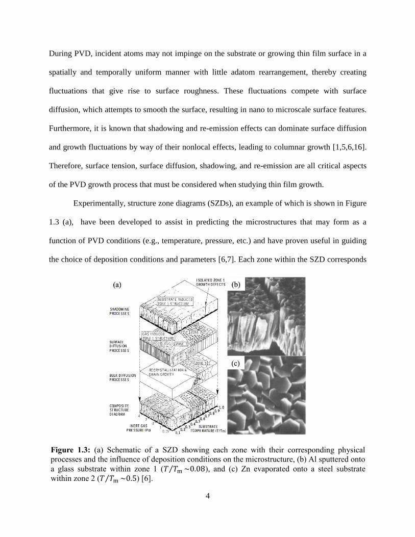
Furthermore, it is known that shadowing and re-emission effects can dominate surface diffusion
and growth fluctuations by way of their nonlocal effects, leading to columnar growth [1,5,6,16].
Therefore, surface tension, surface diffusion, shadowing, and re-emission are all critical aspects
of the PVD growth process that must be considered when studying thin film growth.
Experimentally, structure zone diagrams (SZDs), an example of which is shown in Figure
1.3 (a), have been developed to assist in predicting the microstructures that may form as a
function of PVD conditions (e.g., temperature, pressure, etc.) and have proven useful in guiding
the choice of deposition conditions and parameters [6,7]. Each zone within the SZD corresponds
Figure 1.3: (a) Schematic of a SZD showing each zone with their corresponding physical
processes and the influence of deposition conditions on the microstructure, (b) Al sputtered onto
a glass substrate within zone 1 (𝑇 𝑇m⁄ ~0.08), and (c) Zn evaporated onto a steel substrate
within zone 2 (𝑇 𝑇m⁄ ~0.5) [6].

5
to different dominating physical processes and resulting microstructures. Zones 1 and T are
associated with shadowing effects that cannot be overcome by surface diffusion leading to
poorly defined fibrous and columnar structures. Zone 2 is associated with growth via surface
adatom diffusion (surface recrystallization) leading to columnar or platelet crystals with many
grain boundaries. Finally, Zone 3 is associated with bulk diffusion processes leading to large
equiaxed or columnar grains and twin boundaries. While these SZDs are useful, they are purely
phenomenological and predictive only if the PVD process is performed with the exact same
overall process space. Furthermore, SZDs cannot account for the underlying nanoscale
mechanisms influencing microstructure evolution or the effects of additional phase formation,
distribution, and evolution on microstructure dynamics [6,7].
While experimental observations have provided insight into the connection between
microstructure evolution and PVD conditions, construction of a quantitative and predictive
model that incorporates accurate descriptions of material properties and microstructure evolution
processes with PVD conditions would provide an efficient and cost effective path for
investigating microstructures and their evolution that are experimentally difficult to produce,
control, and/or measure [7,10,17,18]. Therefore, motivation for this research emerged from a
desire to advance the understanding of these microstructure evolution processes during PVD of
polymorphic (i.e., multiple phases) and polycrystalline materials by using materials modeling
and simulation methods. No attempt has previously been made at developing a quantitative or
predictive model for describing and investigating this combination of materials growth processes
and materials microstructure evolution [2-6]. More specifically, by utilizing materials modeling
and simulating methods, this research aimed to develop a physically relevant model that contains
the underlying physics necessary to describe critical aspects of the PVD and microstructure

6
evolution processes. Thus, a tool was developed (i) for discovery studies of microstructure
formation and evolution processes during PVD and (ii) to guide deposition conditions and
parameters for the development of advanced materials with designed properties.
1.2 Dissertation Objectives and Goals
The microstructure of a material evolves in time, for example, via domain growth, phase
transformation, etc. in order to reduce the total free energy of the system, which is composed of
bulk and interfacial energies and possibly other internal or external energy contributions [19-22].
Computational methods are often used in conjunction with experimental observations due to the
many complicated and nonlinear evolution processes [20]. Development of the phase-field
method has provided a simple yet powerful tool for simulating and studying many materials
evolution processes, including solidification of an undercooled liquid, melting, solid-state
transformations, grain growth, phase separation, and many others [19-21]. As such, the phase-
field method provides a unique and versatile technique for investigating the effects of PVD
conditions on thin film microstructure formation and evolution.
The overall objective of this research was to employ the phase-field methodology to
develop “first treatment” phase-field models and to utilize these models to investigate phase and
microstructure formation, distribution, and evolution in thin films as a function of PVD
processing conditions (e.g., flux rate, substrate grain orientation, substrate phase distribution, and
temperature distribution). There were four main goals that support the main research objective:
(i) develop a phase-field model for PVD of a single-phase polycrystalline material by leveraging
previous phase-field modeling efforts on ballistic deposition of single-phase materials and grain
evolution in polycrystalline materials, (ii) develop a phase-field model for PVD of a multiphase

7
material by leveraging previous phase-field modeling efforts on ballistic deposition of single-
phase materials, evolution of multiphase materials, and phase nucleation, (iii) develop a novel
free energy functional within the phase-field modeling framework for PVD of a single-phase
polycrystalline material, and (iv) to implement these phase-field models into custom numerical
algorithms to illustrate and utilize their capabilities in capturing solid thin film growth via PVD,
grain and grain boundary (GB) evolution, phase evolution and nucleation, and temperature
distribution influences. This research presents the first attempt at developing phase-field models
incorporating PVD growth processes and materials microstructure evolution processes into a
single combined model. The combination of these initial approaches for a predictive PVD model
of polymorphic and polycrystalline materials serves as a catalyst for future advancements in
materials theory and modeling, where increased complexity is necessary to capture the many
complicated physical processes relevant to experimental PVD thin film growth.
1.3 Dissertation Structure
Chapter 2 presents a brief overview of the theory and application of phase-field modeling
and simulation. First, Section 2.1 briefly discusses the underlying physical and mathematical
theory of the phase-field methodology, including: field variables, free energy functionals, and the
governing dynamics for conserved and non-conserved phenomena. Next, Section 2.2 discusses
the ballistic deposition phase-field model for generic single-phase materials developed by
Keblinski et al. [16], which has been shown to naturally capture critical aspects of the PVD
growth process. Therefore, this model forms the basis for all PVD dynamics in the models
developed in this dissertation. Section 2.3 discusses the phase-field model developed by Warren
et al. [23] for simulating microstructure evolution in polycrystalline materials, which was
8
leveraged in this research to model all subsurface evolution of grains and GBs within the thin
film solid. Section 2.4 discusses the phase-field model developed by Steinbach et al. [24] for
modeling the microstructure evolution of solid-solid and solid liquid phase transformation in
materials with multiple phases, which was used in this research to model all subsurface
multiphase interactions and evolution within the thin film solid. Finally, Section 2.5 discusses the
approach of Simmons et al. [25,26] for introducing phase nucleation sites into a phase-field
model using classical nucleation theory and Poisson seeding, which was used in this research to
allow for thermally activated nucleation of stable or metastable phases during PVD.
Chapter 3 presents the details of the methods developed and employed in this research to
formulate and implement all phase-field models in this research. First, Section 3.2 discusses the
physical and mathematical constraint developed in this research to couple the PVD phase-field
model of Keblinski et al. [16] and the polycrystalline phase-field model of Warren et al. [23] to
allow sequential modeling of microstructure evolution during PVD of single-phase
polycrystalline materials. Next, Section 3.3 discusses the physical and mathematical constraint
developed in this research to couple the PVD phase-field model of Keblinski et al. [16] and the
multiphase phase-field model of Steinbach et al. [24] to allow sequential modeling of
microstructure evolution during PVD of multiphase materials with isotropic growth kinetics.
Section 3.4 discusses the mathematical and numerical constraint developed and used in this
research to enforce the phase fraction interpretation within the Steinbach et al. [24] multiphase
phase-field model. Finally, Section 3.5 discusses finite difference methods, including explicit
and implicit methods, and the method of conjugate gradients for systems of linear equations,
which are numerical solution techniques utilized in this research to solve the differential
equations governing evolution in the phase-field models.
9
Chapter 4 presents simulation results for PVD and microstructure evolution of a generic
single-phase polycrystalline metal using the coupled phase-field model developed in Section 3.2.
First, Section 4.2 outlines the simulation methodology (i.e., equations of motion, numerical
methods, initial system configuration and construction, etc.) and the choice of numerical and
model parameters motivated by metallic systems and features observed in PVD thin films. Next,
Section 4.3 presents simulation results illustrating the role of low-angle and high-angle GB
misorientations in a polycrystalline substrate. Section 4.4 presents simulation results illustrating
the influence of different grain sizes in a polycrystalline substrate on the thin film microstructure.
Finally, Section 4.5 presents simulation results illustrating the influence of different incident
vapor flux rates on the evolution of a polycrystalline thin film microstructure. These system
variables are selected to highlight the capability of this phase-field PVD model in capturing and
describing solid thin film growth and subsurface polycrystalline evolution within the same
framework.
Chapter 5 presents simulation results for PVD and microstructure evolution of a generic
allotropic metal with two stable solid phases with isotropic growth kinetics using the coupled
phase-field model developed in Section 3.3 combined with the phase nucleation method outlined
in Section 2.5. First, Section 5.2 outlines the simulation methodology (i.e., equations of motion,
numerical methods, initial system configuration and construction, etc.) and the choice of
numerical and model parameters motivated by an allotropic metallic system (e.g., Ti) and
features observed in PVD thin films. Next, Section 5.3.1 presents two-dimensional simulation
results using comparatively low and high interface mobilities with amorphous and bicrystal
substrate and an initially uniform temperature above the defined phase transition temperature of
the metal to illustrate the influence of interface mobility on phase nucleation and phase evolution

10
within the microstructure. Section 5.3.2 presents two-dimensional simulation results of the
deposition of a high temperature phase at low temperatures (i.e., below the phase transition
temperature of the metal) with a single crystal substrate. Section 5.3.3 presents two-dimensional
simulation results illustrating the influence of a temperature distribution (e.g., a Gaussian profile
in this research) on phase nucleation and evolution within the thin film microstructure during
PVD on amorphous and bicrystal substrates. Finally, Section 5.4 presents selected three-
dimensional simulation results from the above two-dimensional cases to illustrate the ease at
which this model could be extended to three dimensions to further complement experiments and
the surface morphologies and solid microstructures that were formed and described by this
model. These system variables were selected to highlight the capability of this phase-field PVD
model in capturing and describing solid thin film growth and subsurface multiphase evolution
with phase nucleation events.
Chapter 6 presents a first attempt at constructing a single free energy functional for PVD
of a single-phase polycrystalline material by leveraging the appropriate dynamics for PVD and
grain evolution from Keblinski et al. [16] and Warren et al. [23], respectively. This approach
eliminated the need for a coupling constraint between individual phase-field models, thus
providing for an improved and more physically consistent phase-field model where all equations
of motion for PVD and grain evolution were derived from the same free energy functional. First,
Section 6.2 presents the free energy functional developed in this research for PVD of a single-
phase polycrystalline material, which is then followed by the equations of motion for this model.
Next, Section 6.3 outlines the simulation methodology (i.e., numerical methods, initial system
configuration and construction, etc.) and the choice of numerical and model parameters used in
this research. Section 6.4 presents simulation results illustrating the role of (i) low-angle and
11
high-angle GB misorientations in a polycrystalline substrate, (ii) different grain sizes in a
polycrystalline substrate on microstructure evolution, and (iii) different flux rate on the evolution
of a polycrystalline microstructure, which are compared to the results in Chapter 4 for the
sequential model. Finally, Section 6.5 presents simulation results illustrating the influence of
grain evolution parameters on solid and microstructure growth and evolution; thus highlighting
the capability and effectiveness of this novel phase-field model in capturing and describing
simultaneous solid thin film growth and grain evolution within a single-phase polycrystalline
system.
Lastly, Chapter 7 summarizes the major scientific contributions of this dissertation and
provides recommendations for future research directions, which build upon the developments
and results of this research. Additionally, Appendices A-G are requirements specific to the
Microelectronics - Photonics (MicroEP) Graduate Program.

12
Chapter 2:
Theory of Phase-Field Modeling and Simulation
2.1 Introduction to Phase-Field Modeling
The phase-field method is a simulation technique commonly used to numerically model
materials microstructure evolution processes, including: solidification, solid-state phase
transformations, grain growth, crack tip propagation, dislocation-solute interactions,
electromigration, etc., without explicitly tracking interface or boundary positions through time
[19-22,27]. The phase-field method originated with the Landau mean field theory of phase
transformations, where an order parameter (i.e., a field variable) is introduced to describe a phase
transformation [27]. This order parameter reflects the spatial configuration of the entire system
being considered and is therefore spatially dependent. Furthermore, the order parameter may
distinguish between structurally ordered and disordered phases and traditionally has a finite
value in the ordered phase and is zero in the disordered phase [19-22,27]. The order parameter
13
for a system is treated as an average thermodynamic quantity that is used to determine the free
energy of the system, which can then be used to calculate thermodynamic properties of the
system. However, in the construction of the free energy in the Landau mean field theory, no
consideration was given to the existence of interfaces between phases, whose presence,
migration, and interactions are fundamental aspects governing microstructure formation and
evolution in materials [27]. Incorporating interfacial energy contributions, through gradients of
the order parameter, into the free energy results in a Ginzburg-Landau type free energy
functional, which allows for investigation of the spatial and temporal evolution of the order
parameter and its governing meso-scale dynamics [19-22,27].
More generally, a phase-field model uses a set of field variables describing conserved (c)
and non-conserved (η) quantities to model the evolution of a microstructure. These field
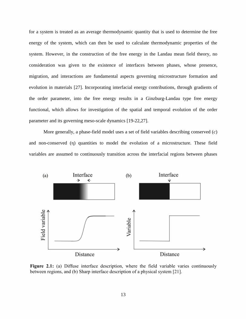
variables are assumed to continuously transition across the interfacial regions between phases
Figure 2.1: (a) Diffuse interface description, where the field variable varies continuously
between regions, and (b) Sharp interface description of a physical system [21].

14
leading to the diffuse interface description, shown in Figure 2.1, which allows for the evolution
of complex processes to be numerically modeled and predicted [19-22, 27]. These field variables
are used to construct a free energy functional that contains all of the relevant local and non-local
thermodynamic and energetic information for a system that will influence the evolution to a
minimum energy configuration, for example: bulk and interfacial energies, elastic interactions,
electrostatic interactions, magnetic fields, etc. [19-22,27]. A simple expression for a free energy
functional is given in Equation 2.1 [20].
𝐹 = ∫ (𝑓(𝑐1, … , 𝑐𝑛, 𝜂1, … , 𝜂𝑝) + ∑ 𝛼𝑖(𝛁𝑐𝑖)2
𝑛
𝑖=1
+ ∑ ∑ 𝛽𝑖𝑗
𝑝
𝑘=1
3
𝑖,𝑗=1
𝛁𝑖𝜂𝑘𝛁𝑗𝜂𝑘) 𝑑Ω (Equation 2.1)
Here, 𝑓 is the local free-energy density, which is a function of the field variables and is usually
taken to have the form of a double well potential for each interaction that describes bulk energy
differences. The function, 𝑓, also provides an energetic barrier between the stable and/or meta-
stable phases that are present. This is schematically shown in Figure 2.2 for a two-phase system
with solid and liquid phases where, depending on the temperature, either the solid or liquid phase
is stable (i.e., an energetic minimum) with a corresponding energy barrier that needs to be
overcome for a phase transformation to occur [21]. The second and third terms in Equation 2.1,
which are gradients of the field variables, capture interfacial energy contributions that arise from
compositional or structural changes, respectively. The interfacial gradient coefficients, 𝛼𝑖 and
𝛽𝑖𝑗 , are related to interfacial thicknesses and energies, which in general may be anisotropic.
These coefficients are always positive, thus causing interfaces to be energetically unfavorable,

15
which provides a driving force for evolution (i.e., the system wants to reduce the interfacial
energy) [19-22,27].
With a physically relevant free energy functional constructed, the spatial and temporal
evolution of the field variables, and thus the physical quantities, is obtained by solving either the
Allen-Cahn expression in Equation 2.2 or the Cahn-Hilliard expression in Equation 2.3,
depending on the physical processes to be modeled. These equations describe the evolutionary
dynamics of non-conserved and conserved quantities, respectively [20,27].
𝜕𝜂𝑝(𝒓, 𝑡)
𝜕𝑡= −𝑀𝑝𝑞
𝛿𝐹
𝛿𝜂𝑞(𝒓, 𝑡) (Equation 2.2)
𝜕𝑐𝑖(𝒓, 𝑡)
𝜕𝑡= 𝛁 ∙ (𝑀𝑖𝑗𝛁
𝛿𝐹
𝛿𝑐𝑗(𝒓, 𝑡)) (Equation 2.3)
Figure 2.2: Schematic representation of a free energy density above, at, and below the phase
transition temperature for a solid-liquid system. The double-well potential has minima at 𝜙 = 0
and 𝜙 = 1 corresponding to the stable liquid and solid phases, respectively.

16
Here, 𝑀 are kinetic coefficients that can be related to atomic or interfacial mobilities and the 𝛿𝐹
terms represent the functional derivatives of the free energy functional with respect to the
appropriate field variable. To model the spatial and temporal evolution of a physical system
described by these equations of motion, Equations 2.2 and 2.3 must be solved using numerical
methods for solving differential equations, for example, explicit or implicit finite difference
methods, spectral methods, or finite element methods [19-22,27].
2.2 Physical Vapor Deposition
This research utilized the ballistic deposition / interfacial growth model of Keblinski et
al. [16] to capture relevant aspects of PVD growth processes and dynamics, including: arbitrary
surface morphology formation, surface tension and diffusion, and nonlocal shadowing effects.
This model was demonstrated to naturally capture these PVD growth aspects and allowed for the
study of varying deposition parameters on thin film morphology in addition to implicitly tracking
the interior structure (density) of the thin film. To model PVD within the phase-field framework,
this model introduced two field variables: 𝑓(𝒓, 𝑡) and g(𝒓, 𝑡). The first field variable, 𝑓(𝒓, 𝑡),
describes the growing thin film solid where 𝑓(𝒓, 𝑡) ≈ 1 defines a solid region, 𝑓(𝒓, 𝑡) ≈ −1
defines a region of vacuum or no solid, and 𝑓(𝒓, 𝑡) ≈ 0 naturally defines the solid-vapor
interface. The second variable, g(𝒓, 𝑡), describes the density of the incident vapor flux where
g(𝒓, 𝑡) ≈ 0 defines a region of no vapor flux and g(𝒓, 𝑡) > 0 defines the local density of incident
vapor being transported to the thin film surface. The free energy functional for this model, 𝐹𝑉𝐷,
was constructed as a function of the field variable 𝑓(𝒓, 𝑡) and its gradient, which provided a
symmetric double-well energy barrier between the equilibrium vapor and solid phases and is
given below in Equation 2.4, where a is the interfacial gradient coefficient for surface tension.

17
𝐹𝑉𝐷 = ∫ (−1
2𝑓2 +
1
4𝑓4 + 𝑎(𝛁𝑓)2) 𝑑Ω (Equation 2.4)
The spatial and temporal evolution of these field variables is governed by the coupled and
non-dimensional equations of motion in Equations 2.5 and 2.6, which describe the growth and
evolution of the solid field, 𝑓(𝒓, 𝑡), at the expense of the incident vapor field, g(𝒓, 𝑡), and the
evolution of the incident vapor field, g(𝒓, 𝑡), respectively.
𝜕𝑓
𝜕𝑡= 𝛁2
𝛿𝐹𝑉𝐷
𝛿𝑓+ 𝐵(𝛁𝑓)2g + 𝐶√(𝛁𝑓)2g𝜂 (Equation 2.5)
𝜕g
𝜕𝑡= 𝛁[𝐷𝛁g − 𝑨g] − 𝐵(𝛁𝑓)2g (Equation 2.6)
In Equation 2.5, the first term is from the Cahn-Hilliard evolution dynamics (Equation
2.3), which provides the model with the capability for arbitrary surface morphology formation
and accounts for both surface and bulk diffusion during thin film solid growth. The second term,
which couples Equations 2.5 and 2.6, serves as the source term that leads to the growth of the
thin film solid at the expense of the incident vapor flux, where the parameter 𝐵 controls the rate
of vapor-to-solid conversion. The last term provides surface fluctuations through an uncorrelated
Gaussian distribution, 𝜂(𝒓, 𝑡), where the amplitude is proportional to the square root of the
aggregation rate and the parameter, 𝐶, controls the overall strength of the noise. It should be
recognized that the second and third terms are only operational near an interface due to the
presence of 𝛁𝑓(𝒓, 𝑡) terms. Furthermore, in the case of no deposition, the solid phase defining
the thin film should be conserved with the presence of an interface between the stable solid and
vacuum regions, which is enabled by the symmetric double well potential in the free energy
18
functional and the Cahn-Hilliard dynamics. However, in the case of deposition, this double well
potential symmetry is broken (by the second and third terms), thus leading to the growth of the
stable solid phase for the thin film.
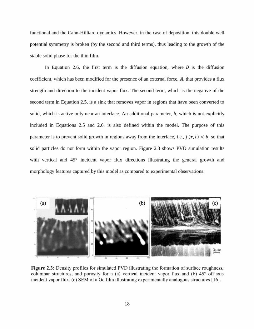
In Equation 2.6, the first term is the diffusion equation, where 𝐷 is the diffusion
coefficient, which has been modified for the presence of an external force, 𝑨, that provides a flux
strength and direction to the incident vapor flux. The second term, which is the negative of the
second term in Equation 2.5, is a sink that removes vapor in regions that have been converted to
solid, which is active only near an interface. An additional parameter, 𝑏, which is not explicitly
included in Equations 2.5 and 2.6, is also defined within the model. The purpose of this
parameter is to prevent solid growth in regions away from the interface, i.e., 𝑓(𝒓, 𝑡) < 𝑏, so that
solid particles do not form within the vapor region. Figure 2.3 shows PVD simulation results
with vertical and 45° incident vapor flux directions illustrating the general growth and
morphology features captured by this model as compared to experimental observations.
Figure 2.3: Density profiles for simulated PVD illustrating the formation of surface roughness,
columnar structures, and porosity for a (a) vertical incident vapor flux and (b) 45° off-axis
incident vapor flux. (c) SEM of a Ge film illustrating experimentally analogous structures [16].

19
2.3 Polycrystalline Materials
In this research, the evolution of subsurface grains, including grain growth and rotation,
and grain boundary (GB) motion, was based on the phase-field model of polycrystalline
materials developed by Warren et al. [23]. This model was shown to capture relevant aspects of
grain impingement and coarsening during microstructure evolution through GB migration and
grain rotation. To accomplish this, a free energy functional was constructed with two field
variables: 𝜙(𝒓, 𝑡) and 𝜃(𝒓, 𝑡) . The first field variable, 𝜙(𝒓, 𝑡) , distinguishes between the
structurally ordered regions within a grain interior where 𝜙(𝒓, 𝑡) ≈ 1 and structurally disordered
regions characteristic of a liquid or vapor where 𝜙(𝒓, 𝑡) ≈ 0 or at a GB where 0 < 𝜙(𝒓, 𝑡) < 1.
The second field variable, 𝜃(𝒓, 𝑡), describes the local grain orientation from a defined global axis
(the positive x-axis in Warren et al. [23] and this research) and varies between 0 and 2𝜋 𝑁𝑆⁄ ,
where 𝑁𝑆 is the rotational symmetry of the crystal. With these field variables, an isotropic free
energy functional, 𝐹𝑃𝐶 , was constructed, shown in Equation 2.7, for polycrystalline systems,
which is dependent on grain misorientation.
𝐹𝑃𝐶 = ∫ (𝑓(𝜙) +𝛼2
2|∇𝜙|2 + 𝑠g(𝜙)|∇𝜃| +
휀2
2ℎ(𝜙)|∇𝜃|2) 𝑑Ω (Equation 2.7)
The first two terms in Equation 2.7 comprise the traditional components of a free energy
functional, where ∇𝜙(𝒓, 𝑡) is the interfacial energy contribution and 𝑓(𝜙) can be taken as (i) a
single-well potential to model a polycrystalline system where a solid with grains and GBs is the
only allowable stable phase and grain growth occurs via curvature only with no temperature
influence or (ii) a double-well potential to model a polycrystalline system with temperature
dependence, where a disordered phase such as a liquid or vapor is allowed to coexist with the

20
ordered solid phase. The third and fourth terms were appended to the traditional components to
account for grain orientation and misorientation contributions within the free energy. The third
term was required for grains to be stable and the fourth term allowed for grain boundary
dynamics to occur. The coefficient functions g(𝜙) and ℎ(𝜙) were incorporated so that grain
orientation and misorientation effects are reduced or removed within a disordered region where
these have no physical meaning. This was accomplished in Warren et al. [23] and in this research
by taking both functions to be 𝜙(𝒓, 𝑡)2. Other functions could be used provided the selected
functions are monotonically increasing. The spatial and temporal evolution of these field
variables is governed by the Allen-Cahn dynamics (Equation 2.2) for non-conserved phenomena,
which gives rise to the non-dimensional equations of motion in Equations 2.8 and 2.9 for the
𝜙(𝒓, 𝑡) and 𝜃(𝒓, 𝑡) fields, respectively.
𝜏𝜙
𝜕𝜙
𝜕𝑡=
𝜕𝑓
𝜕𝜙+ 𝛼2∇2𝜙 − 2𝑠𝜙|∇𝜃| − 휀2𝜙|∇𝜃|2 (Equation 2.8)
𝑃(|∇θ|)𝜏𝜃𝜙2𝜕𝜃
𝜕𝑡= ∇ ∙ [𝜙2 (
𝑠
|∇𝜃|+ 휀2) ∇𝜃] (Equation 2.9)
The non-dimensional coefficients 𝜏𝜙, 𝜏𝜃, 𝛼, s, and 휀 in Equations 2.8 and 2.9 can be related to
thermodynamic and physical quantities, such as the latent heat of a phase transformation, 𝐿, and
a grain boundary feature size (e.g., GB thickness), 휀∗, that correspond to the specific material
being modeled. To do this, the dimensional coefficients, denoted by tildes, are first determined in
the following manner as prescribed by Warren et al. [23]: 휀̃ = 휀∗√𝐿 , �̃� = 1.875휀̃ , and �̃� =
1.25𝑎휀̃ where 𝑎 = √𝐿 2⁄ . Next, the dimensional quantities are non-dimensionalized according
to the following prescription (Equation 2.10) to be used in Equations 2.8 and 2.9.

21
(�̃�, �̃�, �̃�) = (𝑙0𝑥, 𝑙0𝑥, 𝑙0𝑥) �̃� = 𝑡𝑜𝑡 �̃�𝜙 = 𝑎2𝑡0𝜏𝜙 �̃�𝜙 = 𝑎2𝑡0𝜏𝜙
(Equation 2.10)
휀̃ = 𝑎𝑙𝑜휀 �̃� = 𝑎𝑙𝑜𝛼 �̃� = 𝑎2𝑙𝑜𝑠
Here, 𝑙𝑜 and 𝑡𝑜 are characteristic length and time scales describing the system being modeled.
The kinetic coefficient function, 𝑃(|∇𝜃|), locally amplifies or reduces the kinetics at GBs and
grain interiors to influence grain growth as a whole, i.e., it allows the individual modification of
GB migration and grain rotation effects and has the form given in Equation 2.11, where the
parameters 𝛽 and 𝜇 can be chosen to increase or decrease the propensity for grain rotation and
the rate of GB migration.
𝑃(|∇𝜃|) = 1 − 𝑒−𝛽𝜀|∇𝜃| +𝜇
휀𝑒−𝛽𝜀|∇𝜃| (Equation 2.11)
As discussed above, the function 𝑓(𝜙) can be taken as a single-well or double-well
potential depending on the physical circumstances. The non-dimensional forms of this function
considered by Warren et al. [23] are: 𝑓(𝜙) = (1 2⁄ )(1 − 𝜙)2 for a single-well potential and
𝑓(𝜙) = (1 2⁄ )𝜙2(1 − 𝜙)2 + 𝑓𝑠𝑜𝑙 𝑝(𝜙) for a double-well potential, where 𝑓𝑠𝑜𝑙 = 2(𝑇 𝑇𝑚⁄ − 1)
is also in non-dimensional form and defines the free energy of the solid phase away from an
interface with a thermodynamic driving force (i.e., undercooling). Furthermore, the free energy
within the disordered phase is assumed to be zero while the free energy within the solid phase is
provided by 𝑓𝑠𝑜𝑙 . Therefore, 𝑓𝑠𝑜𝑙 is multiplied by the function 𝑝(𝜙), which is a polynomial
approximation to a step function with 𝑝(0) = 0 and 𝑝(1) = 1 to enforce this condition. Two
forms of 𝑝(𝜙) were considered by Warren et al. [23], which gave similar results, Type I: 𝑝(𝜙) =

22
𝜙3(10 − 15𝜙 + 6𝜙2) and Type II: 𝑝(𝜙) = 𝜙2(3 − 2𝜙) . As an application of this model,
Figure 2.4 shows simulation results from Warren et al. [23] using the single-well potential for a
polycrystalline system with only a single solid phase present and the double well potential with a
polycrystalline system for the solidification of an undercooled liquid, i.e. isotropic growth and
coarsening of nuclei.
2.4 Materials with Multiple Solid Phases
The next component utilized in this research is the phase-field model developed by
Steinbach et al. [24] for modeling multiphase systems, which can be used to quantitatively model
solid-solid and solid-liquid phase transformations. While this model captures interfacial energies
and growth for systems with 𝑁 phases (𝑁 > 1), it was extended in later work by Steinbach et al.
[24] to more accurately account for the conservation of interfacial stresses of triple junctions. In
Figure 2.4: (Top) Evolution of a polycrystalline system with only a single solid phase using the
single-well potential, and (Bottom) evolution of a polycrystalline system with both solid and
liquid phases using the double-well potential. Colors represent different grain orientations [23].

23
this multiphase model, each of the 𝑁 possible phases is assigned a unique field variable, 𝑝𝑖(𝒓, 𝑡)
that varies between 0 and 1. These field variables correspond to the local volume fraction of each
phase allowing different phases to be distinguished. Therefore, to make use of this phase fraction
interpretation of the field variables, the condition that all 𝑁 field variables must sum to unity is
required at any given location within the system.
∑ 𝑝𝑖(𝒓, 𝑡)
𝑁
𝑖=1
= 1 (Equation 2.12)
With an arbitrary number of phases, a free energy functional, 𝐹𝑀𝑃, is constructed with these field
variables by considering a sum over all pairwise interactions between the phases, thus providing
kinetic and potential energy terms that are dependent on the local field variables, 𝑝𝑖(𝒓, 𝑡), their
gradients, and possibly temperature.
𝐹𝑀𝑃 = ∑ (휀𝑖𝑘
2
2|𝑝𝑘𝛁𝑝𝑖 − 𝑝𝑖𝛁𝑝𝑘|2
𝑁
𝑖<𝑘
+1
4𝑎𝑖𝑘[𝑝𝑖
2𝑝𝑘2 − 𝑚𝑖𝑘 (
1
3𝑝𝑖
3 −1
3𝑝𝑘
3 + 𝑝𝑖2𝑝𝑘 − 𝑝𝑘
2𝑝𝑖)])
(Equation 2.13)
These kinetic and potential energy terms capture the interfacial and bulk energies and their
differences for the phases that are present in the local volume to define the energy barriers for the
phase transformations where the potential energy term in this construction provides a double-
well potential for each pair of phases. With this free energy functional, the spatial and temporal
evolution of these field variables is governed by the Allen-Cahn dynamics (Equation 2.2) for

24
non-conserved phenomena, thus giving rise to the following set of non-dimensional equations of
motion.
𝜕𝑝𝑖
𝜕𝑡= ∑
1
𝜏𝑖𝑘[휀𝑖𝑘
2 (𝑝𝑘𝛁2𝑝𝑖 − 𝑝𝑖𝛁2𝑝𝑘) −
𝑝𝑖𝑝𝑘
2𝑎𝑖𝑘
(𝑝𝑘 − 𝑝𝑖 − 2𝑚𝑖𝑘)]
𝑁
𝑘≠𝑖
(Equation 2.14)
The parameters in Equation 2.14 are as follows: 𝜏𝑖𝑘 is a kinetic coefficient, 휀𝑖𝑘2 defines the
numerical interface thickness, 𝑎𝑖𝑘 is a positive constant, and 𝑚𝑖𝑘 is the coefficient for deviation
from thermodynamic equilibrium that provides the local driving force as a function of
temperature. These numerical parameters are related to physical and thermodynamic quantities.
𝜏𝑖𝑘 =𝐿𝑖𝑘𝜆𝑖𝑘
𝑇𝑖𝑘𝜇𝑖𝑘 휀𝑖𝑘
2 = 𝜆𝑖𝑘𝜎𝑖𝑘 𝑎𝑖𝑘 =𝜆𝑖𝑘
72𝜎𝑖𝑘 𝑚𝑖𝑘 =
6𝑎𝑖𝑘𝐿𝑖𝑘(𝑇𝑖𝑘 − 𝑇)
𝑇𝑖𝑘 (Equation 2.15)
The physical quantities shown in Equation 2.15 are as follows: 𝐿𝑖𝑘 is the latent heat released or
consumed during the i-k phase transformation, 𝜆𝑖𝑘 is the i-k interface thickness, 𝑇𝑖𝑘 is the
temperature at which the i-k phase transformation takes place, 𝜇𝑖𝑘 is the i-k interface mobility,
and 𝜎𝑖𝑘 is the i-k interfacial energy. All of these physical parameters are dependent on the phases
and/or materials that comprise the system and the i-k interface. As such, these quantities are
required for every material, phase and interface to develop a quantitative phase-field model. To
demonstrate the utility of this model, Figure 2.5 illustrates simulation results for the isothermal
solidification of four particles with two different solid phases in an undercooled liquid.
During the vapor deposition process, substrates may be heated to a desired temperature,
which plays a significant role in the surface morphology, phase nucleation, and microstructure

25
evolution within the growing thin film solid [5,6,9]. Additionally, latent heat is either released or
absorbed by the thin film during the vapor deposition and subsurface phase transformations that
can contribute to thermal fluctuations and gradients within the system [28]. As such, the
influence of temperature distributions and evolution is a necessary feature to be considered in a
model describing solid growth during the PVD process. To incorporate temperature evolution in
this research, the multiphase equations of motion in Equation 2.14 are coupled to a temperature
field, 𝑇(𝒓, 𝑡), through the heat conduction equation that is modified to provide a heat source /
sink as shown in Equation 2.16 [28].
𝜌𝑖𝐶𝑃
𝜕𝑇
𝜕𝑡= 𝑘𝑇𝛁2𝑇 + 𝐿𝑖𝑘
𝜕𝑝𝑖
𝜕𝑡 (Equation 2.16)
In Equation 2.16, the physical quantities for the ith phase are as follows: 𝜌𝑖 is the density, 𝐶𝑃 is
the heat capacity, 𝑘𝑇 is the thermal conductivity, and 𝐿𝑖𝑘 is the latent heat of the i-k phase
transformation. These parameters must be defined for each phase and phase transformation being
Figure 2.5: Simulation results of isothermal solidification and impingement of four isotropic
solid particles with two different phases (red and yellow) in an undercooled liquid (blue) via the
multiphase phase-model with toy parameters.

26
considered by the model. From the last term in Equation 2.16, the heat source / sink depends on
the latent heat and contributes to temperature evolution only when the field variables, 𝑝𝑖(𝒓, 𝑡),
are changing in time (e.g., at an interface where a phase transformation is occurring); otherwise
Equation 2.16 is the traditional heat conduction equation.
2.5 Phase Nucleation
To capture thermally activated phase nucleation events during PVD thin film growth, this
research utilized the nucleation approach of Simmons et al. [25,26], which explicitly introduces
fully formed nucleation sites of other possible phases into a phase-field model via classical
nucleation theory and Poisson seeding. In this method, the classical nucleation rate, 𝐽, is given as
[25,26,29],
𝐽 =3(∆𝐺𝑛𝑢𝑐)2
4√𝜋𝑘𝐵𝑇(𝐴𝜎𝑖𝑘)3
2⁄𝑁𝛽𝑒
(−∆𝐺∗
𝑘𝐵𝑇) (Equation 2.17)
Here, the ratio term is the Zeldovich non-equilibrium factor that accounts for the probability of
nuclei to grow or dissolve, where ∆𝐺𝑛𝑢𝑐 is the difference in free energy required to form a
nucleus of arbitrary size, 𝑘𝐵 is Boltzmann’s constant, 𝑇 is temperature, 𝐴 is a geometric factor
that accounts for the shape of the nucleus, and 𝜎𝑖𝑘 is the interfacial energy between the i-k
phases. The remaining parameters are as follows: 𝑁 is the number of atoms in the local phase-
field volume, 𝛽 is the rate of critical nuclei formation, and ∆𝐺∗ is the energy barrier required to
form a stable nucleus of critical size. In two-dimensions this can be calculated as: ∆𝐺∗ =
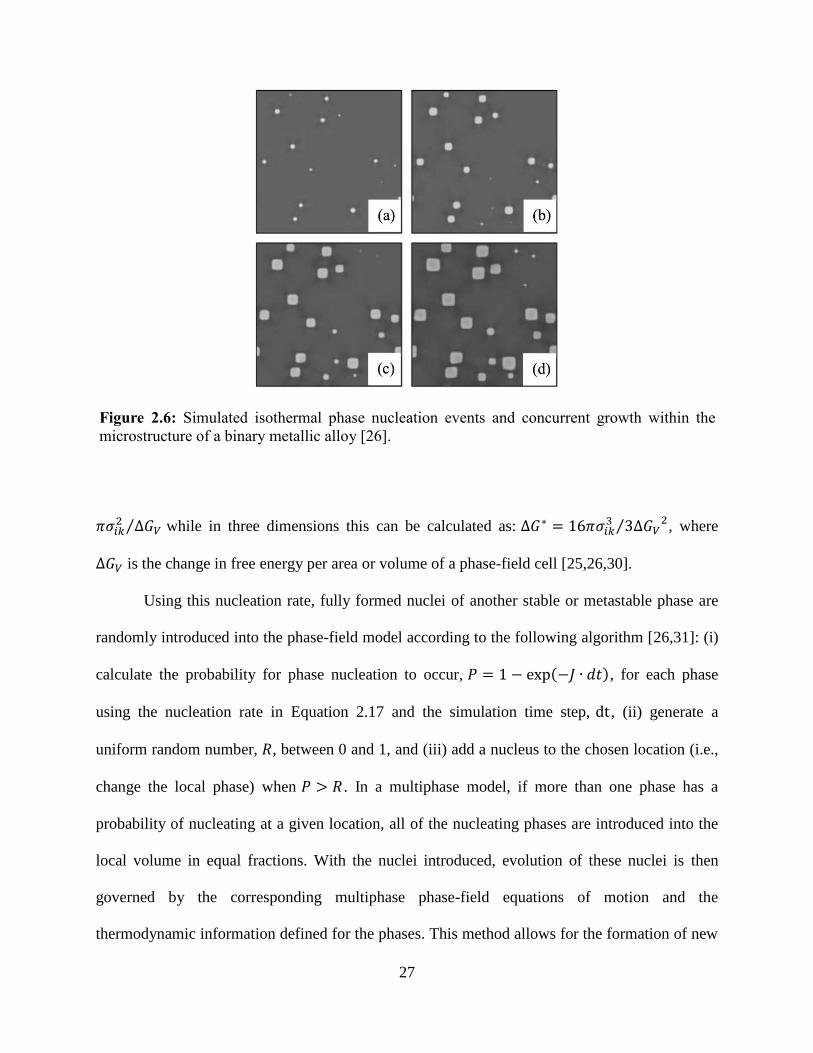
27
𝜋𝜎𝑖𝑘2 ∆𝐺𝑉⁄ while in three dimensions this can be calculated as: ∆𝐺∗ = 16𝜋𝜎𝑖𝑘
3 3∆𝐺𝑉2⁄ , where
∆𝐺𝑉 is the change in free energy per area or volume of a phase-field cell [25,26,30].
Using this nucleation rate, fully formed nuclei of another stable or metastable phase are
randomly introduced into the phase-field model according to the following algorithm [26,31]: (i)
calculate the probability for phase nucleation to occur, 𝑃 = 1 − exp(−𝐽 ∙ 𝑑𝑡), for each phase
using the nucleation rate in Equation 2.17 and the simulation time step, dt , (ii) generate a
uniform random number, 𝑅, between 0 and 1, and (iii) add a nucleus to the chosen location (i.e.,
change the local phase) when 𝑃 > 𝑅 . In a multiphase model, if more than one phase has a
probability of nucleating at a given location, all of the nucleating phases are introduced into the
local volume in equal fractions. With the nuclei introduced, evolution of these nuclei is then
governed by the corresponding multiphase phase-field equations of motion and the
thermodynamic information defined for the phases. This method allows for the formation of new
Figure 2.6: Simulated isothermal phase nucleation events and concurrent growth within the
microstructure of a binary metallic alloy [26].

28
nuclei while previous nuclei evolve during the simulation (e.g., grow or dissolve). Figure 2.6
illustrates simulation results of concurrent nucleation and growth in a binary metallic alloy using
the phase nucleation approach outlined above.

29
Chapter 3: Formulation and Implementation of Phase-Field Models for Physical Vapor
Deposition and Microstructure Evolution
3.1 Introduction
This chapter outlines the necessary mathematical and numerical components to develop
novel phase-field models for physical vapor deposition (PVD) and microstructure evolution in
this research. The initial approach employed in this research is to combine the phase-field
models described in Chapter 2 using simple coupling conditions between the relevant models.
This initial and novel approach is viewed as one method to develop a phase-field model that
combines different physical processes into a single model, while Chapter 6 provides an
alternative method to improve upon this initial construction. The coupling conditions developed
in this research are outlined in Section 3.2 for PVD of polycrystalline materials (i.e., coupling
Sections 2.2 and 2.3) and Section 3.3 for PVD of multiphase materials (i.e., coupling Sections
2.2 and 2.4). Section 3.4 outlines the mathematical constraint and numerical implementation

30
developed and used in this research for enforcing the phase fraction description of the multiphase
model in Section 2.4. Finally, Section 3.5 briefly discusses finite difference methods and the
method of conjugate gradients, which are the numerical methods implemented in this research to
solve the phase-field equations of motion.
3.2 Physical Vapor Deposition and Polycrystalline Evolution
As a first approach in the development of a unified phase field model for PVD, the
models described in Sections 2.2 and 2.3 are coupled to create a sequential phase-field
simulation algorithm where, within the same time step, PVD of the thin film occurs first,
followed by evolution (grain growth, grain rotation, etc.) of the underlying polycrystalline
microstructure. The PVD model described in Section 2.2 is taken to control all PVD growth
processes between the solid and vapor phases. Thus, this determines the allowable solid growth
and evolution of the thin film at a given location. The grain evolution model described in Section
2.3 is taken to control all grain evolution below the thin film surface within the solid
microstructure regions as defined by the PVD model. Therefore, the solid growth determined by
the PVD model constrains the evolution of the polycrystalline model to occur only within those
solid regions. With this initial approach, features developed in the PVD model may influence
grain evolution but microstructure features (e.g., grain boundaries and grain orientation) do not
influence surface growth and dynamics.
To apply this constraint, a simple coupling approach between the models is defined. The
local solid density, 𝑓𝑑(𝒓, 𝑡) , in the PVD model is introduced as 𝑓𝑑(𝒓, 𝑡) = (𝑓(𝒓, 𝑡) + 1) 2⁄ ,
which has values between 0 and 1 [16]. This local solid density defines the fraction of a phase-
field volume that is solid (i.e., structurally ordered), where the difference 1 − 𝑓𝑑(𝒓, 𝑡) is
31
considered to be the fraction of vapor or vacuum phase. Therefore, the local solid density has a
similar interpretation as the 𝜙(𝒓, 𝑡) field variable in the grain evolution model, which defines the
fraction of the phase-field volume that is solid [23]. Therefore, to couple the PVD and grain
evolution models in Sections 2.2 and 2.3, respectively, this research enforces the condition that
𝜙(𝒓, 𝑡) ≤ 𝑓𝑑(𝒓, 𝑡) for every phase-field volume at every time step. It should be noted that these
variables cannot be taken to be strictly equal during the simulation as the 𝜙(𝒓, 𝑡) variable needs
to evolve freely within the solid regions, specifically decreasing to values less than 𝑓𝑑(𝒓, 𝑡) at
grain boundaries, so grain boundary dynamics are not artificially influenced. Therefore, the
kinetic coefficient parameters, 𝜏𝜙 and 𝜏𝜃, are chosen so that correlated growth of the thin film
solid and evolution of the underlying microstructure occurs.
3.3 Physical Vapor Deposition and Multiphase Evolution
A similar approach is taken to present a phase-field model for PVD of multiphase thin
films. The models described in Sections 2.2 and 2.4 are coupled to create a sequential phase-field
simulation algorithm where, within the same time step, PVD of the thin film occurs first,
followed by evolution of the underlying phases including phase nucleation events (Section 2.5)
within the microstructure. The PVD model described in Section 2.2 controls all PVD growth
processes, thus determining the allowable growth and evolution of the thin film at a given
location. The model described in Section 2.4 is used to control all multiphase evolution beneath
the thin film surface within the solid microstructure regions defined by the PVD model. Phase
nucleation events occur once evolution of the phases has taken place; nucleated phases begin
evolving on the next time step. Therefore, the solid growth determined by the PVD model
constrains the evolution of the multiphase model to occur only within those regions containing

32
solid. With this initial approach, features developed in the PVD model may influence phase
evolution (bulk or interfaces) but the presence of differing phases at the surface and interfaces
does not influence PVD growth dynamics.
To apply this constraint, a similar coupling approach to that in the prior section is
defined. The local solid density, 𝑓𝑑(𝒓, 𝑡) , in the PVD model is defined as 𝑓𝑑(𝒓, 𝑡) =
(𝑓(𝒓, 𝑡) + 1) 2⁄ , which has values between 0 and 1 [16]. This solid density describes the fraction
of the local phase-field volume that is solid (i.e., structurally ordered), where the difference 1 −
𝑓𝑑(𝒓, 𝑡) is considered to be the fraction of vapor or vacuum phase. With this, the local solid
density has a similar interpretation as the 𝑝𝑖(𝒓, 𝑡) field variables in the multiphase model, which
define the volume fraction of each phase at a given location [24]. Therefore, to couple these PVD
and multiphase evolution models, this work enforces the condition that, at every time step, the
sum of all field variables, 𝑝𝑖(𝒓, 𝑡) , describing only solid phases must equal the local solid
density, 𝑓𝑑(𝒓, 𝑡), i.e.,
∑ 𝑝𝑖(𝒓, 𝑡)
𝑁
𝑖=2
= 𝑓𝑑(𝒓, 𝑡) (Equation 3.1)
where 𝑝1(𝒓, 𝑡) is assumed to describe the vapor phase and all 𝑝𝑖 with 𝑖 > 1 describe the solid
phases within the microstructure of the growing thin film. Finally, 𝑝1 + 𝑝𝑖 (for i = 2, 𝑁), must
continue to equal unity as defined by the original phase-fraction constraint in Equation 2.12 for
all multiphase field variables, 𝑝𝑖(𝒓, 𝑡).
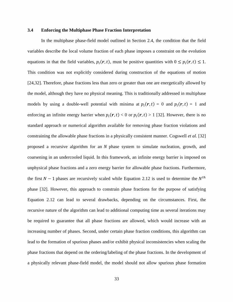
33
3.4 Enforcing the Multiphase Phase Fraction Interpretation
In the multiphase phase-field model outlined in Section 2.4, the condition that the field
variables describe the local volume fraction of each phase imposes a constraint on the evolution
equations in that the field variables, 𝑝𝑖(𝒓, 𝑡), must be positive quantities with 0 ≤ 𝑝𝑖(𝒓, 𝑡) ≤ 1.
This condition was not explicitly considered during construction of the equations of motion
[24,32]. Therefore, phase fractions less than zero or greater than one are energetically allowed by
the model, although they have no physical meaning. This is traditionally addressed in multiphase
models by using a double-well potential with minima at 𝑝𝑖(𝒓, 𝑡) = 0 and 𝑝𝑖(𝒓, 𝑡) = 1 and
enforcing an infinite energy barrier when 𝑝𝑖(𝒓, 𝑡) < 0 or 𝑝𝑖(𝒓, 𝑡) > 1 [32]. However, there is no
standard approach or numerical algorithm available for removing phase fraction violations and
constraining the allowable phase fractions in a physically consistent manner. Cogswell et al. [32]
proposed a recursive algorithm for an 𝑁 phase system to simulate nucleation, growth, and
coarsening in an undercooled liquid. In this framework, an infinite energy barrier is imposed on
unphysical phase fractions and a zero energy barrier for allowable phase fractions. Furthermore,
the first 𝑁 − 1 phases are recursively scaled while Equation 2.12 is used to determine the 𝑁𝑡ℎ
phase [32]. However, this approach to constrain phase fractions for the purpose of satisfying
Equation 2.12 can lead to several drawbacks, depending on the circumstances. First, the
recursive nature of the algorithm can lead to additional computing time as several iterations may
be required to guarantee that all phase fractions are allowed, which would increase with an
increasing number of phases. Second, under certain phase fraction conditions, this algorithm can
lead to the formation of spurious phases and/or exhibit physical inconsistencies when scaling the
phase fractions that depend on the ordering/labeling of the phase fractions. In the development of
a physically relevant phase-field model, the model should not allow spurious phase formation
34
(i.e., if the phase is not present it should not deterministically appear) nor should the physical
results depend on the ordering/labeling of the phase-field variables [33]. These drawbacks are
illustrated in the following examples. First, if 𝑝1(𝒓, 𝑡) = 0.6, 𝑝2(𝒓, 𝑡) = −0.1, and 𝑝3(𝒓, 𝑡) =
0.5, then following the approach of Cogswell et al. [32], these phase fractions are scaled to
𝑝1(𝒓, 𝑡) = 0.6, 𝑝2(𝒓, 𝑡) = 0.0, and 𝑝3(𝒓, 𝑡) = 0.4. However, if 𝑝1(𝒓, 𝑡) = 0.6 , 𝑝2(𝒓, 𝑡) = 0.5 ,
and 𝑝3(𝒓, 𝑡) = −0.1 , then this approach scales these phase fractions to 𝑝1(𝒓, 𝑡) = 0.55 ,
𝑝2(𝒓, 𝑡) = 0.0 , and 𝑝3(𝒓, 𝑡) = 0.45 . Furthermore, if 𝑝1(𝒓, 𝑡) = 0.5 , 𝑝2(𝒓, 𝑡) = 0.4 , and
𝑝3(𝒓, 𝑡) = 0.0, this approach scales these phase fractions to 𝑝1(𝒓, 𝑡) = 0.5, 𝑝2(𝒓, 𝑡) = 0.4, and
𝑝3(𝒓, 𝑡) = 0.1 while 𝑝1(𝒓, 𝑡) = 0.5, 𝑝2(𝒓, 𝑡) = 0.0, and 𝑝3(𝒓, 𝑡) = 0.4 becomes 𝑝1(𝒓, 𝑡) = 0.5,
𝑝2(𝒓, 𝑡) = 0.0, and 𝑝3(𝒓, 𝑡) = 0.5.
Therefore, this research proposes and utilizes an approach for removing phase fraction
violations and constraining the allowable phase fractions in an N phase system that (i) is easy to
numerically implement, (ii) requires only one iteration, (iii) imposes a traditional infinite energy
Figure 3.1: Code for the algorithms developed in this research for: (a) enforcing the phase
fraction condition in Equation 2.12, and (b) enforcing the phase fraction conditions in Equations
3.1 and 2.12 to allow coupling of the PVD and multiphase phase-field models as described in
Section 3.3.

35
barrier for unphysical phase fractions and a zero energy barrier for allowable phase fractions, (iv)
scales all phase fractions proportionately according to their initial phase fraction values; thus
removing any spurious phase formation and phase ordering/labeling dependence, and (v) easily
extends to allow coupling of the PVD and multiphase phase-field models as described in Section
3.3. Code for this algorithm is shown in Figure 3.1 (a). With this algorithm, unphysical phase
fractions less than zero are removed first. Then, each phase fraction is scaled according to the
ratio of their initial value and the sum of all phase fraction values; thus ensuring that all phase
fractions are allowed and satisfy Equation 2.12. Using this new approach, the phase fractions in
the above examples are now scaled, regardless of their order/label, to 𝑝1(𝒓, 𝑡) = 0. 54̅̅̅̅ ,
𝑝2(𝒓, 𝑡) = 0.0 , 𝑝3(𝒓, 𝑡) = 0. 45̅̅̅̅ and 𝑝1(𝒓, 𝑡) = 0. 55̅̅̅̅ , 𝑝2(𝒓, 𝑡) = 0. 44̅̅̅̅ , 𝑝3(𝒓, 𝑡) = 0.0 . The
algorithm, shown in Figure 3.1 (a), is easily modified to enforce the coupling condition outlined
in Section 3.3, where the local solid density, 𝑓𝑑(𝒓, 𝑡), becomes the quantity to which the phase
fractions describing solid phases are required to sum (recall Equation 3.1). With this modified
algorithm, unphysical solid phases less than zero are removed first. Then, each solid phase
fraction is scaled in relation to the local solid density so that phase evolution occurs only within
the solid region as defined by the PVD model. With the solid phase fractions evolved and
constrained, the vapor phase fraction is determined through enforcing Equation 2.12. Code for
this algorithm is shown in Figure 3.1 (b).
3.5 Numerical Solution Techniques
Numerical methods are techniques in which mathematical expressions, which may
describe complex physically relevant systems, are approximated in such a way so that the
problem is converted to one of performing a series of simple arithmetic operations [34,35].
36
Numerical methods are used, for example, to solve problems in linear algebra (i.e., systems of
linear equations), to find the zeros of polynomials and to approximate integrals and differential
equations [34,35]. Here, the focus is to numerically solve the differential equations that govern
the dynamics associated with PVD and microstructure evolution processes as discussed in
Chapter 2 using a finite difference approach. Specific applications of these approximations to the
PVD and microstructure equations from Chapter 2 are outlined in Chapters 4 - 6 where
appropriate. In the finite difference approach, the differential equations are discretized and
solved on a grid arising from this discretization. Furthermore, the solution of a differential
equation at a given point on the grid can be determined by considering information about the
function at the grid point and neighboring grid points [34,35]. As this technique is an
approximation to the true solution, errors will arise in the solution. These errors can be reduced
with smaller discretizations or by using information from more grid points, at the cost of added
computing time and complexity [34,35]. Below, finite difference approximations relevant to this
research (e.g., divided difference expressions, explicit and implicit Euler methods, etc.) are
derived along with a discussion of their error and stability. Finally, the iterative conjugate
gradient method is discussed, which is used in this research to solve the systems of equations that
arises from utilizing an implicit approximation.
3.5.1 Finite Difference Methods
The most straightforward approach to developing a finite difference approximation and
seeing the natural inclusion of a discretization is to consider the Taylor series expansion of a
general function, 𝑓(𝑞), where 𝑞 is a spatial or temporal coordinate with the other coordinates
suppressed [34,35]. Equation 3.2 illustrates the first four terms in the Taylor series expansion of

37
𝑓(𝑞 ± 𝑑𝑞), where 𝑑𝑞 is the interval between 𝑞 and 𝑞 ± 𝑑𝑞 (i.e., discrete points) and 𝑂(𝑑𝑞4)
represents the higher order terms beginning with the fourth derivative that are not listed here
[34,35].
𝑓(𝑞 ± 𝑑𝑞) = 𝑓(𝑞) ± 𝜕𝑓(𝑞)
𝜕𝑞𝑑𝑞 +
1
2!
𝜕2𝑓(𝑞)
𝜕𝑞2𝑑𝑞2 ±
1
3!
𝜕3𝑓(𝑞)
𝜕𝑞3𝑑𝑞3 + 𝑂(𝑑𝑞4) (Equation 3.2)
From Equation 3.2, different linear combinations can be constructed using values of the function
at different grid points to approximate derivatives [34,35]. For example, by considering the first
two terms in the Taylor series expansion, approximations to the first derivative can be developed
leading to the forward divided difference and backward divided difference approximations
shown in Equations 3.3 and 3.4, respectively [34,35].
𝜕𝑓(𝑞)
𝜕𝑞≅
1
𝑑𝑞(𝑓(𝑞 + 𝑑𝑞) − 𝑓(𝑞)) (Equation 3.3)
𝜕𝑓(𝑞)
𝜕𝑞≅
1
𝑑𝑞(𝑓(𝑞) − 𝑓(𝑞 − 𝑑𝑞)) (Equation 3.4)
The leading order term to the truncation error for these approximations can be determined by
including the next (third) term in the Taylor series expansion when algebraically solving for the
first derivative of 𝑓(𝑞) [34,35]. Performing this algebra gives the dominant truncation error as
±𝑑𝑞
2
𝜕2𝑓(𝑞)
𝜕𝑞2. Therefore, these approximations are said to be first order accurate as they have an
error of order 𝑑𝑞, i.e., 𝑂(𝑑𝑞). From this truncation error, it is shown that decreasing the interval,
𝑑𝑞, reduces the error in these approximations [34,35].

38
Equations 3.3 and 3.4 are often used to approximate time dependent derivatives, i.e., 𝑞 →
𝑡, to evolve a system forward in time [34,35]. In this context, Equation 3.3 calculates the next
time step value of the function, 𝑓(𝑡 + 𝑑𝑡), by using the current time step function value, 𝑓(𝑡),
and the current time step derivative value, 𝜕𝑓(𝑡)
𝜕𝑡. This is the forward or explicit Euler method, as
all current time step values of the function and its derivative are used in the solution [34, 35].
Equation 3.4 calculates the next time step function value, 𝑓(𝑡), by using the current time step
function value, 𝑓(𝑡 − 𝑑𝑡) , and the next time step value of the derivative, 𝜕𝑓(𝑡)
𝜕𝑡. This is the
backward or implicit Euler method, as the solution requires unknown information from the next
time step to calculate new values of the function at the next time step [34,35].
The stability of these Euler methods can be studied by considering the following simple
first order differential equation: 𝑓′(𝑡) = 𝜆𝑓(𝑡) [35]. Applying the explicit Euler method to this
differential equation, a general expression for 𝑓(𝑡 + 𝑑𝑡) at some point 𝑡𝑛 + 𝑑𝑡 is calculated as
𝑓(𝑡𝑛 + 𝑑𝑡) = 𝑓(𝑡𝑛)(1 + 𝜆𝑑𝑡). This expression provides the requirement that |1 + 𝜆𝑑𝑡| < 1, or
equivalently 𝑑𝑡 < 2|𝜆|⁄ , must be satisfied for the solution to be stable (i.e., the error does not
become amplified), thus making the explicit Euler method conditionally stable [35]. Applying
the implicit Euler method to this differential equation, a general expression for 𝑓(𝑡) at a given
point 𝑡𝑛 calculated as 𝑓(𝑡𝑛) = 𝑓(𝑡𝑛 − 𝑑𝑡)(1 − 𝜆𝑑𝑡)−1 . This expression provides the
requirement that |1 − 𝜆𝑑𝑡| > 1 must be satisfied for the solution to be stable. In general, 𝜆 may
be a complex number but if the real part of 𝜆 is less than 0, then the implicit Euler method will
always be stable, thus making it unconditionally stable [35]. This provides an improvement upon
the explicit Euler method in allowing for larger values of 𝑑𝑡 to be used [34,35]. Finally, it should
be noted that implicit methods might lead to an equation or system of equations that are not
39
easily solved, thus requiring the use of additional techniques, depending on the circumstances,
such as: the Newton or secant method, Gaussian elimination, the method of conjugate gradients,
etc. [34,35].
In the above construction for first derivative approximations, only the first two terms of
the Taylor series expansion in Equation 3.2 were considered. However, linear combinations of
𝑓(𝑞 + 𝑑𝑞) and 𝑓(𝑞 − 𝑑𝑞) can also be formed to produce additional approximations with higher
orders of accuracy [34,35]. For example, 𝑓(𝑞 + 𝑑𝑞) and 𝑓(𝑞 − 𝑑𝑞) can be subtracted to produce
a centered divided difference approximation to the first derivative as shown in Equation 3.5 or
𝑓(𝑞 + 𝑑𝑞) and 𝑓(𝑞 − 𝑑𝑞) can be added together to produce a centered divided difference
approximation to the second derivative as shown in Equation 3.6 [34,35].
𝜕𝑓(𝑞)
𝜕𝑞≅
1
2𝑑𝑞(𝑓(𝑞 + 𝑑𝑞) − 𝑓(𝑞 − 𝑑𝑞)) (Equation 3.5)
𝜕2𝑓(𝑞)
𝜕𝑞2≅
1
𝑑𝑞2(𝑓(𝑞 + 𝑑𝑞) − 2𝑓(𝑞) + 𝑓(𝑞 − 𝑑𝑞)) (Equation 3.6)
The leading order truncation error term for these approximations can be determined in the same
manner as Equations 3.3 and 3.4. Performing this algebra gives the dominant truncation error as
−1
6
𝜕3𝑓(𝑞)
𝜕𝑞3 𝑑𝑞2 for Equation 3.5 and −1
12
𝜕4𝑓(𝑞)
𝜕𝑞4 𝑑𝑞2 for Equation 3.6 [34,35]. From these
truncation error terms, the approximations in Equations 3.5 and 3.6 are second order accurate as
they have an error of order 𝑑𝑞2, i.e., 𝑂(𝑑𝑞2). Furthermore, it is also shown that a smaller 𝑑𝑞
value leads to a rapid decrease in the error contribution [34,35]. Equations 3.3 - 3.6 form the
basis of the numerical approximations used in this research for solving the governing differential
equations.
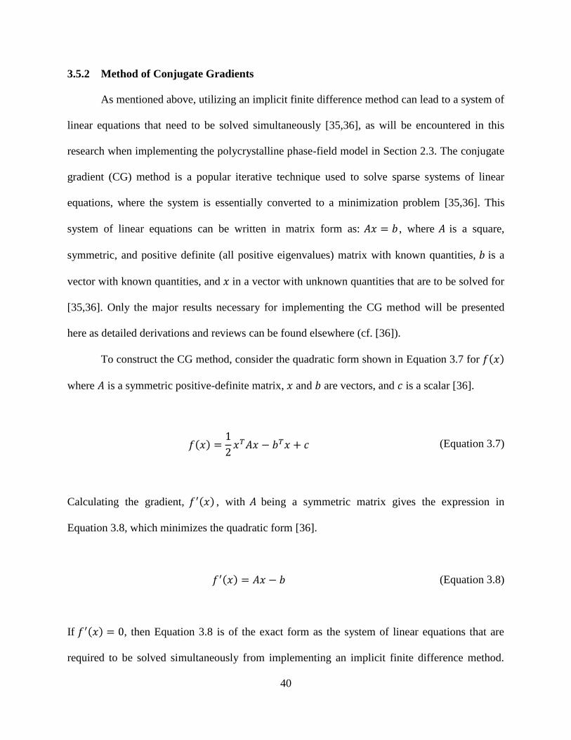
40
3.5.2 Method of Conjugate Gradients
As mentioned above, utilizing an implicit finite difference method can lead to a system of
linear equations that need to be solved simultaneously [35,36], as will be encountered in this
research when implementing the polycrystalline phase-field model in Section 2.3. The conjugate
gradient (CG) method is a popular iterative technique used to solve sparse systems of linear
equations, where the system is essentially converted to a minimization problem [35,36]. This
system of linear equations can be written in matrix form as: 𝐴𝑥 = 𝑏 , where 𝐴 is a square,
symmetric, and positive definite (all positive eigenvalues) matrix with known quantities, 𝑏 is a
vector with known quantities, and 𝑥 in a vector with unknown quantities that are to be solved for
[35,36]. Only the major results necessary for implementing the CG method will be presented
here as detailed derivations and reviews can be found elsewhere (cf. [36]).
To construct the CG method, consider the quadratic form shown in Equation 3.7 for 𝑓(𝑥)
where 𝐴 is a symmetric positive-definite matrix, 𝑥 and 𝑏 are vectors, and 𝑐 is a scalar [36].
𝑓(𝑥) =1
2𝑥𝑇𝐴𝑥 − 𝑏𝑇𝑥 + 𝑐 (Equation 3.7)
Calculating the gradient, 𝑓′(𝑥) , with 𝐴 being a symmetric matrix gives the expression in
Equation 3.8, which minimizes the quadratic form [36].
𝑓′(𝑥) = 𝐴𝑥 − 𝑏 (Equation 3.8)
If 𝑓′(𝑥) = 0, then Equation 3.8 is of the exact form as the system of linear equations that are
required to be solved simultaneously from implementing an implicit finite difference method.

41
Therefore, by determining the quantity, 𝑥, that minimizes 𝑓(𝑥), the solution to 𝐴𝑥 = 𝑏 is also
determined [36]. To do this, a line search method is used where an initial guess to the solution,
𝑥𝑖, is made, which is then improved upon (i.e., 𝑥𝑖+1) by moving a certain amount, 𝛼𝑖, along a
search direction, 𝑑𝑖, to minimize the error, 𝑒𝑖, and residual, 𝑟𝑖 [36]. This is shown mathematically
in Equation 3.9.
𝑥𝑖+1 = 𝑥𝑖 + 𝛼𝑖𝑑𝑖 (Equation 3.9)
The error provides an indication of how close the approximated solution, 𝑥𝑖 , is to the true
solution, 𝑥, while the residual provides an indication of how close the approximated value of 𝐴𝑥𝑖
to the true value of 𝑏 [36]. Expressions for the error and residual are given in Equations 3.10 and
3.11, respectively [36].
𝑒𝑖 = 𝑥𝑖 − 𝑥 (Equation 3.10)
𝑟𝑖 = 𝑏 − 𝐴𝑥𝑖 (Equation 3.11)
The parameter 𝛼𝑖 depends on the choice and/or construction of the search directions, 𝑑𝑖, which
leads to different methods, including: steepest descent (SD), conjugate directions (CDs), and
CGs. To construct the CG method, consider a set of 𝐴-orthogonal (conjugate) search directions,
𝑑𝑖 . That is, the search directions satisfy 𝑑𝑖𝑇𝐴𝑑𝑗 = 0 , thus leading to the requirement that
𝑑𝑖𝑇𝐴𝑒𝑖+1 = 0, i.e., the new error is A-orthogonal to the previous search direction [36]. In the CG
method, the search directions are constructed by conjugating the residuals using the Gram-
Schmidt process shown in Equation 3.12 [36].

42
𝑑𝑖 = 𝑟𝑖 + ∑ 𝛽𝑖𝑗
𝑖−1
𝑗=0
𝑑𝑗
(Equation 3.12)
where 𝛽𝑖𝑗 =𝑟𝑖
𝑇𝐴𝑑𝑗
𝑑𝑗𝑇𝐴𝑑𝑗
The residuals can be shown to have the properties that (i) each residual is orthogonal to the
previous search direction, i.e., 𝑑𝑖𝑇𝑟𝑗 = 0, and (ii) each residual is orthogonal to the previous
residual, i.e., 𝑟𝑖𝑇𝑟𝑗 = 0 . Furthermore, it can be shown that 𝑑𝑖
𝑇𝑟𝑖 = 𝑟𝑖𝑇𝑟𝑖 [36]. With these
conditions, simplified expressions for the search direction step size, 𝛼𝑖, the 𝛽𝑖𝑗 coefficients, and
the search direction 𝑑𝑖, can be determined and are given in Equations 3.13 - 3.15 [36].
𝛼𝑖 =𝑟𝑖
𝑇𝑟𝑖
𝑑𝑖𝑇𝐴𝑑𝑖
(Equation 3.13)
𝛽𝑖+1 =𝑟𝑖+1
𝑇 𝑟𝑖+1
𝑟𝑖𝑇𝑟𝑖
(Equation 3.14)
𝑑𝑖+1 = 𝑟𝑖+1 + 𝛽𝑖+1𝑑𝑖 (Equation 3.15)
Additionally, Equation 3.11 for the residual calculation is generally replaced by another
expression that allows for fewer matrix-vector multiplications to be performed when the CG
method is implemented [36]. To do this, Equation 3.9 is multiplied by −𝐴 and 𝑏 is added to both
sides of the equation. Then, Equation 3.11 is used to simplify this expression, thus giving
Equation 3.16 for the calculation of residuals [36].
𝑟𝑖+1 = 𝑟𝑖 − 𝛼𝑖𝐴𝑑𝑖 (Equation 3.16)

43
Therefore, Equations 3.9, 3.13, 3.14, 3.15, and 3.16 form the necessary components to
numerically implement the iterative CG method (cf. [35,36]). Although Equation 3.14, also
called the Fletcher-Reeves formula, is the only form listed here, as it’s the form used in this
research, other forms have been developed, such as the Polak-Ribiere formula, to allow for faster
converge of the CG method [36]. Finally, in order to initiate the CG method, initial guesses are
required for the solution vector, 𝑥0, the residual, 𝑟0, and the search direction, 𝑑0. In this research,
𝑥0 = 0, which gives the initial residual as 𝑟0 = 𝑏 and the initial search direction as 𝑑0 = 𝑟0 .
Additionally, since the CG method is an iterative technique, it is to be repeated until a very small
predefined tolerance, 𝑟𝑡𝑜𝑙, is satisfied via 𝑟𝑖𝑇𝑟𝑖 ≤ 𝑟𝑡𝑜𝑙, at which point the procedure stops.

44
Chapter 4: Phase-Field Simulations of Physical Vapor Deposition and Microstructure
Evolution of a Single-Phase Polycrystalline Metal
4.1 Introduction
This chapter presents simulation results for physical vapor deposition (PVD) of a generic
single-phase polycrystalline metal using the PVD and polycrystalline phase-field models
described in Sections 2.2 and 2.3, respectively, coupled via the sequential approach described in
Section 3.2. Furthermore, simulations are performed using both single-well and double-well
potentials described in Section 2.3 to provide a comparison of these approaches. First, Section
4.2 outlines the numerical methods implemented to solve the equations of motion, construction
of the initial system configurations, and the PVD and polycrystalline model parameters used.
Next, Section 4.3 presents simulation results performed on substrates with low-angle and high-
angle grain boundary (GB) misorientations. Section 4.4 presents simulation results performed
using substrates with varying substrate grain sizes. Finally, Section 4.5 presents simulation

45
results illustrating the effects of low and high PVD flux rates on the thin film microstructure and
surface feature formation.
4.2 Simulation Methodology and Model Parameters
The equations of motion described in Equations 2.5, 2.6, 2.8, and 2.9 are discretized and
solved on a uniform 100 x 100 square mesh. For the PVD model, Equations 2.5 and 2.6 are
solved using the explicit first-order Euler method (Equation 3.4) and centered second-order finite
difference (Equation 3.6) approximations for time and space, respectively. For both of these
equations, no-flux boundary conditions (i.e., the derivatives are taken to be zero) are applied in
the direction parallel to the substrate (x-axis) while fixed boundary conditions (i.e., the values of
the solution are defined) are applied perpendicular to the substrate (y-axis). For the
polycrystalline model, Equation 2.8 is solved with a semi-implicit approach (i.e., can still be
solved explicitly) while Equation 2.9 is solved using a fully implicit approach where the method
of conjugate gradients is implemented to solve the associated system of equations. No-flux
boundary conditions are applied at each boundary for both of these equations. The complete
discretization of Equations 2.8 and 2.9 is given in detail in Warren et al. [23].
In this research, the initial system configuration is that of a flat substrate parallel to and
spanning the x-axis with a thickness of 5 mesh points in the y-direction, where 𝑓(𝒓, 0) = 1 and
g(𝒓, 0) = 0. This condition is assumed to be constant below the 𝑦 = 1 boundary to provide a
fixed substrate region. Above the substrate is taken to be the vacuum region containing the
incident vapor flux, where 𝑓(𝒓, 0) = −1 and g(𝒓, 0) = g0. Beyond the 𝑦 = 100 boundary, this
condition is held fixed to provide a continuous source of vapor flux during deposition. Within the
initial substrate region, a polycrystalline microstructure is constructed, where 𝜙(𝒓, 0) = 1 and
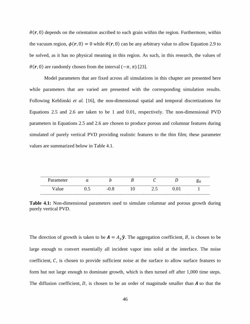
46
𝜃(𝒓, 0) depends on the orientation ascribed to each grain within the region. Furthermore, within
the vacuum region, 𝜙(𝒓, 0) = 0 while 𝜃(𝒓, 0) can be any arbitrary value to allow Equation 2.9 to
be solved, as it has no physical meaning in this region. As such, in this research, the values of
𝜃(𝒓, 0) are randomly chosen from the interval (−𝜋, 𝜋) [23].
Model parameters that are fixed across all simulations in this chapter are presented here
while parameters that are varied are presented with the corresponding simulation results.
Following Keblinski et al. [16], the non-dimensional spatial and temporal discretizations for
Equations 2.5 and 2.6 are taken to be 1 and 0.01, respectively. The non-dimensional PVD
parameters in Equations 2.5 and 2.6 are chosen to produce porous and columnar features during
simulated of purely vertical PVD providing realistic features to the thin film; these parameter
values are summarized below in Table 4.1.
Parameter 𝑎 𝑏 𝐵 𝐶 𝐷 g0
Value 0.5 -0.8 10 2.5 0.01 1
Table 4.1: Non-dimensional parameters used to simulate columnar and porous growth during
purely vertical PVD.
The direction of growth is taken to be 𝑨 = 𝐴𝑦�̂�. The aggregation coefficient, 𝐵, is chosen to be
large enough to convert essentially all incident vapor into solid at the interface. The noise
coefficient, 𝐶, is chosen to provide sufficient noise at the surface to allow surface features to
form but not large enough to dominate growth, which is then turned off after 1,000 time steps.
The diffusion coefficient, 𝐷, is chosen to be an order of magnitude smaller than 𝑨 so that the

47
primary source of vapor transport is the flux parameter, 𝑨 [16]. Finally, the density of the initial
vapor field, g0, is taken to be 1.
In Equations 2.8 and 2.9, the non-dimensional model parameters 휀 , 𝛼 and 𝑠 for
polycrystalline microstructure evolution are fixed by the choice of a GB feature size, 휀∗, and the
latent heat for a phase transformation, 𝐿. The physical quantities used in this research and the
calculated non-dimensional quantities are in line with the values used in Warren et al. [23]. In
this research, 휀∗ = 1 nm as this is a reasonable value for the GB thickness in metallic systems
[37-42]. To select a reasonable value for the latent heat, justification is provided by the fact that
the energetics for microstructure evolution in a metallic system are related to the melting point of
the corresponding material [5,23]. Therefore, in this research as in Warren et al. [23], 𝐿 is taken
to be the latent heat of fusion with a value of 2x10⁹ J/m3, which is reasonable for a metal.
Furthermore, these non-dimensional parameters depend on a characteristic length scale, 𝑙0, of the
system being modeled and is chosen to be 100 nm in this research, which is a reasonable value
for the size of grains within a vapor deposited metal as they can vary from several nanometers to
microns [41,42,44-46]. Using these physical quantities and the non-dimensionalization procedure
in Equation 2.10, the non-dimensional model parameters used in this research, truncated to 3
significant digits, are: 휀 = 0.0141, 𝛼 = 0.0265, and 𝑠 = 0.0176. The non-dimensional spatial
discretization is taken to be 0.05, which corresponds to a physical value of 5 nm and, therefore, a
physical simulation domain size of 0.5 𝜇 m x 0.5 𝜇 m. To determine an appropriate spatial
discretization for these simulations, values between 1 nm - 100 nm were used to determine
sufficient grain evolution dynamics within the PVD simulation domain size and time. The non-
dimensional temporal discretization is taken to be 0.01 (i.e., the same as in the PVD model). The
non-dimensional parameters controlling the rate of grain growth and grain evolution kinetics are

48
taken to be 𝜏𝜙 = 1, 𝜏𝜃 = 1, 𝜇 = 103, and 𝛽 = 105. Finally, the double-well potential requires a
temperature, 𝑇 , to drive the evolution of the system. As such, when using the double-well
potential, this research focuses on high temperature PVD with a constant ratio 𝑇 𝑇m⁄ = 59 60⁄
(i.e., 𝑇 ≈ 0.98𝑇m ), where 𝑇m is the phase transition temperature. Recall that the single-well
potential does not require this presence of a thermodynamic driving force.
4.3 Substrates with Low-Angle and High-Angle Misorientations
Using the modeling approach described in Sections 3.2 and 4.2, PVD simulations are
performed on polycrystalline substrates with low-angle GB misorientations, illustrated in Figures
4.1 and 4.2, and high-angle GB misorientations, illustrated in Figure 4.3 and 4.4, with both
single-well and double-well potentials. In each simulation, the deposition flux strength is taken
to be 𝐴𝑦 = −0.6 and the substrates contain 10 grains, each 50 nm in size with a randomly
assigned orientation. Several main features are observed during simulated PVD growth of these
films. First, as can be seen in Figures 4.1 - 4.4, grain coarsening occurs through grain rotation
and GB migration in an effort to reduce the interfacial energies, as expected, resulting in (i)
grains achieving a reasonably uniform internal orientation, and (ii) reduced GB misorientations.
This can be seen by comparing the initial microstructures in (a) to the resulting microstructures
in (d) for all figures. Furthermore, as the grains become sufficiently large, GB mobility decreases
and grain coarsening ceases (within the simulation time). As shown in Figures 4.1 - 4.4, the GBs
tend to migrate towards and become immobilized at the valleys between the surface columnar
features, thereby causing each columnar structure or neighboring structures to be associated with
a distinct grain orientation. Thus, the presence of a surface structure, such as columnar features,
influences GB migration within the microstructure and indicates the presence of distinct grain

49
Figure 4.1: Grain evolution (𝜃 field) during simulated PVD on a polycrystalline substrate with
a single-well potential, low-angle GB misorientations, and 50 nm grains at time steps = 0 (a),
2500 (b), 5000 (c), 10000 (d). The 𝜃 field is plotted for regions where 𝑓 ≥ 0.5. The color legend
shows grain orientation in degrees relative to positive x-axis.
Figure 4.2: Grain evolution (𝜃 field) during simulated PVD on a polycrystalline substrate with
a double-well potential, low-angle GB misorientations, and 50 nm grains at time steps = 0 (a),
2500 (b), 5000 (c), 10000 (d). The 𝜃 field is plotted for regions where 𝑓 ≥ 0.5. The color legend
shows grain orientation in degrees relative to positive x-axis.
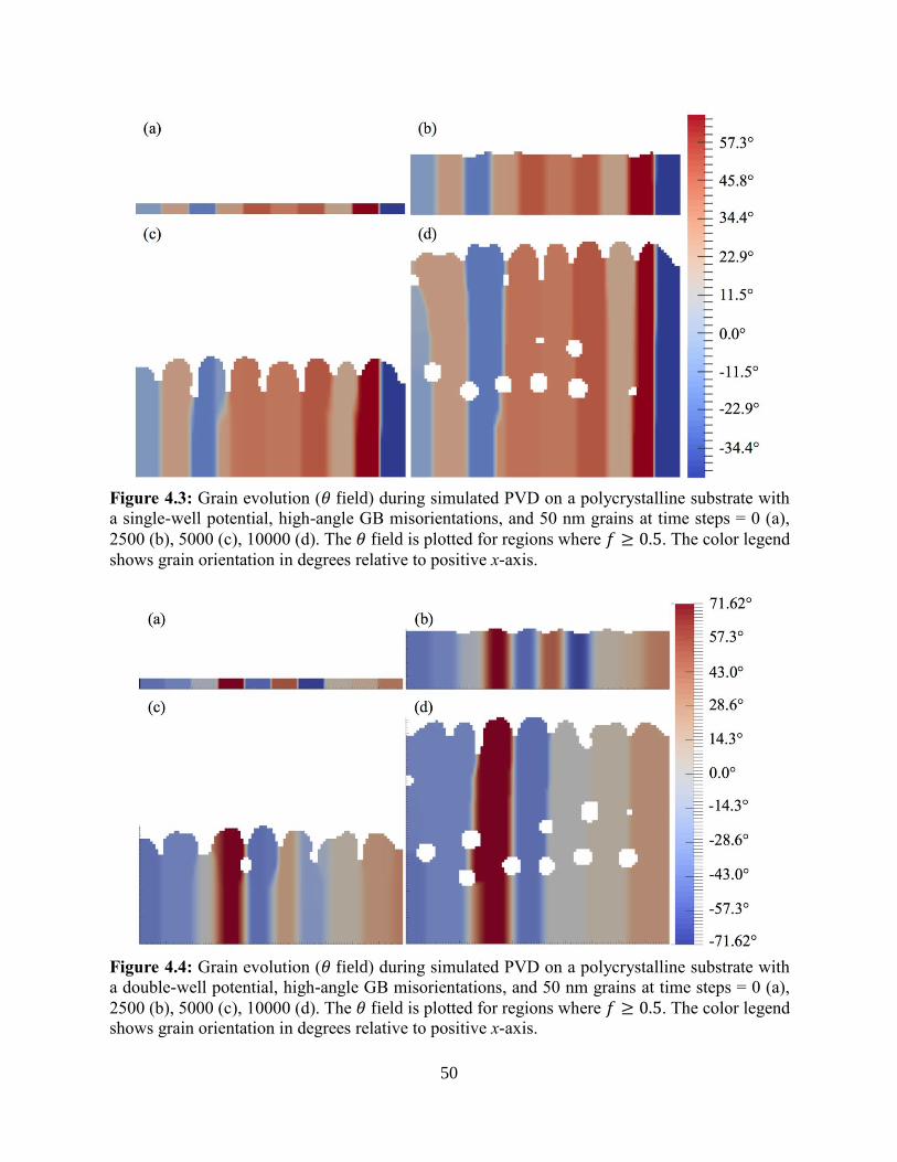
50
Figure 4.3: Grain evolution (𝜃 field) during simulated PVD on a polycrystalline substrate with
a single-well potential, high-angle GB misorientations, and 50 nm grains at time steps = 0 (a),
2500 (b), 5000 (c), 10000 (d). The 𝜃 field is plotted for regions where 𝑓 ≥ 0.5. The color legend
shows grain orientation in degrees relative to positive x-axis.
Figure 4.4: Grain evolution (𝜃 field) during simulated PVD on a polycrystalline substrate with
a double-well potential, high-angle GB misorientations, and 50 nm grains at time steps = 0 (a),
2500 (b), 5000 (c), 10000 (d). The 𝜃 field is plotted for regions where 𝑓 ≥ 0.5. The color legend
shows grain orientation in degrees relative to positive x-axis.

51
orientations. The observation of columnar structures containing unique and varying grain
orientations has been hypothesized [6,7,47,48] and observed experimentally in thin film oxides
[48,49], alloys [50], and aluminum [51]. Finally, comparing the simulation results for these four
cases, i.e., low-angle vs. high-angle and single-well vs. double-well, no dramatic differences are
observed in the evolution of the grains, GBs, influence of surface features, or the resulting
microstructure. The only difference is that most of the GBs created during PVD on a substrate
with low-angle GBs are thinner than the GBs created during PVD on a substrate with high-angle
GBs. As the misorientations increase, the GB thicknesses increase and are captured across
several mesh points. It should be noted that the choice of 𝜏𝜃 would influence these grain
evolution effects. For example, if 𝜏𝜃 is increased in magnitude, the grain evolution kinetics will
be reduced so that minimal grain rotation and GB migration occurs within the same simulation
time. On the other hand, if 𝜏𝜃 is reduced in magnitude, then grain rotation and GB migration will
occur at a significantly increased rate.
4.4 Effects of Varying Substrate Grain Sizes
In this section, a series of simulations are performed to investigate the role of substrate
grain size on the resulting microstructure of the PVD thin film. Since the PVD simulations in
Section 4.3 used a polycrystalline substrate with 50 nm grains, the PVD simulations in this
section are performed on an amorphous substrate and substrates with 25 nm, 100 nm, and 166.6
nm grains with high-angle GB misorientations. Simulation results are shown in Figures 4.5 -
4.12 for single-well and double-well potentials. The deposition flux rate in these PVD
simulations is again taken to be 𝐴𝑦 = −0.6.

52
Figure 4.5: Grain evolution (𝜃 field) during simulated PVD on an amorphous substrate (random
grain orientations) with a single-well potential at time steps = 0 (a), 2500 (b), 5000 (c), 10000
(d). The 𝜃 field is plotted for regions where 𝑓 ≥ 0.5. The color legend shows grain orientation
in degrees relative to positive x-axis.
Figure 4.6: Grain evolution (𝜃 field) during simulated PVD on an amorphous substrate (random
grain orientations) with a double-well potential at time steps = 0 (a), 2500 (b), 5000 (c), 10000
(d). The 𝜃 field is plotted for regions where 𝑓 ≥ 0.5. The color legend shows grain orientation
in degrees relative to positive x-axis.
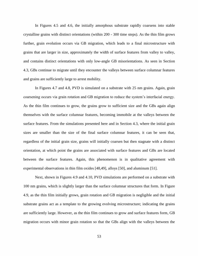
53
In Figures 4.5 and 4.6, the initially amorphous substrate rapidly coarsens into stable
crystalline grains with distinct orientations (within 200 - 300 time steps). As the thin film grows
further, grain evolution occurs via GB migration, which leads to a final microstructure with
grains that are larger in size, approximately the width of surface features from valley to valley,
and contains distinct orientations with only low-angle GB misorientations. As seen in Section
4.3, GBs continue to migrate until they encounter the valleys between surface columnar features
and grains are sufficiently large to arrest mobility.
In Figures 4.7 and 4.8, PVD is simulated on a substrate with 25 nm grains. Again, grain
coarsening occurs via grain rotation and GB migration to reduce the system’s interfacial energy.
As the thin film continues to grow, the grains grow to sufficient size and the GBs again align
themselves with the surface columnar features, becoming immobile at the valleys between the
surface features. From the simulations presented here and in Section 4.3, where the initial grain
sizes are smaller than the size of the final surface columnar features, it can be seen that,
regardless of the initial grain size, grains will initially coarsen but then stagnate with a distinct
orientation, at which point the grains are associated with surface features and GBs are located
between the surface features. Again, this phenomenon is in qualitative agreement with
experimental observations in thin film oxides [48,49], alloys [50], and aluminum [51].
Next, shown in Figures 4.9 and 4.10, PVD simulations are performed on a substrate with
100 nm grains, which is slightly larger than the surface columnar structures that form. In Figure
4.9, as the thin film initially grows, grain rotation and GB migration is negligible and the initial
substrate grains act as a template to the growing evolving microstructure; indicating the grains
are sufficiently large. However, as the thin film continues to grow and surface features form, GB
migration occurs with minor grain rotation so that the GBs align with the valleys between the

54
Figure 4.7: Grain evolution (𝜃 field) during simulated PVD on a polycrystalline substrate with
a single-well potential, high-angle GB misorientations, and 25 nm grains at time steps = 0 (a),
2500 (b), 5000 (c), 10000 (d). The 𝜃 field is plotted for regions where 𝑓 ≥ 0.5. The color legend
shows grain orientation in degrees relative to positive x-axis.
Figure 4.8: Grain evolution (𝜃 field) during simulated PVD on a polycrystalline substrate with
a double-well potential, high-angle GB misorientations, and 25 nm grains at time steps = 0 (a),
2500 (b), 5000 (c), 10000 (d). The 𝜃 field is plotted for regions where 𝑓 ≥ 0.5. The color legend
shows grain orientation in degrees relative to positive x-axis.
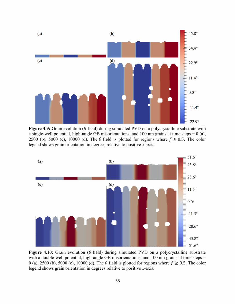
55
Figure 4.9: Grain evolution (𝜃 field) during simulated PVD on a polycrystalline substrate with
a single-well potential, high-angle GB misorientations, and 100 nm grains at time steps = 0 (a),
2500 (b), 5000 (c), 10000 (d). The 𝜃 field is plotted for regions where 𝑓 ≥ 0.5. The color
legend shows grain orientation in degrees relative to positive x-axis.
Figure 4.10: Grain evolution (𝜃 field) during simulated PVD on a polycrystalline substrate
with a double-well potential, high-angle GB misorientations, and 100 nm grains at time steps =
0 (a), 2500 (b), 5000 (c), 10000 (d). The 𝜃 field is plotted for regions where 𝑓 ≥ 0.5. The color
legend shows grain orientation in degrees relative to positive x-axis.

56
surface features. Furthermore, the presence of a GB at the peak of a surface feature causes the
formation of a new grain and GBs within the microstructure. In Figure 4.10, the initial substrate
grains again act as a template to the evolving microstructure with minimal grain rotation and GB
migration but with a wider GB thickness. As the thin film continues to grow and surface features
form, not only does grain rotation and GB migration occur but a subdivision of the existing
grains occurs, thus leading to several new GBs and smaller grains with distinct orientations that
differ from the parent grains. Furthermore, these newly created GBs are located at the valleys
between the columnar structures that form within a grain. These results reinforce the
observations discussed in Section 4.3 that the presence of a surface feature, such as a columnar
structure, influences the dynamics of grain coarsening during microstructure evolution
Finally, the last set of simulations shown in Figures 4.11 and 4.12, illustrate PVD on
substrates with 166.6 nm grains, which is significantly larger than the columnar features that
form. In Figure 4.11, the initial substrate grains act as a template for the growing microstructure
even with continued growth containing surface features. One of the GBs aligns with a valley
between columnar features while the other GB is initially located at a peak of a columnar feature.
The presence and evolution of this GB within the columnar feature leads to the formation of a
new and smaller grain that is uniquely associated with the surface feature. In Figure 4.12, the
initial substrate grains again act as a template for the growing microstructure with negligible
grain rotation and GB migration even in the presence of surface features. However, this is
expected since the GBs are initially fortuitously located near the formation of the valleys
between surface features. Furthermore, subdivision of the existing grains does not occur in either
case, indicating that the grains are large enough to prevent such events.
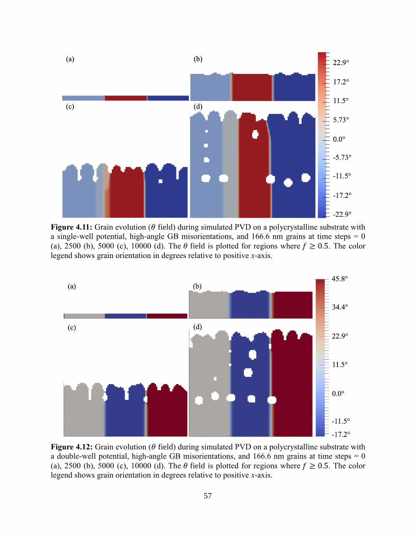
57
Figure 4.11: Grain evolution (𝜃 field) during simulated PVD on a polycrystalline substrate with
a single-well potential, high-angle GB misorientations, and 166.6 nm grains at time steps = 0
(a), 2500 (b), 5000 (c), 10000 (d). The 𝜃 field is plotted for regions where 𝑓 ≥ 0.5. The color
legend shows grain orientation in degrees relative to positive x-axis.
Figure 4.12: Grain evolution (𝜃 field) during simulated PVD on a polycrystalline substrate with
a double-well potential, high-angle GB misorientations, and 166.6 nm grains at time steps = 0
(a), 2500 (b), 5000 (c), 10000 (d). The 𝜃 field is plotted for regions where 𝑓 ≥ 0.5. The color
legend shows grain orientation in degrees relative to positive x-axis.
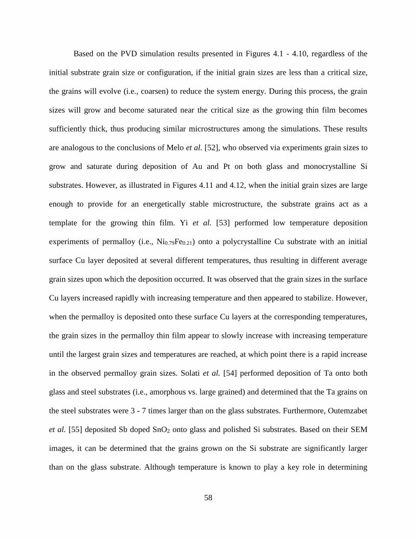
58
Based on the PVD simulation results presented in Figures 4.1 - 4.10, regardless of the
initial substrate grain size or configuration, if the initial grain sizes are less than a critical size,
the grains will evolve (i.e., coarsen) to reduce the system energy. During this process, the grain
sizes will grow and become saturated near the critical size as the growing thin film becomes
sufficiently thick, thus producing similar microstructures among the simulations. These results
are analogous to the conclusions of Melo et al. [52], who observed via experiments grain sizes to
grow and saturate during deposition of Au and Pt on both glass and monocrystalline Si
substrates. However, as illustrated in Figures 4.11 and 4.12, when the initial grain sizes are large
enough to provide for an energetically stable microstructure, the substrate grains act as a
template for the growing thin film. Yi et al. [53] performed low temperature deposition
experiments of permalloy (i.e., Ni0.79Fe0.21) onto a polycrystalline Cu substrate with an initial
surface Cu layer deposited at several different temperatures, thus resulting in different average
grain sizes upon which the deposition occurred. It was observed that the grain sizes in the surface
Cu layers increased rapidly with increasing temperature and then appeared to stabilize. However,
when the permalloy is deposited onto these surface Cu layers at the corresponding temperatures,
the grain sizes in the permalloy thin film appear to slowly increase with increasing temperature
until the largest grain sizes and temperatures are reached, at which point there is a rapid increase
in the observed permalloy grain sizes. Solati et al. [54] performed deposition of Ta onto both
glass and steel substrates (i.e., amorphous vs. large grained) and determined that the Ta grains on
the steel substrates were 3 - 7 times larger than on the glass substrates. Furthermore, Outemzabet
et al. [55] deposited Sb doped SnO2 onto glass and polished Si substrates. Based on their SEM
images, it can be determined that the grains grown on the Si substrate are significantly larger
than on the glass substrate. Although temperature is known to play a key role in determining

59
grain sizes during deposition (cf. [6,7,49,51,56,57]), the observations provided by Yi et al. [53],
Solati et al. [54], and Outemzabet et al. [55] indicate that as substrate grain sizes increase so does
the influence they contribute to the growing microstructure, as illustrated in Figures 4.11 and
4.12. It should be noted that the temperature dependencies were not considered in this research.
4.5 Flux Rate Effects on Microstructure Evolution
In this section, PVD simulations are performed with comparatively low and high incident
vapor flux rates, relative to Sections 4.3 and 4.4, to illustrate the effect of vapor flux rate on the
evolution of the thin film microstructure. The results of these simulations are illustrated in
Figures 4.13 - 4.16. The initial substrate microstructure considered in these simulations contains
10 high-angle GB misorientations that are 50 nm in size, as in Section 4.3.
To simulate low flux PVD, the incident vapor flux rate is taken to be 𝐴𝑦 = −0.16, which
is approximately 1 4⁄ of the flux rate in Sections 4.3 and 4.4. As a result, in Figures 4.13 and
4.14, it is observed that thin film solid growth occurs at a significantly reduced rate. With this
reduced flux rate, any vapor that is available at the surface is completely converted into solid
before additional vapor arrives. Furthermore, surface diffusion has an increased influence, as it is
able to reposition material along the thin film surface, thereby reducing the roughness of the
surface features although the individual peaks are more pronounced. The combination of these
processes results in the formation of a dense thin film with no underlying porosity, such as that
observed in Figures 4.1 - 4.12. The increase in deposition time required to grow the thin film
allows for further evolution of the underlying grains. In Figure 4.13 (c) and (d), it is observed
that this increase in deposition time and the smoothing of surface features leads to uniform
internal grain orientations and the GBs no longer prefer to position themselves only at the valleys

60
Figure 4.13: Phase (top) and grain (bottom) evolution during simulated low flux-rate PVD with
a single-well potential, high-angle GB misorientations, and 50 nm grains at time steps = 1000
(a) & (c), and 35000 (b) & (d). The top color legend indicates local density while the bottom
legend shows grain orientation in degrees relative to the positive x-axis.
Figure 4.14: Phase (top) and grain (bottom) evolution during simulated low flux-rate PVD with
a double-well potential, high-angle GB misorientations, and 50 nm grains at time steps = 1000
(a) & (c), and 35000 (b) & (d). The top color legend indicates local density while the bottom
legend shows grain orientation in degrees relative to the positive x-axis.

61
between surface features. In Figure 4.14 (c) and (d), different observations are made with regard
to grain evolution. Here, the increased deposition time leads to the formation of mostly larger
grains within the microstructure where the GBs stagnate at the valleys between only the largest
surface features. Based on the observations here and in Sections 4.3 and 4.4, there is indication
that the surface features must have sufficient size or roughness to influence grain and GB
evolution.
To simulate high flux PVD, the incident vapor flux rate is increased to 𝐴𝑦 = −2.5, which
is approximately 4 time the flux rate in Sections 4.3 and 4.4. As a result, in Figures 4.15 and
4.16, it is observed that thin film solid growth occurs at a significantly increased rate. Here, the
flux rate is large enough to prevent all available vapor at the surface from being completely
converted to solid before additional vapor arrives, reducing the importance of surface diffusion
effects. The combination of these processes results in the formation of a less dense thin film with
an underlying dendritic style microstructure. The decrease in deposition time required to growth
the thin film provides less time for the underlying grains to evolve. In Figures 4.15 and 4.16, the
grains coarsen to produce relatively uniform grain sizes within the final microstructure, which is
similar to the results presented in Figures 4.1 - 4.12, although there is more variation within the
grain orientations presented here. Furthermore, the grains sizes appear to be larger in Figure 4.16
(d) than in Figure 4.15 (d). The GBs beneath the thin film surface in many cases attempt to
follow and align with the regions of low phase-density that is characteristic of dendritic growth
and do not necessarily align with the valleys between surface features. The combination of these
phase and grain growth observations indicates that increased flux rates do not provide adequate
time for the underlying microstructure to fully relax to an energetically stable state. Although not
shown here, it should be noted that the field variable describing PVD in Figure 4.1 - 4.12
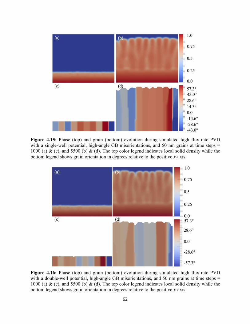
62
Figure 4.15: Phase (top) and grain (bottom) evolution during simulated high flux-rate PVD
with a single-well potential, high-angle GB misorientations, and 50 nm grains at time steps =
1000 (a) & (c), and 5500 (b) & (d). The top color legend indicates local solid density while the
bottom legend shows grain orientation in degrees relative to the positive x-axis.
Figure 4.16: Phase (top) and grain (bottom) evolution during simulated high flux-rate PVD
with a double-well potential, high-angle GB misorientations, and 50 nm grains at time steps =
1000 (a) & (c), and 5500 (b) & (d). The top color legend indicates local solid density while the
bottom legend shows grain orientation in degrees relative to the positive x-axis.

63
produces a dense thin film with pronounced columnar surface features and subsurface porosity,
which is reasonably captured in the corresponding grain orientation figures presented.
The results in this section are analogous to Monte Carlo simulations of nickel PVD
performed by Yang et al. [58] who observed the formation of thin films with columnar structures
containing distinct voids between structures at high deposition rates. At low deposition rates, thin
films with no underlying morphology with some surface roughness and large grains were
observed. Similar observations have been made experimentally. For example, Wolfe et al. [59]
performed deposition of TiN on steel substrates to study the role of various deposition
conditions. At the higher deposition rates, it was observed that thin films containing voids and
porosity (i.e., less dense) were formed; whereas at lower deposition rates, the density of the thin
film increased resulting in the porosity / voids being significantly reduced with slightly larger
grains.
4.6 Summary and Concluding Remarks
In this chapter, a “first treatment” phase-field model is developed and utilized that
couples previous models describing PVD and polycrystalline evolution in a sequential approach
allowing the simulation of thin film growth and subsurface grain evolution in a simplified
metallic system. To illustrate the utility and capability of this approach in capturing solid growth
and subsurface grain and GB evolution, this model is used to simulate PVD of a generic single-
phase polycrystalline metal with isotropic growth kinetics, and single-well and double-well
potentials. Specifically, this phase-field modeling approach is used to investigate (i) low-angle
and high-angle GB misorientation influences in a polycrystalline substrate, (ii) grain size
influences in a polycrystalline substrate, and (iii) flux rate influences on the evolving thin film
64
microstructure. It is important to note several limitations of this unidirectional coupling
approach, which are assumed for the sake of simplicity. First, PVD may result in metastable
phase formation and preferred growth directions or anisotropies (cf. [9,49]), which are neglected
in this initial treatment. Second, differences in attachment kinetics between the vapor phase and
the different orientations of the thin film surface and GBs, which can influence surface diffusion
and growth dynamics, are also neglected. More specifically, the surface features and subsurface
porosity predicted by the PVD model are capable of influencing microstructure evolution, but the
microstructure features such as local domain orientation or GB presence cannot influence surface
growth processes. Finally, the numerical parameters for the PVD model are constructed to be
non-dimensional whereas the grain evolution parameters have been related to physical quantities
to make the model more quantitative.
Regardless of the above limitations, a series of qualitative observations can be made
regarding the connection between surface morphology and subsurface evolution during PVD that
have experimental justification as discussed in previous sections. First, it is observed that there
are no significant differences in the evolution of grains and GBs or the resulting microstructures
between low-angle and high-angle misorientation substrates with either single-well or double-
well potentials. In these simulations, grains evolve through grain rotation and GB migration until
the grains reach sufficient size. Furthermore, GBs become immobilized at the valleys between
columnar structures. Next, it is observed that, regardless of initial grain size, grains evolve until
they become sufficiently large and growth stagnates, provided that the initial grain sizes are
below some critical size. When the initial grains are sufficiently large, the grains act as a
template for the growing thin film. Additionally, in some situations the surface columnar
structures may influence the subsurface microstructure to induce subdivision of grains; thus
65
forming additional grains and GBs. Finally, the influence of vapor flux rates on thin film
morphology is illustrated. At a low flux rate (𝐴𝑦 = −0.16), a fully dense thin film containing
some surface roughness and no subsurface features is formed. Additional deposition time
allowed for further grain evolution resulting in mostly uniform grain sizes or a mixture of
smaller and mostly larger grains, depending on the potential used. At an increased flux rate
(𝐴𝑦 = −0.6), a dense thin film containing distinct columnar structures and subsurface porosity is
formed. At an even larger flux rate (𝐴𝑦 = −2.5), a less dense thin film with surface roughness
and subsurface features resembling dendrites is formed. The decreased deposition time forces
minimal subsurface grain evolution; thus sufficient minimization of the microstructure is
prevented.
Finally, the absence of dramatic differences in the microstructure evolutions between the
single well and double-well potentials should be expected. Recall that microstructure evolution
via the polycrystalline model was only allowed to occur within the regions that were defined to
be the solid phase from the PVD model. Therefore, when using the double well potential,
evolution of the microstructure is biased towards the solid phase portion of the double well,
effectively becoming a single-well potential (recall Figure 2.2). However, differences in the
parabolic shape of the solid portion of the double well potential, which has a thermodynamic
dependence, and the single-well potential may lead to differences in predicting microstructure
evolution. Thus, the single-well potential is sufficient to describe grain evolution within a
polycrystalline microstructure using this sequentially coupled approach.

66
Chapter 5: Phase-Field Simulations of Physical Vapor Deposition and Microstructure
Evolution of a Two-Phase Metal
5.1 Introduction
This chapter presents two- and three-dimensional simulation results for physical vapor
deposition (PVD) of a pure allotropic metal with two stable solid phase and isotropic growth
kinetics using: the PVD and multiphase phase-field models described in Sections 2.2 and 2.4,
respectively, the phase nucleation approach described in Section 2.5, and the sequential coupling
method described in Section 3.3. First, Section 5.2 outlines the numerical methods implemented
to solve the equations of motion, construction of the initial system configurations, and the model
parameters used for PVD, multiple metallic phases, and phase nucleation. Next, Section 5.3.1
presents high temperature (i.e., above the phase transition temperature) PVD simulation results
performed on amorphous and polycrystalline substrates with comparatively low and high
interface mobilities. Section 5.3.2 presents simulation results for low temperature (i.e., below the
67
phase transition temperature) PVD of a high temperature phase on a single crystal substrate.
Section 5.3.3 presents simulation results on amorphous and polycrystalline substrate using a
Gaussian temperature distribution. Finally, Section 5.4 extends the multiphase PVD model to
three dimensions and presents simulation results illustrating surface morphology formation with
varying incident vapor flux rates.
5.2 Simulation Methodology and Model Parameters
The equations of motion described in Equations 2.5, 2.6, 2.14, and 2.16 are discretized
and solved on a uniform 100 x 350 mesh using the explicit first-order Euler method (Equation
3.4) for time and the centered second-order finite difference (Equation 3.6) approximation for
space. For all of these equations of motion, periodic boundary conditions are applied in the
directions parallel to the substrate (x-axis) while fixed boundary conditions (i.e., the values of the
solution are defined) are applied in the directions perpendicular to the substrate (y-axis), i.e., the
direction of growth.
In this research, the initial system configuration is that of a flat substrate parallel to and
spanning the x-axis, where 𝑓(𝒓, 0) = 1 and g(𝒓, 0) = 0 . Below the 𝑦 = 1 boundary, this
condition is held constant to provide a fixed substrate. The region above the substrate is taken to
be the vacuum region containing the incident vapor flux, where 𝑓(𝒓, 0) = −1 and g(𝒓, 0) = g0.
Beyond the 𝑦 = 350 boundary, these conditions are held fixed to provide a continuous source of
vapor flux during deposition. Within the initial substrate region (i.e., below 𝑦 = 1) a phase
distribution is constructed and held fixed, where 𝑝1(𝒓, 0) = 0 and the values of 𝑝𝑖(𝒓, 0), for 𝑖 =
2 − 𝑁, depend on the volume fraction ascribed to each phase at each mesh point. Furthermore,
within the initial vacuum region, only vapor exists so 𝑝1(𝒓, 0) = 1 and 𝑝𝑖(𝒓, 0) = 0, for 𝑖 = 2 −

68
𝑁. Finally, a temperature distribution is defined for the entire system within the substrate and
vapor regions. Within the substrate and above the 𝑦 = 350 boundary, this temperature
distribution is held fixed. Taking the temperature to be fixed at these boundaries and choosing
the y-axis to be larger than the x-axis allowed for heat released during deposition to diffuse into
and away from the thin film and eventually be removed so that large temperature build-ups are
prevented (i.e., the substrate and thin film are not thermally isolated from the surrounding
environment), which would occur in a closed system and artificially influence the
thermodynamics of phase evolution. Furthermore, if the y-axis is taken too small then heat will
artificially and rapidly be pulled away from the system leading to lower final temperature
distributions. The choice of domain size used in this research was determined by performing a
series of test simulations with sizes ranging between 100 x 100 and 100 x 500 mesh points that
focused on the temperature distribution of the system and calculated the average temperature at
𝑦 = 100 during each simulation as the thin film features are fully formed and evolve within the
Figure 5.1: Test PVD simulations for varying domain sizes illustrating the average temperature
value and evolution at 𝑦 = 100.

69
first 100 y-axis mesh points; these results are illustrated in Figure 5.1. Additionally, all PVD
simulation results are presented on the corresponding 100 x 100 domain. From these test
simulations, it was determined that a domain size of 100 x 350 mesh points provided a
reasonable treatment of temperature evolution, i.e., minor temperature differences were observed
within the thin film with domains above 100 x 350 mesh points, while still only requiring a
reasonable amount of computing time. Although not studied in detail in this research, it is
interesting to note the presence of a distinct change in the rate of temperature increase within
each simulation, which corresponds to the formation of surface features and subsurface porosity.
The non-dimensional PVD parameters in Equations 2.5 and 2.6 are chosen to produce
porous and columnar features during simulated of purely vertical PVD providing realistic
features to the thin film; these parameter values are summarized below in Table 5.1.
Parameter 𝑎 𝑏 𝐴𝑦 𝐵 𝐶 𝐷 g0
Value 0.5 -0.8 -0.6 10 2.5 0.01 1
Table 5.1: Non-dimensional parameters used to simulate columnar and porous growth during
purely vertical PVD.
The direction of growth is taken to be 𝑨 = 𝐴𝑦�̂�. The aggregation coefficient, 𝐵, is chosen to be
large enough to convert essentially all incident vapor into solid at the thin film surface. The noise
coefficient, 𝐶, is chosen to provide sufficient noise at the surface to allow surface features to
form but not large enough to dominate growth, which is then turned off after 100,000 time steps.
The diffusion coefficient, 𝐷, is chosen to be an order of magnitude smaller than A so that the

70
primary source of vapor transport is the flux parameter, 𝑨 [16]. The choice of the flux strength
parameters, 𝐴𝑦, was made so that a continuous supply of vapor arrives at the thin film surface
but does not lead to a build-up of unconverted vapor above the surface. Finally, the non-
dimensional spatial discretization is taken to be 1 as in Keblinski et al. [16] while the non-
dimensional temporal discretization is taken to be 10−5.
The physical quantities 𝐿𝑖𝑘, 𝜆𝑖𝑘, 𝑇𝑖𝑘, 𝜇𝑖𝑘, 𝜎𝑖𝑘 for multiphase evolution in Equation 2.14
and 𝜌𝑖, 𝐶𝑃, 𝑘𝑇, 𝐿𝑖𝑘 for temperature evolution in Equation 2.16 need to be defined for each phase
and combination of phases. The values used in this research for multiphase evolution are
summarized in Table 5.2 and represent reasonable values for an allotropic metal with two stable
phases, α and β, where α is the stable phase below the phase transition temperature and β is the
stable phase above the transition temperature.
Parameter 𝐿𝑖𝑘 (J cm3⁄ ) 𝜆𝑖𝑘 (cm) 𝑇𝑖𝑘(𝐾) 𝜎𝑖𝑘 (J cm2⁄ ) 𝜇𝑖𝑘 (cm/s∙K)
α - β 3.15 ∙ 102 5 ∙ 10−5 1200 5.175 ∙ 10−6 -
α - Vapor 4.0 ∙ 104 5 ∙ 10−5 3500 1.5 ∙ 10−5 10−6
β - Vapor 4.0 ∙ 104 5 ∙ 10−5 3500 1.95 ∙ 10−5 10−6
Table 5.2: Physical parameters for a two-phase metallic system used to simulate multiphase
evolution during PVD.
The values of parameters used in this research for multiphase evolution and phase nucleation
were motivated by Ti as physical data is readily available [60,61] and experimental PVD
observations have highlighted concurrent deposition and growth of α-Ti and β-Ti as a function
of temperature [9]; however, it should be noted that this model is not limited to just this material.
71
For simplicity, the interfacial energies and mobilities are taken to be constant. Furthermore,
𝐿𝑘𝑖 = −𝐿𝑖𝑘 and 𝜇𝑘𝑖 = −𝜇𝑖𝑘 depending on the direction of the phase transformation [24]. The
remaining quantities for temperature evolution are taken to be constant for all phases and are
chosen as: 𝜌𝑖 = 4.5 g cm3⁄ , 𝐶𝑃 = 0.5 J g ∙ K⁄ , and 𝑘𝑇 = 0.3 W cm ∙ K⁄ . For both Equations 2.14
and 2.16, the spatial and temporal discretizations are taken to be 10−5 cm and 10−11 ,
respectively, which corresponds to a physical domain size of 10 μm x 10 μm. To determine an
appropriate spatial discretization for these simulations, values between 10 nm - 1,000 nm were
used to determine sufficient phase evolution within the PVD simulation domain size and time
using an interface thickness of 𝜆 = 5 ∙ 𝑑𝑥.
The nucleation rate in Equation 2.17 has several quantities that require definition.
However, in this research, this expression is first simplified to reduce the complexity and number
of unique parameters. The parameters 𝛽 and (∆𝐺𝑛𝑢𝑐)2, both of which are temperature dependent
[26,29,30], and 𝐴3
2⁄ are combined into a single parameter, 𝛽∗ , giving Equation 5.1 for the
nucleation rate used in this research.
𝐽 =3
4√𝜋𝑘𝐵𝑇(𝜎𝑖𝑘)3
2⁄𝑁𝛽∗𝑒
(−∆𝐺∗
𝑘𝐵𝑇) (Equation 5.1)
where 𝛽∗ = 𝛽(∆𝐺𝑛𝑢𝑐)2 (𝐴)3
2⁄⁄ becomes a temperature-dependent numerical frequency factor
that controls that amplitude of the nucleation rate and, therefore, the number of nuclei to be
introduced. The value of 𝛽∗ is chosen to achieve production of multiple nuclei during the
simulations and is taken to be 𝛽∗ = 0.25 ∙ 10−35 for each simulation presented in this research.
However, in principle, this value should change with changing temperature, as its components

72
are temperature dependent. The number of atoms in each local phase-field volume, 𝑁 , is
assumed to be constant and taken to be 𝑁 = 2.0 ∙ 105; an approximation based on the volume of
a phase-field cell and the number of atoms per β-Ti unit cell. To determine the energy barrier
required to form a stable nucleus, ∆𝐺∗, and the free energy change per phase-field volume, ∆𝐺𝑉,
the free energies, 𝐺𝑉𝑖 , for each phase are required, which are also temperature dependent. In this
research, the free energies for the α and β phases are approximated as linear functions of
temperature and are chosen as: 𝐺𝑉𝛼 = 0.025𝑇 + 14.0 J/mol ∙ K and 𝐺𝑉
β= 0.015𝑇 + 26.0 J/mol ∙
K , where these functions intersect at 𝑇 = 1200 K (i.e., the solid state transformation
temperature). These functions are motivated by the temperature dependence of the free energies
for Ti [61]; however, the free energy values and slopes of these relationships are modified to
amplify the difference in free energies as the temperature deviates from the transition
temperature. Below the phase transition temperature, the free energy for the α-phase is lower
Figure 5.2: Nucleation probability profiles using Equation 5.1 and the physical parameters
and relationships motivated by two-phase Ti.

73
than for the β phase, thus providing a higher probability of α nuclei production within the β-
phase while a smaller probability is calculated for β phase production within the α -phase.
Opposite arguments can be made for free energies and nucleation probabilities above the phase
transition temperature. Figure 5.2 illustrates nucleation probabilitues for this two-phase system
using Equation 5.1 and the physical parameters and realtionships discussed above.
5.3 Two-Dimensional Simulation Results and Discussion
5.3.1 Low vs. High Interface Mobility Effects
Using the modeling approach described in Sections 3.3 and 5.2, PVD simulations are
performed on an amorphous substrate, where a random solid phase is specified at each phase-
field volume within the substrate, and a bicrystal substrate, where the substrate is equally divided
into α and β regions. Two different values for the α-β interface mobility are selected for these
simulations as 0.0035 cm s ∙ K⁄ and 0.035 cm s ∙ K⁄ , which are reasonable values for a pure
metal based on molecular dynamics simulations [62,62]. Simulation results using combinations
of these substrates and interface mobilities are illustrated in Figures 5.3 - 5.6.
First, PVD simulation results with a α-β interface mobility of 0.0035 cm s ∙ K⁄ and a
deposition temperature of 𝑇 = 1350 K, which is above the α-β transition temperature, are shown
in Figure 5.3 for an amorphous substrate and Figure 5.4 for a bicrystal substrate. During the
initial stages of solid growth in both simulations, the phase distribution of the substrate acts as a
template for the phase distribution of the growing thin film and the phases grow vertically with
approximately the same rate. However, as solid growth continues, the existing metastable α-
phase (grey) within the thin films begin to transition into the stable β-phase (red), beginning near
the thin film surface. In Figure 5.3, the transition to a β-phase dominant thin film occurs more

74
Figure 5.3: Simulated PVD on an amorphous substrate with 𝜇 = 0.0035 cm s ∙ K⁄ , 𝑇 = 1350 K
and 𝛽∗ = 0.25 ∙ 10−35at time steps (a) 0, (b) 2500000, (c) 6250000, and (d) 12500000. The
phase with the maximum local volume fraction is plotted. (e) Global volume fraction evolution
of each phase during the PVD simulation. The constant volume fraction of the substrate is
included in this calculation to provide a consistent description with the images on the left.
Figure 5.4: Simulated PVD on a bicrystal substrate with 𝜇 = 0.0035 cm s ∙ K⁄ , 𝑇 = 1350 K
and 𝛽∗ = 0.25 ∙ 10−35 at time steps (a) 0, (b) 2500000, (c) 7500000, and (d) 12500000. The
phase with the maximum local volume fraction is plotted. (e) Global volume fraction evolution
of each phase during the PVD simulation. The constant volume fraction of the substrate is
included in this calculation to provide a consistent description with the images on the left.

75
rapidly due to the amorphous nature of the substrate with many β-phase regions in relatively
close proximity. Additionally, as the upper portion of the thin film becomes dominated by the β-
phase, further deposition and growth of the α-phase becomes unfavorable. In Figure 5.4, the
metastable α-phase region in much larger and is therefore able to exist at larger film thicknesses.
As the thin film grows in both simulations, the initially uniform temperature distribution, which
is held fixed at the substrate, develops a gradient within the thin film due to the release of latent
heat at the deposition surface. During these simulations, the temperature of the thin film surface
becomes approximately 60% hotter than the substrate. It is worthwhile to note that if the
simulation domain size were taken as 100 x 100, the temperature of the thin film surface would
become approximately 20% hotter than the substrate during deposition and then reduce to
approximately 6% hotter than the substrate due to the fixed temperature boundary condition at
the top of the domain (recall Figure 5.1). Finally, it can be seen in Figures 5.3 and 5.4 that phase
nucleation mostly occurs near the substrate and decreases as the film increases in thickness. This
is due to the temperature gradient that forms with higher temperatures near the thin film surface,
which results in a decrease in the nucleation probability (recall Figure 5.2). These nuclei exhibit
minimal to no growth, even after many time steps after they are formed, which is due to the
small interface mobility value used. Moreover, the α-phase nuclei that form within the β-phase
do not grow and tend to rapidly dissolve.
Next, Figures 5.5 and 5.6 illustrate PVD simulation results with a α-β interface mobility
of 0.035 cm s ∙ K⁄ and a deposition temperature of 𝑇 = 1350 K, for amorphous and bicrystal
substrates, respectively. Again, during the initial stages of solid growth in both simulations, the
phase distribution of the substrate acts as a template for the phase distribution in the thin film and
the phases grow vertically. However, as opposed to the results shown in Figures 5.3 and 5.4, the
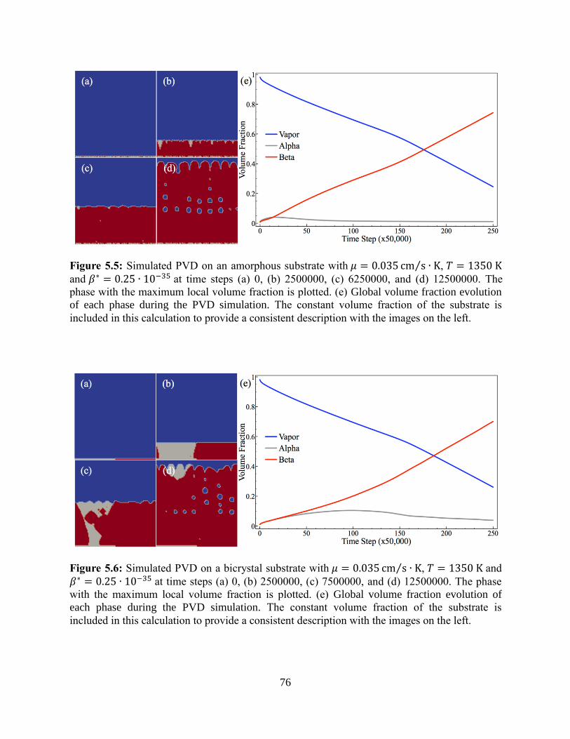
76
Figure 5.5: Simulated PVD on an amorphous substrate with 𝜇 = 0.035 cm s ∙ K⁄ , 𝑇 = 1350 K
and 𝛽∗ = 0.25 ∙ 10−35 at time steps (a) 0, (b) 2500000, (c) 6250000, and (d) 12500000. The
phase with the maximum local volume fraction is plotted. (e) Global volume fraction evolution
of each phase during the PVD simulation. The constant volume fraction of the substrate is
included in this calculation to provide a consistent description with the images on the left.
Figure 5.6: Simulated PVD on a bicrystal substrate with 𝜇 = 0.035 cm s ∙ K⁄ , 𝑇 = 1350 K and
𝛽∗ = 0.25 ∙ 10−35 at time steps (a) 0, (b) 2500000, (c) 7500000, and (d) 12500000. The phase
with the maximum local volume fraction is plotted. (e) Global volume fraction evolution of
each phase during the PVD simulation. The constant volume fraction of the substrate is
included in this calculation to provide a consistent description with the images on the left.

77
β-phase consumes the α-phase more rapidly with α-phase consumption originating near the
substrate and then propagating towards the thin film surface, which is due to the increased
interface mobility. In Figure 5.5, the close proximity of β-phase regions throughout the substrate
combined with the increased interface mobility allows for the thin film to rapidly transition to a
β-phase thin film with the exception of several α-phase nuclei. In Figure 5.5, the β-phase nuclei
introduced within the α-phase region are able to substantially grow and aid in consuming the α-
phase, which again is a result of the increased interface mobility. This effect also occurs in
Figure 5.5 although it is difficult to observe due to the rapid consumption of the slender α-phase
regions. The nuclei that form within the thin film mostly occur in the early stages of deposition
due to the temperature gradient generated by latent heat released during deposition. Based on
these simulations, it can be concluded that the phase distribution of the substrate used for
deposition, the interface mobility between material phases, and the temperature gradients
allowed to form within the thin film play a significant role in the resulting microstructure phase
distribution.
As a final observation, as the thin film grows, surface features and subsurface porosity
are predicted by the solution of Equations 2.5 and 2.6 for PVD. This roughness transition can be
identified in Figures 5.3 - 5.6 (e) identifying the global volume fraction evolution of each phase
within the domain as a change in the rate of consumption of the vapor phase. This increase in the
rate of vapor phase consumption is likely due to the increase in surface area of the thin film due
to the roughening transition. This observation is consistent for all simulations presented.

78
5.3.2 Low Temperature PVD of a High Temperature Phase
In this section, PVD simulations are performed with a purely β -phase substrate at
temperatures below the α-β transition temperature to model low temperature deposition of a high
temperature phase. These simulations are performed at 𝑇 = 900 K, shown in Figure 5.7, and 𝑇 =
1080 K , shown in Figure 5.8 (recall the phase transition temperature was defined as 𝑇 =
1200 K). The α-β interface mobility is taken to be 0.035 cm s ∙ K⁄ and the phase nucleation
coefficient is taken to be a constant as 𝛽∗ = 0.25 ∙ 10−35, which is known to be sensitive to
temperature changes and should in general change with temperature variations.
In both figures, it can be seen that there is initially growth of the β-phase, followed by the
formation of several α-phase nuclei, which in turn show substantial growth as it is the stable
phase below the α-β transition temperature. However, as growth continues the temperature
gradient of the thin film increases due to latent heat release during deposition and the α-β
transition temperature is approached and crossed, which occurs sooner in Figure 5.8 than in
Figure 5.7 due to the initial deposition temperature being closer to the α-β transition temperature.
Within this region, the nucleation probability rapidly increases as the α- and β-phases have free
energies that become closer together (recall Figure 5.2) and a very large number of α-phase
nuclei are formed leading to a band of stable α-phase within the thin film corresponding to the
region where the α-β transition temperature is located within the solid. For both simulations,
within the solid region above the α-β transition temperature, the stable phase is the β-phase and
continues to grow and with no α-phase nucleation. However, in the solid region below the α-β
transition temperature, the preexisting β-phase is consumed by the formation and growth of α-
phase nuclei, which is the stable phase in this temperature regime. Additional simulations (not
shown here) with varying values of 𝛽∗ indicate that the value of 𝛽∗ used in the above simulations

79
Figure 5.7: Simulated PVD on a 𝛽-phase substrate with 𝜇 = 0.035 cm s ∙ K⁄ , 𝑇 = 900 K and
𝛽∗ = 0.25 ∙ 10−35 at time steps (a) 0, (b) 3750000, (c) 7500000, and (d) 12500000. The phase
with the maximum local volume fraction is plotted. (e) Global volume fraction evolution of
each phase during the PVD simulation. The constant volume fraction of the substrate is
included in this calculation to provide a consistent description with the images on the left.
Figure 5.8: Simulated PVD on a 𝛽-phase substrate with 𝜇 = 0.035 cm s ∙ K⁄ , 𝑇 = 1080 K and
𝛽∗ = 0.25 ∙ 10−35 at time steps (a) 0, (b) 3750000, (c) 7500000, and (d) 12500000. The phase
with the maximum local volume fraction is plotted. (e) Global volume fraction evolution of
each phase during the PVD simulation. The constant volume fraction of the substrate is
included in this calculation to provide a consistent description with the images on the left.

80
may be too large for these temperature regimes and that smaller or temperature dependent values
of 𝛽∗ may be required, as the nucleation probability rapidly changes when the phase transition
temperature is approached (recall Figure 5.2). Smaller values of 𝛽∗ would reduce the number of
nuclei that are introduced to a reasonable amount and remove the sudden formation of an α-
phase region that spans the x-domain.
5.3.3 PVD on Substrates with a Temperature Distribution
In this section, PVD simulations are performed on amorphous and bicrystal substrates,
shown in Figures 5.9 and 5.10, using a temperature distribution that follows a Gaussian profile
where the middle of the system is taken to be 𝑇 = 1350 K and decreases horizontally outward to
𝑇 = 1000 K at the domain boundaries. These PVD simulations are experimentally motivated by
the work of Bunshah and Juntz [9], who showed that regions of stable α-Ti or β-Ti formation
were influenced by the presence of temperature gradients within the substrate. The α-β interface
mobility is taken to be 0.035 cm s ∙ K⁄ and the nucleation parameter is taken to be 𝛽∗ = 0.25 ∙
10−35.
In Figure 5.9, the amorphous substrate phase distribution initially acts as a template for
the phase distribution within the growing thin film. However, due to the proximity of slender α-
and β-phase regions throughout the thin film, the stable phases associated with each temperature
regime rapidly begin to coarsen. As thin film growth continues, the latent heat released during
the deposition process increases the temperature near the thin film surface to be sufficiently large
so that phase nucleation is reduced and the only stable phase in this region is the β-phase, which
subsequently becomes the only phase being deposited. As such, the remaining α-phase regions
exist at low temperature regions deep within the thin film near the substrate where the Gaussian

81
Figure 5.9: Simulated PVD on an amorphous substrate with 𝜇 = 0.035 cm s ∙ K⁄ , 𝛽∗ = 0.25 ∙10−35 and a temperature distribution that follows a Gaussian profile with 𝑇 = 1350 K in the
middle of the system and 𝑇 = 1000 K at the horizontal boundaries at time steps (a) 0, (b)
2500000, (c) 7500000, and (d) 12500000. The phase with the maximum local volume fraction is
plotted. (e) Global volume fraction evolution of each phase during the PVD simulation. The
constant volume fraction of the substrate is included in this calculation to provide a consistent
description with the images on the left.
Figure 5.10: Simulated PVD on a bicrystal substrate with 𝜇 = 0.035 cm s ∙ K⁄ , 𝛽∗ = 0.25 ∙10−35 and a temperature distribution that follows a Gaussian profile with 𝑇 = 1350 K at the
middle of the system and 𝑇 = 1000 K at the horizontal boundaries at time steps (a) 0, (b)
2500000, (c) 7500000, and (d) 12500000. The phase with the maximum local volume fraction is
plotted. (e) Global volume fraction evolution of each phase during the PVD simulation. The
constant volume fraction of the substrate is included in this calculation to provide a consistent
description with the images on the left.
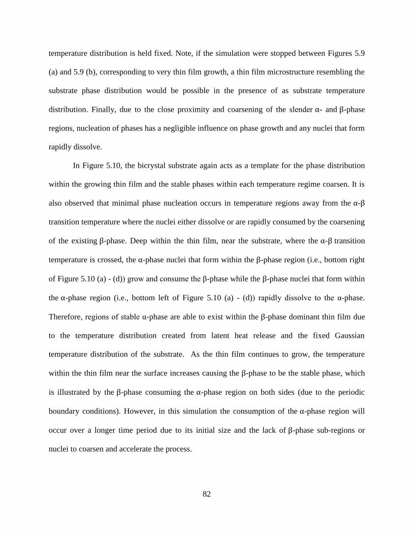
82
temperature distribution is held fixed. Note, if the simulation were stopped between Figures 5.9
(a) and 5.9 (b), corresponding to very thin film growth, a thin film microstructure resembling the
substrate phase distribution would be possible in the presence of as substrate temperature
distribution. Finally, due to the close proximity and coarsening of the slender α- and β-phase
regions, nucleation of phases has a negligible influence on phase growth and any nuclei that form
rapidly dissolve.
In Figure 5.10, the bicrystal substrate again acts as a template for the phase distribution
within the growing thin film and the stable phases within each temperature regime coarsen. It is
also observed that minimal phase nucleation occurs in temperature regions away from the α-β
transition temperature where the nuclei either dissolve or are rapidly consumed by the coarsening
of the existing β-phase. Deep within the thin film, near the substrate, where the α-β transition
temperature is crossed, the α-phase nuclei that form within the β-phase region (i.e., bottom right
of Figure 5.10 (a) - (d)) grow and consume the β-phase while the β-phase nuclei that form within
the α-phase region (i.e., bottom left of Figure 5.10 (a) - (d)) rapidly dissolve to the α-phase.
Therefore, regions of stable α-phase are able to exist within the β-phase dominant thin film due
to the temperature distribution created from latent heat release and the fixed Gaussian
temperature distribution of the substrate. As the thin film continues to grow, the temperature
within the thin film near the surface increases causing the β-phase to be the stable phase, which
is illustrated by the β-phase consuming the α-phase region on both sides (due to the periodic
boundary conditions). However, in this simulation the consumption of the α-phase region will
occur over a longer time period due to its initial size and the lack of β-phase sub-regions or
nuclei to coarsen and accelerate the process.

83
5.4 Three-Dimensional Simulation Results and Discussion
In this section, the two-dimensional multiphase PVD model is extended to three
dimensions and PVD simulations are performed with two different flux rates on a bicrystal
substrate to illustrate that the conclusions drawn using a simplified two-dimensional model are
valid in three-dimensions. The results of these PVD simulations are illustrated in Figures 5.11
and 5.12. The α-β interface mobility in these simulations is again chosen to be 0.035 cm s ∙ K⁄
while the deposition temperature is taken to be 𝑇 = 1350 K, which is above the α-β transition
temperature. Furthermore, to decrease computational demand, the simulation domain size is
taken to be 80 x 80 x 80 and the phase nucleation algorithm is turned off.
PVD simulation results with 𝐴𝑦 = −0.6 are illustrated in Figure 5.10 while results for
𝐴𝑦 = −2.5 are illustrated in Figure 5.11 where (a) illustrates the resulting microstructure, i.e.,
𝑓(𝒓, 𝑡) field, predicted by Equations 2.5 and 2.6, (b) illustrates the resulting multiphase evolution
within the thin film solid regions, and (c) illustrates the resulting temperature distribution due to
latent heat release. It should be noted that the cubic nature of the simulation domain and the fixed
temperature boundary condition at the top of the simulation domain causes heat to be pulled
away faster than the two-dimensional simulations in Section 5.3. In Figure 5.11, the formation of
columnar structures and subsurface porosity is observed. Additionally, any cross-section of these
three-dimensional simulations effectively corresponds to the two-dimensional simulations.
Within the solid regions, the initial bicrystal substrate leads to the growth of α- and β-phases.
However, as the deposition temperature is above the α-β transition temperature, the α-phase
transitions to the β-phase throughout the simulation and begins near the substrate. Similarly,
Figure 5.12 illustrates the formation of a less dense thin film with diffuse subsurface porosity
where the columnar features are thinner and more abundant than in Figure 5.11. Furthermore,

84
Figure 5.11: Simulated PVD on bicrystal substrate with 𝐴𝑦 = −0.6, 𝜇 = 0.035 cm s ∙ K⁄ and
𝑇 = 1350 K at time step 107 where (a) is the phase-field, (b) is the underlying multiphase field,
and (c) is the temperature field. All data is plotted for regions where 𝑓 ≥ 0.5.
Figure 5.12: Simulated PVD on a bicrystal substrate with 𝐴𝑦 = −2.5, 𝜇 = 0.035 cm s ∙ K⁄ and
𝑇 = 1350 K at time step 5 ∙ 106 where (a) is the phase-field, (b) is the underlying multiphase
field, and (c) is the temperature field All data is plotted for regions where 𝑓 ≥ 0.5.

85
with a higher incident vapor flux rate than Figure 5.11, there is less time for the α-phase to
transition to the stable β-phase during the simulation; leading to slower consumption of the α-
phase. Finally, Figures 5.11 (c) and 5.12 (c) illustrate the formation of a temperature gradient
within the solid as a result of latent heat release due to deposition where the surface of the thin
film becomes hotter than the regions of solid near the substrate, which leads to different phase
evolution kinetics in each region.
5.5 Summary and Concluding Remarks
In this chapter, a “first treatment” phase-field model is developed and utilized that
couples previous modeling efforts in a sequential approach to simulate thin film growth,
subsurface phase evolution, and phase nucleation in multiphase thin films. To illustrate this
model’s utility and capability in capturing these growth and evolution aspects, PVD simulations
are performed considering a generic allotropic metal with two stable solid phases and isotropic
growth kinetics. Specifically, this model is used to study the role of initial substrate phase
distribution and temperature on the resulting thin film microstructure by investigating (i)
interface mobility effects on phase growth, (ii) deposition of a high temperature phase below the
phase transition temperature, and (iii) temperature distribution effects on microstructure
evolution. It is important to note several limitations, which have been assumed in this first
treatment for simplicity. First, real materials have grain orientations and grain boundaries
associated with the phases present, which are neglected in this chapter - in theory, the orientation
methodology presented in Chapter 4 could be connected to the phase distribution here to create a
complete model. Furthermore, these grains may have preferred growth directions or anisotropies
that influence PVD growth dynamics, which are also neglected. Second, different attachment

86
kinetics between the vapor phase and the phases present at the thin film surface are also
neglected, which can also influence surface diffusion and growth dynamics [7,64]. Specific to
this work, the features developed by the PVD model are able to influence the phase evolution of
the underlying microstructure, but the underlying features are not able to influence surface
growth dynamics. Finally, the PVD equations of motion and parameters were constructed to be
non-dimensional whereas the multiphase and phase nucleation models can be linked to physical
quantities making them quantitative.
Regardless of the above limitations, the simulations results presented here allow several
qualitative observations to be made regarding the connection between substrate phase
distribution, temperature, and the resulting thin film microstructure. First, the substrate phase
distribution tends to act as a template to the depositing and growing phases within the thin film
until the thin film becomes sufficiently thick for the thermodynamics to control evolution.
However, it was also shown that the interface mobility affects the rate at which the stable phases
grow and the regions of the thin film where the phases tend to evolve (e.g., near the substrate or
near the surface). Next, as the thin film grows, latent heat is released at the thin film surface
causing a temperature gradient to form where the regions near the thin film surface increase to
become hotter than the substrate region. This temperature gradient causes the nucleation rate of
the phases to change throughout the thickness of the thin film, where the nucleation rate is
decreased in higher temperature regions, thus causing nucleation to occur mostly in the regions
away from the thin film surface or near the substrate. The value for the nucleation parameter, 𝛽∗,
needs to be carefully chosen as a function of temperature so that neither excessive nucleation nor
lack of nucleation occurs, depending on the material system. Finally, imposing a substrate
temperature distribution combines all of these observations in that there are temperature regions

87
within the thin film where different phases are stable and able to grow or nucleate whereas in
another region different phases may be stable and nucleation may or may not occur. Therefore,
the substrate phase distribution and temperature along with material specific quantities play a
significant role in the growth and underlying evolution of multiphase thin films as captured by
this model.

88
Chapter 6: Extending a Free Energy Functional for Physical Vapor Deposition to
Include Single-Phase Polycrystalline Materials
6.1 Introduction
This chapter proposes a novel free energy functional for modeling physical vapor
deposition (PVD) of a single-phase polycrystalline material in a physically consistent manner by
incorporating the appropriate dynamics for PVD and grain evolution from Chapter 2, where all
equations of motion can be derived from this single free-energy functional. Then PVD
simulations of a generic single-phase metal are performed using this novel approach to illustrate
the capabilities of this model in capturing concurrent solid growth and subsurface grain
evolution, which can be compared to the sequential coupling approach described in Section 3.2
with results in Chapter 4. First, Section 6.2 outlines the construction of this novel free energy
functional and the associated equations of motion. Next, Section 6.3 outlines the numerical
methods implemented to solve the equations of motion, construction of the initial system

89
configuration, and the model parameters used. Section 6.4 presents simulation results performed
for substrates with low-angle and high-angle grain boundary (GB) misorientations, substrates
with varying grain sizes, and polycrystalline substrates with low and high incident vapor flux
rates. Finally, Section 6.5 presents simulation results investigating the influence of the grain
evolution parameters 𝜏𝜃, 𝑠, and 휀 on the growing solid and microstructure.
6.2 Free Energy Functional and Equations of Motion
The novel PVD model developed in this research is a straightforward extension of the
Keblinski et al. [16] PVD model described in Section 2.2 by incorporating grain orientation and
GB effects in the manner proposed by Warren et al. [23] as discussed in Section 2.4. This
extension allows for the modeling and simulation of simultaneous solid growth, surface feature
formation, grain growth, and GB migration under PVD conditions, which is an improvement on
the sequential method developed in Section 3.2. Using the variables 𝑓(𝒓, 𝑡) and 𝜃(𝒓, 𝑡), this
extension is contained within the free energy functional shown below in Equation 6.1.
𝐹 = ∫ (−1
2𝑓2 +
1
4𝑓4 + 𝑎(𝛁𝑓)2 + 𝑠 (
𝑓 + 1
2)
2
|∇𝜃| +휀2
2(
𝑓 + 1
2)
2
|∇𝜃|2) 𝑑Ω (Equation 6.1)
As discussed in Sections 2.2 and 2.4, 𝑓(𝒓, 𝑡) ≈ 1 defines a solid region and 𝑓(𝒓, 𝑡) ≈ −1 defines
a region of vacuum or no solid while 𝜃(𝒓, 𝑡) describes the local grain orientation as measured
from a defined global axis (the positive x-axis in Warren et al. [23] and this research) and varies
between 0 and 2𝜋 𝑁𝑆⁄ , where 𝑁𝑆 is the rotational symmetry of the crystal. Furthermore, the grain
gradient coefficient functions (i.e., functions g and ℎ in Equation 2.7) are taken to be quadratic in

90
the local solid density 𝑓𝑑(𝒓, 𝑡) = (𝑓(𝒓, 𝑡) + 1) 2⁄ so that orientation effects are removed within
the disordered vapor region as there is no physical meaning of order within this region.
With this free energy functional containing variables to describe solid and grain
evolution, all equations of motion for PVD of a single-phase polycrystalline material can then be
determined. The complete set of equations used in this research is shown in Equations 6.2, 6.3,
and 6.4. Equations 6.2 and 6.3, which are the equations of motion proposed by Keblinski et al.
[16], are used here to describe all PVD growth processes for the solid phase. The inclusion of the
orientation parameter, 𝜃(𝒓, 𝑡), requires an additional equation of motion describing its evolution.
This is determined from Allen-Cahn dynamics (Equation 2.2) and gives rise to the grain equation
of motion in Equation 6.4.
𝜕𝑓
𝜕𝑡= 𝛁2
𝛿𝐹
𝛿𝑓+ 𝐵(𝛁𝑓)2g + 𝐶√(𝛁𝑓)2g𝜂 (Equation 6.2)
𝜕g
𝜕𝑡= 𝛁[𝐷𝛁g − 𝑨g] − 𝐵(𝛁𝑓)2g (Equation 6.3)
𝑃(|∇θ|)𝜏𝜃 (𝑓 + 1
2)
2 𝜕𝜃
𝜕𝑡= ∇ ∙ [(
𝑓 + 1
2)
2
(𝑠
|∇𝜃|+ 휀2) ∇𝜃] (Equation 6.4)
6.3 Simulation Methodology and Model Parameters
The equations of motion described in Equations 6.2, 6.3, and 6.4 are discretized and
solved on a uniform 100 x 100 square mesh. Equations 6.2 and 6.3 are solved using the explicit
first-order Euler method (Equation 3.4) and centered second-order finite difference (Equation
3.6) approximations for time and space, respectively. For both of these equations, no-flux
boundary conditions (i.e., the derivatives are taken to be zero) are applied in the direction parallel
to the substrate (x-axis) while anti-periodic boundary (i.e., the values of the solution are defined
91
and opposite in sign) conditions are applied perpendicular to the substrate (y-axis). Equation 6.4
is solved using a fully implicit approach where the method of conjugate gradients is implemented
to solve the associated system of equations. No-flux boundary conditions are also applied at each
boundary for this equation. The complete discretization of Equation 6.4 is given in detail in
Warren et al. [23].
In this research, the initial system configuration is that of a flat substrate parallel to and
spanning the x-axis with a thickness of 5 mesh points in the y-direction, where 𝑓(𝒓, 0) = 1 and
g(𝒓, 0) = 0. This condition is assumed to be constant below the 𝑦 = 1 boundary to provide a
fixed substrate region. Above the substrate is taken to be the vacuum region containing the
incident vapor flux, where 𝑓(𝒓, 0) = −1 and g(𝒓, 0) = g0. Beyond the 𝑦 = 100 boundary, this
condition is held fixed to provide a continuous source of vapor flux during deposition. Within the
initial substrate region, a polycrystalline microstructure is constructed, where 𝜙(𝒓, 0) = 1 and
𝜃(𝒓, 0) depends on the orientation ascribed to each grain within the region. Furthermore, within
the vacuum region, 𝜙(𝒓, 0) = 0 while 𝜃(𝒓, 0) can be any arbitrary value to allow Equation 6.4 to
be solved, as it has no physical meaning in this region. As such, in this research, the values of
𝜃(𝒓, 0) are randomly chosen from the interval (−𝜋, 𝜋) [23].
Model parameters that are fixed across all simulations in this chapter are presented here
while parameters that are varied are presented with the corresponding simulation results. The
equations of motion in Equations 6.2, 6.3, and 6.4 are assumed to be non-dimensional. As such,
the non-dimensional spatial and temporal discretizations for these equations are taken to be 1 and
0.01, respectively. These values, which follow from Keblinski et al. [16], were determined as
necessary to ensure numerical stability when solving Equations 6.2 and 6.3. The model
parameters controlling PVD in Equations 6.2 and 6.3 are chosen to produce porous and columnar
92
features during simulation of purely vertical PVD providing realistic features to the solid phase;
these parameters are summarized below in Table 6.1.
Parameter 𝑎 𝑏 𝐵 𝐶 𝐷 g0
Value 0.5 -0.8 10 2.5 0.01 1
Table 6.1: Non-dimensional parameters used to simulate columnar and porous growth during
purely vertical PVD.
As in Chapter 4, the direction of growth is taken to be 𝑨 = 𝐴𝑦�̂�. The aggregation coefficient, 𝐵,
is chosen to be large enough to convert essentially all incident vapor into solid at the interface.
The noise coefficient, 𝐶, is chosen to provide sufficient noise at the surface to allow surface
features to form but not large enough to dominate growth, which is then turned off after 1,000
time steps. The diffusion coefficient, 𝐷, is chosen to be an order of magnitude smaller than 𝑨 so
that the primary source of vapor transport is the flux parameter, 𝑨 [16]. Finally, the density of the
initial vapor field, g0, is taken to be 1.
Since the model parameters, 𝑠 and 휀 , controlling grain evolution in Equation 6.4 are
assumed to be non-dimensional, they are taken to have the same values as determined in Chapter
4, even though these values were derived from relationships to physical quantities: 휀 = 0.0141
and 𝑠 = 0.0176 . Furthermore, the non-dimensional parameters controlling the rate of grain
growth and grain evolution kinetics are taken to be 𝜏𝜃 = 10−1, 𝜇 = 103, and 𝛽 = 105. It should
be noted that the value of 𝜏𝜃 here is an order of magnitude smaller than in Chapter 4, thus
leading to faster grain kinetics, which is necessary to observe reasonable and comparable grain
93
evolution as in Chapter 4. The values of these grain evolution parameters are varied in Section
6.5 to illustrate their influence on grain evolution and PVD thin film growth.
6.4 Substrate Grain Size and Vapor Flux Rate Effects
Using the modeling and simulation approach outlined in Sections 6.2 and 6.3, PVD
simulations are performed on (i) polycrystalline substrates with 50 nm grains with low-angle and
high-angle GB misorientations, shown in Figures 6.1 and 6.2, (ii) an amorphous substrate and
polycrystalline substrates with 25 nm, 100 nm, and 166.6 nm grains with high-angle GB
misorientations, provided in Figures 6.3 - 6.6, and (iii) polycrystalline substrates with 50 nm
grains, high-angle GB misorientations and comparatively low and high incident vapor flux rates,
shown in Figures 6.7 and 6.8. In Figures 6.1 - 6.6 the deposition flux strength is taken to be 𝐴𝑦 =
−0.6 while in Figures 6.7 and 6.8 this values is varied as 𝐴𝑦 = −0.16 and 𝐴𝑦 = −2.5 ,
respectively. It should be noted that the equations of motion proposed in this chapter are taken to
be purely non-dimensional and there is no explicit physical relationship to length scales (e.g.,
grain size) within these simulation. However, the results presented in this chapter are labeled
with physical grain sizes to allow for comparison with the corresponding simulation results
presented in Chapter 4. From this series of PVD simulations, several qualitative observations are
made and compared with the PVD simulation results in Chapter 4.
First, in Figures 6.1 and 6.2, it is observed that grain coarsening occurs through grain
rotation and GB migration to reduce the interfacial energies, as expected. Additionally, the GBs
attempt to align with the valleys between the surface features. Both of these observations are
consistent with the sequential simulation method illustrated in Chapter 4. Here, however, new
details captured with this approach that were not previously observed. In Figure 6.1, there are

94
Figure 6.1: Grain evolution (𝜃 field) during simulated PVD on a polycrystalline substrate with
low-angle GB misorientations and 50 nm grains at time steps = 0 (a), 2500 (b), 5000 (c), 10000
(d). The 𝜃 field is plotted for regions where 𝑓 ≥ 0.5. The color legend shows grain orientation
in degrees relative to positive x-axis.
Figure 6.2: Grain evolution (𝜃 field) during simulated PVD on a polycrystalline substrate with
high-angle GB misorientations and 50 nm grains at time steps = 0 (a), 2500 (b), 5000 (c), 10000
(d). The 𝜃 field is plotted for regions where 𝑓 ≥ 0.5. The color legend shows grain orientation
in degrees relative to positive x-axis.
95
variations within the polycrystalline microstructure and within each grain orientation during
evolution that prevents each surface columnar structure from having a fully distinct orientation,
instead containing a range of orientations. Most of these variations are less than ~5° and arise
due to the influence of the vapor phase noise that contains random orientations from the range
(−𝜋, 𝜋) while the substrate grains contain only small angle orientations. Furthermore, this result
was mostly masked in the sequential simulation approach of Chapter 4 by evolving the
polycrystalline microstructure beyond the allowable solid region and then constraining its values.
In Figure 6.2, where the substrate grains contain larger orientations, there are similar orientation
variations within each grain of the polycrystalline microstructure. Although not as apparent as in
Figure 6.1 due to the orientation scale, most of the internal variations are less than ~5° .
Therefore, the relative difference in orientation of the vapor phase noise and the substrate or
growing grains can influence the evolution of a grains internal structure during PVD of a
polycrystalline material.
Next, in Figures 6.3 and 6.4, where the initial substrate grain sizes are smaller than the
surface features that form, the grains rapidly coarsen to form larger stable grains. This growth
continues with GBs stagnating at the valleys between the surface features and the surface
columnar features having minor orientation variations due to the numerical noise. These features
are consistent with Figures 4.5 - 4.8 using the sequential simulation approach with the exception
of the internal variations in the grain orientation. However, in Figures 6.5 and 6.6, where the
initial substrate grain sizes are larger than the surface features that form, significant differences
in the evolution of the polycrystalline microstructure are observed. In both simulations, there are
significant variations in grain evolution during the initial stages of thin film growth, which was
not observed in Figures 4.9 - 4.112 where the internal grain orientation was uniform and acted as
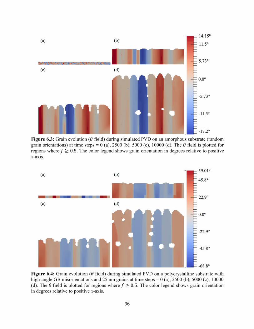
96
Figure 6.3: Grain evolution (𝜃 field) during simulated PVD on an amorphous substrate (random
grain orientations) at time steps = 0 (a), 2500 (b), 5000 (c), 10000 (d). The 𝜃 field is plotted for
regions where 𝑓 ≥ 0.5. The color legend shows grain orientation in degrees relative to positive
x-axis.
Figure 6.4: Grain evolution (𝜃 field) during simulated PVD on a polycrystalline substrate with
high-angle GB misorientations and 25 nm grains at time steps = 0 (a), 2500 (b), 5000 (c), 10000
(d). The 𝜃 field is plotted for regions where 𝑓 ≥ 0.5. The color legend shows grain orientation
in degrees relative to positive x-axis.
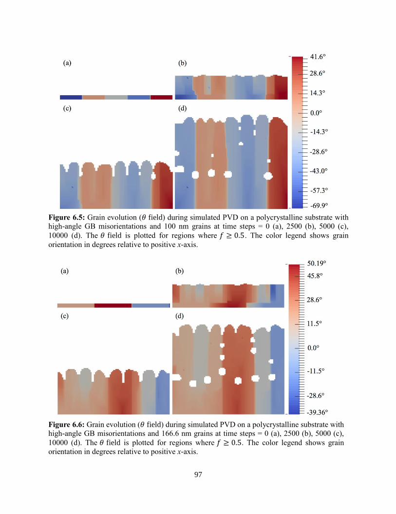
97
Figure 6.5: Grain evolution (𝜃 field) during simulated PVD on a polycrystalline substrate with
high-angle GB misorientations and 100 nm grains at time steps = 0 (a), 2500 (b), 5000 (c),
10000 (d). The 𝜃 field is plotted for regions where 𝑓 ≥ 0.5. The color legend shows grain
orientation in degrees relative to positive x-axis.
Figure 6.6: Grain evolution (𝜃 field) during simulated PVD on a polycrystalline substrate with
high-angle GB misorientations and 166.6 nm grains at time steps = 0 (a), 2500 (b), 5000 (c),
10000 (d). The 𝜃 field is plotted for regions where 𝑓 ≥ 0.5. The color legend shows grain
orientation in degrees relative to positive x-axis.
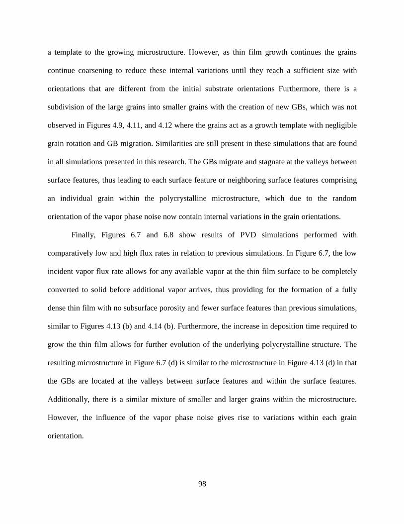
98
a template to the growing microstructure. However, as thin film growth continues the grains
continue coarsening to reduce these internal variations until they reach a sufficient size with
orientations that are different from the initial substrate orientations Furthermore, there is a
subdivision of the large grains into smaller grains with the creation of new GBs, which was not
observed in Figures 4.9, 4.11, and 4.12 where the grains act as a growth template with negligible
grain rotation and GB migration. Similarities are still present in these simulations that are found
in all simulations presented in this research. The GBs migrate and stagnate at the valleys between
surface features, thus leading to each surface feature or neighboring surface features comprising
an individual grain within the polycrystalline microstructure, which due to the random
orientation of the vapor phase noise now contain internal variations in the grain orientations.
Finally, Figures 6.7 and 6.8 show results of PVD simulations performed with
comparatively low and high flux rates in relation to previous simulations. In Figure 6.7, the low
incident vapor flux rate allows for any available vapor at the thin film surface to be completely
converted to solid before additional vapor arrives, thus providing for the formation of a fully
dense thin film with no subsurface porosity and fewer surface features than previous simulations,
similar to Figures 4.13 (b) and 4.14 (b). Furthermore, the increase in deposition time required to
grow the thin film allows for further evolution of the underlying polycrystalline structure. The
resulting microstructure in Figure 6.7 (d) is similar to the microstructure in Figure 4.13 (d) in that
the GBs are located at the valleys between surface features and within the surface features.
Additionally, there is a similar mixture of smaller and larger grains within the microstructure.
However, the influence of the vapor phase noise gives rise to variations within each grain
orientation.

99
Figure 6.7: Phase (top) and grain (bottom) evolution during simulated low flux-rate PVD with
high-angle GB misorientations and 50 nm grains at time steps = 1000 (a) & (c), and 34000 (b)
& (d). The top color legend indicates local density while the bottom legend shows grain
orientation in degrees relative to the positive x-axis.
Figure 6.8: Phase (top) and grain (bottom) evolution during simulated high flux-rate PVD with
high-angle GB misorientations and 50 nm grains at time steps = 1000 (a) & (c), and 5500 (b) &
(d). The top color legend indicates local solid density while the bottom legend shows grain
orientation in degrees relative to the positive x-axis.
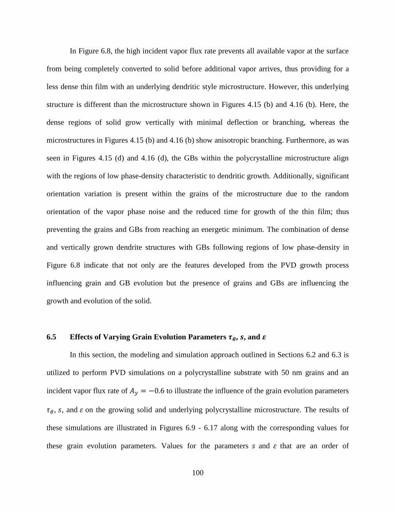
100
In Figure 6.8, the high incident vapor flux rate prevents all available vapor at the surface
from being completely converted to solid before additional vapor arrives, thus providing for a
less dense thin film with an underlying dendritic style microstructure. However, this underlying
structure is different than the microstructure shown in Figures 4.15 (b) and 4.16 (b). Here, the
dense regions of solid grow vertically with minimal deflection or branching, whereas the
microstructures in Figures 4.15 (b) and 4.16 (b) show anisotropic branching. Furthermore, as was
seen in Figures 4.15 (d) and 4.16 (d), the GBs within the polycrystalline microstructure align
with the regions of low phase-density characteristic to dendritic growth. Additionally, significant
orientation variation is present within the grains of the microstructure due to the random
orientation of the vapor phase noise and the reduced time for growth of the thin film; thus
preventing the grains and GBs from reaching an energetic minimum. The combination of dense
and vertically grown dendrite structures with GBs following regions of low phase-density in
Figure 6.8 indicate that not only are the features developed from the PVD growth process
influencing grain and GB evolution but the presence of grains and GBs are influencing the
growth and evolution of the solid.
6.5 Effects of Varying Grain Evolution Parameters 𝝉𝜽, 𝒔, and 𝜺
In this section, the modeling and simulation approach outlined in Sections 6.2 and 6.3 is
utilized to perform PVD simulations on a polycrystalline substrate with 50 nm grains and an
incident vapor flux rate of 𝐴𝑦 = −0.6 to illustrate the influence of the grain evolution parameters
𝜏𝜃, 𝑠, and 휀 on the growing solid and underlying polycrystalline microstructure. The results of
these simulations are illustrated in Figures 6.9 - 6.17 along with the corresponding values for
these grain evolution parameters. Values for the parameters 𝑠 and 휀 that are an order of

101
magnitude smaller or larger than the values presented in this section were found to cause the
numerical solution to become unstable.
First, Figure 6.9 shows PVD simulation results where 𝜏𝜃 = 100 , 𝑠 = 0.01 , and 휀 =
0.005. Here, the grains coarsen through grain rotation and GB migration as expected but in a
non-uniform manner to create larger grains within the polycrystalline microstructure. The grains
contain variations in their orientation in addition to the grains and GBs being more diffuse during
evolution. Based on this simulation, these variations and non-uniformity in growth are due to the
influence of the random noise in the vapor phase combined with the small grain kinetic
coefficient, 𝜏𝜃 , which reduces the amount of grain evolution allowed during the simulation
compared to Section 6.4. However, even in the presence of these variations and
Figure 6.9: Grain evolution (𝜃 field) during simulated PVD on a polycrystalline substrate with
high-angle GB misorientations, 50 nm grains, 𝜏𝜃 = 100, 𝑠 = 0.01, and 휀 = 0.005 at time steps
= 0 (a), 2500 (b), 5000 (c), 10000 (d). The 𝜃 field is plotted for regions where 𝑓 ≥ 0.5. The
color legend shows grain orientation in degrees relative to positive x-axis.
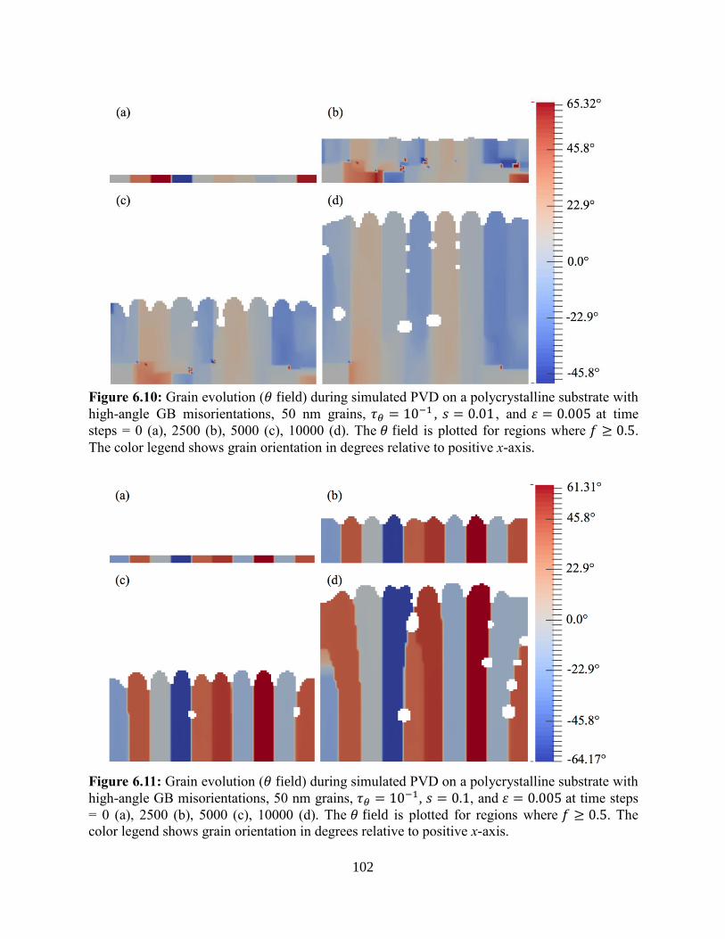
102
Figure 6.10: Grain evolution (𝜃 field) during simulated PVD on a polycrystalline substrate with
high-angle GB misorientations, 50 nm grains, 𝜏𝜃 = 10−1 , 𝑠 = 0.01 , and 휀 = 0.005 at time
steps = 0 (a), 2500 (b), 5000 (c), 10000 (d). The 𝜃 field is plotted for regions where 𝑓 ≥ 0.5.
The color legend shows grain orientation in degrees relative to positive x-axis.
Figure 6.11: Grain evolution (𝜃 field) during simulated PVD on a polycrystalline substrate with
high-angle GB misorientations, 50 nm grains, 𝜏𝜃 = 10−1, 𝑠 = 0.1, and 휀 = 0.005 at time steps
= 0 (a), 2500 (b), 5000 (c), 10000 (d). The 𝜃 field is plotted for regions where 𝑓 ≥ 0.5. The
color legend shows grain orientation in degrees relative to positive x-axis.
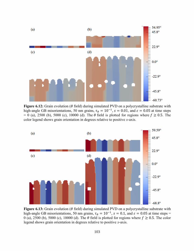
103
Figure 6.12: Grain evolution (𝜃 field) during simulated PVD on a polycrystalline substrate with
high-angle GB misorientations, 50 nm grains, 𝜏𝜃 = 10−1, 𝑠 = 0.01, and 휀 = 0.05 at time steps
= 0 (a), 2500 (b), 5000 (c), 10000 (d). The 𝜃 field is plotted for regions where 𝑓 ≥ 0.5. The
color legend shows grain orientation in degrees relative to positive x-axis.
Figure 6.13: Grain evolution (𝜃 field) during simulated PVD on a polycrystalline substrate with
high-angle GB misorientations, 50 nm grains, 𝜏𝜃 = 10−1, 𝑠 = 0.1, and 휀 = 0.05 at time steps =
0 (a), 2500 (b), 5000 (c), 10000 (d). The 𝜃 field is plotted for regions where 𝑓 ≥ 0.5. The color
legend shows grain orientation in degrees relative to positive x-axis.

104
instabilities, the GBs still align with the valleys between the surface columnar features while the
grains attempt to align with the surface columnar features.
Next, Figures 6.10 and 6.11 shows PVD simulations where 𝜏𝜃 = 10−1, 𝑠 = 0.01, and
휀 = 0.005 and 𝜏𝜃 = 10−1 , 𝑠 = 0.1, and 휀 = 0.005 , respectively. Here, the value of 𝜏𝜃 is an
order of magnitude smaller than in Figure 6.9, thus providing for faster grain evolution kinetics.
With this increase in the rate of grain evolution, Figure 6.10 shows that grains non-uniformly
coarsen as before but with a reduction in the orientation variations and the diffuseness of grains
and GBs. Furthermore, the GBs again align with the valleys between the surface features while
the grains attempt to align with the features. However, in Figures 6.11, where the value of 𝑠 is an
order of magnitude larger, the variations and diffuseness of the grain orientations and GBs within
the polycrystalline microstructure are further reduced during growth and evolution. Additionally,
GBs align with the valleys between the surface features and their growth path is influenced by
the presence of subsurface porosity (cf. Figure 6.11 (d)). As such, the surface features have a
subsurface grain orientation associated with their location in addition to the presence of
subsurface grains whose growth has stagnated and is no longer in contact with the thin film
surface. Therefore, as was shown in these simulations, the strength of the coupling constant 𝑠
controls the diffuseness of these finitely sized grains and GBs, as expected and discussed in
Section 2.3, and when properly determined this parameter reduces or removes the variations and
diffuseness of grain orientations and GBs within the polycrystalline microstructure.
Figures 6.12 and 6.13 illustrate PVD simulation results with 𝜏𝜃 = 10−1, 𝑠 = 0.01, and
휀 = 0.05 and 𝜏𝜃 = 10−1, 𝑠 = 0.1, and 휀 = 0.05, respectively, where the value of 휀 is an order of
magnitude larger than in Figures 6.10 and 6.11. In Figure 6.12, there is initially some variation
and diffuseness in the grains during growth and coarsening that lessens as the film becomes
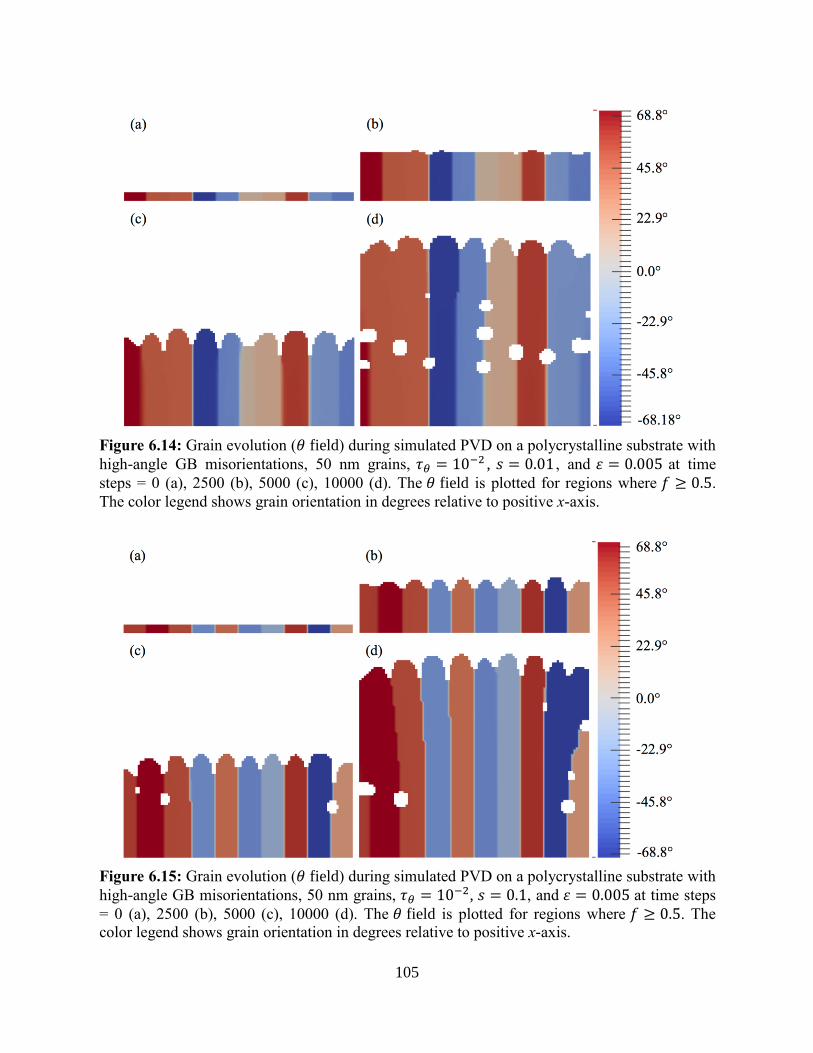
105
Figure 6.14: Grain evolution (𝜃 field) during simulated PVD on a polycrystalline substrate with
high-angle GB misorientations, 50 nm grains, 𝜏𝜃 = 10−2 , 𝑠 = 0.01 , and 휀 = 0.005 at time
steps = 0 (a), 2500 (b), 5000 (c), 10000 (d). The 𝜃 field is plotted for regions where 𝑓 ≥ 0.5.
The color legend shows grain orientation in degrees relative to positive x-axis.
Figure 6.15: Grain evolution (𝜃 field) during simulated PVD on a polycrystalline substrate with
high-angle GB misorientations, 50 nm grains, 𝜏𝜃 = 10−2, 𝑠 = 0.1, and 휀 = 0.005 at time steps
= 0 (a), 2500 (b), 5000 (c), 10000 (d). The 𝜃 field is plotted for regions where 𝑓 ≥ 0.5. The
color legend shows grain orientation in degrees relative to positive x-axis.

106
Figure 6.16: Grain evolution (𝜃 field) during simulated PVD on a polycrystalline substrate with
high-angle GB misorientations, 50 nm grains, 𝜏𝜃 = 10−2, 𝑠 = 0.01, and 휀 = 0.05 at time steps
= 0 (a), 2500 (b), 5000 (c), 10000 (d). The 𝜃 field is plotted for regions where 𝑓 ≥ 0.5. The
color legend shows grain orientation in degrees relative to positive x-axis.
Figure 6.17: Grain evolution (𝜃 field) during simulated PVD on a polycrystalline substrate with
high-angle GB misorientations, 50 nm grains, 𝜏𝜃 = 10−2, 𝑠 = 0.1, and 휀 = 0.05 at time steps =
0 (a), 2500 (b), 5000 (c), 10000 (d). The 𝜃 field is plotted for regions where 𝑓 ≥ 0.5. The color
legend shows grain orientation in degrees relative to positive x-axis.
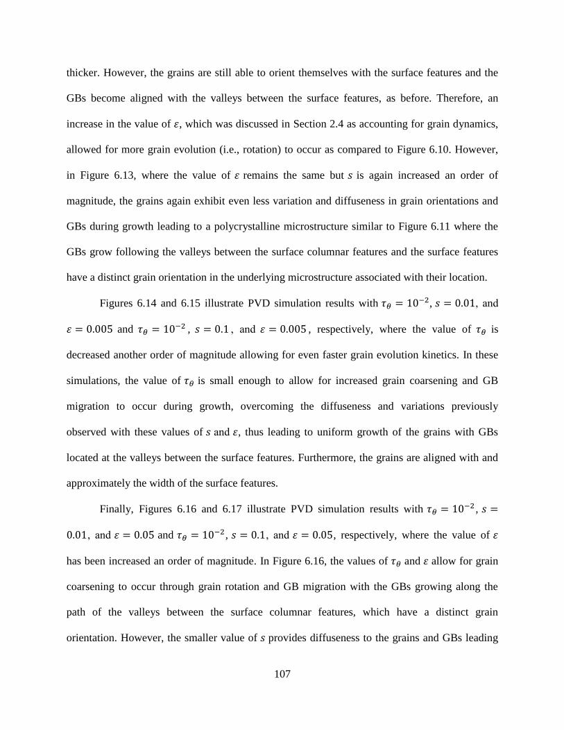
107
thicker. However, the grains are still able to orient themselves with the surface features and the
GBs become aligned with the valleys between the surface features, as before. Therefore, an
increase in the value of 휀, which was discussed in Section 2.4 as accounting for grain dynamics,
allowed for more grain evolution (i.e., rotation) to occur as compared to Figure 6.10. However,
in Figure 6.13, where the value of 휀 remains the same but 𝑠 is again increased an order of
magnitude, the grains again exhibit even less variation and diffuseness in grain orientations and
GBs during growth leading to a polycrystalline microstructure similar to Figure 6.11 where the
GBs grow following the valleys between the surface columnar features and the surface features
have a distinct grain orientation in the underlying microstructure associated with their location.
Figures 6.14 and 6.15 illustrate PVD simulation results with 𝜏𝜃 = 10−2, 𝑠 = 0.01, and
휀 = 0.005 and 𝜏𝜃 = 10−2 , 𝑠 = 0.1 , and 휀 = 0.005 , respectively, where the value of 𝜏𝜃 is
decreased another order of magnitude allowing for even faster grain evolution kinetics. In these
simulations, the value of 𝜏𝜃 is small enough to allow for increased grain coarsening and GB
migration to occur during growth, overcoming the diffuseness and variations previously
observed with these values of 𝑠 and 휀, thus leading to uniform growth of the grains with GBs
located at the valleys between the surface features. Furthermore, the grains are aligned with and
approximately the width of the surface features.
Finally, Figures 6.16 and 6.17 illustrate PVD simulation results with 𝜏𝜃 = 10−2 , 𝑠 =
0.01, and 휀 = 0.05 and 𝜏𝜃 = 10−2, 𝑠 = 0.1, and 휀 = 0.05, respectively, where the value of 휀
has been increased an order of magnitude. In Figure 6.16, the values of 𝜏𝜃 and 휀 allow for grain
coarsening to occur through grain rotation and GB migration with the GBs growing along the
path of the valleys between the surface columnar features, which have a distinct grain
orientation. However, the smaller value of 𝑠 provides diffuseness to the grains and GBs leading
108
to the GBs to becoming thicker. However, in Figure 6.17 where the value of 𝑠 is increased an
order of magnitude (i.e., stronger coupling), this diffuse behavior is removed as the stronger
coupling provide for increased stability to the grain sizes and GBs. Therefore, it is critical to
determine values of 𝜏𝜃, 𝑠, and 휀, which in principle are related to physically relevant quantities,
that will allow for an appropriate rate of grain growth kinetics in addition to grain stability (i.e.,
not unrealistically diffuse) and grain dynamics to be captured by the model when considering a
non-dimensional simulation.
6.6 Summary and Concluding Remarks
In this chapter, a novel free energy functional is developed that combines appropriate
energetics and dynamics to allow for simultaneous simulation of PVD and grain evolution in
single-phase polycrystalline materials within the phase-field modeling framework. This free
energy is used to determine equations of motion, which are then utilized to illustrate the
capability of this novel model in capturing simultaneous thin film solid growth with grain and
GB evolution during PVD conditions. Specifically, this novel phase-field model is used to
investigate the influence of low-angle and high-angle GB misorientation influences in a
polycrystalline substrate, grain size influences in a polycrystalline substrate, and incident vapor
flux rate influences on microstructure evolution, which are then compared to the corresponding
simulation results from utilizing the unidirectional coupling method in Chapter 4. Furthermore,
the grain evolution parameters 𝜏𝜃, 𝑠, and 휀 are varied to illustrate their influence on the evolution
of grains and GBs and the rate evolution within the polycrystalline microstructure during PVD.
The phase-field modeling approach developed in this chapter is an improvement on the
method used in Chapter 4 as it (i) removes the sequential coupling condition between distinct

109
phase-field models and (ii) allows not only for structural features predicted by modeling PVD to
influence the evolution of the underlying microstructure, but the underlying polycrystalline
microstructure features (e.g., grains and GBs) are able to influence the formation and evolution
of structural features predicted by the PVD components. However, this model still contains some
of the limitations that were present in the model described in Chapter 4. First, the formation of
additional stable or metastable phases and preferred growth directions or growth anisotropies is
neglected in this initial model formulation for simplicity. Second, the equations of motion are
developed using dimensionless model parameters that are not linked to physically relevant
quantities, which prevents the calculation of characteristic length and time scales relating to
microstructure features and deposition rates.
Even with the above simplifications and limitations, qualitative observations can be made
regarding the connection and interaction between the thin film structural features and the
underlying polycrystalline features (i.e., grains and GBs), which are found to resemble the
simulation observations and experimental justifications discussed in Chapter 4. First, significant
variations were observed between the resulting polycrystalline microstructure with the low-angle
and high-angle GB misorientation substrates that was due to the large random orientations within
the vapor phase compared to the small orientations within the substrate. However, it was still
observed that grains coarsen through grain rotation and GB migration with the grains attempting
to become aligned with the surface features and the GBs becoming immobilized at the valleys
between the surface columnar features. Next, it was observed that, regardless of initial grain size,
the grains coarsen until they become sufficiently large and growth stagnates with the surface
columnar features being associated with a distinct grain orientation and the GBs located at the
valleys between columnar features. However, using the novel model proposed in this chapter, it

110
was observed that when the initial grains are large enough, a subdivision of the grains occurs;
thus creating several new GBs and smaller grains, which was not fully observed in the sequential
modeling approach of Chapter 4. At a low flux rate (𝐴𝑦 = −0.16), a fully dense thin film
containing some surface roughness and no subsurface features is formed. The increase in
deposition time allows for further grain evolution resulting in a mixture of grain sizes with
orientation variations within each grain in addition to the grains coarsening so that GBs migrate
to the valleys between the surface features. At a high flux rate (𝐴𝑦 = −2.5), a less dense
dendritic style microstructure is formed. However, the dendrite structures exhibit only vertical
growth with no side branching in addition to the GBs following the low phase-density regions;
thus, providing evidence that the presence of grains and GBs now influences the development of
the thin film features during growth. Finally, it was shown that variations in the grain evolution
parameters 𝜏𝜃, 𝑠, and 휀 influence the diffuseness of the grains and the rate at which the grain
kinetics are allowed to occur. Regardless of these variations, grain evolution features observed in
all simulations were also observed here where grains attempt to become align with the surface
columnar features with GBs located at the valleys between the features; leading to each columnar
features being associated with a distinct subsurface grain orientation.

111
Chapter 7: Conclusions and Recommendations
7.1 Summary of Major Scientific Contributions
This dissertation focuses on the development, implementation, and utilization of phase-
field models to investigate phase and microstructure formation, distribution, and evolution in thin
films as a function of initial physical vapor deposition (PVD) processing conditions, e.g. flux
rate, substrate grain orientation, substrate phase distribution, and temperature distribution. Recall
that four main goals were outlined to support this research objective: (i) to develop a phase-field
model for PVD of a single-phase polycrystalline material by leveraging previous phase-field
modeling efforts on ballistic deposition of single-phase materials and grain evolution in
polycrystalline materials, (ii) to develop a phase-field model for PVD of a multiphase material
by leveraging previous phase-field modeling efforts on ballistic deposition of single-phase
materials, evolution of multiphase materials, and phase nucleation, (iii) to develop a novel free

112
energy functional within the phase-field modeling framework for PVD of a single-phase
polycrystalline material, and (iv) to implement these phase-field models into custom numerical
algorithms to illustrate and utilize their capabilities in capturing solid thin film growth via PVD,
grain and grain boundary (GB) evolution, phase evolution and nucleation, and temperature
distribution influences. Combined, these tasks contribute to the advancement of predictive
multiscale modeling of microstructure evolution processes. It is evident that each of these goals
are addressed by the research contained within this dissertation, with the major contributions and
findings summarized as follows:
A method to couple phase-field models of PVD and single-phase polycrystalline
materials was developed. This method was used to simulate PVD of a generic single-
phase polycrystalline metal to investigate the influence of (i) substrates with low-angle
and high-angle GB misorientations, (ii) an amorphous substrate and substrates with
varying grain sizes that are smaller and larger than the thin film surface features that
form, and (iii) varying incident vapor flux rates in thin film feature formation and
subsurface grain evolution. Results show that there are no significant differences in the
evolution of grains and GBs or the resulting microstructures between the low-angle and
high-angle misorientation substrates. Furthermore, as was observed in all simulations,
grains evolve through grain rotation and GB migration until the grains reach sufficient
size where grain coarsening ceases and GBs are aligned with the valleys between surface
columnar features. When the substrate grains are smaller than the surface features, the
grains will coarsen and align with the surface features whereas substrate grains that are
larger than the surface features tend to act as a template for the growing microstructure
with minimal grain rotation or GB migration. However, depending on the potential used
113
to describe the solid phase, a subdivision of grains can occur. Finally, with a
comparatively low incident vapor flux rate, a fully dense thin film with no subsurface
porosity and few pronounced surface features is formed with additional time provided for
the subsurface grain to evolve leading to a mixture of small and large grains. With a
comparatively high flux rate, a less dense thin film with more surface features that are
less pronounced is formed with a subsurface microstructure resembling dendrites. Here,
the increased flux rate reduces the amount of time available for the grains to evolve to an
energetic minimum.
A method to couple phase-field models of PVD and multiphase materials with isotropic
growth kinetics was developed. This method was used to simulate PVD of a generic
metal with two stable solid phases and phase nucleation to (i) investigate the influence of
high temperature (i.e., above the phase transition temperature) PVD on amorphous and
polycrystalline substrates with comparatively low and high interface mobilities, (ii)
investigate the influence of low temperature (i.e., below the phase transition temperature)
PVD of a high temperature phase on a single crystal substrate, (iii) investigate the
influence of a Gaussian temperature distribution with amorphous and polycrystalline
substrates, and (iv) illustrate the ease at which the multiphase PVD model can be
extended to three dimensions and the corresponding surface morphologies and
microstructures that form with varying incident vapor flux rates. Results show that
substrate phase distribution tends to act as a template to the growing microstructure until
the thin film becomes sufficiently thick for the bulk thermodynamics to control phase
growth evolution, which was shown to be influenced by the interface mobility. As the
thin film grows, latent heat is released into the system near the surface causing a

114
temperature gradient to form where the regions near the thin film surface are the hotter
than regions near the substrate, which in turn influences and changes the rate of phase
nucleation throughout the thin film. Finally, imposing a temperature distribution within
the substrate provides regions within the thin film that are above or below the transition
temperature so that multiple phases are stable and coexist.
An algorithm was developed and implemented into the custom numerical codes produced
in this research for multiphase evolution allowing removal of unphysical phase fractions
within the multiphase phase field model using the traditional infinite energy barrier
method for the unphysical phase fractions. This method was shown not only to be easy to
numerically implement but scales all phase fractions in a physically consistent manner
such that the scaling does not produce spurious phases or depend on the labeling or
ordering of the phase fractions.
A novel free energy functional was developed with the appropriate energetics for
allowing simultaneous simulation of PVD and subsurface grain evolution in single-phase
polycrystalline materials. This novel phase-field model was utilized to investigate the
influence of (i) substrates with low-angle and high-angle GB misorientations, (ii) an
amorphous substrate and substrates varying grain sizes that are smaller and larger than
the thin film surface features that form, (iii) varying incident vapor flux rates in thin film
feature formation and subsurface grain evolution, which were compared to the previous
sequential coupling method, and (iv) the grain evolution parameters 𝜏𝜃, 𝑠, and 휀 on the
growing thin film and evolutionary dynamics of the polycrystalline microstructure.
Results show that grains coarsened through grain rotation and GB migration but with
orientation variations due to the random orientation of the vapor phase and the relative

115
size difference in these orientations with the substrate orientations. It was still observed
that grains coarsen until they reach sufficient size and growth stagnates with the surface
columnar features being associated with a distinct grain and GBs being aligned with the
valleys between the surface features. Furthermore, when grains were larger than the
surface features that formed, a subdivision of the grains occurred, thus creating new
smaller grains and GBs. At a comparatively low flux rate, a fully dense thin film with few
pronounced surface features and no subsurface porosity is formed with the increased
deposition time allowing further grain evolution leading to a mixture of grain sizes. At a
comparatively high flux rate, a less dense microstructure was formed where the dendrites
exhibited only vertical growth with the GBs following the regions of low phase-density;
thus indicating that the presence of grains and GBs influences the formation and
evolution of thin film features during growth. Finally, it was shown that variations in the
grain evolution parameters 𝜏𝜃, 𝑠, and 휀 influence the diffuseness of grains, GBs, and the
rate at which grain evolution occurs.
Finally, to address the simulation requirements of these models, custom numerical codes
were developed during the course of this research, employing the finite difference and
conjugate gradient numerical methods outlined in Chapter 3 in order to solve the
equations of motion and perform the simulations presented in this dissertation.
7.2 Recommendations for Future Work
The phase-field simulations in this research provide valid initial observations, which are
compared to experimental observations, based on a first attempt to develop predictive models for
microstructure formation and evolution of polycrystalline and polymorphic materials during
116
PVD. However, several aspects were ignored for simplicity in developing these initial models,
which potentially have significant influences in microstructure evolution processes and require
the development of more complex models. Possible further extensions to refine the predictive
capabilities of these models are outlined as follows:
The free energy functional in Equation 6.1 and equations of motion in Equations 6.2 - 6.4
were proposed as dimensionless quantities; thus preventing the polycrystalline and thin
film features and their rate of evolution from being related to characteristic physical time
and length scales. As such, deriving physical relationships between the model parameters
and physical quantities will allow for quantitative simulations of grain evolution during
various PVD initial conditions and the determination of physically relevant deposition
rates.
The free energy functional in Equation 6.1 is constructed assuming isotropic kinetics, i.e.
the energies of the phase boundaries and GBs are the same at all boundaries. However, it
is known that there are preferred growth directions and anisotropic in real materials.
Therefore, extending this free energy functional to include anisotropic growth of a grain
with a given crystal symmetry will enhance the quantitative nature of the model. These
growth anisotropies are traditionally incorporated through the gradient energy
coefficients in the free energy functional and are a function of the field variables.
The free energy functional in Equation 6.1 has an implied temperature below some
critical temperature to allow for solid growth. Furthermore, grain evolution in real
materials is temperature dependent, as it can increase or decrease the rate of grain
coarsening. As such, developing interfacial gradient quantities or coefficients that are
117
temperature dependent will influence solid growth and grain evolution kinetics and
further extend the capabilities model.
Finally, the free energy functional in Equation 6.1 is constructed to model only a single-
phase material. However, real materials have multiple phases that are present or that can
nucleate under certain conditions. Therefore, extending this free energy to consider the
interactions of additional stable and metastable phases, e.g. phase boundaries and GBs
between phases will provide a major component to developing a physically relevant
phase-field model for simulating microstructure formation and evolution of real materials
under PVD conditions.
118
References
[1] Karabacak, T. (2011) Thin-film growth dynamics with shadowing and re-emission
effects. Journal of Nanophotonics, 5, 1 - 18.
[2] Mahan, J.E. (2000) Physical Vapor Deposition of Thin Films. New York: John Wiley &
Sons.
[3] Mattox, D.M. (2010) Handbook of Physical Vapor Deposition (PVD) Processing.
Oxford: Elsevier.
[4] Ohring, M. (2002) Materials Science of Thin Films. San Diego, CA: Academic Press.
[5] Plummer, J.D., Deal, M. and Griffin, P.D. (2000) Silicon VLSI Technology:
Fundamentals, Practice, and Modeling. Upper Saddle River, NJ. Prentice Hall.
[6] Thornton, J.A. (1977) High Rate Thick Film Growth. Annual Review of Materials
Science, 7, 239 - 260.
[7] Petrov, I., Barna, P.B., Hultman, L. and Greene, J.E. (2003) Microstructural evolution
during thin film growth. Journal of Vacuum Science and Technology A, 21, S117 - S128.
[8] Pusztai, T., Bortel, G. and Granasy, L. (2005) Phase field modeling of polycrystalline
freezing. Materials Science and Engineering A, 413 - 414, 412 - 417.
[9] Bunshah, R.F. and Juntz, R.S. (1973) Influence of Condensation Temperature on
Microstructure and Tensile Properties of Titanium Sheet Produced by High-Rate Physical
Vapor Deposition Process. Metallurgical Transactions, 4, 21 - 26.
[10] Wang, X. (2015) Modeling and understanding materials microstructure evolution driven
by interface energy. Computational Materials Science, 107, 1 - 7.
[11] Krzanowski, J.E. (2004) Phase formation and phase separation in multiphase thin film
hard coatings. Surface & Coatings Technology, 188 - 189, 376 - 383.
[12] Braic, M., Braic, V., Vladescu, A., Zoita, C.N. and Balaceanu, M. (2014) Solid solution
or amorphous phase formation in TiZr-based ternary to quinternary multi-principle-
element films. Progress in Natural Science: Materials International, 24, 305 - 312.
[13] Dragoo, A.L. and Diamond, J.J. (1967) Transitions in Vapor-Deposited Alumina from
300° to 1200°. Journal of the American Ceramic Society, 50, 568 - 574.

119
[14] Kabla, M., Seiner, H., M. Musilova, M., Landa, M. and Shilo, D. (2014) The
relationships between sputter deposition conditions, grain size, and phase transformation
temperatures in NiTi thin films. Acta Materialia, 70, 79 - 91.
[15] Ruppi, S. (2005) Deposition, microstructure and properties of texture-controlled CVD a-
Al2O3 coatings. International Journal of Refractory Metals & Hard Materials, 23, 306 -
316.
[16] Keblinski, P., Maritan, A., Toigo, F., Messier, R. and Banavar, R. (1996) Continuum
model for the growth of interfaces. Physical Review E, 53, 759 - 778.
[17] Simmons, J.P., Wen, Y., Shen, C. and Wang, Y.Z. (2004) Microstructural development
involving nucleation and growth phenomena simulated with the Phase Field method.
Materials Science and Engineering A, 365, 136 - 143.
[18] Yang, Y.G., Johnson, R.A. and Wadley, H.N.G. (1997) A Monte Carlo Simulation of the
Physical Vapor Deposition of Nickel. Acta Materialia, 45, 1455 - 1468.
[19] Boettinger, W.J., Warren, J.A., Beckermann, C. and Karma, A. (2002) Phase-Field
Simulation of Solidification. Annual Review of Materials Research, 32, 163 - 194.
[20] Chen, L.Q. (2002) Phase-Field Models for Microstructure Evolution. Annual Review of
Materials Research, 32, 113 - 140.
[21] Moelans, N., Blanpain, B. and Wollants, P. (2007) An introduction to phase-field
modeling of microstructure evolution. Computer Coupling of Phase Diagrams and
Thermochemistry, 32, 268 - 294.
[22] Thornton, K., Agren, J. and Voorhees, P.W. (2003) Modeling the evolution of phase
boundaries in solids at the meso- and nano-scales. Acta Materialia, 51, 5675 - 5710.
[23] Warren, J.A., Kobayashi, R., Lobkovsky, A.E. and Carter, W.C. (2003) Extending phase
field models of solidification to polycrystalline materials. Acta Materialia, 51, 6035 -
6058
[24] Steinbach, I., Pezzolla, F., Nestler, B., Seeβelberg, M., Prieler, R., Schmitz, G.J. and
Rezende, J.L.L. (1996) A phase field concept for multiphase systems. Physica D, 94, 135
- 147.
[25] Simmons, J.P., Shen, C. and Wang, Y. (2000) Phase Field Modeling of Simultaneous
Nucleation and Growth by Explicitly Incorporating Nucleation Events. Scripta
Materialia, 43, 935 - 942.
[26] Simmons, J.P., Wen, Y., Shen, C. and Wang, Y.Z. (2004) Microstructural development
involving nucleation and growth phenomena simulated with the Phase Field method.
Materials Science and Engineering A, 365, 136 - 143.
120
[27] Provatas, N. and Elder, K. (2010) Phase-Field Methods in Materials Science and
Engineering. John Wiley & Sons.
[28] Xu, H., Matkar, R. and Kyu, T. (2005) Phase-field modeling on morphological landscape
of isotactic polystyrene single crystals. Physical Review E, 72, 011804 (9).
[29] Clouet, E. (2009) Modeling of Nucleation Processes. D. Furrer and S.L. Semiatin (Eds.),
ASM Handbook Volume 22A: Fundamentals of Modeling for Metals Processing (pp. 203
- 219). ASM International.
[30] Oxtoby, D.W. (1998) Nucleation of First-Order Phase Transitions. Accounts of Chemical
Research, 31, 91 - 97.
[31] Heo, T.W. and Chen, L.Q. (2014) Phase-Field Modeling of Nucleation in Solid-State
Phase Transformations. JOM, 66, 1520 - 1528.
[32] Cogswell, D.A. and Carter, W.C. (2011) Thermodynamic phase-field model for
microstructure with multiple components and phases: The possibility of metastable
phases. Physical Review E, 83, 061602.
[33] Toth, G.I., Pusztai, T. and Granasy, L. (2015) Equilibrium and dynamics in multiphase-
field theories: A comparative study and a consistent formulation. arXiv:1508.04311
[cond-mat.mtrl-sci].
[34] Chapra, S.C. and Canale, R.P. (2002) Numerical Methods for Engineers With Software
and Programming Applications. Boston: McGraw-Hill.
[35] Ferziger, J.H. (1998) Numerical Methods for Engineering Applications. New York: John
Wiley & Sons.
[36] Shewchuk, J.R. (1994) An Introduction to the Conjugate Gradient Method Without the
Agonizing Pain. Carnegie Mellon University.
[37] He, W., Bhole, S.D. and Chen, D. (2008) Modeling the dependence of strength on grain
sizes in nanocrystalline materials. Science and Technology of Advanced Materials, 9,
015003.
[38] Cantwell, P.R., Tang, M., Dillon, S.J., Luo, J., Rohrer, G.S. and Harmer, M.P. (2014)
Grain boundary complexions. Acta Materialia, 62, 1 - 48.
[39] Herzig, C. and Divinski, S.V. (2003) Grain Boundary Diffusion in Metals: Recent
Developments. Materials Transactions, 44, 14 - 27.
[40] Steyskal, E.M., Oberdorfer, B., Sprengel, W., Zehetbauer, M., Pippan, R. and Wurschum,
R. (2012) Direct Experimental Determination of Grain Boundary Excess Volume in
Metals. Physical Review Letters, 108, 055504.

121
[41] Islamgaliev, R.K., Pekala, K., Pekala, M. and Valiev, R.Z. (197) The Determination of
the Grain Boundary Widths of Ultrafine Grained Copper and Nickel from Electrical
Resistivity Measurements. Physica Status Solidi (A), 162, 559 - 566.
[42] Prokoshkina, D., Esin, V.A., Wilde, G. and Divinski, S.V. (2013) Grain boundary width,
energy and self-diffusion in nickel: Effect of material purity. Acta Materialia, 61, 5188 -
5197.
[43] Spearot, D.E., Capolungo, L., Qu, J. and Cherkaoui, M. (2008) On the elastic tensile
deformation of <100> bicrystal interfaces in copper. Computational Materials Science,
42, 57 - 67.
[44] Koch, C.C., Youssef, K.M., Scattergood, R.O. and Murty, K.L. (2005) Breakthroughs in
Optimization of Mechanical Properties of Nanostructured Metals and Alloys. Advanced
Engineering Materials, 7, 787 - 794.
[45] McFadden, S.X., Mishra, R.S., Valiev, R.Z., Zhilyaev, A.P. and Mukherjee, A.K. (1999)
Low-temperature superplasticity in nanostructured nickel and metal alloys. Nature, 398,
684 - 686.
[46] Edalati, K. and Horita, Z. (2011) High-pressure torsion of pure metals: Influence of
atomic bond parameters and stacking fault energy on grain size and correlation with
hardness. Acta Materialia, 59, 6831 - 6836.
[47] Jung, Y., Sasaki, T., Tomimatsu, T., Matsunaga, K., Yamamoto, T., Kagawa, Y. and
Ikuhara, Y. (2003) Distribution and structures of nanopores in YSZ-TBC deposited by
EB-PVD. Science and Technology of Advanced Materials, 4, 571 - 574.
[48] Rashkova, B. (2003) Microstructural Characterization of Yttria-Stabilized Zirconia
Thermal Barrier Coating Grown on Sapphire Substrates (Doctoral Dissertation).
University of Stuttgart, Germany.
[49] Wada, K., Yamaguchi, N. and Matsubara, H. (2004) Crystallographic texture evolution
on ZrO2-Y2O3 layers produced by electron beam physical vapor deposition. Surface and
Coatings Technology, 184, 55 - 62.
[50] Gandin, C., Rappaz, M., West, D. and Adams, B.L. (1995) Grain Texture Evolution
during the Columnar Growth of Dendritic Alloys. Thin Solid Films, 26A, 1543 - 1551.
[51] Barna, P.B. and Adamik, M. (1998) Fundamental structure forming phenomena of
polycrystalline films and the structure zone models. Thin Solid Films, 317, 27 - 33.
[52] Melo, L.L., Vaz, A.R., Salvadori, M.C. and Cattani, M. (2004) Grain Sizes and Surface
Roughness in Platinum and Gold Thin Films. Journal of Metastable and Nanocrystalline
Materials, 20 - 21, 623 - 628.
122
[53] Yi, J.N., Li, X.P., Ding, J. and Seet, H.L. (2007) Study of the grain size, particle size, and
roughness of substrate in relation to the magnetic properties of electroplated permalloy.
Journal of Alloys and Compounds, 428, 230 - 236.
[54] Solati, E. and Dorranian, D. (2013) Investigation of the Structure and Properties of
Nanoscale Grain-Size β-Tantalum Thin Films. Molecular Crystals and Liquid Crystals,
571, 67 - 76.
[55] Outemzabet, R., Bouras, N. and Kesri, N. (2007) Microstructure and physical properties
of nanofaceted antimony doped tin oxide thin films deposited by chemical vapor
deposition on different substrates. Thin Solid Films, 515, 6518 - 6520.
[56] Grovenor, C.R.M., Hentzell, H.T.G. and Smith, D.A. (1984) The Development of Grain
Structure During Growth of Metallic Films. Acta Metallurgica, 32, 773 -781.
[57] Wang, C.C., Wang, H., Zheng, X. and Zhu, J. (2005) Role of columnar grain size in
magnetization of La0.8MnO3 thin films grown by pulsed laser deposition. Applied Physics
A, 81, 1423 - 1426.
[58] Yang, Y.G., Johnson, R.A. and Wadley, H.N.G. (1997) A Monte Carlo Simulation of the
Physical Vapor Deposition of Nickel. Acta Materialia, 45, 1455 - 1468.
[59] Wolfe, D.E. and Singh, J. (1999) Microstructural evolution of titanium nitride (TiN)
coatings produced by reactive ion beam-assisted, electron beam physical vapor
deposition (RIDA, ED-PVD). Journal of Materials Science, 34, 29997 - 30006.
[60] Lide, D.R. (2002) CRC Handbook of Chemistry and Physics (83rd ed.). Boca Raton: CRC
Press.
[61] Robie R.A., Hemingway, B.S. and Fisher, J.R. (1984) Thermodynamic Properties of
Minerals and Related Substances at 298.15 K and 1 Bar (105 Pascals) Pressure and at
Higher Temperatures. U.S. Geological Survey Bulletin 1452. Washington: United States
Government Printing Office.
[62] Olmstead, D.L., Holm, E.A. and Foiles, S.M. (2009) Survey of computed grain boundary
properties in face-centered cubic metals - II: Grain boundary mobility. Acta Materialia,
57, 3704 - 3717.
[63] Wang, S. (2006) Molecular dynamics simulation study of grain boundary migration in
nanocrystalline Pd (Doctoral Dissertation). Louisiana State University.
[64] Attard, G. and Barnes, C. (1998) Surfaces. Oxford: Oxford University Press.

123
Appendix A: Description of Research for Popular Publication
124
Designing Advanced Materials with Virtual Physical Vapor Deposition
Tools to Expand Fundamental Understanding, Predict Materials Properties, and Reduce Costs
By: James Stewart
The ability to design specific engineering components, the materials that comprise these
components, and the associated materials processing methods using computational methods is a
major scientific and engineering effort to simulate the influences of entire production processes
before production begins. The focus of these modeling and simulation efforts is to understand
how the processing of materials influences the formation and evolution of a materials
microstructure, which in turn dictates the material’s chemical, mechanical, and electrical
properties that determine possible applications of the material. By predicting the formation and
evolution of a materials microstructure (e.g., grains, grain boundaries, phase formation and
distribution, etc.), and therefore its corresponding properties, the design and development of
advanced materials with specific properties for specific applications can be accelerated with
reduced cost and risk.
James Stewart at the University of Arkansas Institute for Nanoscience & Engineering has
been performing research on developing and employing novel phase-field based models to
describe and simulate physical vapor deposition of polycrystalline and polymorphic materials
under various initial conditions. “These models are utilized to simulate the formation and
evolution of a thin film’s microstructure, e.g. grains, grain boundaries, phase nucleation and
evolution, temperature evolution, etc. during physical vapor deposition and to study how these
microstructure features influence or are influenced by the formation of surface features”, says
Stewart.

125
According to Stewart, “In polycrystalline materials, our research shows that grains and
grain boundaries prefer to be aligned and located in specific patterns in relation to the size and
location of surface features that form during the simulated physical vapor deposition.” Stewart
continues, “Furthermore, in multiphase materials, it was found that the initial temperature
distribution, substrate phase distribution, and interface mobility between material phases can
significantly influence the nucleation of additional stable or metastable phases and the evolution
of any phases that may be present during thin film growth, which can result the formation of
various microstructures.”
Not only can this research act as a guide to academic and industry applications to reduce
exploratory and verification costs to design advanced materials with specific properties, but the
model also allows researchers to test and study new theories on the evolutionary dynamics of
microstructure features that can be compared to existing experiments and extended to include
additional parameters or complex processes to provide the model with greater accuracy. The
Figure 1: Simulated physical vapor deposition for (i) a single-phase polycrystalline material
with an amorphous substrate (a) - (d) illustrating grain coarsening and alignment of grains and
grain boundaries, and (ii) a two-phase material with isotropic growth kinetics, an amorphous
substrate and a Gaussian temperature distribution (e) - (h).
126
methods and findings provided by this novel model provide insight into the connection between
thin film morphology and microstructure evolution processes at the nano to microscale during
physical vapor deposition.

127
Appendix B: Executive Summary of Newly Created Intellectual Property

128
The following list of new intellectual property items were created during the course of
this research and should be considered from both a patent and commercialization perspective.
[1] A mathematical method to couple separate phase-field models for physical vapor
deposition and polycrystalline materials in a sequential algorithm to simulate thin film
growth and grain evolution.
[2] A mathematical method to couple separate phase-field models for physical vapor
deposition and multiphase materials in a sequential algorithm to simulate thin film
growth and phase evolution, phase nucleation, and temperature evolution.
[3] A mathematical / numerical algorithm to enforce the phase fraction interpretation of the
multiphase phase-field model, which removes unphysical phase fractions in a physically
consistent manner and does not depend on the ordering or labeling of the phases.
[4] A free energy functional that contains physically appropriate energetics for modeling and
simulating simultaneous physical vapor deposition and grain evolution of a single-phase
polycrystalline material within the phase-field modeling framework.
[5] Fortran codes to simulate: (i) physical vapor deposition of a single-phase polycrystalline
material using the coupling method in Section 3.2, (ii) physical vapor deposition of a
multiphase material using the coupling method in Section 3.3 in two spatial dimensions,
(iii) physical vapor deposition of multiphase materials using the coupling method in
Section 3.3 in three spatial dimensions, and (iv) physical vapor deposition of a single-
phase polycrystalline material using the single free energy functional in Chapter 6.

129
Appendix C: Potential Patent and Commercialization Aspects of Listed Intellectual
Property

130
C.1 Patentability of Intellectual Property
The newly created intellectual property items listed in Appendix B were considered from
the perspective of whether or not the items could be patented.
[1] This item cannot be patented as abstract ideas such as mathematical formulas, models,
and algorithms themselves are not patentable.
[2] This item cannot be patented as abstract ideas such as mathematical formulas, models,
and algorithms themselves are not patentable.
[3] This item cannot be patented as abstract ideas such as mathematical formulas, models,
and algorithms themselves are not patentable.
[4] This item cannot be patented as abstract ideas such as mathematical formulas, models,
and algorithms themselves are not patentable.
[5] These items can be patented as the mathematical formulas and models are applied and
implemented into numerical codes that provide physically tangible or concrete results.
C.2 Commercialization Prospects
The newly created intellectual property items listed in Appendix B were considered from
the perspective of whether or not the items should be patented.
[1] This item should not be patented, as the details of the content are not patentable.
[2] This item should not be patented, as the details of the content are not patentable.
[3] This item should not be patented, as the details of the content are not patentable.
[4] This item should not be patented, as the details of the content are not patentable.
[5] These items should not be patented, as others are able to utilize and implement the
abstract mathematical formulas and models, which are not patentable, into codes for use.

131
C.3 Possible Prior Disclosure of Intellectual Property
The following newly created intellectual property items were discussed in a public forum
or have published information that could impact the patentability of the items in Appendix B.
[1] The details of this item were presented at the 2015 MRS Fall Meeting & Exhibit, the
TMS 2016 Annual Meeting & Exhibition, and discussed in private communications with
Dr. Douglas E. Spearot.
[2] The details of this item were presented at the 2015 SES Annual Technical Meeting, and
discussed in private communications with Dr. Douglas E. Spearot.
[3] The details of this item were discussed in private communications with Dr. Douglas E.
Spearot.
[4] The details of this item were presented at the TMS 2016 Annual Meeting & Exhibition,
and discussed in private communications with Dr. Douglas E. Spearot.
[5] The details of these items were discussed in private communications with Dr. Douglas E.
Spearot and the custom codes have not been released for outside use.

132
Appendix D: Broader Impacts of Research

133
D.1 Applicability of Research Methods to Other Problems
The theoretical and computational methods used in this research are utilized across
science and engineering disciplines to develop new models and predict microstructural evolution
processes within materials for a variety of real world problems. Extending free energy
functionals to contain additional energetics (e.g., grain misorientation, electric or magnetic fields,
strain, etc.) that corresponds to physically justified quantities is the basis of the phase-field
model. Furthermore, advances in scientific computing allow computational scientists to simulate
physically relevant and realistic situations.
D.2 Impact of Research Results on U.S. and Global Society
The phase-field modeling research method as applied to simulated PVD of polymorphic
and polycrystalline materials does not pose any direct adverse impact on U.S. and global society
nor do the model predictions observed in this research.
D.3 Impact of Research Results on the Environment
The phase-field modeling research method as applied to simulated PVD of polymorphic
and polycrystalline materials does not pose any direct adverse environmental impact nor do the
model predictions observed in this research.

134
Appendix E: Microsoft Project for MicroEP PhD Degree Plan

135

136
Appendix F: Identification of All Software Used in Research and Dissertation Generation

137
Computer 1:
Model Number: Arkansas High Performance Computing Center (AHPCC)
Location: University of Arkansas
Owner: University of Arkansas
Software 1:
Name: Intel Fortran Compiler
Purchased by: University of Arkansas
Computer 2:
Model Number: Dell Precision T3610
Serial Number: BXXBN22
Location: NANO 213B
Owner: University of Arkansas (Dr. Douglas E. Spearot)
Software 1:
Name: Microsoft Office
Purchased by: University of Arkansas Site License
Software 2:
Name: MATLAB
Purchased by: University of Arkansas Site License
Software 3:
Name: ParaView
Purchased by: Open Source
Software 4:
Name: Microsoft Project
Purchased by: University of Arkansas Site License (MicroEP Graduate Program)

138
Appendix G: All Publications Published, Submitted, and Planned

The following research topics from this dissertation are planned for submission during
the Summer and/or Fall of 2016.
[1] From Chapters 4 and 6: A comparison between the sequential and single free energy
functional models for low-angle and high-angle grain boundary substrates. Thus
illustrating the first order features captured by both methods and the higher order features
that are not captured by the sequential approach and requires the use of a single free
energy functional.
[2] From Chapters 4 and 6: A comparison between the sequential and single free energy
functional models for substrates with varying grain sizes and incident vapor flux rates.
Thus illustrating the first order features captured by both methods and the higher order
features that are not captured by the sequential approach and requires the use of a single
free energy functional.
[3] From Chapter 5: The sequential multiphase PVD model with phase nucleation illustrating
the first order growth and evolution features captured by this method.