phase diagram of grain boundary facet and line junctions
TRANSCRIPT
PHYSICAL REVIEW MATERIALS 4, 083604 (2020)
Phase diagram of grain boundary facet and line junctions in silicon
Masud Alam, Liverios Lymperakis ,* and Jörg NeugebauerDepartment of Computational Material Design, Max-Planck-Institut für Eisenforschung GmbH,
Max-Planck Str. 1, 40237 Düsseldorf, Germany
(Received 19 June 2020; accepted 5 August 2020; published 24 August 2020)
The presence of facets and line junctions connecting facets on grain boundaries (GBs) has a strong impact onthe properties of structural, functional, and optoelectronic materials: They govern the mobility of interfaces, thesegregation of impurities, as well the electronic properties. In the present paper, we employ density-functionaltheory and modified embedded atom method calculations to systematically investigate the energetics andthermodynamic stability of these defects. As a prototype system, we consider �3 tilt GBs in Si. By analyzingthe energetics of different faceted GBs, we derive a diagram that describes and predicts the reconstruction ofthese extended defects as a function of facet length and boundary inclination angle. The phase diagram shedslight upon the fundamental mechanisms causing GB faceting phenomena. It demonstrates that the properties offaceting are not determined solely by anisotropic GB energies but by a complex interplay between geometry andmicrostructure, boundary energies as well as long-range strain interactions.
DOI: 10.1103/PhysRevMaterials.4.083604
I. INTRODUCTION
Crystal defects such as grain boundaries (GBs) severelyimpact materials properties [1]. For structural materials, theHall-Petch strengthening of metals [2,3] and the brittle frac-ture induced by preferential segregation of impurities at GBs[4] are characteristic examples of how GBs affect mechanicalproperties. The role of GBs is also substantial in multi- andpolycrystalline optoelectronic materials. Today, multicrys-talline Si (mc-Si) dominates the Si-based photovoltaics indus-try thanks to its lower production cost than single-crystal Si.However, mc-Si has a density of 104 cm−1 GBs [5] and thesedefects as well as their interaction with impurities constituteone major limiting factor in the efficiency of the aforemen-tioned devices. A prominent example is the recombination ofelectrons at GBs. This mechanism constitutes the major elec-trical losses channel in high-performance mc-Si solar cells [6].Indeed, GBs often act as strong gettering centers for metalimpurities due to the presence of over- or undercoordinatedatoms and the different-than-bulk strain. These impurities, theover- or undercoordinated and/or highly strained host atomsmay introduce deep states into the fundamental band gap.Such states would act as recombination centers and reducethe efficiency of solar cells [7].
The �3 tilt GBs with 〈110〉 rotation axis in Si constitutea system of GBs with special fundamental and technolog-ical interest: �3 GBs constitute up to 80% of GBs in Si
Published by the American Physical Society under the terms of theCreative Commons Attribution 4.0 International license. Furtherdistribution of this work must maintain attribution to the author(s)and the published article’s title, journal citation, and DOI. Openaccess publication funded by the Max Planck Society.
ingots grown by dendritic casting [8]. These boundaries arecommonly observed to facet toward the low index {111}and {112} boundaries. The {111} and {112} boundariesare also formed by the dissociation of higher � value GBs[9]. The �3{111} twin boundaries are coherent and can beviewed as hexagonal inclusions into the cubic lattice. Theseboundaries have negligible boundary energy, i.e., less than0.5 meV/Å2 and are electrically inactive. Hence they arepreferred over other electrically active boundaries. On theother hand, the �3 {112} GBs have two stable/metastablestates, the symmetric (S-�3) and the asymmetric (A-�3),with the latter having lower energy. The two states of the�3 {112} GB have different electronic properties. They alsoshow potential as impurity gettering centers: The presence ofa fivefold coordinated atom and highly strained bonds at theS-�3 boundary introduces deep states into the fundamentalband gap while the reconstructed A-�3 GB has no deep statesin the gap [10]. Furthermore, density-functional theory (DFT)calculations show the S-�3 GB to favor interstitial Fe [11]as well as P and As substitutional [10] segregation. Both{112} boundaries also show very different site selectivity forC substitutionals [12].
A striking difference between the A-�3 and S-�3 GBs isthat the latter is commensurate to the underlying coincidencesite lattice (CSL) while the former requires removal of atomsfrom the interface area as well as a rigid shift of the onegrain with respect to the other. Recently, a unique anisotropicsegregation mechanism going beyond the classical planarMcLean-type segregation has been demonstrated at facetedSi GBs [13]. Specifically, by combining DFT with modifiedembedded atom method (MEAM) potential calculations, itwas shown that differences in the local atomic geometry at the�3 {111} and A-�3{112} line junctions associated with thestrain arising from the above-mentioned partial dislocationsare the origin of the aforementioned preferential impurity
2475-9953/2020/4(8)/083604(10) 083604-1 Published by the American Physical Society
ALAM, LYMPERAKIS, AND NEUGEBAUER PHYSICAL REVIEW MATERIALS 4, 083604 (2020){111} {112}
b
Fl
θ
L {}
111 L{112}
L
Fl
bΣ3
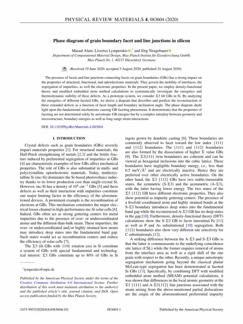
FIG. 1. Schematic representation of a �3 tilt GB (dashed blueline) inclined by θ with respect to {111} faceted toward {111} and{112} facets. L{111} and L{112} are the lengths of the {111} and {112}facets in the {110} plane, respectively, and L is the facet period. F l
denotes the forces acting on the separation line between two facets.These line forces arise from the discontinuity of the interfacial stressat the line junctions. b is the Burgers vector of the dislocation andarises since interfacial translation vectors of {111} and {112} facetsare different.
segregation. However, the driving force that causes facetingin these system is still an open issue.
Following Herring’s thermodynamic arguments, facetingof interfaces is primarily driven by a high anisotropy in theboundary energies and results from the minimization of theinterfacial free energy [14]. The facet length depends not onlyon the energy of the facets but on the interaction energy be-tween dislocations and line forces as well [15,16] (see Fig. 1).Faceting may also be caused by impurities and/or changes incomposition [17–19]: It has been proposed and demonstratedthat faceting and segregation in alloys are strongly interrelatedand are the result of two coupled energy-reduction mecha-nisms.
As has already been mentioned, the �3{111} and both theA-�3 and S-�3 GBs have very different energies (i.e., 0.4vs 55 and 69 meV/Å2, respectively). This is consistent withexperimental evidence that flat �3 tilt boundaries with the〈110〉 rotation axis facet toward {111} and {112} boundaries[13]. However, it is not clear whether this faceting behaviorof Si GBs is an intrinsic property of the GBs, i.e., drivenonly by the anisotropy in the boundary energy with respect tothe inclination angle or mediated by impurities/solute atoms.The presence of stable/metastable reconstructions of the �3{112} GBs increases the complexity of this system: For smallinclination angles with respect to the {111} plane, the bound-ary area of the low-energy {111} facets will be considerablylarger than the area of the {112} facets. At these angles, theinteraction between the partial dislocations inherent to thejunctions with A-�3 facets may dominate and constitute theS-�3 energetically preferential facets. The latter implies thattransitions between facet junction reconstructions may occur,depending on the inclination angle and the facet period. Thiswould drastically influence the electronic properties and theimpurity segregation, as well as the GB mobility of faceted �3GBs. Therefore, a phase diagram of this boundary system thatwould describe the facet junction reconstruction as a functionof the inclination angle and the facet period is critical tounderstand and control the properties of these boundaries.
To address under what conditions faceting occurs, we in-vestigate the energetics, atomic structure, and strain distribu-tion of flat and faceted �3 tilt GBs in Si with the 〈110〉 rotation
axis by employing DFT and large-scale MEAM potentialcalculations. In a first step, we have therefore parameterizeda MEAM Si potential. For this, we use a material propertiesdatabase derived from our as well as previously reportedDFT calculations as well as reported experimental data. Ourcalculations reveal that faceting of tilt �3 GBs is an intrinsicproperty of Si and can occur even in the absence of impuritysegregation. However, line junction and facet reconstructionsare found to sensitively depend on the inclination angle andthe facet length.
The paper is organized as follows. In Sec. II, the method-ology is presented. Section III presents the results on theenergetics, the atomic structure, and the strain associatedwith faceted �3 tilt GBs with 〈110〉 rotation axis. Based onthese calculations, a phase diagram is derived that describesand predicts the facet and line junction reconstructions as afunction of facet period and inclination angles. This phasediagram is shown to provide implications on GB facetingand mobility, impurity segregation, and electronic properties.Finally, Sec. IV summarizes the results. Appendix describesthe parametrization of the MEAM potential.
II. METHODOLOGY
All first-principles calculations were performed by em-ploying DFT and the projector augmented-wave method[20,21]. Both local density approximation (LDA) and gen-eralized gradient approximation (GGA) were employed. Akinetic energy cutoff of 450 eV was used for the expansionof the plane-wave basis set. An equivalent of a 6 × 6 × 6Monkhorst-Pack k-point mesh for the bulk unit cell was usedto sample the Brillouin zone. Atomic positions were relaxeduntil the absolute value of the maximum force on all atomswas less than 0.01 eV/Å.
The generalized stacking fault energies (GSFE) were cal-culated using a diamond crystal with the three primitivevectors oriented along 〈110〉, 〈111〉, and 〈112〉. LDA wasused for exchange and correlation. Supercells consisted often unit cells along the surface normal and a 1 × 1 interfacecell. All DFT calculations of the {111}, S-, and A-{112}�3 GBs were performed using supercells consisting of twomutually compensated GBs and with a 2 × 2 interface cell.The separation distance between the two interfaces was largerthan 30 Å. This separation was validated to be large enough todecouple the two boundaries and to attain boundary energieswith an accuracy better than 0.1 meV/Å2.
All interatomic potential calculations were performed us-ing the molecular dynamics simulator LAMMPS [22]. Theatomic geometries and energies of flat and faceted GBswere obtained by simulated annealing within the isothermal-isobaric ensemble ( NPT). The temperature of the system wasfirst raised to 700 K. It was then cooled to 0.1 K with acooling time of 750 ns. We have explicitly checked that anorder of magnitude slower cooling rate had no effect on boththe energetics and the atomic geometries. The final structuresand energies were then obtained by performing a conjugategradient relaxation of the annealed structures. The conjugategradient minimization was terminated either when the energychange was below 10−6 eV or when all atomic forces werebelow 10−6 eV/Å.
083604-2

PHASE DIAGRAM OF GRAIN BOUNDARY FACET AND … PHYSICAL REVIEW MATERIALS 4, 083604 (2020)
E
DC
A
B
αβ
γ
(a) (b)
<111>
<112>
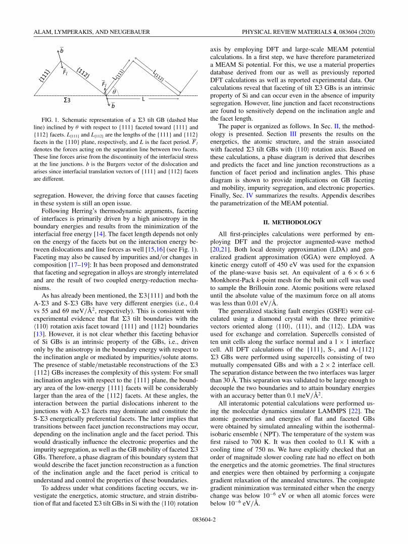
FIG. 2. Relaxed atomic geometry of (a) the S-{112} and (b) theA-{112} GB viewed along 〈110〉. In (a), A and B indicate the five-and seven-atom rings, respectively. α and β are the atoms whichhave to be removed and with a downward shift of the right grainby 1.743 Å form the A-{112} GB. γ denotes the fivefold coordinateatom. In (b), C, D, and E indicate the five-, six-, and seven-atomrings, respectively.
III. RESULTS AND DISCUSSION
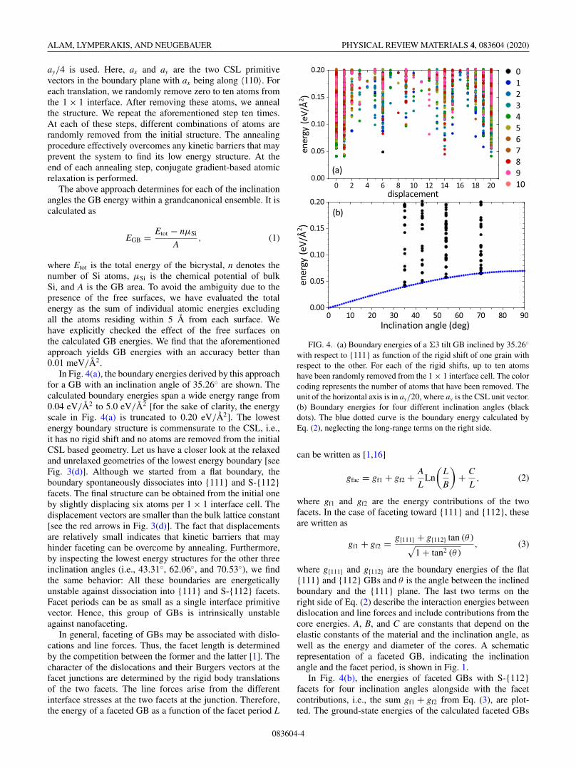
In general, five macroscopic degrees of freedom are nec-essary to define and identify a GB. Three of them define themisorientation of the two neighboring grains. The other twodefine the boundary plane orientation. In addition, to achievea complete macroscopic and microscopic description of theGBs, one has to also consider translations of one grain withrespect to the other, the density, and the exact position ofthe atoms at the GB. An illustrative example that the afore-mentioned five macroscopic parameters alone are inadequateto provide a full description of the lowest energy structuresof GBs is the �3 {112} GB in Si. The atomic geometry ofthis GB as derived by the CSL is shown in Fig. 3(c) and therelaxed structure in Fig. 2(a). It consists of five- and seven-atom-rings which are symmetrically aligned with respect tothe (112) plane. One of the atoms at the boundary planeis overcoordinated, i.e., it has five rather than four bonds.However, high-resolution transmission electron microscopy
investigations observed another interface reconstruction [23].This reconstruction is shown in Fig. 2(b) and consists offive-, six-, and seven-atom rings. Unlike the aforementionedsymmetric geometry, all atoms at the reconstructed 1 × 2boundary plane are fourfold coordinated. It also lacks themirror symmetry. This A-�3 {112} GB in Si indeed has asmaller boundary energy than the symmetric one as shown bypresent and previous DFT calculations [23,24].
In the present paper, we focus on the energetics of �3 tiltGBs having the 〈110〉 rotational axis. This choice fixes fourout of the five macroscopic degrees of freedom. This leavesthe inclination angle of the boundary plane with respect tothe {111} plane as the only free degree of freedom. To de-termine the boundary energy along this parameter, we followtwo different approaches. In the first approach, bicrystals areconstructed using the �3 CSL with the 〈110〉 rotation axis.We consider four different boundary plane inclination angles(35.26◦, 43.31◦, 54.74◦, and 70.53◦) with respect to the {111}plane. The two extreme cases, 0◦ and 90◦, correspond to�3 {111} and S-{112} GBs, respectively. In this approach, theGB planes always coincide with a CSL plane [see Fig. 3(d)].Thus, periodic boundary conditions can be applied in any orall of the three directions [25]. In the second approach, the twograins are terminated by two free surfaces, which are parallelto the GB. Periodic boundary conditions are applied in the GBplane. The thicknesses of the grains normal to the GB rangefrom ≈100 Å to ≈150 Å. This thickness has been found todecouple the free surfaces from the boundary.
Next to the five macroscopic degrees of freedom thatare uniquely defined by the above approach, we need tominimize the GB energy with respect to the microscopicdegrees, i.e., GB translations and atomic densities and posi-tions. This issue is addressed by a heuristic approach: Usingthe above-mentioned bicrystals as input structures, we applyrigid translations on one grain with respect to the other inboth boundary plane directions. A step width of ax/20 and
<111>
<112>
(a) (b) (c) (d)
<111>
<112>
FIG. 3. (a) Lattice points of the two interpenetrating grains denoted by the open and filled circles comprising the �3 CSL of Si. Therectangle indicates the unit cell of the CSL. Large and small circles denote points at the two different (110) planes. (b), (c) Schematicrepresentations of the �3 {111} and �3 S-{112} GBs, respectively. The dashed lines indicate the boundary planes. In (c), the shaded areasdenote the characteristic five- and seven-atom ring pattern of the S-{112} GB. (d) �3 GB inclined by 35.26◦ with respect to {111}. The dashedline denote the planes of the flat unrelaxed GB and the rectangle the orthogonal unit cell of the corresponding CSL. The shaded regions indicatethe {111} and symmetric {112} facets that are formed after relaxation. The red arrows denote the displacements of atoms that result in thefaceted GB.
083604-3
ALAM, LYMPERAKIS, AND NEUGEBAUER PHYSICAL REVIEW MATERIALS 4, 083604 (2020)
ay/4 is used. Here, ax and ay are the two CSL primitivevectors in the boundary plane with ax being along 〈110〉. Foreach translation, we randomly remove zero to ten atoms fromthe 1 × 1 interface. After removing these atoms, we annealthe structure. We repeat the aforementioned step ten times.At each of these steps, different combinations of atoms arerandomly removed from the initial structure. The annealingprocedure effectively overcomes any kinetic barriers that mayprevent the system to find its low energy structure. At theend of each annealing step, conjugate gradient-based atomicrelaxation is performed.
The above approach determines for each of the inclinationangles the GB energy within a grandcanonical ensemble. It iscalculated as
EGB = Etot − nμSi
A, (1)
where Etot is the total energy of the bicrystal, n denotes thenumber of Si atoms, μSi is the chemical potential of bulkSi, and A is the GB area. To avoid the ambiguity due to thepresence of the free surfaces, we have evaluated the totalenergy as the sum of individual atomic energies excludingall the atoms residing within 5 Å from each surface. Wehave explicitly checked the effect of the free surfaces onthe calculated GB energies. We find that the aforementionedapproach yields GB energies with an accuracy better than0.01 meV/Å2.
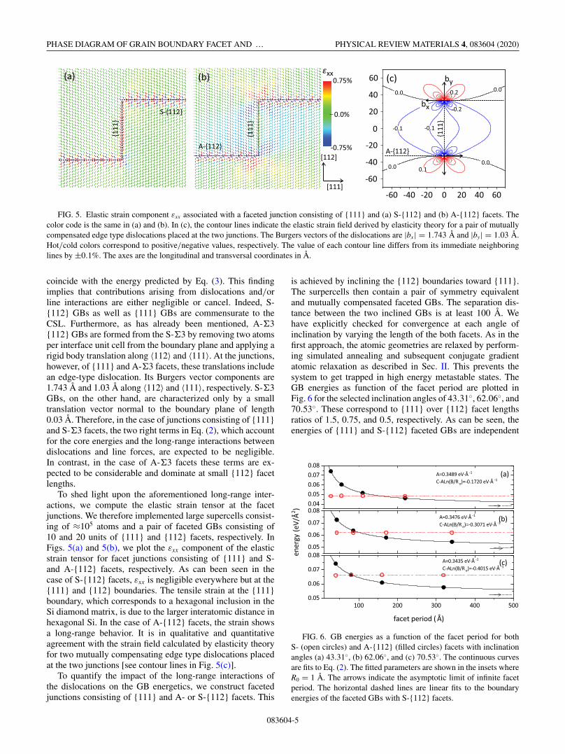
In Fig. 4(a), the boundary energies derived by this approachfor a GB with an inclination angle of 35.26◦ are shown. Thecalculated boundary energies span a wide energy range from0.04 eV/Å2 to 5.0 eV/Å2 [for the sake of clarity, the energyscale in Fig. 4(a) is truncated to 0.20 eV/Å2]. The lowestenergy boundary structure is commensurate to the CSL, i.e.,it has no rigid shift and no atoms are removed from the initialCSL based geometry. Let us have a closer look at the relaxedand unrelaxed geometries of the lowest energy boundary [seeFig. 3(d)]. Although we started from a flat boundary, theboundary spontaneously dissociates into {111} and S-{112}facets. The final structure can be obtained from the initial oneby slightly displacing six atoms per 1 × 1 interface cell. Thedisplacement vectors are smaller than the bulk lattice constant[see the red arrows in Fig. 3(d)]. The fact that displacementsare relatively small indicates that kinetic barriers that mayhinder faceting can be overcome by annealing. Furthermore,by inspecting the lowest energy structures for the other threeinclination angles (i.e., 43.31◦, 62.06◦, and 70.53◦), we findthe same behavior: All these boundaries are energeticallyunstable against dissociation into {111} and S-{112} facets.Facet periods can be as small as a single interface primitivevector. Hence, this group of GBs is intrinsically unstableagainst nanofaceting.
In general, faceting of GBs may be associated with dislo-cations and line forces. Thus, the facet length is determinedby the competition between the former and the latter [1]. Thecharacter of the dislocations and their Burgers vectors at thefacet junctions are determined by the rigid body translationsof the two facets. The line forces arise from the differentinterface stresses at the two facets at the junction. Therefore,the energy of a faceted GB as a function of the facet period L
FIG. 4. (a) Boundary energies of a �3 tilt GB inclined by 35.26◦
with respect to {111} as function of the rigid shift of one grain withrespect to the other. For each of the rigid shifts, up to ten atomshave been randomly removed from the 1 × 1 interface cell. The colorcoding represents the number of atoms that have been removed. Theunit of the horizontal axis is in ay/20, where ay is the CSL unit vector.(b) Boundary energies for four different inclination angles (blackdots). The blue dotted curve is the boundary energy calculated byEq. (2), neglecting the long-range terms on the right side.
can be written as [1,16]
gfac = gf1 + gf2 + A
LLn
(L
B
)+ C
L, (2)
where gf1 and gf2 are the energy contributions of the twofacets. In the case of faceting toward {111} and {112}, theseare written as
gf1 + gf2 = g{111} + g{112} tan (θ )√1 + tan2 (θ )
, (3)
where g{111} and g{112} are the boundary energies of the flat{111} and {112} GBs and θ is the angle between the inclinedboundary and the {111} plane. The last two terms on theright side of Eq. (2) describe the interaction energies betweendislocation and line forces and include contributions from thecore energies. A, B, and C are constants that depend on theelastic constants of the material and the inclination angle, aswell as the energy and diameter of the cores. A schematicrepresentation of a faceted GB, indicating the inclinationangle and the facet period, is shown in Fig. 1.
In Fig. 4(b), the energies of faceted GBs with S-{112}facets for four inclination angles alongside with the facetcontributions, i.e., the sum gf1 + gf2 from Eq. (3), are plot-ted. The ground-state energies of the calculated faceted GBs
083604-4
PHASE DIAGRAM OF GRAIN BOUNDARY FACET AND … PHYSICAL REVIEW MATERIALS 4, 083604 (2020)
{111}
S-{112}
0.75%
-0.75%
0.0%
[112]
[111]
εxx
A-{112}
{111}
(b)(a)0.00.0
0.00.0
A-{112}
{111}
by(c)
0-20-40-60 20 40 60
0
-20
-40
-60
20
40
60
0.1
-0.2
0.2
-0.1 -0.1
bx
FIG. 5. Elastic strain component εxx associated with a faceted junction consisting of {111} and (a) S-{112} and (b) A-{112} facets. Thecolor code is the same in (a) and (b). In (c), the contour lines indicate the elastic strain field derived by elasticity theory for a pair of mutuallycompensated edge type dislocations placed at the two junctions. The Burgers vectors of the dislocations are |bx| = 1.743 Å and |by| = 1.03 Å.Hot/cold colors correspond to positive/negative values, respectively. The value of each contour line differs from its immediate neighboringlines by ±0.1%. The axes are the longitudinal and transversal coordinates in Å.
coincide with the energy predicted by Eq. (3). This findingimplies that contributions arising from dislocations and/orline interactions are either negligible or cancel. Indeed, S-{112} GBs as well as {111} GBs are commensurate to theCSL. Furthermore, as has already been mentioned, A-�3{112} GBs are formed from the S-�3 by removing two atomsper interface unit cell from the boundary plane and applying arigid body translation along 〈112〉 and 〈111〉. At the junctions,however, of {111} and A-�3 facets, these translations includean edge-type dislocation. Its Burgers vector components are1.743 Å and 1.03 Å along 〈112〉 and 〈111〉, respectively. S-�3GBs, on the other hand, are characterized only by a smalltranslation vector normal to the boundary plane of length0.03 Å. Therefore, in the case of junctions consisting of {111}and S-�3 facets, the two right terms in Eq. (2), which accountfor the core energies and the long-range interactions betweendislocations and line forces, are expected to be negligible.In contrast, in the case of A-�3 facets these terms are ex-pected to be considerable and dominate at small {112} facetlengths.
To shed light upon the aforementioned long-range inter-actions, we compute the elastic strain tensor at the facetjunctions. We therefore implemented large supercells consist-ing of ≈105 atoms and a pair of faceted GBs consisting of10 and 20 units of {111} and {112} facets, respectively. InFigs. 5(a) and 5(b), we plot the εxx component of the elasticstrain tensor for facet junctions consisting of {111} and S-and A-{112} facets, respectively. As can been seen in thecase of S-{112} facets, εxx is negligible everywhere but at the{111} and {112} boundaries. The tensile strain at the {111}boundary, which corresponds to a hexagonal inclusion in theSi diamond matrix, is due to the larger interatomic distance inhexagonal Si. In the case of A-{112} facets, the strain showsa long-range behavior. It is in qualitative and quantitativeagreement with the strain field calculated by elasticity theoryfor two mutually compensating edge type dislocations placedat the two junctions [see contour lines in Fig. 5(c)].
To quantify the impact of the long-range interactions ofthe dislocations on the GB energetics, we construct facetedjunctions consisting of {111} and A- or S-{112} facets. This
is achieved by inclining the {112} boundaries toward {111}.The surpercells then contain a pair of symmetry equivalentand mutually compensated faceted GBs. The separation dis-tance between the two inclined GBs is at least 100 Å. Wehave explicitly checked for convergence at each angle ofinclination by varying the length of the both facets. As in thefirst approach, the atomic geometries are relaxed by perform-ing simulated annealing and subsequent conjugate gradientatomic relaxation as described in Sec. II. This prevents thesystem to get trapped in high energy metastable states. TheGB energies as function of the facet period are plotted inFig. 6 for the selected inclination angles of 43.31◦, 62.06◦, and70.53◦. These correspond to {111} over {112} facet lengthsratios of 1.5, 0.75, and 0.5, respectively. As can be seen, theenergies of {111} and S-{112} faceted GBs are independent
FIG. 6. GB energies as a function of the facet period for bothS- (open circles) and A-{112} (filled circles) facets with inclinationangles (a) 43.31◦, (b) 62.06◦, and (c) 70.53◦. The continuous curvesare fits to Eq. (2). The fitted parameters are shown in the insets whereR0 = 1 Å. The arrows indicate the asymptotic limit of infinite facetperiod. The horizontal dashed lines are linear fits to the boundaryenergies of the faceted GBs with S-{112} facets.
083604-5
ALAM, LYMPERAKIS, AND NEUGEBAUER PHYSICAL REVIEW MATERIALS 4, 083604 (2020)
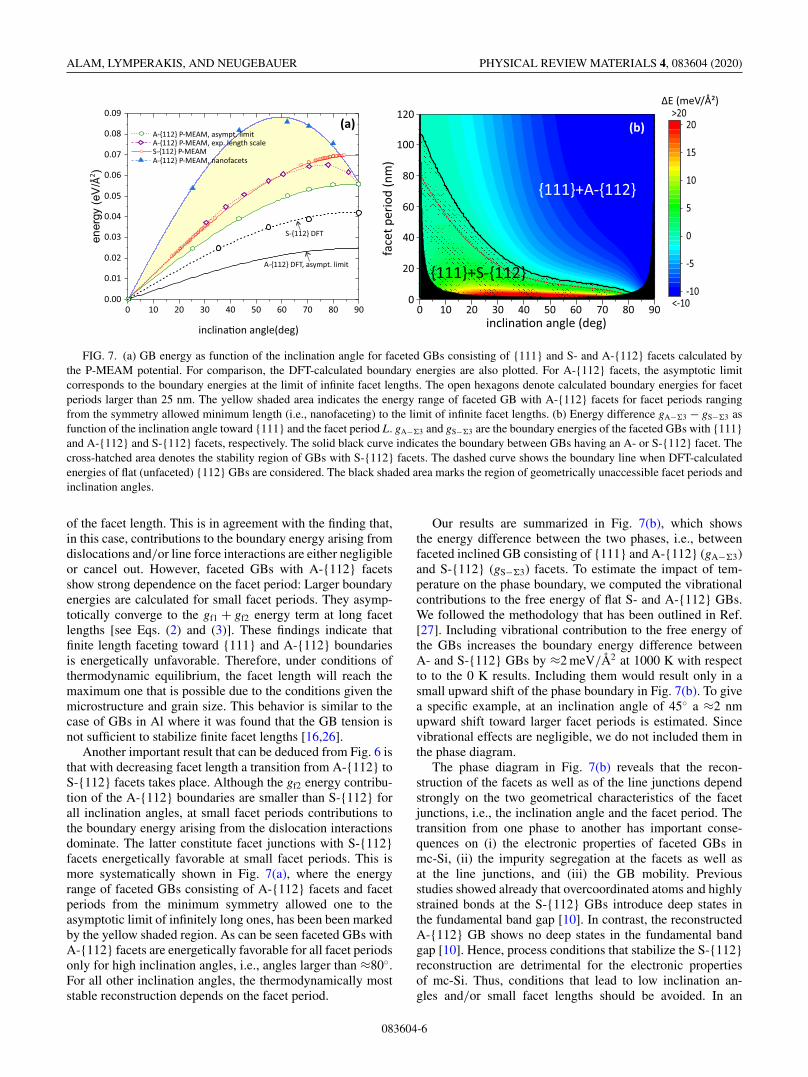
FIG. 7. (a) GB energy as function of the inclination angle for faceted GBs consisting of {111} and S- and A-{112} facets calculated bythe P-MEAM potential. For comparison, the DFT-calculated boundary energies are also plotted. For A-{112} facets, the asymptotic limitcorresponds to the boundary energies at the limit of infinite facet lengths. The open hexagons denote calculated boundary energies for facetperiods larger than 25 nm. The yellow shaded area indicates the energy range of faceted GB with A-{112} facets for facet periods rangingfrom the symmetry allowed minimum length (i.e., nanofaceting) to the limit of infinite facet lengths. (b) Energy difference gA−�3 − gS−�3 asfunction of the inclination angle toward {111} and the facet period L. gA−�3 and gS−�3 are the boundary energies of the faceted GBs with {111}and A-{112} and S-{112} facets, respectively. The solid black curve indicates the boundary between GBs having an A- or S-{112} facet. Thecross-hatched area denotes the stability region of GBs with S-{112} facets. The dashed curve shows the boundary line when DFT-calculatedenergies of flat (unfaceted) {112} GBs are considered. The black shaded area marks the region of geometrically unaccessible facet periods andinclination angles.
of the facet length. This is in agreement with the finding that,in this case, contributions to the boundary energy arising fromdislocations and/or line force interactions are either negligibleor cancel out. However, faceted GBs with A-{112} facetsshow strong dependence on the facet period: Larger boundaryenergies are calculated for small facet periods. They asymp-totically converge to the gf1 + gf2 energy term at long facetlengths [see Eqs. (2) and (3)]. These findings indicate thatfinite length faceting toward {111} and A-{112} boundariesis energetically unfavorable. Therefore, under conditions ofthermodynamic equilibrium, the facet length will reach themaximum one that is possible due to the conditions given themicrostructure and grain size. This behavior is similar to thecase of GBs in Al where it was found that the GB tension isnot sufficient to stabilize finite facet lengths [16,26].
Another important result that can be deduced from Fig. 6 isthat with decreasing facet length a transition from A-{112} toS-{112} facets takes place. Although the gf2 energy contribu-tion of the A-{112} boundaries are smaller than S-{112} forall inclination angles, at small facet periods contributions tothe boundary energy arising from the dislocation interactionsdominate. The latter constitute facet junctions with S-{112}facets energetically favorable at small facet periods. This ismore systematically shown in Fig. 7(a), where the energyrange of faceted GBs consisting of A-{112} facets and facetperiods from the minimum symmetry allowed one to theasymptotic limit of infinitely long ones, has been been markedby the yellow shaded region. As can be seen faceted GBs withA-{112} facets are energetically favorable for all facet periodsonly for high inclination angles, i.e., angles larger than ≈80◦.For all other inclination angles, the thermodynamically moststable reconstruction depends on the facet period.
Our results are summarized in Fig. 7(b), which showsthe energy difference between the two phases, i.e., betweenfaceted inclined GB consisting of {111} and A-{112} (gA−�3)and S-{112} (gS−�3) facets. To estimate the impact of tem-perature on the phase boundary, we computed the vibrationalcontributions to the free energy of flat S- and A-{112} GBs.We followed the methodology that has been outlined in Ref.[27]. Including vibrational contribution to the free energy ofthe GBs increases the boundary energy difference betweenA- and S-{112} GBs by ≈2 meV/Å2 at 1000 K with respectto to the 0 K results. Including them would result only in asmall upward shift of the phase boundary in Fig. 7(b). To givea specific example, at an inclination angle of 45◦ a ≈2 nmupward shift toward larger facet periods is estimated. Sincevibrational effects are negligible, we do not included them inthe phase diagram.
The phase diagram in Fig. 7(b) reveals that the recon-struction of the facets as well as of the line junctions dependstrongly on the two geometrical characteristics of the facetjunctions, i.e., the inclination angle and the facet period. Thetransition from one phase to another has important conse-quences on (i) the electronic properties of faceted GBs inmc-Si, (ii) the impurity segregation at the facets as well asat the line junctions, and (iii) the GB mobility. Previousstudies showed already that overcoordinated atoms and highlystrained bonds at the S-{112} GBs introduce deep states inthe fundamental band gap [10]. In contrast, the reconstructedA-{112} GB shows no deep states in the fundamental bandgap [10]. Hence, process conditions that stabilize the S-{112}reconstruction are detrimental for the electronic propertiesof mc-Si. Thus, conditions that lead to low inclination an-gles and/or small facet lengths should be avoided. In an
083604-6

PHASE DIAGRAM OF GRAIN BOUNDARY FACET AND … PHYSICAL REVIEW MATERIALS 4, 083604 (2020)
experimental or industrial setup, this could be achieved bylong annealing that drives the system toward thermodynamicequilibrium and thus large grains.
The elastic strain of both S- and A-{112} GBs show a peri-odic pattern with alternating compressive and tensile regionsalong 〈111〉 [see Figs. 5(a) and 5(b)]. Explicitly studyingsegregation of impurities to a GB is beyond the scope ofthe present paper. However, the results of impurity-free GBsprovide some qualitative insight into impurity segregation.In this respect, it is important to note that the εxx strainextends deep into the bulk at the S-{112} facets. Thus dif-ferent induced segregation profiles at S- and A-{112} GBsare expected [10,28]. Hence, the segregation profile will bea function of inclination angle and facet period and will bethus qualitatively described by the phase diagram if Fig. 7(b).The strain field at the {111} and S-{112} line junctions isshort range compared to the range of the strain field associatedwith flat S-{112} GBs. On the other hand, the strain fieldat {111} and A-{112} junctions is long range and originatesfrom the presence of edge-type dislocation at these junctions.The latter, in combination with the lack of mirror symmetryof the A facet, results in two different topologies and impuritysegregation potentials at the two line junctions of these GBfacets. Indeed, a recent study showed that the aforementioneddifference in the topology of the facet junction in mc-Si causesasymmetric impurity segregation at {111} and A-{112} facetjunctions [13].
GB disconnections are GB line defects. Generally, theyhave both step and dislocation character and play a crucialrole on the shear coupled migration [29]. Recent TEM inves-tigations on Au bicrystals revealed the lack of lattice defectsat the core of disconnections with a height of two latticespacings at �11(113) coherent GBs [30]. These boundariesshowed a layer by layer migration. It was also reported that theshear-induced migration of these GBs was fully reversible andnot affected by the presence of preexisting lattice or GB dis-locations. This situation is in accord to the twin defects in Siwhere disconnections are {112} steps at the {111} boundary.This corresponds to small facet periods or small inclinationangles. Hence, as it is shown in Fig. 7(b), the steps consistof S-{112} facets, i.e., there are no GB dislocations at theline junctions. Therefore, a similar mechanism as described isexpected to govern the shear induced migration of twins in Si,i.e., migration will be fully reversible and will not be affectedby the presence of other extended lattice defects.
IV. CONCLUSIONS
In the present paper, we have employed DFT and large-scale MEAM potential calculations to study the structure,energetics, and strain associated with �3 tilt GBs havingthe 〈110〉 rotation axis in Si. Based on these calculations,we derive a phase diagram of these boundaries. This phasediagram demonstrates that (i) these GBs are intrinsicallyunstable against faceting toward {111} and {112} facets and(ii) the properties of the facets and of the line junctions isthe result of an intricate interplay between GB energies andlong-range strain interactions. Specifically, we find that atlow misorientation angles and/or small facet periods, long-range interactions dominate and S-{112} facets are favored.
Nevertheless, at large facet periods and inclination angles,the lower energy of the A-{112} facets compensate the straininteractions and these facets are energetically favored.
The significance of being able to construct such defectphase diagrams goes beyond the case of GBs in mc-Si.They shed light upon GB faceting phenomena, specificallyin conjunction with the materials’ microstructure. The pic-ture deduced by this phase diagram contradicts the commonperception that the properties of faceting are merely drivenby the anisotropic GB energies. Although anistropic GB en-ergies are a prerequisite for GB faceting, the phase diagramreveals that higher energy metastable GB phases are stabilizedby thermodynamics and not kinetics when constituting thefacets at line junctions. This insight provides critical infor-mation when designing electronic and structural materials:Microstructures that allow for large facet periods stabilizeline junctions accommodated by dislocations. In contrast,fine granular structures that limit facet periods promote linejunctions without extended line defects and long-range strainfields. This also has immediate implications on the topologyof line junctions, the strain-driven impurities’ segregation, andmobility of GBs. In general, GB phase diagrams that highlightthe interplay between geometry, GB energies, and long-rangestrain fields constitute an indispensable tool in describing,predicting, and designing materials’ microstructure.
ACKNOWLEDGMENT
The authors would like to acknowledge fruitful discussionswith Dr. Christian Liebscher.
APPENDIX: MEAM POTENTIAL PARAMETRIZATION
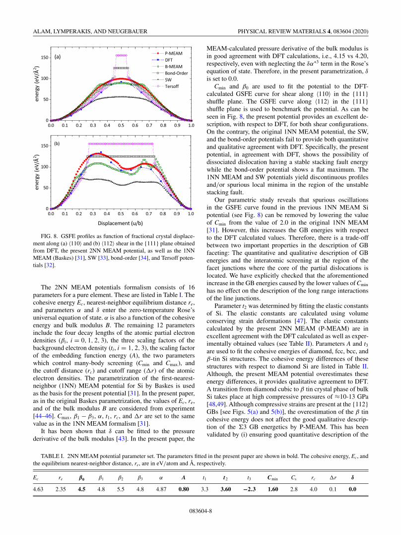
A large number of valence force field models have beendeveloped and applied to study defects in Si—among others,Tersoff [32], Stillinger-Weber (SW) [33], bond-order poten-tials [34,35], and MEAM potentials [36,37]. However, appli-cation of these potentials to study important materials proper-ties such as GSFE reveals critical shortcomings. Specifically,they fail to provide a quantitative and qualitative descriptionof GSFE curves with respect to DFT (see Fig. 8). The GSFEis a material property which relates dislocation cores andthe intrinsic ductility of the material. Smooth GSFE curvescan also be considered as a benchmark of the interatomicscreening under shear conditions.
The second-nearest-neighbor (2NN) MEAM potential is amodification of the original MEAM potential [31] and par-tially include 2NN interactions. 2NN MEAM potentials havebeen parametrized and employed to a wide range of elementsand alloys (see Ref. [38] and NIST Interatomic PotentialsRepository [39–41]). In the present paper, we parametrizeand employ a 2NN MEAM potential to investigate facetingof GBs in Si. A detailed description of the 2NN MEAMformalism can be found in Ref. [42]. Here the parametrizationof the potential is presented. Although the correlation ofthe parameters to physical properties is complicated, someparameters play a more dominant role on certain physicalproperties [43]. This allows us to apply a parametric studyand systematically fit the parameters to these properties.
083604-7
ALAM, LYMPERAKIS, AND NEUGEBAUER PHYSICAL REVIEW MATERIALS 4, 083604 (2020)
FIG. 8. GSFE profiles as function of fractional crystal displace-ment along (a) 〈110〉 and (b) 〈112〉 shear in the {111} plane obtainedfrom DFT, the present 2NN MEAM potential, as well as the 1NNMEAM (Baskes) [31], SW [33], bond-order [34], and Tersoff poten-tials [32].
The 2NN MEAM potentials formalism consists of 16parameters for a pure element. These are listed in Table I. Thecohesive energy Ec, nearest-neighbor equilibrium distance re,and parameters α and δ enter the zero-temperature Rose’suniversal equation of state. α is also a function of the cohesiveenergy and bulk modulus B. The remaining 12 parametersinclude the four decay lengths of the atomic partial electrondensities (βi, i = 0, 1, 2, 3), the three scaling factors of thebackground electron density (ti, i = 1, 2, 3), the scaling factorof the embedding function energy (A), the two parameterswhich control many-body screening (Cmin and Cmax), andthe cutoff distance (rc) and cutoff range (r) of the atomicelectron densities. The parametrization of the first-nearest-neighbor (1NN) MEAM potential for Si by Baskes is usedas the basis for the present potential [31]. In the present paper,as in the original Baskes parametrization, the values of Ec, re,and of the bulk modulus B are considered from experiment[44–46]. Cmax, β1 − β3, α, t1, rc, and r are set to the samevalue as in the 1NN MEAM formalism [31].
It has been shown that δ can be fitted to the pressurederivative of the bulk modulus [43]. In the present paper, the
MEAM-calculated pressure derivative of the bulk modulus isin good agreement with DFT calculations, i.e., 4.15 vs 4.20,respectively, even with neglecting the δα∗3 term in the Rose’sequation of state. Therefore, in the present parametrization, δ
is set to 0.0.Cmin and β0 are used to fit the potential to the DFT-
calculated GSFE curve for shear along 〈110〉 in the {111}shuffle plane. The GSFE curve along 〈112〉 in the {111}shuffle plane is used to benchmark the potential. As can beseen in Fig. 8, the present potential provides an excellent de-scription, with respect to DFT, for both shear configurations.On the contrary, the original 1NN MEAM potential, the SW,and the bond-order potentials fail to provide both quantitativeand qualitative agreement with DFT. Specifically, the presentpotential, in agreement with DFT, shows the possibility ofdissociated dislocation having a stable stacking fault energywhile the bond-order potential shows a flat maximum. The1NN MEAM and SW potentials yield discontinuous profilesand/or spurious local minima in the region of the unstablestacking fault.
Our parametric study reveals that spurious oscillationsin the GSFE curve found in the previous 1NN MEAM Sipotential (see Fig. 8) can be removed by lowering the valueof Cmin from the value of 2.0 in the original 1NN MEAM[31]. However, this increases the GB energies with respectto the DFT calculated values. Therefore, there is a trade-offbetween two important properties in the description of GBfaceting: The quantitative and qualitative description of GBenergies and the interatomic screening at the region of thefacet junctions where the core of the partial dislocations islocated. We have explicitly checked that the aforementionedincrease in the GB energies caused by the lower values of Cmin
has no effect on the description of the long range interactionsof the line junctions.
Parameter t2 was determined by fitting the elastic constantsof Si. The elastic constants are calculated using volumeconserving strain deformations [47]. The elastic constantscalculated by the present 2NN MEAM (P-MEAM) are inexcellent agreement with the DFT calculated as well as exper-imentally obtained values (see Table II). Parameters A and t3are used to fit the cohesive energies of diamond, fcc, bcc, andβ-tin Si structures. The cohesive energy differences of thesestructures with respect to diamond Si are listed in Table II.Although, the present MEAM potential overestimates theseenergy differences, it provides qualitative agreement to DFT.A transition from diamond cubic to β tin crystal phase of bulkSi takes place at high compressive pressures of ≈10-13 GPa[48,49]. Although compressive strains are present at the {112}GBs [see Figs. 5(a) and 5(b)], the overestimation of the β tincohesive energy does not affect the good qualitative descrip-tion of the �3 GB energetics by P-MEAM. This has beenvalidated by (i) ensuring good quantitative description of the
TABLE I. 2NN MEAM potential parameter set. The parameters fitted in the present paper are shown in bold. The cohesive energy, Ec, andthe equilibrium nearest-neighbor distance, re, are in eV/atom and Å, respectively.
Ec re β0 β1 β2 β3 α A t1 t2 t3 Cmin Cs rc r δ
4.63 2.35 4.5 4.8 5.5 4.8 4.87 0.80 3.3 3.60 −2.3 1.60 2.8 4.0 0.1 0.0
083604-8

PHASE DIAGRAM OF GRAIN BOUNDARY FACET AND … PHYSICAL REVIEW MATERIALS 4, 083604 (2020)
TABLE II. Calculated physical properties of Si using the present 2NN MEAM potential (P-MEAM) as well as previous 1NN MEAM(B-MEAM) [31], bond order (E-bond order) [34], and SW [33] potentials compared to DFT and experimental data. All the properties are fordiamond cubic Si unless otherwise denoted. Edia is the cohesive energy of Si in the ground-state diamond crystal and E denotes the cohesiveenergy differences between the diamond and the fcc, bcc, and β-tin Si structures in meV/atom. The lattice parameters a are in Å and thebulk modulus and the elastic constants in GPa. The energies of the 1 × 1 (110), (110), and (111) surfaces are denoted as E(100), E(110), andE(111), respectively, and the GB energies of the {111} and S- and A-{112}, denoted as E�3{111}, ES−�3{112}, and EA−�3{112}, respectively, are inmeV/Å2. The vacancy formation energy Ev is in eV.
P-MEAM B-MEAM E-bond order SW DFT Experimental
diamond Edia –4.63 –4.63 –4.628 –4.336 –4.75f,–4.65d –4.62i
a 5.431 5.427 5.429 5.431 5.403a, 5.43d 5.431e
fcc-dia E 771.21 468.89 652.24 396.28 449a, 537.48b, 566d
a 4.282 4.20 3.85 4.14 3.817a, 3.866b, 3.885d
bcc-dia E 754.85 419.85 505.97 281.04 432a, 519.69b, 525d
a 3.312 3.198 3.044 3.24 3.044a, 3.087b, 3.088d
β tin -dia E 613.75 320.86 423.14 199.68 212a, 295.46d
a 5.079 4.95 4.87 4.97 4.91a, 4.97d
c/a 0.553 0.545 0.527 0.56 0.55a, 0.55d
Bulk modulus B 96.53 96.89 98.38 101.18 96.19a 99h
B′ 4.20 4.22 4.4 2.92 4.15a 4.2h
Elastic constant C11 162.40 162.44 169.33 151.42 160c 166e
C12 65.58 65.44 65.18 76.73 63c 64e
C44 77.74 73.25 60.41 56.44 82c 80e
Ev 3.45 2.94 3.13 4.33 3.64a
E{100} 124.08 102.25 121.86 147. 02 147.93c 132.95f
E{110} 94.17 118.10 76.47 103.96 104.86c 94.25f
E{111} 78.69 102.56 62.35 84.88 107.36c 76.77f
ES−�3{112} 69.89 66.50 59.75 59.38 42.24a, 41.8g
EA−�3{112} 55.3 50.52 51.01 43.16 24.86a, 29.3g
E�3{111} 0.40 0.0 0.0 0.0 0.42a, 0.6g
aand; bdenote DFT-calculated properties employing LDA and GGA, respectively.cReference [50].dReference [51].eReference [52].fReference [53].gReference [11].hReference [54].iReference [44].
GSFE including a large number of highly deformed structuresat the interface and (ii) demonstrating a qualitative descriptionof the energetics and the atomic volumes of the competingbulk crystal phases. These validation benchmarks show thatP-MEAM provides an excellent qualitative description of �3GB energetics and atomic structures.
Using the P-MEAM, we calculate the GB formation ener-gies of �3 {111} and {112} tilt GBs with the 〈110〉 rotationaxis. The GB energies of {111} and S-{112} are 0.4 and69.89 meV/Å2, respectively. The GB energy of the A-{112}is by 14.59 meV/Å2 lower than its symmetric counterpart.
As has already been discussed, the P-MEAM calculated ener-gies of the {112} GBs are overestimated. However, the GBenergy difference between A- and S-{112} is in excellentagreement with the DFT results (17.38 meV/Å2). Moreover,the P-MEAM calculated elastic constants are in excellentagreement to DFT. These agreements imply that the straininteraction between the facet junctions as well as transitionsbetween S- and A-{112} GBs as function of inclination angleand/or facet length are correctly described by P-MEAM [seeFig. 7(b)]. Thus, the present MEAM potential provides anexcellent qualitative description of faceting.
[1] A. P. Sutton and R. W. Balluffi, Interfaces in Crystalline Mate-rials, Monographs on the Physics and Chemistry of Materials,Vol. 51 (Clarendon Press, Oxford, 1996).
[2] E. O. Hall, Proc. Phys. Soc. Sec. B 64, 742 (1951).[3] R. W. Armstrong, Mater. Trans. 55, 2 (2014).[4] M. F. R. Schweinfest and A. Paxton, Nature 432, 1008 (2004).[5] K. Scheerschmidt and M. Werner, Phys. Status Solidi A 202,
2368 (2005).
[6] F. Schindler, A. Fell, R. Müller, J. Benick, A. Richter, F.Feldmann, P. Krenckel, S. Riepe, M. C. Schubert, and S. W.Glunz, Sol. Energy Mater. Sol. Cells 185, 198 (2018).
[7] A. Peaker, V. Markevich, B. Hamilton, G. Parada, A. Dudas,A. Pap, E. Don, B. Lim, J. Schmidt, L. Yu, Y. Yoon, and G.Rozgonyi, Phys. Status Solidi A 209, 1884 (2012).
[8] K. M. Yeh, C. K. Hseih, W. C. Hsu, and C. W. Lan, Prog.Photovolt: Res. Appl. 18, 265 (2010).
083604-9

ALAM, LYMPERAKIS, AND NEUGEBAUER PHYSICAL REVIEW MATERIALS 4, 083604 (2020)
[9] A. Garg, W. A. T. Clark, and J. P. Hirth, Philos. Mag. A 59, 479(1989).
[10] D. Zhao and Y. Li, Acta Mater. 168, 52 (2019).[11] B. Ziebarth, M. Mrovec, C. Elsässer, and P. Gumbsch, Phys.
Rev. B 91, 035309 (2015).[12] D. Zhao and Y. Li, J. Alloys Compd. 712, 599 (2017).[13] C. H. Liebscher, A. Stoffers, M. Alam, L. Lymperakis, O.
Cojocaru-Mirédin, B. Gault, J. Neugebauer, G. Dehm, C.Scheu, and D. Raabe, Phys. Rev. Lett. 121, 015702 (2018).
[14] C. Herring, Phys. Rev. 82, 87 (1951).[15] A. P. Sutton and R. W. Balluffi, Interfaces in Crystalline Mate-
rials, Monographs on the Physics and Chemistry of Materials,Vol. 51 (Clarendon Press, Oxford, 1996), Chap. 4.
[16] J. C. Hamilton, D. J. Siegel, I. Daruka, and F. Léonard, Phys.Rev. Lett. 90, 246102 (2003).
[17] T. Ference and R. Balluffi, Scr. Metall. 22, 1929 (1988).[18] T. Hsieh and R. Balluffi, Acta Metall. 37, 2133 (1989).[19] H. Zhao, L. Huber, W. Lu, N. J. Peter, D. An, F. De Geuser, G.
Dehm, D. Ponge, J. Neugebauer, B. Gault, and D. Raabe, Phys.Rev. Lett. 124, 106102 (2020).
[20] G. Kresse and J. Furthmüller, Phys. Rev. B 54, 11169(1996).
[21] G. Kresse and J. Hafner, Phys. Rev. B 47, 558 (1993).[22] S. Plimpton, J. Comput. Phys. 117, 1 (1995).[23] N. Sakaguchi, H. Ichinose, and S. Watanabe, Mater. Trans. 48,
2585 (2007).[24] C. B. Feng, J. L. Nie, X. T. Zu, M. M. Al-Jassim, and Y. Yan, J.
Appl. Phys. 106, 113506 (2009).[25] L. Lymperakis, M. Friák, and J. Neugebauer, Eur. Phys. J. Spec.
Top. 177, 41 (2009).[26] Z. Wu, Y. Zhang, and D. Srolovitz, Acta Mater. 57, 4278
(2009).[27] A. I. Duff, L. Lymperakis, and J. Neugebauer, Phys. Status
Solidi B 252, 855 (2015).[28] D. Zhao and Y. Li, Comput. Mater. Sci. 143, 80 (2018).[29] J. Han, S. L. Thomas, and D. J. Srolovitz, Prog. Mater. Sci. 98,
386 (2018).[30] Q. Zhu, G. Cao, J. Wang, C. Deng, J. L. abd Ze Zhang, and S. X.
Mao, Nat. Commun. 10, 156 (2019).[31] M. I. Baskes, Phys. Rev. B 46, 2727 (1992).
[32] J. Tersoff, Phys. Rev. B 39, 5566 (1989).[33] F. H. Stillinger and T. A. Weber, Phys. Rev. B 31, 5262 (1985).[34] P. Erhart and K. Albe, Phys. Rev. B 71, 035211 (2005).[35] P. Käshammer and T. Sinno, J. Appl. Phys. 118, 095301 (2015).[36] K. Kang and W. Cai, Philos. Mag. 87, 2169 (2007).[37] T. J. Lenosky, B. Sadigh, E. Alonso, V. V. Bulatov, T. D. de
la Rubia, J. Kim, A. F. Voter, and J. D. Kress, Model. Simul.Mater. Sci. Eng. 8, 825 (2000).
[38] B.-J. Lee, W.-S. Ko, H.-K. Kim, and E.-H. Kim, Calphad 34,510 (2010).
[39] https://www.ctcms.nist.gov/potentials, Website DOI:10.18434/m37.
[40] C. A. Becker, F. Tavazza, Z. T. Trautt, and R. A. B. de Macedo,Curr. Opin. Solid State Mater. Sci. 17, 277 (2013).
[41] L. M. Hale, Z. T. Trautt, and C. A. Becker, Model. Simul. Mater.Sci. Eng. 26, 055003 (2018).
[42] B. Jelinek, S. Groh, M. F. Horstemeyer, J. Houze, S. G. Kim,G. J. Wagner, A. Moitra, and M. I. Baskes, Phys. Rev. B 85,245102 (2012).
[43] B.-J. Lee, M. I. Baskes, H. Kim, and Y. K. Cho, Phys. Rev. B64, 184102 (2001).
[44] B. Farid and R. W. Godby, Phys. Rev. B 43, 14248 (1991).[45] Y. Okada and Y. Tokumaru, J. Appl. Phys. 56, 314 (1984).[46] J. J. Hall, Phys. Rev. 161, 756 (1967).[47] O. Beckstein, J. E. Klepeis, G. L. W. Hart, and O. Pankratov,
Phys. Rev. B 63, 134112 (2001).[48] A. Mujica, A. Rubio, A. Muñoz, and R. J. Needs, Rev. Mod.
Phys. 75, 863 (2003).[49] W. Purwanto, H. Krakauer, and S. Zhang, Phys. Rev. B 80,
214116 (2009).[50] L. Pastewka, A. Klemenz, P. Gumbsch, and M. Moseler, Phys.
Rev. B 87, 205410 (2013).[51] J. F. Justo, M. Z. Bazant, E. Kaxiras, V. V. Bulatov, and S. Yip,
Phys. Rev. B 58, 2539 (1998).[52] W. M. Haynes, CRC Handbook of Chemistry and Physics (CRC
Press, Boca Raton, FL, 2014).[53] R. Jaccodine, J. Electrochem. Soc. 110, 524 (1963).[54] T. Soma and H. M. Kagaya, in Properties of Silicon (The
Institution of Electrical Engineers, Inspec, London, 1988),pp. 33–36.
083604-10