perturbation of au-assisted planar gaas nanowire growth...
TRANSCRIPT
Perturbation of Au-assisted planar GaAs nanowire growth by p-type dopant impurities
Ryan S. Dowdy, Chen Zhang, Parsian K. Mohseni, Seth A. Fortuna, Jian-Guo Wen, James J. Coleman, and Xiuling Li*
Department of Electrical and Computer Engineering, Micro and Nanotechnology Laboratory, and Materials Research Laboratory, University of Illinois, Urbana, IL 61801, USA
Abstract: III-V compound semiconductor nanowires (NWs), with their direct bandgaps and high mobilities, have been shown to be promising materials for many applications including solar cells, light emitting diodes, transistors, and lasers. Self-aligned, twin-plane-defect free, planar GaAs NWs can be grown by metalorganic chemical vapor deposition (MOCVD) through the Au-assisted vapor-liquid-solid mechanism. In this report, <110> planar GaAs NW growth on GaAs (100) substrates is perturbed by introducing common p-type dopant impurities, zinc (Zn) or carbon (C), and characterized structurally and electrically. The implications of the results on planar NW growth and doping mechanism are discussed.
© 2013 Optical Society of America
OCIS codes: (160.4236) Nanomaterials; (130.5990) Semiconductors; (160.4670) Optical materials; (310.3840) Materials and process characterization.
References and links 1. R. S. Wagner and W. C. Ellis, “Vapor-liquid-solid mechanism of single crystal growth,” Appl. Phys. Lett. 4(5),
89–90 (1964). 2. Y. Y. Wu and P. D. Yang, “Direct observation of vapor-liquid-solid nanowire growth,” J. Am. Chem. Soc.
123(13), 3165–3166 (2001). 3. C. P. Svensson, T. Mårtensson, J. Trägårdh, C. Larsson, M. Rask, D. Hessman, L. Samuelson, and J. Ohlsson,
“Monolithic GaAs/InGaP nanowire light emitting diodes on silicon,” Nanotechnology 19(30), 305201 (2008). 4. M. Li, R. B. Bhiladvala, T. J. Morrow, J. A. Sioss, K. K. Lew, J. M. Redwing, C. D. Keating, and T. S. Mayer,
“Bottom-up assembly of large-area nanowire resonator arrays,” Nat. Nanotechnol. 3(2), 88–92 (2008). 5. S. A. Fortuna and X. Li, “GaAs MESFET with a high-mobility self-assembled planar nanowire channel,” IEEE
Electron Device Lett. 30(6), 593–595 (2009). 6. R. Dowdy, D. A. Walko, S. A. Fortuna, and X. Li, “Realization of unidirectional planar GaAs nanowires on
GaAs (110) substrates,” IEEE Electron Device Lett. 33(4), 522–524 (2012). 7. S. A. Fortuna, J. Wen, I. S. Chun, and X. Li, “Planar GaAs nanowires on GaAs (100) substrates: Self-aligned,
nearly twin-defect free, and transfer-printable,” Nano Lett. 8(12), 4421–4427 (2008). 8. M. S. Gudiksen, L. J. Lauhon, J. Wang, D. C. Smith, and C. M. Lieber, “Growth of nanowire superlattice
structures for nanoscale photonics and electronics,” Nature 415(6872), 617–620 (2002). 9. A. Maaßdorf and M. Weyers, “In-situ etching of GaAs/AlxGaAs by CBr4,” J. Cryst. Growth 310(23), 4754–4756
(2008). 10. D. E. Perea, E. R. Hemesath, E. J. Schwalbach, J. L. Lensch-Falk, P. W. Voorhees, and L. J. Lauhon, “Direct
measurement of dopant distribution in an individual vapour-liquid-solid nanowire,” Nat. Nanotechnol. 4(5), 315–319 (2009).
11. D. Stichtenoth, K. Wegener, C. Gutsche, I. Regolin, F. J. Tegude, W. Prost, M. Seibt, and C. Ronning, “p-type doping of GaAs nanowires,” Appl. Phys. Lett. 92(16), 163107 (2008).
12. C. Gutsche, I. Regolin, K. Blekker, A. Lysov, W. Prost, and F. J. Tegude, “Controllable p-type doping of GaAs nanowires during vapor-liquid-solid growth,” J. Appl. Phys. 105(2), 024305 (2009).
13. C. Gutsche, A. Lysov, I. Regolin, K. Blekker, W. Prost, and F.-J. Tegude, “n-type doping of vapor–liquid–solid grown GaAs nanowires,” Nanoscale Res. Lett. 6, 65 (2011).
14. M. T. Borgström, E. Norberg, P. Wickert, H. A. Nilsson, J. Trägårdh, K. A. Dick, G. Statkute, P. Ramvall, K. Deppert, and L. Samuelson, “Precursor evaluation for in situ InP nanowire doping,” Nanotechnology 19(44), 445602 (2008).
15. A. C. Ford, S. Chuang, J. C. Ho, Y. L. Chueh, Z. Fan, and A. Javey, “Patterned p-doping of InAs nanowires by gas-phase surface diffusion of Zn,” Nano Lett. 10(2), 509–513 (2010).
#195494 - $15.00 USD Received 12 Aug 2013; revised 6 Sep 2013; accepted 6 Sep 2013; published 18 Sep 2013(C) 2013 OSA 1 October 2013 | Vol. 3, No. 10 | DOI:10.1364/OME.3.001687 | OPTICAL MATERIALS EXPRESS 1687
16. Z. Ikonic, G. P. Srivastava, and J. C. Inkson, “Optical properties of twinning superlattices in diamond-type and zinc-blende-type semiconductors,” Phys. Rev. B Condens. Matter 52(19), 14078–14085 (1995).
17. Z. Ikonić, G. P. Srivastava, and J. C. Inkson, “Electronic properties of twin boundaries and twinning superlattices in diamond-type and zinc-blende-type semiconductors,” Phys. Rev. B Condens. Matter 48(23), 17181–17193 (1993).
18. R. E. Algra, M. Hocevar, M. A. Verheijen, I. Zardo, G. G. Immink, W. J. van Enckevort, G. Abstreiter, L. P. Kouwenhoven, E. Vlieg, and E. P. Bakkers, “Crystal structure transfer in core/shell nanowires,” Nano Lett. 11(4), 1690–1694 (2011).
19. M. H. M. van Weert, A. Helman, W. van den Einden, R. E. Algra, M. A. Verheijen, M. T. Borgström, G. Immink, J. J. Kelly, L. P. Kouwenhoven, and E. P. A. M. Bakkers, “Zinc incorporation via the Vapor-Liquid-Solid mechanism into InP Nanowires,” J. Am. Chem. Soc. 131(13), 4578–4579 (2009).
20. R. E. Algra, M. A. Verheijen, M. T. Borgström, L. F. Feiner, G. Immink, W. J. van Enckevort, E. Vlieg, and E. P. Bakkers, “Twinning superlattices in indium phosphide nanowires,” Nature 456(7220), 369–372 (2008).
21. R. E. Algra, M. A. Verheijen, L. F. Feiner, G. G. Immink, W. J. Enckevort, E. Vlieg, and E. P. Bakkers, “The role of surface energies and chemical potential during nanowire growth,” Nano Lett. 11(3), 1259–1264 (2011).
22. X. Miao, C. Zhang, and X. Li, “Monolithic barrier-all-around high electron mobility transistor with planar GaAs nanowire channel,” Nano Lett. 13(6), 2548–2552 (2013).
23. R. S. Dowdy, D. A. Walko, and X. Li, “Relationship between planar GaAs nanowire growth direction and substrate orientation,” Nanotechnology 24(3), 035304 (2013).
24. S. M. Sze, Physics of Semiconductor Devices (Wiley-Interscience, 1969). 25. H. Okamoto and T. Massalski, “The Au-C (gold-carbon) system,” J. Phase Equilibria 5, 378–379 (1984). 26. S. Vinaji, A. Lochthofen, W. Mertin, I. Regolin, C. Gutsche, W. Prost, F. J. Tegude, and G. Bacher, “Material
and doping transitions in single GaAs-based nanowires probed by Kelvin probe force microscopy,” Nanotechnology 20(38), 385702 (2009).
27. P. Caroff, K. A. Dick, J. Johansson, M. E. Messing, K. Deppert, and L. Samuelson, “Controlled polytypic and twin-plane superlattices in III-V nanowires,” Nat. Nanotechnol. 4(1), 50–55 (2009).
28. Q. Xiong, J. Wang, and P. C. Eklund, “Coherent twinning phenomena: towards twinning superlattices in III-V semiconducting nanowires,” Nano Lett. 6(12), 2736–2742 (2006).
29. H. J. Joyce, J. Wong-Leung, Q. Gao, H. H. Tan, and C. Jagadish, “Phase perfection in zinc Blende and Wurtzite III-V nanowires using basic growth parameters,” Nano Lett. 10(3), 908–915 (2010).
30. S. A. Fortuna and X. Li, “Metal-catalyzed semiconductor nanowires: a review on the control of growth directions,” Semicond. Sci. Technol. 25(2), 024005 (2010).
1. Introduction
Semiconductor nanowire (NW) research continues to gain momentum due to its unique geometry and associated optical and electronic properties. III-V compound semiconductor NWs, with their direct bandgaps and high mobilities, have been shown to be promising materials for many applications including solar cells, light emitting diodes, lasers, and transistors. The widely used vapor-liquid-solid (VLS) NW growth method [1], using metallic seed particles to facilitate one dimensional anisotropic single crystal growth [2], has specific characteristics that result in interesting phenomena in the grown NWs. The NW diameter is strongly correlated to the seed particle size, which allows for a vast range of scalability that does not rely on lithographic techniques. Researchers are utilizing the unique optical [3], mechanical [4] and electrical [5] properties of VLS semiconductor NWs to create a new generation of devices that are smaller, faster, and cheaper. Conventionally grown VLS wires usually grow preferentially in the <111> crystal directions which generally coincide with out-of-plane directions for common substrates. This leads to incompatibility issues when integrating as-grown NWs with traditional planar processing technologies without removing them from their native substrates. Recently, our research group has developed controlled growth of self-aligned planar <110> and <100> GaAs NW arrays on GaAs (100) and (110) substrates, respectively, using metalorganic chemical vapor deposition (MOCVD) via the Au-assisted VLS mechanism [6, 7]. Planar NWs have the potential to bridge the gap between the benefits of NWs shown in research and practical manufacturability, as well as enable monolithic lateral p-n junction and heterojunction formation [8] for optoelectronic applications.
Impurity doping is essential to any semiconductor devices. Zinc (Zn) and carbon (C) are both important p-type dopants in III-V semiconductors. Zinc is one of the most commonly used p-type dopants for GaAs, readily available in its metalorganic precursors (DEZn or
#195494 - $15.00 USD Received 12 Aug 2013; revised 6 Sep 2013; accepted 6 Sep 2013; published 18 Sep 2013(C) 2013 OSA 1 October 2013 | Vol. 3, No. 10 | DOI:10.1364/OME.3.001687 | OPTICAL MATERIALS EXPRESS 1688
DMZn). It is non-amphoteric, unlike silicon and carbon. It does not have the etch-back issues of carbon tetrachloride or tetrabromide [9]. Several groups have done extensive work on studying and controlling dopants in vertical <111> NWs [10–14], including through Zn implantation [11], zinc diffusion [15] and in situ incorporation of zinc [12]. The dopant incorporation can take place either through the seed by VLS growth mode or onto the sidewall surface by unassisted vapor phase epitaxy (VPE) mode [10, 14]. Although for Ge and many other VLS NWs, it appears that most dopants reside in the thin epitaxial layers that form on the NW sidewall contributed from non-VLS growth [10], it has been confirmed that Zn incorporates through the Au seed in vertical GaAs VLS NWs [12]. However, the understanding of dopant incorporation in NWs via VLS growth and the effect of dopants on NW growth is not yet mature.
In this paper we report on the effect of p-type dopants on the growth of planar GaAs NWs on (100) GaAs substrates. In particular, we investigate the formation of twinning superlattices (TSLs) induced by p-type dopants in planar GaAs NWs, which are otherwise free of twin-plane defects. TSLs in NWs have been projected to introduce minibands [16], direct carrier generation-recombination transitions [17], and increased sidewall phonon scattering [18]. Our work should shed some light on the control of TSL formation in planar NWs including its onset, periodicity, and electrical activity, as well as the growth mechanism of planar VLS NWs.
2. Experimental details
The GaAs NWs were grown by MOCVD, operating at atmospheric pressure using Au colloidal nanoparticles as seeds. Trimethylgallium (TMGa) and arsine (AsH3) were used as Ga and As precursors, respectively. Diethylzinc (DEZn), dimenthyzinc (DMZn) and carbon tetrabromide (CBr4) were used as the p-type dopant impurity precursors. H2 was used as the carrier gas. Au colloids, with sizes ranging from 20 to 250nm, were dispersed on epi-ready semi-insulating (100) GaAs wafers unless otherwise specified. Details of the growth condition can be found elsewhere [7]. Before metalorganic precursors were introduced in the MOCVD reactor, the samples were heated to 625 C° for 10 minutes under AsH3 over pressure in order to remove the native oxide and anneal the Au colloids. Planar GaAs NWs were grown at 460 C° with a typical growth rate of ~30 - 80 nm/s depending on TMGa flow rates and V/III (AsH3/TMGa) ratio was between 31 - 36. Gas phase molar flows of Zn precursors (DEZn or DMZn) relative to that of TMGa (Zn/Ga ratios) ranged from 5.9 x 10⁻⁴ to 1.2 x 10⁻¹ and C precursors CBr4 to TMGa (C/Ga ratios) were in a range of 4.45 x 10⁻⁴ to 1.2 x 10⁻². After growth, the samples were cooled in the presence of AsH3. In addition to introducing Zn and C through the gas phase, Zn-doped GaAs substrates and C-doped Au seeds were also used to perturb the NW growth. NWs were characterized post growth by a Hitachi S4800 scanning electron microscope (SEM), Digital Instruments Dimension 3000 atomic force microscope (AFM), and a JEOL 2010 LaB6 transmission electron microscope (TEM). TEM samples were prepared by first growing planar GaAs NWs on a 500 nm thick sacrificial layer of Al0.75Ga0.25As, and then releasing the NWs by epitaxial lift-off using HF through etching holes. The released NWs were sonicated into methanol and then dispersed on a copper TEM grid. For two terminal resistance measurements, planar GaAs NWs were grown with a Zn/Ga ratio of 4.14 x 10⁻³ at 460 °C with a reactor pressure of 950 mbar for 140 s, resulting in ~10 µm long wires.
Under this growth condition, a parasitic vapor phase epitaxial (VPE) thin film over the entire surface can be highly doped (~30 nm thick for ~10 µm long planar NW). This interferes with the measurement of the electrical performance of the doped NWs. Prior to the deposition of metal contacts for NWs, samples were exposed to a wet chemical etch by 1:8:80 solution of H2SO4:H2O2:DI H2O to remove parasitic film grown in between nanowires as well as on NW sidewalls with an approximate etch rate of 8 nm/s. An etching time of 4 seconds was deemed necessary to completely remove the doped parasitic film and thus substrate
#195494 - $15.00 USD Received 12 Aug 2013; revised 6 Sep 2013; accepted 6 Sep 2013; published 18 Sep 2013(C) 2013 OSA 1 October 2013 | Vol. 3, No. 10 | DOI:10.1364/OME.3.001687 | OPTICAL MATERIALS EXPRESS 1689

leakage for the growth and doping conditions used for this study. Contact photolithography using AZ5214 resist was used to define 20 x 20 µm2 metal pad regions with 7 µm spacing between them. A metal stack of 10 nm of Ti and 140 nm of Au was used to form p-type ohmic contact with the NWs. Electrical testing was performed with a Keithley 4200 semiconductor characterization system.
3. Results and discussion
We first evaluate Zn-doping effect on planar NW growth. Results in Fig. 1 were obtained using a two-step growth scheme where the dopant flow was off in the first half and on in the second half of the growth with equal growth time and constant Ga flow for both segments. In the absence of Zn dopants, the planar GaAs NW propagates along the <110> orientation epitaxial to the (100) substrate as previously reported [7]. In the presence of Zn dopants at Zn/Ga gas phase molar ratio of only 5.9 x 10⁻⁴, NWs start to exhibit a different morphology from the undoped segment. Instead of a clearly-defined trapezoidal shape with smooth facets, periodic changes in NW surface orientations along the top and side facets appear under constant Zn flows (Fig. 1(a)). The growth rate does not seem to be affected by the presence of Zn. When the Zn/Ga ratio reaches ~5.9 x 10⁻², the NW growth deviates from their planar trajectory as soon as Zn is turned on and twists out of plane in directions that are seemingly random, as shown in Fig. 1(b).
Fig. 1. SEM images of <110> planar GaAs NWs grown on a (100) GaAs substrate using a two-step growth scheme with Zn off and on during growth as labeled by the dashed lines. (a) At low Zn/Ga gas phase molar ratio of 5.9 x 10⁻⁴, periodic corrugation appears along the axis of the planar NW. (b) At high Zn/Ga gas phase ratio of 5.9 x 10⁻², NW no longer shows defined crystalline direction or morphology. The scale bars are 500 nm.
Figure 2(a) shows a zoomed-in SEM image of the periodic corrugation on the planar GaAs NW facet. Through bright field transmission electron microscopy (TEM) imaging (Fig. 2(b)), we have determined that the corrugated morphology along the length of the NW corresponds to periodic twinning in the axial direction. The twin planes are aligned with the <111>B crystal planes while the NW propagates along the <110> direction. The selected area electron diffraction pattern along [110] zone axis of the NW (Fig. 2(c)) show the existence of twin boundary, while the split spots are likely from the small angle grain boundary in the NW. This implies that the VLS growth of <110> planar NWs occurs at the <111>B/Au interface, and the impurity atoms perturb the nucleation, as is the case for out-of-plane <111> NWs [19].
Interestingly, the morphology of the Zn-doped NWs further changes as growth proceeds without changing the Zn precursor flows at all. For example, at Zn/Ga of 5.9 x 10⁻³ (half way in-between the levels in Fig. 1(a) and 1(b)), NWs propagate in plane initially then grow out of plane after ~1.8 μm in length. Combining this observation with the Zn concentration effect on NW morphology shown in Fig. 1, it suggests that the Zn incorporation in the NWs increases with growth time and to the point where the concentration is high enough resulting in out-of-
#195494 - $15.00 USD Received 12 Aug 2013; revised 6 Sep 2013; accepted 6 Sep 2013; published 18 Sep 2013(C) 2013 OSA 1 October 2013 | Vol. 3, No. 10 | DOI:10.1364/OME.3.001687 | OPTICAL MATERIALS EXPRESS 1690
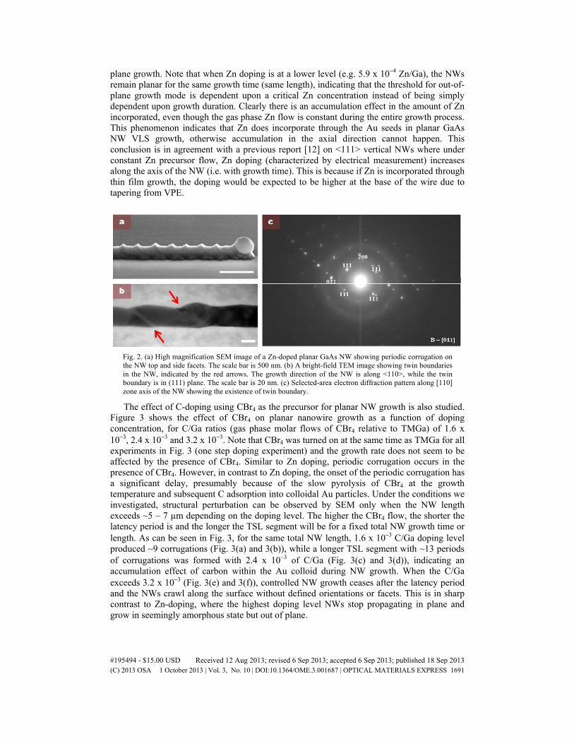
plane growth. Note that when Zn doping is at a lower level (e.g. 5.9 x 10⁻⁴ Zn/Ga), the NWs remain planar for the same growth time (same length), indicating that the threshold for out-of-plane growth mode is dependent upon a critical Zn concentration instead of being simply dependent upon growth duration. Clearly there is an accumulation effect in the amount of Zn incorporated, even though the gas phase Zn flow is constant during the entire growth process. This phenomenon indicates that Zn does incorporate through the Au seeds in planar GaAs NW VLS growth, otherwise accumulation in the axial direction cannot happen. This conclusion is in agreement with a previous report [12] on <111> vertical NWs where under constant Zn precursor flow, Zn doping (characterized by electrical measurement) increases along the axis of the NW (i.e. with growth time). This is because if Zn is incorporated through thin film growth, the doping would be expected to be higher at the base of the wire due to tapering from VPE.
Fig. 2. (a) High magnification SEM image of a Zn-doped planar GaAs NW showing periodic corrugation on the NW top and side facets. The scale bar is 500 nm. (b) A bright-field TEM image showing twin boundaries in the NW, indicated by the red arrows. The growth direction of the NW is along <110>, while the twin boundary is in (111) plane. The scale bar is 20 nm. (c) Selected-area electron diffraction pattern along [110] zone axis of the NW showing the existence of twin boundary.
The effect of C-doping using CBr4 as the precursor for planar NW growth is also studied. Figure 3 shows the effect of CBr4 on planar nanowire growth as a function of doping concentration, for C/Ga ratios (gas phase molar flows of CBr4 relative to TMGa) of 1.6 x 10⁻³, 2.4 x 10⁻³ and 3.2 x 10⁻³. Note that CBr4 was turned on at the same time as TMGa for all experiments in Fig. 3 (one step doping experiment) and the growth rate does not seem to be affected by the presence of CBr4. Similar to Zn doping, periodic corrugation occurs in the presence of CBr4. However, in contrast to Zn doping, the onset of the periodic corrugation has a significant delay, presumably because of the slow pyrolysis of CBr4 at the growth temperature and subsequent C adsorption into colloidal Au particles. Under the conditions we investigated, structural perturbation can be observed by SEM only when the NW length exceeds ~5 – 7 µm depending on the doping level. The higher the CBr4 flow, the shorter the latency period is and the longer the TSL segment will be for a fixed total NW growth time or length. As can be seen in Fig. 3, for the same total NW length, 1.6 x 10⁻³ C/Ga doping level produced ~9 corrugations (Fig. 3(a) and 3(b)), while a longer TSL segment with ~13 periods of corrugations was formed with 2.4 x 10⁻³ of C/Ga (Fig. 3(c) and 3(d)), indicating an accumulation effect of carbon within the Au colloid during NW growth. When the C/Ga exceeds 3.2 x 10⁻³ (Fig. 3(e) and 3(f)), controlled NW growth ceases after the latency period and the NWs crawl along the surface without defined orientations or facets. This is in sharp contrast to Zn-doping, where the highest doping level NWs stop propagating in plane and grow in seemingly amorphous state but out of plane.
#195494 - $15.00 USD Received 12 Aug 2013; revised 6 Sep 2013; accepted 6 Sep 2013; published 18 Sep 2013(C) 2013 OSA 1 October 2013 | Vol. 3, No. 10 | DOI:10.1364/OME.3.001687 | OPTICAL MATERIALS EXPRESS 1691
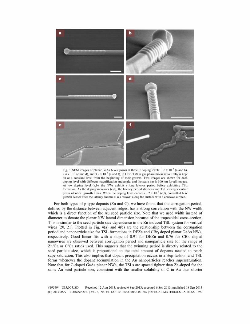
Fig. 3. SEM images of planar GaAs NWs grown at three C doping levels: 1.6 x 10⁻³ (a and b), 2.4 x 10⁻³ (c and d), and 3.2 x 10⁻³ (e and f), in CBr4/TMGa gas phase molar ratio. CBr4 is kept on at a constant level from the beginning of their growth. Two images are shown for each doping level with different magnification and angle, and the scale bar is 500 nm for all images. At low doping level (a,b), the NWs exhibit a long latency period before exhibiting TSL formation. As the doping increases (c,d), the latency period shortens and TSL emerges earlier given identical growth times. When the doping level exceeds 3.2 x 10⁻³ (e,f), controlled NW growth ceases after the latency and the NWs ‘crawl’ along the surface with a concave surface.
For both types of p-type dopants (Zn and C), we have found that the corrugation period, defined by the distance between adjacent ridges, has a strong correlation with the NW width which is a direct function of the Au seed particle size. Note that we used width instead of diameter to denote the planar NW lateral dimension because of the trapezoidal cross-section. This is similar to the seed particle size dependence in the Zn induced TSL system for vertical wires [20, 21]. Plotted in Fig. 4(a) and 4(b) are the relationship between the corrugation period and nanoparticle size for TSL formations in DEZn and CBr4 doped planar GaAs NWs, respectively. Good linear fits with a slope of 0.91 for DEZn and 0.76 for CBr4 doped nanowires are observed between corrugation period and nanoparticle size for the range of Zn/Ga or C/Ga ratios used. This suggests that the twinning period is directly related to the seed particle size, which is proportional to the total amount of dopants needed to reach supersaturation. This also implies that dopant precipitation occurs in a step fashion and TSL forms whenever the dopant accumulation in the Au nanoparticles reaches supersaturation. Note that for C-doped GaAs planar NWs, the TSLs are spaced tighter than Zn-doped for the same Au seed particle size, consistent with the smaller solubility of C in Au thus shorter
#195494 - $15.00 USD Received 12 Aug 2013; revised 6 Sep 2013; accepted 6 Sep 2013; published 18 Sep 2013(C) 2013 OSA 1 October 2013 | Vol. 3, No. 10 | DOI:10.1364/OME.3.001687 | OPTICAL MATERIALS EXPRESS 1692

accumulation period before precipitation. Mapping the Zn or C impurity distribution in the NWs will be critical in order to verify the doping incorporation mechanism in these planar NWs.
Fig. 4. Relationship between corrugation period (distance between adjacent notches as shown in the inset SEM image) and Au nanoparticle size for (a) Zn-doped and (b) C-doped planar GaAs nanowires. Linear fits with slopes of 0.91 for DEZn and 0.76 for CBr4 doped NWs are found over a wide range of Au seed particle sizes for several doping levels.
In addition to perturbing the NW growth using dopant impurities from the gas phase, we have also performed experiments where Zn or C impurities originate from either the substrates or Au seed particles. It is well known that Zn is highly diffusive in GaAs at elevated temperatures. Au nanoparticles can getter Zn impurities from the GaAs substrate during desorption and growth processes. As shown in Fig. 5, corrugated faceting can be clearly seen when grown on a highly Zn-doped (> 5x1019 cm-3) GaAs (100) wafer after a short latency period. This indicates that the characteristic corrugation morphology is the signature of Zn incorporation in GaAs through Au catalyst nanoparticles, regardless of the source of Zn. The observation of a latency period here before periodic corrugation proves that
Fig. 5. Tilted SEM image showing the appearance of periodic corrugations (indicated by arrows) after a short latency period (smooth morphology) in planar GaAs NWs, grown on a heavily Zn-doped (5x1019 cm−3) GaAs epilayer from randomly dispersed Au seed particles. The scale bar is 1 μm.
#195494 - $15.00 USD Received 12 Aug 2013; revised 6 Sep 2013; accepted 6 Sep 2013; published 18 Sep 2013(C) 2013 OSA 1 October 2013 | Vol. 3, No. 10 | DOI:10.1364/OME.3.001687 | OPTICAL MATERIALS EXPRESS 1693
such latency is not unique to carbon doping. We attribute the latency period here (the smooth
morphology segment) to the time necessary to adsorb Zn from the substrate and accumulate in the Au seed particles before Zn incorporation related morphology change takes place. Note that undoped and low level (1x1018 cm3) Zn-doped GaAs wafers loaded in the same growth run did not produce the characteristic corrugated morphology, presumably because the Zn concentration threshold for twinning was not reached for the growth period (100 seconds) examined. We do not believe that Zn diffusion directly into the planar GaAs NWs from the substrate is significant at such low growth temperature (~460°C) and does not play a role in the NW morphology because the NW growth front is at the Au seed and NW interface.
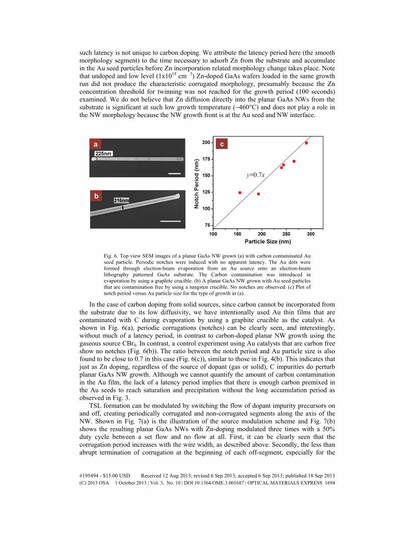
Fig. 6. Top view SEM images of a planar GaAs NW grown (a) with carbon contaminated Au seed particle. Periodic notches were induced with no apparent latency. The Au dots were formed through electron-beam evaporation from an Au source onto an electron-beam lithography patterned GaAs substrate. The Carbon contamination was introduced in evaporation by using a graphite crucible. (b) A planar GaAs NW grown with Au seed particles that are contamination free by using a tungsten crucible. No notches are observed. (c) Plot of notch period versus Au particle size for the type of growth in (a).
In the case of carbon doping from solid sources, since carbon cannot be incorporated from the substrate due to its low diffusivity, we have intentionally used Au thin films that are contaminated with C during evaporation by using a graphite crucible as the catalyst. As shown in Fig. 6(a), periodic corrugations (notches) can be clearly seen, and interestingly, without much of a latency period, in contrast to carbon-doped planar NW growth using the gaseous source CBr4. In contrast, a control experiment using Au catalysts that are carbon free show no notches (Fig. 6(b)). The ratio between the notch period and Au particle size is also found to be close to 0.7 in this case (Fig. 6(c)), similar to those in Fig. 4(b). This indicates that just as Zn doping, regardless of the source of dopant (gas or solid), C impurities do perturb planar GaAs NW growth. Although we cannot quantify the amount of carbon contamination in the Au film, the lack of a latency period implies that there is enough carbon premixed in the Au seeds to reach saturation and precipitation without the long accumulation period as observed in Fig. 3.
TSL formation can be modulated by switching the flow of dopant impurity precursors on and off, creating periodically corrugated and non-corrugated segments along the axis of the NW. Shown in Fig. 7(a) is the illustration of the source modulation scheme and Fig. 7(b) shows the resulting planar GaAs NWs with Zn-doping modulated three times with a 50% duty cycle between a set flow and no flow at all. First, it can be clearly seen that the corrugation period increases with the wire width, as described above. Secondly, the less than abrupt termination of corrugation at the beginning of each off-segment, especially for the
#195494 - $15.00 USD Received 12 Aug 2013; revised 6 Sep 2013; accepted 6 Sep 2013; published 18 Sep 2013(C) 2013 OSA 1 October 2013 | Vol. 3, No. 10 | DOI:10.1364/OME.3.001687 | OPTICAL MATERIALS EXPRESS 1694
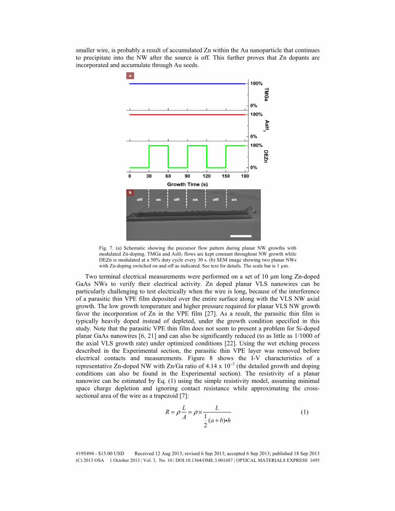
smaller wire, is probably a result of accumulated Zn within the Au nanoparticle that continues to precipitate into the NW after the source is off. This further proves that Zn dopants are incorporated and accumulate through Au seeds.
Fig. 7. (a) Schematic showing the precursor flow pattern during planar NW growths with modulated Zn-doping. TMGa and AsH3 flows are kept constant throughout NW growth while DEZn is modulated at a 50% duty cycle every 30 s. (b) SEM image showing two planar NWs with Zn-doping switched on and off as indicated. See text for details. The scale bar is 1 µm.
Two terminal electrical measurements were performed on a set of 10 μm long Zn-doped GaAs NWs to verify their electrical activity. Zn doped planar VLS nanowires can be particularly challenging to test electrically when the wire is long, because of the interference of a parasitic thin VPE film deposited over the entire surface along with the VLS NW axial growth. The low growth temperature and higher pressure required for planar VLS NW growth favor the incorporation of Zn in the VPE film [27]. As a result, the parasitic thin film is typically heavily doped instead of depleted, under the growth condition specified in this study. Note that the parasitic VPE thin film does not seem to present a problem for Si-doped planar GaAs nanowires [6, 21] and can also be significantly reduced (to as little as 1/1000 of the axial VLS growth rate) under optimized conditions [22]. Using the wet etching process described in the Experimental section, the parasitic thin VPE layer was removed before electrical contacts and measurements. Figure 8 shows the I-V characteristics of a representative Zn-doped NW with Zn/Ga ratio of 4.14 x 10⁻³ (the detailed growth and doping conditions can also be found in the Experimental section). The resistivity of a planar nanowire can be estimated by Eq. (1) using the simple resistivity model, assuming minimal space charge depletion and ignoring contact resistance while approximating the cross-sectional area of the wire as a trapezoid [7]:
1
( )2
L LRA a b h
ρ ρ= = ×+
(1)
#195494 - $15.00 USD Received 12 Aug 2013; revised 6 Sep 2013; accepted 6 Sep 2013; published 18 Sep 2013(C) 2013 OSA 1 October 2013 | Vol. 3, No. 10 | DOI:10.1364/OME.3.001687 | OPTICAL MATERIALS EXPRESS 1695

where R is resistance, ρ is resistivity, A is the NW cross-section area, L (7 μm) is the length of the NW, a (92 nm) and b (231 nm) are the widths of the NW top and bottom facets, and h (98 nm) is the NW height, as determined by planar GaAs NW geometry [23]. The NW resistivity (lower limit since depletion width is ignored) is then calculated to be on the order of 10−3 Ω·cm, which corresponds to a Zn doping concentration of ~7x1019 cm−3 based on the empirical curves for VPE films in literature [24]. On the other hand, for all attempted electrical testing of C doped GaAs NWs, no electrical activity was measurable, indicating a doping level lower than ~1 x 1017 cm−3 considering the NW width and depletion depth. This is probably due to the low solubility of C in Au [25].Note that there was also no detectable highly doped VPE parasitic thin film under our C-doping condition, in contrast to what has been previously reported [26].
Fig. 8. Two terminal IV characteristics of Zn-doped planar GaAs NW (black solid trace) grown on a GaAs (100) substrate with a Zn/Ga ratio of 4.14 x 10⁻³. Substrate leakage (red dashed line) is negligible after removing the parasitic VPE film.
TSL formation in vertical NWs has been reported in several binary III-V systems such as InAs [27], GaP [28] and InP NWs [20], induced by adjusting temperature, impurity doping, or V/III ratio [29] during NW growth. Polytypic growth, switching between crystal structures (typically wurtzite and zinc blende), has also been reported in conjunction with TSL formation. This is the first report on TSLs in planar NWs. TSLs in planar nanowires induced by p-type dopant impurities have similar basic properties with their vertically oriented counterparts: twin planes coincide with (111) crystal growth planes; formation of TSL is responsive to growth and doping conditions; and the NW diameter affects twin lattice spacing. However, there are pronounced differences arising from the inherent geometry of planar NWs. First, the TSL plane is no longer orthogonal to the NW axial direction for planar NWs. This is because the growth plane, consequently the twin planes, is (111)B which forms a 35.3° intersection with the <110> crystal direction, the planar NW propagation direction on GaAs (100) substrates. The non-orthogonality of growth and propagation directions, and epitaxial attachment to the surface leads to a cross-section and outward surface faceting that are different from those for vertical <111>B III-V NWs [30]. Secondly, while the twinning is highly periodic in planar NWs, in contrast to the vertical counterparts, the non-twinned and twinned segments are far from equal in length (twinned segment is significantly shorter) based on TEM examinations. As a result, the effect of NW diameter/width on the twin plane lattice spacing is qualitatively the same trend but quantitatively different. Algra et al. proposed a model that relates the periodic twinning to the minimization of Au seed surface area and liquid-solid interface energy during NW growth [20]. This implies that in planar
#195494 - $15.00 USD Received 12 Aug 2013; revised 6 Sep 2013; accepted 6 Sep 2013; published 18 Sep 2013(C) 2013 OSA 1 October 2013 | Vol. 3, No. 10 | DOI:10.1364/OME.3.001687 | OPTICAL MATERIALS EXPRESS 1696
NWs the twinned segments becoming energetically unfavorable at a shorter segment length than the untwined (defect-free) segments. The difference is likely because of the unique planar NW geometry and epitaxial nature of the planar NWs. Likewise, polytypism in planar GaAs NWs has not been observed, probably due to their epitaxial relationship along the NW axis with the zinc-blende crystalline substrate. Lastly, the onset of TSL formation in planar Zn-doped GaAs NWs is around 1019 cm−3 doping level based on our electrical testing results and assuming a linear incorporation relationship. In contrast, for vertical Zn-doped InP NWs reported in [20], the onset of the first phase transition from wurtzite to zinc-blende (no equivalent transition in planar NWs) started at 1018 cm−3 followed by the appearance of TSLs at one order of magnitude higher in Zn partial pressure (similar to that of planar NWs). It will be interesting to see if the onset of these TSLs can be delayed by varying the growth conditions to obtain highly doped III-V NWs that are defect-free.
4. Conclusion
In conclusion, we have reported the effect of Zn and C doping on the VLS growth of planar GaAs NWs. At a constant flow of dopant to Ga precursor gas phase molar ratio as low as 5.9 x 10⁻⁴, periodic corrugations along the planar NW top facets are formed. The corrugated ridges correspond to <111> TSL defects and the corrugation period is strongly correlated with the Au seed particle size. In contrast to Zn-doping, the appearance of TSLs caused by C-doping has a long latency period, which shortens with increasing C doping level. All evidence points to the incorporation of these dopants through the Au seed particles instead of sidewalls. The characteristic corrugation or TSL formation serves as a signature of mid to high level p-type doping and can be turned on and off by switching the dopants in and out, as well as modulated with Si-doing for in situ lateral p-n junction formation. The unique topography of the TSL based planar NW structures will inevitably affect the electronic band structure, phonon scattering, as well as local optical index contrast. Combining with the processing advantages of planar NW geometry, TSL based planar NW structures could lead to new concepts in novel photonic and thermal devices.
Acknowledgment
Part of this work was previously presented at the 2012 IEEE Photonics Society meeting. Financial support was provided by NSF DMR #1006581.
#195494 - $15.00 USD Received 12 Aug 2013; revised 6 Sep 2013; accepted 6 Sep 2013; published 18 Sep 2013(C) 2013 OSA 1 October 2013 | Vol. 3, No. 10 | DOI:10.1364/OME.3.001687 | OPTICAL MATERIALS EXPRESS 1697