perovskite thin film solar cells based on inorganic hole...
TRANSCRIPT

HindawiInternational Journal of PhotoenergyVolume 2017, Article ID 6109092, 10 pageshttps://doi.org/10.1155/2017/6109092
Review ArticlePerovskite Thin Film Solar Cells Based on Inorganic HoleConducting Materials
Pan-Pan Zhang,1,2 Zheng-Ji Zhou,1,2 Dong-Xing Kou,1,2 and Si-Xin Wu1,2
1Key Laboratory for Special Functional Materials of Ministry of Education, Henan University, Kaifeng,Henan Province 475004, China2Collaborative Innovation Center of Nano Functional Materials and Applications, Henan University, Kaifeng,Henan Province 475004, China
Correspondence should be addressed to Zheng-Ji Zhou; [email protected]
Received 13 October 2016; Revised 14 February 2017; Accepted 23 February 2017; Published 3 May 2017
Academic Editor: Wilfried G.J.H.M. Van Sark
Copyright © 2017 Pan-Pan Zhang et al. This is an open access article distributed under the Creative Commons Attribution License,which permits unrestricted use, distribution, and reproduction in any medium, provided the original work is properly cited.
Organic-inorganic metal halide perovskites have recently shown great potential for application, due to their advantages of low-cost,excellent photoelectric properties and high power conversion efficiency. Perovskite-based thin film solar cells have achieved apower conversion efficiency (PCE) of up to 20%. Hole transport materials (HTMs) are one of the most important componentsof perovskite solar cells (PSCs), having functions of optimizing interface, adjusting the energy match, and helping to obtainhigher PCE. Inorganic p-type semiconductors are alternative HTMs due to their chemical stability, higher mobility, hightransparency in the visible region, and applicable valence band (VB) energy level. This review analyzed the advantages,disadvantages, and development prospects of several popular inorganic HTMs in PSCs.
1. Introduction
Perovskite solar cells (PSCs) based on organic-inorganicmetal halide perovskites have recently attracted considerableattention as the power conversion efficiency (PCE) hasincreased dramatically from the initial 3.9% in 2009 tocurrent 22.1% in a short span of several years [1–8]. Previousresults demonstrated that PSCs may be the first in the historyof photovoltaics (PV) combining high efficiency with lowcost. The configurations of PSCs were evolved from dye-sensitized solar cells (DSSCs), and the key materials forthe perovskite are compounds with the chemical formulaABX3 (A = CH3NH3, B = Pb or Sn, and X = Cl, Br, or I),which have received extensive attention due to their favorablephotovoltaic properties [9, 10]. Generally, the device structureof PSCs can be categorized into mesoporous structure(Figure 1(a)) and planar junction structure (Figure 1(b)) [11].Themain function of perovskite is absorbing light to generateand transmit electron-hole pairs under continuous illumina-tion. Then, the electrons and holes pass through the perov-skite and shift to electron-transporting layer (ETL) and
hole transport layer (HTL), respectively, to generatecurrent, as schematic presented in Figure 1(c).
While although a mass of efforts such as solvent addi-tives, molecular dipoles, or interface modification has beendevoted to optimize device efficiency, none of the presentPSCs provides high PCE with long-term stability. Undoubt-edly, a lack of confirmed stability may become the biggestbarrier on the path of PSCs towards commercialization.HTL is one of the most important components of PSCs,having functions of optimizing interface, adjusting theenergy-match, and helping obtain higher PCE, whichhas a great effect on device performance and stability[12–14]. Poly(3,4-ethylenedioxythiophene)-polystyrenesul-fonate (PEDOT:PSS) and2,2′,7,7′-tetrakis (N,N-di-p-methox-yphenylamine)-9,9,-spirobifluorene (spiro-OMeTAD) havebeen widely employed as HTL in the field of PSCs. AlthoughPSCs that applied PEDOT:PSS and spiro-OMeTAD asHTL have obtained high PCE, none of them can providewith long-term stability partly because of the problematicacidic and hygroscopic characteristics of the organic HTMsapplied in PSCs [15, 16].

GlassTCO
N‒contact
Mesoporous NPs/peroviskite
P‒contactMetal
GlassTCO
N‒contact
Peroviskite
P‒contactMetal
HTM
TCO
subs
trat
e
Met
al el
ectro
de
ETMSensitizer
e‒
h+
(a) (b) (c)
Figure 1: Device structures of (a) mesoporous structure, (b) n–i–p planar, planar junction structure, and (c) the scheme of carriertransport in PSCs.
Table 1: Device parameters for high-performance organometallic lead halide perovskite solar cells (PSCs) based on different inorganic holetransport materials (HTMs), the band gap, and deposition method of these HTMs.
HTM Band gap (eV) Deposition method Voc (V) Jsc (mA/cm2) FF (%) PCE (%) Reference
NiO 3.5 ALD 1.04 21.87 72 16.40 [37]
Cu:NiO x> 3.5 Solution-processed 1.12 19.17 73 15.40 [24]
Mg:Li:NiO x> 3.5 Solution-processed 1.07 20.62 75 18.40 [36]
CuI 3.1 Solution-processed 1.04 21.06 62 13.58 [40]
CuSCN 3.8 Electrodeposition 1.00 21.90 76 16.60 [46]
CuO 1.3 Solution-processed 1.06 15.82 72 12.16 [52]
Cu2O 2.1 Solution-processed 1.07 16.52 75 13.35 [52]
MoO3 3.4 Thermal decomposition 1.00 21.49 69 14.87 [53]
VOx 2.42 Solution-processed 0.90 22.29 71 14.23 [55]
2 International Journal of Photoenergy
Recently, to improve the stability and reduce the cost ofPSCs, various inorganic hole transport materials have beendiscovered and applied. In this review, PSCs employingdifferent inorganic HTMs as hole transport layer (HTL) havebeen discussed and summarized. To date, a series of p-typeinorganic metal compounds have been employed in PSCs,such as CuI [17], CuSCN [18–20], NiO [21–26], CuO [27],Cu2O [27, 28], MoO3 [29–31], and VOx [32]. Compared toorganic HTMs, inorganic p-type semiconductor materialshave the advantages of high hole mobility, wide band gap,low cost, and solution-processed availability, which showpromising prospects as hole-selective contacts in perovskitesolar cells.
2. Inorganic HTMs for PSCs
There are some general requirements for inorganic HTMsused in PSCs, such as high transparency in the visibleregion, well chemical stability, higher mobility, and appli-cable valence band (VB) energy level. At present, inorganicHTMs such as CuI, CuSCN, NiO, CuO, Cu2O, MoO3, andVOx have already been used in PSCs and the solar cellsemploying inorganic p-type semiconductors as HTLs exhib-ited improvement in device performance and stability.
Table 1 presents the band gap and deposition method ofvarious HTMs reported in the literatures, as well as theirphotovoltaic parameters of top-performing PSCs based onthese HTMs. In the following, we will analyze and discussthese frequently used inorganic HTMs, respectively.
2.1. NiO. NiO is a well-known p-type semiconductorwidely used as a p-sensitization electrode for DSSCs anda hole-selective contact for organic bulk heterojunctionsolar cells [33, 34].
Initially, NiO was widely applied in DSSCs. In recentyears, nickel oxide (NiO) as a promising HTM has beenstudied by several groups. In 2014, the first announced PCEof PSCs using nickel oxide as HTL was up to 7.8% [35]. Then,NiO nanocrystals (NCs) were obtained by a simple sol-gelprocess adopted as the hole transport layer in an invertedPSC, which observed a high PCE of 9.11% [25]. In 2015,copper- (Cu-) doped NiO (Cu:NiO) as HTL of planarheterojunction PSCs achieved a PCE of 15.4% [24]. Atpresent, the highest recorded PCE of PSCs using Li, Mg-codoped NiO (Li0.05Mg0.15Ni0.8O) as HTL was 18.4% [36].This study developed heavily p-doped (p+) NixMg1–xO toextract photogenerated hole from perovskite layer, and largesize (>1 cm2) PSCs with an efficiency of up to 16.2% were

(a) (b)
60 nm
0 nm
(c)
Figure 2: (a) SEM NiO film prepared by spin coating, (b) and (c) AFM of NiO film prepared by spin coating. Reprinted withpermission from [21].
Inte
nsity
(a.u
.)
Wavelength (nm)720
CH3NH3Pbl3/quartzCH3NH3Pbl3/NiO/quartz
740 760 780 800
Figure 3: Photoluminescence spectra (excited by 600 nm laser) ofCH3NH3PbI3 film deposited on top of NiO film or quartzsubstrate. Reprinted with permission from [21].
3International Journal of Photoenergy
successfully fabricated. The latest reported PCE of PSCsemploying pure NiO as HTL is up to 16.4%, and the NiOfilm was gotten by the atomic layer deposition (ALD)method [37].
NiO become a potential candidate for HTL, as its p-typecharacteristics of high optical transmittance, wide band gap(Eg> 3.50 eV), chemical stability, and an applicable valenceband match with common light photoactive layers [33, 38].The synthetic methods of NiO can be categorized intosolution-processed and sol-gel, and NiO films can be pre-pared by various methods, such as pulsed laser deposition,electrodeposition, spray pyrolysis, spin coating, sputtering,and ALD method [37]. A frequently used method for pre-paring NiO is solution-processed technique by addingmonoethanolamine and nickel acetate tetrahydrate in meth-oxyethanol then stirring for 10 hours to form NiO precursorsolutions and via spin coating to achieve NiO film. TheNiO film obtained by this way was composed of NiOnanoparticles (NCs), and the whole film was crack-freeand smooth, as schematic presented in SEM and AFM(Figures 2(a), 2(b), and 2(c)). The photoluminescence(PL) quenching of perovskite based on NiO showed favorablecharge transfer compatibility, presented in Figure 3. Perov-skite excitation is at around 760 nm. Finally, PSC with NiOprepared by the above method as HTL obtained a 7.6%device performance [21].
Another common approach to achieve NiO is a simplesol-gel process. NiO film was fabricated by spin coating thesol-gel solution. This kind of NiO nanocrystal film with a flatand smooth surface guarantees the formation of a continuousand close-knit HTLs of PSCs as schematic presented inFigures 4(a) and 4(b). Hole extraction and transport proper-ties of this film interfaced with the perovskite film were
higher than those of organic HTLs, such as PEDOT:PSS,and perovskite deposited on NiO NC films is with homoge-neous phase. The PSCs with HTL of NiO NC film at athickness of around 35nm exhibited the best PCE of 9.11%,as showed in Figure 4(c) [25].
Recently, ALD method has been used to fabricateultrathin pure un-doped NiO films. And PSCs employingthis kind of NiO film as HTL achieved a high PCE of16.4%. We can fabricate highly sequential and dense ultra-thin films at nanometer size following the ALD method.

200 nm
6 nm
‒6 nm
200 nm
(a) (b)
18
16
1412
10
864
2
00.0
NiO NCs—20 nmNiO NCs—40 nmNiO NCs—70 nm
NiO thin filmPEDOT:PSS
0.40.2Voltage (V)
Curr
ent d
ensit
y (m
A cm
‒2)
0.6 0.8 1.0
(c)
Figure 4: (a) AFM roughness image of a NiO nanocrystal film on FTO. (b) Bright-field TEM image of a sample of NiO NCs with thecorresponding diffraction pattern (inset). (c) Typical J–V curves of the perovskite solar cells with different NiO hole transport layers andPEDOT:PSS. Reprinted with permission from [25].
100
PEDOT:PSSCuI
80
60
40
20
0300 400 500
Wavelength (nm)
Tran
smitt
ance
(%)
600 700 800
Figure 5: Optical transmission spectra of the PEDOT:PSS film andCuI film. Reprinted with permission from [40].
4 International Journal of Photoenergy
The effective work function (WF) of ultrathin NiO appar-ently increased, which enormously promoted the holeextraction performance. In addition, ultrathin NiO filmshave a higher transparency which highly contribute to thephotovoltaic devices. The freshly ultrathin pure undopedNiO films deposited as HTL of PSCs exhibited a highPCE of 16.4% with Jsc = 21 9mA cm−2, Voc = 1 04V, andFF = 0 72 [37].
A salient weakness with PSCs’ use of NiO as HTL is thatit is hard for NiO to support an ultrathin perovskite film(<60nm) [22, 23], which has still limited the developmentof PCE of PSCs using NiO as HTLs. Another shortage withPSCs employing NiO as HTL is that FF and Voc are lowerthan the common organic HTMs, in particular when theNiO was achieved by the solution-processed method. Theseparameters greatly affect the device performance [37].
Briefly speaking, an ideal p-NiO film for high PV per-formance should (1) have high transparency, (2) have favor-able hole extraction and transport performance properties,
1.0
0.8
0.6
0.4
Nor
mal
ized
PCE
Time (h)
0.2
0.00 50 100 150 200 250 300 350
1.0
0.8
0.6
0.4
Nor
mal
ized
Voc
Time (h)
0.2
0.00 50 100 150 200 250 300 350
(a) (b)
PEDOT:PSSCuI
1.0
0.8
0.6
0.4
Nor
mal
ized
Jsc
Time (h)
0.2
0.00 50 100 150 200 250 300 350
1.0
0.8
0.6
0.4N
orm
aliz
ed P
CE
Time (h)
0.2
0.00 50 100 150 200 250 300 350
PEDOT:PSSCuI
(c) (d)
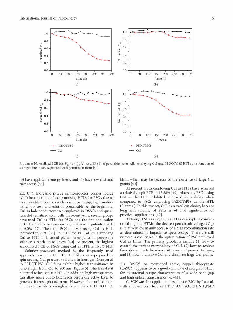
Figure 6: Normalized PCE (a), Voc (b), Jsc (c), and FF (d) of perovskite solar cells employing CuI and PEDOT:PSS HTLs as a function ofstorage time in air. Reprinted with permission from [40].
5International Journal of Photoenergy
(3) have applicable energy levels, and (4) have low cost andeasy access [33].
2.2. CuI. Inorganic p-type semiconductor copper iodide(CuI) becomes one of the promising HTLs for PSCs, due toits admirable properties such as wide band gap, high conduc-tivity, low cost, and solution processable. At the beginning,CuI as hole conductors was employed in DSSCs and quan-tum dot-sensitized solar cells. In recent years, several groupshave used CuI as HTLs for PSCs, and the first applicationof CuI for PSCs has successfully achieved a potential PCEof 6.0% [17]. Then, the PCE of PSCs using CuI as HTLincreased to 7.5% [39]. In 2015, the PCE of PSCs applyingCuI as HTL in inverted planar heterojunction perovskitesolar cells reach up to 13.8% [40]. At present, the highestannounced PCE of PSCs using CuI as HTL is 16.8% [41].
Solution-processed method is the frequently usedapproach to acquire CuI. The CuI films were prepared byspin coating CuI precursor solution in inert gas. Comparedto PEDOT:PSS, CuI films exhibit higher transmittance invisible light from 450 to 800nm (Figure 5), which make itpotential to be used as a HTL. In addition, high transparencycan allow more photo flux reach perovskite active layer togenerate intense photocurrent. However, the surface mor-phology of CuI films is rough when compared to PEDOT:PSS
films, which may be because of the existence of large CuIgrains [40].
At present, PSCs employing CuI as HTLs have achieveda relatively high PCE of 13.58% [40]. Above all, PSCs usingCuI as the HTL exhibited improved air stability whencompared to PSCs employing PEDOT:PSS as the HTL(Figure 6). In this respect, CuI is an excellent choice, becauselong-term stability of PSCs is of vital significance forpractical applications [40].
Although PSCs using CuI as HTLs can replace conven-tional organic HTMs, the device open-circuit voltage (Voc)is relatively low mainly because of a high recombination rateas determined by impedance spectroscopy. There are stillnumerous challenges in the optimization of PSC-employedCuI as HTLs. The primary problems include (1) how tocontrol the surface morphology of CuI, (2) how to achievefavorable contacts between CuI layer and perovskite layer,and (3) how to dissolve CuI and eliminate large CuI grains.
2.3. CuSCN. As mentioned above, copper thiocyanate(CuSCN) appears to be a good candidate of inorganic HTLsfor its internal p-type characteristics of a wide band gapand high optical transparency [42–44].
CuSCN was first applied in mesoporous PSCs by Ito et al.with a device structure of FTO/TiO2/TiO2/CH3NH3PbI3/
0
020
(nm
)
1 2 3 4 5
43
21
0
(�휇m)
0
010
0(n
m)
1 2 3 4 5
43
21
0
(�휇m)
(a) (b)
0
050
(nm
)
1 2 3 4 5
43
21
0
(�휇m)
00
100
(nm
)1 2 3 4 5
43
21
0
(�휇m)
(c) (d)
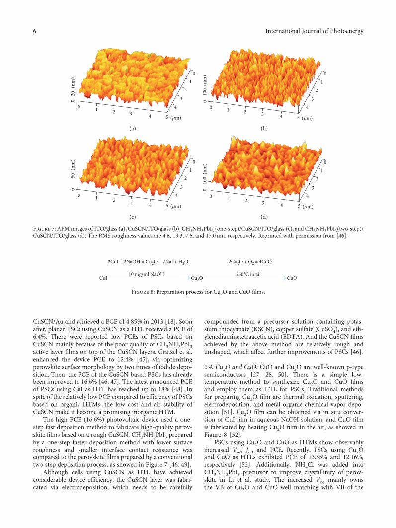
Figure 7: AFM images of ITO/glass (a), CuSCN/ITO/glass (b), CH3NH3PbI3 (one-step)/CuSCN/ITO/glass (c), and CH3NH3PbI3(two-step)/CuSCN/ITO/glass (d). The RMS roughness values are 4.6, 19.3, 7.6, and 17.0 nm, respectively. Reprinted with permission from [46].
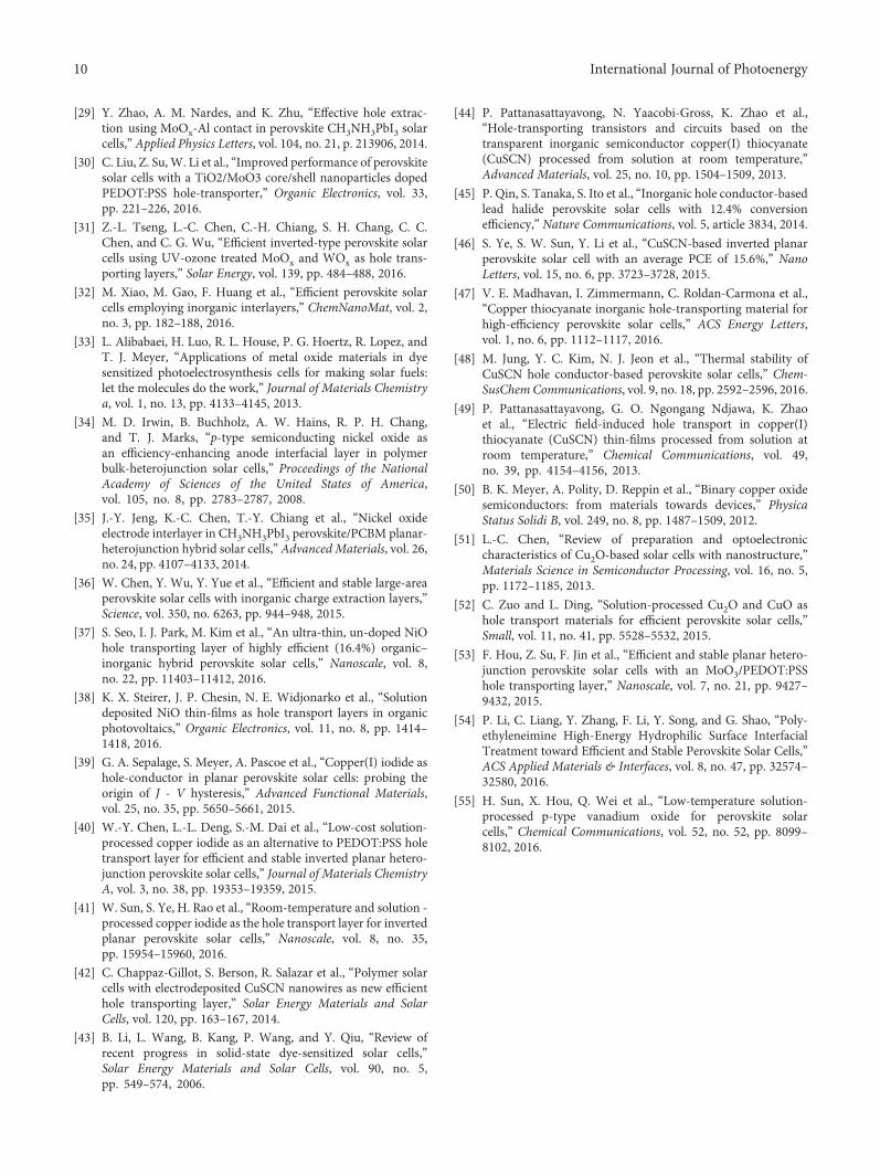
2CuI + 2NaOH = Cu2O + 2NaI + H2O 2Cu2O + O2 = 4CuO
CuI Cu2O CuO10 mg/ml NaOH 250°C in air
Figure 8: Preparation process for Cu2O and CuO films.
6 International Journal of Photoenergy
CuSCN/Au and achieved a PCE of 4.85% in 2013 [18]. Soonafter, planar PSCs using CuSCN as a HTL received a PCE of6.4%. There were reported low PCEs of PSCs based onCuSCN mainly because of the poor quality of CH3NH3PbI3active layer films on top of the CuSCN layers. Grätzel et al.enhanced the device PCE to 12.4% [45], via optimizingperovskite surface morphology by two times of iodide depo-sition. Then, the PCE of the CuSCN-based PSCs has alreadybeen improved to 16.6% [46, 47]. The latest announced PCEof PSCs using CuI as HTL has reached up to 18% [48]. Inspite of the relatively low PCE compared to efficiency of PSCsbased on organic HTMs, the low cost and air stability ofCuSCN make it become a promising inorganic HTM.
The high PCE (16.6%) photovoltaic device used a one-step fast deposition method to fabricate high-quality perov-skite films based on a rough CuSCN. CH3NH3PbI3 preparedby a one-step faster deposition method with lower surfaceroughness and smaller interface contact resistance wascompared to the perovskite films prepared by a conventionaltwo-step deposition process, as showed in Figure 7 [46, 49].
Although cells using CuSCN as HTL have achievedconsiderable device efficiency, the CuSCN layer was fabri-cated via electrodeposition, which needs to be carefully
compounded from a precursor solution containing potas-sium thiocyanate (KSCN), copper sulfate (CuSO4), and eth-ylenediaminetetraacetic acid (EDTA). And the CuSCN filmsachieved by the above method are relatively rough andunshaped, which affect further improvements of PSCs [46].
2.4. Cu2O and CuO. CuO and Cu2O are well-known p-typesemiconductors [27, 28, 50]. There is a simple low-temperature method to synthesize Cu2O and CuO filmsand employ them as HTL for PSCs. Traditional methodsfor preparing Cu2O film are thermal oxidation, sputtering,electrodeposition, and metal-organic chemical vapor depo-sition [51]. Cu2O film can be obtained via in situ conver-sion of CuI film in aqueous NaOH solution, and CuO filmis fabricated by heating Cu2O film in the air, as showed inFigure 8 [52].
PSCs using Cu2O and CuO as HTMs show observablyincreased Voc, Jsc, and PCE. Recently, PSCs using Cu2Oand CuO as HTLs exhibited PCE of 13.35% and 12.16%,respectively [52]. Additionally, NH4Cl was added intoCH3NH3PbI3 precursor to improve crystallinity of perov-skite in Li et al. study. The increased Voc mainly ownsthe VB of Cu2O and CuO well matching with VB of the

(a)
(b)
(c)
(d)
25
20
15
10
5
1.00
0.95
0.90
0.85
0.75
0.70
0.65
0.60
0.55
15
10
5
00 50 100 150 200 250
J sc (m
A/c
m2 )
V oc (
V)
FFPC
E (%
)
Time (h)
0.2%0.5%1%
2%PEDOT:PSS
Figure 9: (a) Jsc, (b) Voc, (c) FF, and (d) PCE values as a function of aging time of the devices with different MoO3/PEDOT:PSS andpristine PEDOT:PSS HTLs. Reprinted with permission from [53].
7International Journal of Photoenergy
perovskite and favorable crystallinity of perovskite on Cu2Oand CuO. What is more, well crystallinity enhanced thecharge carrier transport and increased Jsc.
Compared to the PSCs employing NiO or Cu:NiO asHTLs, Cu2O-based cells showed a superior property due tothe higher mobility of Cu2O, less energy loss, and favorableperovskite surface morphology on Cu2O film [21].
2.5. MoO3. MoO3 is another potential HTM owing to theadvantage of nontoxicity and air stability. However, PSCswith MoO3 as HTL exhibit a low PCE mainly because of thepoor quality of perovskite films deposited on MoO3 [29, 31].
MoO3 is a good HTM, but the poor perovskite filmsdeposited on top of it limit further improvement. In orderto solve the difficult problem, one simple solution would beto use an MoO3/PEDOT:PSS composite film as the HTL inPSCs to take advantage of the ambient condition stabilityand favorable photovoltaic properties of MoO3 and at thesame time guarantee the admirable surface morphology ofperovskite film [53].
Li et al. used a MoO3/PEDOT:PSS bilayer structure asthe HTL for PSCs. MoO3 was prepared by a thermal decom-position of ammonium heptamolybdate ( NH4 6Mo7O24 −4H2O) solution at 80°C. The PSCs have a structure ofITO/MoO3/PEDOT:PSS/CH3NH3PbI3/C60/Bphen/Ag. Theapplication of an MoO3 layer between ITO and PEDOT:PSSnot only enhanced the hole extraction efficiency from perov-skite to the ITO electrode but also avoided direct contactbetween rough MoO3 and CH3NH3PbI3. By this way, wecan obtain a high-quality perovskite films deposited ontop of PEDOT:PSS. These improvements contribute to theincrease of stability and PCE of PSCs compared to the cellsemploying only PEDOT:PSS. Finally, the optimized PSCsexhibit a PCE of 14.87% [53]. What is more, the device stabil-ity increases when a MoO3 layer is inserted between ITO andPEDOT:PSS as showed in Figure 9 [53].
2.6. VOx. VOx has become a favorable p-type semiconductormaterial primarily due to its higher work function (WF)and stability, and it can be prepared by low-temperature

80°C
100
80
60
40
20300 400 500 600
Wavelength (nm)700 800 900
Tran
smitt
ance
(%)
120°C150°C
5.4
5.3
Wor
k fu
nctio
n (e
V)
5.2
5.1
5.0
80Annealing temperature (°C)
120 160 200
(a) (b)
31.6 nm
25.0
20.0
15.0
10.0
5.0
0.01 �휇m 1 �휇m
37.1 nm
30.0
20.0
25.0
15.0
10.0
5.0
0.0
(c) (d)
Figure 10: (a) Transmittance spectra of VOx layers annealed at different temperatures. (b) Work function of VOx layers annealed at differenttemperatures on ITO substrates. (c) AFM images of a bare ITO substrate. (d) AFM images of a VOx-coated ITO substrate. Reprinted withpermission from [55].
8 International Journal of Photoenergy
solution-processed method [32, 54]. At the beginning, VOxwas used as HTL in organic solar cells (OSCs). Recently,VOx occurred as HTL for PSCs and achieved a relativelyhigh PCE of 14.23% [55].
In general, VOx films are fabricated by spin coatingand annealed sol-gel precursor solution of VOx. And themeasurements of the VOx layer exhibit high transmittanceand well-quenching efficiency (Figure 10(a)). The value ofx in VOx was calculated at about 2.428 via X-ray photo-electron spectroscopy (XPS). High WF (Figure 10(b)) ofVOx not only extremely benefits cells containing high ion-ization potential donor materials but also reduces losses inVoc and series resistance (Rs) [55]. However, VOx is stillfaulty for it poor surface morphology result in harsh
deposition of perovskite films, as showed in Figures 10(c)and 10(d) [24, 45].
3. Conclusion
Inorganic semiconductor materials can be employed ashole-selective materials for PSCs due to their advantagesof high hole mobility, wide band gap, and low cost, andthey could be obtained by solution-processed method,showing promising respect of inorganic HTMs. What ismore, the application of inorganic HTMs can enormouslyincrease the stability and reduce cost of cells, which is verysignificant for PSCs. However, the reported device perfor-mance of most of the inorganic hole conductor-based PSCs

9International Journal of Photoenergy
is still much lower than that of cells with organic HTMs,which may result in the poor quality of perovskite films ontop of the inorganic HTL.
Conflicts of Interest
The authors declare that there is no conflict of interestregarding the publication of this paper.
Acknowledgments
The authors would like to thank the National Natural ScienceFoundation of China (21271064 and 61306016), ChinaPostdoctoral Science Foundation (2015M582179), and TheProgram for Changjiang Scholars and Innovative ResearchTeam in the University (PCS IRT1126) of Henan University.
References
[1] A. Kojima, K. Teshima, Y. Shirai, and T. Miyasaka, “Orga-nometal halide perovskites as visible-light sensitizers forphotovoltaic cells,” Journal of the American Chemical Soci-ety, vol. 131, no. 17, pp. 6050–6051, 2009.
[2] H. Zhou, Q. Chen, G. Li et al., “Interface engineering of highlyefficient perovskite solar cells,” Science, vol. 345, no. 6196,pp. 542–546, 2014.
[3] W. S. Yang, J. H. Noh, N. J. Jeon et al., “High-performancephotovoltaic perovskite layers fabricated through intramolecu-lar exchange,” Science, vol. 348, no. 6240, pp. 1234–1237, 2015.
[4] N. J. Jeon, J. H. Noh, W. S. Yang et al., “Compositionalengineering of perovskite materials for high-performance solarcells,” Nature, vol. 517, no. 7535, pp. 476–480, 2015.
[5] Z. Yu and L. Sun, “Recent progress on hole-transportingmaterials for emerging organometal halide perovskite solarcells,” Advanced Energy Materials, vol. 5, no. 12, 2015.
[6] S. Albrecht,M. Saliba, J. P. Baena et al., “Monolithic perovskite/silicon-heterojunction tandem solar cells processed at lowtemperature,” Energy & Environmental Science, vol. 9, no. 1,pp. 81–88, 2016.
[7] H. S. Jung and N.-G. Park, “Perovskite solar cells: frommaterials to devices,” Small, vol. 11, no. 1, pp. 10–25, 2015.
[8] “NREL efficiency chart,” June 2016, http://www.nrel.gov/ncpv/images/efficiency_chart.jpg.
[9] G. Chen, J. Seo, C. Yang, and P. N. Prasad, “Nanochemistryand nanomaterials for photovoltaics,” Chemical SocietyReviews, vol. 42, no. 21, pp. 8304–8338, 2013.
[10] M. A. Green, A. Ho-Baillie, and H. J. Snaith, “The emergenceof perovskite solar cells,” Nature Photonics, vol. 8, no. 7,pp. 560–514, 2014.
[11] M.-H. Li, P.-S. Shen, K.-C. Wang, T. F. Guo, and P. Chen,“Inorganic p-type contact materials for perovskite-basedsolar cells,” Journal of Materials Chemistry A, vol. 3, no. 17,pp. 9011–9019, 2015.
[12] W. Yan, S. Ye, Y. Li et al., “Hole-transporting materials ininverted planar perovskite solar cells,” Advanced EnergyMaterials, vol. 6, no. 17, 2016.
[13] T. Leijtens, G. E. Eperon, N. K. Noel, S. N. Habisreutinger,A. Petrozza, and H. J. Snaith, “Stability of metal halideperovskite solar cells,” Advanced Energy Materials, vol. 5,no. 20, article 1500963, 2015.
[14] Y. Rong, L. Liu, A. Mei, X. Li, and H. Han, “Beyond efficiency:the challenge of stability in mesoscopic perovskite solar cells,”AdvancedEnergyMaterials, vol. 5, no. 20, article 1501066, 2015.
[15] J. Liu, Y. Wu, C. Qin et al., “A dopant-free hole-transporting material for efficient and stable perovskite solarcells,” Energy & Environmental Science, vol. 7, no. 9,pp. 2963–2967, 2014.
[16] J. You, L. Meng, T.-B. Song et al., “Improved air stability ofperovskite solar cells via solution-processed metal oxidetransport layers,” Nature Nanotechnology, vol. 11, no. 1,pp. 75–81, 2016.
[17] J. A. Christians, R. C. M. Fung, and P. V. Kamat, “An inor-ganic hole conductor for organo-lead halide perovskite solarcells. Improved hole conductivity with copper iodide,” Jour-nal of the American Chemical Society, vol. 136, no. 2,pp. 758–764, 2014.
[18] S. Ito, S. Tanaka, H. Vahlman, H. Nishino, K. Manabe, andP. Lund, “Carbon-double-bond-free printed solar cells fromTiO2/CH3NH3PbI3/CuSCN/au: structural control and pho-toaging effects,” ChemPhysChem, vol. 15, no. 6, pp. 1194–1200, 2014.
[19] A. S. Subbiah, A. Halder, S. Ghosh, N. Mahuli, G. Hodes, andS. K. Sarkar, “Inorganic hole conducting layers for perovskite-based solar cells,” Journal of Physcal Chemistry Letters, vol. 5,no. 10, pp. 1748–1753, 2014.
[20] S. Ito, S. Tanaka, K. Manabe, and H. Nishino, “Effects ofsurface blocking layer of Sb2S3 on nanocrystalline TiO2 forCH3NH3PbI3 perovskite solar cells,” The Journal of PhysicalChemistry C, vol. 118, no. 30, pp. 16995–17000, 2014.
[21] L. Hu, J. Peng, W. Wang et al., “Sequential deposition ofCH3NH3PbI3 on planarNiO film for efficient planar perovskitesolar cells,” ACS Photonics, vol. 1, no. 7, pp. 547–553, 2014.
[22] X. Yin, Z. Yao, Q. Luo et al., “High Efficiency Inverted PlanarPerovskite Solar Cells with Solution-Processed NiOx HoleContact,” ACS Applied Materials & Interfaces, vol. 9, no. 3,pp. 2439–2448, 2017.
[23] H. Tian, B. Xu, H. Chen, E. M. J. Johansson, and G.Boschloo, “Solid-state perovskite-sensitized p-type mesopo-rous nickel oxide solar cells,” ChemSusChem, vol. 7, no. 8,pp. 2150–2153, 2014.
[24] J. H. Kim, P.-W. Liang, S. T. Williams et al., “High-performance and environmentally stable planar heterojunc-tion perovskite solar cells based on a solution-processedcopper-doped nickel oxide hole-transporting layer,” AdvancedMaterials, vol. 27, no. 4, pp. 695–701, 2015.
[25] Z. Zhu, Y. Bai, T. Zhang et al., “High-performance hole-extraction layer of sol–gel-processed NiO nanocrystals forinverted planar perovskite solar cells,” Angewandte Chemie,vol. 126, no. 46, pp. 12779–12783, 2014.
[26] W. Chen, Y. Wu, J. Liu et al., “Hybrid interfacial layer leadsto solid performance improvement of inverted perovskitesolar cells,” Energy & Environmental Science, vol. 8, no. 2,pp. 629–640, 2015.
[27] L. C. Chen, C. C. Chen, K. C. Liang et al., “Nano-structuredCuO-Cu2O complex thin film for application in CH3NH3PbI3perovskite solar cells,” Nanoscale Research Letters, vol. 11,no. 1, p. 402, 2016.
[28] S. Chatterjee and A. J. Pal, “Introducing Cu2O thin films as ahole-transport layer in efficient planar perovskite solar cellstructures,” Journal of Physical Chemistry C, vol. 120, no. 3,pp. 1428–1437, 2016.
10 International Journal of Photoenergy
[29] Y. Zhao, A. M. Nardes, and K. Zhu, “Effective hole extrac-tion using MoOx-Al contact in perovskite CH3NH3PbI3 solarcells,” Applied Physics Letters, vol. 104, no. 21, p. 213906, 2014.
[30] C. Liu, Z. Su,W. Li et al., “Improved performance of perovskitesolar cells with a TiO2/MoO3 core/shell nanoparticles dopedPEDOT:PSS hole-transporter,” Organic Electronics, vol. 33,pp. 221–226, 2016.
[31] Z.-L. Tseng, L.-C. Chen, C.-H. Chiang, S. H. Chang, C. C.Chen, and C. G. Wu, “Efficient inverted-type perovskite solarcells using UV-ozone treated MoOx and WOx as hole trans-porting layers,” Solar Energy, vol. 139, pp. 484–488, 2016.
[32] M. Xiao, M. Gao, F. Huang et al., “Efficient perovskite solarcells employing inorganic interlayers,” ChemNanoMat, vol. 2,no. 3, pp. 182–188, 2016.
[33] L. Alibabaei, H. Luo, R. L. House, P. G. Hoertz, R. Lopez, andT. J. Meyer, “Applications of metal oxide materials in dyesensitized photoelectrosynthesis cells for making solar fuels:let the molecules do the work,” Journal of Materials Chemistrya, vol. 1, no. 13, pp. 4133–4145, 2013.
[34] M. D. Irwin, B. Buchholz, A. W. Hains, R. P. H. Chang,and T. J. Marks, “p-type semiconducting nickel oxide asan efficiency-enhancing anode interfacial layer in polymerbulk-heterojunction solar cells,” Proceedings of the NationalAcademy of Sciences of the United States of America,vol. 105, no. 8, pp. 2783–2787, 2008.
[35] J.-Y. Jeng, K.-C. Chen, T.-Y. Chiang et al., “Nickel oxideelectrode interlayer in CH3NH3PbI3 perovskite/PCBM planar-heterojunction hybrid solar cells,” Advanced Materials, vol. 26,no. 24, pp. 4107–4133, 2014.
[36] W. Chen, Y. Wu, Y. Yue et al., “Efficient and stable large-areaperovskite solar cells with inorganic charge extraction layers,”Science, vol. 350, no. 6263, pp. 944–948, 2015.
[37] S. Seo, I. J. Park, M. Kim et al., “An ultra-thin, un-doped NiOhole transporting layer of highly efficient (16.4%) organic–inorganic hybrid perovskite solar cells,” Nanoscale, vol. 8,no. 22, pp. 11403–11412, 2016.
[38] K. X. Steirer, J. P. Chesin, N. E. Widjonarko et al., “Solutiondeposited NiO thin-films as hole transport layers in organicphotovoltaics,” Organic Electronics, vol. 11, no. 8, pp. 1414–1418, 2016.
[39] G. A. Sepalage, S. Meyer, A. Pascoe et al., “Copper(I) iodide ashole-conductor in planar perovskite solar cells: probing theorigin of J - V hysteresis,” Advanced Functional Materials,vol. 25, no. 35, pp. 5650–5661, 2015.
[40] W.-Y. Chen, L.-L. Deng, S.-M. Dai et al., “Low-cost solution-processed copper iodide as an alternative to PEDOT:PSS holetransport layer for efficient and stable inverted planar hetero-junction perovskite solar cells,” Journal of Materials ChemistryA, vol. 3, no. 38, pp. 19353–19359, 2015.
[41] W. Sun, S. Ye, H. Rao et al., “Room-temperature and solution -processed copper iodide as the hole transport layer for invertedplanar perovskite solar cells,” Nanoscale, vol. 8, no. 35,pp. 15954–15960, 2016.
[42] C. Chappaz-Gillot, S. Berson, R. Salazar et al., “Polymer solarcells with electrodeposited CuSCN nanowires as new efficienthole transporting layer,” Solar Energy Materials and SolarCells, vol. 120, pp. 163–167, 2014.
[43] B. Li, L. Wang, B. Kang, P. Wang, and Y. Qiu, “Review ofrecent progress in solid-state dye-sensitized solar cells,”Solar Energy Materials and Solar Cells, vol. 90, no. 5,pp. 549–574, 2006.
[44] P. Pattanasattayavong, N. Yaacobi-Gross, K. Zhao et al.,“Hole-transporting transistors and circuits based on thetransparent inorganic semiconductor copper(I) thiocyanate(CuSCN) processed from solution at room temperature,”Advanced Materials, vol. 25, no. 10, pp. 1504–1509, 2013.
[45] P. Qin, S. Tanaka, S. Ito et al., “Inorganic hole conductor-basedlead halide perovskite solar cells with 12.4% conversionefficiency,” Nature Communications, vol. 5, article 3834, 2014.
[46] S. Ye, S. W. Sun, Y. Li et al., “CuSCN-based inverted planarperovskite solar cell with an average PCE of 15.6%,” NanoLetters, vol. 15, no. 6, pp. 3723–3728, 2015.
[47] V. E. Madhavan, I. Zimmermann, C. Roldan-Carmona et al.,“Copper thiocyanate inorganic hole-transporting material forhigh-efficiency perovskite solar cells,” ACS Energy Letters,vol. 1, no. 6, pp. 1112–1117, 2016.
[48] M. Jung, Y. C. Kim, N. J. Jeon et al., “Thermal stability ofCuSCN hole conductor-based perovskite solar cells,” Chem-SusChem Communications, vol. 9, no. 18, pp. 2592–2596, 2016.
[49] P. Pattanasattayavong, G. O. Ngongang Ndjawa, K. Zhaoet al., “Electric field-induced hole transport in copper(I)thiocyanate (CuSCN) thin-films processed from solution atroom temperature,” Chemical Communications, vol. 49,no. 39, pp. 4154–4156, 2013.
[50] B. K. Meyer, A. Polity, D. Reppin et al., “Binary copper oxidesemiconductors: from materials towards devices,” PhysicaStatus Solidi B, vol. 249, no. 8, pp. 1487–1509, 2012.
[51] L.-C. Chen, “Review of preparation and optoelectroniccharacteristics of Cu2O-based solar cells with nanostructure,”Materials Science in Semiconductor Processing, vol. 16, no. 5,pp. 1172–1185, 2013.
[52] C. Zuo and L. Ding, “Solution-processed Cu2O and CuO ashole transport materials for efficient perovskite solar cells,”Small, vol. 11, no. 41, pp. 5528–5532, 2015.
[53] F. Hou, Z. Su, F. Jin et al., “Efficient and stable planar hetero-junction perovskite solar cells with an MoO3/PEDOT:PSShole transporting layer,” Nanoscale, vol. 7, no. 21, pp. 9427–9432, 2015.
[54] P. Li, C. Liang, Y. Zhang, F. Li, Y. Song, and G. Shao, “Poly-ethyleneimine High-Energy Hydrophilic Surface InterfacialTreatment toward Efficient and Stable Perovskite Solar Cells,”ACS Applied Materials & Interfaces, vol. 8, no. 47, pp. 32574–32580, 2016.
[55] H. Sun, X. Hou, Q. Wei et al., “Low-temperature solution-processed p-type vanadium oxide for perovskite solarcells,” Chemical Communications, vol. 52, no. 52, pp. 8099–8102, 2016.

Submit your manuscripts athttps://www.hindawi.com
Hindawi Publishing Corporationhttp://www.hindawi.com Volume 2014
Inorganic ChemistryInternational Journal of
Hindawi Publishing Corporation http://www.hindawi.com Volume 201
International Journal ofInternational Journal ofPhotoenergy
Hindawi Publishing Corporationhttp://www.hindawi.com Volume 2014
Carbohydrate Chemistry
International Journal ofInternational Journal of
Hindawi Publishing Corporationhttp://www.hindawi.com Volume 2014
Journal of
Chemistry
Hindawi Publishing Corporationhttp://www.hindawi.com Volume 2014
Advances in
Physical Chemistry
Hindawi Publishing Corporationhttp://www.hindawi.com
Analytical Methods in Chemistry
Journal of
Volume 2014
Bioinorganic Chemistry and ApplicationsHindawi Publishing Corporationhttp://www.hindawi.com Volume 2014
SpectroscopyInternational Journal of
Hindawi Publishing Corporationhttp://www.hindawi.com Volume 2014
The Scientific World JournalHindawi Publishing Corporation http://www.hindawi.com Volume 2014
Medicinal ChemistryInternational Journal of
Hindawi Publishing Corporationhttp://www.hindawi.com Volume 2014
Chromatography Research International
Hindawi Publishing Corporationhttp://www.hindawi.com Volume 2014
Applied ChemistryJournal of
Hindawi Publishing Corporationhttp://www.hindawi.com Volume 2014
Hindawi Publishing Corporationhttp://www.hindawi.com Volume 2014
Theoretical ChemistryJournal of
Hindawi Publishing Corporationhttp://www.hindawi.com Volume 2014
Journal of
Spectroscopy
Analytical ChemistryInternational Journal of
Hindawi Publishing Corporationhttp://www.hindawi.com Volume 2014
Journal of
Hindawi Publishing Corporationhttp://www.hindawi.com Volume 2014
Quantum Chemistry
Hindawi Publishing Corporationhttp://www.hindawi.com Volume 2014
Organic Chemistry International
ElectrochemistryInternational Journal of
Hindawi Publishing Corporation http://www.hindawi.com Volume 2014
Hindawi Publishing Corporationhttp://www.hindawi.com Volume 2014
CatalystsJournal of