pei-wen li national chiao tung university 08/21/2017 final ... · integrated circuits. motivation...
TRANSCRIPT
AFRL-AFOSR-JP-TR-2017-0058
Innovative Ge Quantum Dot Functional Sensing and Metrology Devices
Pei-Wen LiNational Chiao Tung University
Final Report08/21/2017
DISTRIBUTION A: Distribution approved for public release.
AF Office Of Scientific Research (AFOSR)/ IOAArlington, Virginia 22203
Air Force Research Laboratory
Air Force Materiel Command

a. REPORT
Unclassified
b. ABSTRACT
Unclassified
c. THIS PAGE
Unclassified
REPORT DOCUMENTATION PAGE Form ApprovedOMB No. 0704-0188
The public reporting burden for this collection of information is estimated to average 1 hour per response, including the time for reviewing instructions, searching existing data sources, gathering and maintaining the data needed, and completing and reviewing the collection of information. Send comments regarding this burden estimate or any other aspect of this collection of information, including suggestions for reducing the burden, to Department of Defense, Executive Services, Directorate (0704-0188). Respondents should be aware that notwithstanding any other provision of law, no person shall be subject to any penalty for failing to comply with a collection of information if it does not display a currently valid OMB control number.PLEASE DO NOT RETURN YOUR FORM TO THE ABOVE ORGANIZATION.1. REPORT DATE (DD-MM-YYYY) 25-08-2017
2. REPORT TYPEFinal
3. DATES COVERED (From - To)29 May 2015 to 28 May 2017
4. TITLE AND SUBTITLEInnovative Ge Quantum Dot Functional Sensing and Metrology Devices
5a. CONTRACT NUMBER
5b. GRANT NUMBERFA2386-15-1-4025
5c. PROGRAM ELEMENT NUMBER61102F
6. AUTHOR(S)Pei-Wen Li
5d. PROJECT NUMBER
5e. TASK NUMBER
5f. WORK UNIT NUMBER
7. PERFORMING ORGANIZATION NAME(S) AND ADDRESS(ES)National Chiao Tung University1001 TA HSUEH RD.HSINCHU CITY, 30056 TW
8. PERFORMING ORGANIZATIONREPORT NUMBER
9. SPONSORING/MONITORING AGENCY NAME(S) AND ADDRESS(ES)AOARDUNIT 45002APO AP 96338-5002
10. SPONSOR/MONITOR'S ACRONYM(S)AFRL/AFOSR IOA
11. SPONSOR/MONITOR'S REPORTNUMBER(S)
AFRL-AFOSR-JP-TR-2017-0058 12. DISTRIBUTION/AVAILABILITY STATEMENTA DISTRIBUTION UNLIMITED: PB Public Release
13. SUPPLEMENTARY NOTES
14. ABSTRACTThis project successfully developed cutting-edge fabrication technologies for (1) the growth and autonomous migration mechanism of Germanium (Ge) quantum dots (QDs) within SiO2, Si3N4, and even Si substrate, (2) the realization of innovative Ge QD/Si coupled-QD (CQD) photodetectors and Ge QD MOS phototransistors for visible to near IR photodetection, (3) the demonstration of direct bandgap photoluminescence from tensile-strained Ge QDs embedded within SiO2 system, and (4) self-organized Ge QD MOSFETs . Our designer Ge QDs embedded within Si-containing layers provide a great promise for Si-based light sources, photodetectors, and transducer amplifiers for Si-based photon/charge sensing, photonics, and even optical interconnections. Si-based photon/charge sensor, photonics, and optical interconnects have shown tremendous promises for replacing tight-packing, large latency electrical wires thanks to their inherent advantages of low energy, high data-rate transmission, and huge data capacity. It is therefore imperative to exploit the co-residency of optical interconnects systems and electronic circuits on a single-chip platform to provide high-performance functional-diversification CMOS Si integrated circuits. Motivation to employ Ge QDs for Si-based photonics is strong in light of its pseudo-direct gap electronic structure and the compatibility with Si CMOS technology.15. SUBJECT TERMSquantum, sensing, dot, QD, SET, optoelectronics, nano, devices, metrology
16. SECURITY CLASSIFICATION OF: 17. LIMITATION OFABSTRACT
SAR
18. NUMBEROFPAGES
23
19a. NAME OF RESPONSIBLE PERSONWINDER, SHEENA
19b. TELEPHONE NUMBER (Include area code)+81-42-511-2008
Standard Form 298 (Rev. 8/98)Prescribed by ANSI Std. Z39.18
FORM SF 298
8/25/2017https://livelink.ebs.afrl.af.mil/livelink/llisapi.dll
Project Title: Innovative Ge Quantum Dot Functional Sensing/Metrology Devices
Period: May 26th 2015May 25th 2017
Investigators: Pei-Wen Li
Affiliation: Department of Electrical Engineering, National Central
University
Address: 300 JongDa Road, JongLi, Taoyuan, Taiwan
Email: [email protected]
Abstract
Through this project, we have successfully developed cutting-edge fabrication
technologies for (1) the growth and autonomous migration mechanism of Germanium
(Ge) quantum dots (QDs) within SiO2, Si3N4, and even Si substrate, (2) the realization
of innovative Ge QD/Si coupled-QD (CQD) photodetectors and Ge QD MOS
phototransistors for visible to near IR photodetection, (3) the demonstration of direct
bandgap photoluminescence from tensile-strained Ge QDs embedded within SiO2
system, and (4) self-organized Ge QD MOSFETs . Our designer Ge QDs embedded
within Si-containing layers provide a great promise for Si-based light sources,
photodetectors, and transducer amplifiers for Si-based photon/charge sensing,
photonics, and even optical interconnections.
Si-based photon/charge sensor, photonics, and optical interconnects have shown
tremendous promises for replacing tight-packing, large latency electrical wires thanks
to their inherent advantages of low energy, high data-rate transmission, and huge
data capacity. It is therefore imperative to exploit the co-residency of optical
interconnects systems and electronic circuits on a single-chip platform to provide
high-performance functional-diversification CMOS Si integrated circuits. Motivation to
employ Ge QDs for Si-based photonics is strong in light of its pseudo-direct gap
electronic structure and the compatibility with Si CMOS technology.
Introduction:
As the demands for on-chip functionality continuous to grow, it is widely
recognized that metal-wired electrical interconnects is unlikely an effective solution
to keep up with the performance roadmap of Moore’s Law due to constraints of
severe information latency and power consumption. In contrast, optical interconnects
have shown tremendous promise for replacing electrical wires thanks to their
DISTRIBUTION A. Approved for public release: distribution unlimited.
inherent advantages of low energy, high data-rate transmission, and huge data
capacity. It is therefore imperative to exploit the co-residency of optical interconnects
systems and electronic circuits on a single-chip platform to provide high-performance
functional-diversification CMOS integrated circuits.
The key challenge for on-chip optical interconnects lies in the seamless
integration of photonics and electronics in CMOS technology, which is extremely
difficult due to the lack of high efficient Si light sources. Another primary challenge is
the development of low power per bit receivers, of the order of 10fJ/bit or less, for
on-chip communication. Achieving this requires low capacitance photodetectors as
well as tight integration with optical waveguide and low capacitance receiver circuits.
The electronic-photonic integration is a formidable task since the micrometer scale of
photonics is significantly larger than the nanometer scale of electronic devices. In the
conversion from photons to electrons by photodetectors, this size incompatibility
often leads to substantial penalties in power dissipation, area, latency and noise.
Ge has become a promising candidate for active photonic devices on Si thanks to
its pseudo-direct gap electronic structure and the compatibility with Si CMOS
technology. Ge-on-Si photonics based on the direct-gap transition of Ge, such as
waveguide-coupled photodetectors and electro-absorption modulators have also
been demonstrated. If a Ge-on-Si diode laser can be implemented, all active photonic
devices on Si can be fulfilled using Ge, which greatly simplifies monolithic electronic-
photonic integration. The realization of high-performance Ge-based light sources as
well as low-power, high-speed Ge photodetectors indeed requires the growth of
direct-gap Ge, heterostructure engineering for efficient radiative recombination,
resonant cavity design for optical gain enhancement, waveguided photodetection for
minimal optical coupling loss, etc. All these tasks cannot be simply conducted in terms
of bulk Ge technology, and it is no doubt that nanoscience and nanotechnology would
offer substantial contributions for Ge-based lasers and photodetectors based on
unique effects of quantum confinement and local resonance.
Experiment:
1. Self-organized, gate-stacking heterostructure of SiO2/Ge-dot/SiO2/SiGe-channel
formation.
The gate-stacking structure is self-organized and formed in a single oxidation step
of Si0.85Ge0.15 nano-pillars patterned over a buffer layer of Si3N4 on top of the n-Si
substrate. During the high-temperature oxidation of the poly-SiGe nano-pillars, the Si
content in the nano-pillar is preferentially oxidized, squeezing the remaining Ge
radially inwards to the centers of the oxidized pillars. Further thermal oxidation results
in the consolidation of the Ge nanocrystallites in each pillar via Ostwald Ripening into
DISTRIBUTION A. Approved for public release: distribution unlimited.
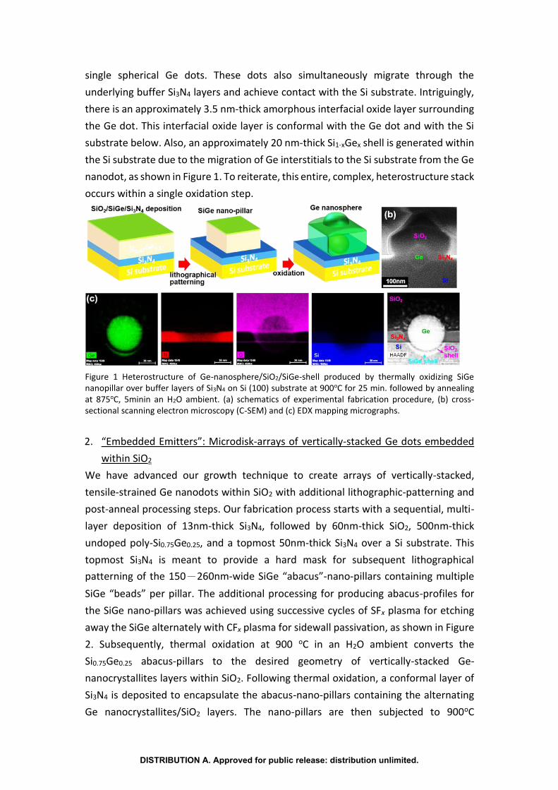
single spherical Ge dots. These dots also simultaneously migrate through the
underlying buffer Si3N4 layers and achieve contact with the Si substrate. Intriguingly,
there is an approximately 3.5 nm-thick amorphous interfacial oxide layer surrounding
the Ge dot. This interfacial oxide layer is conformal with the Ge dot and with the Si
substrate below. Also, an approximately 20 nm-thick Si1-xGex shell is generated within
the Si substrate due to the migration of Ge interstitials to the Si substrate from the Ge
nanodot, as shown in Figure 1. To reiterate, this entire, complex, heterostructure stack
occurs within a single oxidation step.
Figure 1 Heterostructure of Ge-nanosphere/SiO2/SiGe-shell produced by thermally oxidizing SiGe nanopillar over buffer layers of Si3N4 on Si (100) substrate at 900oC for 25 min. followed by annealing at 875oC, 5minin an H2O ambient. (a) schematics of experimental fabrication procedure, (b) cross-sectional scanning electron microscopy (C-SEM) and (c) EDX mapping micrographs.
2. “Embedded Emitters”: Microdisk-arrays of vertically-stacked Ge dots embedded
within SiO2
We have advanced our growth technique to create arrays of vertically-stacked,
tensile-strained Ge nanodots within SiO2 with additional lithographic-patterning and
post-anneal processing steps. Our fabrication process starts with a sequential, multi-
layer deposition of 13nm-thick Si3N4, followed by 60nm-thick SiO2, 500nm-thick
undoped poly-Si0.75Ge0.25, and a topmost 50nm-thick Si3N4 over a Si substrate. This
topmost Si3N4 is meant to provide a hard mask for subsequent lithographical
patterning of the 150-260nm-wide SiGe “abacus”-nano-pillars containing multiple
SiGe “beads” per pillar. The additional processing for producing abacus-profiles for
the SiGe nano-pillars was achieved using successive cycles of SFx plasma for etching
away the SiGe alternately with CFx plasma for sidewall passivation, as shown in Figure
2. Subsequently, thermal oxidation at 900 oC in an H2O ambient converts the
Si0.75Ge0.25 abacus-pillars to the desired geometry of vertically-stacked Ge-
nanocrystallites layers within SiO2. Following thermal oxidation, a conformal layer of
Si3N4 is deposited to encapsulate the abacus-nano-pillars containing the alternating
Ge nanocrystallites/SiO2 layers. The nano-pillars are then subjected to 900oC
DISTRIBUTION A. Approved for public release: distribution unlimited.

annealing in an O2 ambient to facilitate Ostwald-Ripening (coarsening) of the originally
small and irregularly-shaped Ge nanocrystallites into large, full-coalesced Ge
nanodots. Finally, we lithographically fabricated microdisks, each containing an array
of several nano-pillars with vertically-stacked, tens of nanometer-sized Ge nanodots
embedded within SiO2 matrices. The average diameter of these microdisks is 20m.
Figure 2 CSEM and CTEM micrographs of Si0.75Ge0.25 abacus-nanopillars, Ge-nanodot pillars, and microdisk pillar arrays. (a) Fabrication schematics and CSEM micrograph of the ultimate microdisk arrays of Ge nanodots. (b) Si0.75Ge0.25 abacus nanopillars lithographically formed by SF6/C4F8 plasma etching, (c) as-formed clusters of small, irregularly-shaped Ge nanocrystallites within SiO2 nanopillars following thermal oxidation of Si0.75Ge0.25 abacus-nanopillars, (d) Ostwald-ripening of Ge nanodots is facilitated by Si3N4 encapsulation and post annealing, (e) HRTEM of a single Ge nanodot, (f) XRD spectrum showing the high degree of crystallinity within the Ge nanodots. The presence of Al signals could be due to the background signals from the sample holder, since Al signals were also observed for the controlled sample of Si substrate.
3. Ge-dot PhotoMOSFETs fabrication.
The fabrication of Ge-dot PTs was initiated using n-Si(100) substrates with resistivity
between 0.090.7 Ωcm. Following local oxidation isolation processes, BF2 (1×10¹⁵
cm−2, 40 keV) and phosphorus (1×1015 cm−2, 30 keV) dopants were implanted for the
formation of source/drain and substrate electrodes, respectively, for p-channel PTs.
Next, a tri-layer deposition was conducted using sequential low-pressure chemical
vapor deposition of 35nm-thick Si3N4, followed by 70 nm-thick poly-Si0.85Ge0.15, and
finally a capping layer of 5 nm-thick SiO2. The topmost SiO2 layer is deposited for acting
as a hard mask for the subsequent plasma etching to define SiGe nanopillars. The
buffer Si3N4 layer between the Si0.85Ge0.15 nanopillars and the Si substrate serves as
the initial, local source of Si interstitials for promoting the coalescence and migration
DISTRIBUTION A. Approved for public release: distribution unlimited.
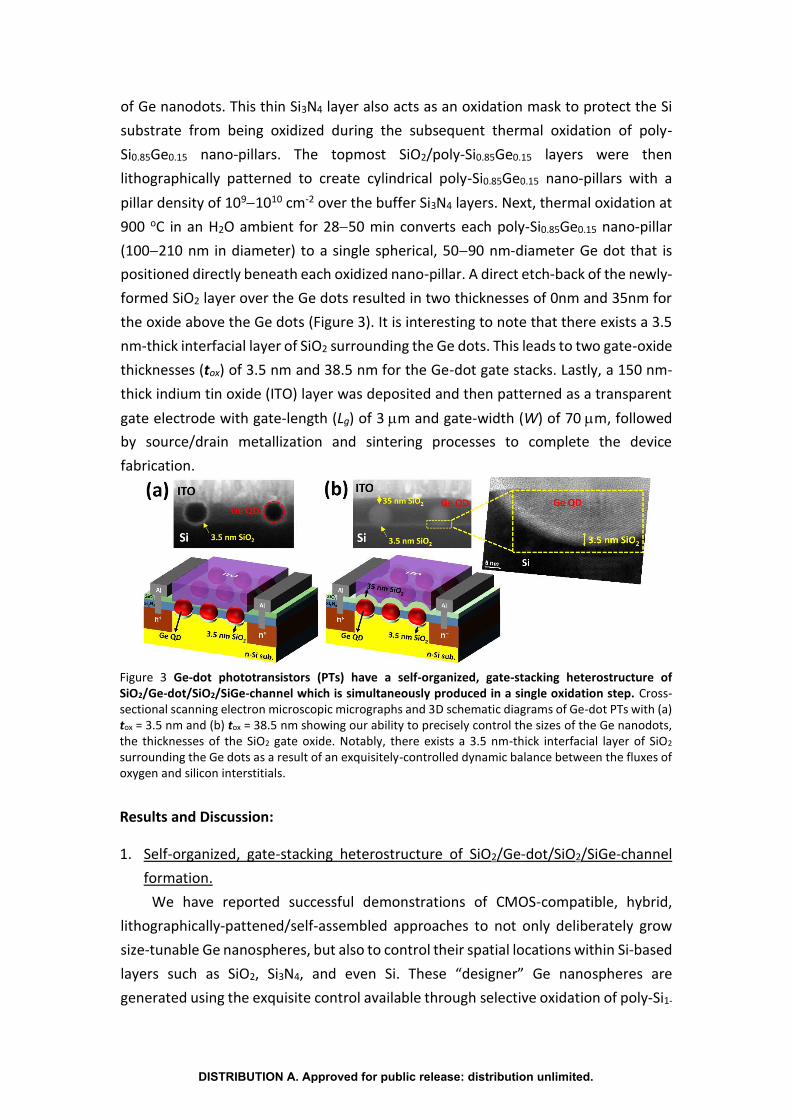
of Ge nanodots. This thin Si3N4 layer also acts as an oxidation mask to protect the Si
substrate from being oxidized during the subsequent thermal oxidation of poly-
Si0.85Ge0.15 nano-pillars. The topmost SiO2/poly-Si0.85Ge0.15 layers were then
lithographically patterned to create cylindrical poly-Si0.85Ge0.15 nano-pillars with a
pillar density of 1091010 cm-2 over the buffer Si3N4 layers. Next, thermal oxidation at
900 oC in an H2O ambient for 2850 min converts each poly-Si0.85Ge0.15 nano-pillar
(100210 nm in diameter) to a single spherical, 5090 nm-diameter Ge dot that is
positioned directly beneath each oxidized nano-pillar. A direct etch-back of the newly-
formed SiO2 layer over the Ge dots resulted in two thicknesses of 0nm and 35nm for
the oxide above the Ge dots (Figure 3). It is interesting to note that there exists a 3.5
nm-thick interfacial layer of SiO2 surrounding the Ge dots. This leads to two gate-oxide
thicknesses (tox) of 3.5 nm and 38.5 nm for the Ge-dot gate stacks. Lastly, a 150 nm-
thick indium tin oxide (ITO) layer was deposited and then patterned as a transparent
gate electrode with gate-length (Lg) of 3m and gate-width (W) of 70m, followed
by source/drain metallization and sintering processes to complete the device
fabrication.
Figure 3 Ge-dot phototransistors (PTs) have a self-organized, gate-stacking heterostructure of SiO2/Ge-dot/SiO2/SiGe-channel which is simultaneously produced in a single oxidation step. Cross-sectional scanning electron microscopic micrographs and 3D schematic diagrams of Ge-dot PTs with (a) tox = 3.5 nm and (b) tox = 38.5 nm showing our ability to precisely control the sizes of the Ge nanodots, the thicknesses of the SiO2 gate oxide. Notably, there exists a 3.5 nm-thick interfacial layer of SiO2 surrounding the Ge dots as a result of an exquisitely-controlled dynamic balance between the fluxes of oxygen and silicon interstitials.
Results and Discussion:
1. Self-organized, gate-stacking heterostructure of SiO2/Ge-dot/SiO2/SiGe-channel
formation.
We have reported successful demonstrations of CMOS-compatible, hybrid,
lithographically-pattened/self-assembled approaches to not only deliberately grow
size-tunable Ge nanospheres, but also to control their spatial locations within Si-based
layers such as SiO2, Si3N4, and even Si. These “designer” Ge nanospheres are
generated using the exquisite control available through selective oxidation of poly-Si1-
DISTRIBUTION A. Approved for public release: distribution unlimited.
xGex nanopatterned-pillars grown over buffer layers of Si3N4 on Si substrates. During
the high-temperature oxidation of the Si1-xGex nano-pillars, the Si content of the Si1-
xGex nano-pillar is preferentially oxidized forming SiO2. The remaining Ge is squeezed
radially inwards to the core of the oxidized nano-pillar forming a cluster of irregularly-
shaped Ge nanocrystallites. An intriguing discovery is that for a given Ge content
within the Si1-xGex nano-pillars that sit directly over buffer Si3N4 layers, further high-
temperature thermal oxidation results in the “migration” and consolidation of the
segregated, irregularly-shaped Ge nanocrystallites within each pillar into fully-
coalesced, “spherical” Ge nanodots (Figure 1). These Ge nanospheres exhibit
controllable migration through the underlying buffer Si3N4 layer. We believe this is
because the Si3N4 layer acts as an initial, local source of Si interstitials that are released
via a process of Ge-catalyzed, enhanced local oxidation of Si3N4. The emitted Si
interstitials aid in both the migration and coarsening of these Ge nanocrystallites
through Ostwald Ripening. The coalescing Ge nanocrystallites, in turn, further
increase the generation of Si interstitials through the increased interfacial area for the
catalytic decomposition of the Si3N4 layers. The surfaces of the growing Ge
nanocrystallites act as “sinks” for these Si interstitials. Because of their affinity for Ge,
the released Si interstitials migrate to the surface of the Ge nanocrystallites. Here, the
Si facilitates the decomposition of surrounding oxide via the reaction: Si(interstitial) +
SiO2(s) 2SiO(g). Oxide decomposition creates voids in front of the Ge nanocrystallite
cluster promoting both Ostwald Ripening and the physical migration of the cluster or
fully-coalesced Ge nanodot forward to the source of Si interstitials. Additionally, the
oxygen interstitial concentration gradient (highest oxygen interstitial concentration at
the oxide top surface) causes the Si interstitials and SiO to consequently migrate in
the opposite direction to the Ge nanocrystallites, i.e. towards the source of higher
oxygen interstitial concentration. The Si atoms and SiO are subsequently oxidized at
the distal surface in the wake of the migrating Ge nanocrystallite, essentially
backfilling SiO2 behind the nanocrystallite, and thus further driving the downward
migration of the nanocrystallite. It is a known fact that there is a 2.25x volume
expansion when Si is converted to SiO2. The regenerated SiO2 layer expanding behind
the Ge nanocrystallite and the voids created ahead of the nanocrystallite therefore
propel the Ge nanocrystallite to migrate towards the source of the Si interstitials,
namely the Si3N4 layers. Thus, these unique migration and Ostwald Ripening behaviors
of the Ge nanodots are made possible by the “symbiotic” cooperation of Si, Ge and O
interstitials resulting in a unique SiO2 “Destruction-Construction” mechanism that
promotes both the migration and the Ostwald Ripening.
2. “Embedded Emitters”: Microdisk-arrays of vertically-stacked Ge dots embedded
within SiO2
DISTRIBUTION A. Approved for public release: distribution unlimited.
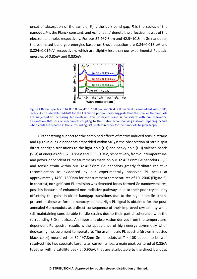
HRTEM, x-ray diffraction (XRD), Raman, and PL spectroscopies were employed to
examine the structural and optical properties of the Ge nanodots embedded within
the SiO2 layers. Figure 2(b-e) shows the results of cross-sectional scanning electron
microscopy (CSEM) and cross-sectional transmission electron microscopy (CTEM) of
the vertically-stacked Ge-nanodot array. It is seen that the consecutive
etching/protection processes using SF6 and C4F8 plasma respectively produces the
resulting Si0.75Ge0.25 abacus-nano-pillars with three sets of beads (Ge nanocrystallite
clusters) per pillar (Figure 2(b)). Thermal oxidation converts the SiGe abacus-pillars to
have vertically-stacked clusters of 8-10nm Ge nanocrystallites embedded within
oxide layers (Figure 2(c)). The subsequent encapsulation of the oxidized pillars by Si3N4
layers followed by post-annealing facilitates the consolidation of Ge nanocrystallites
via an Ostwald-Ripening process in which the large nanocrystallites grow at the
expense of small ones. Accompanying the completion of Ge nanocrystallite
coalescence to form large Ge nanodots is the remarkable change in the morphology
from irregular shapes to spherical shapes (Figure 2(d)). Most importantly, the
crystallinity of the Ge nanodots is significantly improved during the Ostwald-Ripening
process, as evidenced by the clear lattice fringes from HRTEM observations (Figure
2(e)) and by the diffraction peaks at 27.3o and 45.3o corresponding to Ge (111) and Ge
(220), respectively, from XRD examination (Figure 2(f)).
Further experimental support for the high-quality crystallinity of the Ge nanodots
embedded within the oxidized abacus-pillars is the appearance of strong longitudinal
optical (LO) Ge-Ge phonon lines ranging from 299.75cm−1288.67cm−1 measured for
Ge nanodots with corresponding sizes ranging from 675.8nm-32.47.8nm (Figure
4), which is in a sharp contrast to the observation of no measurable Raman line from
the as-grown, 810nm Ge nanocrystallites. The absence of GeO2 and Si/Ge
intermixing signals with predicted spectral-shifts of 440cm-1 and 400-410cm-1,
respectively, is indicative of the chemical purity of the Ge nanodots embedded within
the SiO2 matrices. Also previous, extensive TEM-based x-ray Fluorescence
measurements have confirmed that the nanodots are very nearly 100% Ge. In
comparison to the Raman line of 301.5cm−1 measured for bulk Ge, significant red-
shifts () of 1.75cm−1, 5.8cm−1, and 12.83cm−1 are observed for LO phonon lines
arising from 67.05.8nm, 42.510.8nm, and 32.47.8nm-sized Ge dots, respectively.
This suggests that the smaller Ge nanodots are subjected to increasing tensile-strain.
We show that not only matrix-induced strain but also QCE do indeed modify the
optical properties of our Ge nanodots embedded within SiO2, as evidenced by their
size-dependent PL wavelength measured for 32.47.8nm and for 42.510.8nm Ge
nanodots respectively (Figure 3(a)). An analytical equation reported by Brus et al.,
predicting the QCE in nanodots, is given by 𝐸 = 𝐸𝑔 + ℎ2
8𝑅2[
1
𝑚𝑒∗ +
1
𝑚ℎ∗ ], where E is the
DISTRIBUTION A. Approved for public release: distribution unlimited.
onset of absorption of the sample, Eg is the bulk band gap, R is the radius of the
nanodot, h is the Planck constant, and me* and mh
* denote the effective masses of the
electron and hole, respectively. For our 32.47.8nm and 42.510.8nm Ge nanodots,
the estimated band-gap energies based on Brus’s equation are 0.840.018 eV and
0.8240.014eV, respectively, which are slightly less than our experimental PL peak-
energies of 0.85eV and 0.835eV.
Figure 4 Raman spectra of 67.05.8 nm, 42.510.8 nm, and 32.47.8 nm Ge dots embedded within SiO2 layers. A considerable redshift for the LO Ge-Ge phonon peak suggests that the smaller Ge nanodots are subjected to increasing tensile-strain. This observed result is consistent with our theoretical explanation that loss of mechanical coupling to the matrix accompanying Ostwald Ripening occurs when voids are created in the surrounding SiO2 matrix in order for the nanodots to grow larger.
Further strong support for the combined effects of matrix-induced tensile-strains
and QCEs in our Ge nanodots embedded within SiO2 is the observation of strain-split
direct bandgap transitions to the light-hole (LH) and heavy-hole (HH) valence bands
(VBs) at energies of 0.820.85eV and 0.860.9eV, respectively, from our temperature-
and power-dependent PL measurements made on our 32.47.8nm Ge nanodots. QCE
and tensile-strain within our 32.47.8nm Ge nanodots greatly facilitate radiative
recombination as evidenced by our experimentally observed PL peaks at
approximately 14501500nm for measurement temperatures of 10200K (Figure 5).
In contrast, no significant PL emission was detected for as-formed Ge nanocrystallites,
possibly because of enhanced non-radiative pathways due to their poor crystallinity
offsetting the gains in direct bandgap transitions due to the higher tensile strains
present in these as-formed nanocrystallites. High PL signal is obtained for the post-
annealed Ge nanodots as a direct consequence of their improved crystallinity while
still maintaining considerable tensile-strains due to their partial coherence with the
surrounding SiO2 matrices. An important observation derived from the temperature-
dependent PL spectral results is the appearance of high-energy asymmetry when
decreasing measurement temperature. The asymmetric PL spectra (drawn in dotted
black color) measured for 32.47.8nm Ge nanodots at T = 10K appear to be well
resolved into two separate Lorentzian curve-fits, i.e., a main peak centered at 0.85eV
together with a satellite peak at 0.90eV, that are attributable to the direct bandgap
250 300 350 400 450 500 550
301 cm-1
Bulk Ge
Ge QD = 32 7.8 nm
Ra
ma
n i
nte
ns
ity
(a
rb.
un
its
)
Wave number (cm-1)
SiGe LO
Ge QD = 42 10.8 nm
Ge QD = 67 5.8 nm
±
±
±
DISTRIBUTION A. Approved for public release: distribution unlimited.
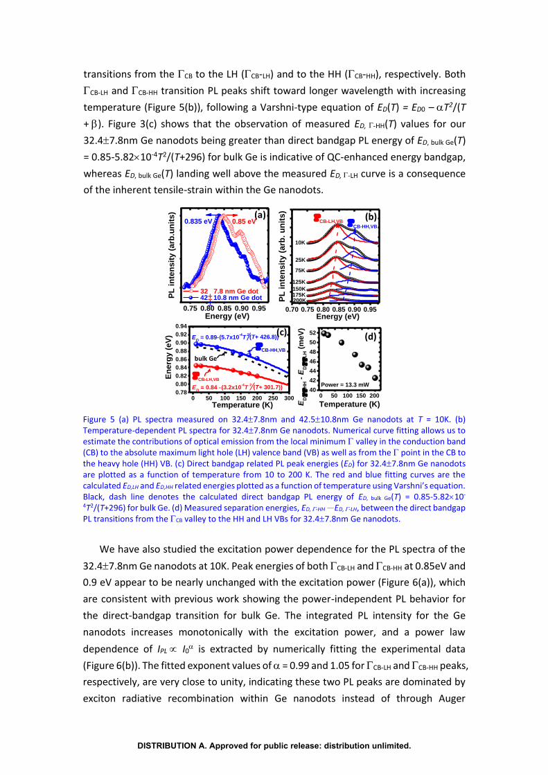
transitions from the CB to the LH (CB-LH) and to the HH (CB-HH), respectively. Both
CB-LH and CB-HH transition PL peaks shift toward longer wavelength with increasing
temperature (Figure 5(b)), following a Varshni-type equation of ED(T) = ED0 –T2/(T
+). Figure 3(c) shows that the observation of measured ED, -HH(T) values for our
32.47.8nm Ge nanodots being greater than direct bandgap PL energy of ED, bulk Ge(T)
= 0.85-5.8210-4T2/(T+296) for bulk Ge is indicative of QC-enhanced energy bandgap,
whereas ED, bulk Ge(T) landing well above the measured ED, -LH curve is a consequence
of the inherent tensile-strain within the Ge nanodots.
Figure 5 (a) PL spectra measured on 32.47.8nm and 42.510.8nm Ge nanodots at T = 10K. (b) Temperature-dependent PL spectra for 32.47.8nm Ge nanodots. Numerical curve fitting allows us to estimate the contributions of optical emission from the local minimum valley in the conduction band (CB) to the absolute maximum light hole (LH) valence band (VB) as well as from the point in the CB to the heavy hole (HH) VB. (c) Direct bandgap related PL peak energies (ED) for 32.47.8nm Ge nanodots are plotted as a function of temperature from 10 to 200 K. The red and blue fitting curves are the calculated ED,LH and ED,HH related energies plotted as a function of temperature using Varshni’s equation. Black, dash line denotes the calculated direct bandgap PL energy of ED, bulk Ge(T) = 0.85-5.8210-
4T2/(T+296) for bulk Ge. (d) Measured separation energies, ED, -HH-ED, -LH, between the direct bandgap PL transitions from the CB valley to the HH and LH VBs for 32.47.8nm Ge nanodots.
We have also studied the excitation power dependence for the PL spectra of the
32.47.8nm Ge nanodots at 10K. Peak energies of both CB-LH and CB-HH at 0.85eV and
0.9 eV appear to be nearly unchanged with the excitation power (Figure 6(a)), which
are consistent with previous work showing the power-independent PL behavior for
the direct-bandgap transition for bulk Ge. The integrated PL intensity for the Ge
nanodots increases monotonically with the excitation power, and a power law
dependence of IPL I0 is extracted by numerically fitting the experimental data
(Figure 6(b)). The fitted exponent values of = 0.99 and 1.05 for CB-LH and CB-HH peaks,
respectively, are very close to unity, indicating these two PL peaks are dominated by
exciton radiative recombination within Ge nanodots instead of through Auger
0.70 0.75 0.80 0.85 0.90 0.95
PL
in
ten
sit
y (
arb
. u
nit
s)
Energy (eV)
CB-LH,VB
CB-HH,VB
10K
25K
75K
125K
150K175K200K
0 50 100 150 20040
42
44
46
48
50
52
Power = 13.3 mW
ED
,-
HH -
ED
,-
LH (
me
V)
Temperature (K)
0.75 0.80 0.85 0.90 0.95
32 7.8 nm Ge dot
0.85 eV0.835 eV
PL
in
ten
sit
y (
arb
.un
its)
Energy (eV)
42 10.8 nm Ge dot±±
(a) (b)
(d)
0 50 100 150 200 250 3000.78
0.80
0.82
0.84
0.86
0.88
0.90
0.92
0.94
En
erg
y (
eV
)
Temperature (K)
CB-HH,VB
(5.7x10⁻⁴T
2 E
D = 0.89- (T+ 426.8))
CB-LH,VB
ED = 0.84 - (3.2x10
-4T
2(T+ 301.7))
(c)
bulk Ge
DISTRIBUTION A. Approved for public release: distribution unlimited.
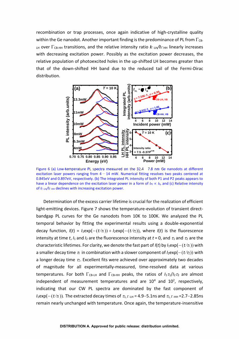
recombination or trap processes, once again indicative of high-crystalline quality
within the Ge nanodot. Another important finding is the predominance of PL from CB-
LH over CB-HH transitions, and the relative intensity ratio I-LH/I-HH linearly increases
with decreasing excitation power. Possibly as the excitation power decreases, the
relative population of photoexcited holes in the up-shifted LH becomes greater than
that of the down-shifted HH band due to the reduced tail of the Fermi-Dirac
distribution.
Figure 6 (a) Low- e nanodots at different excitation laser powers ranging from 4-14 mW. Numerical fitting resolves two peaks centered at 0.845eV and 0.897eV, respectively. (b) The integrated PL intensity of both P1 and P2 peaks appears to have a linear dependence on the excitation laser power in a form of IPL I0, and (c) Relative intensity of I-LH/I-HH declines with increasing excitation power.
Determination of the excess carrier lifetime is crucial for the realization of efficient
light-emitting devices. Figure 7 shows the temperature-evolution of transient direct-
bandgap PL curves for the Ge nanodots from 10K to 100K. We analyzed the PL
temporal behavior by fitting the experimental results using a double-exponential
decay function, I(t) = I1exp(tI2exp(t, where I(t) is the fluorescence
intensity at time t, I1 and I2 are the fluorescence intensity at t = 0, and 1 and 2are the
characteristic lifetimes. For clarity, we denote the fast part of I(t) by I1exp(t with
a smaller decay time in combination with a slower component of I2exp(twith
a longer decay time . Excellent fits were achieved over approximately two decades
of magnitude for all experimentally-measured, time-resolved data at various
temperatures. For both CB-LH and CB-HH peaks, the ratios of I11/I22 are almost
independent of measurement temperatures and are 104 and 102, respectively,
indicating that our CW PL spectra are dominated by the fast component of
I1exp(tThe extracted decay times of 1, -LH = 4.95.1ns and 1, -HH =2.72.85ns
remain nearly unchanged with temperature. Once again, the temperature-insensitive
0.70 0.75 0.80 0.85 0.90 0.95
PL
in
ten
sit
y (
arb
.un
its
)
Energy (eV)
T = 10 K(a)
13.3mW
11mW
10mW
8mW
5.3mW
4mW
4 6 8 10 12 14
3
4
5
6
HH
PL
in
ten
sit
y
LH
PL
in
ten
sit
y
Power (mW)
= 7.5 -0.37P0.98
T = 10 K (c)
4 6 8 10 12 14
Inte
gra
ted
PL
CB-HH, VB
CB-LH, VB
inte
ns
ity
(arb
.un
its
)Incident power (mW)
IPL
= . Io (b)
Intensity ratio
DISTRIBUTION A. Approved for public release: distribution unlimited.
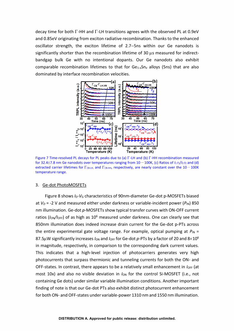
decay time for both -HH and -LH transitions agrees with the observed PL at 0.9eV
and 0.85eV originating from exciton radiative recombination. Thanks to the enhanced
oscillator strength, the exciton lifetime of 2.75ns within our Ge nanodots is
significantly shorter than the recombination lifetime of 30s measured for indirect-
bandgap bulk Ge with no intentional dopants. Our Ge nanodots also exhibit
comparable recombination lifetimes to that for Ge1-xSnx alloys (5ns) that are also
dominated by interface recombination velocities.
Figure 7 Time-resolved PL decays for PL peaks due to (a) -LH and (b) -HH recombination measured for 32.47.8 nm Ge nanodots over temperatures ranging from 10-100K, (c) Ratios of I11/I22 and (d) extracted carrier lifetimes forCB-LH, and CB-HH, respectively, are nearly constant over the 10-100K temperature range.
3. Ge-dot PhotoMOSFETs
Figure 8 shows ID-VG characteristics of 90nm-diameter Ge-dot p-MOSFETs biased
at VD = -2 V and measured either under darkness or variable-incident power (PIN) 850
nm illumination. Ge-dot p-MOSFETs show typical transfer curves with ON-OFF current
ratios (ION/IOFF) of as high as 106 measured under darkness. One can clearly see that
850nm illumination does indeed increase drain current for the Ge-dot p-PTs across
the entire experimental gate voltage range. For example, optical pumping at PIN =
87.5W significantly increases ION and IOFF for Ge-dot p-PTs by a factor of 20 and 8106
in magnitude, respectively, in comparison to the corresponding dark current values.
This indicates that a high-level injection of photocarriers generates very high
photocurrents that surpass thermionic and tunneling currents for both the ON- and
OFF-states. In contrast, there appears to be a relatively small enhancement in IOFF (at
most 10x) and also no visible deviation in ION for the control Si-MOSFET (i.e., not
containing Ge dots) under similar variable illumination conditions. Another important
finding of note is that our Ge-dot PTs also exhibit distinct photocurrent enhancement
for both ON- and OFF-states under variable-power 1310 nm and 1550 nm illumination.
DISTRIBUTION A. Approved for public release: distribution unlimited.
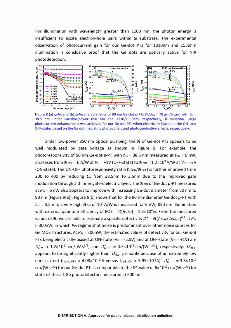
For illumination with wavelength greater than 1100 nm, the photon energy is
insufficient to excite electron-hole pairs within Si substrate. The experimental
observation of photocurrent gain for our Ge-dot PTs for 1310nm and 1550nm
illumination is conclusive proof that the Ge dots are optically active for NIR
photodetection.
Figure 8 (a) ID-VG and (b) ID-VD characteristics of 90 nm Ge-dot p-PTs (Wg/Lg = 70m/3m) with tox = 38.5 nm under variable-power 850 nm and 1310/1550nm, respectively, illumination. Large photocurrent enhancement was achieved for our Ge-dot PTs when electrically-biased in the ON- and OFF-states based on the Ge dot mediating photovoltaic and photoconductive effects, respectively.
Under low-power 850 nm optical pumping, the of Ge-dot PTs appears to be
well modulated by gate voltage as shown in Figure 9. For example, the
photoresponsivity of 50 nm Ge-dot p-PT with tox = 38.5 nm measured at PIN = 6 nW,
increases from OFF = 6 A/W at VG = +1V (OFF-state) to ON = 1.2103 A/W at VG = -2V
(ON-state). The ON-OFF photoresponsivity ratio (ON/OFF) is further improved from
200 to 400 by reducing tox from 38.5nm to 3.5nm due to the improved gate
modulation through a thinner gate-dielectric layer. The ON of Ge-dot p-PT measured
at PIN = 6 nW also appears to improve with increasing Ge-dot diameter from 50 nm to
90 nm (Figure 9(a)). Figure 9(b) shows that for the 90 nm-diameter Ge-dot p-PT with
tox = 3.5 nm, a very high ON of 104 A/W is measured for 6 nW, 850 nm illumination
with external quantum efficiency of EQE =[h/e] = 1.5106%. From the measured
values of , we are able to estimate a specific detectivity D* =(AGate/2eIdark)0.5at PIN
> 300nW, in which PIN regime shot noise is predominant over other noise sources for
Ge MOS structures. At PIN = 300nW, the estimated values of detectivity for our Ge-dot
PTs being electrically-biased at ON-state (VG = -2.5V) and at OFF-state (VG = +1V) are
𝐷𝑂𝑁∗ 1.21011 cm/(Ws1/2) and 𝐷𝑂𝐹𝐹
∗ 3.51012 cm/(Ws1/2), respectively. 𝐷𝑂𝐹𝐹∗
appears to be significantly higher than 𝐷𝑂𝑁∗ primarily because of an extremely low
dark current (Idark, OFF 4.0810-11A versus Idark, ON 5.9510-5A). 𝐷𝑂𝐹𝐹∗ 3.51012
cm/(Ws1/2) for our Ge-dot PTs is comparable to the D* value of 61012 cm/(Ws1/2) for
state-of-the-art Ge photodetectors measured at 600 nm.
DISTRIBUTION A. Approved for public release: distribution unlimited.
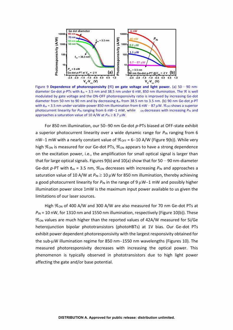
Figure 9 Dependence of photoresponsivity () on gate voltage and light power. (a) 50-90 nm-diameter Ge-dot p-PTs with tox = 3.5 nm and 38.5 nm under 6 nW, 850 nm illumination. The is well modulated by gate voltage and the ON-OFF photoresponsivity ratio is improved by increasing Ge-dot diameter from 50 nm to 90 nm and by decreasing tox from 38.5 nm to 3.5 nm. (b) 90 nm Ge-dot p-PT with tox = 3.5 nm under variable-power 850 nm illumination from 6 nW-87 W. OFF shows a superior photocurrent linearity for PIN ranging from 6 nW ON decreases with increasing PIN and approaches a saturation value of 10 A/W at PIN 8.7W.
For 850 nm illumination, our 5090 nm Ge-dot p-PTs biased at OFF-state exhibit
a superior photocurrent linearity over a wide dynamic range for PIN ranging from 6
nW1 mW with a nearly constant value ofOFF = 610 A/W (Figure 9(b)). While very
high ON is measured for our Ge-dot PTs, ON appears to have a strong dependence
on the excitation power, i.e., the amplification for small optical signal is larger than
that for large optical signals. Figures 9(b) and 10(a) show that for 50-90 nm-diameter
Ge-dot p-PT with tox = 3.5 nm, ON decreases with increasing PIN and approaches a
saturation value of 10 A/W at PIN 10 W for 850 nm illumination, thereby achieving
a good photocurrent linearity for PIN in the range of 9 W1 mW and possibly higher
illumination power since 1mW is the maximum input power available to us given the
limitations of our laser sources.
High ON of 400 A/W and 300 A/W are also measured for 70 nm Ge-dot PTs at
PIN = 10 nW, for 1310 nm and 1550 nm illumination, respectively (Figure 10(b)). These
ON values are much higher than the reported values of 42A/W measured for Si/Ge
heterojunction bipolar phototransistors (photoHBTs) at 1V bias. Our Ge-dot PTs
exhibit power dependent photoresponsivity with the largest responsivity obtained for
the sub-W illumination regime for 850 nm1550 nm wavelengths (Figures 10). The
measured photoresponsivity decreases with increasing the optical power. This
phenomenon is typically observed in phototransistors due to high light power
affecting the gate and/or base potential.
DISTRIBUTION A. Approved for public release: distribution unlimited.
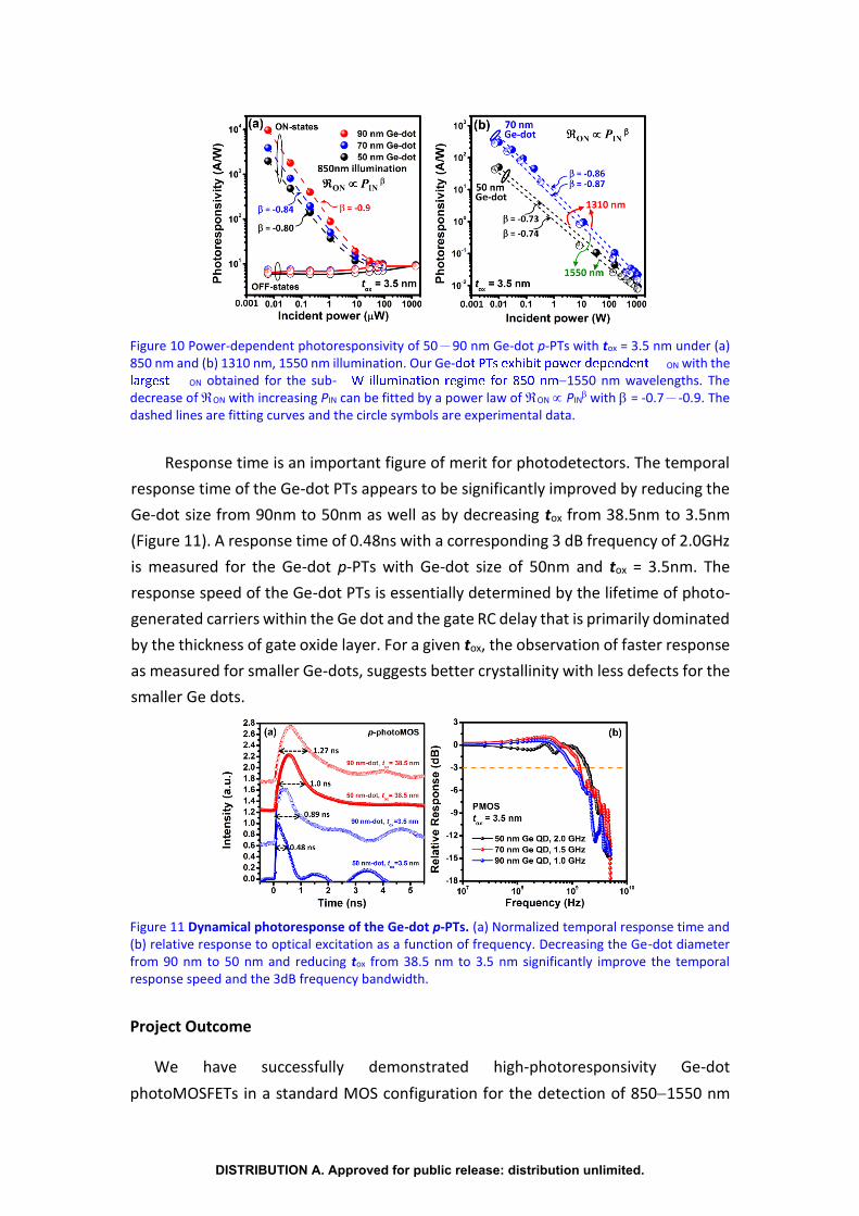
Figure 10 Power-dependent photoresponsivity of 50-90 nm Ge-dot p-PTs with tox = 3.5 nm under (a) 850 nm and (b) 1310 nm, 1550 nm illumination. Our Ge- ON with the
ON obtained for the sub- 1550 nm wavelengths. The decrease of ON with increasing PIN can be fitted by a power law of ON PIN
with = -0.7--0.9. The dashed lines are fitting curves and the circle symbols are experimental data.
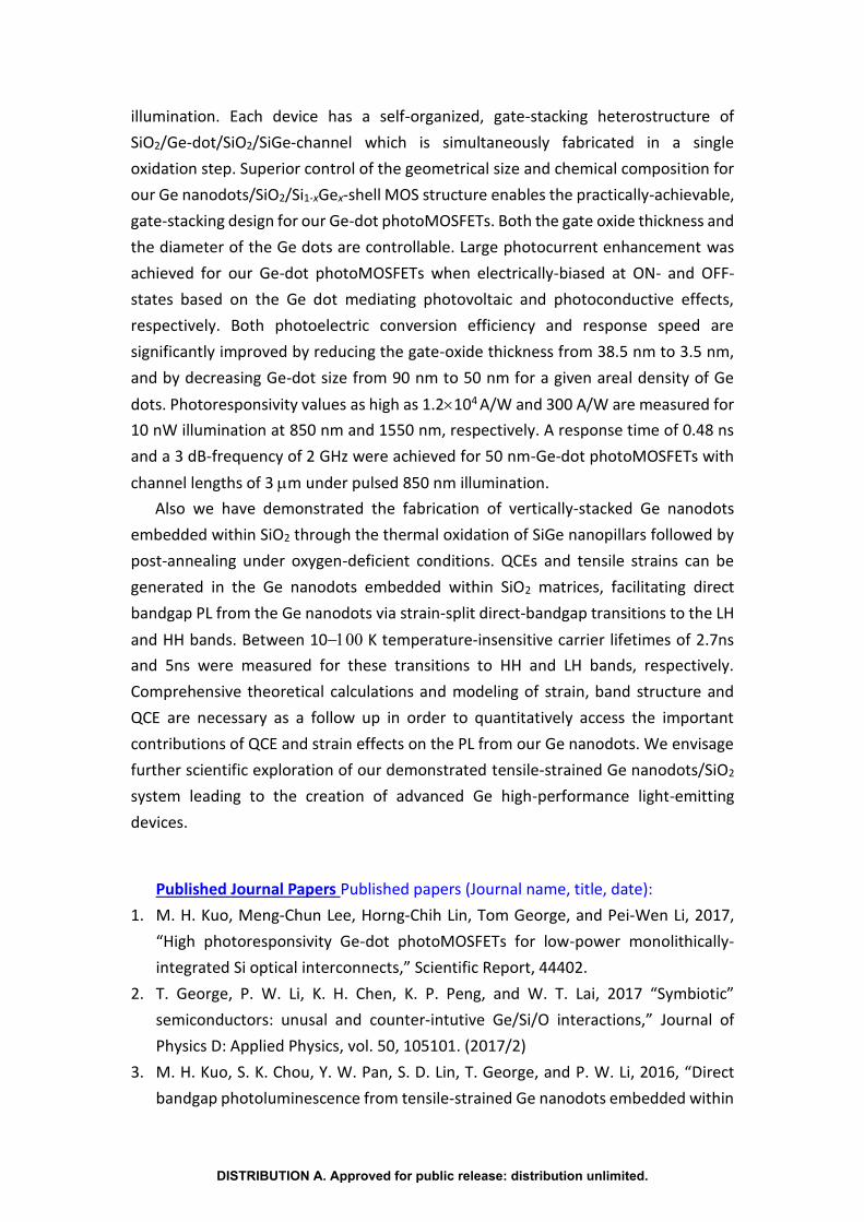
Response time is an important figure of merit for photodetectors. The temporal
response time of the Ge-dot PTs appears to be significantly improved by reducing the
Ge-dot size from 90nm to 50nm as well as by decreasing tox from 38.5nm to 3.5nm
(Figure 11). A response time of 0.48ns with a corresponding 3 dB frequency of 2.0GHz
is measured for the Ge-dot p-PTs with Ge-dot size of 50nm and tox = 3.5nm. The
response speed of the Ge-dot PTs is essentially determined by the lifetime of photo-
generated carriers within the Ge dot and the gate RC delay that is primarily dominated
by the thickness of gate oxide layer. For a given tox, the observation of faster response
as measured for smaller Ge-dots, suggests better crystallinity with less defects for the
smaller Ge dots.
Figure 11 Dynamical photoresponse of the Ge-dot p-PTs. (a) Normalized temporal response time and (b) relative response to optical excitation as a function of frequency. Decreasing the Ge-dot diameter from 90 nm to 50 nm and reducing tox from 38.5 nm to 3.5 nm significantly improve the temporal response speed and the 3dB frequency bandwidth.
Project Outcome
We have successfully demonstrated high-photoresponsivity Ge-dot
photoMOSFETs in a standard MOS configuration for the detection of 8501550 nm
DISTRIBUTION A. Approved for public release: distribution unlimited.
illumination. Each device has a self-organized, gate-stacking heterostructure of
SiO2/Ge-dot/SiO2/SiGe-channel which is simultaneously fabricated in a single
oxidation step. Superior control of the geometrical size and chemical composition for
our Ge nanodots/SiO2/Si1-xGex-shell MOS structure enables the practically-achievable,
gate-stacking design for our Ge-dot photoMOSFETs. Both the gate oxide thickness and
the diameter of the Ge dots are controllable. Large photocurrent enhancement was
achieved for our Ge-dot photoMOSFETs when electrically-biased at ON- and OFF-
states based on the Ge dot mediating photovoltaic and photoconductive effects,
respectively. Both photoelectric conversion efficiency and response speed are
significantly improved by reducing the gate-oxide thickness from 38.5 nm to 3.5 nm,
and by decreasing Ge-dot size from 90 nm to 50 nm for a given areal density of Ge
dots. Photoresponsivity values as high as 1.2104 A/W and 300 A/W are measured for
10 nW illumination at 850 nm and 1550 nm, respectively. A response time of 0.48 ns
and a 3 dB-frequency of 2 GHz were achieved for 50 nm-Ge-dot photoMOSFETs with
channel lengths of 3 m under pulsed 850 nm illumination.
Also we have demonstrated the fabrication of vertically-stacked Ge nanodots
embedded within SiO2 through the thermal oxidation of SiGe nanopillars followed by
post-annealing under oxygen-deficient conditions. QCEs and tensile strains can be
generated in the Ge nanodots embedded within SiO2 matrices, facilitating direct
bandgap PL from the Ge nanodots via strain-split direct-bandgap transitions to the LH
and HH bands. Between 10K temperature-insensitive carrier lifetimes of 2.7ns
and 5ns were measured for these transitions to HH and LH bands, respectively.
Comprehensive theoretical calculations and modeling of strain, band structure and
QCE are necessary as a follow up in order to quantitatively access the important
contributions of QCE and strain effects on the PL from our Ge nanodots. We envisage
further scientific exploration of our demonstrated tensile-strained Ge nanodots/SiO2
system leading to the creation of advanced Ge high-performance light-emitting
devices.
Published Journal Papers Published papers (Journal name, title, date):
1. M. H. Kuo, Meng-Chun Lee, Horng-Chih Lin, Tom George, and Pei-Wen Li, 2017,
“High photoresponsivity Ge-dot photoMOSFETs for low-power monolithically-
integrated Si optical interconnects,” Scientific Report, 44402.
2. T. George, P. W. Li, K. H. Chen, K. P. Peng, and W. T. Lai, 2017 “Symbiotic”
semiconductors: unusal and counter-intutive Ge/Si/O interactions,” Journal of
Physics D: Applied Physics, vol. 50, 105101. (2017/2)
3. M. H. Kuo, S. K. Chou, Y. W. Pan, S. D. Lin, T. George, and P. W. Li, 2016, “Direct
bandgap photoluminescence from tensile-strained Ge nanodots embedded within
DISTRIBUTION A. Approved for public release: distribution unlimited.
SiO2,” J. Appl. Phys., vol. 120, 233106 (2016)
4. Ching-Chi Wang, Wei-Ting Lai, Yi-Yeh Hsiao, Inn-Hao Chen, Tom George, Pei-Wen
Li, 2016, “Geometry-dependent phase, stress state and electrical properties in
nickel-silicide nanowires," Journal of Physics D: Applied Physics, vol. 49, 204102.
(2016/4)
5. Chin-I Kuan, Horng-Chih Lin, Pei-Wen Li, and Tiao-Yuan Huang, 2016 “High-
performance submicron ZnON thin-Film transistors with supreme field-effect
mobility,” IEEE Electron Device Lett., vol. 37, no. 3, 303.
6. Wei-Ting Lai, Kuo-Ching Yang, Po-Hsiang Liao, Tom George, and Pei-Wen Li, 2016,
“Gate-stack engineering for self-aligned Ge-dot/SiO2/SiGe-shell MOS capacitors,”
Frontiers in Materials, vol. 3, 00005.
7. Shuo-Huang Yuan, Zing-Way Pei, Pei-Wen Li, Yi-Jen Chan, 2015, “Au Nanoparticle
Light Scattering Enhanced Responsivity in Pentacene Phototransistor for Deep-UV
Light Detection,” IEEE Electron Device Letters, vol. 36, 1186. (2015/11)
8. S.H. Yuan, Z. Pei, H.C. Lai, P.W. Li, and Y.J. Chan, 2015, “Pentacene phototransistor
with gate voltage independent responsivity and sensitivity by small silver
nanoparticles decoration,” Organic Electronics, vol. 27, 711. (2015/8)
9. W. T. Lai, K. C. Yang, T. C. Hsu, P. H. Liao, T. George, and P. W. Li, 2015, “A Unique
Approach to Generate Self-Aligned SiO2/Ge/SiO2/SiGe Gate-Stacking
Heterostructures in a Single Fabrication Step,” Nanoscale Research Letters, vol. 10,
224. (2015/05)
10. M. H. Kuo, W. T. Lai, S. W. Lee, and P. W. Li, 2015, “Design of multifold Ge/Si/Ge
composite quantum-dot heterostructures for visible to near-infrared
photodetection, Optics Letters, vol. 40, 2401-2404. (2015/5)
11. K. H. Chen, C. C. Wang, W. T. Lai, T. George, and P. W. Li, 2015, “The Pivotal Role
of Oxygen Interstitials in the Dynamics of Growth and Movement of Germanium
Nanocrystallites,” CrystEngComm, vol. 17, 6370 – 6375.
Paper currently under review (journal name, title, date accepted):
(1) Andriy Nadtochiy, Vasyl Kuryliuk, Oleg Korotchenkov, Pei-Wen Li & Sheng-Wei
Lee, 2016, “Evidence for an enhanced thermoelectric performance of
composite Ge/Si quantum dots,”submitted Scientific Reports.
(2) Chin-I Kuan, Horng-Chih Lin, Pei-Wen Li, and Tiao-Yuan Huang, 2016,
“Performance Improvement of ZnO Thin-Film Transistors with ZnON
Source/Drain Contacts,”
(3) Ming-Hao Kuo, Ping-Che Liu, Po-Yu Hong, Meng-Chun Lee, Horng-Chih Lin, Tom
George, and Pei-Wen Li, 2017, “Very large photoresponsiviy and high
photocurrent linearity for Ge-dot/SiO2/SiGe photoMOSFETs under gate
DISTRIBUTION A. Approved for public release: distribution unlimited.
modulation”, submitted to APL Photonics.
12. Conference paper/poster/presentation (conf. name, title, date):
(1) M. H. Kuo, B. J. Liu, T. L. Huang, H. C. Lin, and P. W. Li, 2017, "Very large
photogain and high photorespone linearity of Ge-dot photoMOSFETs
operating in accumulation-mode for monolithic Si photonics,” 2017 Silicon
Nanoelectronics Workshop, Kyoto, June 4-6.
(2) C. Y. Hsueh, T. L. Huang, K. P. Peng, M. H. Kuo, H. C. Lin, and P. W. Li, "Counter-
intuitive Ge/Si/O interactions and Ge/Si symbiosis enable the creatation of
new classes of exciting nanoelectronic and nanophotonic devices" 2017
Silicon Nanoelectronics Workshop, Kyoto, June 4-6.
(3) Ming-Hao Kuo, M. C. Lee, J. W. Tien, Wei-Ting Lai, and Pei-Wen Li, “Optimal
design of Ge-dot photoMOSFETs for highly-integrated monolithic Si
Photonics”, presented in Optical Fiber Conference, Los Angel, USA (March 19-
23 2017)
(4) M. H. Kuo, Ming-Hao Kuo, Meng-Chun Lee, and Pei-Wen Li,, “High
Photoresponsivity Germanium Nanodot PhotoMOSFETs for Monolithically-
Integrated Si Optical Interconnects,” 1st Electron Devices Technology and
Manufacturing, Toyama, Japan (2017/2/28-3/2)
(5) C. W. Tien, P. H. Liao, K. P. Peng, H. C. Lin, and P. W. Li, “Channel engineering
of self-organized Ge-nanosphere/SiO2/Si1-xGex-channel heterostructure on Si
for Ge MOSFETs,” oral presentation in 2016 International Electron Device and
Material Symposium, Tainan, Taiwan.(2016/11/17-18)
(6) Po-Hsiang Liao, Shih-Cing Luo1, Kang-Ping Peng, Horng-Chih Lin, Tom George,
and Pei-Wen Li, “Controllability of gate-stacking heterostructure of Ge
gate/SiO2/SiGe channel fabricated by one-step high temperature oxidation
process”, oral presentation in 2016 International Electron Device and
Material Symposium, Tainan, Taiwan.(2016/11/17-18)
(7) Tom George, Pei-Wen Li, K. H. Chen, I. H. Chen, and W. T. Lai, “The
Germanium Surprise! Unusual and Counter-Intuitive Ge/Si/O Interactions
Result in Unique Nano-Optoelectronic Devices,” oral presentation in 2016
International Electron Device and Material Symposium, Tainan,
Taiwan.(2016/11/17-18).
(8) P. H. Liao, C. W. Tien, K. P. Peng, H. C. Lin, Tom George, and P. W. Li,, 2016,
“Gate-stack engineering of self-organized nanospherical Ge gate/SiO2/Si1-
xGex channel on Si (100) and Si (110) for Ge MOS devices,” International
Conference on Solid-State Devices and Materials, Sapporo, Japan (Sep. 25-30,
2016)
DISTRIBUTION A. Approved for public release: distribution unlimited.
(9) M. H. Kuo, S. K. Chou, W. T. Lai,Y. W. Pan, S. D. Lin, Tom George, and P. W. Li,
2016, “Experimental observation of direct bandgap photoluminescence from
tensile-strained Ge nanodots embedded within SiO2 matrix,” International
Conference on Solid-State Devices and Materials, Sapporo, Japan (Sep. 25-30,
2016)
(10) Ming-Hung Wu, Horng-Chih Lin, Pei-Wen Li, Tiao-Yuan Huang, 2016, “Film-
Profile-Engineered IGZO Thin-Film Transistors with Gate/Drain Offset for High
Voltage Operation,” 23rd IEEE International Symposium on the Physical and
Failure Analysis of Integrated Circuits (IPFA 2016), Singapore, 18-21 July 2016
(11) Horng-Chih Lin, Chin-I Kuan, Pei-Wen Li, and Tiao-Yuan Huang, “Short-
Channel ZnON Thin-Film Transistors with Film Profile Engineering,” 2016
Silicon Nanoelectronics Workshop, Honolulu, June 11-12.
(12) Horng-Chih Lin, Chen-Chen Yang, Yung-Chen Chen, Ruey Dar Chang, Pei-
Wen Li, and Tiao-Yuan Huang, “Fabrication and RTN Characteristics of Gate-
All-Around Poly-Si Junctionless Nanowire Transistors,” 2016 Silicon
Nanoelectronics Workshop, Honolulu, June 11-12.
(13) M. H. Kuo, M. C. Lee, C. W. Tien, W. T. Lai, and P. W. Li, “Optimal design of
Ge-dot photoMOSFETs for highly-integrated monolithic Si Photonics,” 2016
Silicon Nanoelectronics Workshop, Honolulu, June 11-12.
(14) P.W. Li (invited talk) 2016, “Designer Ge Quantum-Dot Phototransistors
for highly-integrated, broadband optical interconnects,”IEEE INEC, Chengdu,
China, May 9-11 2016.
(15) P. W. Li (invited talk) 2016, “Germanium quantum dots for functional
sensing devices,” CSWNST 2016, Taipei, Taiwan (2016/03/23-24).
(16) R. J. Lu, T. Y. Huang, P. W. Li, and H. C. Lin, 2016 "High-gain, Low-voltage
BEOL Logic Gate Inverter Built with Film Profile Engineered IGZO Transistors",
oral presentation in VLSI-TSA, Hsinchu, Taiwan, 25-287 April, 2016.
(17) Horng-Chih Lin, Chin-I Kuan, Pei-Wen Li, and Tiao-Yuan Huang, “Short-
Channel ZnON Thin-Film Transistors with Film Profile Engineering,” 2016
Silicon Nanoelectronics Workshop, Honolulu, June 11-12, 2016.
(18) Horng-Chih Lin, Chen-Chen Yang, Yung-Chen Chen, Ruey Dar Chang, Pei-
Wen Li, and Tiao-Yuan Huang, “Fabrication and RTN Characteristics of Gate-
All-Around Poly-Si Junctionless Nanowire Transistors,” 2016 Silicon
Nanoelectronics Workshop, Honolulu, June 11-12, 2016.
(19) M. H. Kuo, M. C. Lee, C. W. Tien, W. T. Lai, and P. W. Li, “Optimal design of
Ge-dot photoMOSFETs for highly-integrated monolithic Si Photonics,” 2016
Silicon Nanoelectronics Workshop, Honolulu, June 11-12.
(20) R. J. Lu, T. Y. Huang, P. W. Li, and H. C. Lin, 2016 "High-gain, Low-voltage
DISTRIBUTION A. Approved for public release: distribution unlimited.
BEOL Logic Gate Inverter Built with Film Profile Engineered IGZO Transistors",
oral presentation in VLSI-TSA, Hsinchu, Taiwan, 25-287 April, 2016.
(21) C. C. Wang, C. S. Jhou, C. L. Hsin, W. T. Lai, and P. W. Li, 2015, “Effects of
array size- and Ge-content on cooling efficiency of poly-Si1-xGex nanopillars
thermoelectric coolers,” oral presentation in 2015 International Electron
Device and Material Symposium, Tainan, Taiwan.(2015/11/1920)
(22) M. H. Kuo, S. K. Chou, W. T. Lai, Y. W. Pan, S. D. Lin, and P. W. Li, 2015,
“Direct Bandgap Photoluminescence from SiO2 Matrix Induced Tensile-
strained Ge Quantum Dots,” oral presentation in 2015 International Electron
Device and Material Symposium, Tainan, Taiwan. (2015/11/1920)
(23) M. H. Kuo, S. Y. Hong, P. C. Chen, W. T. Lai, M. C. Lee, and P. W. Li, 2015,
“Optimal Design and Fabrication of Germanium Dot Phototransistors for
Optical Interconnects,” oral presentation in 2015 International Electron
Device and Material Symposium, Tainan, Taiwan. (2015/11/1920)
(24) Po-Hsiang Liao, Shih-Cing Luo, Kuo-Ching Yang, Tom George, W. T. Lai, and
P. W. Li, “Gate-Stacking Engineering for Ge/SiO2/Si1-xGex MOS Devices,”
2015 International Electron Device and Material Symposium, Tainan,
Taiwan. (2015/11/1920)
(25) Ching-Chi Wang, Yi-Yeh Hsiao, Inn-Hao Chen, Wei-Ting La, Tom Georg, and
Pei-Wen Li, “Geometry-dependent phase/stress and electrical resistivity in
nickel-silicide nanowires,” International Conference on Solid-State Devices
and Materials, Sapporo, Japan (Sep. 27-30, 2015).
(26) Po-Hsiang Liao, Shih-Cing Luo, Kuo-Ching Yang, Tom George, W. T. Lai, and
P. W. Li, “Gate-Stacking Engineering for Insta Ge/SiO2/SiGe Metal-Oxide-
Semiconductor Devices,” International Conference on Solid-State Devices
and Materials, Sapporo, Japan (Sep. 27-30, 2015).
(27) Wei-Ting Lai, Kuo-Ching Yang, Po-Hsiang Liao, Thomas George, and Pei-
Wen Li, “Gate-stack engineering for self-aligned Ge-gate/SiO2/SiGe-channel
Insta-MOS devices”, Silicon Nanoelectronics Workshop, Kyoto, Japan (June
1415 2015)
(28) Ming-Hao Kuo, Ho-Chane Chen, Wei-Ting Lai, and Pei-Wen Li,
“Characterization of carrier dynamics in Ge quantum dots through Ge
quantum-dot MOSFETs using pulsed voltage technique,” Silicon
Nanoelectronics Workshop, Kyoto, Japan (June 1415 2015)
4. Invited talks (event name, title, date):
(1) P. W. Li (invited talk) 2017, “Back to the Future: Germanium reemerges as the
savior of Si opto-electronics,” 13th CSWNST, Jiangyin, China (2016/04/2022).
DISTRIBUTION A. Approved for public release: distribution unlimited.

(2) P.W. Li (invited talk) 2016, “Designer Ge Quantum-Dot Phototransistors for
highly-integrated, broadband optical interconnects,” IEEE INEC, Chengdu,
China, May 911 2016.
(3) P. W. Li (invited talk) 2016, “Germanium quantum dots for functional sensing
devices,” CSWNST 2016, Taipei, Taiwan (2016/03/2324).
(4) Tom George, C. C. Wang, and P. W. Li, (Invited Talk) 2015, “Transition Metal
Silicides: How to Expect the Unexpected!,” 2015 International Electron Device
and Material Symposium, Tainan, Taiwan. (2015/11/1920)
(5) Pei-Wen Li, (Invited Talk) 2015, “Innovative Ge quantum dot functional
sensing/metrology devices,” Joint USAF-Korea NBIT-Taiwan Nanoscience
Program Review, Seoul, Korea, Oct. 2015.
(6) Pei-Wen Li, (Invited Talk) 2015, “A novel CMOS approach to generate self-
aligned SiO2/Ge/SiO2/SiGe gate-stacking heterostructures in a single
fabrication step” in the 8th International Conference on Materials for
Advanced Technologies (ICMAT), in Singapore, 28 June03 July, 2015.
5. Award for best paper, best poster (title, date):
(1) M. H. Kuo, S. Y. Hung, P. C. Chen, W. T. Lai, M. C. Lee, and Pei-Wen Li, 2016
“Gate oxide thickness effect on germanium nanodot phototransistors for
silicon-based optical interconnects”, oral presentation in 2016 International
Electron Device and Material Symposium, Tainan, Taiwan.(2016/11/1718)
Best Poster Award.
(2) Po-Hsiang Liao, Shih-Cing Luo1, Kang-Ping Peng, Horng-Chih Lin, Tom George,
and Pei-Wen Li, “Controllability of gate-stacking heterostructure of Ge
gate/SiO2/SiGe channel fabricated by one-step high temperature oxidation
process”, oral presentation in 2016 International Electron Device and
Material Symposium, Tainan, Taiwan.(2016/11/1718) Best Poster Award
6. IP disclosure/Patent/Patent submitted (title, date submitted):
(1) “Method for manufacturing gate stack structure in insta-metal-oxide-
semiconductor Field-effect-transistor”, by Wei-Ting Lai, T. George, and P. W. Li,
US patents, (Pending), Jan. 2015.
(2) “Method for manufacturing gate stack structure in insta-metal-oxide-
semiconductor Field-effect-transistor”, by P. W. Li, Wei-Ting Lai, T. C. Hsu, K. C.
Yang, P. H. Liao, and T. George, Taiwan patent, I531071, April 2016July 2034.
(3) “Method for fabricating SiGe substrate,” by S. W. Lee, H. T. Chang, K. R. Lee, C.
L. Hsin, and P. W. Li, Taiwan patent, I515772, Jan 2016Sep 2033.
DISTRIBUTION A. Approved for public release: distribution unlimited.

7. Visited AFRL/DoD installation in US, including under AOARD WoS program
(Location, date):
(1) Dayton Ohio, April 6
(2) Seoul, Korea, Oct. 25-Oct. 30.
(3) discussion with Sensors Directorate Dr. Rob Ewing on the collaboration
subject: Double-QD micromaser
DISTRIBUTION A. Approved for public release: distribution unlimited.