smj320c6203 fixed-point digital signal processor st-bus-switching compatible – up to 256...
TRANSCRIPT

Product
Folder
Sample &Buy
Technical
Documents
Tools &
Software
Support &Community
An IMPORTANT NOTICE at the end of this data sheet addresses availability, warranty, changes, use in safety-critical applications,intellectual property matters and other important disclaimers. PRODUCTION DATA.
SMJ320C6203SGUS033A –FEBRUARY 2002–REVISED MAY 2016
SMJ320C6203 Fixed-Point Digital Signal Processor
1
1 Features1• High-Performance Fixed-Point Digital Signal
Processor (DSP) SMJ320C62x™– 5-ns Instruction Cycle Time– 200-MHz Clock Rate– Eight 32-Bit Instructions/Cycle– 1600 Million Instructions per Second (MIPS)
• 429-Pin Ball Grid Array (BGA) Package (GLPSuffix)
• VelociTI™ Advanced Very-Long-Instruction-Word(VLIW) C62x™ DSP Core– Eight Highly-Independent Functional Units:
– Six Arithmetic Logic Units (ALUs) (32-/40-Bit)
– Two 16-Bit Multipliers (32-Bit Result)– Load-Store Architecture With 32 32-Bit
General-Purpose Registers– Instruction Packing Reduces Code Size– All Instructions Conditional
• Instruction Set Features– Byte-Addressable (8-, 16-, 32-Bit Data)– 8-Bit Overflow Protection– Saturation– Bit-Field Extract, Set, Clear– Bit-Counting– Normalization
• 7Mb On-Chip SRAM– 3Mb Internal Program/Cache (96K 32-Bit
Instructions)– 4Mb Dual-Access Internal Data (512KB)– Organized as Two 256KB Blocks for Improved
Concurrency• Flexible Phase-Locked-Loop (PLL) Clock
Generator• 32-Bit External Memory Interface (EMIF)
– Glueless Interface to Synchronous Memories:SDRAM or SBSRAM
– Glueless Interface to Asynchronous Memories:SRAM and EPROM
– 52MB Addressable External Memory Space• Four-Channel Bootloading Direct-Memory-Access
(DMA) Controller With an Auxiliary Channel• 32-Bit Expansion Bus − Glueless/Low-Glue
Interface to Popular PCI Bridge Chips– Glueless/Low-Glue Interface to Popular
Synchronous or Asynchronous MicroprocessorBuses
– Master/Slave Functionality– Glueless Interface to Synchronous FIFOs and
Asynchronous Peripherals• Three Multichannel Buffered Serial Ports
(McBSPs)– Direct Interface to T1/E1, MVIP, SCSA
Framers– ST-Bus-Switching Compatible– Up to 256 Channels Each– AC97-Compatible– Serial-Peripheral Interface (SPI) Compatible
(Motorola®)• Two 32-Bit General-Purpose Timers• IEEE-1149.1 (JTAG(2)) Boundary-Scan-
Compatible• 0.15-μm/5-Level Metal Process
– CMOS Technology• 3.3-V I/Os, 1.5-V Internal
2 DescriptionThe SMJ320C6203 device is part of the SMJ320C62xfixed-point DSP generation in the SMJ320C6000DSP platform. The C62x DSP devices are based onthe high-performance, advanced VelociTI VLIWarchitecture developed by TI, making these DSPs anexcellent choice for multichannel and multifunctionapplications.
The SMJ320C62x DSP offers cost-effective solutionsto high-performance DSP-programming challenges.The SMJ320C6203 has a performance capability ofup to 1600 MIPS at a clock rate of 200 MHz. TheC6203 DSP possesses the operational flexibility ofhigh-speed controllers and the numerical capability ofarray processors. This processor has 32 general-purpose registers of 32-bit word length and eighthighly-independent functional units.
Device Information(1)
PART NUMBER PACKAGE BODY SIZE (NOM)
SMJ320C6203 CFCBGA (429) 27.00 mm × 27.00 mm× 2.26 mm
(1) For all available packages, see the orderable addendum atthe end of the data sheet.
(2) IEEE Standard 1149.1-1990 Standard-Test-Access Port andBoundary Scan Architecture.

2
SMJ320C6203SGUS033A –FEBRUARY 2002–REVISED MAY 2016 www.ti.com
Product Folder Links: SMJ320C6203
Submit Documentation Feedback Copyright © 2002–2016, Texas Instruments Incorporated
Table of Contents1 Features .................................................................. 12 Description ............................................................. 13 Revision History..................................................... 34 Description (continued)......................................... 45 Characteristics of the C6203 DSP ........................ 46 Pin Configuration and Functions ......................... 57 Specifications....................................................... 12
7.1 Absolute Maximum Ratings .................................... 127.2 Recommended Operating Conditions..................... 127.3 Thermal Information ................................................ 127.4 Electrical Characteristics......................................... 137.5 Timing Requirements for CLKIN (PLL Used).......... 137.6 Timing Requirements for CLKIN [PLL Bypassed
(x1)] .......................................................................... 137.7 Timing Requirements for XCLKIN........................... 137.8 Timing Requirements for Asynchronous Memory
Cycles ...................................................................... 147.9 Timing Requirements for Synchronous-Burst SRAM
Cycles ...................................................................... 147.10 Timing Requirements for Synchronous DRAM
Cycles ...................................................................... 147.11 Timing Requirements for the HOLD/HOLDA
Cycles ...................................................................... 147.12 Timing Requirements for Reset ............................ 157.13 Timing Requirements for Interrupt Response
Cycles ...................................................................... 157.14 Timing Requirements for Synchronous FIFO
Interface ................................................................... 157.15 Timing Requirements for Asynchronous Peripheral
Cycles ...................................................................... 157.16 Timing Requirements With External Device as Bus
Master ...................................................................... 167.17 Timing Requirements With C62x as Bus Master .. 167.18 Timing Requirements With External Device as
Asynchronous Bus Master ....................................... 167.19 Timing Requirements for Expansion Bus Arbitration
(Internal Arbiter Enabled)......................................... 177.20 Timing Requirements for McBSP.......................... 177.21 Timing Requirements for FSR when GSYNC = 1. 177.22 Timing Requirements for McBSP as SPI Master or
Slave: CLKSTP = 10b, CLKXP = 0.......................... 187.23 Timing Requirements for McBSP as SPI Master or
Slave: CLKSTP = 11b, CLKXP = 0.......................... 187.24 Timing Requirements for McBSP as SPI Master or
Slave: CLKSTP = 10b, CLKXP = 1.......................... 187.25 Timing Requirements for McBSP as SPI Master or
Slave: CLKSTP = 11b, CLKXP = 1.......................... 187.26 Timing Requirements for Timer Inputs.................. 187.27 Timing Requirements for JTAG Test Port............. 197.28 Switching Characteristics for CLKOUT2 ............... 207.29 Switching Characteristics for XFCLK .................... 207.30 Asynchronous Memory Timing Switching
Characteristics ......................................................... 207.31 Switching Characteristics for Synchronous-Burst
SRAM Cycles........................................................... 217.32 Switching Characteristics for Synchronous DRAM
Cycles ..................................................................... 217.33 Switching Characteristics for the HOLD/HOLDA
Cycles ...................................................................... 227.34 Switching Characteristics for Reset ...................... 227.35 Switching Characteristics for Interrupt Response
Cycles ...................................................................... 227.36 Switching Characteristics for Synchronous FIFO
Interface ................................................................... 237.37 Switching Characteristics for Asynchronous
Peripheral Cycles..................................................... 237.38 Switching Characteristics With External Device as
Bus Master............................................................... 237.39 Switching Characteristics With C62x as Bus
Master ...................................................................... 247.40 Switching Characteristics With External Device as
Asynchronous Bus Master ....................................... 247.41 Switching Characteristics for Expansion Bus
Arbitration (Internal Arbiter Enabled) ....................... 247.42 Switching Characteristics for Expansion Bus
Arbitration (Internal Arbiter Disabled)....................... 247.43 Switching Characteristics for McBSP.................... 257.44 Switching Characteristics for McBSP as SPI Master
or Slave.................................................................... 267.45 Switching Characteristics for McBSP as SPI Master
or Slave: CLKSTP = 11b, CLKXP = 0 ..................... 267.46 Switching Characteristics for McBSP as SPI Master
or Slave: CLKSTP = 10b, CLKXP = 1 ..................... 277.47 Switching Characteristics for McBSP as SPI Master
or Slave: CLKSTP = 11b, CLKXP = 1 ..................... 277.48 Switching Characteristics for DMAC Outputs ....... 287.49 Switching Characteristics for Timer Outputs......... 287.50 Switching Characteristics for Power-Down
Outputs..................................................................... 287.51 Switching Characteristics for JTAG Test Port....... 28
8 Parameter Measurement Information ................ 298.1 Signal Transition Levels.......................................... 298.2 Timing Parameters and Board Routing Analysis .... 30
9 Detailed Description ............................................ 519.1 Functional Block Diagram ....................................... 519.2 Feature Description................................................. 529.3 Register Maps ......................................................... 59
10 Application and Implementation........................ 6510.1 Typical Application ............................................... 65
11 Power Supply Recommendations ..................... 6611.1 Power-Supply Sequencing.................................... 6611.2 System-Level Design Considerations ................... 6611.3 Power-Supply Design Considerations .................. 66
12 Device and Documentation Support ................. 6712.1 Device Support...................................................... 6712.2 Documentation Support ........................................ 6812.3 Community Resources.......................................... 6912.4 Trademarks ........................................................... 6912.5 Electrostatic Discharge Caution............................ 6912.6 Glossary ................................................................ 69
13 Mechanical, Packaging, and OrderableInformation ........................................................... 69

3
SMJ320C6203www.ti.com SGUS033A –FEBRUARY 2002–REVISED MAY 2016
Product Folder Links: SMJ320C6203
Submit Documentation FeedbackCopyright © 2002–2016, Texas Instruments Incorporated
3 Revision History
Changes from Original (February 2002) to Revision A Page
• Added Feature Description section, Application and Implementation section, Power Supply Recommendationssection, Device and Documentation Support section, and Mechanical, Packaging, and Orderable Informationsection ................................................................................................................................................................................... 1
• Updated minimum values in Timing Requirements for Synchronous-Burst SRAM Cycles ................................................. 14• Updated minimum values in Switching Characteristics for Synchronous-Burst SRAM Cycles ........................................... 21• Updated minimum values in Switching Characteristics for Synchronous DRAM Cycles .................................................... 21• Updated maximum values in Switching Characteristics With External Device as Bus Master ........................................... 23• Updated maximum values in Switching Characteristics With C62x as Bus Master ............................................................ 24

4
SMJ320C6203SGUS033A –FEBRUARY 2002–REVISED MAY 2016 www.ti.com
Product Folder Links: SMJ320C6203
Submit Documentation Feedback Copyright © 2002–2016, Texas Instruments Incorporated
4 Description (continued)The eight functional units provide six ALUs for a high degree of parallelism and two 16-bit multipliers for a 32-bitresult. The C6203 can produce two multiply-accumulates (MACs) per cycle for a total of 400 million MACs persecond (MMACS). The C6203 DSP also has application-specific hardware logic, on-chip memory, and additionalon-chip peripherals. The C6203 device program memory consists of two blocks, with a 256KB block configuredas memory-mapped program space, and the other 128KB block user-configurable as cache or memory-mappedprogram space. Data memory for the C6203 consists of two 256KB blocks of RAM.
The C6203 device has a powerful and diverse set of peripherals. The peripheral set includes three McBSPs, twogeneral-purpose timers, a 32-bit expansion bus that offers ease of interface to synchronous or asynchronousindustry-standard host bus protocols, and a glueless 32-bit EMIF capable of interfacing to SDRAM or SBSRAMand asynchronous peripherals.
The C62x devices have a complete set of development tools that includes: a new C compiler, an assemblyoptimizer to simplify programming and scheduling, and a Windows® debugger interface for visibility into sourcecode execution.
5 Characteristics of the C6203 DSP
This table shows significant features of the device, including the capacity of on-chip RAM, the peripherals,execution time, and package type with pin count. This data sheet focuses on the functionality of theSMJ320C6203 device. For more details on the C6000™ DSP part numbering, see Figure 56.
HARDWARE FEATURES C6203
Peripherals
EMIF DMA 4-channel with throughput enhancements
Expansion bus McBSPs 3
32-bit timers 2
Internal program memorySize (bytes) 384K
Organization Block 0: 256KB mapped programBlock 1: 128KB cache/mapped program
CPU ID + CPU rev ID Control Status register (CSR.[31:16]) 0x0003Frequency MHz 200Cycle time ns 5 ns (6203-200)
VoltageCore (V) 1.5I/O (V) 3.3
PLL options CLKIN frequency multiplier [bypass (x1), x4, x6, x7, x8, x9,x10, and x11]
Bypass (x1), x4, x6, x7, x8, x9, x10, andx11
BGA package 27 x 27 mm GLPProcess technology μm 0.15 μm
Product status Product preview (PP), advance information (AI), productiondata (PD) PD

20
2119
1816
15 171311
10 12 14
W
Y
AA
V
T
U
P
M
N
R
8
7
64
5
L
J
K
G
E
F
H
3
2
D
B
C
A
1 9
5
SMJ320C6203www.ti.com SGUS033A –FEBRUARY 2002–REVISED MAY 2016
Product Folder Links: SMJ320C6203
Submit Documentation FeedbackCopyright © 2002–2016, Texas Instruments Incorporated
(1) I = Input, O = Output, Z = High impedance, S = Supply voltage, GND = Ground(2) PLLV, PLLG, and PLLF are not part of external voltage supply or ground. See Clock PLL for information on how to connect these pins.(3) A = Analog signal (PLL filter)
For emulation and normal operation, pull up EMU1 and EMU0 with a dedicated 20-kΩ resistor. For boundary scan, pull down EMU1 andEMU0 with a dedicated 20-kΩ resistor.
6 Pin Configuration and Functions
GLP Package429-Pin CFCBGA
Bottom View
Signal DescriptionsSIGNAL NAME PIN NO. TYPE (1) DESCRIPTION
CLOCK/PLLCLKIN D10 I Clock inputCLKOUT1 Y17 O Clock output at full device speed
CLKOUT2 Y16 O Clock output at half of device speed; used for synchronousmemory interface
CLKMODE0 C12 I Clock mode selects; selects what multiply factors of theinput clock frequency the CPU frequency equals.For more details on the CLKMODE pins and the PLLmultiply factors for the C6203 device, see Clock PLL
CLKMODE1 G10 I
CLKMODE2 G12 I
PLLV (2) B11 A (3) PLL analog VCC connection for the low-pass filterPLLG (2) A11 A (3) PLL analog GND connection for the low-pass filter
PLLF (2) G11 A (3) PLL low-pass filter connection to external components anda bypass capacitor
JTAG EMULATIONTMS W5 I JTAG test-port mode select (features an internal pullup)TDO R8 O/Z JTAG test-port data outTDI W4 I JTAG test-port data in (features an internal pullup)TCK V5 I JTAG test-port clockTRST R7 I JTAG test-port reset (features an internal pulldown)EMU1 T7 I/O/Z Emulation pin 1, pullup with a dedicated 20-kΩ resistorEMU0 Y5 I/O/Z Emulation pin 0, pullup with a dedicated 20-kΩ resistor

6
SMJ320C6203SGUS033A –FEBRUARY 2002–REVISED MAY 2016 www.ti.com
Product Folder Links: SMJ320C6203
Submit Documentation Feedback Copyright © 2002–2016, Texas Instruments Incorporated
Signal Descriptions (continued)SIGNAL NAME PIN NO. TYPE (1) DESCRIPTION
RESET AND INTERRUPTSRESET J4 I Device reset
NMI K2 I Nonmaskable interruptEdge-driven (rising edge)
EXT_INT7 R4
I
External interrupts• Edge-driven• Polarity independently selected via the External
Interrupt Polarity register bits (EXTPOL.[3:0])
EXT_INT6 P6EXT_INT5 T2EXT_INT4 T3
IACK R2 O Interrupt acknowledge for all active interrupts serviced bythe CPU
INUM3 P4
O
Active interrupt identification number• Valid during IACK for all active interrupts (not just
external)• Encoding order follows the interrupt-service fetch-
packet ordering
INUM2 P1INUM1 P2INUM0 N6POWER-DOWN STATUSPD V3 O Power-down modes 2 or 3 (active if high)EXPANSION BUSXCLKIN C9 I Expansion bus synchronous host interface clock inputXFCLK B9 O Expansion bus FIFO interface clock output

7
SMJ320C6203www.ti.com SGUS033A –FEBRUARY 2002–REVISED MAY 2016
Product Folder Links: SMJ320C6203
Submit Documentation FeedbackCopyright © 2002–2016, Texas Instruments Incorporated
Signal Descriptions (continued)SIGNAL NAME PIN NO. TYPE (1) DESCRIPTION
XD31 D11
I/O/Z
Expansion bus data• Used for transfer of data, address, and control• Also controls initialization of DSP modes and
expansion bus at resetNote: For more information on pin control and bootconfiguration fields, see TMS320C6000 PeripheralsReference Guide (SPRU190)XD[30:16] − XCE[3:0] memory typeXD13 − XBLAST polarityXD12 − XW/R polarityXD11 − Asynchronous or synchronous host operationXD10 − Arbitration mode (internal or external) XD9 − FIFOmodeXD8 − Little endian/big endianXD7 − SCRT selectXD[4:0] − Boot modeAll other expansion bus data pins not listed should bepulled down.For proper operation, XD7 must be pulled down with a 10-kΩ resistor. The board design should be wired such that apullup or pulldown resistor can be used on XD7 for futureapplications.
XD30 B13XD29 F12XD28 C13XD27 D12XD26 A14XD25 B14XD24 F13XD23 B15XD22 C15XD21 D13XD20 B16XD19 B17XD18 D14XD17 F15XD16 C17XD15 G14XD14 D17XD13 C18XD12 E18XD11 D18XD10 G15XD9 D19XD8 F16XD7 F19XD6 E20XD5 G16XD4 H19XD3 G20XD2 J18XD1 H20XD0 H21XCE3 D3
O/ZExpansion bus I/O port memory space enables• Enabled by bits 28, 29, and 30 of the word address• Only one asserted during any I/O port data access
XCE2 G6XCE1 D4XCE0 E4XBE3/XA5 F6
I/O/Z
Expansion bus multiplexed byte-enable control/addresssignals• Act as byte-enable for host-port operation• Act as address for I/O port operation
XBE2/XA4 F7XBE1/XA3 B5XBE0/XA2 C7XOE B7 O/Z Expansion bus I/O port output-enableXRE B8 O/Z Expansion bus I/O port read-enable
XWE/XWAIT D7 O/Z Expansion bus I/O port write-enable and host-port waitsignals
XCS D8 I Expansion bus host-port chip-select inputXAS G9 I/O/Z Expansion bus host-port address strobe
XCNTL A9 I Expansion bus host control. XCNTL selects betweenexpansion bus address or data register.

8
SMJ320C6203SGUS033A –FEBRUARY 2002–REVISED MAY 2016 www.ti.com
Product Folder Links: SMJ320C6203
Submit Documentation Feedback Copyright © 2002–2016, Texas Instruments Incorporated
Signal Descriptions (continued)SIGNAL NAME PIN NO. TYPE (1) DESCRIPTION
XW/R F9 I/O/Z Expansion bus host-port write/read-enable. XW/R polarityis selected at reset.
XRDY F4 I/O/Z Expansion bus host-port ready (active low) and I/O portready (active high)
XBLAST C5 I/O/Z Expansion bus host-port burst last-polarity selected atreset
XBOFF C10 I Expansion bus back offXHOLD C4 I/O/Z Expansion bus hold requestXHOLDA D6 I/O/Z Expansion bus hold acknowledgeEMIF − CONTROL SIGNALS COMMON TO ALL TYPES OF MEMORYCE3 V18
O/ZMemory space enables• Enabled by bits 24 and 25 of the word address• Only one asserted during any external data access
CE2 W18CE1 T15CE0 U18BE3 R15
O/Z
Byte-enable control• Decoded from the two lowest bits of the internal
address• Byte-write enables for most types of memory• Can be directly connected to SDRAM read and write
mask signal (SDQM)
BE2 V19BE1 U20
BE0 V16
EMIF − ADDRESSEA21 K18
O/Z External address (word address)
EA20 K16EA19 J20EA18 K19EA17 J21EA16 K20EA15 M19EA14 L16EA13 K21EA12 M18EA11 L21EA10 N18EA9 M20EA8 M16EA7 R18EA6 M21EA5 N21EA4 N16EA3 P20EA2 T18

9
SMJ320C6203www.ti.com SGUS033A –FEBRUARY 2002–REVISED MAY 2016
Product Folder Links: SMJ320C6203
Submit Documentation FeedbackCopyright © 2002–2016, Texas Instruments Incorporated
Signal Descriptions (continued)SIGNAL NAME PIN NO. TYPE (1) DESCRIPTION
EMIF − DATAED31 V6
I/O/Z External data
ED30 Y6ED29 T8ED28 Y7ED27 Y8ED26 V7ED25 T9ED24 AA8ED23 V8ED22 Y9ED21 AA9ED20 V9ED19 T10ED18 Y10ED17 W9ED16 V10ED15 T11ED14 AA10ED13 W10ED12 W12ED11 Y11ED10 Y12ED9 T12ED8 AA13ED7 R12ED6 V13ED5 Y13ED4 Y14
I/O/Z External dataED3 T13ED2 Y15ED1 R13ED0 V14EMIF − ASYNCHRONOUS MEMORY CONTROLARE T20 O/Z Asynchronous memory read-enableAOE P16 O/Z Asynchronous memory output-enableAWE R20 O/Z Asynchronous memory write-enableARDY R16 I Asynchronous memory ready inputEMIF − SYNCHRONOUS DRAM (SDRAM)/SYNCHRONOUS BURST SRAM (SBSRAM) CONTROLSDA10 T14 O/Z SDRAM address 10 (separate for deactivate command)SDCAS/SSADS V17 O/Z SDRAM column-address strobe/SBSRAM address strobeSDRAS/SSOE W17 O/Z SDRAM row-address strobe/SBSRAM output-enableSDWE/SSWE W15 O/Z SDRAM write-enable/SBSRAM write-enableEMIF − BUS ARBITRATIONHOLD T19 I Hold request from the hostHOLDA T16 O Hold-request-acknowledge to the host

10
SMJ320C6203SGUS033A –FEBRUARY 2002–REVISED MAY 2016 www.ti.com
Product Folder Links: SMJ320C6203
Submit Documentation Feedback Copyright © 2002–2016, Texas Instruments Incorporated
Signal Descriptions (continued)SIGNAL NAME PIN NO. TYPE (1) DESCRIPTION
TIMER 0TOUT0 F2 O Timer 0 or general-purpose outputTINP0 E2 I Timer 0 or general-purpose inputTIMER 1TOUT1 G4 O Timer 1 or general-purpose outputTINP1 H6 I Timer 1 or general-purpose inputDMA ACTION COMPLETE STATUSDMAC3 R6
O DMA action completeDMAC2 U2DMAC1 T6DMAC0 V4MULTICHANNEL BUFFERED SERIAL PORT 0 (McBSP0)CLKS0 K6 I External clock source (as opposed to internal)CLKR0 L1 I/O/Z Receive clockCLKX0 K3 I/O/Z Transmit clockDR0 M1 I Receive dataDX0 L6 O/Z Transmit dataFSR0 L2 I/O/Z Receive frame syncFSX0 L3 I/O/Z Transmit frame syncMULTICHANNEL BUFFERED SERIAL PORT 1 (McBSP1)CLKS1 G2 I External clock source (as opposed to internal)CLKR1 H2 I/O/Z Receive clockCLKX1 H4 I/O/Z Transmit clockDR1 J2 I Receive dataDX1 H3 O/Z Transmit dataFSR1 J6 I/O/Z Receive frame syncFSX1 J1 I/O/Z Transmit frame syncMULTICHANNEL BUFFERED SERIAL PORT 2 (McBSP2)CLKS2 L4 I External clock source (as opposed to internal)CLKR2 M2 I/O/Z Receive clockCLKX2 N4 I/O/Z Transmit clockDR2 P3 I Receive dataDX2 N2 O/Z Transmit dataFSR2 M6 I/O/Z Receive frame syncFSX2 N1 I/O/Z Transmit frame syncRESERVED FOR TEST
RSV0 K1 I Reserved for testing, pullup with a dedicated 20-kΩresistor
RSV1 F3 I Reserved for testing, pullup with a dedicated 20-kΩresistor
RSV2 A10 I Reserved for testing, pullup with a dedicated 20-kΩresistor
RSV3 F11 O Reserved (leave unconnected, do not connect to power orground)
RSV4 D9 O Reserved (leave unconnected, do not connect to power orground)
N/CR11 —
No connectR9 —W7 —

11
SMJ320C6203www.ti.com SGUS033A –FEBRUARY 2002–REVISED MAY 2016
Product Folder Links: SMJ320C6203
Submit Documentation FeedbackCopyright © 2002–2016, Texas Instruments Incorporated
Signal Descriptions (continued)SIGNAL NAME PIN NO. TYPE (1) DESCRIPTION
SUPPLY VOLTAGE PINS
DVDD - 3.3 V
C8, C14, E3 , E19, H9 , H11, H13, J3, J8,J10, J12, J14, J19, K7, K9, K11, K13, K15,L8, L10, L12, L14, M7, M9, M11, M13, M15,N3, N8, N10, N12, N14, N19, P9, P11, P13,U3, U19, W8, W14, A3, A5, A7, A12, A13,
A16, A18, B2, B4, B6, B10, B12, B19, C1, C3,C20, D2, D15, D16, D21, E1, E6, E8, E10,
E12, E14, E16
S 3.3-V supply voltage (I/O)
CVDD - 1.5 V
F5, F8, F10, F14, F17, F20, F21, G1, G7, G8,G13, G18, H5, H16, H17, H18, K4, K5, K17,L18, L19, L20, M3, M4, M5, M17, N20, P5,
P17, P18, P19, R10, R14, R21, T1, T5, T17,U4, U6, U8, U10, U12, U14, U16, U21, V1,V11, V12, V15, V20, W2, W13, W19, W21,
Y3, Y18, Y20, AA4, AA6, AA11, AA12, AA15,AA17, AA19
S 1.5-V supply voltage (core)
GROUND PINS
VSS
A4, A6, A8, A15, A17, A19, B3, B18, B20, C2,C6, C11, C16, C19, C21, D1, D5, D20, E5,E7, E9, E11, E13, E15, E17, E21, F1, F18,G3, G5, G17, G19, G21, H1, H7, H8, H10,
H12, H14, H15, J5, J7, J9, J11, J13, J15, J16,J17, K8, K10, K12, K14, L5, L7, L9, L11, L13,L15, L17, M8, M10, M12, M14, N5, N7, N9,
N11, N13, N15, N17, P7, P8, P10, P12, P14,P15, P21, R1, R3, R5, R17, R19, T4, T21,U1, U5, U7, U9, U11, U13, U15, U17, V2,
V21, W1, W3, W6, W11, W16, W20, Y2, Y4,Y19, AA3, AA5, AA7, AA14, AA16, AA18
GND Ground pins

12
SMJ320C6203SGUS033A –FEBRUARY 2002–REVISED MAY 2016 www.ti.com
Product Folder Links: SMJ320C6203
Submit Documentation Feedback Copyright © 2002–2016, Texas Instruments Incorporated
(1) Stresses beyond those listed under Absolute Maximum Ratings may cause permanent damage to the device. These are stress ratingsonly, which do not imply functional operation of the device at these or any other conditions beyond those indicated under RecommendedOperating Conditions. Exposure to absolute-maximum-rated conditions for extended periods may affect device reliability.
(2) All voltage values are with respect to VSS.
7 Specifications
7.1 Absolute Maximum Ratingsover operating free-air temperature range (unless otherwise noted) (1)
MIN MAX UNIT
Supply voltageCVDD
(2) –0.3 1.8V
DVDD(2) –0.3 4
Input voltage –0.3 4 VOutput voltage –0.3 4 V
TC Operating case temperature –55 125 °CTemperature cycle (1000-cycle performance) –55 125 °C
Tstg Storage temperature –65 150 °C
(1) VIH is not production tested for: CLKMODE [2:0], CLKIN, XCLKIN, XCS.(2) VIL is not production tested for: CLKIN, TRST.
7.2 Recommended Operating Conditionsover operating free-air temperature range (unless otherwise noted)
MIN NOM MAX UNITCVDD Supply voltage, core 1.43 1.5 1.57 VDVDD Supply voltage, I/O 3.14 3.3 3.46 VVSS Supply ground 0 0 0 VVIH High-level input voltage (1) 2 VVIL Low-level input voltage (2) 0.8 VIOH High-level output current −8 mAIOL Low-level output current 8 mATC Operating case temperature −55 125 °C
(1) For more information about traditional and new thermal metrics, see the Semiconductor and IC Package Thermal Metrics applicationreport, SPRA953.
7.3 Thermal Information
THERMAL METRIC (1)SMJ320C6203
UNITGLP (CFCBGA)529 PINS
RθJA Junction-to-ambient thermal resistance 14.5 °C/WRθJC(top) Junction-to-case (top) thermal resistance, measured to top of the package lid 7.3 °C/W
RθJBJunction-to-board thermal resistance, measured by soldering a thermocouple to one of themiddle traces on the board at the edge of the package 6.2 °C/W
RθJC(bot) Junction-to-case (bottom) thermal resistance, measured to bottom of solder ball 3.0 °C/W
RθJMA Junction-to-moving air thermal resistance150 fpm 11.8
°C/W250 fpm 11.1500 fpm 10.2

13
SMJ320C6203www.ti.com SGUS033A –FEBRUARY 2002–REVISED MAY 2016
Product Folder Links: SMJ320C6203
Submit Documentation FeedbackCopyright © 2002–2016, Texas Instruments Incorporated
(1) VOH and VOL are not production tested for: CLKOUT1, EMU0, and EMU1.(2) TMS and TDI are not included due to internal pullups. TRST is not included due to internal pulldown.(3) TDO is not production tested.(4) Measured with average activity (50% high power/ 50% low power). For more details on CPU, peripheral, and I/O activity, see the
TMS320C6000 Power Consumption Summary application report (SPRA486).
7.4 Electrical Characteristicsover recommended ranges of supply voltage and operating case temperature (unless otherwise noted)
PARAMETER TEST CONDITIONS MIN TYP MAX UNITVOH High-level output voltage (1) DVDD = MIN, IOH = MAX 2.4 VVOL Low-level output voltage (1) DVDD = MIN, IOL = MAX 0.6 VII Input current (2) VI = VSS to DVDD ±10 µAIOZ Off-state output current (3) VO = DVDD or 0 V ±10 µAIDD2V Supply current, CPU + CPU
memory access (4)CVDD = NOM, CPU clock = 200 MHz 340 mA
IDD2V Supply current, peripherals (4) CVDD = NOM, CPU clock = 200 MHz 235 mAIDD3V Supply current, I/O pins (4) CVDD = NOM, CPU clock = 200 MHz 45 mACi Input capacitance 12 pFCo Output capacitance 15 pF
(1) The reference points for the rise and fall transitions are measured at VIL MAX and VIH MIN.(2) M = The PLL multiplier factor (x4, x6, x7, x8, x9, x10, or x11).(3) C = CLKIN cycle time in ns. For example, when CLKIN frequency is 50 MHz, use C = 20 ns.(4) This parameter is not production tested.
7.5 Timing Requirements for CLKIN (PLL Used)see Figure 5 (1) (2) (3)
NO. MIN MAX UNIT1 tc(CLKIN) Cycle time, CLKIN 5 × M ns2 tw(CLKINH) Pulse duration, CLKIN high (4)0.45C ns3 tw(CLKINL) Pulse duration, CLKIN low (4)0.45C ns4 tt(CLKIN) Transition time, CLKIN (4)0.5 ns
(1) The reference points for the rise and fall transitions are measured at VIL MAX and VIH MIN.(2) C = CLKIN cycle time in ns. For example, when CLKIN frequency is 50 MHz, use C = 20 ns. The maximum CLKIN cycle time in PLL
bypass mode (x1) is 200 MHz.(3) This parameter is not production tested.
7.6 Timing Requirements for CLKIN [PLL Bypassed (x1)]see Figure 5 (1) (2)
NO. MIN MAX UNIT1 tc(CLKIN) Cycle time, CLKIN 5 ns2 tw(CLKINH) Pulse duration, CLKIN high (3)0.45C ns3 tw(CLKINL) Pulse duration, CLKIN low (3)0.45C ns4 tt(CLKIN) Transition time, CLKIN (3)0.6 ns
(1) P = 1 / CPU clock frequency in ns.(2) This parameter is not production tested.
7.7 Timing Requirements for XCLKINsee Figure 6 (1)
NO. MIN MAX UNIT1 tc(XCLKIN) Cycle time, XCLKIN 4P ns2 tw(XCLKINH) Pulse duration, XCLKIN high (2)1.8P ns3 tw(XCLKINL) Pulse duration, XCLKIN low (2)1.8P ns

14
SMJ320C6203SGUS033A –FEBRUARY 2002–REVISED MAY 2016 www.ti.com
Product Folder Links: SMJ320C6203
Submit Documentation Feedback Copyright © 2002–2016, Texas Instruments Incorporated
(1) To ensure data setup time, simply program the strobe width wide enough. ARDY is internally synchronized. If ARDY does meet setup orhold time, it may be recognized in the current cycle or the next cycle. Thus, ARDY can be an asynchronous input.
(2) RS = Read setup, RST = Read strobe, RH = Read hold, WS = Write setup, WST = Write strobe, WH = Write hold. These parametersare programmed by the EMIF CE space control registers.
(3) P = 1 / CPU clock frequency in ns. For example, when running parts at 200 MHz, use P = 5 ns.(4) The sum of RS and RST (or WS and WST) must be a minimum of 4 to use ARDY input to extend strobe width.(5) This parameter is not production tested.
7.8 Timing Requirements for Asynchronous Memory Cyclessee Figure 9 through Figure 12 (1) (2) (3) (4)
NO. MIN MAX UNIT3 tsu(EDV-AREH) Setup time, EDx valid before ARE high 1 ns4 th(AREH-EDV) Hold time, EDx valid after ARE high 4.9 ns6 tsu(ARDYH-AREL) Setup time, ARDY high before ARE low −[(RST − 3) × P − 6] ns7 th(AREL-ARDYH) Hold time, ARDY high after ARE low (RST − 3) × P + 2 ns9 tsu(ARDYL-AREL) Setup time, ARDY low before ARE low −[(RST − 3) × P − 6] ns10 th(AREL-ARDYL) Hold time, ARDY low after ARE low (RST − 3) × P + 2 ns11 tw(ARDYH) Pulse duration, ARDY high (5)2P ns15 tsu(ARDYH-AWEL) Setup time, ARDY high before AWE low −[(WST − 3) × P − 6] ns16 th(AWEL-ARDYH) Hold time, ARDY high after AWE low (WST − 3) × P + 2 ns18 tsu(ARDYL-AWEL) Setup time, ARDY low before AWE low −[(WST − 3) × P − 6] ns19 th(AWEL-ARDYL) Hold time, ARDY low after AWE low (WST − 3) × P + 2 ns
7.9 Timing Requirements for Synchronous-Burst SRAM Cyclessee Figure 13
NO. MIN MAX UNIT7 tsu(EDV-CKO2H) Setup time, read EDx valid before CLKOUT2 high 2.9 ns8 th(CKO2H-EDV) Hold time, read EDx valid after CLKOUT2 high 2.3 ns
7.10 Timing Requirements for Synchronous DRAM Cyclessee Figure 15
NO. MIN MAX UNIT7 tsu(EDV-CKO2H) Setup time, read EDx valid before CLKOUT2 high 1.3 ns8 th(CKO2H-EDV) Hold time, read EDx valid after CLKOUT2 high 2.9 ns
(1) P = 1 / CPU clock frequency in ns. For example, when running parts at 200 MHz, use P = 5 ns(2) This parameter is not production tested.
7.11 Timing Requirements for the HOLD/HOLDA Cyclessee Figure 21 (1)
NO. MIN MAX UNIT3 toh(HOLDAL-HOLDL) Output hold time, HOLD low after HOLDA low (2)P ns

15
SMJ320C6203www.ti.com SGUS033A –FEBRUARY 2002–REVISED MAY 2016
Product Folder Links: SMJ320C6203
Submit Documentation FeedbackCopyright © 2002–2016, Texas Instruments Incorporated
(1) P = 1 / CPU clock frequency in ns. For example, when running parts at 200 MHz, use P = 5 ns.(2) This parameter applies to CLKMODE x1 when CLKIN is stable, and applies to CLKMODE x4, x6, x7, x8, x9, x10, and x11 when CLKIN
and PLL are stable.(3) This parameter is not production tested.(4) This parameter applies to CLKMODE x4, x6, x7, x8, x9, x10, and x11 only. (It does not apply to CLKMODE x1.) The RESET signal is
not connected internally to the clock PLL circuit. However, the PLL may need up to 250 µs to stabilize following device power-up or afterthe PLL configuration has been changed. During that time, RESET must be asserted to ensure proper device operation. See Clock PLLfor PLL lock times.
(5) XD[31:0] are the boot configuration pins during device reset.
7.12 Timing Requirements for Resetsee Figure 22 (1)
NO. MIN MAX UNIT1 tw(RST) Duration of the RESET pulse (PLL stable) (2) (3)10P ns
Duration of the RESET pulse (PLL needs to sync up) (4) (3)250 µs10 tsu(XD) Setup time, XD configuration bits valid before RESET high (5) (3)5P ns11 th(XD) Hold time, XD configuration bits valid after RESET high (5) (3)5P ns
(1) P = 1 / CPU clock frequency in ns. For example, when running parts at 200 MHz, use P = 5 ns.(2) This parameter is not production tested.
7.13 Timing Requirements for Interrupt Response Cyclessee Figure 23 (1)
NO. MIN MAX UNIT2 tw(ILOW) Duration of the interrupt pulse low (2)2P ns3 tw(IHIGH) Duration of the interrupt pulse high (2)2P ns
7.14 Timing Requirements for Synchronous FIFO Interfacesee Figure 24 through Figure 26NO. MIN MAX UNIT
5 tsu(XDV-XFCKH) Setup time, read XDx valid before XFCLK high 3 ns6 th(XFCKH-XDV) Hold time, read XDx valid after XFCLK high 2.5 ns
(1) To ensure data setup time, simply program the strobe width wide enough. XRDY is internally synchronized. If XRDY does meet setup orhold time, it may be recognized in the current cycle or the next cycle. Thus, XRDY can be an asynchronous input.
(2) RS = Read setup, RST = Read strobe, RH = Read hold, WS = Write setup, WST = Write strobe, WH = Write hold. These parametersare programmed by the expansion bus XCE space control registers.
(3) P = 1 / CPU clock frequency in ns. For example, when running parts at 200 MHz, use P = 5 ns.(4) The sum of RS and RST (or WS and WST) must be a minimum of 4 to use XRDY input to extend strobe width.(5) This parameter is not production tested.
7.15 Timing Requirements for Asynchronous Peripheral Cyclessee Figure 27 through Figure 30 (1) (2) (3) (4)
NO. MIN MAX UNIT3 tsu(XDV-XREH) Setup time, XDx valid before XRE high 4.5 ns4 th(XREH-XDV) Hold time, XDx valid after XRE high 2.5 ns6 tsu(XRDYH-XREL) Setup time, XRDY high before XRE low −[(RST − 3) × P − 6] ns7 th(XREL-XRDYH) Hold time, XRDY high after XRE low (RST − 3) × P + 2 ns9 tsu(XRDYL-XREL) Setup time, XRDY low before XRE low −[(RST − 3) × P − 6] ns10 th(XREL-XRDYL) Hold time, XRDY low after XRE low (RST − 3) × P + 2 ns11 tw(XRDYH) Pulse duration, XRDY high (5)2P ns15 tsu(XRDYH-XWEL) Setup time, XRDY high before XWE low −[(WST − 3) × P − 6] ns16 th(XWEL-XRDYH) Hold time, XRDY high after XWE low (WST − 3) × P + 2 ns18 tsu(XRDYL-XWEL) Setup time, XRDY low before XWE low −[(WST − 3) × P − 6] ns19 th(XWEL-XRDYL) Hold time, XRDY low after XWE low (WST − 3) × P + 2 ns

16
SMJ320C6203SGUS033A –FEBRUARY 2002–REVISED MAY 2016 www.ti.com
Product Folder Links: SMJ320C6203
Submit Documentation Feedback Copyright © 2002–2016, Texas Instruments Incorporated
(1) XW/R input/output polarity selected at boot(2) XBLAST input polarity selected at boot(3) XBE[3:0]/XA[5:2] operate as byte-enables XBE[3:0] during host-port accesses.
7.16 Timing Requirements With External Device as Bus Mastersee Figure 31 and Figure 32
NO. MIN MAX UNIT1 tsu(XCSV-XCKIH) Setup time, XCS valid before XCLKIN high 3.5 ns2 th(XCKIH-XCS) Hold time, XCS valid after XCLKIN high 2.8 ns3 tsu(XAS-XCKIH) Setup time, XAS valid before XCLKIN high 3.5 ns4 th(XCKIH-XAS) Hold time, XAS valid after XCLKIN high 2.8 ns5 tsu(XCTL-XCKIH) Setup time, XCNTL valid before XCLKIN high 3.5 ns6 th(XCKIH-XCTL) Hold time, XCNTL valid after XCLKIN high 2.8 ns7 tsu(XWR-XCKIH) Setup time, XW/R valid before XCLKIN high (1) 3.5 ns8 th(XCKIH-XWR) Hold time, XW/R valid after XCLKIN high (1) 2.8 ns9 tsu(XBLTV-XCKIH) Setup time, XBLAST valid before XCLKIN high (2) 3.5 ns10 th(XCKIH-XBLTV) Hold time, XBLAST valid after XCLKIN high (2) 2.8 ns16 tsu(XBEV-XCKIH) Setup time, XBE[3:0]/XA[5:2] valid before XCLKIN high (3) 3.5 ns17 th(XCKIH-XBEV) Hold time, XBE[3:0]/XA[5:2] valid after XCLKIN high (3) 2.8 ns18 tsu(XD-XCKIH) Setup time, XDx valid before XCLKIN high 3.5 ns19 th(XCKIH-XD) Hold time, XDx valid after XCLKIN high 2.8 ns
(1) XRDY operates as active-low ready input/output during host-port accesses.
7.17 Timing Requirements With C62x as Bus Mastersee Figure 33 through Figure 35NO. MIN MAX UNIT9 tsu(XDV-XCKIH) Setup time, XDx valid before XCLKIN high 3.5 ns10 th(XCKIH-XDV) Hold time, XDx valid after XCLKIN high 2.8 ns11 tsu(XRY-XCKIH) Setup time, XRDY valid before XCLKIN high (1) 3.5 ns12 th(XCKIH-XRY) Hold time, XRDY valid after XCLKIN high (1) 2.8 ns14 tsu(XBFF-XCKIH) Setup time, XBOFF valid before XCLKIN high 3.5 ns15 th(XCKIH-XBFF) Hold time, XBOFF valid after XCLKIN high 2.8 ns
(1) Expansion bus select signals include XCNTL and XR/W.(2) P = 1 / CPU clock frequency in ns. For example, when running parts at 200 MHz, use P = 5 ns.(3) This parameter is not production tested.(4) XBE[3:0]/XA[5:2] operate as byte-enables XBE[3:0] during host-port accesses.
7.18 Timing Requirements With External Device as Asynchronous Bus Mastersee Figure 36 and Figure 37 (1)
NO. MIN MAX UNIT1 tw(XCSL) Pulse duration, XCS low 4P ns2 tw(XCSH) Pulse duration, XCS high 4P ns3 tsu(XSEL-XCSL) Setup time, expansion bus select signals (2) valid before XCS low 1 ns4 th(XCSL-XSEL) Hold time, expansion bus select signals (2) valid after XCS low 3.4 ns10 th(XRYL-XCSL) Hold time, XCS low after XRDY low (3)P + 1.5 ns11 tsu(XBEV-XCSH) Setup time, XBE[3:0]/XA[5:2] valid before XCS high (4) 1 ns12 th(XCSH-XBEV) Hold time, XBE[3:0]/XA[5:2] valid after XCS high (4) 3 ns13 tsu(XDV-XCSH) Setup time, XDx valid before XCS high 1 ns14 th(XCSH-XDV) Hold time, XDx valid after XCS high 3 ns

17
SMJ320C6203www.ti.com SGUS033A –FEBRUARY 2002–REVISED MAY 2016
Product Folder Links: SMJ320C6203
Submit Documentation FeedbackCopyright © 2002–2016, Texas Instruments Incorporated
(1) P = 1 / CPU clock frequency in ns. For example, when running parts at 200 MHz, use P = 5 ns.(2) This parameter is not production tested.
7.19 Timing Requirements for Expansion Bus Arbitration (Internal Arbiter Enabled)see Figure 38 (1)
NO. MIN MAX UNIT3 toh(XHDAH-XHDH) Output hold time, XHOLD high after XHOLDA high (2)P ns
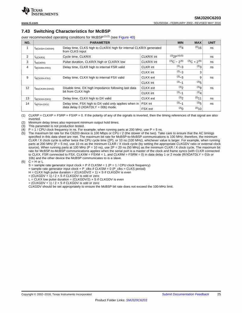
(1) CLKRP = CLKXP = FSRP = FSXP = 0. If the polarity of any of the signals is inverted, then the timing references of that signal are alsoinverted.
(2) P = 1 / CPU clock frequency in ns. For example, when running parts at 200 MHz, use P = 5 ns.(3) The maximum bit rate for the C6203 device is 100 Mbps or CPU / 2 (the slower of the two). Take care to ensure that the AC timings
specified in this data sheet are met. The maximum bit rate for McBSP-to-McBSP communications is 100 MHz; therefore, the minimumCLKR / X clock cycle is either twice the CPU cycle time (2P), or 10 ns (100 MHz), whichever value is larger. For example, when runningparts at 200 MHz (P = 5 ns), use 10 ns as the minimum CLKR/X clock cycle (by setting the appropriate CLKGDV ratio or external clocksource). When running parts at 100 MHz (P = 10 ns), use 2P = 20 ns (50 MHz) as the minimum CLKR/X clock cycle. The maximum bitrate for McBSP-to-McBSP communications applies when the serial port is a master of the clock and frame syncs (with CLKR connectedto CLKX, FSR connected to FSX, CLKXM = FSXM = 1, and CLKRM = FSRM = 0) in data delay 1 or 2 mode (R/XDATDLY = 01b or10b) and the other device the McBSP communicates to is a slave.
(4) This parameter is not production tested.(5) The minimum CLKR/X pulse duration is either (P − 1) or 4 ns, whichever is larger. For example, when running parts at 200 MHz (P = 5
ns), use 4 ns as the minimum CLKR/X pulse duration. When running parts at 100 MHz (P = 10 ns), use (P − 1) = 9 ns as the minimumCLKR/X pulse duration.
7.20 Timing Requirements for McBSPsee Figure 40 (1) (2)
NO. MIN MAX UNIT2 tc(CKRX) Cycle time, CLKR/X CLKR/X ext 2P (3) ns3 tw(CKRX) Pulse duration, CLKR/X high or CLKR/X low CLKR/X ext (4)P − 1 (5) ns
CLKR int 95 tsu(FRH-CKRL) Setup time, external FSR high before CLKR low CLKR ext 2 ns
CLKR int 66 th(CKRL-FRH) Hold time, external FSR high after CLKR low CLKR ext 4 ns
CLKR int 87 tsu(DRV-CKRL) Setup time, DR valid before CLKR low CLKR ext 0.5 ns
CLKR int 38 th(CKRL-DRV) Hold time, DR valid after CLKR low CLKR ext 5 ns
CLKX int 910 tsu(FXH-CKXL) Setup time, external FSX high before CLKX low CLKX ext 2 ns
CLKX int 611 th(CKXL-FXH) Hold time, external FSX high after CLKX low CLKX ext 4 ns
(1) This parameter is not production tested.
7.21 Timing Requirements for FSR when GSYNC = 1see Figure 41
NO. MIN MAX UNIT1 tsu(FRH-CKSH) Setup time, FSR high before CLKS high (1)4 ns2 th(CKSH-FRH) Hold time, FSR high after CLKS high (1)4 ns

18
SMJ320C6203SGUS033A –FEBRUARY 2002–REVISED MAY 2016 www.ti.com
Product Folder Links: SMJ320C6203
Submit Documentation Feedback Copyright © 2002–2016, Texas Instruments Incorporated
(1) P = 1 / CPU clock frequency in ns. For example, when running parts at 200 MHz, use P = 5 ns.(2) For all SPI slave modes, CLKG is programmed as 1/2 of the CPU clock by setting CLKSM = CLKGDV = 1.(3) This parameter is not production tested.
7.22 Timing Requirements for McBSP as SPI Master or Slave: CLKSTP = 10b, CLKXP = 0see Figure 42 (1) (2)
NO. MASTER SLAVEUNIT
MIN MAX MIN MAX4 tsu(DRV-CKXL) Setup time, DR valid before CLKX low (3)12 (3)2 − 3P ns5 th(CKXL-DRV) Hold time, DR valid after CLKX low (3)4 (3)5 + 6P ns
(1) P = 1 / CPU clock frequency in ns. For example, when running parts at 200 MHz, use P = 5 ns.(2) For all SPI slave modes, CLKG is programmed as 1/2 of the CPU clock by setting CLKSM = CLKGDV = 1.(3) This parameter is not production tested.
7.23 Timing Requirements for McBSP as SPI Master or Slave: CLKSTP = 11b, CLKXP = 0see Figure 43 (1) (2)
NO. MASTER SLAVE UNITMIN MAX MIN MAX
4 tsu(DRV-CKXH) Setup time, DR valid before CLKX high (3)12 (3)2 − 3P ns5 th(CKXH-DRV) Hold time, DR valid after CLKX high (3)4 (3)5 + 6P ns
(1) P = 1 / CPU clock frequency in ns. For example, when running parts at 200 MHz, use P = 5 ns.(2) For all SPI slave modes, CLKG is programmed as 1/2 of the CPU clock by setting CLKSM = CLKGDV = 1.(3) This parameter is not production tested.
7.24 Timing Requirements for McBSP as SPI Master or Slave: CLKSTP = 10b, CLKXP = 1see Figure 44 (1) (2)
NO. MASTER SLAVE UNITMIN MAX MIN MAX
4 tsu(DRV-CKXH) Setup time, DR valid before CLKX high (3)12 (3)2 − 3P ns5 th(CKXH-DRV) Hold time, DR valid after CLKX high (3)4 (3)5 + 6P ns
(1) P = 1 / CPU clock frequency in ns. For example, when running parts at 200 MHz, use P = 5 ns.(2) For all SPI slave modes, CLKG is programmed as 1/2 of the CPU clock by setting CLKSM = CLKGDV = 1.(3) This parameter is not production tested.
7.25 Timing Requirements for McBSP as SPI Master or Slave: CLKSTP = 11b, CLKXP = 1see Figure 45 (1) (2)
NO. MASTER SLAVE UNITMIN MAX MIN MAX
4 tsu(DRV-CKXL) Setup time, DR valid before CLKX low (3)12 (3)2 − 3P ns5 th(CKXL-DRV) Hold time, DR valid after CLKX low (3)4 (3)5 + 6P ns
(1) P = 1 / CPU clock frequency in ns. For example, when running parts at 200 MHz, use P = 5 ns(2) This parameter is not production tested.
7.26 Timing Requirements for Timer Inputssee Figure 47 (1)
NO. MIN MAX UNIT1 tw(TINPH) Pulse duration, TINP high (2)2P ns2 tw(TINPL) Pulse duration, TINP low (2)2P ns

19
SMJ320C6203www.ti.com SGUS033A –FEBRUARY 2002–REVISED MAY 2016
Product Folder Links: SMJ320C6203
Submit Documentation FeedbackCopyright © 2002–2016, Texas Instruments Incorporated
(1) This parameter is not production tested.
7.27 Timing Requirements for JTAG Test Portsee Figure 49
NO. MIN MAX UNIT1 tc(TCK) Cycle time, TCK (1)35 ns3 tsu(TDIV-TCKH) Setup time, TDI/TMS/TRST valid before TCK high (1)11 ns4 th(TCKH-TDIV) Hold time, TDI/TMS/TRST valid after TCK high (1)9 ns

20
SMJ320C6203SGUS033A –FEBRUARY 2002–REVISED MAY 2016 www.ti.com
Product Folder Links: SMJ320C6203
Submit Documentation Feedback Copyright © 2002–2016, Texas Instruments Incorporated
(1) P = 1 / CPU clock frequency in ns.(2) The reference points for the rise and fall transitions are measured at VOL MAX and VOH MIN.(3) This parameter is not production tested.
7.28 Switching Characteristics for CLKOUT2over recommended operating conditions for CLKOUT2 (1) (2) (see Figure 7)
NO. PARAMETER MIN MAX UNIT1 tc(CKO2) Cycle time, CLKOUT2 (3)2P − 0.7 (3)2P + 0.7 ns2 tw(CKO2H) Pulse duration, CLKOUT2 high (3)P − 0.7 (3)P + 0.7 ns3 tw(CKO2L) Pulse duration, CLKOUT2 low (3)P − 0.7 (3)P + 0.7 ns
(1) P = 1 / CPU clock frequency in ns.(2) D = 8, 6, 4, or 2; FIFO clock divide ratio, user-programmable(3) This parameter is not production tested.
7.29 Switching Characteristics for XFCLKover recommended operating conditions for XFCLK (1) (2) (see Figure 8)
NO. PARAMETER MIN MAX UNIT1 tc(XFCK) Cycle time, XFCLK (3)D × P − 0.7 (3)D × P + 0.7 ns2 tw(XFCKH) Pulse duration, XFCLK high (3)(D/2) × P − 0.7 (3)(D/2) × P + 0.7 ns3 tw(XFCKL) Pulse duration, XFCLK low (3)(D/2) × P − 0.7 (3)(D/2) × P + 0.7 ns
(1) RS = Read setup, RST = Read strobe, RH = Read hold, WS = Write setup, WST = Write strobe, WH = Write hold. These parametersare programmed by the EMIF CE space control registers.
(2) P = 1 / CPU clock frequency in ns. For example, when running parts at 200 MHz, use P = 5 ns.(3) The sum of RS and RST (or WS and WST) must be a minimum of 4 to use ARDY input to extend strobe width.(4) Select signals include: CEx, BE[3:0], EA[21:2], AOE; and for writes, include ED[31:0], with the exception that CEx can stay active for an
additional 7P ns following the end of the cycle.(5) This parameter is not production tested.
7.30 Asynchronous Memory Timing Switching Characteristicsover recommended operating conditions for asynchronous memory cycles (1) (2) (3) (4) (see Figure 9 through Figure 12)
NO. PARAMETER MIN TYP MAX UNIT1 tosu(SELV-AREL) Output setup time, select signals valid to ARE low RS × P − 2 ns2 toh(AREH-SELIV) Output hold time, ARE high to select signals invalid (5)RH × P −
2ns
5 tw(AREL) Pulse duration, ARE low RST × P ns8 td(ARDYH-AREH) Delay time, ARDY high to ARE high (5)3P (5)4P + 5 ns12 tosu(SELV-AWEL) Output setup time, select signals valid to AWE low WS × P − 3 ns13 toh(AWEH-SELIV) Output hold time, AWE high to select signals invalid (5)WH × P −
2ns
14 tw(AWEL) Pulse duration, AWE low WST × P ns17 td(ARDYH-AWEH) Delay time, ARDY high to AWE high (5)3P (5)4P + 5 ns

21
SMJ320C6203www.ti.com SGUS033A –FEBRUARY 2002–REVISED MAY 2016
Product Folder Links: SMJ320C6203
Submit Documentation FeedbackCopyright © 2002–2016, Texas Instruments Incorporated
(1) P = 1 / CPU clock frequency in ns. For example, when running parts at 200 MHz, use P = 5 ns.(2) SDCAS/SSADS, SDRAS/SSOE, and SDWE/SSWE operate as SSADS, SSOE, and SSWE, respectively, during SBSRAM accesses.(3) This parameter is not production tested.(4) For the first write in a series of one or more consecutive adjacent writes, the write data is generated one CLKOUT2 cycle early to
accommodate the ED enable time.
7.31 Switching Characteristics for Synchronous-Burst SRAM Cyclesover recommended operating conditions for synchronous-burst SRAM cycles (1) (2) (see Figure 13 and Figure 14)
NO. PARAMETER MIN MAX UNIT1 tosu(CEV-CKO2H) Output setup time, CEx valid before CLKOUT2 high P − 1.7 ns2 toh(CKO2H-CEV) Output hold time, CEx valid after CLKOUT2 high (3)P − 4 ns3 tosu(BEV-CKO2H) Output setup time, BEx valid before CLKOUT2 high P − 1.7 ns4 toh(CKO2H-BEIV) Output hold time, BEx invalid after CLKOUT2 high (3)P − 4 ns5 tosu(EAV-CKO2H) Output setup time, EAx valid before CLKOUT2 high P − 1.7 ns6 toh(CKO2H-EAIV) Output hold time, EAx invalid after CLKOUT2 high (3)P − 4 ns9 tosu(ADSV-CKO2H) Output setup time, SDCAS/SSADS valid before CLKOUT2 high P − 1.7 ns10 toh(CKO2H-ADSV) Output hold time, SDCAS/SSADS valid after CLKOUT2 high (3)P − 4 ns11 tosu(OEV-CKO2H) Output setup time, SDRAS/SSOE valid before CLKOUT2 high P − 1.7 ns12 toh(CKO2H-OEV) Output hold time, SDRAS/SSOE valid after CLKOUT2 high (3)P − 4 ns13 tosu(EDV-CKO2H) Output setup time, EDx valid before CLKOUT2 high (4) P − 2.3 ns14 toh(CKO2H-EDIV) Output hold time, EDx invalid after CLKOUT2 high (3)P − 4 ns15 tosu(WEV-CKO2H) Output setup time, SDWE/SSWE valid before CLKOUT2 high P − 1.7 ns16 toh(CKO2H-WEV) Output hold time, SDWE/SSWE valid after CLKOUT2 high (3)P − 4 ns
(1) P = 1 / CPU clock frequency in ns. For example, when running parts at 200 MHz, use P = 5 ns.(2) SDCAS/SSADS, SDRAS/SSOE, and SDWE/SSWE operate as SDCAS, SDRAS, and SDWE, respectively, during SDRAM accesses.(3) This parameter is not production tested.(4) For the first write in a series of one or more consecutive adjacent writes, the write data is generated one CLKOUT2 cycle early to
accommodate the ED enable time.
7.32 Switching Characteristics for Synchronous DRAM Cyclesover recommended operating conditions for synchronous DRAM cycles for C6203B Rev. 2 (1) (2) (see Figure 15 throughFigure 20)
NO. PARAMETER MIN MAX UNIT1 tosu(CEV-CKO2H) Output setup time, CEx valid before CLKOUT2 high P − 0.9 ns2 toh(CKO2H-CEV) Output hold time, CEx valid after CLKOUT2 high (3)P − 4.1 ns3 tosu(BEV-CKO2H) Output setup time, BEx valid before CLKOUT2 high P − 0.9 ns4 toh(CKO2H-BEIV) Output hold time, BEx invalid after CLKOUT2 high (3)P − 4.1 ns5 tosu(EAV-CKO2H) Output setup time, EAx valid before CLKOUT2 high P − 0.9 ns6 toh(CKO2H-EAIV) Output hold time, EAx invalid after CLKOUT2 high (3)P − 4.1 ns9 tosu(CASV-CKO2H) Output setup time, SDCAS/SSADS valid before CLKOUT2 high P − 0.9 ns10 toh(CKO2H-CASV) Output hold time, SDCAS/SSADS valid after CLKOUT2 high (3)P − 4.1 ns11 tosu(EDV-CKO2H) Output setup time, EDx valid before CLKOUT2 high (4) P − 1.5 ns12 toh(CKO2H-EDIV) Output hold time, EDx invalid after CLKOUT2 high (3)P − 4.1 ns13 tosu(WEV-CKO2H) Output setup time, SDWE/SSWE valid before CLKOUT2 high P − 0.9 ns14 toh(CKO2H-WEV) Output hold time, SDWE/SSWE valid after CLKOUT2 high (3)P − 4.1 ns15 tosu(SDA10V-CKO2H) Output setup time, SDA10 valid before CLKOUT2 high P − 0.9 ns16 toh(CKO2H-SDA10IV) Output hold time, SDA10 invalid after CLKOUT2 high (3)P − 4.1 ns17 tosu(RASV-CKO2H) Output setup time, SDRAS/SSOE valid before CLKOUT2 high P − 0.9 ns18 toh(CKO2H-RASV) Output hold time, SDRAS/SSOE valid after CLKOUT2 high (3)P − 4.1 ns

22
SMJ320C6203SGUS033A –FEBRUARY 2002–REVISED MAY 2016 www.ti.com
Product Folder Links: SMJ320C6203
Submit Documentation Feedback Copyright © 2002–2016, Texas Instruments Incorporated
(1) P = 1 / CPU clock frequency in ns. For example, when running parts at 200 MHz, use P = 5 ns.(2) EMIF bus consists of CE[3:0], BE[3:0], ED[31:0], EA[21:2], ARE, AOE, AWE, SDCAS/ SSADS, SDRAS/SSOE, SDWE/SSWE, and
SDA10.(3) This parameter is not production tested.(4) All pending EMIF transactions are allowed to complete before HOLDA is asserted. The worst case for this is an asynchronous read or
write with external ARDY used or a minimum of eight consecutive SDRAM reads or writes when RBTR8 = 1. If no bus transactions areoccurring, then the minimum delay time can be achieved. Also, bus hold can be indefinitely delayed by setting NOHOLD = 1.
7.33 Switching Characteristics for the HOLD/HOLDA Cyclesover recommended operating conditions for the HOLD/HOLDA cycles (1) (2) (see Figure 21)
NO. PARAMETER MIN MAX UNIT1 td(HOLDL-EMHZ) Delay time, HOLD low to EMIF bus high impedance (3)3P (4) ns2 td(EMHZ-HOLDAL) Delay time, EMIF bus high impedance to HOLDA low (3)0 (3)2P ns4 td(HOLDH-EMLZ) Delay time, HOLD high to EMIF bus low impedance (3)3P (3)7P ns5 td(EMLZ-HOLDAH) Delay time, EMIF bus low impedance to HOLDA high (3)0 (3)2P ns
(1) P = 1 / CPU clock frequency in ns. For example, when running parts at 200 MHz, use P = 5 ns.(2) High group consists of: XFCLK, HOLDA
Low group consists of: IACK, INUM[3:0], DMAC[3:0], PD, TOUT0, and TOUT1Z group consists of: EA[21:2], ED[31:0], CE[3:0], BE[3:0], ARE, AWE, AOE, SDCAS/SSADS, SDRAS/SSOE, SDWE/SSWE, SDA10,CLKX0, CLKX1, CLKX2, FSX0, FSX1, FSX2, DX0, DX1, DX2, CLKR0, CLKR1, CLKR2, FSR0, FSR1, FSR2, XCE[3:0],XBE[3:0]/XA[5:2], XOE, XRE, XWE/XWAIT, XAS, XW/R, XRDY, XBLAST, XHOLD, and XHOLDA
(3) This parameter is not production tested.
7.34 Switching Characteristics for Resetover recommended operating conditions during reset (1) (2) (see Figure 22)
NO. PARAMETER MIN MAX UNIT2 td(RSTL-CKO2IV) Delay time, RESET low to CLKOUT2 invalid (3)P ns3 td(RSTH-CKO2V) Delay time, RESET high to CLKOUT2 valid (3)4P ns4 td(RSTL-HIGHIV) Delay time, RESET low to high group invalid (3)P ns5 td(RSTH-HIGHV) Delay time, RESET high to high group valid (3)4P ns6 td(RSTL-LOWIV) Delay time, RESET low to low group invalid (3)P ns7 td(RSTH-LOWV) Delay time, RESET high to low group valid (3)4P ns8 td(RSTL-ZHZ) Delay time, RESET low to Z group high impedance (3)P ns9 td(RSTH-ZV) Delay time, RESET high to Z group valid (3)4P ns
(1) P = 1 / CPU clock frequency in ns. For example, when running parts at 200 MHz, use P = 5 ns.(2) When CLKOUT2 is in half mode (see CLKOUT2 in ), timings are based on falling edges.(3) This parameter is not production tested.
7.35 Switching Characteristics for Interrupt Response Cyclesover recommended operating conditions during interrupt response cycles (1) (2) (see Figure 23)
NO. PARAMETER MIN MAX UNIT1 tR(EINTH − IACKH) Response time, EXT_INTx high to IACK high (3)9P ns4 td(CKO2L-IACKV) Delay time, CLKOUT2 low to IACK valid (3)−1.5 (3)10 ns5 td(CKO2L-INUMV) Delay time, CLKOUT2 low to INUMx valid (3)−2.0 (3)10 ns6 td(CKO2L-INUMIV) Delay time, CLKOUT2 low to INUMx invalid (3)−2.0 (3)10 ns

23
SMJ320C6203www.ti.com SGUS033A –FEBRUARY 2002–REVISED MAY 2016
Product Folder Links: SMJ320C6203
Submit Documentation FeedbackCopyright © 2002–2016, Texas Instruments Incorporated
(1) This parameter is not production tested.(2) XBE[3:0]/XA[5:2] operate as address signals XA[5:2] during synchronous FIFO accesses.(3) XWE/XWAIT operates as the write-enable signal XWE during synchronous FIFO accesses.
7.36 Switching Characteristics for Synchronous FIFO Interfaceover recommended operating conditions for synchronous FIFO interface (see Figure 24 through Figure 26)
NO. PARAMETER MIN MAX UNIT1 td(XFCKH-XCEV) Delay time, XFCLK high to XCEx valid (1)−1.5 4.5 ns2 td(XFCKH-XAV) Delay time, XFCLK high to XBE[3:0]/XA[5:2] valid (2) (1)−1.5 4.5 ns3 td(XFCKH-XOEV) Delay time, XFCLK high to XOE valid (1)−1.5 4.5 ns4 td(XFCKH-XREV) Delay time, XFCLK high to XRE valid (1)−1.5 4.5 ns7 td(XFCKH-XWEV) Delay time, XFCLK high to XWE/XWAIT (3) valid (1)−1.5 4.5 ns8 td(XFCKH-XDV) Delay time, XFCLK high to XDx valid 4.5 ns9 td(XFCKH-XDIV) Delay time, XFCLK high to XDx invalid (1)−1.5 ns
(1) RS = Read setup, RST = Read strobe, RH = Read hold, WS = Write setup, WST = Write strobe, WH = Write hold. These parametersare programmed by the expansion bus XCE space control registers.
(2) P = 1 / CPU clock frequency in ns. For example, when running parts at 200 MHz, use P = 5 ns.(3) The sum of RS and RST (or WS and WST) must be a minimum of 4 to use XRDY input to extend strobe width.(4) Select signals include: XCEx, XBE[3:0]/XA[5:2], XOE; and for writes, include XD[31:0], with the exception that XCEx can stay active for
an additional 7P ns following the end of the cycle.(5) This parameter is not production tested.
7.37 Switching Characteristics for Asynchronous Peripheral Cyclesover recommended operating conditions for asynchronous peripheral cycles (1) (2) (3) (4) (see Figure 27 through Figure 30)
NO. PARAMETER MIN TYP MAX UNIT1 tosu(SELV-XREL) Output setup time, select signals valid to XRE low RS × P − 2 ns2 toh(XREH-SELIV) Output hold time, XRE low to select signals invalid (5)RH × P − 2 ns5 tw(XREL) Pulse duration, XRE low RST × P ns8 td(XRDYH-XREH) Delay time, XRDY high to XRE high (5)3P (5)4P + 5 ns12 tosu(SELV-XWEL) Output setup time, select signals valid to XWE low WS × P − 3 ns13 toh(XWEH-SELIV) Output hold time, XWE low to select signals invalid (5)WH × P −
2ns
14 tw(XWEL) Pulse duration, XWE low WST x P ns17 td(XRDYH-XWEH) Delay time, XRDY high to XWE high (5)3P (5)4P + 5 ns
(1) P = 1 / CPU clock frequency in ns. For example, when running parts at 200 MHz, use P = 5 ns.(2) This parameter is not production tested.(3) XRDY operates as active-low ready input/output during host-port accesses.
7.38 Switching Characteristics With External Device as Bus Masterover recommended operating conditions with external device as bus master (1) (see Figure 31 and Figure 32)
NO. PARAMETER MIN MAX UNIT11 td(XCKIH-XDLZ) Delay time, XCLKIN high to XDx low impedance (2)0 ns12 td(XCKIH-XDV) Delay time, XCLKIN high to XDx valid 4P ns13 td(XCKIH-XDIV) Delay time, XCLKIN high to XDx invalid (2)5 ns14 td(XCKIH-XDHZ) Delay time, XCLKIN high to XDx high impedance (2)4P ns15 td(XCKIH-XRY) Delay time, XCLKIN high to XRDY invalid (3) (2)5 (2)4P ns20 td(XCKIH-XRYLZ) Delay time, XCLKIN high to XRDY low impedance (2)5 (2)4P ns21 td(XCKIH-XRYHZ) Delay time, XCLKIN high to XRDY high impedance (3) (2)2P + 5 (2)7P ns

24
SMJ320C6203SGUS033A –FEBRUARY 2002–REVISED MAY 2016 www.ti.com
Product Folder Links: SMJ320C6203
Submit Documentation Feedback Copyright © 2002–2016, Texas Instruments Incorporated
(1) P = 1 / CPU clock frequency in ns. For example, when running parts at 200 MHz, use P = 5 ns.(2) This parameter is not production tested.(3) XW/R input/output polarity selected at boot.(4) XBLAST output polarity is always active low.(5) XBE[3:0]/XA[5:2] operate as byte-enables XBE[3:0] during host-port accesses.(6) XWE/XWAIT operates as XWAIT output signal during host-port accesses.
7.39 Switching Characteristics With C62x as Bus Masterover recommended operating conditions with C62x as bus master (1) (see Figure 33 through Figure 35)NO. PARAMETER MIN MAX UNIT1 td(XCKIH-XASV) Delay time, XCLKIN high to XAS valid (2)5 4P ns2 td(XCKIH-XWRV) Delay time, XCLKIN high to XW/R valid (3) (2)5 4P ns3 td(XCKIH-XBLTV) Delay time, XCLKIN high to XBLAST valid (4) (2)5 4P ns4 td(XCKIH-XBEV) Delay time, XCLKIN high to XBE[3:0]/XA[5:2] valid (5) (2)5 4P ns5 td(XCKIH-XDLZ) Delay time, XCLKIN high to XDx low impedance (2)0 ns6 td(XCKIH-XDV) Delay time, XCLKIN high to XDx valid 4P ns7 td(XCKIH-XDIV) Delay time, XCLKIN high to XDx invalid (2)5 ns8 td(XCKIH-XDHZ) Delay time, XCLKIN high to XDx high impedance (2)4P ns13 td(XCKIH-XWTV) Delay time, XCLKIN high to XWE/XWAIT valid (6) (2)5 4P ns
(1) P = 1 / CPU clock frequency in ns. For example, when running parts at 200 MHz, use P = 5 ns.(2) This parameter is not production tested.
7.40 Switching Characteristics With External Device as Asynchronous Bus Masterover recommended operating conditions with external device as asynchronous bus master (1) (see Figure 36 and Figure 37)
NO. PARAMETER MIN MAX UNIT5 td(XCSL-XDLZ) Delay time, XCS low to XDx low impedance (2)0 ns6 td(XCSH-XDIV) Delay time, XCS high to XDx invalid (2)0 (2)12 ns7 td(XCSH-XDHZ) Delay time, XCS high to XDx high impedance (2)4P ns8 td(XRYL-XDV) Delay time, XRDY low to XDx valid (2)−4 (2)1 ns9 td(XCSH-XRYH) Delay time, XCS high to XRDY high (2)0 12 ns
(1) P = 1 / CPU clock frequency in ns. For example, when running parts at 200 MHz, use P = 5 ns.(2) Expansion bus consists of XBE[3:0]/XA[5:2], XAS, XW/R, and XBLAST.(3) This parameter is not production tested.(4) All pending expansion bus transactions are allowed to complete before XHOLDA is asserted.
7.41 Switching Characteristics for Expansion Bus Arbitration (Internal Arbiter Enabled)over recommended operating conditions for expansion bus arbitration (internal arbiter enabled) (1) (2) (see Figure 38)
NO. PARAMETER MIN MAX UNIT1 td(XHDH-XBHZ) Delay time, XHOLD high to expansion bus high impedance (3)3P (4) ns2 td(XBHZ-XHDAH) Delay time, expansion bus high impedance to XHOLDA high (3)0 (3)2P ns4 td(XHDL-XHDAL) Delay time, XHOLD low to XHOLDA low (3)3P ns5 td(XHDAL-XBLZ) Delay time, XHOLDA low to expansion bus low impedance (3)0 (3)2P ns
(1) P = 1 / CPU clock frequency in ns. For example, when running parts at 200 MHz, use P = 5 ns.(2) Expansion bus consists of XBE[3:0]/XA[5:2], XAS, XW/R, and XBLAST.(3) This parameter is not production tested.
7.42 Switching Characteristics for Expansion Bus Arbitration (Internal Arbiter Disabled)over recommended operating conditions for expansion bus arbitration (internal arbiter disabled) (1) (see Figure 39)
NO. PARAMETER MIN MAX UNIT1 td(XHDAH-XBLZ) Delay time, XHOLDA high to expansion bus low impedance (2) (3)2P (3)2P + 10 ns2 td(XBHZ-XHDL) Delay time, expansion bus high impedance to XHOLD low (2) (3)0 (3)2P ns
25
SMJ320C6203www.ti.com SGUS033A –FEBRUARY 2002–REVISED MAY 2016
Product Folder Links: SMJ320C6203
Submit Documentation FeedbackCopyright © 2002–2016, Texas Instruments Incorporated
(1) CLKRP = CLKXP = FSRP = FSXP = 0. If the polarity of any of the signals is inverted, then the timing references of that signal are alsoinverted.
(2) Minimum delay times also represent minimum output hold times.(3) This parameter is not production tested.(4) P = 1 / CPU clock frequency in ns. For example, when running parts at 200 MHz, use P = 5 ns.(5) The maximum bit rate for the C6203 device is 100 Mbps or CPU / 2 (the slower of the two). Take care to ensure that the AC timings
specified in this data sheet are met. The maximum bit rate for McBSP-to-McBSP communications is 100 MHz; therefore, the minimumCLKR / X clock cycle is either twice the CPU cycle time (2P), or 10 ns (100 MHz), whichever value is larger. For example, when runningparts at 200 MHz (P = 5 ns), use 10 ns as the minimum CLKR / X clock cycle (by setting the appropriate CLKGDV ratio or external clocksource). When running parts at 100 MHz (P = 10 ns), use 2P = 20 ns (50 MHz) as the minimum CLKR / X clock cycle. The maximum bitrate for McBSP-to-McBSP communications applies when the serial port is a master of the clock and frame syncs (with CLKR connectedto CLKX, FSR connected to FSX, CLKXM = FSXM = 1, and CLKRM = FSRM = 0) in data delay 1 or 2 mode (R/XDATDLY = 01b or10b) and the other device the McBSP communicates to is a slave.
(6) C = H or LS = sample rate generator input clock = P if CLKSM = 1 (P = 1 / CPU clock frequency)= sample rate generator input clock = P_clks if CLKSM = 0 (P_clks = CLKS period)H = CLKX high pulse duration = (CLKGDV/2 + 1) × S if CLKGDV is even= (CLKGDV + 1) / 2 × S if CLKGDV is odd or zeroL = CLKX low pulse duration = (CLKGDV/2) × S if CLKGDV is even= (CLKGDV + 1) / 2 × S if CLKGDV is odd or zeroCLKGDV should be set appropriately to ensure the McBSP bit rate does not exceed the 100-MHz limit.
7.43 Switching Characteristics for McBSPover recommended operating conditions for McBSP (1) (2) (see Figure 40)
NO. PARAMETER MIN MAX UNIT1 td(CKSH-CKRXH) Delay time, CLKS high to CLKR/X high for internal CLKR/X generated
from CLKS input(3)4 (3)16 ns
2 tc(CKRX) Cycle time, CLKR/X CLKR/X int (3)2P (4) (5) ns3 tw(CKRX) Pulse duration, CLKR/X high or CLKR/X low CLKR/X int (3)C − 2 (6) (3)C + 2(6) ns4 td(CKRH-FRV) Delay time, CLKR high to internal FSR valid CLKR int (3)−3 (3)3 ns
CLKX int (3)−3 39 td(CKXH-FXV) Delay time, CLKX high to internal FSX valid CLKX ext (3)−3 9 ns
CLKX int (3)−1 (3)512 tdis(CKXH-DXHZ) Disable time, DX high impedance following last data
bit from CLKX highCLKX ext (3)2 (3)9 nsCLKX int (3)−1 (3)4
13 td(CKXH-DXV) Delay time, CLKX high to DX valid CLKX ext (3)2 (3)11 ns14 td(FXH-DXV) Delay time, FSX high to DX valid only applies when in
data delay 0 (XDATDLY = 00b) mode.FSX int (3)−1 (3)5 nsFSX ext (3)0 (3)10

26
SMJ320C6203SGUS033A –FEBRUARY 2002–REVISED MAY 2016 www.ti.com
Product Folder Links: SMJ320C6203
Submit Documentation Feedback Copyright © 2002–2016, Texas Instruments Incorporated
(1) P = 1 / CPU clock frequency in ns. For example, when running parts at 200 MHz, use P = 5 ns.(2) For all SPI slave modes, CLKG is programmed as 1/2 of the CPU clock by setting CLKSM = CLKGDV = 1.(3) S = sample rate generator input clock = P if CLKSM = 1 (P = 1 / CPU clock frequency)
= sample rate generator input clock = P_clks if CLKSM = 0 (P_clks = CLKS period)T = CLKX period = (1 + CLKGDV) × SH = CLKX high pulse duration = (CLKGDV / 2 + 1) × S if CLKGDV is even= (CLKGDV + 1) / 2 × S if CLKGDV is odd or zeroL = CLKX low pulse duration = (CLKGDV / 2) × S if CLKGDV is even= (CLKGDV + 1) / 2 × S if CLKGDV is odd or zeroCLKGDV should be set appropriately to ensure the McBSP bit rate does not exceed the 100-MHz limit.
(4) FSRP = FSXP = 1. As a SPI master, FSX is inverted to provide active-low slave-enable output. As a slave, the active-low signal input onFSX and FSR is inverted before being used internally. CLKXM = FSXM = 1, CLKRM = FSRM = 0 for master McBSP CLKXM = CLKRM= FSXM = FSRM = 0 for slave McBSP
(5) This parameter is not production tested.(6) FSX should be low before the rising edge of clock to enable slave devices and then begin a SPI transfer at the rising edge of the master
clock (CLKX).
7.44 Switching Characteristics for McBSP as SPI Master or Slaveover recommended operating conditions for McBSP as SPI master or slave: CLKSTP = 10b, CLKXP = 0 (1) (2) (see Figure 42)
NO. PARAMETER MASTER (3) SLAVE UNITMIN MAX MIN MAX
1 th(CKXL-FXL) Hold time, FSX low after CLKX low (4) (5)T − 2 (5)T + 3 ns2 td(FXL-CKXH) Delay time, FSX low to CLKX high (6) (5)L − 2 (5)L + 3 ns3 td(CKXH-DXV) Delay time, CLKX high to DX valid (5)−4 (5)4 (5)3P + 4 (5)5P + 17 ns6 tdis(CKXL-DXHZ) Disable time, DX high impedance following last
data bit from CLKX low(5)L − 2 (5)L + 3 ns
7 tdis(FXH-DXHZ) Disable time, DX high impedance following lastdata bit from FSX high
(5)P + 3 (5)3P + 17 ns
8 td(FXL-DXV) Delay time, FSX low to DX valid (5)2P + 2 (5)4P + 17 ns
(1) P = 1 / CPU clock frequency in ns. For example, when running parts at 200 MHz, use P = 5 ns.(2) For all SPI slave modes, CLKG is programmed as 1/2 of the CPU clock by setting CLKSM = CLKGDV = 1.(3) S = Sample rate generator input clock = P if CLKSM = 1 (P = 1 / CPU clock frequency)
= Sample rate generator input clock = P_clks if CLKSM = 0 (P_clks = CLKS period)T = CLKX period = (1 + CLKGDV) × SH = CLKX high pulse duration = (CLKGDV / 2 + 1) × S if CLKGDV is even= (CLKGDV + 1) / 2 × S if CLKGDV is odd or zeroL = CLKX low pulse duration = (CLKGDV / 2) × S if CLKGDV is even= (CLKGDV + 1) / 2 × S if CLKGDV is odd or zeroThe maximum transfer rate for SPI mode is limited to the above AC timing constraints.
(4) FSRP = FSXP = 1. As a SPI master, FSX is inverted to provide active-low slave-enable output. As a slave, the active-low signal input onFSX and FSR is inverted before being used internally. CLKXM = FSXM = 1, CLKRM = FSRM = 0 for master McBSP CLKXM = CLKRM= FSXM = FSRM = 0 for slave McBSP
(5) This parameter is not production tested.(6) FSX should be low before the rising edge of clock to enable slave devices and then begin a SPI transfer at the rising edge of the master
clock (CLKX).
7.45 Switching Characteristics for McBSP as SPI Master or Slave: CLKSTP = 11b, CLKXP = 0over recommended operating conditions for McBSP as SPI master or slave: CLKSTP = 11b, CLKXP = 0 (1) (2) (see Figure 43)
NO. PARAMETER MASTER (3) SLAVE UNITMIN MAX MIN MAX
1 th(CKXL-FXL) Hold time, FSX low after CLKX low (4) (5)L − 2 (5)L + 3 ns2 td(FXL-CKXH) Delay time, FSX low to CLKX high (6) (5)T − 2 (5)T + 3 ns3 td(CKXL-DXV) Delay time, CLKX low to DX valid (5)−4 (5)4 (5)3P + 4 (5)5P + 17 ns6 tdis(CKXL-DXHZ) Disable time, DX high impedance following last
data bit from CLKX low(5)−2 (5)4 (5)3P + 3 (5)5P + 17 ns
7 td(FXL-DXV) Delay time, FSX low to DX valid (5)H − 2 (5)H + 4 (5)2P + 2 (5)4P + 17 ns

27
SMJ320C6203www.ti.com SGUS033A –FEBRUARY 2002–REVISED MAY 2016
Product Folder Links: SMJ320C6203
Submit Documentation FeedbackCopyright © 2002–2016, Texas Instruments Incorporated
(1) P = 1 / CPU clock frequency in ns. For example, when running parts at 200 MHz, use P = 5 ns.(2) For all SPI slave modes, CLKG is programmed as 1/2 of the CPU clock by setting CLKSM = CLKGDV = 1.(3) S = Sample rate generator input clock = P if CLKSM = 1 (P = 1 / CPU clock frequency)
= Sample rate generator input clock = P_clks if CLKSM = 0 (P_clks = CLKS period)T = CLKX period = (1 + CLKGDV) × SH = CLKX high pulse duration = (CLKGDV / 2 + 1) × S if CLKGDV is even = (CLKGDV + 1) / 2 × S if CLKGDV is odd or zeroL = CLKX low pulse duration = (CLKGDV / 2) × S if CLKGDV is even = (CLKGDV + 1) / 2 × S if CLKGDV is odd or zeroThe maximum transfer rate for SPI mode is limited to the above AC timing constraints.
(4) FSRP = FSXP = 1. As a SPI master, FSX is inverted to provide active-low slave-enable output. As a slave, the active-low signal input onFSX and FSR is inverted before being used internally. CLKXM = FSXM = 1, CLKRM = FSRM = 0 for master McBSP CLKXM = CLKRM= FSXM = FSRM = 0 for slave McBSP
(5) This parameter is not production tested.(6) FSX should be low before the rising edge of clock to enable slave devices and then begin a SPI transfer at the rising edge of the master
clock (CLKX).
7.46 Switching Characteristics for McBSP as SPI Master or Slave: CLKSTP = 10b, CLKXP = 1over recommended operating conditions for McBSP as SPI master or slave: CLKSTP = 10b, CLKXP = 1 (1) (2) (see Figure 44)NO. PARAMETER MASTER (3) SLAVE UNIT
MIN MAX MIN MAX1 th(CKXH-FXL) Hold time, FSX low after CLKX high (4) (5)T − 2 (5)T + 3 ns2 td(FXL-CKXL) Delay time, FSX low to CLKX low (6) (5)H − 2 (5)H + 3 ns3 td(CKXL-DXV) Delay time, CLKX low to DX valid (5)−4 (5)4 (5)3P + 4 (5)5P + 17 ns6 tdis(CKXH-DXHZ) Disable time, DX high impedance following
last data bit from CLKX high(5)H − 2 (5)H + 3 ns
7 tdis(FXH-DXHZ) Disable time, DX high impedance followinglast data bit from FSX high
(5)P + 3 (5)3P + 17 ns
8 td(FXL-DXV) Delay time, FSX low to DX valid (5)2P + 2 (5)4P + 17 ns
(1) P = 1 / CPU clock frequency in ns. For example, when running parts at 200 MHz, use P = 5 ns.(2) For all SPI slave modes, CLKG is programmed as 1/2 of the CPU clock by setting CLKSM = CLKGDV = 1.(3) S = Sample rate generator input clock = P if CLKSM = 1 (P = 1 / CPU clock frequency)
= Sample rate generator input clock = P_clks if CLKSM = 0 (P_clks = CLKS period)T = CLKX period = (1 + CLKGDV) × SH = CLKX high pulse duration = (CLKGDV / 2 + 1) × S if CLKGDV is even= (CLKGDV + 1) / 2 × S if CLKGDV is odd or zeroL = CLKX low pulse duration = (CLKGDV / 2) × S if CLKGDV is even= (CLKGDV + 1) / 2 × S if CLKGDV is odd or zero CLKGDV should be set appropriately to ensure the McBSP bit rate does not exceedthe 100-MHz limit.
(4) FSRP = FSXP = 1. As a SPI master, FSX is inverted to provide active-low slave-enable output. As a slave, the active-low signal input onFSX and FSR is inverted before being used internally. CLKXM = FSXM = 1, CLKRM = FSRM = 0 for master McBSP CLKXM = CLKRM= FSXM = FSRM = 0 for slave McBSP
(5) This parameter is not production tested.(6) FSX should be low before the rising edge of clock to enable slave devices and then begin a SPI transfer at the rising edge of the master
clock (CLKX).
7.47 Switching Characteristics for McBSP as SPI Master or Slave: CLKSTP = 11b, CLKXP = 1for McBSP as SPI master or slave: CLKSTP = 11b, CLKXP = 1 (1) (2) (see Figure 45)
NO. PARAMETER MASTER (3) SLAVE UNITMIN MAX MIN MAX
1 th(CKXH-FXL) Hold time, FSX low after CLKX high (4) (5)H − 2 (5)H + 3 ns2 td(FXL-CKXL) Delay time, FSX low to CLKX low (6) (5)T − 2 (5)T + 2 ns3 td(CKXH-DXV) Delay time, CLKX high to DX valid (5)−4 (5)4 (5)3P + 4 (5)5P + 17 ns6 tdis(CKXH-DXHZ) Disable time, DX high impedance following
last data bit from CLKX height(5)−2 (5)4 (5)3P + 3 (5)5P + 17 ns
7 td(FXL-DXV) Delay time, FSX low to DX valid (5)L − 2 (5)L + 5 (5)2P + 2 (5)4P + 17 ns

28
SMJ320C6203SGUS033A –FEBRUARY 2002–REVISED MAY 2016 www.ti.com
Product Folder Links: SMJ320C6203
Submit Documentation Feedback Copyright © 2002–2016, Texas Instruments Incorporated
(1) P = 1 / CPU clock frequency in ns. For example, when running parts at 200 MHz, use P = 5 ns.(2) This parameter is not production tested.
7.48 Switching Characteristics for DMAC Outputsover recommended operating conditions for DMAC outputs (1) (see Figure 46)
NO. PARAMETER MIN MAX UNIT1 tw(DMACH) Pulse duration, DMAC high (2)2P − 3 ns
(1) P = 1 / CPU clock frequency in ns. For example, when running parts at 200 MHz, use P = 5 ns.(2) This parameter is not production tested.
7.49 Switching Characteristics for Timer Outputsover recommended operating conditions for timer outputs (1) (see Figure 47)
NO. PARAMETER MIN MAX UNIT3 tw(TOUTH) Pulse duration, TOUT high (2)2P − 3 ns4 tw(TOUTL) Pulse duration, TOUT low (2)2P − 3 ns
(1) P = 1 / CPU clock frequency in ns. For example, when running parts at 200 MHz, use P = 5 ns.(2) This parameter is not production tested.
7.50 Switching Characteristics for Power-Down Outputsover recommended operating conditions for power-down outputs (1) (see Figure 48)
NO. PARAMETER MIN MAX UNIT1 tw(PDH) Pulse duration, PD high (2)2P−3 ns
(1) This parameter is not production tested.
7.51 Switching Characteristics for JTAG Test Portover recommended operating conditions for JTAG test port (see Figure 49)
NO. PARAMETER MIN MAX UNIT2 td(TCKL-TDOV) Delay time, TCK low to TDO valid (1)−4.5 (1)13.5 ns

Vref = VIL MAX (or V OL MAX)
Vref = VIH MIN (or VOH MIN)
Vref = 1.5 V
Tester PinElectronics
Vcomm
IOL
CT
IOH
OutputUnderTest
50 Ω
29
SMJ320C6203www.ti.com SGUS033A –FEBRUARY 2002–REVISED MAY 2016
Product Folder Links: SMJ320C6203
Submit Documentation FeedbackCopyright © 2002–2016, Texas Instruments Incorporated
8 Parameter Measurement Information
Where: IOL = 2 mA, IOH = 2 mA, Vcomm = 2.1 V, CT = 15-pF typical load-circuit capacitance
Figure 1. Test Load Circuit for AC Timing Measurements
8.1 Signal Transition LevelsAll input and output timing parameters are referenced to 1.5 V for both 0 and 1 logic levels.
Figure 2. Input and Output Voltage Reference Levels for AC Timing Measurements
All rise and fall transition timing parameters are referenced to VIL MAX and VIH MIN for input clocks, and VOLMAX and VOH MIN for output clocks.
Figure 3. Rise and Fall Transition Time Voltage Reference Levels

1
2
3
45
6
7
8
1011
CLKOUT2
(Output from DSP)
CLKOUT2
(Input to External Device)
Control Signals(1)
(Output from DSP)
Control Signals
(Input to External Device)
Data Signals(2)
(Output from External Device)
Data Signals(2)
(Input to DSP)
9
30
SMJ320C6203SGUS033A –FEBRUARY 2002–REVISED MAY 2016 www.ti.com
Product Folder Links: SMJ320C6203
Submit Documentation Feedback Copyright © 2002–2016, Texas Instruments Incorporated
8.2 Timing Parameters and Board Routing AnalysisThe timing parameter values specified in this data sheet do not include delays by board routings. As a goodboard design practice, always account for such delays. Timing values may be adjusted by increasing/decreasingsuch delays. TI recommends using the available I/O buffer information specification (IBIS) models to analyze thetiming characteristics correctly. If needed, external logic hardware such as buffers may be used to compensateany timing differences.
For inputs, timing is most impacted by the round-trip propagation delay from the DSP to the external device andfrom the external device to the DSP. This round-trip delay tends to negatively impact the input setup time margin,but also tends to improve the input hold time margins (see Table 1 and Figure 4).
Figure 4 represents a general transfer between the DSP and an external device. Figure 4 also represents boardroute delays and how they are perceived by the DSP and the external device.
Table 1. IBIS Timing Parameters Example (SeeFigure 4)
NO. DESCRIPTION1 Clock route delay2 Minimum DSP hold time3 Minimum DSP setup time4 External device hold time requirement5 External device setup time requirement6 Control signal route delay7 External device hold time8 External device access time9 DSP hold time requirement10 DSP setup time requirement11 Data route delay
1. Control signals include data for Writes.2. Data signals are generated during Reads from an external device.
Figure 4. IBIS Input/Output Timings

XFCLK
1
2
3
CLKOUT2
1
3
2
XCLKIN
1
2
3
CLKIN
1
2
3
4
4
31
SMJ320C6203www.ti.com SGUS033A –FEBRUARY 2002–REVISED MAY 2016
Product Folder Links: SMJ320C6203
Submit Documentation FeedbackCopyright © 2002–2016, Texas Instruments Incorporated
Figure 5. CLKIN Timings
Figure 6. XCLKIN Timings
Figure 7. CLKOUT2 Timings
Figure 8. XFCLK Timings

Setup = 2 Strobe = 3 Not Ready Hold = 2
8
21
4
3
21
21
21
11
10
9
CLKOUT1
CEx(1)
BE[3:0]
ED[31:0]
AOE
ARE
AWE
ARDY
EA[21:2]
Setup = 2 Strobe = 3 Hold = 2
5
21
43
21
21
76
CLKOUT1
CEx(1)
BE[3:0]
ED[31:0]
AOE
ARE
AWE
ARDY
21
EA[21:2]
32
SMJ320C6203SGUS033A –FEBRUARY 2002–REVISED MAY 2016 www.ti.com
Product Folder Links: SMJ320C6203
Submit Documentation Feedback Copyright © 2002–2016, Texas Instruments Incorporated
1. CEx stays active for 7 – the value of Read Hold cycles after the last access (DMA transfer or CPU access). Forexample, if read HOLD = 1, then CEx stays active for six more cycles. This does not affect performance, itmerely reflects the overhead of the EMIF.
Figure 9. Asynchronous Memory Read Timing (ARDY Not Used)
1. CEx stays active for 7 – the value of Read Hold cycles after the last access (DMA transfer or CPU access). Forexample, if read HOLD = 1, then CEx stays active for six more cycles. This does not affect performance, itmerely reflects the overhead of the EMIF.
Figure 10. Asynchronous Memory Read Timing (ARDY Used)

Setup = 2 Strobe = 3 Not Ready Hold = 2
17
1312
1312
1312
1312
11
1918
CEx(1)
BE[3:0]
EA[21:2]
ED[31:0]
AOE
ARE
AWE
ARDY
CLKOUT1
Setup = 2 Strobe = 3 Hold = 2
14
1312
1312
1312
1312
16
15
CEx(1)
BE[3:0]
ED[31:0]
AOE
ARE
AWE
ARDY
EA[21:2]
CLKOUT1
33
SMJ320C6203www.ti.com SGUS033A –FEBRUARY 2002–REVISED MAY 2016
Product Folder Links: SMJ320C6203
Submit Documentation FeedbackCopyright © 2002–2016, Texas Instruments Incorporated
1. If no write accesses are scheduled for the next cycle and write hold is set to 1 or greater, then CEx stays activefor three cycles after the value of the programmed hold period. If write hold is set to 0, then CEx stays active forfour more cycles. This does not affect performance, it merely reflects the overhead of the EMIF.
Figure 11. Asynchronous Memory Write Timing (ARDY Not Used)
1. If no write accesses are scheduled for the next cycle and write hold is set to 1 or greater, then CEx stays activefor three cycles after the value of the programmed hold period. If write hold is set to 0, then CEx stays active forfour more cycles. This does not affect performance, it merely reflects the overhead of the EMIF.
Figure 12. Asynchronous Memory Write Timing (ARDY Used)

CLKOUT2
CEx
BE[3:0]
EA[21:2]
ED[31:0]
SDRAS/SSOE(1)
SDWE/SSWE(1)
SDCAS/SSADS(1)
BE1 BE2 BE3 BE4
A1 A2 A3 A4
Q1 Q2 Q3 Q4
1615
109
1413
65
43
21
CLKOUT2
CEx
BE[3:0]
EA[21:2]
ED[31:0]
SDCAS/SSADS(1)
SDRAS/SSOE(1)
SDWE/SSWE(1)
BE1 BE2 BE3 BE4
A1 A2 A3 A4
Q1 Q2 Q3 Q4
1211
109
65
43
21
87
34
SMJ320C6203SGUS033A –FEBRUARY 2002–REVISED MAY 2016 www.ti.com
Product Folder Links: SMJ320C6203
Submit Documentation Feedback Copyright © 2002–2016, Texas Instruments Incorporated
1. SDCAS/SSADS, SDRAS/SSOE, and SDWE/SSWE operate as SSADS, SSOE, and SSWE, respectively, duringSBSRAM accesses.
Figure 13. SBSRAM Read Timing
1. SDCAS/SSADS, SDRAS/SSOE, and SDWE/SSWE operate as SSADS, SSOE, and SSWE, respectively, duringSBSRAM accesses.
Figure 14. SBSRAM Write Timing

CLKOUT2
CEx
BE[3:0]
EA[15:2]
ED[31:0]
SDA10
SDRAS/SSOE(1)
SDCAS/SSADS(1)
SDWE/SSWE(1)
BE1 BE2 BE3
CA1 CA2 CA3
D1 D2 D3
1413
109
1615
1211
65
43
21
WRITEWRITEWRITE
CLKOUT2
CEx
BE[3:0]
EA[15:2]
ED[31:0]
SDA10
SDRAS/SSOE(1)
SDCAS/SSADS(1)
SDWE/SSWE(1)
BE1 BE2 BE3
CA1 CA2 CA3
D1 D2 D3
109
1615
65
43
21
87
READREADREAD
35
SMJ320C6203www.ti.com SGUS033A –FEBRUARY 2002–REVISED MAY 2016
Product Folder Links: SMJ320C6203
Submit Documentation FeedbackCopyright © 2002–2016, Texas Instruments Incorporated
1. SDCAS/SSADS, SDRAS/SSOE, and SDWE/SSWE operate as SDCAS, SDRAS, and SDWE, respectively,during SDRAM accesses.
Figure 15. Three SDRAM READ Commands
1. SDCAS/SSADS, SDRAS/SSOE, and SDWE/SSWE operate as SDCAS, SDRAS, and SDWE, respectively,during SDRAM accesses.
Figure 16. Three SDRAM WRT Commands

CLKOUT2
CEx
BE[3:0]
EA[15:2]
ED[31:0]
SDA10
SDRAS/SSOE(1)
SDCAS/SSADS(1)
SDWE/SSWE(1)
14
18
16
2
15
1
17
13
DCAB
CLKOUT2
CEx
BE[3:0]
EA[15:2]
ED[31:0]
SDA10
SDRAS/SSOE(1)
SDCAS/SSADS(1)
SDWE/SSWE(1)
Bank Activate/Row Address
Row Address
1817
15
5
21
ACTV
36
SMJ320C6203SGUS033A –FEBRUARY 2002–REVISED MAY 2016 www.ti.com
Product Folder Links: SMJ320C6203
Submit Documentation Feedback Copyright © 2002–2016, Texas Instruments Incorporated
1. SDCAS/SSADS, SDRAS/SSOE, and SDWE/SSWE operate as SDCAS, SDRAS, and SDWE, respectively,during SDRAM accesses.
Figure 17. SDRAM ACTV Command
1. SDCAS/SSADS, SDRAS/SSOE, and SDWE/SSWE operate as SDCAS, SDRAS, and SDWE, respectively,during SDRAM accesses.
Figure 18. SDRAM DCAB Command

CLKOUT2
CEx
BE[3:0]
EA[15:2]
ED[31:0]
SDA10
SDRAS/SSOE(1)
SDCAS/SSADS(1)
SDWE/SSWE(1)
MRS Value
14
10
18
6
21
5
17
9
13
MRS
CLKOUT2
CEx
BE[3:0]
EA[15:2]
ED[31:0]
SDA10
SDRAS/SSOE(1)
SDCAS/SSADS(1)
SDWE/SSWE(1)
109
1817
21
REFR
37
SMJ320C6203www.ti.com SGUS033A –FEBRUARY 2002–REVISED MAY 2016
Product Folder Links: SMJ320C6203
Submit Documentation FeedbackCopyright © 2002–2016, Texas Instruments Incorporated
1. SDCAS/SSADS, SDRAS/SSOE, and SDWE/SSWE operate as SDCAS, SDRAS, and SDWE, respectively,during SDRAM accesses.
Figure 19. SDRAM REFR Command
1. SDCAS/SSADS, SDRAS/SSOE, and SDWE/SSWE operate as SDCAS, SDRAS, and SDWE, respectively,during SDRAM accesses.
Figure 20. SDRAM MRS Command

1
2 3
5
4 4
6
CLKOUT2 (1/4)[C6203C only]
CLKOUT2 (1/2)
EXT_INTx, NMI
Intr Flag
IACK
INUMx Interrupt Number
CLKOUT1
98
76
54
32
1110
RESET
CLKOUT2
HIGH GROUP(1)
LOW GROUP(2)
Z GROUP(3)
XD[31:0](4)
1
Boot Configuration
HOLD
HOLDA
EMIF Bus(1)
DSP Owns BusExternal Requestor
Owns BusDSP Owns Bus
C6203 C6203
1
3
2 5
4
38
SMJ320C6203SGUS033A –FEBRUARY 2002–REVISED MAY 2016 www.ti.com
Product Folder Links: SMJ320C6203
Submit Documentation Feedback Copyright © 2002–2016, Texas Instruments Incorporated
1. EMIF bus consists of CE[3:0], BE[3:0], ED[31:0], EA[21:2], ARE, AOE, AWE, SDCAS/SSADS, SDRAS/SSOE,SDWE/SSWE, and SDA10.
Figure 21. HOLD/HOLDA Timing
1. High group consists of: XFCLK, HOLDA2. Low group consists of: IACK, INUM[3:0], DMAC[3:0], PD, TOUT0, and TOUT13. Z group consists of: EA[21:2], ED[31:0], CE[3:0], BE[3:0], ARE, AWE, AOE, SDCAS/SSADS, SDRAS/SSOE,
SDWE/SSWE, SDA10, CLKX0, CLKX1, CLKX2, FSX0, FSX1, FSX2, DX0, DX1, DX2, CLKR0, CLKR1, CLKR2,FSR0, FSR1, FSR2, XCE[3:0], XBE[3:0]/XA[5:2], XOE, XRE, XWE/XWAIT, XAS, XW/R, XRDY, XBLAST,XHOLD, and XHOLDA
4. XD[31:0] are the boot configuration pins during device reset.
Figure 22. Reset Timing
Figure 23. Interrupt Timing

XA1 XA2 XA3 XA4
D1 D2 D3 D4
6
5
44
33
22
11
XFCLK
XCEx
XBE[3:0] /XA[5:2](1)
XOE
XRE
XWE/XWAIT(2)
XD[31:0]
XA1 XA2 XA3 XA4
D1 D2 D3 D4
6
5
44
33
22
11
XFCLK
XCE3(1)
XBE[3:0] /XA[5:2](2)
XOE
XRE
XWE/XWAIT(3)
XD[31:0]
39
SMJ320C6203www.ti.com SGUS033A –FEBRUARY 2002–REVISED MAY 2016
Product Folder Links: SMJ320C6203
Submit Documentation FeedbackCopyright © 2002–2016, Texas Instruments Incorporated
1. FIFO read (glueless) mode only available in XCE3.2. XBE[3:0]/XA[5:2] operate as address signals XA[5:2] during synchronous FIFO accesses.3. XWE/XWAIT operate as the write-enable signal XWE during synchronous FIFO accesses.
Figure 24. FIFO Read Timing (Glueless Read Mode)
1. XBE[3:0]/XA[5:2] operate as address signals XA[5:2] during synchronous FIFO accesses.2. XWE/XWAIT operate as the write-enable signal XWE during synchronous FIFO accesses.
Figure 25. FIFO Read Timing

Setup = 2 Strobe = 3 Hold = 2
5
21
43
21
21
76
CLKOUT1
XCEx
XBE[3:0] /
XA[5:2](1)
XD[31:0]
XOE
XRE
XWE/XWAIT(2)
XRDY(3)
XA1 XA2 XA3 XA4
D1 D2 D3 D4
9
8
77
22
11
XFCLK
XCEx
XBE[3:0] /XA[5:2](1)
XOE
XRE
XD[31:0]
XWE/XWAIT(2)
40
SMJ320C6203SGUS033A –FEBRUARY 2002–REVISED MAY 2016 www.ti.com
Product Folder Links: SMJ320C6203
Submit Documentation Feedback Copyright © 2002–2016, Texas Instruments Incorporated
1. XBE[3:0]/XA[5:2] operate as address signals XA[5:2] during synchronous FIFO accesses.2. XWE/XWAIT operate as the write-enable signal XWE during synchronous FIFO accesses.
Figure 26. FIFO Write Timing
1. XBE[3:0]/XA[5:2] operate as address signals XA[5:2] during expansion bus asynchronous peripheral accesses.2. XWE/XWAIT operate as the write-enable signal XWE during expansion bus asynchronous peripheral accesses.3. XRDY operates as active-high ready input during expansion bus asynchronous peripheral accesses.
Figure 27. Expansion Bus Asynchronous Peripheral Read Timing (XRDY Not Used)

Setup = 2 Strobe = 3 Hold = 2
14
1312
1312
1312
16
15
CLKOUT1
XCEx
XD[31:0]
XRE
XBE[3:0] /
XA[5:2](1)
XWE/XWAIT(2)
XRDY(3)
XOE
Setup = 2 Strobe = 3 Not Ready Hold = 2
8
21
4
3
21
21
11
10
9
CLKOUT1
XCEx
XD[31:0]
XOE
XRE
XBE[3:0] /
XA[5:2](1)
XWE/XWAIT(2)
XRDY(3)
41
SMJ320C6203www.ti.com SGUS033A –FEBRUARY 2002–REVISED MAY 2016
Product Folder Links: SMJ320C6203
Submit Documentation FeedbackCopyright © 2002–2016, Texas Instruments Incorporated
1. XBE[3:0]/XA[5:2] operate as address signals XA[5:2] during expansion bus asynchronous peripheral accesses.2. XWE/XWAIT operate as the write-enable signal XWE during expansion bus asynchronous peripheral accesses.3. XRDY operates as active-high ready input during expansion bus asynchronous peripheral accesses.
Figure 28. Expansion Bus Asynchronous Peripheral Read Timing (XRDY Used)
1. XBE[3:0]/XA[5:2] operate as address signals XA[5:2] during expansion bus asynchronous peripheral accesses.2. XWE/XWAIT operate as the write-enable signal XWE during expansion bus asynchronous peripheral accesses.3. XRDY operates as active-high ready input during expansion bus asynchronous peripheral accesses.
Figure 29. Expansion Bus Asynchronous Peripheral Write Timing (XRDY Not Used)

XOE
Setup = 2 Strobe = 3 Not Ready Hold = 2
17
1312
1312
1312
11
1918
CLKOUT1
XCEx
XD[31:0]
XRE
XBE[3:0] /
XA[5:2](1)
XWE/XWAIT(2)
XRDY(3)
42
SMJ320C6203SGUS033A –FEBRUARY 2002–REVISED MAY 2016 www.ti.com
Product Folder Links: SMJ320C6203
Submit Documentation Feedback Copyright © 2002–2016, Texas Instruments Incorporated
1. XBE[3:0]/XA[5:2] operate as address signals XA[5:2] during expansion bus asynchronous peripheral accesses.2. XWE/XWAIT operate as the write-enable signal XWE during expansion bus asynchronous peripheral accesses.3. XRDY operates as active-high ready input during expansion bus asynchronous peripheral accesses.
Figure 30. Expansion Bus Asynchronous Peripheral Write Timing (XRDY Used)

D1 D2 D3 D4
15
131211
109
109
87
87
65
43
21
XCLKIN
XCS
XAS
XCNTL
XW/R(1)
XW/R(1)
XBE[3:0] /XA[5:2](2)
XBLAST(3)
XBLAST(3)
XD[31:0]
XRDY(4)
15
14
2021
43
SMJ320C6203www.ti.com SGUS033A –FEBRUARY 2002–REVISED MAY 2016
Product Folder Links: SMJ320C6203
Submit Documentation FeedbackCopyright © 2002–2016, Texas Instruments Incorporated
1. XW/R input/output polarity selected at boot2. XBE[3:0]/XA[5:2] operate as byte-enables XBE[3:0] during host-port accesses.3. XBLAST input polarity selected at boot4. XRDY operates as active-low ready input/output during host-port accesses.
Figure 31. External Host as Bus Master—Read

XBE1 XBE2 XBE3 XBE4
D1 D2 D3 D4
1918
109
109
1716
65
43
21
XCLKIN
XCS
XAS
XCNTL
XW/R(1)
XW/R(1)
XBLAST(3)
XBLAST(3)
XD[31:0]
87
87
XBE[3:0] /XA[5:2](2)
15
XRDY(4)
152021
44
SMJ320C6203SGUS033A –FEBRUARY 2002–REVISED MAY 2016 www.ti.com
Product Folder Links: SMJ320C6203
Submit Documentation Feedback Copyright © 2002–2016, Texas Instruments Incorporated
1. XW/R input/output polarity selected at boot2. XBE[3:0]/XA[5:2] operate as byte-enables XBE[3:0] during host-port accesses.3. XBLAST input polarity selected at boot4. XRDY operates as active-low ready input/output during host-port accesses.
Figure 32. External Host as Bus Master—Write

Addr D1 D2 D3 D4
1313
1211
876
5
44
33
22
11
XCLKIN
XAS
XW/R(1)
XW/R(1)
XBLAST(2)
XBE[3:0] /XA[5:2](3)
XD[31:0]
XRDY
XWE/XWAIT(4)
BE
AD D1 D2 D3 D4
1313
1211
10
9
8
7
6
5
44
3
3
22
11
XCLKIN
XAS
XW/R(1)
XW/R(1)
XBLAST(2)
XBE[3:0] /XA[5:2](3)
XD[31:0]
XRDY
XWE/XWAIT(4)
45
SMJ320C6203www.ti.com SGUS033A –FEBRUARY 2002–REVISED MAY 2016
Product Folder Links: SMJ320C6203
Submit Documentation FeedbackCopyright © 2002–2016, Texas Instruments Incorporated
1. XW/R input/output polarity selected at boot2. XBLAST output polarity is always active low.3. XBE[3:0]/XA[5:2] operate as byte-enables XBE[3:0] during host-port accesses.4. XWE/XWAIT operate as XWAIT output signal during host-port accesses.
Figure 33. C62x as Bus Master—Read
1. XW/R input/output polarity selected at boot2. XBLAST output polarity is always active low.3. XBE[3:0]/XA[5:2] operate as byte-enables XBE[3:0] during host-port accesses.4. XWE/XWAIT operate as XWAIT output signal during host-port accesses.
Figure 34. C62x as Bus Master—Write

Addr D1 D2
15
14
1211
87
6
5
44
22
11
XCLKIN
XAS
XW/R(1)
XW/R(1)
XBLAST(2)
XD[31:0]
XRDY
XBOFF
XHOLD(3)
XHOLDA(3)
XHOLD(4)
XHOLDA(4)
XBE[3:0] /XA[5:2](3)
46
SMJ320C6203SGUS033A –FEBRUARY 2002–REVISED MAY 2016 www.ti.com
Product Folder Links: SMJ320C6203
Submit Documentation Feedback Copyright © 2002–2016, Texas Instruments Incorporated
1. XW/R input/output polarity selected at boot2. XBLAST output polarity is always active low.3. XBE[3:0]/XA[5:2] operate as byte-enables XBE[3:0] during host-port accesses.4. Internal arbiter enabled5. External arbiter enabled
NOTE: This diagram illustrates XBOFF timing. Figure 38 and Figure 39 show bus arbitration timing.
Figure 35. C62x as Bus Master—BOFF Operation

2
DSP Owns BusExternal Requestor
DSP Owns Bus
C6203B/03C C6203B/03C
51
4
3
XHOLD (input)
XHOLDA (output)
Owns Bus
Expansion bus(1)
word
99
1413
1413
43
43
43
43
1211
1211
43
43
1010
XCS
XCNTL
XBE[3:0] /XA[5:2](1)
XR/W(2)
XR/W(2)
XD[31:0]
XRDY
12
1
Word
Word
99
7685
7685
43
43
43
43
43
43
XCS
XCNTL
XBE[3:0] /XA[5:2](1)
XR/W(2)
XR/W(2)
XD[31:0]
XRDY
10
12
110
47
SMJ320C6203www.ti.com SGUS033A –FEBRUARY 2002–REVISED MAY 2016
Product Folder Links: SMJ320C6203
Submit Documentation FeedbackCopyright © 2002–2016, Texas Instruments Incorporated
1. XBE[3:0]/XA[5:2] operate as byte-enables XBE[3:0] during host-port accesses.2. XW/R input/output polarity selected at boot
Figure 36. External Device as Asynchronous Master—Read
1. XBE[3:0]/XA[5:2] operate as byte-enables XBE[3:0] during host-port accesses.2. XW/R input/output polarity selected at boot
Figure 37. External Device as Asynchronous Master—Write
1. Expansion bus consists of XBE[3:0]/XA[5:2], XAS, XW/R, and XBLAST.
Figure 38. Expansion Bus Arbitration—Internal Arbiter Enabled

21
CLKS
FSR external
CLKR/X (no need to resync)
CLKR/X (needs resync)
Bit(n-1) (n-2) (n-3)
Bit 0 Bit(n-1) (n-2) (n-3)
141312
1110
9
3
3
2
87
65
44
3
1
3
2
CLKS
CLKR
FSR (int)
FSR (ext)
DR
CLKX
FSX (int)
FSX (ext)
FSX (XDATDLY=00b)
DX
13
C6203B/03C
1
2
XHOLD (output)
XHOLDA (input)
Expansion bus(1)
48
SMJ320C6203SGUS033A –FEBRUARY 2002–REVISED MAY 2016 www.ti.com
Product Folder Links: SMJ320C6203
Submit Documentation Feedback Copyright © 2002–2016, Texas Instruments Incorporated
1. Expansion bus consists of XBE[3:0]/XA[5:2], XAS, XW/R, and XBLAST.
Figure 39. Expansion Bus Arbitration—Internal Arbiter Disabled
Figure 40. McBSP Timings
Figure 41. FSR Timing When GSYNC = 1

DMAC[3:0]
1
Bit 0 Bit(n-1) (n-2) (n-3) (n-4)
Bit 0 Bit(n-1) (n-2) (n-3) (n-4)
54
376
21
CLKX
FSX
DX
DR
Bit 0 Bit(n-1) (n-2) (n-3) (n-4)
Bit 0 Bit(n-1) (n-2) (n-3) (n-4)
54
387
6
21
CLKX
FSX
DX
DR
Bit 0 Bit(n-1) (n-2) (n-3) (n-4)
Bit 0 Bit(n-1) (n-2) (n-3) (n-4)
4
376
21
CLKX
FSX
DX
DR
5
Bit 0 Bit(n-1) (n-2) (n-3) (n-4)
Bit 0 Bit(n-1) (n-2) (n-3) (n-4)
54
387
6
21
CLKX
FSX
DX
DR
49
SMJ320C6203www.ti.com SGUS033A –FEBRUARY 2002–REVISED MAY 2016
Product Folder Links: SMJ320C6203
Submit Documentation FeedbackCopyright © 2002–2016, Texas Instruments Incorporated
Figure 42. McBSP Timing as SPI Master or Slave: CLKSTP = 10b, CLKXP = 0
Figure 43. McBSP Timing as SPI Master or Slave: CLKSTP = 11b, CLKXP = 0
Figure 44. McBSP Timing as SPI Master or Slave: CLKSTP = 10b, CLKXP = 1
Figure 45. McBSP Timing as SPI Master or Slave: CLKSTP = 11b, CLKXP = 1
Figure 46. DMAC Timing

TCK
TDO
TDI/TMS/TRST
1
2
3
4
2
PD
1
TINPx
TOUTx
4
3
2
1
50
SMJ320C6203SGUS033A –FEBRUARY 2002–REVISED MAY 2016 www.ti.com
Product Folder Links: SMJ320C6203
Submit Documentation Feedback Copyright © 2002–2016, Texas Instruments Incorporated
Figure 47. Timer Timing
Figure 48. Power-Down Timing
Figure 49. JTAG Test-Port Timing

32
Multichannel
Buffered Serial
Port 1
32
Direct Memory
Access Controller
(DMA)
Test
C62x CPU (DSP Core)
Data Path B
B Register File
Program
Access/Cache
Controller
Instruction Fetch
Instruction Dispatch
Instruction Decode
Data Path A
A Register File
PLL
(x1, x4, x6, x7, x8,
x9, x10, x11, x12) †
Data
Access
Controller
Power-
Down
Logic
.L1 .S1 .M1 .D1 .D2 .M2 .S2 .L2
SDRAM or
SBSRAM
ROM/FLASH
SRAM
I/O Devices
Synchronous
FIFOs
I/O Devices
Timer 0
Timer 1
External Memory
Interface (EMIF)
Multichannel
Buffered Serial
Port 0
Multichannel
Buffered Serial
Port 2
Expansion
Bus
32-Bit
Internal Program Memory
2 Blocks Program/Cache
(384K Bytes)
Control
Registers
Control
Logic
Internal Data
Memory
(512K Bytes)
In-Circuit
Emulation
Interrupt
Control
Framing Chips:
H.100, MVIP,
SCSA, T1, E1
AC97 Devices,
SPI Devices,
Codecs
HOST CONNECTION
Master /Slave
TI PCI2040
Power PC
683xx
960
C6203 Digital Signal Processors
Peripheral Control Bus
DM
AB
us
Boot Configuration
InterruptSelector
51
SMJ320C6203www.ti.com SGUS033A –FEBRUARY 2002–REVISED MAY 2016
Product Folder Links: SMJ320C6203
Submit Documentation FeedbackCopyright © 2002–2016, Texas Instruments Incorporated
9 Detailed Description
9.1 Functional Block Diagram
A. For additional details on the PLL clock module and specific options for the C6203 device, see Characteristics of theC6203 DSP and Clock PLL.

TRST
EXT_INT7Clock/PLL
IEEE Standard
1149.1
(JTAG)
Emulation
Reserved
Reset and
Interrupts
DMA Status
Power-Down
Status
Control/Status
TDI
TDO
TMS
TCK
CLKIN
CLKOUT1
CLKMODE0
PLLV
PLLG
PLLF
EMU1
EMU0
RSV2
RSV1
RSV0
NMI
IACK
INUM3
INUM2
INUM1
INUM0
DMAC3
DMAC2
DMAC1
DMAC0
PD
RSV4
EXT_INT6
EXT_INT5
EXT_INT4
RESET
CLKOUT2
CLKMODE1
CLKMODE2
RSV3
52
SMJ320C6203SGUS033A –FEBRUARY 2002–REVISED MAY 2016 www.ti.com
Product Folder Links: SMJ320C6203
Submit Documentation Feedback Copyright © 2002–2016, Texas Instruments Incorporated
9.2 Feature Description
9.2.1 Signal Groups Description
Figure 50. CPU (DSP Core) Signals

CE3
ARE
ED[31:0]
CE2
CE1
CE0
EA[21:2]
BE3
BE2
BE1
BE0
HOLD
HOLDA
TOUT1
CLKX1
FSX1
DX1
CLKR1
FSR1
DR1
CLKS1
AOE
AWE
ARDY
SDA10
SDRAS/SSOE
SDCAS/SSADS
SDWE/SSWE
TOUT0
CLKX2
FSX2
DX2
CLKR2
FSR2
DR2
CLKS2
Data
Memory Map
Space Select
Word Address
Byte Enables
HOLD/
HOLDA
32
20
Asynchronous
Memory
Control
Synchronous
Memory
Control
EMIF
(External Memory Interface)
Timer 1
Transmit
Transmit
Timer 0
Timers
McBSP1
McBSP2
Receive
Receive
Clock
Clock
McBSPs
(Multichannel Buffered Serial Ports)
TINP1 TINP0
CLKX0
FSX0
DX0
CLKR0
FSR0
DR0
CLKS0
Transmit
McBSP0
Receive
Clock
53
SMJ320C6203www.ti.com SGUS033A –FEBRUARY 2002–REVISED MAY 2016
Product Folder Links: SMJ320C6203
Submit Documentation FeedbackCopyright © 2002–2016, Texas Instruments Incorporated
Feature Description (continued)
Figure 51. Peripheral Signals

XD[31:0]
XBE2/XA4
XBE1/XA3
XBE0/XA2
XRDY
XHOLD
XHOLDA
XFCLK
XCLKIN
XOE
XRE
Data
Byte-Enable
Control/
Address
Control
Arbitration
32Clocks
I/O Port
Control
Expansion Bus
XWE/XWAIT
XCE3
XCE2
XCE1
XCE0
XCS
XASHost
Interface
Control
XCNTL
XW/R
XBLAST
XBOFF
XBE3/XA5
54
SMJ320C6203SGUS033A –FEBRUARY 2002–REVISED MAY 2016 www.ti.com
Product Folder Links: SMJ320C6203
Submit Documentation Feedback Copyright © 2002–2016, Texas Instruments Incorporated
Feature Description (continued)
Figure 52. Peripheral Signals (continued)
9.2.2 CPU (DSP Core) DescriptionThe CPU fetches VelociTI advanced VLIW (256 bits wide) to supply up to eight 32-bit instructions to the eightfunctional units during every clock cycle. The VelociTI VLIW architecture features controls by which all eight unitsdo not have to be supplied with instructions if they are not ready to execute. The first bit of every 32-bitinstruction determines if the next instruction belongs to the same execute packet as the previous instruction, orwhether it should be executed in the following clock as a part of the next execute packet. Fetch packets arealways 256 bits wide; however, the execute packets can vary in size. The variable-length execute packets are akey memory-saving feature, distinguishing the C62x CPU from other VLIW architectures.
The CPU features two sets of functional units. Each set contains four units and a register file. One set containsfunctional units .L1, .S1, .M1, and .D1; the other set contains units .D2, .M2, .S2, and .L2. The two register fileseach contain 16 32-bit registers for a total of 32 general-purpose registers. The two sets of functional units, alongwith two register files, compose sides A and B of the CPU (see Functional Block Diagram and Figure 53). Thefour functional units on each side of the CPU can freely share the 16 registers belonging to that side.Additionally, each side features a single data bus connected to all the registers on the other side, by which thetwo sets of functional units can access data from the register files on the opposite side. Register access byfunctional units on the same side of the CPU as the register file can service all the units in a single clock cycle.Register access using the register file across the CPU supports one read and one write per cycle.
Another key feature of the C62x CPU is the load/store architecture, where all instructions operate on registers(as opposed to data in memory). Two sets of data-addressing units (.D1 and .D2) are responsible for all datatransfers between the register files and the memory. The data address driven by the .D units allows dataaddresses generated from one register file to be used to load or store data to or from the other register file. TheC62x CPU supports a variety of indirect addressing modes using either linear- or circular-addressing modes with5- or 15-bit offsets. All instructions are conditional, and most instructions can access any of the 32 registers.However, some registers are singled out to support specific addressing or to hold the condition for conditionalinstructions (if the condition is not automatically true). The two .M functional units are dedicated for multiplies.The two .S and .L functional units perform a general set of arithmetic, logical, and branch functions with resultsavailable every clock cycle.

55
SMJ320C6203www.ti.com SGUS033A –FEBRUARY 2002–REVISED MAY 2016
Product Folder Links: SMJ320C6203
Submit Documentation FeedbackCopyright © 2002–2016, Texas Instruments Incorporated
Feature Description (continued)The processing flow begins when a 256-bit-wide instruction fetch packet is fetched from a program memory. The32-bit instructions destined for the individual functional units are linked together by 1 bits in the least significantbit (LSB) position of the instructions. The instructions that are chained together for simultaneous execution (up toeight in total) compose an execute packet. A 0 in the LSB of an instruction breaks the chain, effectively placingthe instructions that follow it in the next execute packet. If an execute packet crosses the 256-bit-wide fetch-packet boundary, the assembler places it in the next fetch packet, while the remainder of the current fetch packetis padded with NOP instructions. The number of execute packets within a fetch packet can vary from one toeight. Execute packets are dispatched to their respective functional units at the rate of one per clock cycle andthe next 256-bit fetch packet is not fetched until all the execute packets from the current fetch packet have beendispatched. After decoding, the instructions simultaneously drive all active functional units for a maximumexecution rate of eight instructions every clock cycle. While most results are stored in 32-bit registers, they canbe subsequently moved to memory as bytes or half-words as well. All load and store instructions are byte-, half-word, or word-addressable.

8
8
2X
1X
.L2
.S2
.M2
.D2
.D1
.M1
.S1
.L1
long src
dst
src2
src1
src1
src1
src1
src1
src1
src1
src1
8
8
8
8
long dst
long dst
dst
dst
dst
dst
dst
dst
dst
src2
src2
src2
src2
src2
src2
src2
long src
DA1
DA2
ST1
LD1
LD2
ST2
32
32
RegisterFile A
(A0−A15)
long src
long dst
long dst
long src
Data Path B
Data Path A
RegisterFile B
(B0−B15)
ControlRegister
File
56
SMJ320C6203SGUS033A –FEBRUARY 2002–REVISED MAY 2016 www.ti.com
Product Folder Links: SMJ320C6203
Submit Documentation Feedback Copyright © 2002–2016, Texas Instruments Incorporated
Feature Description (continued)
Figure 53. SMJ320C62x CPU (DSP Core) Data Paths

CLKMODE0
CLKMODE1
PLL
PLLV
CLKIN
LOOP FILTER
PLLCLK
PLLMULT
CLKIN
PLLG
C2
Internal to C6203
CPU
CLOCK
C1R1
3.3V
10 F 0.1 F
PLLF
C3 C4
1
0
CLKMODE2
EMI Filter
57
SMJ320C6203www.ti.com SGUS033A –FEBRUARY 2002–REVISED MAY 2016
Product Folder Links: SMJ320C6203
Submit Documentation FeedbackCopyright © 2002–2016, Texas Instruments Incorporated
Feature Description (continued)9.2.3 Clock PLLMost of the internal C6203 clocks are generated from a single source through the CLKIN pin. This source clockeither drives the PLL, which multiplies the source clock in frequency to generate the internal CPU clock, orbypasses the PLL to become the internal CPU clock.
To use the PLL to generate the CPU clock, the external PLL filter circuit must be properly designed. Figure 54,and Table 3 through Table 17 show the external PLL circuitry for either x1 (PLL bypass) or x4 PLL multiplymodes. Figure 55 shows the external PLL circuitry for a system with only x1 (PLL bypass) mode.
To minimize the clock jitter, a single clean power supply should power both the C6203 device and the externalclock oscillator circuit. Noise coupling into PLLF directly impacts PLL clock jitter. Observe the minimum CLKINrise and fall times. For the input clock timing requirements, see the input and output clocks in Specifications.Table 2 lists some examples of compatible CLKIN external clock sources:
Table 2. Compatible CLKIN External Clock SourcesCOMPATIBLE PARTS FOR EXTERNAL
CLOCK SOURCES (CLKIN)PART NUMBER MANUFACTURER
Oscillators JITO-2 Fox ElectronixSTA series, ST4100 series SaRonix Corporation
SG-636 Epson America342 Corning Frequency Control
PLL MK1711-S, ICS525-02 Integrated Circuit Systems
(1) For the PLL options and CLKMODE pins setup, see Table 3 and Table 17.(2) Keep the lead length and the number of vias between pin PLLF, pin PLLG, R1, C1, and C2 to a minimum. In addition,
place all PLL components (R1, C1, C2, C3, C4, and EMI Filter) as close to the C6000 DSP device as possible. Bestperformance is achieved with the PLL components on a single side of the board without jumpers, switches, orcomponents other than the ones shown.
(3) For reduced PLL jitter, maximize the spacing between switching signals and the PLL external components (R1, C1,C2, C3, C4, and the EMI Filter).
(4) The 3.3-V supply for the EMI filter must be from the same 3.3-V power plane supplying the I/O voltage, DVDD.
Figure 54. External PLL Circuitry for Either PLL Multiply Modes or x1 (Bypass) Mode

PLL
PLLV
CLKIN
LOOP FILTER
PLLCLK
PLLMULT
CLKIN
PLLG
Internal to C6203
CPU
CLOCK
PLLF
1
0
3.3V
CLKMODE0
CLKMODE1
CLKMODE2
58
SMJ320C6203SGUS033A –FEBRUARY 2002–REVISED MAY 2016 www.ti.com
Product Folder Links: SMJ320C6203
Submit Documentation Feedback Copyright © 2002–2016, Texas Instruments Incorporated
(1) f(CPU Clock) = f(CLKIN) × (PLL mode)
(1) For a system with only PLL x1 (bypass) mode, short the PLLF to PLLG.(2) The 3.3-V supply for PLLV must be from the same 3.3-V power plane supplying the I/O voltage, DVDD.
Figure 55. External PLL Circuitry for x1 (Bypass) PLL Mode Only
Table 3. PLL Multiply and Bypass (x1) Options (1)
BIT (PIN NO.) CLKMODE2 (G12) CLKMODE1 (G10) CLKMODE0 (C12) DEVICES AND PLLCLOCK OPTIONS
C6203 (GLP)Value 0 0 0 Bypass (x1)
0 0 1 x40 1 0 x80 1 1 x101 0 0 x61 0 1 x91 1 0 x71 1 1 x11

59
SMJ320C6203www.ti.com SGUS033A –FEBRUARY 2002–REVISED MAY 2016
Product Folder Links: SMJ320C6203
Submit Documentation FeedbackCopyright © 2002–2016, Texas Instruments Incorporated
9.3 Register Maps
9.3.1 Memory Map SummaryTable 4 shows the memory map address ranges of the C6203 device. The C6203 device has the capability of aMAP 0 or MAP 1 memory block configuration. These memory block configurations are set up at reset by the bootconfiguration pins (generically called BOOTMODE[4:0]). For the C6203 device, the BOOTMODE configuration ishandled, at reset, by the expansion bus module (specifically XD[4:0] pins). For more detailed information on theC6203 device settings, which include the device boot mode configuration at reset and other device-specificconfigurations, see the TMS320C6000 Peripherals Reference Guide (SPRU190) for information regarding bootconfiguration.
Table 4. 320C6203 Memory Map SummaryMEMORY BLOCK DESCRIPTION BLOCK SIZE (BYTES) HEX ADDRESS RANGE
MAP 0 MAP 1External Memory Interface (EMIF)
CE0Internal Program RAM 384K 0000_0000 – 0005_FFFF
EMIF CE0 Reserved 4M – 384K 0006_0000 – 003F_FFFFEMIF CE0 EMIF CE0 12M 0040_0000 – 00FF_FFFFEMIF CE1 EMIF CE0 4M 0100_0000 – 013F_FFFF
Internal Program RAM EMIF CE1 384K 0140_0000 – 0145_FFFFReserved EMIF CE1 4M – 384K 0146_0000 – 017F_FFFF
EMIF Registers 256K 0180_0000 – 0183_FFFFDMA Controller Registers 256K 0184_0000 – 0187_FFFFExpansion Bus Registers 256K 0188_0000 – 018B_FFFF
McBSP 0 Registers 256K 018C_0000 – 018F_FFFFMcBSP 1 Registers 256K 0190_0000 – 0193_FFFFTimer 0 Registers 256K 0194_0000 – 0197_FFFFTimer 1 Registers 256K 0198_0000 – 019B_FFFF
Interrupt Selector Registers 512 019C_0000 – 019C_01FFPower-Down Registers 256K – 512 019C_0200 – 019F_FFFF
Reserved 256K 01A0_0000 – 01A3_FFFFMcBSP 2 Registers 256K 01A4_0000 – 01A7_FFFF
Reserved 5.5M 01A8_0000 – 01FF_FFFFEMIF CE2 16M 0200_0000 – 02FF_FFFFEMIF CE3 16M 0300_0000 – 03FF_FFFFReserved 1G – 64M 0400_0000 – 3FFF_FFFF
Expansion bus XCE0 256M 4000_0000 – 4FFF_FFFFExpansion bus XCE1 256M 5000_0000 – 5FFF_FFFFExpansion bus XCE2 256M 6000_0000 – 6FFF_FFFFExpansion bus XCE3 256M 7000_0000 – 7FFF_FFFF
Internal Data RAM 512K 8000_0000 – 8007_FFFFReserved 2G – 512K 8008_0000 – FFFF_FFFF
9.3.2 Peripheral Register DescriptionsTable 5 through Table 14 identify the peripheral registers for the C6203 device by their register names,acronyms, and hex address or hex address range. For more detailed information on the register contents, bitnames, and their descriptions, see the TMS320C6000 Peripherals Reference Guide (SPRU190).

60
SMJ320C6203SGUS033A –FEBRUARY 2002–REVISED MAY 2016 www.ti.com
Product Folder Links: SMJ320C6203
Submit Documentation Feedback Copyright © 2002–2016, Texas Instruments Incorporated
Table 5. EMIF RegistersHEX ADDRESS RANGE ACRONYM REGISTER NAME COMMENTS
0180 0000 GBLCTL EMIF global control0180 0004 CECTL1 EMIF CE1 space control External or internal; dependent on MAP0 or
MAP1 configuration (selected by the MAP bitin the EMIF GBLCTL register
0180 0008 CECTL0 EMIF CE0 space control External or internal; dependent on MAP0 orMAP1 configuration (selected by the MAP bitin the EMIF GBLCTL register
0180 000C − Reserved0180 0010 CECTL2 EMIF CE2 space control Corresponds to EMIF CE2 memory space:
[0200 0000 − 02FF FFFF]0180 0014 CECTL3 EMIF CE3 space control Corresponds to EMIF CE3 memory space:
[0300 0000 − 03FF FFFF]0180 0018 SDCTL EMIF SDRAM control0180 001C SDTIM EMIF SDRAM refresh control
0180 0020 − 0180 0054 − Reserved0180 0058 − 0183 FFFF – Reserved
Table 6. DMA RegistersHEX ADDRESS RANGE ACRONYM REGISTER NAME
0184 0000 PRICTL0 DMA channel 0 primary control0184 0004 PRICTL2 DMA channel 2 primary control0184 0008 SECCTL0 DMA channel 0 secondary control0184 000C SECCTL2 DMA channel 2 secondary control0184 0010 SRC0 DMA channel 0 source address0184 0014 SRC2 DMA channel 2 source address0184 0018 DST0 DMA channel 0 destination address0184 001C DST2 DMA channel 2 destination address0184 0020 XFRCNT0 DMA channel 0 transfer counter0184 0024 XFRCNT2 DMA channel 2 transfer counter0184 0028 GBLCNTA DMA global count reload register A0184 002C GBLCNTB DMA global count reload register B0184 0030 GBLIDXA DMA global index register A0184 0034 GBLIDXB DMA global index register B0184 0038 GBLADDRA DMA global address register A0184 003C GBLADDRB DMA global address register B0184 0040 PRICTL1 DMA channel 1 primary control0184 0044 PRICTL3 DMA channel 3 primary control0184 0048 SECCTL1 DMA channel 1 secondary control0184 004C SECCTL3 DMA channel 3 secondary control0184 0050 SRC1 DMA channel 1 source address0184 0054 SRC3 DMA channel 3 source address0184 0058 DST1 DMA channel 1 destination address0184 005C DST3 DMA channel 3 destination address0184 0060 XFRCNT1 DMA channel 1 transfer counter0184 0064 XFRCNT3 DMA channel 3 transfer counter0184 0068 GBLADDRC DMA global address register C0184 006C GBLADDRD DMA global address register D0184 0070 AUXCTL DMA auxiliary control register
0184 0074 − 0187 FFFF – Reserved

61
SMJ320C6203www.ti.com SGUS033A –FEBRUARY 2002–REVISED MAY 2016
Product Folder Links: SMJ320C6203
Submit Documentation FeedbackCopyright © 2002–2016, Texas Instruments Incorporated
Table 7. Expansion Bus RegistersHEX ADDRESS RANGE ACRONYM REGISTER NAME COMMENTS
0188 0000 XBGC Expansion bus global control register0188 0004 XCECTL1 XCE1 space control register Corresponds to expansion bus XCE0
memory space: [4000 0000 − 4FFF FFFF]0188 0008 XCECTL0 XCE0 space control register Corresponds to expansion bus XCE1
memory space: [5000 0000 − 5FFF FFFF]0188 000C XBHC Expansion bus host port interface control
registerDSP read/write access only
0188 0010 XCECTL2 XCE2 space control register Corresponds to expansion bus XCE2memory space: [6000 0000 − 6FFF FFFF]
0188 0014 XCECTL3 XCE3 space control register Corresponds to expansion bus XCE3memory space: [7000 0000 − 7FFF FFFF]
0188 0018 − Reserved0188 001C − Reserved0188 0020 XBIMA Expansion bus internal master address
registerDSP read/write access only
0188 0024 XBEA Expansion bus external address register DSP read/write access only0188 0028 − 018B FFFF − Reserved
− XBISA Expansion bus internal slave address− XBD Expansion bus data
Table 8. Interrupt Selector RegistersHEX ADDRESS RANGE ACRONYM REGISTER NAME COMMENTS
019C 0000 MUXH Interrupt multiplexer high Selects which interrupts drive CPUinterrupts 10 to 15 (INT10 to INT15)
019C 0004 MUXL Interrupt multiplexer low Selects which interrupts drive CPUinterrupts 4 to 9 (INT04 to INT09)
019C 0008 EXTPOL External interrupt polarity Sets the polarity of the external interrupts(EXT_INT4−EXT_INT7)
019C 000C − 019C 01FF − Reserved019C 0200 PDCTL Peripheral power-down control register
019C 0204 − 019F FFFF − Reserved
Table 9. Peripheral Power-Down Control RegisterHEX ADDRESS RANGE ACRONYM REGISTER NAME
019C 0200 PDCTL Peripheral power-down control register
Table 10. McBSP 0 RegistersHEX ADDRESS RANGE ACRONYM REGISTER NAME COMMENTS
018C 0000 DRR0 McBSP0 data receive register The CPU and DMA/EDMA controller canonly read this register; they cannot writeto it.
018C 0004 DXR0 McBSP0 data transmit register018C 0008 SPCR0 McBSP0 serial port control register018C 000C RCR0 McBSP0 receive control register018C 0010 XCR0 McBSP0 transmit control register018C 0014 SRGR0 McBSP0 sample rate generator register018C 0018 MCR0 McBSP0 multichannel control register018C 001C RCER0 McBSP0 receive channel enable register018C 0020 XCER0 McBSP0 transmit channel enable register018C 0024 PCR0 McBSP0 pin control register

62
SMJ320C6203SGUS033A –FEBRUARY 2002–REVISED MAY 2016 www.ti.com
Product Folder Links: SMJ320C6203
Submit Documentation Feedback Copyright © 2002–2016, Texas Instruments Incorporated
Table 10. McBSP 0 Registers (continued)HEX ADDRESS RANGE ACRONYM REGISTER NAME COMMENTS018C 0028 − 018F FFFF – Reserved
Table 11. McBSP 1 RegistersHEX ADDRESS RANGE ACRONYM REGISTER NAME COMMENTS
0190 0000 DRR1 Data receive register The CPU and DMA/EDMA controller canonly read this register; they cannot writeto it.
0190 0004 DXR1 McBSP1 data transmit register0190 0008 SPCR1 McBSP1 serial port control register0190 000C RCR1 McBSP1 receive control register0190 0010 XCR1 McBSP1 transmit control register0190 0014 SRGR1 McBSP1 sample rate generator register0190 0018 MCR1 McBSP1 multichannel control register0190 001C RCER1 McBSP1 receive channel enable register0190 0020 XCER1 McBSP1 transmit channel enable register0190 0024 PCR1 McBSP1 pin control register
0190 0028 − 0193 FFFF – Reserved
Table 12. McBSP 2 RegistersHEX ADDRESS RANGE ACRONYM REGISTER NAME COMMENTS
01A4 0000 DRR2 McBSP2 data receive register The CPU and DMA/EDMA controller canonly read this register; they cannot writeto it.
01A4 0004 DXR2 McBSP2 data transmit register01A4 0008 SPCR2 McBSP2 serial port control register01A4 000C RCR2 McBSP2 receive control register01A4 0010 XCR2 McBSP2 transmit control register01A4 0014 SRGR2 McBSP2 sample rate generator register01A4 0018 MCR2 McBSP2 multichannel control register01A4 001C RCER2 McBSP2 receive channel enable register01A4 0020 XCER2 McBSP2 transmit channel enable register01A4 0024 PCR2 McBSP2 pin control register
01A4 0028 − 01A7 FFFF – Reserved
Table 13. Timer 0 RegistersHEX ADDRESS RANGE ACRONYM REGISTER NAME COMMENTS
0194 0000 CTL0 Timer 0 control register Determines the operating mode of the timer,monitors the timer status, and controls thefunction of the TOUT pin.
0194 0004 PRD0 Timer 0 period register Contains the number of timer input clock cyclesto count. This number controls the TSTATsignal frequency.
0194 0008 CNT0 Timer 0 counter register Contains the current value of the incrementingcounter.
0194 000C − 0197 FFFF − Reserved

63
SMJ320C6203www.ti.com SGUS033A –FEBRUARY 2002–REVISED MAY 2016
Product Folder Links: SMJ320C6203
Submit Documentation FeedbackCopyright © 2002–2016, Texas Instruments Incorporated
Table 14. Timer 1 RegistersHEX ADDRESS RANGE ACRONYM REGISTER NAME COMMENTS
0198 0000 CTL1 Timer 1 control register Determines the operating mode of the timer,monitors the timer status, and controls thefunction of the TOUT pin.
0198 0004 PRD1 Timer 1 period register Contains the number of timer input clock cyclesto count. This number controls the TSTATsignal frequency.
0198 0008 CNT1 Timer 1 counter register Contains the current value of the incrementingcounter.
0198 000C − 019B FFFF − Reserved
The C6203 DMA supports up to four independent programmable DMA channels, plus an auxiliary channel usedfor servicing the HPI module. The four main DMA channels can be read/write synchronized based on the eventsshown in Table 15. Selection of these events is done by the RSYNC and WSYNC fields in the Primary Controlregisters of the specific DMA channel. For more detailed information on the DMA module, associated channels,and event-synchronization, see the TMS320C6000 Peripherals Reference Guide (SPRU190).
Table 15. 320C6203 DMA Synchronization EventsDMA EVENT NUMBER (BINARY) EVENT NAME EVENT DESCRIPTION
00000 Reserved Reserved00001 TINT0 Timer 0 interrupt00010 TINT1 Timer 1 interrupt00011 SD_INT EMIF SDRAM timer interrupt00100 EXT_INT4 External interrupt pin 400101 EXT_INT5 External interrupt pin 500110 EXT_INT6 External interrupt pin 600111 EXT_INT7 External interrupt pin 701000 DMA_INT0 DMA channel 0 interrupt01001 DMA_INT1 DMA channel 1 interrupt01010 DMA_INT2 DMA channel 2 interrupt01011 DMA_INT3 DMA channel 3 interrupt01100 XEVT0 McBSP0 transmit event01101 REVT0 McBSP0 receive event01110 XEVT1 McBSP1 transmit event01111 REVT1 McBSP1 receive event10000 DSP_INT Host processor-to-DSP interrupt10001 XEVT2 McBSP2 transmit event10010 REVT2 McBSP2 receive event
10011 − 11111 Reserved Reserved. Not used.
9.3.3 Interrupt Sources and Interrupt SelectorThe C62x DSP core supports 16 prioritized interrupts, which are listed in Table 16. The highest-priority interruptis INT_00 (dedicated to RESET) while the lowest-priority interrupt is INT_15. The first four interrupts (INT_00 toINT_03) are non-maskable and fixed. The remaining interrupts (INT_04 to INT_15) are maskable and default tothe interrupt source specified in Table 16. The interrupt source for interrupts 4 to 15 can be programmed bymodifying the selector value (binary value) in the corresponding fields of the Interrupt Selector Control registers:MUXH (address 0x019C0000) and MUXL (address 0x019C0004).

64
SMJ320C6203SGUS033A –FEBRUARY 2002–REVISED MAY 2016 www.ti.com
Product Folder Links: SMJ320C6203
Submit Documentation Feedback Copyright © 2002–2016, Texas Instruments Incorporated
(1) Interrupts INT_00 through INT_03 are non-maskable and fixed.(2) Interrupts INT_04 through INT_15 are programmable by modifying the binary selector values in the Interrupt Selector Control registers
fields. Table 16 shows the default interrupt sources for Interrupts INT_04 through INT_15. For more detailed information on interruptsources and selection, see the TMS320C6000 Peripherals Reference Guide (SPRU190).
Table 16. C6203 DSP InterruptsCPU INTERRUPT
NUMBERINTERRUPT SELECTOR
CONTROL REGISTERSELECTOR VALUE
(BINARY)INTERRUPT EVENT INTERRUPT SOURCE
INT_00 (1) − − RESETINT_01 (1) − − NMIINT_02 (1) − − Reserved Reserved. Do not use.INT_03 (1) − − Reserved Reserved. Do not use.INT_04 (2) MUXL[4:0] 00100 EXT_INT4 External interrupt pin 4INT_05 (2) MUXL[9:5] 00101 EXT_INT5 External interrupt pin 5INT_06 (2) MUXL[14:10] 00110 EXT_INT6 External interrupt pin 6INT_07 (2) MUXL[20:16] 00111 EXT_INT7 External interrupt pin 7INT_08 (2) MUXL[25:21] 01000 DMA_INT0 DMA channel 0 interruptINT_09 (2) MUXL[30:26] 01001 DMA_INT1 DMA channel 1 interruptINT_10 (2) MUXH[4:0] 00011 SD_INT EMIF SDRAM timer interruptINT_11 (2) MUXH[9:5] 01010 DMA_INT2 DMA channel 2 interruptINT_12 (2) MUXH[14:10] 01011 DMA_INT3 DMA channel 3 interruptINT_13 (2) MUXH[20:16] 00000 DSP_INT Host-processor-to-DSP
interruptINT_14 (2) MUXH[25:21] 00001 TINT0 Timer 0 interruptINT_15 (2) MUXH[30:26] 00010 TINT1 Timer 1 interrupt
− − 01100 XINT0 McBSP0 transmit interrupt− − 01101 RINT0 McBSP0 receive interrupt− − 01110 XINT1 McBSP1 transmit interrupt− − 01111 RINT1 McBSP1 receive interrupt− − 10000 Reserved Reserved. Not used.− − 10001 XINT2 McBSP2 transmit interrupt− − 10010 RINT2 McBSP2 receive interrupt− − 10011 − 11111 Reserved Reserved. Do not use.

65
SMJ320C6203www.ti.com SGUS033A –FEBRUARY 2002–REVISED MAY 2016
Product Folder Links: SMJ320C6203
Submit Documentation FeedbackCopyright © 2002–2016, Texas Instruments Incorporated
(1) Under some operating conditions, the maximum PLL lock time may vary by as much as 150% from the specified typical value. Forexample, if the typical lock time is specified as 100 μs, the maximum value may be as long as 250 μs.
10 Application and Implementation
NOTEInformation in the following applications sections is not part of the TI componentspecification, and TI does not warrant its accuracy or completeness. TI’s customers areresponsible for determining suitability of components for their purposes. Customers shouldvalidate and test their design implementation to confirm system functionality.
10.1 Typical Application
10.1.1 Detailed Design ProcedureSee the component selection in Table 17.
Table 17. SMJ320C6203 PLL Component Selection Table (1)
CLKMODE CLKIN RANGE(MHz)
CPU CLOCKFREQUENCYRANGE (MHz)
CLKOUT2RANGE (MHz)
R1 [±1%](REVISION
NO.)
C1 [±10%](REVISION
NO.)
C2 [±10%](REVISION
NO.)
TYPICALLOCK TIME
(µs)x4 32.5 to 75 130 to 300 65 to 150 45.3 Ω 47 nF 10 pF 75x6 21.7 to 50x7 18.6 to 42.9x8 16.3 to 37.5x9 14.4 to 33.3x10 13 to 30x11 11.8 to 27.3

66
SMJ320C6203SGUS033A –FEBRUARY 2002–REVISED MAY 2016 www.ti.com
Product Folder Links: SMJ320C6203
Submit Documentation Feedback Copyright © 2002–2016, Texas Instruments Incorporated
11 Power Supply Recommendations
11.1 Power-Supply SequencingTI DSPs do not require specific power sequencing between the core supply and the I/O supply. However,systems should be designed to ensure that neither supply is powered up for extended periods of time if the othersupply is below the proper operating voltage.
11.2 System-Level Design ConsiderationsSystem-level design considerations, such as bus contention, may require supply sequencing to be implemented.In this case, the core supply should be powered up at the same time as, or prior to (and powered down after),the I/O buffers. This is to ensure that the I/O buffers receive valid inputs from the core before the output buffersare powered up, thus, preventing bus contention with other chips on the board.
11.3 Power-Supply Design ConsiderationsFor systems using the C6000 DSP platform of devices, the core supply may be required to provide in excess of 2A per DSP until the I/O supply is powered up. This extra current condition is a result of uninitialized logic withinthe DSP and is corrected after the CPU detects an internal clock pulse. With the PLL enabled, as the I/O supplyis powered on, a clock pulse is produced stopping the extra current draw from the supply. With the PLL disabled,as many as five external clock cycle pulses may be required to stop this extra current draw. A normal currentstate returns after the I/O power supply is turned on and the CPU detects a clock pulse. Decreasing the amountof time between the core supply power up and the I/O supply power up can minimize the effects of this currentdraw.
A dual-power supply with simultaneous sequencing, such as available with TPS563xx controllers or PT69xx plug-in power modules, can be used to eliminate the delay between core and I/O power up. See the Using theTPS56300 to Power DSPs application report (SLVA088). A Schottky diode can also be used to tie the core rail tothe I/O rail, effectively pulling up the I/O power supply to a level that can help initialize the logic within the DSP.
Core and I/O supply voltage regulators should be located close to the DSP (or DSP array) to minimizeinductance and resistance in the power delivery path. Additionally, when designing for high-performanceapplications using the C6000 platform of DSPs, the PCB should include separate power planes for core, I/O, andground, all bypassed with high-quality low-ESL/ESR capacitors.

67
SMJ320C6203www.ti.com SGUS033A –FEBRUARY 2002–REVISED MAY 2016
Product Folder Links: SMJ320C6203
Submit Documentation FeedbackCopyright © 2002–2016, Texas Instruments Incorporated
12 Device and Documentation Support
12.1 Device Support
12.1.1 Third-Party Products DisclaimerTI'S PUBLICATION OF INFORMATION REGARDING THIRD-PARTY PRODUCTS OR SERVICES DOES NOTCONSTITUTE AN ENDORSEMENT REGARDING THE SUITABILITY OF SUCH PRODUCTS OR SERVICESOR A WARRANTY, REPRESENTATION OR ENDORSEMENT OF SUCH PRODUCTS OR SERVICES, EITHERALONE OR IN COMBINATION WITH ANY TI PRODUCT OR SERVICE.
12.1.2 Development SupportTI offers an extensive line of development tools for the TMS320C6000 DSP platform, including tools to evaluatethe performance of the processors, generate code, develop algorithm implementations, and fully integrate anddebug software and hardware modules.
The following products support development of C6000 DSP-based applications:
12.1.2.1 Software Development ToolsCode Composer Studio™ Integrated Development Environment (IDE) including Editor C/C++/Assembly CodeGeneration, and Debug plus additional development tools Scalable, Real-Time Foundation Software(DSP/BIOS™), which provides the basic run-time target software needed to support any DSP application.
12.1.2.2 Hardware Development ToolsExtended Development System (XDS™) Emulator (supports C6000 DSP multiprocessor system debug) EVM(Evaluation Module)
The TMS320 DSP Development Support Reference Guide (SPRU011) contains information about development-support products for all TMS320 DSP family member devices, including documentation. See this document forfurther information on TMS320 DSP documentation or any TMS320 DSP support products from TexasInstruments. An additional document, the TMS320 Third-Party Support Reference Guide (SPRU052), containsinformation about TMS320 DSP-related products from other companies in the industry. To receive TMS320 DSPliterature, contact the Literature Response Center at 800/477-8924.
For a complete listing of development-support tools for the TMS320C6000 DSP platform, visit the TexasInstruments web site at www.ti.com and select “Find Development Tools”. For device-specific tools, under“Semiconductor Products” select “Digital Signal Processors”, choose a product family, and select the particularDSP device. For information on pricing and availability, contact the nearest TI field sales office or authorizeddistributor.
12.1.3 Device and Development-Support Tool NomenclatureTo designate the stages in the product development cycle, TI assigns prefixes to the part numbers of all SMJ320DSP devices and support tools. Each SMJ320 DSP commercial family member has one of three prefixes: SMX,SM, or SMJ. Texas Instruments recommends two of three possible prefix designators for support tools: TMDXand TMDS. These prefixes represent evolutionary stages of product development from engineering prototypes(SMX/TMDX) through fully qualified production devices/tools (SMJ/TMDS).
Device development evolutionary flow:
SMX Experimental device that is not necessarily representative of the final device’s electricalspecifications
SM Final silicon die that conforms to the device’s electrical specifications but has not completed qualityand reliability verification
SMJ Fully qualified production device processed to MIL-PRF-38535
Support tool development evolutionary flow:
TMDX Development-support product that has not yet completed Texas Instruments internal qualificationtesting.

PREFIX DEVICE SPEED RANGE
SMJ 320 C 6203 GLP 20
SMX= Experimental deviceSMJ = MIL-PRF-38535, QMLSM = Commercial Processing
DEVICE FAMILY
320 = TMS320 DSP family
TECHNOLOGY
PACKAGE TYPE
GLP = 429-pin ceramic BGA
C = CMOS
DEVICE
C6000 DSP:6201B62036701
TEMPERATURE RANGE
M
M = −55°C to 125°C, military temperature
20 = 200 MHz
68
SMJ320C6203SGUS033A –FEBRUARY 2002–REVISED MAY 2016 www.ti.com
Product Folder Links: SMJ320C6203
Submit Documentation Feedback Copyright © 2002–2016, Texas Instruments Incorporated
Device Support (continued)TMDS Fully qualified development-support product
SMX and TMP devices and TMDX development-support tools are shipped against the following disclaimer:
“Developmental product is intended for internal evaluation purposes.”
SMJ devices and TMDS development-support tools have been characterized fully, and the quality and reliabilityof the device have been demonstrated fully. TI’s standard warranty applies.
Predictions show that prototype devices (SMX or SM) have a greater failure rate than the standard productiondevices. Texas Instruments recommends that these devices not be used in any production system because theirexpected end-use failure rate still is undefined. Only qualified production devices are to be used.
TI device nomenclature also includes a suffix with the device family name. This suffix indicates the package type(for example, GLP), the temperature range, and the device speed range in megahertz (for example, 20 is 200MHz).
Figure 56 provides a legend for reading the complete device name. For the C6203 device orderable partnumbers (P/Ns), see the Texas Instruments web site at www.ti.com, or contact the nearest TI field sales office,or authorized distributor.
Figure 56. SMJ320C6000 DSP Platform Device Nomenclature
12.2 Documentation Support
12.2.1 Related DocumentationExtensive documentation supports all SMJ320 DSP family devices from product announcement throughapplications development. The types of documentation available include: data sheets, such as this document,with design specifications; complete user’s reference guides for all devices and tools; technical briefs;development-support tools; on-line help; and hardware and software applications. The following is a brief,descriptive list of support documentation specific to the C6000 DSP devices:
The TMS320C6000 CPU and Instruction Set Reference Guide (SPRU189) describes the C6000 CPU (DSP core)architecture, instruction set, pipeline, and associated interrupts.
The TMS320C6000 Peripherals Reference Guide (SPRU190) describes the functionality of the peripheralsavailable on the C6000 DSP platform of devices, such as the 64-/32-/16-bit external memory interfaces (EMIFs),32-/16-bit host-port interfaces (HPIs), multichannel buffered serial ports (McBSPs), direct memory access (DMA),enhanced direct-memory-access (EDMA) controller, expansion bus, peripheral component interconnect (PCI),clocking and phase-locked loop (PLL); and power-down modes. This guide also includes information on internaldata and program memories.

69
SMJ320C6203www.ti.com SGUS033A –FEBRUARY 2002–REVISED MAY 2016
Product Folder Links: SMJ320C6203
Submit Documentation FeedbackCopyright © 2002–2016, Texas Instruments Incorporated
Documentation Support (continued)The TMS320C6000 Technical Brief (SPRU197) gives an introduction to the TMS320C62x/TMS320C67x devices,associated development tools, and third-party support.
The tools support documentation is electronically available within the Code Composer Studio™ IDE. For acomplete listing of the latest C6000 DSP documentation, visit the Texas Instruments website at www.ti.com.
12.3 Community ResourcesThe following links connect to TI community resources. Linked contents are provided "AS IS" by the respectivecontributors. They do not constitute TI specifications and do not necessarily reflect TI's views; see TI's Terms ofUse.
TI E2E™ Online Community TI's Engineer-to-Engineer (E2E) Community. Created to foster collaborationamong engineers. At e2e.ti.com, you can ask questions, share knowledge, explore ideas and helpsolve problems with fellow engineers.
Design Support TI's Design Support Quickly find helpful E2E forums along with design support tools andcontact information for technical support.
12.4 TrademarksSMJ320C62x, VelociTI, C62x, C6000, Code Composer Studio, DSP/BIOS, XDS, E2E are trademarks of TexasInstruments.Windows is a registered trademark of Microsoft Corporation.Motorola is a registered trademark of Motorola Trademark Holdings, LLC.All other trademarks are the property of their respective owners.
12.5 Electrostatic Discharge CautionThese devices have limited built-in ESD protection. The leads should be shorted together or the device placed in conductive foamduring storage or handling to prevent electrostatic damage to the MOS gates.
12.6 GlossarySLYZ022 — TI Glossary.
This glossary lists and explains terms, acronyms, and definitions.
13 Mechanical, Packaging, and Orderable InformationThe following pages include mechanical, packaging, and orderable information. This information is the mostcurrent data available for the designated devices. This data is subject to change without notice and revision ofthis document. For browser-based versions of this data sheet, refer to the left-hand navigation.

PACKAGE OPTION ADDENDUM
www.ti.com 25-Oct-2016
Addendum-Page 1
PACKAGING INFORMATION
Orderable Device Status(1)
Package Type PackageDrawing
Pins PackageQty
Eco Plan(2)
Lead/Ball Finish(6)
MSL Peak Temp(3)
Op Temp (°C) Device Marking(4/5)
Samples
5962-0051001QXA ACTIVE CFCBGA GLP 429 1 TBD SNPB N / A for Pkg Type -55 to 125 5962-0051001QXASMJ320C6203GLPM20
SM320C6203GLPM20 ACTIVE CFCBGA GLP 429 1 TBD SNPB N / A for Pkg Type -55 to 125 SM320C6203GLPM20
SMJ320C6203GLPM20 ACTIVE CFCBGA GLP 429 1 TBD SNPB N / A for Pkg Type -55 to 125 5962-0051001QXASMJ320C6203GLPM20
(1) The marketing status values are defined as follows:ACTIVE: Product device recommended for new designs.LIFEBUY: TI has announced that the device will be discontinued, and a lifetime-buy period is in effect.NRND: Not recommended for new designs. Device is in production to support existing customers, but TI does not recommend using this part in a new design.PREVIEW: Device has been announced but is not in production. Samples may or may not be available.OBSOLETE: TI has discontinued the production of the device.
(2) Eco Plan - The planned eco-friendly classification: Pb-Free (RoHS), Pb-Free (RoHS Exempt), or Green (RoHS & no Sb/Br) - please check http://www.ti.com/productcontent for the latest availabilityinformation and additional product content details.TBD: The Pb-Free/Green conversion plan has not been defined.Pb-Free (RoHS): TI's terms "Lead-Free" or "Pb-Free" mean semiconductor products that are compatible with the current RoHS requirements for all 6 substances, including the requirement thatlead not exceed 0.1% by weight in homogeneous materials. Where designed to be soldered at high temperatures, TI Pb-Free products are suitable for use in specified lead-free processes.Pb-Free (RoHS Exempt): This component has a RoHS exemption for either 1) lead-based flip-chip solder bumps used between the die and package, or 2) lead-based die adhesive used betweenthe die and leadframe. The component is otherwise considered Pb-Free (RoHS compatible) as defined above.Green (RoHS & no Sb/Br): TI defines "Green" to mean Pb-Free (RoHS compatible), and free of Bromine (Br) and Antimony (Sb) based flame retardants (Br or Sb do not exceed 0.1% by weightin homogeneous material)
(3) MSL, Peak Temp. - The Moisture Sensitivity Level rating according to the JEDEC industry standard classifications, and peak solder temperature.
(4) There may be additional marking, which relates to the logo, the lot trace code information, or the environmental category on the device.
(5) Multiple Device Markings will be inside parentheses. Only one Device Marking contained in parentheses and separated by a "~" will appear on a device. If a line is indented then it is a continuationof the previous line and the two combined represent the entire Device Marking for that device.

PACKAGE OPTION ADDENDUM
www.ti.com 25-Oct-2016
Addendum-Page 2
(6) Lead/Ball Finish - Orderable Devices may have multiple material finish options. Finish options are separated by a vertical ruled line. Lead/Ball Finish values may wrap to two lines if the finishvalue exceeds the maximum column width.
Important Information and Disclaimer:The information provided on this page represents TI's knowledge and belief as of the date that it is provided. TI bases its knowledge and belief on informationprovided by third parties, and makes no representation or warranty as to the accuracy of such information. Efforts are underway to better integrate information from third parties. TI has taken andcontinues to take reasonable steps to provide representative and accurate information but may not have conducted destructive testing or chemical analysis on incoming materials and chemicals.TI and TI suppliers consider certain information to be proprietary, and thus CAS numbers and other limited information may not be available for release.
In no event shall TI's liability arising out of such information exceed the total purchase price of the TI part(s) at issue in this document sold by TI to Customer on an annual basis.

MECHANICAL DATA
MCBG004A – SEPTEMBER 1998 – REVISED JANUARY 2002
1POST OFFICE BOX 655303 • DALLAS, TEXAS 75265
GLP (S-CBGA-N429) CERAMIC BALL GRID ARRAY
0,15
1,27
M∅ 0,10
2021
25,40 TYP
191816
15 17131110 12 14
Y
VW
AA
U
RT
NM
P
87
645
K
HJ
FE
G
32
C
AB
1
D
L
9
Seating Plane
4164732/B 11/01
SQ27,2026,80
0,500,700,60
0,90
1,001,22 3,30 MAX
1,27
A1 Corner
Bottom View
NOTES: A. All linear dimensions are in millimeters.B. This drawing is subject to change without notice.C. Falls within JEDEC MO-156D. Flip chip application only

IMPORTANT NOTICE
Texas Instruments Incorporated and its subsidiaries (TI) reserve the right to make corrections, enhancements, improvements and otherchanges to its semiconductor products and services per JESD46, latest issue, and to discontinue any product or service per JESD48, latestissue. Buyers should obtain the latest relevant information before placing orders and should verify that such information is current andcomplete. All semiconductor products (also referred to herein as “components”) are sold subject to TI’s terms and conditions of salesupplied at the time of order acknowledgment.TI warrants performance of its components to the specifications applicable at the time of sale, in accordance with the warranty in TI’s termsand conditions of sale of semiconductor products. Testing and other quality control techniques are used to the extent TI deems necessaryto support this warranty. Except where mandated by applicable law, testing of all parameters of each component is not necessarilyperformed.TI assumes no liability for applications assistance or the design of Buyers’ products. Buyers are responsible for their products andapplications using TI components. To minimize the risks associated with Buyers’ products and applications, Buyers should provideadequate design and operating safeguards.TI does not warrant or represent that any license, either express or implied, is granted under any patent right, copyright, mask work right, orother intellectual property right relating to any combination, machine, or process in which TI components or services are used. Informationpublished by TI regarding third-party products or services does not constitute a license to use such products or services or a warranty orendorsement thereof. Use of such information may require a license from a third party under the patents or other intellectual property of thethird party, or a license from TI under the patents or other intellectual property of TI.Reproduction of significant portions of TI information in TI data books or data sheets is permissible only if reproduction is without alterationand is accompanied by all associated warranties, conditions, limitations, and notices. TI is not responsible or liable for such altereddocumentation. Information of third parties may be subject to additional restrictions.Resale of TI components or services with statements different from or beyond the parameters stated by TI for that component or servicevoids all express and any implied warranties for the associated TI component or service and is an unfair and deceptive business practice.TI is not responsible or liable for any such statements.Buyer acknowledges and agrees that it is solely responsible for compliance with all legal, regulatory and safety-related requirementsconcerning its products, and any use of TI components in its applications, notwithstanding any applications-related information or supportthat may be provided by TI. Buyer represents and agrees that it has all the necessary expertise to create and implement safeguards whichanticipate dangerous consequences of failures, monitor failures and their consequences, lessen the likelihood of failures that might causeharm and take appropriate remedial actions. Buyer will fully indemnify TI and its representatives against any damages arising out of the useof any TI components in safety-critical applications.In some cases, TI components may be promoted specifically to facilitate safety-related applications. With such components, TI’s goal is tohelp enable customers to design and create their own end-product solutions that meet applicable functional safety standards andrequirements. Nonetheless, such components are subject to these terms.No TI components are authorized for use in FDA Class III (or similar life-critical medical equipment) unless authorized officers of the partieshave executed a special agreement specifically governing such use.Only those TI components which TI has specifically designated as military grade or “enhanced plastic” are designed and intended for use inmilitary/aerospace applications or environments. Buyer acknowledges and agrees that any military or aerospace use of TI componentswhich have not been so designated is solely at the Buyer's risk, and that Buyer is solely responsible for compliance with all legal andregulatory requirements in connection with such use.TI has specifically designated certain components as meeting ISO/TS16949 requirements, mainly for automotive use. In any case of use ofnon-designated products, TI will not be responsible for any failure to meet ISO/TS16949.
Products ApplicationsAudio www.ti.com/audio Automotive and Transportation www.ti.com/automotiveAmplifiers amplifier.ti.com Communications and Telecom www.ti.com/communicationsData Converters dataconverter.ti.com Computers and Peripherals www.ti.com/computersDLP® Products www.dlp.com Consumer Electronics www.ti.com/consumer-appsDSP dsp.ti.com Energy and Lighting www.ti.com/energyClocks and Timers www.ti.com/clocks Industrial www.ti.com/industrialInterface interface.ti.com Medical www.ti.com/medicalLogic logic.ti.com Security www.ti.com/securityPower Mgmt power.ti.com Space, Avionics and Defense www.ti.com/space-avionics-defenseMicrocontrollers microcontroller.ti.com Video and Imaging www.ti.com/videoRFID www.ti-rfid.comOMAP Applications Processors www.ti.com/omap TI E2E Community e2e.ti.comWireless Connectivity www.ti.com/wirelessconnectivity
Mailing Address: Texas Instruments, Post Office Box 655303, Dallas, Texas 75265Copyright © 2016, Texas Instruments Incorporated