nanoelectromechanical membranes for …thesis.library.caltech.edu/8400/1/senior thesis-jarvis...
TRANSCRIPT

NANOELECTROMECHANICAL MEMBRANES FOR MULTIMODE MASS SPECTROMETRY
Senior Thesis by
Jarvis Li
In Partial Fulfillment of the Requirements for the Degree of
Bachelors of Science in Physics
California Institute of Technology Pasadena, California
2014
(Defended May 23, 2014)

ii

iii
© 2014
Jarvis Li
All Rights Reserved

iv

v
Acknowledgements First and foremost I would like to thank my research and academic advisor, Professor Michael
Roukes for his guidance and support over the last year. I first started working in his group as a
SURF student in the summer of 2013 and stayed on for my senior thesis. I am extremely grateful
for his help with guiding the research and providing useful tips and ideas to try out after each
meeting. I also want to thank my research co-mentor, graduate student Peter Hung for teaching me
many tools of experimental physics and for working side by side with me in the lab, spending
countless night in a subbasement, but still making it an enjoyable experience. I would also like to
thank the rest of the Roukes group for their support, especially Dr. Warren Fon, Caryn Bullard, and
Dr. Scott Kelber for their help with experimental work and guidance. I am also grateful for Derrick
Chi in helping fabricate new devices. I also want to thank a few former members of the group, Dr.
Rassul Karabalin, Dr. Ed Myers, and Dr. Selim Hanay for their expertise and help with
experimental techniques and NEMS systems.

vi

vii
Abstract Nanoelectromechanical systems (NEMS) represent the next wave in miniaturizing various
electrical and mechanical devices used in a variety of fields, such as physics, biology, and
engineering. In particular, NEMS devices have high surface area to volume ratios, low power
consumption, low mass, and extremely small footprints. These properties allow NEMS to explore
more fundamental regimes of matter. Current NEMS mass spectrometry advancements have only
utilized doubly-clamped beams and cantilevers. However to expand the measurement capabilities
of NEMS mass spectrometry, we utilize a circular membrane geometry in order to build upon the
existing measurements in 1 spatial dimension to measure mass spatially in 2-dimensions.
Furthermore, membranes should provide a larger potential mass dynamic range. For this
experiment, we utilize circular piezoelectric membranes of aluminum nitride and molybdenum
stacks. For mass deposition, we utilize a technique known as matrix-assisted laser
desorption/ionization (MALDI), which focuses a pulsed UV laser onto the desired sample
embedded in a corresponding matrix. The energy causes a plume of particles to desorb off the
sample and towards the device. As a particle lands on the device, we are able to deduce its mass
from the shift in its resonant frequency. In particular we need to measure the first three resonant
frequencies, since the frequency shifts also depend on the location the particle landed on the
device. Here we show the viability of our detection setup, mass deposition setup, and our mass
deposition results.

viii

ix
Table of Contents Acknowledgements ……………………………………………………………………………….v
Abstract …………………………………………………………………………………………vii
Table of Contents …………………………………………………………………………………ix
List of Figures ……………………………………………………………………………………xi
List of Tables ……………………………………………………………………………………...xii
Abbreviations ……………………………………………………………………………………xiii
Chapter 1: Introduction .....…………………………………………………………………………1
1.1 Background and Motivation for Mass Spectrometry …………….…………………….1
1.2 Background of Nanoelectromechanical Systems……………………………………….2
1.3 NEMS Mass Spectrometry …………………………………………………………….3
Chapter 2: Circular Membrane Mass Spectrometry ………………………………………………..5
2.1 Mode Shapes …………………………………………………………………………...5
2.2 Multimode Theory ……………………………………………………………………..9
2.3 Allan Deviation ……………………………………………………………………….13
2.4 Dynamic Mass Range ……………………………………………………………….15
Chapter 3: AlN Device Structure and Operation ………………………………………………….17
3.1 AlN (Aluminum Nitride) Properties ………………………………………………...17
3.2 AlN Membrane Device Structure ……………………………………………………..17
3.3 Overview of Fabrication Procedure …………………………………………………...19
3.4 Actuation Techniques …………………………………………………………………20
3.5 Detection Schemes ……………………………………………………………………22
x
Chapter 4: AlN Device Characterization and Measurements……………………………………...23
4.1 Optical Detection Measurements ……………………………………………………...23
4.2 Spatial Response Scan ………………………………………………………………...25
4.3 Frequency Sweeps ……………………………………………………………………29
4.4 Piezoelectric Detection Measurements ……………………………………………….32
Chapter 5: Mass Spectrometry Experimental Setup ………………………………………………35
5.1 Optical/Mass Deposition Setup ……………………………………………………….35
5.2 Phase Locked-Loop Setup …………………………………………………………….37
5.3 Mass Sample Preparation ……………………………………………………………..39
5.4. Mass Deposition Results ……………………………………………………………..40
Chapter 6: Conclusion ……………………………………………………………………………47
Bibliography ……………………………………………………………………………………...49
xi
List of Figures Figure 2.1: Bessel Function Roots for radial modes ………………………………………………..6
Figure 2.2: Bessel Function Roots for azimuthal …………………………………………………...7
Figure 2.3: Plots and Simulations of Mode Shapes ………………………………………………...8
Figure 2.4: Simulation Data for Mass Loading ……………………………………………………12
Figure 2.5: Allan Deviation for Individual and Concurrent Measurements ……………………….14
Figure 3.1: AlN Membrane Device Structure and SEM Images …………………………………..19
Figure 3.2: Piezoelectric Actuation Scheme ………………………………………………………21
Figure 4.1: Optical Detection Experimental Setup ………………………………………………..23
Figure 4.2: Sample Chamber ……………………………………………………………………24
Figure 4.3: 3D Scan of 01 Mode ………………………………………………………………….26
Figure 4.4: 3D Scan of 11 Degenerate Modes …………………………………………………….28
Figure 4.5: Frequency Sweeps of 01 Mode ……………………………………………………….30
Figure 4.6: Frequency Sweeps of 11 Mode ……………………………………………………….32
Figure 4.7: Piezoelectric Detection Frequency Sweep ……………………………………………32
Figure 5.1: Schematic of Mass Deposition Coupled with Optical Detection Setup ………………36
Figure 5.2: Phase-locked Loop Circuit Diagram ………………………………………………….38
Figure 5.3: Gold Nanoparticle Sample Slide ……………………………………………………...39
Figure 5.4: One Mode PLL Tracking Data with Mass Loading …………………………………..41
Figure 5.5 SEM Images of Gold Nanoparticle Deposition on Device …………………………….42
Figure 5.6: EDX Data from Gold Nanoparticle Deposition ………………………………………43
Figure 5.7: Three Mode PLL Tracking with Mass Loading ………………………………………44

xii
List of Tables Table 2.1: Constants for Mode Shape Equations …………………………………………………..8
Table 2.2: Effective Mass Correction Constants …………………………………………………..10
Table 5.1: EDX Energy Levels ……………………………………………………………………43

xiii
Abbreviations AC – Alternating Current AFM – Atomic Force Microscopy AlN – Aluminum Nitride Da – Dalton DI – Deionized EDX – Energy Dispersive X-ray Spectroscopy ESI – Electrospray Ionization GNP – Gold Nanoparticles GPIB – General Purpose Interface Bus HF – Hydrofluoric Acid ICs – Integrated Circuits MALDI – Matrix Assisted Laser Desorption Ionization Mo – Molybdenum MS – Mass Spectrometry NA – Network Analyzer NEMS – Nanoelectromechanical Systems PLL – Phase-locked Loop Q – Quality Factor SEM – Scanning Electron Microscope Si – Silicon SiO2 – Silicon Dioxide USB – Universal Serial Bus UV – Ultraviolet VCO – Voltage Controlled Oscillator

xiv

1
Chapter 1 Introduction 1.1 Background and Motivation for Mass Spectrometry
Mass Spectrometry (MS) is an umbrella term used to categorize different experimental techniques
to detect and measure the mass of particles within a sample. Traditional mass spectrometry
techniques typically rely on the charge-to-mass ratio of the particles to differentiate the mass of the
sample1. MS comes in a variety of forms but some common examples of MS techniques include
sector-type detectors, time-of-flight measurements, and ion trapping. Sector-type detectors utilize a
magnetic field to deflect ionized particles and direct them toward a detector. The location the
particle lands on the detector corresponds to its charge and mass. Time-of flight detectors likewise
differentiate particles based on their charge-to-mass ratio by accelerating particles through an
electric field and therefore depending on the velocity of the particle, one can determine the mass.
Finally, ion trapping is a technique where ions are trapped within an electrostatic field and are
either ejected selectively to be measured, or the image current produced by the trapped ions is
measured to determine the mass1, 2.
MS techniques are used in a variety of fields, such as chemistry, biology, and experimental
physics. One of the most common uses of MS is for identification of chemical compounds and
biologicals, especially proteins2. In particular, due to the nature of the measurement, most MS
systems require the particle under study (the analyte) to be ionized, which can be accomplished in
several ways. For the purposes of this work, we are interested in soft ionization techniques that will
result in less fragmentation among the ionized species. Some of the common soft ionization
2
techniques include electrospray ionization (ESI) and matrix-assisted laser desorption/ionization
(MALDI)10, 11.
Because of the ionization requirement for traditional mass spectrometry, limitations to the
effectiveness of traditional mass spectrometry arise from fragmentation of the sample particle. As
the analyte is ionized, depending on the procedure, the particle could fragment into its different
subunits. This is especially critical for chemical and biological compounds as mass measurements
sometimes demands a holistic measurement as opposed to inferring the mass from fragments. For
example an organic chemical compound could potentially contain numerous side chains and
structures. Ionization could cause these constituents to fragment as they are injected into the mass
spectrometry system, resulting in the measurement of the fragments instead of the total mass.
While the mass can then be inferred from the relative abundance in a mass spectrometry readout,
this is less than ideal. Additionally, traditional MS techniques have limited dynamic range due to
electrostatic field limitations and how effective particles can be accelerated or differentiated.
1.2 Background of Nanoelectromechanical Systems
Nanoelectromechanical systems (NEMS) are nanoscale devices that exhibit certain properties
which make them interesting to study, both in their ability to explore more fundamental regimes of
matter and their various applications to technology. NEMS utilize electrical control of various
types to induce mechanical motion, such as the vibrational modes of resonator. Some applications
of NEMS include atomic force microscopy (AFM), integrated circuits (ICs), and bio-inspired self-
assembly devices7, 9, 25.
The development of NEMS has also opened the door for mass spectrometry applications due to
several valuable properties16. In particular, NEMS have a high surface area to volume ratio, low
power consumption, extremely low mass, and nanometer length scales to probe on the atomic
3
scale. These properties improve the sensitivity for measurement as well as reducing physical and
electrical footprint of the device. In addition, NEMS resonators, which we focus on in this work,
typically have high fundamental resonant frequencies and higher quality factors (𝑄), which make
them ideal candidates for sensitive measurements8.
1.3 NEMS Mass Spectrometry
From the above discussion, it is clear that NEMS resonators are useful for mass sensing and mass
spectrometry measurements. Due to the low mass of NEMS resonators, these devices have an
advantage when making sensitive mass measurements10, 11, 24.
To see how a mass measurement would work, we begin with the resonant frequency 𝜔0 for
a mass-spring system.
𝜔0 = �𝑘𝑚
(1-1)
Where 𝑘 is the spring constant, and 𝑚 is the mass of the moving system. If we Taylor expand the
equation to first order
𝜔0 + 𝛿𝜔𝑜 = �𝑘𝑚
(1 − 12𝛿𝑚) (1-2)
and then taking the difference between Eq. 1-2 and Eq. 1-1 we get a frequency shift 𝛿𝜔0 that is
related to a mass change 𝛿𝑚.
𝛿𝜔0 = −12𝜔0
𝛿𝑚𝑚
(1-3)
So in general, as the mass of the system increases, that is as particles are deposited onto the
resonator, we expect to see corresponding downshifts in the resonant frequency. We also assume
that the frequency shifts and mass shifts are small compared to the resonant frequency and total
mass. In reality the actual measurement is more complex, which we cover in the following
chapters. However the principle of measuring frequency shifts is the same.
4
Utilizing NEMS resonators for mass spectrometry also provides an alternative for the
ionization step in tradition MS. NEMS-MS only requires the deposition of the particle onto the
device to make a measurement, so we are able to perform mass spectrometry by avoiding that
ionization requirement. This reduces the potential for degradation or structure changes in more
sensitive analytes. In addition, being able to measure only the mass eliminates the charge variable
and uncertainty associated with measuring the charge-to-mass ratio in traditional mass
spectrometry.
Nonetheless NEMS-MS faces several critical challenges that must be addressed. For
general NEMS-MS, depositing particles onto a device poses a challenge due to the extremely small
surface area of the device. Additionally particles deposited onto such a tiny resonator may affect
the mode shape and therefore the measurement. The deposition step also requires either a
preexisting soft ionization technique, such as ESI or MALDI, or a novel technique. Furthermore
for this work, we first need to develop the mathematical model for NEMS-MS in two spatial
dimensions.
5
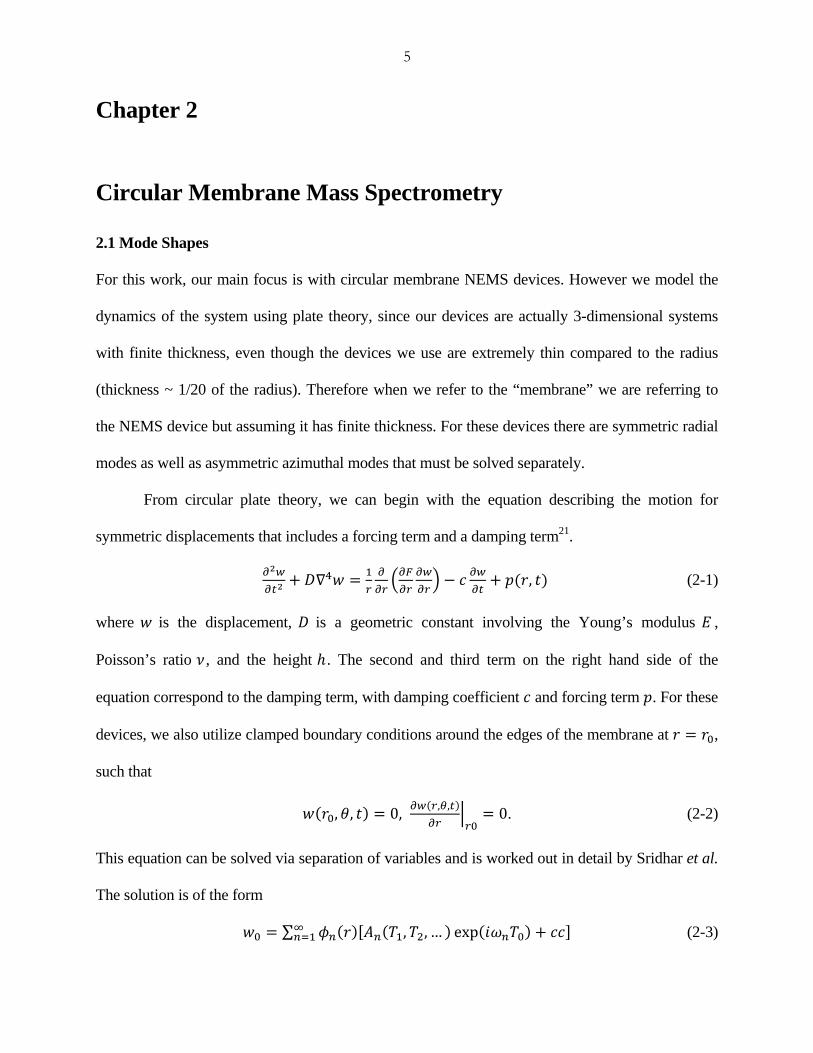
Chapter 2 Circular Membrane Mass Spectrometry
2.1 Mode Shapes
For this work, our main focus is with circular membrane NEMS devices. However we model the
dynamics of the system using plate theory, since our devices are actually 3-dimensional systems
with finite thickness, even though the devices we use are extremely thin compared to the radius
(thickness ~ 1/20 of the radius). Therefore when we refer to the “membrane” we are referring to
the NEMS device but assuming it has finite thickness. For these devices there are symmetric radial
modes as well as asymmetric azimuthal modes that must be solved separately.
From circular plate theory, we can begin with the equation describing the motion for
symmetric displacements that includes a forcing term and a damping term21.
𝜕2𝑤𝜕𝑡2
+ 𝐷∇4𝑤 = 1𝑟𝜕𝜕𝑟�𝜕𝐹𝜕𝑟
𝜕𝑤𝜕𝑟� − 𝑐 𝜕𝑤
𝜕𝑡+ 𝑝(𝑟, 𝑡) (2-1)
where 𝑤 is the displacement, 𝐷 is a geometric constant involving the Young’s modulus 𝐸 ,
Poisson’s ratio 𝜈 , and the height ℎ. The second and third term on the right hand side of the
equation correspond to the damping term, with damping coefficient 𝑐 and forcing term 𝑝. For these
devices, we also utilize clamped boundary conditions around the edges of the membrane at 𝑟 = 𝑟0,
such that
𝑤(𝑟0,𝜃, 𝑡) = 0, 𝜕𝑤(𝑟,𝜃,𝑡)𝜕𝑟
�𝑟0
= 0. (2-2)
This equation can be solved via separation of variables and is worked out in detail by Sridhar et al.
The solution is of the form
𝑤0 = ∑ 𝜙𝑛(𝑟)[𝐴𝑛(𝑇1,𝑇2, … ) exp(𝑖𝜔𝑛𝑇0) + 𝑐𝑐]∞𝑛=1 (2-3)

6
From this, the mode shapes for the symmetric modes have the form
𝜙𝑛(𝑟) = 𝑎𝑛[𝐽0(𝑘𝑛𝑟) + 𝜇𝑛𝐼0(𝑘𝑛𝑟)] (2-4)
where 𝐽0 is the Bessel function of the first kind and 𝐼0 is the modified Bessel function of the first
kind21. This is the primary equation we are interested in understanding. The constants are given by
𝜇𝑛 = − 𝐽0(𝑘𝑛)𝐼0(𝑘𝑛)
(2-5)
and 𝑎𝑛, the normalization constant, is defined such that the maximum value of 𝜙𝑛 is 1.
𝑀𝑎𝑥(𝜙𝑛) = 1 (2-6)
Furthermore, 𝑘𝑛 is found from the roots of the expression
𝐼0(𝑘𝑛)𝐽0′(𝑘𝑛) − 𝐼0′(𝑘𝑛)𝐽0(𝑘𝑛) (2-7)
Figure 2.1 shows the graph of the expression used to find the 𝑘𝑛 for the symmetric mode. The
values for 𝑘𝑛 are found in Table 2.1.
Figure 2.1: Plot of the expression 𝐼0(𝑘𝑛)𝐽0′(𝑘𝑛) − 𝐼0′(𝑘𝑛)𝐽0(𝑘𝑛) showing the first two roots for the symmetric modes, 01 and 02. The first two roots are 3.19622 and 6.30644.
1 2 3 4 5 6 7 x
15
10
5
5
10
15

7
Likewise the asymmetric case can be solved in a similar manner22. The mode shapes for the
asymmetric case have the form
𝜙𝑛𝑚(𝑟) = 𝑎𝑛𝑚[𝐽𝑛𝑚(𝑘𝑛𝑚𝑟) + 𝜇𝑛𝑚𝐼𝑛𝑚(𝑘𝑛𝑚𝑟)] (2-8)
Like the symmetric case, 𝑎𝑛𝑚 is the normalization constant and 𝜇𝑛𝑚 is defined in parallel fashion.
𝑘𝑛𝑚 are given by the roots of
𝐼𝑛(𝑘𝑛𝑚)𝐽𝑛′ (𝑘𝑛𝑚) − 𝐼𝑛′ (𝑘𝑛𝑚)𝐽𝑛(𝑘𝑛𝑚) (2-9)
A plot of this expression where 𝑛 = 1 is shown in Figure 2.2.
Figure 2.2: Plot of the expression 𝐼𝑛(𝑘𝑛𝑚)𝐽𝑛′ (𝑘𝑛𝑚) − 𝐼𝑛′ (𝑘𝑛𝑚)𝐽𝑛(𝑘𝑛𝑚) for the asymmetric modes, showing the first two roots corresponding to the 11 azimuthal modes and the 21 azimuthal modes.
The first root is 4.61090. For the first asymmetric mode, there will be two degenerate modes, which we call 11x and 11y. If
the circular plate is completely symmetric radially, then these two modes will have the exact same
frequency. This concept will be explored in further detail in Chapter 3.
From this, we can calculate the remaining parameters for the mode shapes. Table 2.1 shows
the values for the three constants for the first four modes. Figure 2.3 shows the mode shape as a
2 4 6 8 x
4
2
2
4

8
function of radius, with the maximum normalized to one. We also model the mode shapes using
finite element simulation.
Mode (m,n) 𝑎𝑚𝑛 𝜇𝑚𝑛 𝑘𝑚𝑛 01 Radial 0.94723 0.05571 3.19622
11x Azimuthal 1.65780 0.01522 4.61090 11y Azimuthal 1.65780 0.01522 4.61090
02 Radial 1.00253 -0.00253 6.30644
Figure 2.3: a) Plot of the 01 mode shape. b) Plot of 11 mode shape. c) Plot of 02 mode shape. d-g) Finite element simulations of the 01 mode, the two 11 degenerate modes, and the 02 mode.
Table 2.1: Parameters 𝑎𝑚𝑛 , 𝜇𝑚𝑛 , and 𝑘𝑚𝑛 for the first 4 modes. Note that 11x and 11y are degenerate modes and have the same parameters.
a)
c)
d) f) g) e) Max
0

9
The 01 radial mode is simply the up down mode with the antinode at the center of the device. The
11 degenerate modes have their nodal lines perpendicular to each other and passing through the
center of the device. Finally the 02 radial mode consists of two radial antinodes, one at the center
and one as a circular ring. We are also interested in the frequencies corresponding to these modes.
This will also be explained further in chapter 3.
2.2 Multimode Theory
In Chapter 1, we saw that the resonant frequency of the NEMS device will downshift as mass is
deposited onto the device. However we must also consider what is known as the effective mass of
the system, instead of the total mass, as in Eq. 1-3. The effective mass is a fraction of the total mass
and is used to account for the actual amplitude motion of the membrane. Utilizing total mass
assumes that every portion of the membrane is moving to the maximum amplitude, like a mass on
a spring system, however this is not the case in general for these resonators. To calculate the
effective mass we begin with the total geometric mass
𝑚𝑔𝑒𝑜 = 𝜌∭𝑟d𝑟d𝜃d𝑧 =𝜋𝑟02𝜌ℎ (2-10)
But now for the effective mass, we also need to integrate over the normalized mode shape.
𝑚𝑒𝑓𝑓 = 2𝜋𝜌ℎ ∫ 𝜙𝑛2𝑟d𝑟𝑟00 = 2𝑚𝑔𝑒𝑜
𝑟02∫ 𝜙𝑛2𝑟d𝑟𝑟00 (2-11)
The above equation only holds for the radial modes geometries, but can be generalized for any
geometry. We see that the effective mass is affected by the mode shape. Therefore the correction
factor for the effective mass is also dependent on the given resonant mode, as defined in the
previous section. Table 2.2 shows the values for the effective mass corrections for the first four
modes.

10
Replacing the mass from Eq. 1-3 with the effective mass, we have
𝛿𝜔0 = −12𝜔0
𝛿𝑚𝑒𝑓𝑓
𝑚𝑒𝑓𝑓 (2-12)
We also wish to represent the change in the effective mass in terms of the mass of the particle.
Depending where the particle lands on the device, its effective mass will similarly be scaled by the
mode shaped squared at that particular location
𝛿𝑚𝑒𝑓𝑓 = ∆𝑚𝑝𝑎𝑟𝑡𝑖𝑐𝑙𝑒𝜙02(𝑟𝑝,𝜃𝑝) (2-13)
Therefore we have, generalizing to any mode, 𝑛
𝛿𝜔𝑛 = −12𝜔𝑛
∆𝑚𝑝𝑎𝑟𝑡𝑖𝑐𝑙𝑒
𝑚𝑒𝑓𝑓𝜙𝑛2(𝑟, 𝜃) (2-14)
This shows that the frequency shift is dependent not only on the mass of the deposited particle, but
also on the amplitude of the particular mode where the particle landed10, 11. The above equation is
general for all geometries. For the specific case of circular membrane geometry, since the mode
shape has positional dependence in two dimensions, (𝑟,𝜃) or (𝑥,𝑦), we therefore have three
unknowns. This is the basis for multimode measurements; in order to decouple the particle mass
from its position, we require the measurement of three distinct, yet corresponding frequency shifts.
This in itself provides a series of experimental challenges that we will cover in the next few
chapters.
Due to the nature of mode shapes as combinations of Bessel functions, the solution can
only be found numerically and not analytically. The procedure for solving this system for the 01
and 11 modes is detailed below.
Mode Fractional Correction for Effective Mass 01 Radial 0.18283
11x Azimuthal 0.36918 11y Azimuthal 0.36918
02 Radial 0.10189
Table 2.2: Effective mass corrections for the 01, 11, 02 modes.

11
From Section 2.1, we add the two degenerate azimuthal modes in quadrature to eliminate
the angular dependence.
𝜙11𝑥2 + 𝜙11𝑦2 = 𝑎112 �𝐽1(𝑘11𝑟) + 𝜇11𝐼1(𝑘11𝑟)�2 sin2 𝜃 + 𝑎112 �𝐽1(𝑘11𝑟) + 𝜇11𝐼1(𝑘11𝑟)�2 cos2 𝜃
= 𝑎112 �𝐽1(𝑘11𝑟) + 𝜇11𝐼1(𝑘11𝑟)�2 (2-15)
From this, we can numerically solve for the radius by combining with Eq. 2-14 with Eq. 2-15. We
divide out the 2𝜋 from 𝜔, the angular frequency, to get 𝑓, the resonant frequency.
∆𝑓11𝑥𝑓11𝑥
+∆𝑓11𝑦𝑓11𝑦
∆𝑓01𝑓01
=𝜙11𝑥2 +𝜙11𝑦2
𝜙012 (2-16)
We then insert the radius back into Eq 2-14 and numerically solve for the particle mass.
∆𝑚𝑝𝑎𝑟𝑡𝑖𝑐𝑙𝑒 = −2 ∆𝑓01𝑓01
𝑚𝑒𝑓𝑓
𝜙012 (2-17)
As we can see, this method can only be performed numerically. Below we show modeling results
to confirm that this mathematical model is correct.
We first generate random positions on the disk with corresponding particles with random
masses. The range of particles is from 40 𝑛𝑚 gold nanoparticle (GNP) to 100 𝑛𝑚 GNP. The
dimensions for GNP refer to the diameter of these spherical particles. We then compute the
expected frequency shifts for the first three modes for the random particle at the randomized
position with Eq. 2-14. We take these frequencies shifts and following the above method, calculate
the radial position to back out the calculated mass. We compare these calculated and generated
mass and radii in Figure 2.4.

12
Figure 2.4: a) Plot of locations of N = 1000 simulated events. b) Plot of calculated radius versus actual generated radius. c) Plot of calculated particle mass versus actual generated particle mass.
For the generated locations, we see that we have all events within a circular device of normalized
radius 1, as expected. In Figure 2.4b, we plotted the calculated radius for each particle versus its
actual corresponding generated radius. We also differentiate for particles at 𝑟 > 0.8 , as the
calculation become less accurate. The blue lines indicate the 5% accuracy region from the actual
radius. In Figure 2.4c, we plot the calculated mass versus the actual mass for only particles at a
a) b)
c)

13
radius less than 0.8. Statistically, we obtain about 75% of these particles to remain within 5% of
the actual mass.
2.3 Allan Deviation
Another important consideration when performing NEMS MS is the potential mass resolution of
the system. In order to characterize the dynamic mass range, we must consider a quantity known as
the Allan deviation. The Allan deviation, 𝜎𝐴(𝜏), is a measure of the frequency stability of clocked
systems and can be used to estimate the signal stability that arises from noise processes and drift.
The Allan deviation is useful because it can be calculated for a range of integration times, 𝜏, so that
we can calculate the optimal measurement time to minimize the noise in a data sample10, 11.
The Allan deviation is simply defined as the square root of the Allan variance, 𝜎𝐴(𝜏)2.
𝜎𝐴(𝜏) = �𝜎𝐴(𝜏)2 (2-18)
The Allan variance is calculated by taking the difference of two fractional frequency changes. If
we have N total data points with a sampling time of 𝜏𝑠𝑎𝑚𝑝𝑙𝑒, we can bin the data into M subunits
corresponding to some time interval 𝜏 = 𝑎𝜏𝑠𝑎𝑚𝑝𝑙𝑒 , where 𝑎 is some integer corresponding to
𝑎 = 𝑁𝑀
. The Allan variance is then defined as
𝜎𝐴(𝜏)2 = 12(𝑀−1)
∑ (𝑦[𝑚 + 1] − 𝑦[𝑚])2𝑀𝑚=1 (2-19)
Where 𝑦[𝑚] is the average value of the mth bin. We see that the Allan variance is found by taking
the difference from adjacent data points rather than from the overall mean. This way we can
account for drifts over different time scales and long term drifts will not significantly affect the
variance in short time spans.
To measure and calculate the Allan deviation, we need to track the frequency of the system
over a long period of time to obtain sufficient data to measure both long term drifts and improve

14
the statistics. The exact experimental setup will be covered in Chapter 5, however suffice it to
understand now that the measurement simply involves frequency tracking over a period of time.
Since we will be utilizing a multimode measurement, it also becomes important to
understand the Allan deviation among all three modes. We measured the Allan deviation for all
three modes while actuating each mode independently. We also actuate all three modes
concurrently to determine if there are any correlation effects between the modes that would affect
that measurement. Figure 2.5 shows the Allan deviation for both individual and concurrent
actuation.
a)
b)
Figure 2.5: a) Plot of Allan deviation when each mode is actuated independently. b) Plot of Allan deviation when each mode is actuated concurrently.
a)
b)

15
For each measurement, we sample the resonant frequency every 500 𝑚𝑠. The data is then parsed
into different time intervals and the Allan deviation calculated for each integration time. The
upward slopping portion of the graph corresponding to short timescales corresponds to random
frequency noise, most likely due to thermomechanical noise and other noise processes. The
downward sloping portion is then dominated by the white noise regime and as we average longer,
the signal-to-noise begins to improve. The final turn and upward portion is due to long term drift.
After a certain time, long term drift begins to set in. The data then become noisy since we have
fewer points at longer integration times.
We see that the Allan deviation is not significantly affected by concurrent actuation of the
various modes. Since the mass sensitivity is proportional to the Allan deviation (described in the
next section), having consistent Allan deviation will help in maintaining consistent measurements.
2.4 Dynamic Mass Range
As we develop this model for NEMS-MS, it is important to estimate the potential dynamic mass
range to determine the effectiveness of the system. For the upper bound, we take the measureable
mass to be about 1/10 of the device’s effective mass. This arises from assuming that the deposited
particle is small compared to the overall device mass and can be treated as a point particle relative
to the device so that it does not significantly affect the mode shape. Additionally we make this
assumption since we only take up to the 1st order term of the Taylor series. Taking higher order
would allow us to relax his assumption slightly.
For the lower bound, we begin by approximating the frequency shift by the Allan
deviation, since the Allan deviation is a measure of the frequency stability.
∆𝑓𝑓0≈ 𝜎𝐴(𝜏) (2-20)
Furthermore assuming the particle lands at the antinode of the mode, we get

16
∆𝑚𝑝𝑎𝑟𝑡𝑖𝑐𝑙𝑒 ≈ 2𝑚𝑒𝑓𝑓𝜎𝐴(𝜏) (2-21)
Therefore we see that the lower bound for the dynamic range is dependent on two factors, the
effective mass of the device and the frequency stability of the system.
For these particular devices, the calculated geometric mass is about 18.3 𝑇𝐷𝑎 or about
3.03 × 10⁻¹⁴ 𝑘𝑔. This gives an effective mass for the first mode, based on the correction from
Table 2.2, of 3.35 𝑇𝐷𝑎 or about 5.57 × 10⁻¹⁵ 𝑘𝑔.
We also need to consider the frequency stability of the system. This is dictated by the noise
of the system and can arise from various sources including thermomechanical noise, electronic
noise, and photodetector noise. From above, we see that the minimal Allan deviation we can
achieve is 𝜎𝐴(τ) ≈ 10−6. Inserting this into Eq 2-21 we get a lower bound of the dynamic mass
range.
The total dynamic mass range is
6.7 𝑀𝐷𝑎 < ∆𝑚𝑝𝑎𝑟𝑡𝑖𝑐𝑙𝑒 < 180 𝐺𝐷𝑎 (2-22)
This gives us about a five order of magnitude range for the measureable mass.

17
Chapter 3: AlN Device Structure and Operation
3.1 AlN (Aluminum Nitride) Properties
As electromechanical devices attain smaller and smaller dimensions, it becomes important to
utilize materials with advantageous electronic properties. The development of more advanced
fabrication techniques has also opened the door for testing a wider variety of materials to
characterize and select the optimum device material. In particular, piezoelectric actuation for AlN
NEMS resonators seems to be a better choice13. The details and advantages of piezoelectricity for
AlN devices will be covered further in section 3.4.
AlN was first synthesized in the late 1800s, but its potential for electronic application was
not realized until the 1900s18. AlN is a semiconducting material that when processed into a thin
film, exhibits piezoelectric properties that make it advantageous for NEMS devices6, 23. Previous
work has shown that AlN devices have higher piezoelectric coupling efficiency compared to other
piezoelectric devices, such as gallium arsenide. AlN also has a high acoustic velocity and low
dielectric loss, which makes it a more suitable candidate for resonators13.
3.2 AlN Membrane Device Structure
For this particular experiment, we utilize AlN circular membranes. The devices consist of a stack
of alternating AlN and molybdenum (Mo). On top of the bulk silicon (Si) and silicon dioxide
(SiO2) substrate is a 50 𝑛𝑚 AlN layer (seed layer), a 40 𝑛𝑚 Mo layer, a 50 𝑛𝑚 AlN layer, and
finally a 40 𝑛𝑚 top Mo layer. This gives a total device thickness of 180 𝑛𝑚 . We have also
experimented with different thicknesses of devices. The purpose of the stack is to be able to apply
a voltage difference across the two Mo layers in order to piezoelectrically actuate the device.

18
The overall potential effective region of the device is about 8 µ𝑚 in diameter based on the
gold contacts patterned onto the surface, however the exact device dimension is unknown since the
released region is hidden below the surface. The top Mo layer also contains several important
fabrication features. The cuts across the top Mo layer dividing the surface into four quadrants and
exposing the top AlN layer acts as an aid to help induce the actuation of the degenerate modes. A
bridge cut is also made on one of the top Mo quadrants to further isolate the motion of that
quadrant to null out the background in certain measurement schemes. A hole is also created in the
center of the device and tunnels all the way through the piezoelectric layers to the base SiO2 layer.
This allows us to release the device via a wet etch, as hydrofluoric acid (HF) can etch away the
silicon dioxide layer.
The schematic in Figure 3.1a shows what the released underside of the device should
appear like, assuming a perfectly isotropic etch. From the scanning electron microscope (SEM)
images in Figure 3.1, we see both an overview of a set of devices (six total per pattern) and a
magnified image of one device. In the overview, the large polygon-shaped regions are the six gold
contacts for each device. The two horizontal contacts on either side are grounds connected to the
bottom Mo layer and the four other contacts correspond to the contacts on the four quadrants of the
device on the top Mo layer. In the zoomed in image, the darker area corresponds to the top Mo
layer and the lighter cut portions are the exposed top AlN layer. The medium gray shade is the
edge of gold contacts.

19
Figure 3.1: a) Schematic and dimensions of the piezoelectric stack. (Image not to scale) b) SEM images of the array of devices and magnified image of a single device.
The exact first mode frequency for a circular plate is given by the equation
𝜔2 = 40.7042𝐸ℎ2
12𝜌(1−𝜈2)𝑑4 (3-1)
where 𝐸 is the Young’s modulus, ℎ is the height of the plate, 𝜌 is the density, 𝜈 is the Poisson’s
ratio, and 𝑑 is the diameter. From this, if we assume a diameter of about 6 µ𝑚, we get a frequency
around 70 𝑀𝐻𝑧 which lines up with the measurements we describe in Chapter 4.
3.3 Overview of Fabrication Procedure
The fabrication of these devices is a multistep process following standard nanofabrication
procedures. We begin with prepared Si wafers containing the AlN stack. We then follow six step
of electron beam lithography. The first step is to write a mesa layer to etch away the top Mo and
top AlN layer from all regions except where the device will be located. We then write alignment
markers and evaporate gold onto them to act as guides during the remaining steps. The third write
is known as the cut layer and has two components, a high resolution cut and a course cut. The high
resolution write is to create the cross to isolate the four quadrants and bridge cut on the top Mo
layer of the device. The course cut is to electrically isolate the exposed bottom Mo layer in order to
create contacts. We then write the hole which goes all the way down to the oxide layer for HF
a) b)

20
etching. Then we write the isolation layer, which is used to evaporate strontium fluoride. This acts
as an isolation layer between the gold contacts and the bottom Mo layer, which is typically
grounded. Finally we write and evaporate the gold contact layer.
Once we are ready to use the device, we wet etch the device. We expect the HF etch to be
isotropic, so we expect a circular released device. We etch for 19 minutes, to obtain a device with
radius between 2 and 4 µ𝑚. The exact etch rate depends on the quality of the oxide and etch
solution.
3.4 Actuation Techniques
In order to measure the frequency of NEMS devices, we need to be able to actuate them to drive
the resonant modes. Throughout the NEMS community, there are several ways to actuate the
device, including capacitive, magnetomotive, and via piezoshakers. For these AlN devices, as
mentioned earlier, we choose to actuate these devices piezoelectrically due to better transduction
efficiency13.
Piezoelectricity is a property of materials that was first discovered in the 1880s. In general,
piezoelectricity refers to when a material is deformed mechanically, internally the structure
generates some sort of electric charge. This typically arises from when the applied stress causes a
change or reorientation of the dipoles in the material, altering the electric field in the material.
Conversely, piezoelectric materials, when applied an applied electric field, can react with
mechanical strain, deforming the material. In most cases, this piezoelectric property is reversible in
both the mechanical/electrical variations as well as the direction of the piezoelectric pathway. The
piezoelectric properties of the material are classified by the piezoelectric constants 𝑑𝑥𝑦 which
relate the strain to the polarization. In particular, AlN was found to have higher piezoelectric

21
coefficients, making it a more effective transducer of an applied electric field to mechanical
motion. Therein lies the advantage of utilizing AlN as a piezoelectrically actuated NEMS device.
To piezoelectrically actuate these AlN stack devices, we utilize the setup show in Figure
3.2. We apply an alternating current (AC) signal generated by the network analyzer (NA) to the top
Mo layer and ground the bottom Mo layer, creating an electric field in the vertical direction. This
induces the strain on the device that causes it to vibrate out of plane (up and down). Depending on
the AC frequency, we can drive the devices to resonance. For the multimode measurement for
mass spectrometry, we combine multiple driving signals that will actuate each individual mode.
Figure 3.2: Actuation scheme for these piezoelectric devices.
Au
22
3.5 Detection Schemes
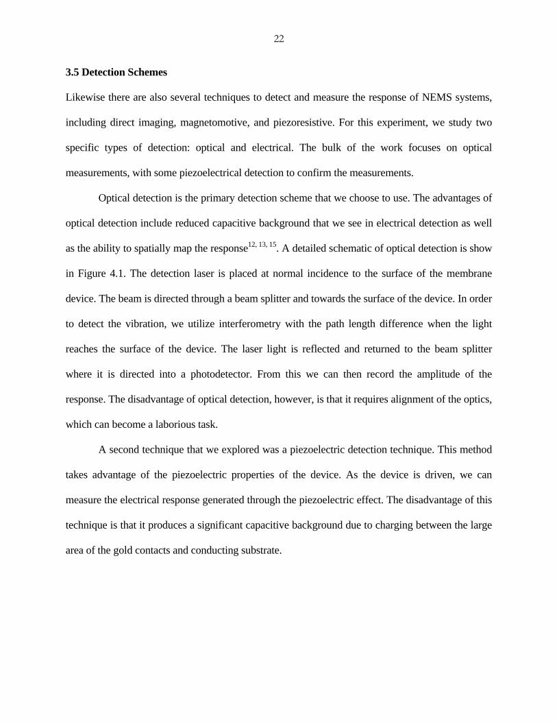
Likewise there are also several techniques to detect and measure the response of NEMS systems,
including direct imaging, magnetomotive, and piezoresistive. For this experiment, we study two
specific types of detection: optical and electrical. The bulk of the work focuses on optical
measurements, with some piezoelectrical detection to confirm the measurements.
Optical detection is the primary detection scheme that we choose to use. The advantages of
optical detection include reduced capacitive background that we see in electrical detection as well
as the ability to spatially map the response12, 13, 15. A detailed schematic of optical detection is show
in Figure 4.1. The detection laser is placed at normal incidence to the surface of the membrane
device. The beam is directed through a beam splitter and towards the surface of the device. In order
to detect the vibration, we utilize interferometry with the path length difference when the light
reaches the surface of the device. The laser light is reflected and returned to the beam splitter
where it is directed into a photodetector. From this we can then record the amplitude of the
response. The disadvantage of optical detection, however, is that it requires alignment of the optics,
which can become a laborious task.
A second technique that we explored was a piezoelectric detection technique. This method
takes advantage of the piezoelectric properties of the device. As the device is driven, we can
measure the electrical response generated through the piezoelectric effect. The disadvantage of this
technique is that it produces a significant capacitive background due to charging between the large
area of the gold contacts and conducting substrate.
23
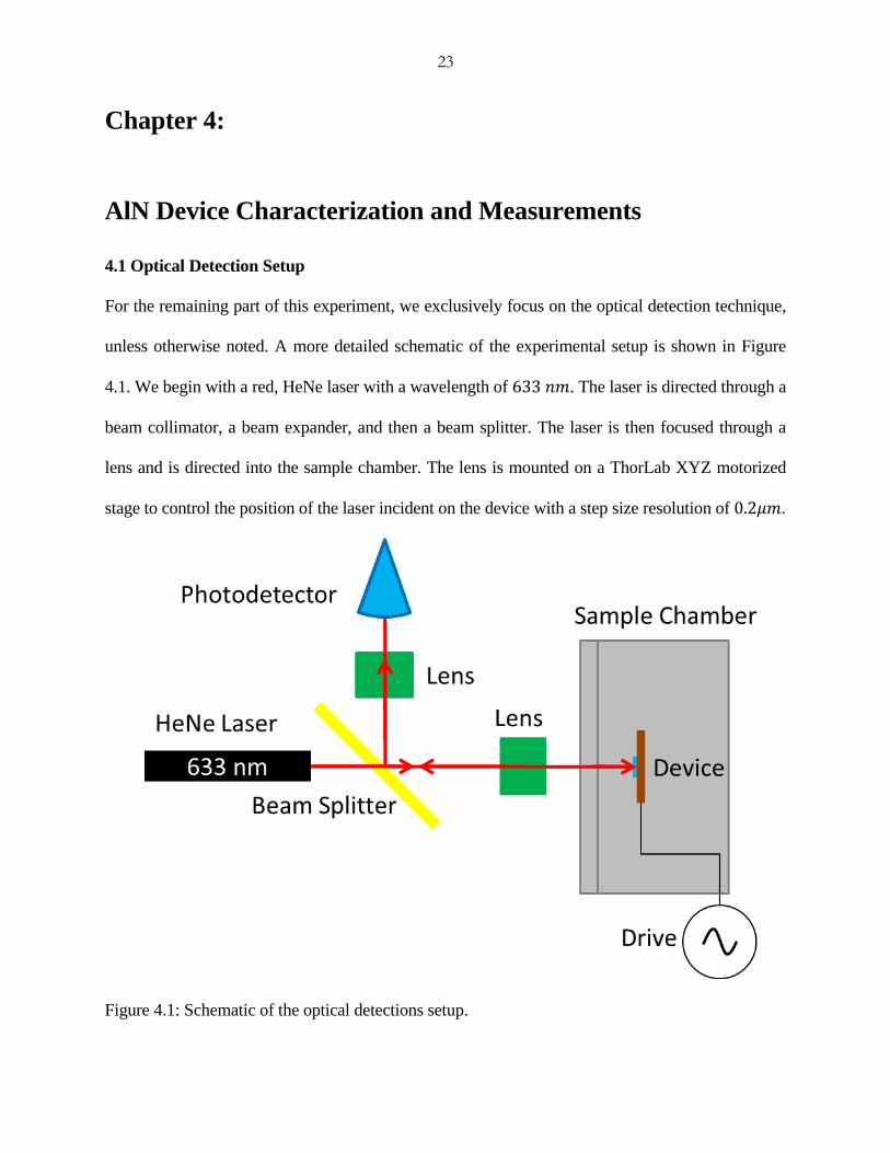
Chapter 4: AlN Device Characterization and Measurements
4.1 Optical Detection Setup
For the remaining part of this experiment, we exclusively focus on the optical detection technique,
unless otherwise noted. A more detailed schematic of the experimental setup is shown in Figure
4.1. We begin with a red, HeNe laser with a wavelength of 633 𝑛𝑚. The laser is directed through a
beam collimator, a beam expander, and then a beam splitter. The laser is then focused through a
lens and is directed into the sample chamber. The lens is mounted on a ThorLab XYZ motorized
stage to control the position of the laser incident on the device with a step size resolution of 0.2𝜇𝑚.
Figure 4.1: Schematic of the optical detections setup.

24
The sample chamber is an approximately 6” diameter aluminum cylinder with modifications for
optical detection, a vacuum connection, and electrical connections. On the front side, a 2” round
opening is fitted with a quartz window to allow the optical detection laser to enter. The side of the
chamber contains an opening to connect vacuum components to pump down the chamber and the
back panel contains eight electrical SMA outputs. Internally, the chamber contains an elevated,
adjustable stage to mount the chip carrier. The chip carrier is a ceramic holder that contains gold
contacts that pass through the ceramic to electrical readout pins. A typical chip carrier that we use
contains 64 possible pins. To connect the device to the chip carrier, we wire bond the contacts on
the chip carrier to the contacts on the device. We can then map the device electrodes to the pin
readouts. Figure 4.2 shows a more detailed image of the chamber and sample carrier.
Figure 4.2: a) Image of the inside of the sample chamber. b) Image of the back panel of the sample chamber with the electrical connections. c) Schematic of the inside of the sample chamber showing the laser paths and chip carrier.
a)
b)
c)

25
After the optical detection laser enters the chamber, it is reflected off the device and returns
to the beam splitter and is then directed into the photodetector. The interference pattern arises from
the path length difference between either the device surface and the substrate or the device surface
and the quartz window. From this, we can readout the responsitivity of the device. The electrical
readout of the photodetector is connected to the input channel of a network analyzer.
4.2 Spatial Response Scan
After loading the device into the chamber and pumping down the system to about 10−5 𝑡𝑜𝑟𝑟, we
can manually focus the laser onto the device by following the projected image on a piece of paper.
Utilizing the NA, we sweep over a wide range of frequencies to identify the resonant peaks. We
focus on the lowest frequency peak which we expect to correspond to the 01 radial mode. We
manually sweep in the X, Y, and Z direction of the motors to optimize the position of the laser on
the device and the amplitude of the signal. We define X, Y to be in the plane of the device and Z to
be the focus direction of the lens. We are looking for the very center of the device because we
expect the amplitude of the response to be maximal there since that is the location of the antinode
of the first mode.
Following our manual rough optimization, we can perform a more systematic 3D XYZ
scan of the laser position to finely optimize its position, especially in the focal plane. This is done
iteratively by first stepping through each X position for a given Y and Z position, then moving to
the next Y position and repeating the step through of the X direction. After completing a set of Y
scans, the program takes the next step in the Z direction and repeats the scan of the XY plane. The
XYZ motorized stage is controlled through LabView via a Universal Serial Bus (USB) connection.
At each position, the NA takes a frequency sweep of the selected frequency span via a General
Purpose Interface Bus (GPIB) between the NA and computer. After each sweep, the program picks
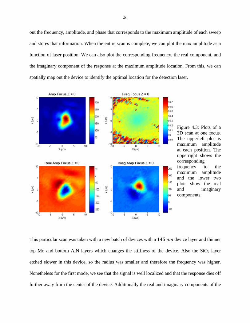
26
out the frequency, amplitude, and phase that corresponds to the maximum amplitude of each sweep
and stores that information. When the entire scan is complete, we can plot the max amplitude as a
function of laser position. We can also plot the corresponding frequency, the real component, and
the imaginary component of the response at the maximum amplitude location. From this, we can
spatially map out the device to identify the optimal location for the detection laser.
Figure 4.3: Plots of a 3D scan at one focus. The upperleft plot is maximum amplitude at each position. The upperright shows the corresponding frequency to the maximum amplitude and the lower two plots show the real and imaginary components.
This particular scan was taken with a new batch of devices with a 145 𝑛𝑚 device layer and thinner
top Mo and bottom AlN layers which changes the stiffness of the device. Also the SiO2 layer
etched slower in this device, so the radius was smaller and therefore the frequency was higher.
Nonetheless for the first mode, we see that the signal is well localized and that the response dies off
further away from the center of the device. Additionally the real and imaginary components of the
27
signal have the expected shape. For this particular device, we see a fundamental mode at about
94.2 𝑀𝐻𝑧. For the frequency plot in the upper right, we see a central blue patch that corresponds
to about 94.2 𝑀𝐻𝑧, however as we move radially away from the center, we see that the frequency
increases. This may be due to some heating effects from the laser, where the center of the device is
heated and the material is slightly softer, which would lower the true resonant frequency. This
difference is about 1% of the total resonant frequency.
Another consideration is the convolution of the laser spot size with the size of the device.
The spot size of the laser is about 5µ𝑚, so this is comparable to the size of the device. Therefore
there is some convolution with the exact readout, which is why the effective device area seems
slightly larger than in reality. From finite element simulations of these devices, the corresponding
radius for a 94.2 𝑀𝐻𝑧 device is about 2.3 𝜇𝑚. Similarly for the first generation of devices that
have the thicker 180 𝑛𝑚 stack dimensions as described in section 3.2, the frequency of 70 𝑀𝐻𝑧
corresponds to a device size of about 2.8 𝜇𝑚.
We perform the same scan for the higher order modes as well, mapping out the device
when driven at the 11 azimuthal modes. The plots are shown below in Figure 4.4.
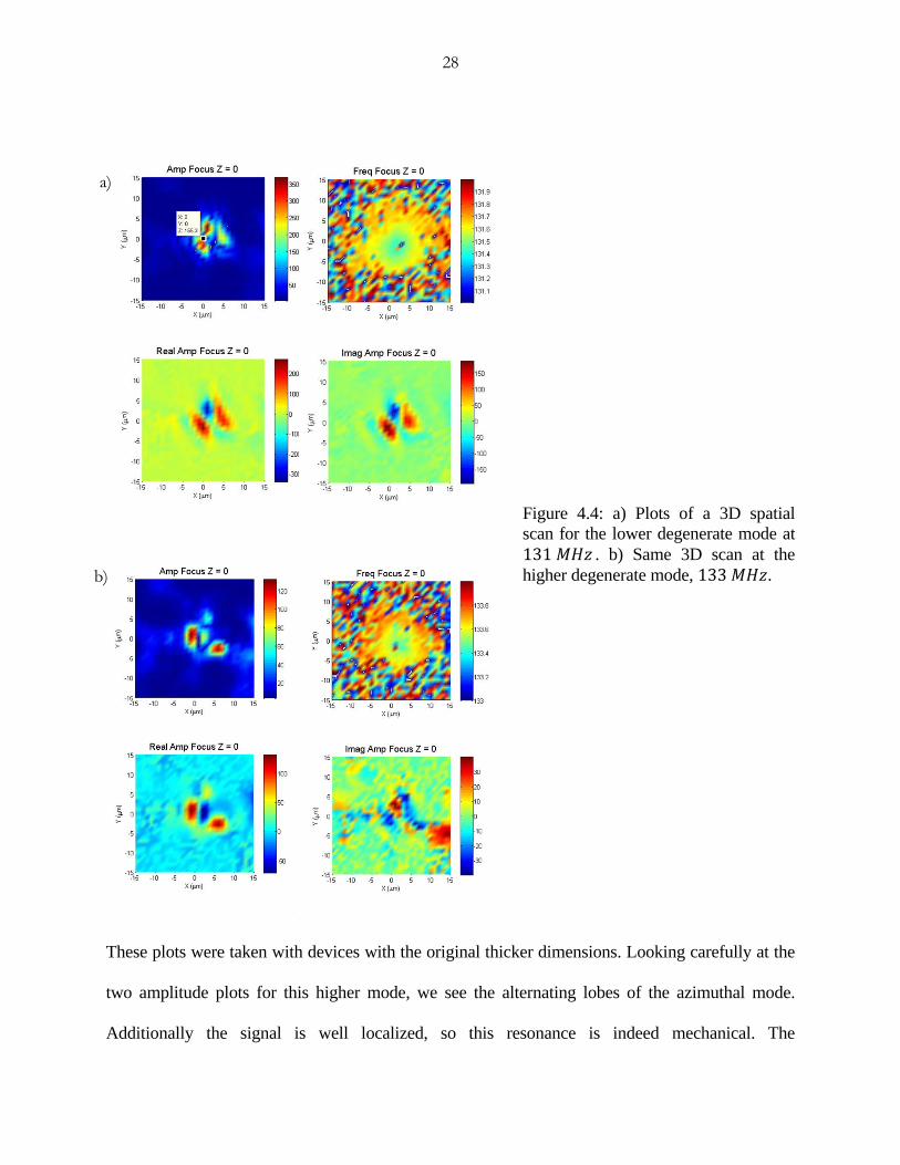
28
Figure 4.4: a) Plots of a 3D spatial scan for the lower degenerate mode at 131 𝑀𝐻𝑧 . b) Same 3D scan at the higher degenerate mode, 133 𝑀𝐻𝑧.
These plots were taken with devices with the original thicker dimensions. Looking carefully at the
two amplitude plots for this higher mode, we see the alternating lobes of the azimuthal mode.
Additionally the signal is well localized, so this resonance is indeed mechanical. The
b)
a)
29
corresponding frequencies are about 131 𝑀𝐻𝑧 and 133 𝑀𝐻𝑧 . The cause of this frequency
splitting will be detailed in the next section. These frequencies match up well with the predicted
frequencies from theory and finite element simulations. Also, there is potential to attempt to release
the devices for a longer period of time to increase the radius and lower the frequency. This will be
useful to allow measurement of even higher modes. Currently we are limited to a maximum
frequency of 200 𝑀𝐻𝑧 by the measurements equipment.
Comparing the positions of all three modes, we need to select a laser position that
optimizes the response of all three modes. For example, selecting the maximum for the 01 mode
theoretically corresponds to the nodal lines for the degenerate modes, so in practice we want to
offset the laser position slightly. Furthermore, the transduction efficiency of the higher modes is
lower since we require more energy to actuate them. Therefore we choose a location that can
provide the greatest response for the higher modes. The 01 mode typically has a much higher
signal-to-noise ratio, so we can move off the antinode of the first mode while still maintaining a
high signal-to-noise ratio.
4.3 Frequency Sweeps
The next step is to characterize the responsivity of the device because it is important to understand
the physics of the device to effectively use it for mass spectrometry. This is done by performing
more specific frequency sweeps with the network analyzer by applying different drives to the
device and by averaging each sweep for a longer period of time. We expect that as we increase the
voltage applied to the device, the amplitude of the response will increase. At a certain point, the
response will become nonlinear. Amplitude sweeps of the first mode is shown in Figure 4.5.

30
69.4 69.6 69.8 70.0 70.2 70.40.0
0.2
0.4
0.6
0.8
1.0
1.2
1.4
1.6
1.8Am
plitu
de (m
V)
Frequency (MHz)
Amplitude
-100
-50
0
50
100
Phase (deg)
Phase
69.6 69.8 70.0 70.2 70.4 70.6
0
50
100
150
200
250
Ampl
itude
(µV)
Frequency (MHz)
800mV 600mV 400mV 200mV
Figure 4.5: a) Amplitude and phase for the resonance. b) Plot of ampltiude resopnse as a function of frequency for different drive voltages. c) Plot of frequency sweep in the up and down direction showing the hystersis due to nonlinearity.
66.0 66.2 66.4 66.6 66.8 67.0 67.2
0
5
10
15
20
25
30
35
40
Ampl
itdue
(µV)
Frequency (MHz)
up sweep down sweep
Each of the above plots was taken from different devices, but from the same batch of devices. The
central frequencies are all slightly different due to the uncertainty from the radius of the device
during the releasing process of fabrication. Additionally the amplitude response of each device is
slightly different due to fabrication variations that can affect the efficiency. This is one major
challenge as we attempt to scale up the system to arrays of devices. We have measured first mode
resonances with amplitudes as low at 10’s of 𝜇𝑉 to as high as 1 𝑚𝑉. The 𝑄 factor for the first
mode is approximately 650.
As we see from Figure 4.5a the phase goes through an 180° phase shift as it passes through
the resonance. In Figures 4.5b, we see the nonlinear response of the devices. This is characterized
a) b)
c)

31
by the increasing resonant frequency as well as the sudden sharp drop off in amplitude. For
resonances in general, nonlinearity can arise from a variety of sources, including fabrication
defects, natural damping, and the measurement scheme. For these devices, we believe that the
nonlinearity is geometric and arises when we drive the device beyond their linear limits; that is
where the amplitude of its motion is far greater than its thickness. This geometric effect leads to a
positive Duffing term, which results in a higher resonant frequency17. We also see the hysteresis
depending on the direction that the frequency is swept, further indicating the nonlinear response.
The nonlinearity further confirms that we are looking at a real, mechanical resonance from the
device.
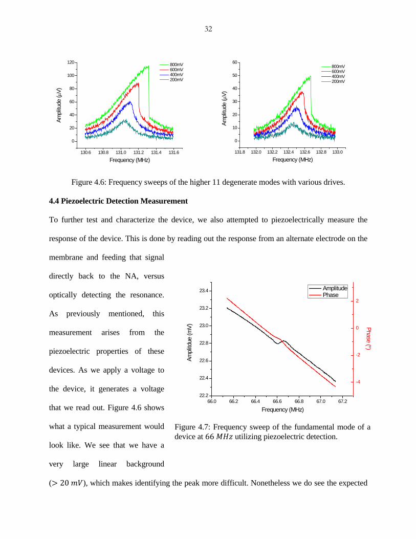
We also sweep the frequency of the higher 11 degenerate modes. We see that the
supposedly degenerate modes have a frequency splitting of about 1.5 𝑀𝐻𝑧 between the two
modes. Across the different devices we have measured, we have seen frequency splitting anywhere
from being almost perfect degeneracy to 2 𝑀𝐻𝑧. This frequency splitting is caused by asymmetry
during the fabrication process that breaks these modes. For example the alignment of the cross cuts
in the top Mo layer may not be perfectly symmetric or the HF release was not perfectly isotropic.
This characteristic is actually very useful for mass spectrometry because we can utilize these two
modes as part of our measurement, rather than looking for higher order modes. For the device
scanned in Figure 4.6, we see resonant frequencies for the degenerate modes at about 131 𝑀𝐻𝑧
and 132.5 𝑀𝐻𝑧. For these higher modes, we have been able to see amplitudes between 10’s of 𝜇𝑉
up to 100’s 𝜇𝑉. The overall transduction efficiency of these modes is lower since these modes are
much more difficult to actuate compared to the fundamental mode, hence why we include the cuts.
For the linear resonances, we get a 𝑄 of about 750. Again we see that we can achieve non-linearity
when we increase the drive amplitude.
32
130.6 130.8 131.0 131.2 131.4 131.6
0
20
40
60
80
100
120Am
plitu
de (µ
V)
Frequency (MHz)
800mV 600mV 400mV 200mV
131.8 132.0 132.2 132.4 132.6 132.8 133.0
0
10
20
30
40
50
60
Ampl
itude
(µV)
Frequency (MHz)
800mV 600mV 400mV 200mV
Figure 4.6: Frequency sweeps of the higher 11 degenerate modes with various drives.
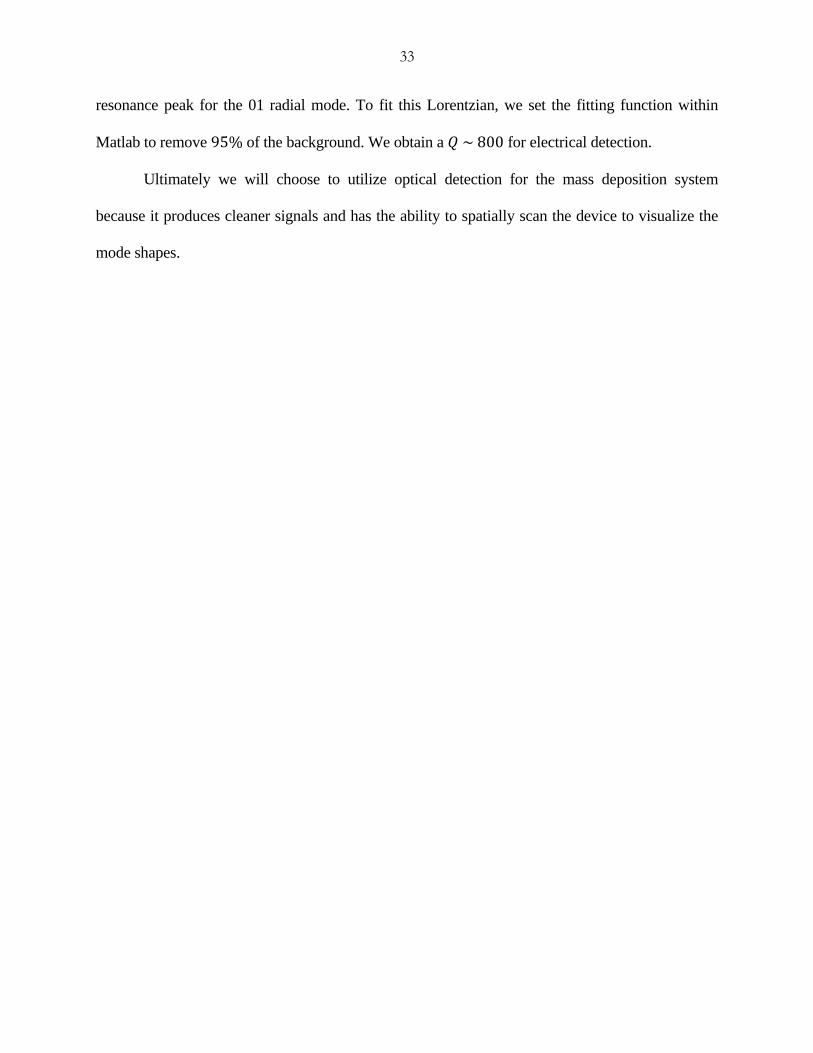
4.4 Piezoelectric Detection Measurement
To further test and characterize the device, we also attempted to piezoelectrically measure the
response of the device. This is done by reading out the response from an alternate electrode on the
membrane and feeding that signal
directly back to the NA, versus
optically detecting the resonance.
As previously mentioned, this
measurement arises from the
piezoelectric properties of these
devices. As we apply a voltage to
the device, it generates a voltage
that we read out. Figure 4.6 shows
what a typical measurement would
look like. We see that we have a
very large linear background
(> 20 𝑚𝑉), which makes identifying the peak more difficult. Nonetheless we do see the expected
66.0 66.2 66.4 66.6 66.8 67.0 67.222.2
22.4
22.6
22.8
23.0
23.2
23.4
Ampl
itdue
(mV)
Frequency (MHz)
Amplitude Phase
-4
-2
0
2
Phase (°)
Figure 4.7: Frequency sweep of the fundamental mode of a device at 66 𝑀𝐻𝑧 utilizing piezoelectric detection.
33
resonance peak for the 01 radial mode. To fit this Lorentzian, we set the fitting function within
Matlab to remove 95% of the background. We obtain a 𝑄 ~ 800 for electrical detection.
Ultimately we will choose to utilize optical detection for the mass deposition system
because it produces cleaner signals and has the ability to spatially scan the device to visualize the
mode shapes.

34
35
Chapter 5: Mass Spectrometry Experimental Setup
5.1 Optical Detection/Mass Deposition Setup
After the devices are characterized, we can attempt to mass load. To do this, we modify the typical
detection setup to be able to incorporate the mass deposition portion of the experiment. The first
adjustment is to offset the quartz window so that we can accommodate both the detection laser,
which will be centered with respect to the aluminum cover, and the UV laser for mass deposition,
which will be incident at an angle to the device. Therefore the window itself is not centered with
respect to the chamber, but rather offset towards the right based on the orientation of our setup. On
the inside surface of the front cover containing the quartz window, we place an angled bracket used
to mount mass sample slides. The detailed schematic of the chamber is shown in Figure 4.2. The
UV laser is aligned so that it is normal to this sample slide, but positioned such that the deposition
process will have flux directed towards the device. The UV laser is a pulsed 355 𝑛𝑚 beam that is
focused through a second lens that can be controlled with its own XYZ motorized stage. The pulse
rate is triggered with a function generator set to a pulse waveform. A schematic and picture of the
aggregate setup is shown in Figure 5.1.
The mass deposition technique we use is known as MALDI. Since we are initially testing
GNPs, we can utilize this soft ionization technique. MALDI involves an energy transfer when the
UV laser is pulsed onto the back of the sample. The matrix that the analyte is embedded in absorbs
the UV energy and transfers it to the particle. The energized particle are then desorbed off the
sample into the sample chamber and towards the device.
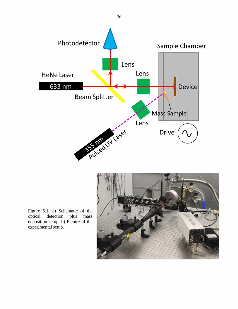
36
Figure 5.1: a) Schematic of the optical detection plus mass deposition setup. b) Picutre of the experimental setup.
37
5.2 Phase-locked Loop Setup
In order to track the frequency of all three modes in real time while attempting to mass load the
device, we utilize a phase-locked loop (PLL) measurement setup. In general, a PLL is a technique
that takes in two signals, a test frequency and a reference frequency, and compares the two phases.
Based on the phase difference, a voltage controlled oscillator (VCO) outputs a signal with a phase
relative to the phase of the reference. This type of circuit is useful when the frequencies change and
the PLL can adjust the frequency by looking at the relative phase of the two systems. Hence we see
the usefulness of such a setup to track frequency shifts from mass deposition events14.
For our PLL experimental setup, we utilize a set of three SRS844 high frequency lock-in
amplifiers and three function generators to take measurements. For each mode, we feed a drive
signal from the function generator into both the device and the reference input for the lock-in
amplifier. For the first mode, we utilize an Agilent 33250a waveform generator since the frequency
is below 80 𝑀𝐻𝑧. This particular function generator has a built in reference output so we do not
need to split its output. For the two higher modes we utilize HP8648 function generators since they
can output higher frequencies, up to several gigahertz. These HP8648 function generators do not
contain reference outputs, therefore the output signal is split via a power splitter and fed into the
corresponding lock-in amplifier’s reference input. For each mode, the input signal from each
function generator is combined with the other two modes by using a power splitter as a combiner
and then connected to an electrode on the device. The output signal from the photodetector is split
into the input of each respective lock-in. The lock-ins and function generator are controlled via
GPIB from a LabView program. A diagram of the experimental measurement setup is shown in
Figure 5.2. The PLL measurement continuously tracks the frequency and continuously corrects the
drive frequency to account for any shifts in resonance, such as from a mass loading event. The

38
advantage of using this technique, versus continuous frequency sweep with a network analyzer is
that we can rapidly record data by only picking out the resonance frequency based on the phase.
Additionally this allows faster switching between measuring each mode, rather than waiting for an
entire frequency sweep to finish.
Figure 5.2: Schematic of the PLL setup for three modes. The blue power splitters are where they are used as power combiners.
Additionally we can adjust several parameters of the PLL system to improve our measurements.
The first parameter is the timing of the system, which is characterized by two values, the lock-in
time constant, 𝜏𝐿𝐼, and the sampling time, 𝑇𝑠𝑎𝑚𝑝𝑙𝑒. The sampling time in general is taken to be
about five times the lock-in time constant. 𝜏𝐿𝐼 refers to the filter within the lock-in. Generally
increasing this value will reduce the noise, but only up to a certain point as long term drifts will
begin to set in. We also can adjust the filter value on the lock-in. Typically we choose a filter of 12
dB/octave. Within the LabView software, we can adjust the Y to 𝜙 conversion, a digital filter. This
39
is how fast or slow the PLL will adjust the frequency to shifts in the phase. Between all these
parameters, we want to be able to minimize the noise processes in the system as well as maintain
an efficient tracking time. Additionally, we want to optimize these parameters for the PLL loop
time, explained below.
When a mass loading event occurs and the frequency downshifts, the entire time it takes
from event to measurement by the system is known as the PLL loop time. Our goal is to match this
loop time to the integration time corresponding to the minimum of the Allan deviation, as
described in Section 2.3 to obtain the lowest mass sensitivity. Typically we first pick a 𝜏𝐿𝐼 that
minimizes the Allan deviation at the desired loop time. Then we adjust the Y to 𝜙 conversion such
that a measurement will take about 20 data points from the occurrence of mass loading to reading
the entire frequency jump.
5.3 Mass Sample Preparation
For the first generation of experiments, we utilized
40 𝑛𝑚 gold nanoparticles. These have a mass of
6.47 × 10⁻¹⁹ 𝑘𝑔 or 389 𝑀𝐷𝑎. To prepare the sample
slides to mount into the chamber, we need to
concentrate and dry the GNP sample. The GNP is
purchased from Sigma-Aldrich as a colloidal
suspension in a buffered salt solution. The first step is
to perform a buffer exchange to replace the salt
solution with deionized water (DI water). Our goal is to reduce the salt concentration by a factor of
1000. The purpose of this buffer exchange is to prevent any unwanted species from mass loading
during the deposition process. To accomplish this, we spin down about 5 𝑚𝐿 of GNP solution in a
Figure 5.3: Picture of the sample slide where the GNP is deposited in a grid.

40
centrifuge to about 250 𝜇𝐿, then add in DI water back to 5 𝑚𝐿 and repeat several more times to
wash out more salt each time. After this, we concentrate the GNP down to about 500 µ𝐿. Each of
these centrifuge steps is done at 4500 𝑟𝑝𝑚. This is enough material to create two slides.
The next step is to pipette the GNP onto a 1" square glass sample slide and then allow it to
dry. To facilitate drying, we heat the sample slide at 80°𝐶 on a hot plate. Other techniques to speed
up the drying process include vacuum drying or replacing the DI water with a solvent, such as
isopropyl alcohol. The purpose of accelerating the drying is both to reduce the sample prep time as
well as counteract what is known as the “coffee ring effect” which arises when droplets of solution
are dried4. Figure 5.3 shows what a typical sample slide looks like. We notice that the edge of each
dot is darker than the interior. This is due to the capillary flow that cause GNP to clump towards
the edges of the liquid as it dries. The GNP solution can either be pipetted onto the sample slide in
a grid like fashion or randomly. However after each layer, we must wait for it to dry before
pipetting the next layer on. To be able to get sufficient covering, we typically pipette about ten
layers.
From experimenting with the different procedures, heating the sample slide is the most
efficient and most stable method of pipetting the GNP. Also, pipetting the GNP in a random
fashion is easier for the desorption laser to produce an event because the particles are not
concentrated in localized areas.
5.4 Mass Deposition Experiments
During the first test of the combined mass deposition/optical detection system, we only utilized one
mode tracking to ensure that the system functions correctly. While we run the PLL frequency
tracking on one mode, we scan and pulse the UV laser at a rate comparable to the PLL time.

41
60000 62000 64000 66000 68000 7000072.450
72.453
72.455
72.457
72.460
72.463
72.465
Freq
uenc
y (M
Hz)
Time (sec)
62880 62890 62900 62910 62920 62930
72.456
72.457
72.458
72.459
72.460
72.461
72.462
Freq
uenc
y (M
Hz)
Time (sec)
Figure 5.4: a) Data from first test run of setup tracking the first resonant mode. b) Zoomed in plot of the first frequency jump.
From the first test run, we see that we were able to resolve a few jumps. From 5.4b. we see that the
PLL loop response time is about 5 seconds for the 5.5 𝑘𝐻𝑧 jump. This loop time and frequency
shift seem reasonable. If we assume that the particle landed at the center (𝜙01 = 1,𝜙11𝑥 = 𝜙11𝑦 =
0), then we have an estimated mass corresponding to the mass of two 40 𝑛𝑚 particles. However
this is just an order of magnitude estimate to test the entire set up.
To confirm that we were able to successfully deposit GNP onto the device, we perform
several experimental checks. The first check is simply to image the device for the presence of GNP
under an SEM. A before and after image of the device is shown in Figure 5.5. On the left we see a
fairly clean device, however in the right side image, we see distinct bright round spots. We believe
that this corresponds to GNP due to the roundness and brightness of the particles.
a) b)

42
Figure 5.5: Before (left) and after (right) images of an AlN device under GNP mass deposition.
To confirm this, we perform energy dispersive x-ray spectroscopy (EDX) on both the device and
these bright particles. EDX is a spectroscopy tool used to identify elements in a sample by focusing
a beam of x-rays onto the sample. These x-rays then excite electrons in the sample into higher
energy states. The excited electron can now either decay back into the ground state, releasing
energy in the process, or can be ejected and another higher energy electron falls into the grounds
state. In either case energy is released and this difference can be measured. Since each element has
unique energy levels, we can identify the corresponding elements present in the sample.
Figure 5.6 shows the spectrum obtained for both the background and a particle. The black
spectrum corresponds of the control measurement by focusing the x-ray beam on the surface of the
device where there does not appear to be any GNP present. As expected, we can identify peaks at
about 0.5 𝑘𝑒𝑉, 1.5 𝑘𝑒𝑉, 1.7 𝑘𝑒𝑉, and 2.3 𝑘𝑒𝑉. These correspond to oxygen, aluminum, silicon,
and molybdenum, respectively. This is our expected background since all these elements are
present within the device. When we focus the electron beam on a region with the GNP, we
measure an extra peak at an energy of about 2.1 𝑘𝑒𝑉, which corresponds to the 𝑀𝛼 energy level of
gold. This confirms the identity of the GNP. Table 5.1 summarizes these values.

43
0.0 0.5 1.0 1.5 2.0 2.5 3.0
0.0
0.2
0.4
0.6
0.8
1.0
1.2
1.4In
tens
ity (A
.U.)
X-ray Energy (keV)
Background GNP
Figure 5.6: EDX of the device with and without GNP deposition.
Table 5.1: Summary of energy levels in O, Al, Si, Mo, and Au
Element Energy (𝑘𝑒𝑉) Level Oxygen (O) 0.523 𝐾𝛼
Aluminum (Al) 1.486 𝐾𝛼 Silicon (Si) 1.740 𝐾𝛼
Molybdenum (Mo) 2.293 𝐿𝛼 Gold (Au) 2.120 𝑀𝛼
From this we can now attempt to mass load while tracking three resonant modes. This is done with
the same experimental setup, but with the full PLL structure described in Section 5.2. We also
increase the GNP size to 80 𝑛𝑚. This is in order attempt to improve the visibility of the frequency
shifts across all modes, since certain frequency shifts could be hidden within the frequency noise.
Data from this run is shown in Figure 5.7. We tracked the frequency for an extremely long
period of time while rastering the UV laser over the GNP mass sample. We notice a distinct long
term frequency shift of about 20 − 30 𝑘𝐻𝑧 for each mode from a time of about 10000 seconds to
20000 seconds, however we were unable to resolve individual frequency jumps. We believe this
large frequency shifts corresponds to multiple particles being deposited, but too rapidly for our
PLL detection scheme to resolve. When a particle lands on the device, the PLL will begin
44
adjusting the measured frequency, however while the PLL is still adjusting, another particle is
deposited and further shifts the frequency. This causes the data to be mixed between particle
events. In addition, several other runs gave us similar results, where we see regions of large
frequency shifts, however the flux rate was again too fast for us to resolve the shifts.
Figure 5.7: Frequency tracking data for the first three modes during mass deposition of 80 𝑛𝑚
GNP.
Nonetheless, from this round of experiments, we were able to show that we can track the frequency
shifts across all three modes and that we can mass deposit with our current setup.
45
From these scans, we were also able to back calculate the positions of the UV laser that
corresponded to the downward frequency shift region. This would allow us to narrow down the
scanning region of the UV laser to make the scan more efficient and allow us to scan the laser with
finer resolution. By performing PLL scans with the order of X and Y motors swapped, we were
able to identify a ¼” by ¼” region of the slide that seemed to correspond to the optimal location for
mass deposition. Future experiments will most likely focus on this region of the slide. This also
allows us to save GNP solution by creating the sample slide with material only in this region.

46

47
Chapter 6: Conclusion
In conclusion, we have worked out the mathematical model for 2-dimensional mass spectrometry
with NEMS circular membrane devices. From the simulations we see that the calculations should
work. In addition we showed the improved capability of optical detection for this type of
measurement by eliminating the background capacitive noise. Previous work within the group has
shown that optical detection is advantageous for graphene measurements, so this experimental
setup opens the door for mass spectrometry with graphene devices. We were also able to record
preliminary data showing the ability for this setup to deposit particle onto the device as well as the
ability for it to track up to three frequency modes of the device. Our preliminary data and
investigation showed initial signs of mass deposition, however our flux rate and mass resolution
needs to be improved.
For further work, we are interested in optimizing the setup. In particular we wish to
improve the flux rate of the system. This can be done by better controlling the position of the laser
or the rate of pulsing. Additionally we wish to improve the Allan deviation in order to improve the
measurement. Also as briefly mentioned earlier, we wish to try out graphene devices for mass
spectrometry due to their low device mass. We are also looking to measure higher modes to
expand our multimode measurement to track four or five frequencies to improve our resolution.

48

49
Bibliography 1. Andersson, C-O. “Mass Spectrometric Studies on Amino Acid and Peptide Derivatives”. Acta
Chemica Scandivanica. 1958 12 1353.
2. Beynon, J.H. “The Use of the Mass Spectrometer for the Indentification of Organic
Compounds”. Microchimica Acta. 1956 44 437-453.
3. Bunch, J.S, et al. “Electromechanical Resonators from Graphene Sheets”. Science. 2007 315
490-493.
4. Deegan, R.D, et al. “Capillary Flow as the Cause of Ring Stains from Dried Liquid Drops”.
Nature. 1997 389 827-829.
5. Deutsch, B.M, et al. “Non-degenerate Normal-mode Doublets in Vibrating Flat Circular
Plates”. American Journal of Physics. 2004 72(2) 220-.
6. Dubois. M, P. Muralt. “Properties of Aluminum Nitride Thin Films for Piezoelectric
Transducers and Microwave Filter Applications”. Applied Physics Letters. 1999 74 3032.
7. Ekinci, K.L, M.L. Roukes. “Nanoelectromechanical Systems”. Review of Scientific
Instruments. 2005 16 061101.
8. Ekinci, K.L, Y.T. Yang, M.L. Roukes. “Ultimate Limits to Inertial Mass Sensing Based Upon
Nanoelectromechanical Systems”. Journal of Applied Physics. 2004 95 5.
9. Ekinci, K.L. “Electromechanical Transducers at the Nanoscale: Actuation and Sensing of
Motion in Nanoelectromechanical Systems (NEMS)”. Small. 2005 1 786-797.
10. Hanay, M.S. Towards Single-Molecule Nanomechanical Mass Spectrometry. PhD thesis,
California Institute of Technology. 2011.

50
11. Hanay, M.S, et al. “Single-Protein Nanomechanical Mass Spectrometry in Real Time”. Nature
Nanotechnololgy. 2012.
12. Karabacek, D.M, et al. “Diffraction of Evanescent Waves and Nanomechanical Displacement
Detection”. Optics Letters. 2007 32(13) 1881-1883.
13. Karabalin, R.B, et al. “Piezoelectric Nanoelectromechanical Resonators Based on Aluminum
Nitride Thin Films”. Applied Physics Letters. 2009 95 103111.
14. Kharrat, C, E. Colinet, A, Voda. “H∞ Loop Shaping Control for PLL-based Mechanical
Resonance Tracking in NEMS Resonant Mass Sensors”. IEEE Sensors. 2008 1135-1138
15. Kouh, T, et al. “Diffraction Effects in Optical Interferometric Displacement Detection in
Nanoelectromechanical Systems”. Applied Physics Letters. 2005 86 013106.
16. Li, M, et al. “Ultra-sensitive NEMS-based Cantilevers for Sensing, Scanned Probe and Very
High-frequency Applications”. Nature Nanotechnology. 2007 2 114-120.
17. Lifshitz, R, M.C. Cross. “Nonlinear Dynamics of Nanomechanical and Micromechanical
Resonators”. Review of Nonlinear Dynamics and Complexity. 2008.
18. Mallet, J.W. “On Aluminum Nitride, and the Action of Metallic Aluminum Upon Sodium
Carbonate at High Temperature”. 1876.
19. Naik, A.K, et al. “Towards Single-molecule Nanomechanical Mass Spectrometry”. Nature
Nanotechnology. 2009 4 445-450.
20. Peng, W, et al. “Laser-Induced Acoustic Desorption Mass Spectrometry of Single
Bioparticles”. Angewandte Chemie. 2006 45 1423-1426.
21. Sridhar, S, D.T. Mook, A.H. Nayfeh. “Non-Linear Resonances in the Forced Responses of
Plates, Part I: Symmetric Responses of Circular Plates” Journal of Sound and Vibration. 1975
41(3), 359-373.
51
22. Sridhar, S, D.T. Mook, A.H. Nayfeh. “Non-Linear Resonances in the Forced Responses of
Plates, Part II: Asymmetric Responses of Circular Plates” Journal of Sound and Vibration.
1978 59(2), 159-170.
23. Taylor, K.M, C. Lenie. “Some Properties of Aluminum Nitride”. Journal of Electrochemical
Society. 1960 107(4) 308-314.
24. Yang, Y.T, et al. “Zeptogram-scale Nanomechanical Mass Sensing”. Nano Letters. 2006 6
583-586.
25. Young, D.J, C.A. Zorma, M. Mehregany. “MEMS/NEMS Devices and Applications”.
Springer Handbook of Nanotechnology. 2004 225-252.