dry etching - university of minnesota 07 dry etching_full.pdfdry etching advantages ... rie =...
TRANSCRIPT
Dry Etching
Prof. Tianhong Cui, Mechanical Engineering
ME 8254

Dry Etching Overview What is dry etching?
– Material removal reactions occur in the gas phase.
Types of dry etching– Non-plasma based dry etching
– Plasma based dry etching
Why dry etching?
Development of dry etching
Plasma parameters/influences
Deep Reactive Ion Etching

Dry Etching Advantages Eliminates handling of dangerous acids and solvents
Uses small amounts of chemicals
Isotropic or anisotropic etch profiles
Directional etching without using the crystal orientation of Si
Faithfully transfer lithographically defined photoresist patternsinto underlying layers
High resolution and cleanliness
Less undercutting
No unintentional prolongation of etching
Better process control
Ease of automation (e.g., cassette loading)

Dry Etching Disadvantages:
– Some gases are quite toxic and corrosive
– Re-deposition of non-volatile compounds
– Need for specialized (expensive) equipment
Types:– Non-plasma based = uses spontaneous reaction
of appropriate reactive gas mixture
– Plasma based = uses radio frequency (RF)power to drive chemical reaction

Non-plasma Based DryEtching
Isotropic etching of Si
Typically fluorine-containing gases(fluorides or interhalogens) that readily etchSi
High selectivity to masking layers
No need for plasma processing equipment
Highly controllable via temperature andpartial pressure of reactants

Xenon Difluoride (XeF2)Etching
Isotropic etching of Si
High selectivity for Al, SiO2, Si3N4, PR,PSG
2XeF2 + Si 2Xe + SiF4
Typical etch rates of 1 to 3 m/min
Heat is generated during exothermicreaction
XeF2 reacts with water (or vapor) to formHF
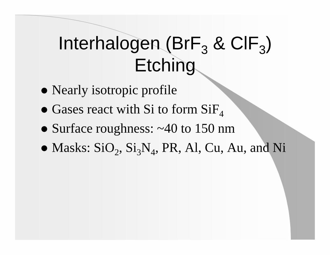
Interhalogen (BrF3 & ClF3)Etching
Nearly isotropic profile
Gases react with Si to form SiF4
Surface roughness: ~40 to 150 nm
Masks: SiO2, Si3N4, PR, Al, Cu, Au, and Ni

Plasma Based Dry Etching RF power is used to drive chemical
reactions
Plasma takes place of elevated temperaturesor very reactive chemicals
Types:– Physical etching
– Chemical etching
– Reactive ion etching (RIE)
– Deep reactive ion etching (DRIE)

Plasma Plasma = partially ionized gas consisting of equal
numbers of “+” (ions) and “-“ (electrons) charges anda different number of neutral (un-ionized) molecules
An ion-electron pair is continuously created byionization and destroyed by recombination
Typical kinetic energy (KE) of an electron in plasma is2-8 eV
KE = ½ mV2 = 3/2 kT– m = particle mass– V = particle mean velocity– k = Boltzmann constant– T = temperature (K)
2 eV electron hasT 15,000 KV 6 x 107 cm/s= 1,342,16176 mph

Plasma Formation Chamber is evacuated
Chamber is filled with gas(es)
RF energy is applied to a pair of electrodes
Applied energy accelerates electronsincreasing kinetic energy
Electrons collide with neutral gasmolecules, forming ions and more electrons
Steady state is reached (plasma); ionization= recombination

Plasma Formation Plasma discharge is characterized by central glow
or bulk region and dark or sheath regions nearelectrodes
Bulk region = semi-neutral (nearly equal numberof electrons and ions)
Sheath regions = nearly all of the potential drop;accelerates “+” ions from bulk region whichbombard the substrate
Maintained at 1 Pa (75 mtorr) to 750 Pa (56 torr)with gas density of 27 x 1014 to 2 x 10¹⁷
molecules/cm3

Plasma Parameters Temperature
– Etching rate
– Spontaneous chemicalreaction
– Etching directivity
Pressure– Ion density
– Ion directivity
Power– Ion density
– Ion kinetic energy
Other variables– Gas flow rate
– Reactor materials
– Reactor cleanliness
– Loading(microloading)
– Mask materials

Physical Etching (SputterEtching)
Based on physical bombardment with ions or atoms
Plasma is used to energize a chemically inert projectile sothat it moves at high velocity when it strikes the substrate
Momentum is transferred during the collision
Substrate atoms are dislodged if projectile energy exceedsbonding energy
Very similar to ion implantation, but low-energy ions areused to avoid implantation damage
Highly anisotropic
Etch rates for most materials are comparable (ie, nomasking)
Argon is the most commonly used ion source
May result in re-deposition

Two Basic Plasma Systems

Chemical (Plasma) Etching: Plasma is used to produce chemically reactive
species (atoms, radicals, and ions) from inertmolecular gas
Six major steps:– Generation of reactive species (eg, free radicals)– Diffusion to surface– Adsorption on surface– Chemical reaction– Desorption of by-products– Diffusion into bulk gas
Production of gaseous by-products is extremelyimportant

Plasma Etching Steps

Plasma Etching Systems Plasma Etching
(PE)
Barrel, barrel withdownstream andsymmetricalparallel platesystem
Pure chemicaletching
Isotropic etching

Reactive Ion Etching (RIE) RIE = process in which chemical etching is
accompanied by ionic bombardment (ie ion-assisted etching)
Bombardment opens areas for reactions
Ionic bombardment:– No undercutting since side-walls are not
exposed
– Greatly increased etch rate
– Structural degradation
– Lower selectivity

RIE System Reactive Ion Etching (RIE) Asymmetrical parallelplate system
Plasma, sheath andboundary layer
Combination of physicaland chemical etching
Anisotropic etching

Disadvantages of RIE Conflict between etching rate and anisotropic
profile
– Etching rate (+) Reactive speciesconcentration (+) Gas pressure (+)Collision (+) Anisotropic (-)
Conflict between damage of high etchingrate and anisotropic profile
– KE (+) Etching rate (+) damage (+)
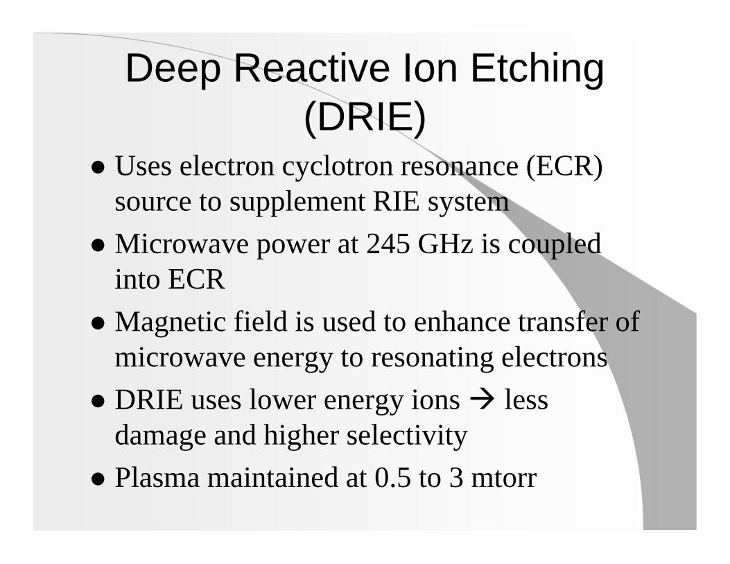
Deep Reactive Ion Etching(DRIE)
Uses electron cyclotron resonance (ECR)source to supplement RIE system
Microwave power at 245 GHz is coupledinto ECR
Magnetic field is used to enhance transfer ofmicrowave energy to resonating electrons
DRIE uses lower energy ions lessdamage and higher selectivity
Plasma maintained at 0.5 to 3 mtorr

ECR Systems Electron Cyclotron
Resonance (ECR) Higher plasma density
at lower pressure Control the density of
the reactive ions andtheir kinetic energyseparately
Downstream of plasmafurther limits theexposure to reducedamage

ICP System (DRIE)
Inductively CoupledPlasma (ICP)
Simple system
Almost same processresult as that from theECR system
Two RF powergenerators to controlion energy and iondensity separately

• high density ICP plasma• high aspect ratio Si structures• cost: $500K• vendors: STS, Alcatel, PlasmaTherm
Source: LucasNova
Source: AMMISource: STS Source: STS
Deep Reactive Ion Etching

Etch Chemistries
Organic Films– Oxygen plasma is required
– By-products: CO, CO2, H2O
– Masks: SiO2, Al, or Ti
– Addition of fluorine containing gasessignificantly increases etch rate but decreasesselectivity (due to HF formation)
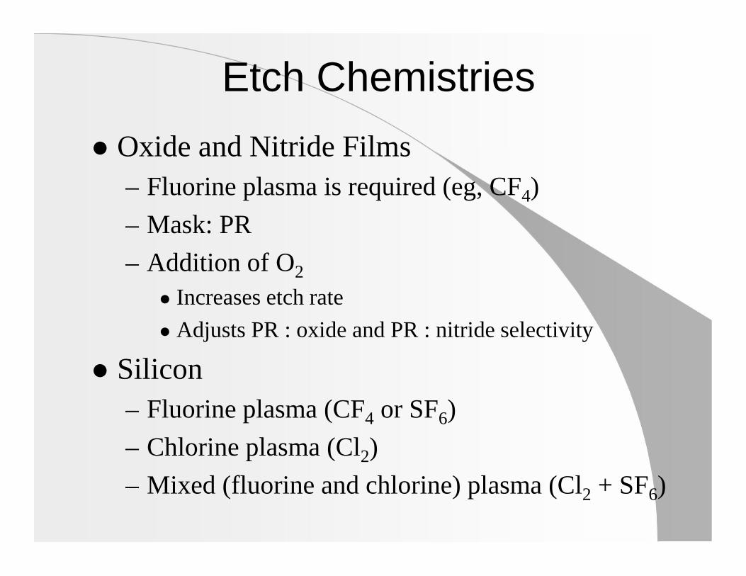
Etch Chemistries Oxide and Nitride Films
– Fluorine plasma is required (eg, CF4)
– Mask: PR
– Addition of O2
Increases etch rate
Adjusts PR : oxide and PR : nitride selectivity
Silicon– Fluorine plasma (CF4 or SF6)
– Chlorine plasma (Cl2)
– Mixed (fluorine and chlorine) plasma (Cl2 + SF6)

1-High Etch Rate
Process-ICP (ALCATEL)
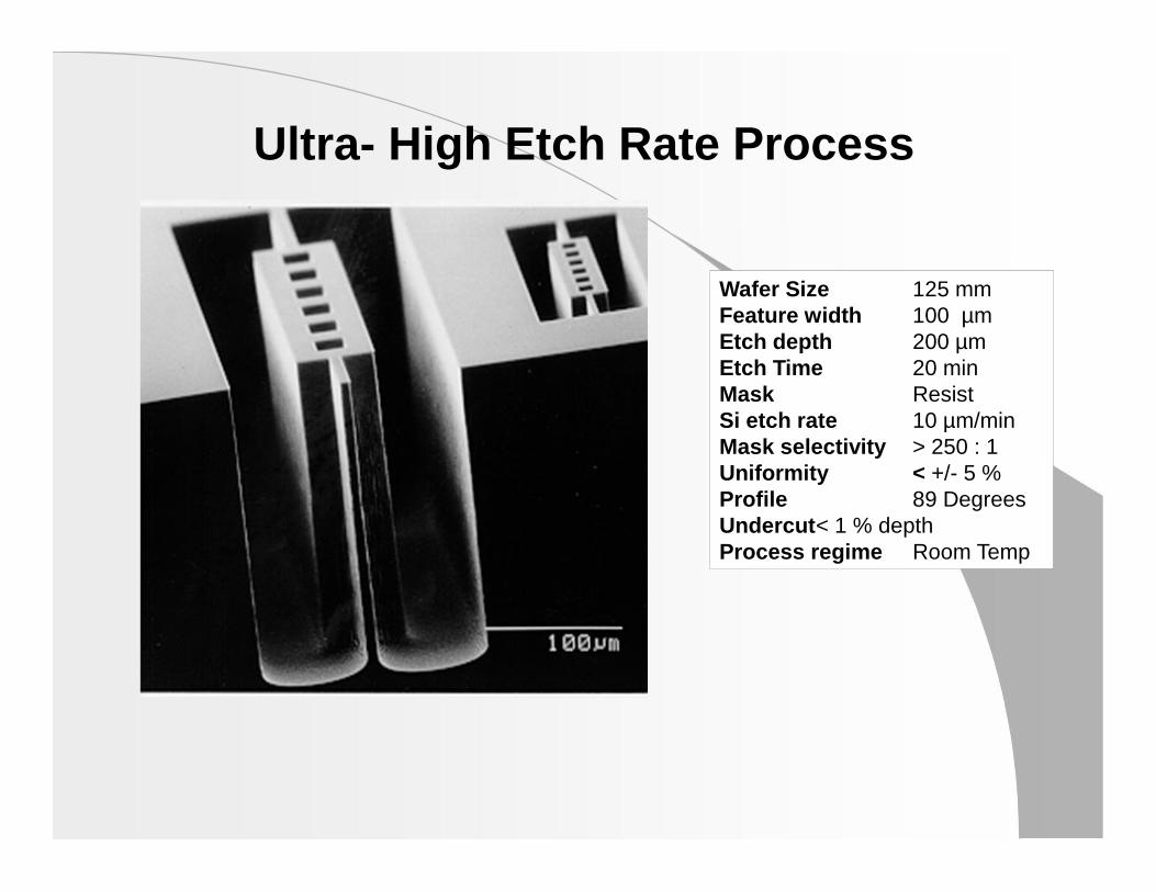
Wafer Size 125 mmFeature width 100 µmEtch depth 200 µmEtch Time 20 minMask ResistSi etch rate 10 µm/minMask selectivity > 250 : 1Uniformity < +/- 5 %Profile 89 DegreesUndercut< 1 % depthProcess regime Room Temp
Ultra- High Etch Rate Process

Ultra- High Etch Rate Process
Wafer Size 125 mmEtch depth 200 µmEtch Time 20 minMask ResistSi etch rate 10 µm/minMask selectivity > 250 : 1Uniformity < +/- 5 %Profile 89 DegreesUndercut< 1 % depthProcess regime Room Temp
2-High Aspect Ratio
Process-ICP

High Aspect RatioWafer diameter 100 mmFeature width 3.5 µmEtch depth 85 µmEtch time 30 minMask OxideSi etch rate 2.8 µm/minMask selectivity > 200 : 1Uniformity < +/- 5 %Profile 89 DegreesUndercut0.3 µmProcess regime Room Temp
Wide beam 1 µmEtch depth 90 µmSi etch rate 1.6 µm/minAspect ratio 90 : 1
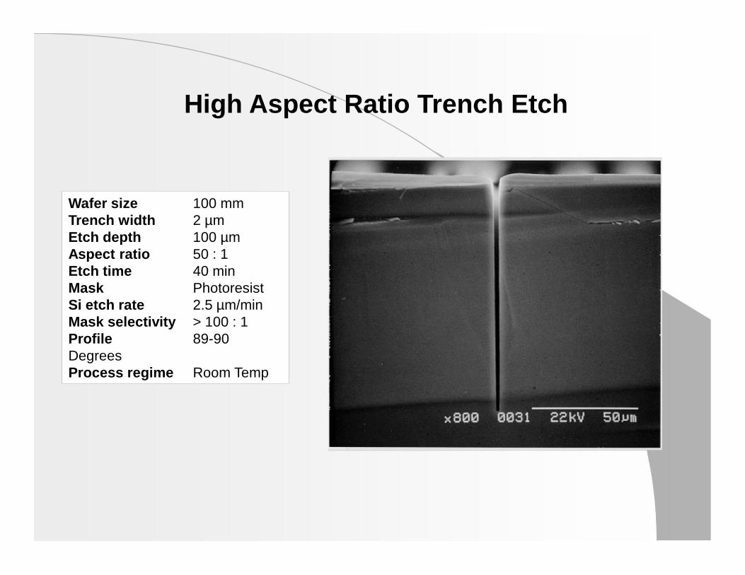
Wafer size 100 mmTrench width 2 µmEtch depth 100 µmAspect ratio 50 : 1Etch time 40 minMask PhotoresistSi etch rate 2.5 µm/minMask selectivity > 100 : 1Profile 89-90DegreesProcess regime Room Temp
High Aspect Ratio Trench Etch
3-Through the Wafer
Process-ICP

Wafer size 100 mmEtch depth 400 µmMask OxideSi etch rate 3.7 µm/minMask selectivity > 400 : 1Profile 90+/- 2DegreesProcess regime Low temp
Micro-Gears as Micro-Mechanical Components

Courtesy : Case Western Reserve University
Bulk Micromachined Spring(Through-the-wafer etch)
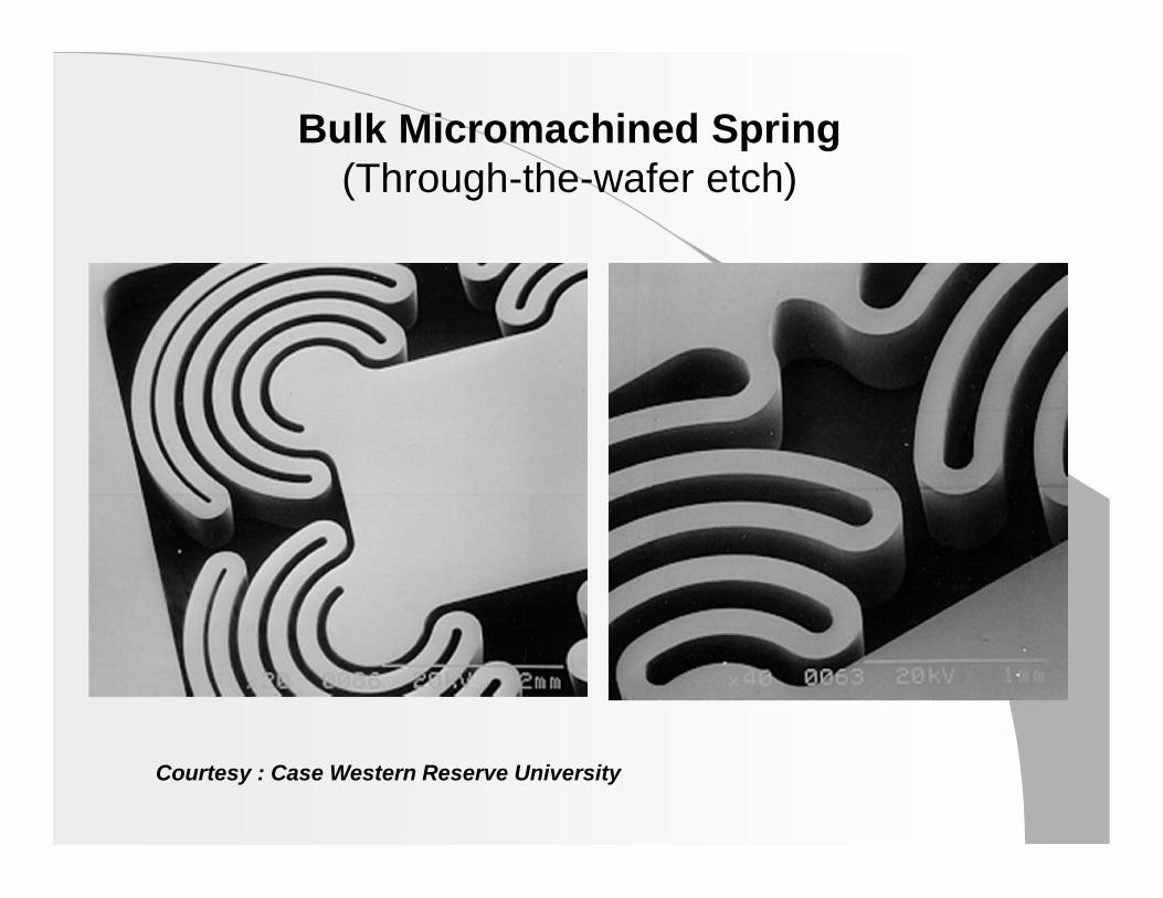
Courtesy : Case Western Reserve University
Bulk Micromachined Spring(Through-the-wafer etch)

4-VariousSOITaperedIsotropic Etch
Process-ICP

1.2 mm & >30 mm wide trenches
6 mm thick Si etch stoppingon buried oxide20 % overetch
Wafer Size 125 mmEtch Time 20 minMask ResistSi etch rate 3 µm/minMask selectivity > 100 : 1Uniformity < +/- 5 %Profile 90 DegreesProcess regime Room Temp
SOI etch with different feature sizes

20 µm deep
50 µm deep
30 µm deep
40 µm deep
Feature width 2 µmEtch depth 20-50 µmMask ResistSi etch rate 3.5 µm/minMask selectivity > 100 : 1Profile 87-89DegreesUndercut< 0.2 µmProcess regime Room Temp
Tapered profiles for SOI Trench Isolation
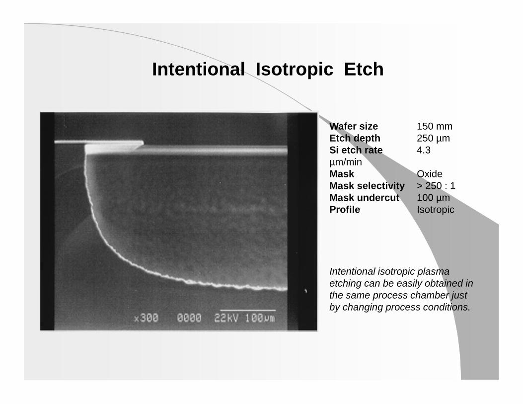
Wafer size 150 mmEtch depth 250 µmSi etch rate 4.3µm/minMask OxideMask selectivity > 250 : 1Mask undercut 100 µmProfile Isotropic
Intentional isotropic plasmaetching can be easily obtained inthe same process chamber justby changing process conditions.
Intentional Isotropic Etch

Problems and Solutions Trench Area Dependent Etching of Profiles Bowing RIE lag Micro grass Bottling Tilting

Some Real Pictures