pcl-240ak user's manual - nippon pulse · - 1 - 1. general description the pcl-240ak is the...
TRANSCRIPT


CONTENTS
1. GENERAL DESCRIPTION ................................................................................................................................................................................................................................................................................................................................................................1111
2. SPECIFICATIONS ....................................................................................................................................................................................................................................................................................................................................................................................................................2222
2-1 MAJOR SPECIFICATIONS .......................................................................................... 2 2-2 B1OCK DIAGRAM...................................................................................................... 3 2-3 PIN ASSIGNMENT & DIMENSIONS ........................................................................... 4 2-4 ELECTRICAL CHARACTERISTICS .............................................................................. 5
2-4-1 Absolute Maximum Ratings ................................................................................. 5 2222----4444----2 Recommended Operating Conditions2 Recommended Operating Conditions2 Recommended Operating Conditions2 Recommended Operating Conditions............................................................. 5 2222----4444----3 DC Characteristics (under recommended conditions)3 DC Characteristics (under recommended conditions)3 DC Characteristics (under recommended conditions)3 DC Characteristics (under recommended conditions) .................................. 5 2222----4444----4 AC Characteristics4 AC Characteristics4 AC Characteristics4 AC Characteristics........................................................................................... 6
3. INPUT/OUTPUT SIGNALS ................................................................................................................................................................................................................................................................................................................................................................8888
3-1 SIGNAL FUNCTIONS ................................................................................................. 8 3-2 PINS VS. SIGNALS .................................................................................................. 11
4.CNTENTS OF READ & 4.CNTENTS OF READ & 4.CNTENTS OF READ & 4.CNTENTS OF READ & WRITE DATAWRITE DATAWRITE DATAWRITE DATA............................................................................................................................................................................................................................................................................12121212
5. COMMANDS5. COMMANDS5. COMMANDS5. COMMANDS ........................................................................................................................................................................................................................................................................................................................................................................................................................................13131313
5-1 OUTLINE OF COMMANDS ....................................................................................... 13 5-2 START-STOP COMMAND ......................................................................................... 14 5-3 OPERATION MODE SELECT COMMAND.................................................................. 15 5-4 REGISTER SELECT COMMAND ............................................................................... 16 5-5 OUTPUT MODE SELECT COMMAND ....................................................................... 18
6. REGISTERS6. REGISTERS6. REGISTERS6. REGISTERS ............................................................................................................................................................................................................................................................................................................................................................................................................................................20202020
6-1 R0: 24-BIT DOWN COUNTER .................................................................................. 20 6-2 R1: 13-BIT FL REGISTER........................................................................................ 21 6-3 R2: 13-BIT FH1 REGISTER...................................................................................... 21 6-4 R3: 13-BIT FH2 REGISTER...................................................................................... 21 6-5 R4: 14-BIT ACCELERATION RATE REGISTER.......................................................... 22 6-6 R5: 14-BIT DECELERATION RATE REGISTER ......................................................... 22 6-7 R6: 20-BIT RAMPING-DOWN POINT REGISTER ...................................................... 22 6-8 R7: 16-BIT MULTIPLICATION REGISTER ................................................................ 23 6-9 R10: 24-BIT CURRENT POSITION COUNTER .......................................................... 24 6-10 R11: 13-BIT CURRENT FREQUENCY MONITOR .................................................... 24 6-11 R12: 24-BIT EXTENSION MODE REGISTER L ....................................................... 24 6-12 R13: 16-BIT EXTENSION MODE REGISTER 2 ....................................................... 30 6-13 R16: 24-BIT COMMAND BUFFER MONITOR ......................................................... 32 6-14 R17: 8-BIT EXTENSION STATUS BUFFER ............................................................. 32
7. STATUS READ7. STATUS READ7. STATUS READ7. STATUS READ............................................................................................................................................................................................................................................................................................................................................................................................................................33333333
8. TIMING CHARTS8. TIMING CHARTS8. TIMING CHARTS8. TIMING CHARTS ........................................................................................................................................................................................................................................................................................................................................................................................................34343434

- 1 -
1. General Description
The PCL-240AK is the CMOS LSI which can generate pulses at a maximum speed of 240 kpps. Its design features include an automatic ramping down point setting function, current position counter, phase distribution circuit and an interface to a servomotor, thereby making it suitable to controlling of stepping motors and ,servomotors.
The basic operation modes include the standard mode which lets the PCL-240AK perform to the specifications of the PCL-240K, and the extension mode which lets it outperform the PCL-240K. A desired mode is selectable through a software technique. Under the default condition initiated by resetting, the PCL-240AK is placed in the standard mode and can replace the PCL-240K.
Major Features Single 5V power supply low current consumption Automatic ramping-down point setting function Current position counter Phase distribution circuit for 4-phase/5-phase stepping motors 24-bit latch buffer for the interface to CPU Replace ability for PCL-240K 40-pin, plastic dip (600 mils)

- 2 -
2. Specifications
2-1 Major Specifications
Power Requirement: ・・・・・・・・・・・・・・・・・・ 5V ±5 % Reference Clock:・ ・・・・・・・・・・・・・・・・・・・・・ 4.9152MHz (standard) Pulse Rate Setting Range: ・・・・・・・・・・・・・・ 1 to 16777215 Pulse Rate Setting Steps: ・・・・・・・・・・・・・・・ 8191 Pulse Rate Multiplication:・・・・・・・・・・・・・・ 0.01 to 30 Typica1Output Pulse Rate Range: ・・・・・・ 1x mode: 1 to 8191 pps
10x mode: 30 to 245730 pps Pulse Rate Setting Registers: ・・・・・・・・・・・ 3 types of FL, FH1 and FH2 Ramping-down Point Setting Range:・・・・ 1 to 1048575 Acceleration Setting Range: ・・・・・・・・・・・・ 2 to 16383 Deceleration Setting Range: ・・・・・・・・・・・・ 2 to 16383 Current Position Counting Units: ・・・・・・・ 1 to 16 pulses/count Current Position Counter:・・・・・・・・・・・・・・ 24-bit up/down counter
(0 to 16777215) or (-8388608 to +8388607)
Representative Operations Available:::: ・・・ Continuous high-speed operation Continuous constant-speed operation Programmed high-speed operation Programmed constant-speed operation High-speed origin return operation Constant-speed origin return operation Starting with constant speed, then ramping-up Operation at a pulse rate fixed to that on the way of ramping-up/down Restarting from a pulse rate of some ramping-up/down
point Immediate stop Stop through ramping-down Triangular operation

- 3 -
Output Pulse Signals-Normal Mode: ・・・・・・・・・・・・・・・・Directory Mode PDIR
: Direction signal H=CW, L=CCW POUT
: Common pulse output (negative 1ogic) Pulse Mode
PDIR
: Negative 10gic pulse output in CCW direction POUT
: Negative 10gic pulse output in CW direction
1ogic Inversed Mode: ・・・・・・・・・・・・・・・・・ Directory Mode PDIR
: Direction signal L=CW, H = CCW POUT
: Common pulse output (positive 1ogic) Pulse Mode
PDIR
: Positive 10gic pulse output in CCW direction POUT
: Positive 10gic pulse output in CW direction 2-2 Block Diagram

- 4 -
2-3 Pin Assignment & Dimensions
40-pin, Plastic Dip (600 mils)
Unit: mm
- 5 -
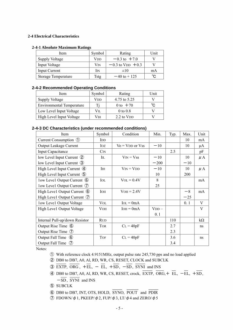
2-4 Electrical Characteristics
2-4-1 Absolute Maximum Ratings Item Symbol Rating Unit
Supply Voltage VDD -0.3 to +7.0 V Input Voltage VIN -0.3 to VDD +0.3 V Input Current IIN ±10 mA Storage Temperature Tstg -40 to + 125
2-4-2 Recommended Operating Conditions
Item Symbol Rating Unit Supply Voltage VDD 4.75 to 5.25 V Environmental Temperature Tj 0 to +70 Low Level Input Voltage VlL 0 to 0.8 V High Level Input Voltage VIH 2.2 to VDD V
2-4-3 DC Characteristics (under recommended conditions)
Item Symbol Condition Min. Typ. Max. UnitCurrent Consumption ① IDD 10 mA Output Leakage Current IOZ Vo = VDD or Vss -10 10 µA Input Capacitance CIN 2.5 pF low Level Input Current ② low Level Input Current ③
IIL VIN = Vss -10 -200
10 -10
μA
High Level Input Current ④ High Level Input Current ⑤
IIH VIN = VDD -10 10
10 200
μA
1ow Leve1 Output Current ⑥ 1ow Leve1 Output Current ⑦
IOL VOL = 0.4V 8 25
mA
High Leve1 Output Current ⑥ High Leve1 Output Current ⑦
IOH VOH = 2.4V -8 -25
mA
1ow Leve1 Output Voltage VOL IOL = 0mA 0. 1 V High Leve1 Output Voltage VOH IOH = 0mA VDD –
0. l V
Internal Pull-up/down Resistor RUD 110 kΩ Output Rise Time ⑥ Output Rise Time ⑦
TOR CL = 40pF 2.7 2.3
ns
Output Fall Time ⑥ Output Fall Time ⑦
TOF CL = 40pF 3.6 3.4
ns
Notes: ① With reference clock 4.9151MHz, output pulse rate 245,730 pps and no load applied ② DB0 to DB7, A0, Al, RD, WR, CS, RESET, CLOCK and SUBCLK ③ EXTP
, ORG
, +EL
, - EL
, +SD
, -SD
, SYNI
and INS ④ DB0 to DB7, A0, Al, RD, WR, CS, RESET, crock, EXTP
, ORG
,+ EL
, -EL
, +SD
, -SD
, SYNI
and INS ⑤ SUBCLK ⑥ DB0 to DB7, INT, OTS, HOLD, SYNO
, POUT
and PDIR
⑦ FDOWN/φ1, PKEEP/φ2, FUP/φ3, LT/φ4 and ZERO/φ5
- 6 -
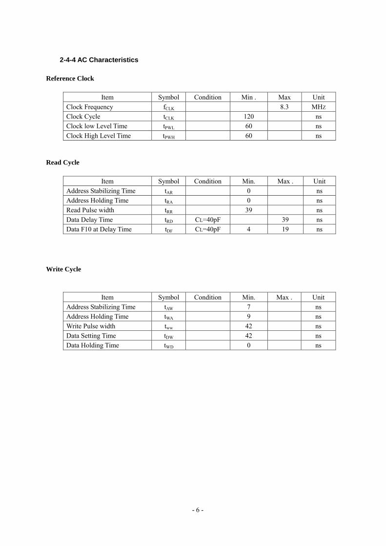
2-4-4 AC Characteristics Reference Clock
Item Symbol Condition Min . Max Unit Clock Frequency fCLK 8.3 MHZ Clock Cycle tCLK 120 ns Clock low Level Time tPWL 60 ns Clock High Level Time tPWH 60 ns
Read Cycle
Item Symbol Condition Min. Max . Unit Address Stabilizing Time tAR 0 ns Address Holding Time tRA 0 ns Read Pulse width tRR 39 ns Data Delay Time tRD CL=40pF 39 ns Data F10 at Delay Time tDF CL=40pF 4 19 ns
Write Cycle
Item Symbol Condition Min. Max . Unit Address Stabilizing Time tAW 7 ns Address Holding Time tWA 9 ns Write Pulse width tww 42 ns Data Setting Time tDW 42 ns Data Holding Time tWD 0 ns

- 7 -
Reset Cycle
Item Symbol Condition Min. Max. Unit Reset Pulsewidth tRST 3 ・ tCLK ns Reset Time tRSTM 3・ tCLK ns
Operation Tuning
Item Symbol Condition Min. Max . Unit
EL
Pulsewidth tEL 46 ns
EL
/INT Delay Time tEL1 55 ns
PRG/INT Delay Time tPl (Note l) ns
POUT
Delay Time H→L tPLD 33 ns
POUT
Delay Time L→H tHD 42 ns
CLR Delay Time tCLR (Note 2) ns ECA/B H Level Time ① tECHl 3・tCLK ECA/B H Level Time ② tECH2 1.5・tCLK ECA/B L Level Time ① tECLl 3・tCLK ECA/B L Level Time ② tECL2 l.5・tCLK
Notes: l. Synchronized with the fall of reference clock signal after completion
of operation; delay time = 48ns max. 2. Synchronized with the rise of reference clock signal; delay time = 27ns max.
① With the current position counter external input set for the A/B phase mode. ② With the current position counter external input set for the CW/CCW mode.

- 8 -
3. Input/Output Signals
3-1 Signal Functions
l) +SD
, -SD
・These signals ramps down an output pulse rate in CW and CCW directions respectively.
・When the SD
signal in the same direction as the moving direction becomes low level during high-speed operation, the pulse rate ramps down. When the signal recovers a high level, the pulse rate ramps up.
・SD
signals are invalid if they are set to "DISABLE" in the operation mode select command.
2) +EL
, -EL
・These are end-limit signals. ・When the EL
signal in the same direction as the moving direction becomes low level, pulse output stops immediately. Even when the signal recovers a high level, the stop condition is retained.
・A stop condition is retained when the EL
signal in the moving direction is already low level at the start. But take care that the INT signal is not output in such the case.
・EL
signals are invalid if pulse output is set to OFF in the extension mode.
3) ORG
・This is the origin signal. ・If the ORG
signal is set to ENABLE in the operation mode select command, the low-level ORG
signal stops pulse output immediately. If the signal recovers a high level, the stop condition is retained.
4) HOLD ・This is the HOLD signa1output to the monitor. It becomes high level when the
PCL-240AK is under the stop condition.
5) FUP/φφφφ1, ・These are signals output to the monitor. FKEEP/φφφφ2, FUP : Becomes high level during ramping-up. FDOWN/φφφφ3, FKEEP : Becomes high level under a stop or constant-speed condition LT/ φφφφ4 , FDOWN : Becomes high level during ramping-down. ZERO/φφφφ5 LT : Becomes high level when a down counter (R0) value is smaller
than a ramping-down point register (R6) value. ZERO : Becomes high level when a down counter (R0) value is 0.
・In the extension mode, these signals can be replaced with phase signals output
to stepping motors. Use φ1 through φ4 for 4-phase motors and φ1 through φ5 for 5-phase motors.
6) INT
・This is an interrupt request signal to the CPU. ・The signal is low level when a programmed operation is complete, an origin
return is complete, or pulse output stops due to an end limit, deceleration stop command or immediate stop command.
・The signal recovers the high level through software control. It can be also masked if required.
・In the extension mode, the INT
signal can be output at a start of ramping down in a programmed operation.

- 9 -
7)SYNI
/INP,,,, ・These signals are used for synchronous operation of two or more units of SYNO
/CLR PCL-240AK.Pin 11 of master PCL-240AK outputs the SYNO
signa1 and Pin 39 of slave PCL-240AK inputs SYNI
signal. ・If synchronous operation is not required, p1ace these temina1 pins in the open
condition, or pu11 up Pin 39 and open pin 11. ・1n the extension mode, these terminals can be changed to servo interface
contro1 temina1s. INP : This is the in-position signal input from the servo driver. If pulse
output is complete in a programmed operation, the INP signal is not output until it is sent from the servo driver to pin 39.
CLR : This is the deviation counter clear signa1 output to the servo driver. The pulse signal is of eight cycles of reference clock and output when an origin return is complete or pulse output stops due to an end limit.
8) EXTP
/EC-A ・This is the negative 1ogic pulse which lets down counter R0 count through an external pulse input.
・The signal is valid only if the R0 counter mode is set to EXT PULSE in the output mode select command. This negative 1ogic pulse lets the R0 counter in the EXT PULSE mode count down even when the PCL-240AK is under a stop condition.
・In the extension mode, pin 36 for the EXTP
signal can be changed to the terminal to input the encoder A-phase signa1 or CW count signal to current position counter R10
9) INS/EC-B ・This is a universal input signal and does not give any effect to the operation of
the PCL-240AK. It may be a status signal from the CPU. ・In the extension mode, pin 37 for the INS signal can be changed to the
terminal to input the encoder B-phase signa1 or CCW count signal to current position counter R10.
・This is a universa1 output signal, which can be controlled through the CPU by so setting the register select command. The OTS signal can be made high level by setting bit 3 of the register select command to l, and low level by setting it to 0.
10) OTS ・This is a universa1 output signal, which can be controlled through the CPU by
so setting the registers select command. The OTS signal can be made high level by setting bit 3 of the register select command to l, and low level by setting it to 0.
11) POUT
/PDIR
・These are pulse output signals. The output mode select command permits selection of the directory mode (direction signal and common signa1 output) or the pulse mode (CW and CCW pulses output).
・In the directory mode, the PDIR
termina1 outputs a direction signal and the POUT
termina1 outputs pulses. The direction signal is low level for the CW direction and high level for the CCW direction Pulses are output in negative logic.
- 10 -
・In the pulse mode, the POUT
termina1 outputs CW pulses and the PDIR
terminal, CCW pulses. These pulses are output in a negative 1ogic. ・In the extension mode, logics for PDIR
and POUT
can be changed and pulse output ON/OFF control is possible.
12)))) CLOCK ・This is the reference clock signal for the PCL-240AK. Usually, it is a
4.9152MHz signal. ・Take care that the accuracy of the reference clock influences the accuracy of
output pulse.
13) RESET ・This is a reset signal for the PCL-240AK. ・When the signal becomes low level during operation, pulse output stops
immediately. Take care, however, that the width of the last output pulse may not be sufficient.
・After reset, the PCL-240AK is placed in the following conditions. Start-Stop Command 00H Operation Mode Select Command 40H Register Select Command 80H Output Mode Select Command C0H Basic Operation Mode Standard mode R0 to R7. RI0 to R13 0
14) CS ・This is the chip select signal.
・The low level CS signal input to pin 6 makes RD and WR signals valid, thereby allowing the PCL-240AK to read/write from/to the CPU.
15) RD ・This is the read signal. ・low level RD signal input to pin 8 and low level CS signal to pin 6 let the
status buffer or register contents be output to input/output terminals of the data bus.
16) WR ・This is the write signal.
・When the WR signal changes from low to high level with the CS signal at low level, data on the data bus is written in the PCL-240AK via D0 through D7.
17)))) D0 to D7 ・These are data input/output to/from the 3-state data bus.
18) A0. Al ・These are address signals. ・Usually, these input signals are low-place 2 bits of the CPU address bus.
19) SUBCLK ・This is a sub-clock input signal in special applications of the extension mode.
・Usually, pin 25 for this SUBCLK signal will be connected to the GND terminal.
20) VDD, GND ・These are power input signals of 5V ±10% and GND.

- 11 -
3-2 Pins vs. Signals
Pin No. Symbol I/O Description l OTS O Universa1 output signal 2 CLOCK
I Reference clock 3, 7, 20, 26 GND I 0V (All these 4 pins should be connected to the ground.)
4 RESET
I Reset signal 5, 9 Al, A0 L Address signals 6 CS
I Chip select signal 8 RD
I Read signal 10 WR
I Write signal 11 SYNO
/CLR O Synchro. signa1 output/Servo clear signal 12 to 19 D0 to D7 I/O Data bus
21 -SD
I↑ CCW ramping-down signal
22 +SD
I↑ CW ramping-down signal
23 -EL
I↑ CCW end-limit signal
24 +EL
I↑ CW end-limit signal
25 SUBCLK l↓ Sub- clock (usually to be connected to the ground) 27 POUT
O Pulse output or CW pulse output 28 PDIR
O Direction signa1or CCW pulse output 29 HOLD O Signa1 output during stop 30 FDOWN/Ml O Signa1 output during ramping-down/Motor I-phase signal 31 FKEEP/M2 O Signa1 output during constant-speed operation / Motor
2-phase signal 32 FUP/M3 O Signa1 output during ramping-up / Motor 3-phase signal 33 LT/M4 O (R0) < (R6) / Motor 4-phase signal 34 ZERO/M5 O (R0) = 0 / Motor 5-phase signal 35 INT O* Interrupt signal 36 EXTP
/EC-A I↑ External pulse signal / Encoder A-phase signal 37 INS/EC-B I↑ Universal input signal / Encoder B-phase signal 38 ORG
I↑ Origin switching signal 39 SYNI
/INP I↑ Synchro. signal input / In-position signal 40 VDD I +5v
Remarks: I↑ : Pull-up resistor built in I↓ : Pull-down resistor built in O* : Open drain with built-in pull-up resistor (wired OR possible)

- 12 -
4.Cntents of Read & Write Data
Contents of read and write data differ with addresses. Relations among read/write data and addresses as follows.
CS
RD
WR
Al A0 Description L L H L L Data bus ← Status buffer L L H L H Data bus ← Register (bits 7 to 0) L L H H L Data bus ← (bits 15 to 8) L L H H H Data bus ← Register (bits 23 to 16) L H L L L Data bus → Command Buffer L H L L H Data bus → Register (bits 7 to 0) L H L H L Data bus → Register (bits 15 to 8) L H L H H Data bus → Register (bits 23 to 16) L L L × × Prohibit H × × × × Data bus = High impedance

- 13 -
5. Commands
5-1 Outline of Commands
Operation of the PCL-240AK requires data writing in the command buffer and registers via the 8-bit data bus.
As shown above, commands may be classified into four types according to data in high-place two bits. Contents of each command are retained until different particulars are written in the command of the same type. Each command is not a code but each bit of a command has the function. So, settings other than described below are available. Command writing order and register selecting order are flexible. However, since writing a start-stop command starts the PCL-240AK, write the command at the last.

- 14 -
5-2 Start-Stop Command
Example of Start・Stop Command
D7 D6 D5 D4 D3 D2 Dl D0 Description 0 0 0 l 0 0 0 0 FL -based constant-speed operation (with no INT signa1 output)
The PCl-240AK operates at a speed set in FL register Rl.
0 0 l l 0 0 0 0 FL -based constant-speed operation (with the INT signa1 output) 0 0 0 l 0 0 0 l FH1-based constant-speed operation (with no INT signa1 output)
The PCL-240AK operates at a speed set in FH1 register R2. 0 0 0 l 0 0 l l FH2-based constant-speed operation (with no INT signa1 output)
The PCL-240AK operates at a speed set in FH2 register R3 . 0 0 0 l 0 l 0 l FHl-based high-speed operation (with no INT signa1 output)
The PCL-240AK starts at a speed set in the FL register, then ramps up to a speed set in the FH1 register.
0 0 0 l 0 l l l FH2-based high-speed operation (with no INT signa1 output) The PCL-240AK starts at a speed set in the FL register, then ramps up to a speed set in the FH2 register.
0 0 0 l 0 l 0 0 Ramping down on the way The PCL-240AK ramps down from a speed set in the FH1 or FH2
register to a speed set in the FL register. 0 0 0 l l l l l Deceleration stop
The PCL-240AK ramps down from a speed set in the FHI or PH2 register and stops when the speed reaches what is set in the FL registers is reached. (A reset command is required after stop.)
0 0 l 0 l 0 0 0 Immediate stop (with the INT signa1 output)
0 0 0 0 l 0 0 0 Immediate stop (reset command) (with no INT signa1 output)
A speed can be changed during operation by revising the start-stop command. However, to
change a speed after ramping up or down from constant-speed operation, the operator need to effect the high-speed mode with the present speed, then write a new high-speed start-stop command.
Example: To ramp up from the FL-based constant-speed operation, then change the speed to what is set in the FH1 register.
(1) Write 14H (FL -based high-speed operation). (2) Write 15H (FH1 -based high-speed operation).

- 15 -
5-3 Operation Mode Select Command
Example of Operation Mode Select Command
D7 D6 D5 D4 D3 D2 D1 D0 Description 0 l × × × × × 0 The ORG
terminal at 1ow level does not stop pulse output.
0 l × × × × × l The 1ow-leve10RG signal to pin 38 stops pulse output.
0 l × × × × 0 × The 1ow-level SD
signal to pin 21 or 22 does not effect ramping-down.
0 l × × × × l × The low-level SD
signal to pin 21 or 22 effects ramping-down.
0 l × × × 0 × × Pulse output does not stop with R0=0.
0 l × × × l × × Pulse output stops with R0=0.
0 l × × 0 × × × Moving in CW direction.
0 1 × × 1 × × × Moving in CCW direction.
0 1 × 0 × × × × A ramping-down point is to be written in R6.
0 l × l × × × × A ramping-down point is to be set automatically.
0 l 0 × × × × × The current position counter is not operated.
0 l l × × × × × The current position counter is operated.
0 l × × × 0 0 0 Manual mode
0 1 × × × 0 × l Origin rectum mode
0 l × × × l 0 0 Programmed operation mode
Note: Mark × in the above table may be either 0 or 1 .
- 16 -
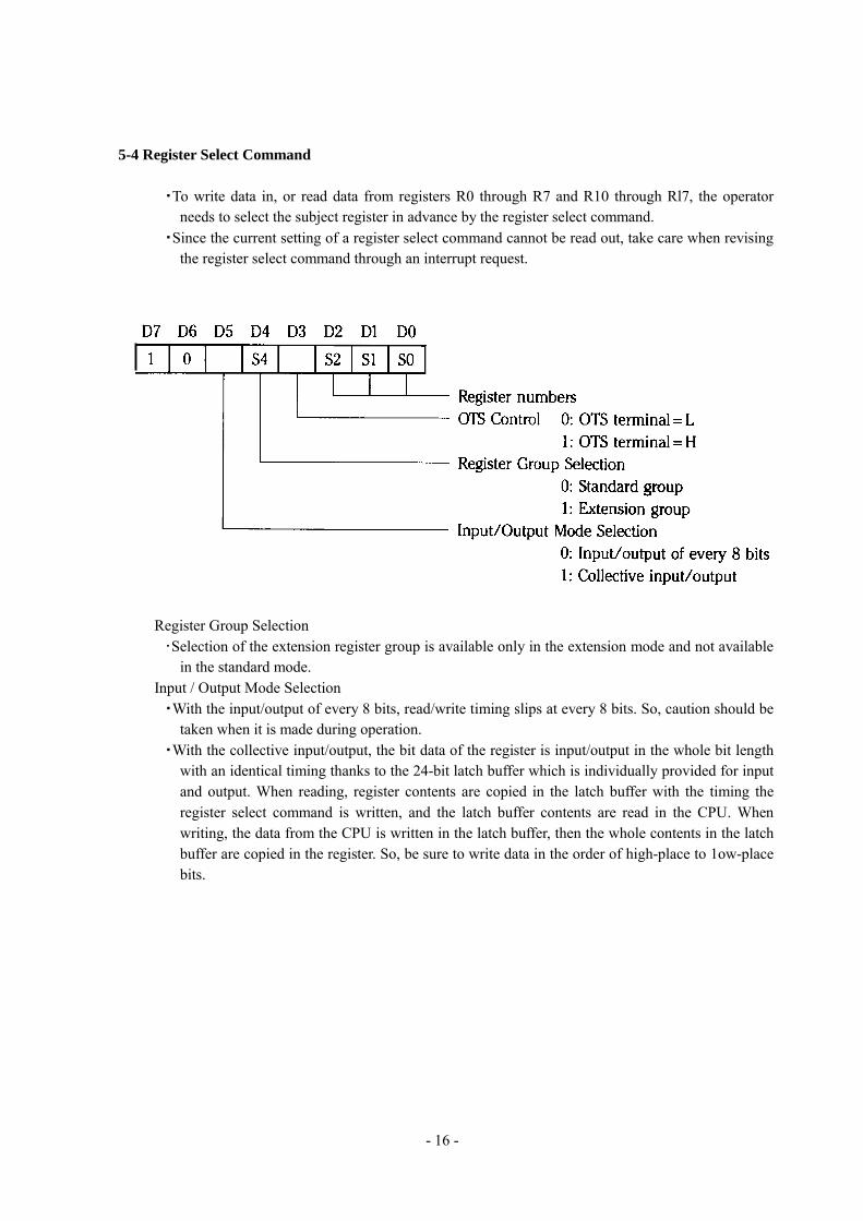
5-4 Register Select Command
・To write data in, or read data from registers R0 through R7 and R10 through Rl7, the operator needs to select the subject register in advance by the register select command.
・Since the current setting of a register select command cannot be read out, take care when revising the register select command through an interrupt request.
Register Group Selection ・Selection of the extension register group is available only in the extension mode and not available
in the standard mode. Input / Output Mode Selection ・With the input/output of every 8 bits, read/write timing slips at every 8 bits. So, caution should be
taken when it is made during operation. ・With the collective input/output, the bit data of the register is input/output in the whole bit length
with an identical timing thanks to the 24-bit latch buffer which is individually provided for input and output. When reading, register contents are copied in the latch buffer with the timing the register select command is written, and the latch buffer contents are read in the CPU. When writing, the data from the CPU is written in the latch buffer, then the whole contents in the latch buffer are copied in the register. So, be sure to write data in the order of high-place to 1ow-place bits.

- 17 -
List of Registers S4 S2 S1 S0 R No. Description Bit Length R/W 0 0 0 0 R0 Down counter 24 R/W 0 0 0 l R1 FL register 13 R/W * 0 0 l 0 R2 RHI register 13 R/W* 0 0 l 1 R3 RH2 register 13 R/W' 0 1 0 0 R4 Acceleration rate register 14 R/W* 0 l 0 l R5 Deceleration rate register 14 R/W* 0 l l 0 R6 Ramping-down point register 20 R/W* 0 l l l R7 Multiplication register 16 R/W * l 0 0 0 R10 Current position counter 24 R/W** l 0 0 l R1l Current speed monitor 13 R* * * l 0 l 0 R12 Extension mode register l 24 R/W** l 0 l l R13 Extension mode register 2 16 R/W* * l l l 0 R16 Command buffer monitor 24 R* * * l 1 l l R17 Extension status buffer 8 R***
R/W Read/write available in both standard and extension modes. R/W* Read only available in the standard mode, and read/write available in the extension mode. R/W** Unusable in the standard mode, but read/write available in the extension mode. R*** Unusable in the standard mode, but read available in the extension mode.
Example of Register Select Command D7 D6 D5 D4 D3 D2 D1 D0 Description l 0 × 0 × 0 0 0 Selects register R0. 1 0 × 0 × 0 0 L Selects register R1. l 0 × 0 × 0 l 0 Selects register R2. l 0 × 0 × 0 l L Selects register R3. l 0 × 0 × l 0 0 Selects register R4. l 0 × 0 × l 0 L Selects register R5. l 0 × 0 × l l 0 Selects register R6. l 0 × 0 × l l L Selects register R7. l 0 × l × 0 0 0 Selects register R10. l 0 × 1 × 0 0 L Selects register Rl1. l 0 × l × 0 l 0 Selects register R12. l 0 × l × 0 l 1 Selects register R13. l 0 × l × l l 0 Selects register R16. l 0 × l × l l L Selects register Rl7. l 0 × × 0 × × × Makes the OTS terminal pin low level. l 0 × × l × × × Makes the OTS terminal pin high level. l 0 0 × × × × × Selects every 8-bit input/output mode. l 0 l × × × × × Selects the collective input/output mode. Mark × in the above table may be either 0 or 1.
- 18 -
5-5 Output Mode Select Command
・The output mode select command selects and specifies the output pulse mode, down counter input signal, etc.
Synchronous Operation Control
・For synchronous operation, set this bit of the slave PCL-240AK to "1' Down Counter Input Signal ・Select the down counter (R0) input signal. If the bit is set to "0' one pulse output of the
PCL-240AK lets the R0 count down by one. If the bit is set to "1' one pulse output of the PCL-240AK does not let the R0 count down but one pulse input from the EXTP
terminal lets it count down by one.
Basic Operation Mode
・Select the basic operation mode for the PCL-240AK. The standard mode initiated by setting this bit to "0" allows controlling of the PCL-240AK like the PCL-240K. The extension mode initiated by setting this bit to "1" makes it possible to use all functions added to the PCL-240AK.
Ramping-Up/Down Control
・If an output mode command In which this bit is set to "1' is written during ramping-up or down, ramping-up or down stops and a pulse output speed is fixed. In the extension mode, the speed can be known by reading register R11.

- 19 -
Sensitivity Selection for ORG
& EL Signals Input
・ORG
, +EL
and -EL
signals can be stopped with a pulse signal. if this bit is set to "0" for high sensitivity, even a pulse of an approximately 50ns can stop these signals. If a low sensitivity is selected by setting this bit to "1' pulse signals, which are narrower than 4 cycles of reference clock (approximately 800ns with 4.9152MHz), are eliminated as noise.
Example of Output Mode Select Command Setting
D7 D6 D5 D4 D3 D2 Dl D0 Description l l x × × × × 0 Does not effect synchronous operation. l l × × × × × l Makes synchronous operation available. l l × × × × 0 × Selects the directory output mode. 1 l × × × × l × Selects the pulse output mode. l l × × × 0 × × Selects an output pulse for the down counter input. l l × × × l × × Selects an EXTP
input for the down counter input. l l × × 0 × × × Selects the standard mode. l l × × l × × × Selects the extension mode. l l × 0 × × × × Continues ramping-up/down. l l × 0 × × × × Stops ramping-up/down. l l 0 × × × × × Selects high sensitivity for ORG
and EL
signals. l l l × × × × × Selects low sensitivity for ORG
and EL
signals. Mark × in the above table may be either 0 or 1.

- 20 -
6. Registers
6-1 R0: 24-bit Down Counter
In any of the manua10rigin return and programmed modes, every one-pulse output lets the R0 count down by one. However, if the EXTP
input signal is selected for the down counter input with the output mode select command, every one pulse input to the EXTP
terminal lets the R0 count down by one.
When the R0 counts down with the counter value put at 0, it returns to a maximum value, FFFFFF in the hexadecimal progression or 16777215 in the decimal progression.
A counter value (number of remained pulses) can be read during operation in progress or cessation. However, during operation in progress, read it once and re-read immediately after then to make sure that the second reading is the same as the first one, or use the collective reading function in the extension mode.
In the programmed mode, set a desired number of output pulses in this register. After starting, the counter value will decrease as pulses are output. When the set number of pulses will be output, the counter value will be 0 and pulse output will stop.
A setting range is 000000 to FFFFFF in the hexadecimal progression, which corresponds to I to 16777215 in the decimal progression. Take care that if this counter is set at 0, writing a start-stop command does not start pulse output and while the operation status flag and HOLD output signal indicate the stop status, the INT signal is not output.
Interruption by a deceleration or immediate stop command during programmed operation does not clear the counter value. So, only inputting a second start-stop command allows outputting of remained pulses. Also, since a completion of pulse output in a set quantity makes the R0 counter value 0, the operator needs to set the R0 down counter every time even if the value is the same as the previous one.
- 21 -
6-2 R1: 13-bit FL Register
The R1 registers a low pulse rate. In high-speed operation, pulse output starts at a pulse rate set in the FL register, then is made at a pulse rate set in the FH1 or FH2 register. If a deceleration stop command is input during high-speed operation, pulse output ramps down and stops when the speed reaches what is set in the FL register.
If the FL register is set at 0, the POUT
terminal may be 1ocked to a low level when stopping, thereby making a stop status unavailable. So, be sure to set the FL register at 1 or higher value.
FH l-initiated FH2-initiated Deceleration
High-speed Start High-speed Start Stop
A setting range is 0001 to 1FFF in the hexadecimal progression, which corresponds to 1 to 8191 in the decimal progression.
Relations between a set value and output pulse rate depend on a value set in the R7 multiplication register.
6-3 R2: 13-bit FH1 Register
The FH1 registers high pulse rate 1 . A setting range is 0001 to IFFF in the hexadecimal progression, which corresponds to 1 to 8191 in the decimal progression. Relations between a set value and output pulse rate depend on a set value in the R7 multiplication register.
6-4 R3: 13-bit FH2 Register
The PH2 registers high pulse rate 2. A setting range is 0001 to 1FFF in the hexadecimal progression, which corresponds to 1 to 8191 in the decimal progression. Relations between a set value and output pulse rate depend on a set value in the R7 multiplication register.
- 22 -
6-5 R4: 14-bit Acceleration Rate Register
The R4 registers an acceleration rate (ramping-up time factor). In high-speed operation, pulse output starts at a low pulse rate set in the Rl, then accelerates to a high pulse rate set in the R2 or R3. A ramping up time, Tsu, is obtained by the following equation.
Tsu = ([R2]- [R1]) × [R5] × [TCLK] sec
Where, [R1] = Set value in R1
[R2] = Set value in R2 [R4] = Set value in R4 [TCLK] sec = Reference clock cycle
A setting range is 0002 to 3FFF in the hexadecimal progression, which corresponds to 2 to 16383 in the decimal progression.
6-6 R5: 14-bit Deceleration Rate Register
The R5 registers a deceleration rate (ramping-down time factor). In a high-speed operation, an SD
signa10r speed change command input lets pulse output ramp down. The time. Ted, required for ramping down is obtained by the following equation.
Tsd = ([R2] - [RI]) × [R5] × [TCLK] sec
A setting range is 0002 to 3FFF in the hexadecimal progression, which corresponds to 2 to 1 6383 in the decimal progression. If the automatic ramping-down point setting function is used, a set value in the R5 is discarded and that in the R4 is applied to the deceleration rate.
6-7 R6: 20-bit Ramping-down Point Register
If the automatic ramping-down point setting function is used, the operator can omit setting of this R6 register. With the automatic setting mode selected, the R6 register operates as a counter, which counts pulses required for ramping-up, and the counted value becomes data for ramping down Resetting the R6 counter is made by inputting a start-stop command of which the start control bit is set to "0" (or a reset command, etc.). Accordingly, by setting the R6 after inputting a reset command, the operator can let pulse output ramp down earlier by the set value.
f FH1
Tsu FL t

- 23 -
To operate with the automatic ramping-down point setting function set to OFF calculate the number of pulses for ramping-down and set the R6 register at that value. The number of pulses, PSD1 , for ramping-down from a pulse rate set in the FH1 register to that set in the FL register is:
( [R2 ]-[R1] )×( [R2] +[R1]-l )×[R5]
PSD1= 16384× [R7]
The number of pulses, PSD2, for ramping-down from a pulse rate set in the PH2 register to that set in the FL register is:
([R3]-[R1])×([R3] +[R1]-l)×[R5]
PSD2 = l 6384 × [R7]
6-8 R7: 16-bit Multiplication Register
While a value, which can be registered in pulse rate registers R1, R2 and R3 is limited to a range of 1 to 8191 , this R7 multiplication register allows the operator to select a multiplication factor, that is, decide the relations between a set value in each register and an output pulse rate. Output pulse rate PPOUT (pps) is obtained by the following equation.
(FCLOCK × RF)
PPOUT = 8192 × [R7]
Where, FCLOCK = Reference clock frequency (Hz) RF = Set value in frequency register [R7] = Set value in multiplication register
Supposing the reference clock frequency is 4.9152MHz;
0.5x mode when the R7 is set at 1200 (= 4B0HEX) lx mode when the R7 is set at 600 (= 258HEx) 2x mode when the R7 is set at 300 (= 12CHEX) 5x mode when the R7 is set at 120 (= 078HEx) 10x mode when the R7 is set at 60 (= 03CHEX) 30x mode when the R7 is set at 20 (= 014HEX)
A setting range is 0002 to FFFF in the hexadecimal progression, which corresponds to 2 to 65535 in the decimal progression.
- 24 -
6-9 R10: 24-bit Current Position Counter
This counter is usable only for the extension mode. Extension mode register I allows the operator to select an output pulse or external input pulse for the input of this counter. With any input mode selected, a counting unit can be selected, thereby allowing the R10 to count one, for example, by every 5 pulses output. With the external pulse mode selected, the operator can further select A or B phase input and CW or CCW pulse input.
When letting it count down from 000000HEX, the counter value becomes FFFFFFHEX, and when letting it count up from FFFFFFHEX, the counter value becomes 000000HEx. Since no reset function is provided for this counter, write 000000HEX to reset the counter to 0.
6-10 R11: 13-bit Current Frequency Monitor
This monitor is usable only for the extension mode. It allows the operator to read the current frequency as the number of steps in a range of I to 8191.
6-11 R12: 24-bit Extension Mode Register l
This register is usable only for the extension mode. It registers particulars of the current position counter, phase distribution function for stepping motors, etc.

- 25 -
Example of Extension Mode Command 1 (Bits 7 to 1) D7 D6 D5 D4 D3 D2 D1 D0 Description × × × × 0 0 0 0 Counting unit for current position counter = 1 pulse/count × × × × 0 0 0 l Counting unit for current position counter = 2 pulses/count × × × × 1 0 l 0 Counting unit for current position counter = 3 Pulses/count × × × × 0 0 l l Counting unit for current position counter = 4 Pulses/count × × × × 0 l 0 0 Counting unit for current position counter = 5 Pulses/count × × × × 0 l 0 l Counting unit for current position counter = 6 Pulses/count × × × × 0 l l 0 Counting unit for current position counter = 7 Pulses/count × × × × 0 l l l Counting unit for current position counter = 8 Pulses/count × × × × l 0 0 0 Counting unit for current position counter = 9 Pulses/count × × × × l 0 0 l Counting unit for current position counter = 10 pulses/count × × × × l 0 l 0 Counting unit for current position counter = 11 pulses/count × × × × l 0 l 1 Counting unit for current position counter = 12 pulses/count × × × × l l 0 0 Counting unit for current position counter = 13 pulses/count × × × × l l 0 l Counting unit for current position counter = 14 Pulses/count × × × × l l l 0 Counting unit for current position counter = 15 Pulses/count × × × × l l l l Counting unit for current position counter = 16 Pulses/count 0 × × × × × × × Input signal to current position counter = Output pulse l 0 × × × × × × Input signal to current position counter = CW and CCW pulses
l l 0 × × × × × Input signal to current position counter = A/B phase with multiplication
l 1 l 0 × × × × Input signal to current position counter = A/B phase, 2x multiplication
l l l l × × × × Input signal to current position counter = A/B phase 4x multiplicat10n
Mark × in the above table may be either 0 or 1.
- 26 -
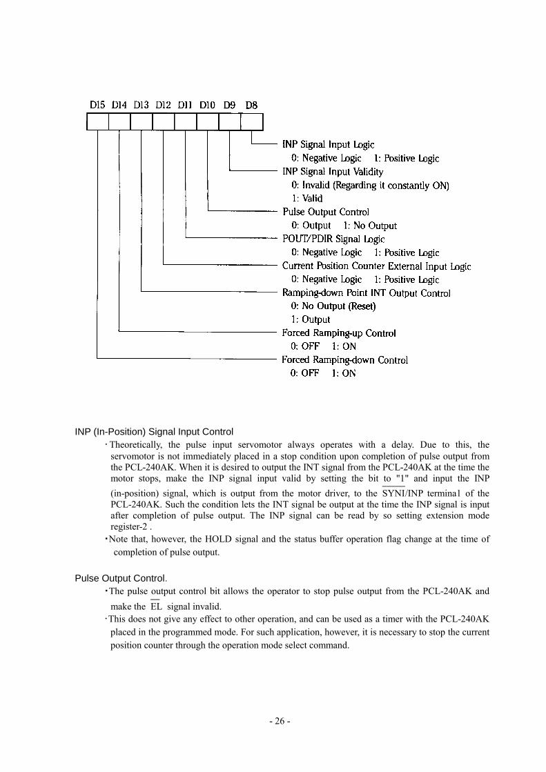
INP (In-Position) Signal Input Control ・Theoretically, the pulse input servomotor always operates with a delay. Due to this, the
servomotor is not immediately placed in a stop condition upon completion of pulse output from the PCL-240AK. When it is desired to output the INT signal from the PCL-240AK at the time the motor stops, make the INP signal input valid by setting the bit to "1" and input the INP (in-position) signal, which is output from the motor driver, to the SYNI
/INP termina1 of the PCL-240AK. Such the condition lets the INT signal be output at the time the INP signal is input after completion of pulse output. The INP signal can be read by so setting extension mode register-2 .
・Note that, however, the HOLD signal and the status buffer operation flag change at the time of completion of pulse output.
Pulse Output Control.
・The pulse output control bit allows the operator to stop pulse output from the PCL-240AK and make the EL
signal invalid. ・This does not give any effect to other operation, and can be used as a timer with the PCL-240AK
placed in the programmed mode. For such application, however, it is necessary to stop the current position counter through the operation mode select command.

- 27 -
Ramping-Down Point INT Output Control ・In the programmed high-speed operation, this allows the INT signal to be output even at the start
of ramping-down. ・In such the case, an interrupt signal at a stop and that at the start of ramping-Down are ORed to be
output from the INT terminal. Judge which interrupt signal is output from the INT terminal, through bits l and 0 of the extension status buffer.
Forced Ramping-up Control
・This allows forced ramping-up from the current speed to a maximum speed (step 8191) with the set acceleration rate. By setting this control bit to OPF during ramping-up, the operator can keep the speed at that time and read it through the R11 register.
・To effect the forced ramping-up, write an output mode select command which stops ramping-up / down. Also, do not set forced ramping-up and forced ramping-down bits to ON at the same time. Forced Ramping-down Control
・This allows forced ramping-down from the current speed to a minimum speed (step 0 ) with the set deceleration rate. By setting this control bit to OFF during ramping-down, the operator can keep the speed at that time and read it through the R11 register.
・To effect the forced ramping-down, write an output mode command which stops ramping-up / down. Also, do not set forced ramping-up and forced ramping-down bits to ON at the same time.
Example of Extension Mode Command 1 (Bits 1 5 to 8)
Dl5 D14 D13 Dl2 D11 D10 D9 D8 Description × × × × × × × 0 Makes the INP signal input 1ogic negative. × × × × × × × l Makes the INP signal input 1ogic positive. × × × × × × 0 × Makes the INP signal discarded (regarding it always ON) × × × × × × l × Makes the INP signal valid. × × × × × 0 × × Lets the POUT
(PDIR
) termina1 output pulses. × × × × × l × × Stops the POUT
(PDIR
) terminal from outputting pulses. × × × × 0 × × × Makes the POUT
(PDIR
) output 10gic negative. × × × × l × × × Makes the POUT
(PDIR
) output 10gic positive.
× × × 0 × × × × Makes the current position counter external input 10gic negative.
× × × l × × × × Makes the current position counter external input 10gic positive.
× × 0 × × × × × Makes the INT signal not output at the start of ramping-down.
× × l × × × × ×Makes the INT signa1 output even at the start of ramping-down.
× o × × × × × × Does not effect forced ramping-up. 0 l × × × × × × Effects forced ramping-up. 0 × × × × × × × Does not effect forced ramping-down. l 0 × × × × × × Effects forced ramping-down.
Mark × in the above table may be either 0 or l.

- 28 -
Phase Output Bit Pattern ・Bits D16 to D20, which correspond to terminals φ1 through φ5, are for setting initial values of
the output pattern at these terminals. Terminals of which the bits are set to I , output high-level signals.
・For 4-phase motors, bit D20 may be set to either 0 or 1 . ・The pattern information which is read, is not the pattern of the initial values but the current pattern
which changes from the initia10ne due to operation.
Step Control ・When the full step is selected, the number of the terminals which output high-level signals, is
made constant as in the case of 2-2-phase excitation. ・ When the half step is selected, the number of the terminals which output high-level signals,
changes as in the case of I -2-phase excitation.
Number of Phases ・The number of phases can be selected through this bit. ・The pattern is output at terminalsφ1 throughφ4 with 4 phases selected, and at terminals φ1
throughφ5 with 5 phases selected.
Output Terminal Signals ・Signals output at terminals 30 through 34 are selected through this bit. ・Since the phase distribution circuit operates constantly, the phase output bit pattern which changes
a long with operation, can be read if the phase output is not made valid.

- 29 -
Examples of Phase Output Change

- 30 -
6-12 R13: 16-bit Extension Mode Register 2
The R13 register is provided for setting CLR signal particulars and for special control modes. The register is usable only for the extension mode.
CLR Signal
・ Theoretically, the pulse input servomotor operates with a delay from an input pulse. Accordingly, if the origin switch is turned on in the origin return mode to stop the PCL-240AK from outputting pulses, the servomotor does not stop at the same time but rotates by delay, thereby making the accuracy of origin inferior. To prevent this, the servomotor is provided with a deviation clear signal input for immediate stop. The CLR signal is a pulse signal to produce the deviation clear signal.
・ The CLR signal is output when the ORG
signal is on in the origin return mode or when the EL
signal is on, or through manual control. With the manual control, an output time of the CLR signal can be changed through the CPU program, but an output time of the ORG
or EL
signal initiated CLR signal is constant-8 cycles of the reference clock frequency of the PCL-240AK (approximately I .6us with 4.9152MHz). So, the operator may need to expand the pulse width through an external circuit depending on the specifications of the servomotor.
Example of Extension Mode Command 2 (Bite 7 to O) D7 D6 D5 D4 D3 D2 Dl D0 Description 0 0 0 0 × × × × Makes the CLR signal unused. 0 0 0 l × × × 0 Makes the manual CLR signa1OFF. 0 0 0 l × × × l Makes the manual CLR signa1ON. 0 0 0 l × × l 0 Outputs the CLR signal with the EL
signal ON. 0 0 0 l × l × 0 Outputs the CLR signal with origin return complete. 0 0 0 l 0 × × × Makes the CLR signal 1ogic negative. 0 0 0 1 l × × × Makes the CLR signal 1ogic positive.
Mark × in the above table may be either 0 or l.

- 31 -
Acceleration/Deceleration Time Control Mode ・ The PCL-240AK provides linear ramping-up/down, because the frequency-constant reference
clock is used as a ramping-up / down control clock. Curvilinear ramping-up / down is made available by inputting an external clock signa1 of which the frequency changes while disusing the reference clock as a ramping-up / down control clock. The external clock signal input is the SUBCLK terminal.
・ An external clock signal, which is input to the SUBCLK terminal after the pulse output rate reaches what is registered in FL 0r FH register, is discarded.
Ramping-up Control Mode ・ With the PCL-240AK, ramping-up is controlled by a parameter set in the R4 acceleration rate
register. Also, the operator can externally control ramping-up by inputting one clock signal to the SUBCLK terminal. Every one-clock signal accelerates pulse output by one step.
・ A clock signal, which is input after a maximum speed (step 8191), is discarded.
Example of Extension Mode Command 2 (Bits 1 5 to 8) D15 Dl 4 D1 3 Dl 2 D11 D10 D9 D8 Description 0 × × 0 0 0 0 0 Effects the internal contro1 of all ramping-up / down. 0 × × 0 0 0 0 l Effects the external contro1 of acceleration /declaration. 0 × × 0 0 0 l 0 Effects the external contro1 of ramping-up. 0 × × 0 0 l 0 0 Effect the external contro1 of ramping-down. 0 × 0 0 0 × × × Makes the SUBCLK input 1ogic negative. 0 × l 0 0 × × × Makes the SUBCLK input 1ogic positive. 0 0 × 0 0 × × × Makes status bit 5 the INS signal monitor. 0 l × 0 0 × × × Makes status bit 5 the SYNI
/ INP signal monitor. M ark × in the above table may be either 0 or 1 .

- 32 -
6-13 R16: 24-bit Command Buffer Monitor
The R16 command buffer monitor is usable only for the extension mode. The monitor allows the operator to read particulars written in the command buffer, excluding particulars written in the register select command.
6-14 R17: 8-bit Extension Status Buffer
The R17 buffer is usable only for the extension mode. It allows the operator to monitor signal status as follows.

- 33 -
7. Status Read
・ To control the status of the PCL-240AK, the operator can read the status of external and internal signals from the CPU.
・ In the extension mode, the operator can read the contents in extension status register R17 in addition to the following.
*The INS or INP terminal can be selected by so setting bit 14 of extension mode register 2. In the standard mode, it is the INS terminal.

- 34 -
8. Timing Charts
CLOCK
Read Cycle 1 (CS = VLL)
Read Cycle 2(RD = VLL)
Write Cycle 1 (CS = VLL)
Write Cycle 2 (WR = VLL)

- 35 -
Reset Cycle Timing
INT Output Timing
In the programmed mode, the INT signal is synchronized with a change of clock signal from L to H level after the final pulse output is complete.
POUT
Timing
EC-A/B Timing (in A/B Phase Input Mode)
- 36 -
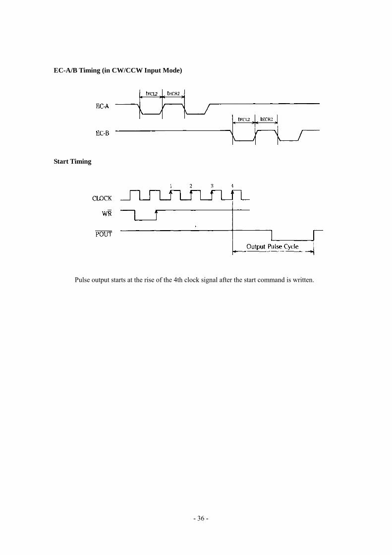
EC-A/B Timing (in CW/CCW Input Mode)
Start Timing
Pulse output starts at the rise of the 4th clock signal after the start command is written.

MNAL No. PCL-240AK-xxx-4906-2(4012)O—2000:6:13IZM