pci1520/pci1520i ghk/zhk/pdv pc card controllers datasheet
TRANSCRIPT

March 2004 PCIBus Solutions
Data Manual
SCPS065D

iii
ContentsSection Title Page
1 Introduction 1−1. . . . . . . . . . . . . . . . . . . . . . . . . . . . . . . . . . . . . . . . . . . . . . . . . . . . . . 1.1 Description 1−1. . . . . . . . . . . . . . . . . . . . . . . . . . . . . . . . . . . . . . . . . . . . . . . . . 1.2 Features 1−1. . . . . . . . . . . . . . . . . . . . . . . . . . . . . . . . . . . . . . . . . . . . . . . . . . . 1.3 Related Documents 1−2. . . . . . . . . . . . . . . . . . . . . . . . . . . . . . . . . . . . . . . . . . 1.4 Trademarks 1−2. . . . . . . . . . . . . . . . . . . . . . . . . . . . . . . . . . . . . . . . . . . . . . . . . 1.5 Ordering Information 1−2. . . . . . . . . . . . . . . . . . . . . . . . . . . . . . . . . . . . . . . . . 1.6 PCI1520 Data Manual Document History 1−3. . . . . . . . . . . . . . . . . . . . . . .
2 Terminal Descriptions 2−1. . . . . . . . . . . . . . . . . . . . . . . . . . . . . . . . . . . . . . . . . . . . . 3 Feature/Protocol Descriptions 3−1. . . . . . . . . . . . . . . . . . . . . . . . . . . . . . . . . . . . .
3.1 Power Supply Sequencing 3−1. . . . . . . . . . . . . . . . . . . . . . . . . . . . . . . . . . . . 3.2 I/O Characteristics 3−2. . . . . . . . . . . . . . . . . . . . . . . . . . . . . . . . . . . . . . . . . . . 3.3 Clamping Voltages 3−2. . . . . . . . . . . . . . . . . . . . . . . . . . . . . . . . . . . . . . . . . . . 3.4 Peripheral Component Interconnect (PCI) Interface 3−2. . . . . . . . . . . . . .
3.4.1 PCI GRST Signal 3−2. . . . . . . . . . . . . . . . . . . . . . . . . . . . . . . . . . . 3.4.2 PCI Bus Lock (LOCK) 3−3. . . . . . . . . . . . . . . . . . . . . . . . . . . . . . . 3.4.3 Loading Subsystem Identification 3−3. . . . . . . . . . . . . . . . . . . . .
3.5 PC Card Applications 3−4. . . . . . . . . . . . . . . . . . . . . . . . . . . . . . . . . . . . . . . . 3.5.1 PC Card Insertion/Removal and Recognition 3−4. . . . . . . . . . . 3.5.2 P2C Power-Switch Interface (TPS222X) 3−4. . . . . . . . . . . . . . . 3.5.3 Zoomed Video Support 3−5. . . . . . . . . . . . . . . . . . . . . . . . . . . . . . 3.5.4 Standardized Zoomed-Video Register Model 3−7. . . . . . . . . . . 3.5.5 Internal Ring Oscillator 3−8. . . . . . . . . . . . . . . . . . . . . . . . . . . . . . 3.5.6 Integrated Pullup Resistors 3−8. . . . . . . . . . . . . . . . . . . . . . . . . . 3.5.7 SPKROUT and CAUDPWM Usage 3−9. . . . . . . . . . . . . . . . . . . 3.5.8 LED Socket Activity Indicators 3−10. . . . . . . . . . . . . . . . . . . . . . . . 3.5.9 CardBus Socket Registers 3−10. . . . . . . . . . . . . . . . . . . . . . . . . . .
3.6 Serial-Bus Interface 3−11. . . . . . . . . . . . . . . . . . . . . . . . . . . . . . . . . . . . . . . . . . 3.6.1 Serial-Bus Interface Implementation 3−11. . . . . . . . . . . . . . . . . . . 3.6.2 Serial-Bus Interface Protocol 3−11. . . . . . . . . . . . . . . . . . . . . . . . . 3.6.3 Serial-Bus EEPROM Application 3−13. . . . . . . . . . . . . . . . . . . . . . 3.6.4 Accessing Serial-Bus Devices Through Software 3−14. . . . . . .
3.7 Programmable Interrupt Subsystem 3−15. . . . . . . . . . . . . . . . . . . . . . . . . . . . 3.7.1 PC Card Functional and Card Status Change
Interrupts 3−15. . . . . . . . . . . . . . . . . . . . . . . . . . . . . . . . . . . . . . . . . 3.7.2 Interrupt Masks and Flags 3−17. . . . . . . . . . . . . . . . . . . . . . . . . . . 3.7.3 Using Parallel IRQ Interrupts 3−17. . . . . . . . . . . . . . . . . . . . . . . . . 3.7.4 Using Parallel PCI Interrupts 3−18. . . . . . . . . . . . . . . . . . . . . . . . .

iv
3.7.5 Using Serialized IRQSER Interrupts 3−18. . . . . . . . . . . . . . . . . . . 3.7.6 SMI Support in the PCI1520 3−18. . . . . . . . . . . . . . . . . . . . . . . . . .
3.8 Power Management Overview 3−19. . . . . . . . . . . . . . . . . . . . . . . . . . . . . . . . 3.8.1 Integrated Low-Dropout Voltage Regulator (LDO-VR) 3−19. . . . 3.8.2 Clock Run Protocol 3−19. . . . . . . . . . . . . . . . . . . . . . . . . . . . . . . . . 3.8.3 CardBus PC Card Power Management 3−20. . . . . . . . . . . . . . . . 3.8.4 16-Bit PC Card Power Management 3−20. . . . . . . . . . . . . . . . . . . 3.8.5 Suspend Mode 3−20. . . . . . . . . . . . . . . . . . . . . . . . . . . . . . . . . . . . . 3.8.6 Requirements for Suspend Mode 3−21. . . . . . . . . . . . . . . . . . . . . 3.8.7 Ring Indicate 3−21. . . . . . . . . . . . . . . . . . . . . . . . . . . . . . . . . . . . . . . 3.8.8 PCI Power Management 3−22. . . . . . . . . . . . . . . . . . . . . . . . . . . . . 3.8.9 CardBus Bridge Power Management 3−23. . . . . . . . . . . . . . . . . . 3.8.10 ACPI Support 3−24. . . . . . . . . . . . . . . . . . . . . . . . . . . . . . . . . . . . . . 3.8.11 Master List of PME Context Bits and Global
Reset-Only Bits 3−25. . . . . . . . . . . . . . . . . . . . . . . . . . . . . . . . . . . . . 4 PC Card Controller Programming Model 4−1. . . . . . . . . . . . . . . . . . . . . . . . . . . .
4.1 PCI Configuration Registers (Functions 0 and 1) 4−1. . . . . . . . . . . . . . . . . 4.2 Vendor ID Register 4−2. . . . . . . . . . . . . . . . . . . . . . . . . . . . . . . . . . . . . . . . . . 4.3 Device ID Register 4−2. . . . . . . . . . . . . . . . . . . . . . . . . . . . . . . . . . . . . . . . . . . 4.4 Command Register 4−3. . . . . . . . . . . . . . . . . . . . . . . . . . . . . . . . . . . . . . . . . . 4.5 Status Register 4−4. . . . . . . . . . . . . . . . . . . . . . . . . . . . . . . . . . . . . . . . . . . . . . 4.6 Revision ID Register 4−5. . . . . . . . . . . . . . . . . . . . . . . . . . . . . . . . . . . . . . . . . 4.7 PCI Class Code Register 4−5. . . . . . . . . . . . . . . . . . . . . . . . . . . . . . . . . . . . . 4.8 Cache Line Size Register 4−5. . . . . . . . . . . . . . . . . . . . . . . . . . . . . . . . . . . . . 4.9 Latency Timer Register 4−6. . . . . . . . . . . . . . . . . . . . . . . . . . . . . . . . . . . . . . . 4.10 Header Type Register 4−6. . . . . . . . . . . . . . . . . . . . . . . . . . . . . . . . . . . . . . . . 4.11 BIST Register 4−6. . . . . . . . . . . . . . . . . . . . . . . . . . . . . . . . . . . . . . . . . . . . . . . 4.12 CardBus Socket/ExCA Base-Address Register 4−7. . . . . . . . . . . . . . . . . . 4.13 Capability Pointer Register 4−7. . . . . . . . . . . . . . . . . . . . . . . . . . . . . . . . . . . . 4.14 Secondary Status Register 4−8. . . . . . . . . . . . . . . . . . . . . . . . . . . . . . . . . . . 4.15 PCI Bus Number Register 4−9. . . . . . . . . . . . . . . . . . . . . . . . . . . . . . . . . . . . 4.16 CardBus Bus Number Register 4−9. . . . . . . . . . . . . . . . . . . . . . . . . . . . . . . . 4.17 Subordinate Bus Number Register 4−9. . . . . . . . . . . . . . . . . . . . . . . . . . . . . 4.18 CardBus Latency Timer Register 4−10. . . . . . . . . . . . . . . . . . . . . . . . . . . . . . 4.19 Memory Base Registers 0, 1 4−10. . . . . . . . . . . . . . . . . . . . . . . . . . . . . . . . . . 4.20 Memory Limit Registers 0, 1 4−11. . . . . . . . . . . . . . . . . . . . . . . . . . . . . . . . . . 4.21 I/O Base Registers 0, 1 4−11. . . . . . . . . . . . . . . . . . . . . . . . . . . . . . . . . . . . . . . 4.22 I/O Limit Registers 0, 1 4−12. . . . . . . . . . . . . . . . . . . . . . . . . . . . . . . . . . . . . . . 4.23 Interrupt Line Register 4−12. . . . . . . . . . . . . . . . . . . . . . . . . . . . . . . . . . . . . . . 4.24 Interrupt Pin Register 4−13. . . . . . . . . . . . . . . . . . . . . . . . . . . . . . . . . . . . . . . . 4.25 Bridge Control Register 4−14. . . . . . . . . . . . . . . . . . . . . . . . . . . . . . . . . . . . . . 4.26 Subsystem Vendor ID Register 4−15. . . . . . . . . . . . . . . . . . . . . . . . . . . . . . . . 4.27 Subsystem ID Register 4−15. . . . . . . . . . . . . . . . . . . . . . . . . . . . . . . . . . . . . . . 4.28 PC Card 16-Bit I/F Legacy-Mode Base Address Register 4−15. . . . . . . . .

v
4.29 System Control Register 4−16. . . . . . . . . . . . . . . . . . . . . . . . . . . . . . . . . . . . . . 4.30 Multifunction Routing Register 4−19. . . . . . . . . . . . . . . . . . . . . . . . . . . . . . . . 4.31 Retry Status Register 4−21. . . . . . . . . . . . . . . . . . . . . . . . . . . . . . . . . . . . . . . . 4.32 Card Control Register 4−22. . . . . . . . . . . . . . . . . . . . . . . . . . . . . . . . . . . . . . . . 4.33 Device Control Register 4−23. . . . . . . . . . . . . . . . . . . . . . . . . . . . . . . . . . . . . . 4.34 Diagnostic Register 4−24. . . . . . . . . . . . . . . . . . . . . . . . . . . . . . . . . . . . . . . . . . 4.35 Capability ID Register 4−25. . . . . . . . . . . . . . . . . . . . . . . . . . . . . . . . . . . . . . . . 4.36 Next-Item Pointer Register 4−25. . . . . . . . . . . . . . . . . . . . . . . . . . . . . . . . . . . . 4.37 Power-Management Capabilities Register 4−26. . . . . . . . . . . . . . . . . . . . . . 4.38 Power-Management Control/Status Register 4−27. . . . . . . . . . . . . . . . . . . . 4.39 Power-Management Control/Status Register Bridge
Support Extensions 4−28. . . . . . . . . . . . . . . . . . . . . . . . . . . . . . . . . . . . . . . . . . 4.40 Power-Management Data Register 4−28. . . . . . . . . . . . . . . . . . . . . . . . . . . . 4.41 General-Purpose Event Status Register 4−29. . . . . . . . . . . . . . . . . . . . . . . . 4.42 General-Purpose Event Enable Register 4−30. . . . . . . . . . . . . . . . . . . . . . . 4.43 General-Purpose Input Register 4−31. . . . . . . . . . . . . . . . . . . . . . . . . . . . . . . 4.44 General-Purpose Output Register 4−32. . . . . . . . . . . . . . . . . . . . . . . . . . . . . 4.45 Serial-Bus Data Register 4−32. . . . . . . . . . . . . . . . . . . . . . . . . . . . . . . . . . . . . 4.46 Serial-Bus Index Register 4−33. . . . . . . . . . . . . . . . . . . . . . . . . . . . . . . . . . . . . 4.47 Serial-Bus Slave Address Register 4−33. . . . . . . . . . . . . . . . . . . . . . . . . . . . . 4.48 Serial-Bus Control and Status Register 4−34. . . . . . . . . . . . . . . . . . . . . . . . .
5 ExCA Compatibility Registers (Functions 0 and 1) 5−1. . . . . . . . . . . . . . . . . . 5.1 ExCA Identification and Revision Register 5−5. . . . . . . . . . . . . . . . . . . . . . 5.2 ExCA Interface Status Register 5−6. . . . . . . . . . . . . . . . . . . . . . . . . . . . . . . . 5.3 ExCA Power Control Register 5−7. . . . . . . . . . . . . . . . . . . . . . . . . . . . . . . . . 5.4 ExCA Interrupt and General Control Register 5−8. . . . . . . . . . . . . . . . . . . 5.5 ExCA Card Status-Change Register 5−9. . . . . . . . . . . . . . . . . . . . . . . . . . . 5.6 ExCA Card Status-Change Interrupt Configuration Register 5−10. . . . . . . 5.7 ExCA Address Window Enable Register 5−11. . . . . . . . . . . . . . . . . . . . . . . . 5.8 ExCA I/O Window Control Register 5−12. . . . . . . . . . . . . . . . . . . . . . . . . . . . 5.9 ExCA I/O Windows 0 and 1 Start-Address Low-Byte Registers 5−13. . . . 5.10 ExCA I/O Windows 0 and 1 Start-Address High-Byte Registers 5−13. . . . 5.11 ExCA I/O Windows 0 and 1 End-Address Low-Byte Registers 5−14. . . . . 5.12 ExCA I/O Windows 0 and 1 End-Address High-Byte Registers 5−14. . . . 5.13 ExCA Memory Windows 0−4 Start-Address Low-Byte Registers 5−15. . . 5.14 ExCA Memory Windows 0−4 Start-Address High-Byte Registers 5−16. . . 5.15 ExCA Memory Windows 0−4 End-Address Low-Byte Registers 5−17. . . . 5.16 ExCA Memory Windows 0−4 End-Address High-Byte Registers 5−18. . . 5.17 ExCA Memory Windows 0−4 Offset-Address Low-Byte Registers 5−19. . 5.18 ExCA Memory Windows 0−4 Offset-Address High-Byte Registers 5−20. 5.19 ExCA Card Detect and General Control Register 5−21. . . . . . . . . . . . . . . . 5.20 ExCA Global Control Register 5−22. . . . . . . . . . . . . . . . . . . . . . . . . . . . . . . . . 5.21 ExCA I/O Windows 0 and 1 Offset-Address Low-Byte Registers 5−23. . . 5.22 ExCA I/O Windows 0 and 1 Offset-Address High-Byte Registers 5−23. . .

vi
5.23 ExCA Memory Windows 0−4 Page Registers 5−24. . . . . . . . . . . . . . . . . . . 6 CardBus Socket Registers (Functions 0 and 1) 6−1. . . . . . . . . . . . . . . . . . . . . .
6.1 Socket Event Register 6−2. . . . . . . . . . . . . . . . . . . . . . . . . . . . . . . . . . . . . . . 6.2 Socket Mask Register 6−3. . . . . . . . . . . . . . . . . . . . . . . . . . . . . . . . . . . . . . . . 6.3 Socket Present-State Register 6−4. . . . . . . . . . . . . . . . . . . . . . . . . . . . . . . . 6.4 Socket Force Event Register 6−6. . . . . . . . . . . . . . . . . . . . . . . . . . . . . . . . . . 6.5 Socket Control Register 6−8. . . . . . . . . . . . . . . . . . . . . . . . . . . . . . . . . . . . . . 6.6 Socket Power-Management Register 6−9. . . . . . . . . . . . . . . . . . . . . . . . . .
7 Electrical Characteristics 7−1. . . . . . . . . . . . . . . . . . . . . . . . . . . . . . . . . . . . . . . . . . 7.1 Absolute Maximum Ratings Over Operating Temperature Ranges 7−1. 7.2 Recommended Operating Conditions 7−2. . . . . . . . . . . . . . . . . . . . . . . . . . 7.3 Electrical Characteristics Over Recommended
Operating Conditions 7−3. . . . . . . . . . . . . . . . . . . . . . . . . . . . . . . . . . . . . . . . 7.4 PCI Clock/Reset Timing Requirements Over Recommended
Ranges of Supply Voltage and Operating Free-Air Temperature 7−3. . . 7.5 PCI Timing Requirements Over Recommended Ranges of
Supply Voltage and Operating Free-Air Temperature 7−4. . . . . . . . . . . . . 8 Mechanical Information 8−1. . . . . . . . . . . . . . . . . . . . . . . . . . . . . . . . . . . . . . . . . . .

vii
List of IllustrationsFigure Title Page
2−1 PCI1520 GHK-Package Terminal Diagram 2−1. . . . . . . . . . . . . . . . . . . . . . . . . . . 2−2 PCI1520 PDV-Package Terminal Diagram 2−2. . . . . . . . . . . . . . . . . . . . . . . . . . . . 3−1 PCI1520 Simplified Block Diagram 3−1. . . . . . . . . . . . . . . . . . . . . . . . . . . . . . . . . . 3−2 3-State Bidirectional Buffer 3−2. . . . . . . . . . . . . . . . . . . . . . . . . . . . . . . . . . . . . . . . . 3−3 TPS222X Typical Application 3−5. . . . . . . . . . . . . . . . . . . . . . . . . . . . . . . . . . . . . . . 3−4 Zoomed Video Implementation Using the PCI1520 3−6. . . . . . . . . . . . . . . . . . . . 3−5 Zoomed Video Switching Application 3−6. . . . . . . . . . . . . . . . . . . . . . . . . . . . . . . . 3−6 Sample Application of SPKROUT and CAUDPWM 3−10. . . . . . . . . . . . . . . . . . . . 3−7 Two Sample LED Circuits 3−10. . . . . . . . . . . . . . . . . . . . . . . . . . . . . . . . . . . . . . . . . . 3−8 Serial EEPROM Application 3−11. . . . . . . . . . . . . . . . . . . . . . . . . . . . . . . . . . . . . . . . 3−9 Serial-Bus Start/Stop Conditions and Bit Transfers 3−12. . . . . . . . . . . . . . . . . . . . 3−10 Serial-Bus Protocol Acknowledge 3−12. . . . . . . . . . . . . . . . . . . . . . . . . . . . . . . . . . 3−11 Serial-Bus Protocol − Byte Write 3−13. . . . . . . . . . . . . . . . . . . . . . . . . . . . . . . . . . . 3−12 Serial-Bus Protocol − Byte Read 3−13. . . . . . . . . . . . . . . . . . . . . . . . . . . . . . . . . . . 3−13 EEPROM Interface Doubleword Data Collection 3−13. . . . . . . . . . . . . . . . . . . . . 3−14 IRQ Implementation 3−18. . . . . . . . . . . . . . . . . . . . . . . . . . . . . . . . . . . . . . . . . . . . . . 3−15 Signal Diagram of Suspend Function 3−21. . . . . . . . . . . . . . . . . . . . . . . . . . . . . . . 3−16 RI_OUT Functional Diagram 3−22. . . . . . . . . . . . . . . . . . . . . . . . . . . . . . . . . . . . . . 3−17 Block Diagram of a Status/Enable Cell 3−24. . . . . . . . . . . . . . . . . . . . . . . . . . . . . . 5−1 ExCA Register Access Through I/O 5−1. . . . . . . . . . . . . . . . . . . . . . . . . . . . . . . . . 5−2 ExCA Register Access Through Memory 5−2. . . . . . . . . . . . . . . . . . . . . . . . . . . . . 6−1 Accessing CardBus Socket Registers Through PCI Memory 6−1. . . . . . . . . . . .
viii
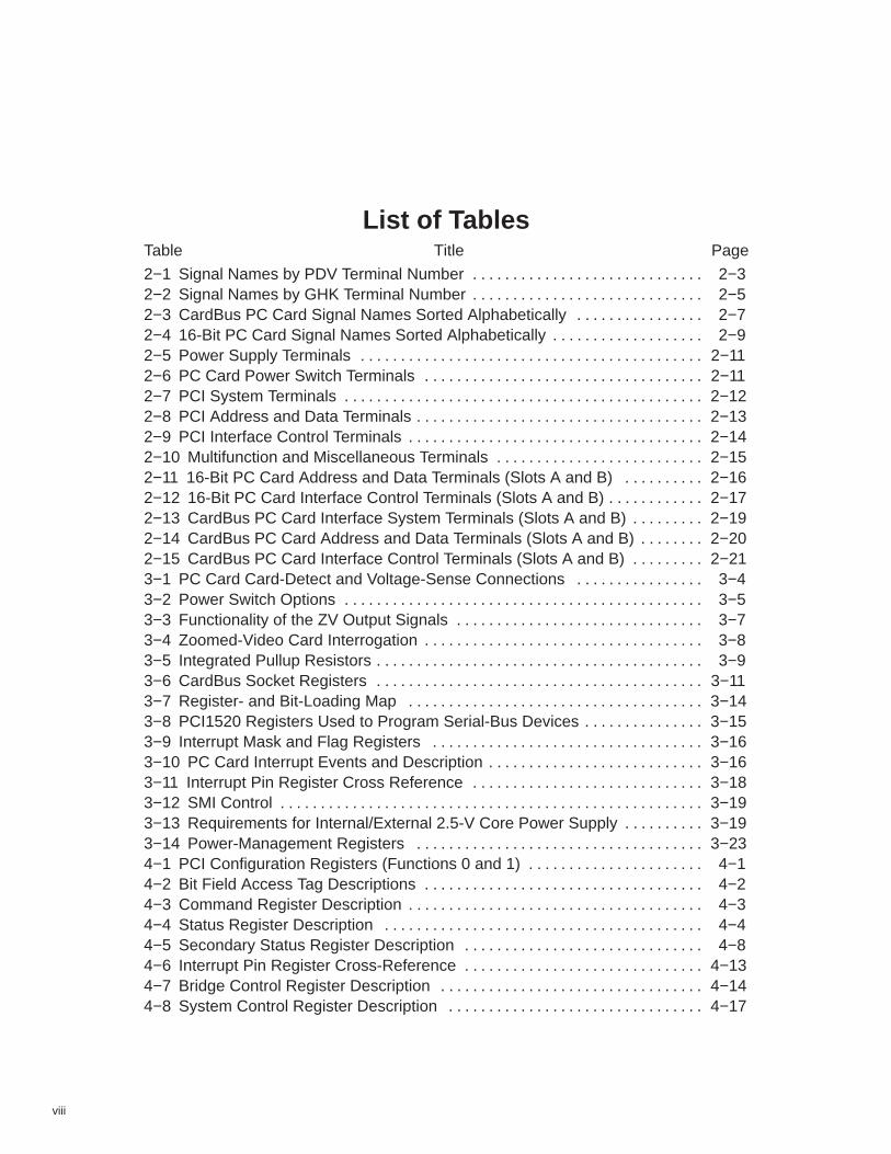
List of TablesTable Title Page
2−1 Signal Names by PDV Terminal Number 2−3. . . . . . . . . . . . . . . . . . . . . . . . . . . . . 2−2 Signal Names by GHK Terminal Number 2−5. . . . . . . . . . . . . . . . . . . . . . . . . . . . . 2−3 CardBus PC Card Signal Names Sorted Alphabetically 2−7. . . . . . . . . . . . . . . . 2−4 16-Bit PC Card Signal Names Sorted Alphabetically 2−9. . . . . . . . . . . . . . . . . . . 2−5 Power Supply Terminals 2−11. . . . . . . . . . . . . . . . . . . . . . . . . . . . . . . . . . . . . . . . . . . 2−6 PC Card Power Switch Terminals 2−11. . . . . . . . . . . . . . . . . . . . . . . . . . . . . . . . . . . 2−7 PCI System Terminals 2−12. . . . . . . . . . . . . . . . . . . . . . . . . . . . . . . . . . . . . . . . . . . . . 2−8 PCI Address and Data Terminals 2−13. . . . . . . . . . . . . . . . . . . . . . . . . . . . . . . . . . . . 2−9 PCI Interface Control Terminals 2−14. . . . . . . . . . . . . . . . . . . . . . . . . . . . . . . . . . . . . 2−10 Multifunction and Miscellaneous Terminals 2−15. . . . . . . . . . . . . . . . . . . . . . . . . . 2−11 16-Bit PC Card Address and Data Terminals (Slots A and B) 2−16. . . . . . . . . . 2−12 16-Bit PC Card Interface Control Terminals (Slots A and B) 2−17. . . . . . . . . . . . 2−13 CardBus PC Card Interface System Terminals (Slots A and B) 2−19. . . . . . . . . 2−14 CardBus PC Card Address and Data Terminals (Slots A and B) 2−20. . . . . . . . 2−15 CardBus PC Card Interface Control Terminals (Slots A and B) 2−21. . . . . . . . . 3−1 PC Card Card-Detect and Voltage-Sense Connections 3−4. . . . . . . . . . . . . . . . 3−2 Power Switch Options 3−5. . . . . . . . . . . . . . . . . . . . . . . . . . . . . . . . . . . . . . . . . . . . . 3−3 Functionality of the ZV Output Signals 3−7. . . . . . . . . . . . . . . . . . . . . . . . . . . . . . . 3−4 Zoomed-Video Card Interrogation 3−8. . . . . . . . . . . . . . . . . . . . . . . . . . . . . . . . . . . 3−5 Integrated Pullup Resistors 3−9. . . . . . . . . . . . . . . . . . . . . . . . . . . . . . . . . . . . . . . . . 3−6 CardBus Socket Registers 3−11. . . . . . . . . . . . . . . . . . . . . . . . . . . . . . . . . . . . . . . . . 3−7 Register- and Bit-Loading Map 3−14. . . . . . . . . . . . . . . . . . . . . . . . . . . . . . . . . . . . . 3−8 PCI1520 Registers Used to Program Serial-Bus Devices 3−15. . . . . . . . . . . . . . . 3−9 Interrupt Mask and Flag Registers 3−16. . . . . . . . . . . . . . . . . . . . . . . . . . . . . . . . . . 3−10 PC Card Interrupt Events and Description 3−16. . . . . . . . . . . . . . . . . . . . . . . . . . . 3−11 Interrupt Pin Register Cross Reference 3−18. . . . . . . . . . . . . . . . . . . . . . . . . . . . . 3−12 SMI Control 3−19. . . . . . . . . . . . . . . . . . . . . . . . . . . . . . . . . . . . . . . . . . . . . . . . . . . . . 3−13 Requirements for Internal/External 2.5-V Core Power Supply 3−19. . . . . . . . . . 3−14 Power-Management Registers 3−23. . . . . . . . . . . . . . . . . . . . . . . . . . . . . . . . . . . . 4−1 PCI Configuration Registers (Functions 0 and 1) 4−1. . . . . . . . . . . . . . . . . . . . . . 4−2 Bit Field Access Tag Descriptions 4−2. . . . . . . . . . . . . . . . . . . . . . . . . . . . . . . . . . . 4−3 Command Register Description 4−3. . . . . . . . . . . . . . . . . . . . . . . . . . . . . . . . . . . . . 4−4 Status Register Description 4−4. . . . . . . . . . . . . . . . . . . . . . . . . . . . . . . . . . . . . . . . 4−5 Secondary Status Register Description 4−8. . . . . . . . . . . . . . . . . . . . . . . . . . . . . . 4−6 Interrupt Pin Register Cross-Reference 4−13. . . . . . . . . . . . . . . . . . . . . . . . . . . . . . 4−7 Bridge Control Register Description 4−14. . . . . . . . . . . . . . . . . . . . . . . . . . . . . . . . . 4−8 System Control Register Description 4−17. . . . . . . . . . . . . . . . . . . . . . . . . . . . . . . .

ix
4−9 Multifunction Routing Register Description 4−19. . . . . . . . . . . . . . . . . . . . . . . . . . . 4−10 Retry Status Register Description 4−21. . . . . . . . . . . . . . . . . . . . . . . . . . . . . . . . . . 4−11 Card Control Register Description 4−22. . . . . . . . . . . . . . . . . . . . . . . . . . . . . . . . . . 4−12 Device Control Register Description 4−23. . . . . . . . . . . . . . . . . . . . . . . . . . . . . . . . 4−13 Diagnostic Register Description 4−24. . . . . . . . . . . . . . . . . . . . . . . . . . . . . . . . . . . . 4−14 Power-Management Capabilities Register Description 4−26. . . . . . . . . . . . . . . . 4−15 Power-Management Control/Status Register Description 4−27. . . . . . . . . . . . . . 4−16 Power-Management Control/Status Register Bridge Support
Extensions Description 4−28. . . . . . . . . . . . . . . . . . . . . . . . . . . . . . . . . . . . . . . . . . 4−17 General-Purpose Event Status Register Description 4−29. . . . . . . . . . . . . . . . . . 4−18 General-Purpose Event Enable Register Description 4−30. . . . . . . . . . . . . . . . . 4−19 General-Purpose Input Register Description 4−31. . . . . . . . . . . . . . . . . . . . . . . . . 4−20 General-Purpose Output Register Description 4−32. . . . . . . . . . . . . . . . . . . . . . . 4−21 Serial-Bus Data Register Description 4−32. . . . . . . . . . . . . . . . . . . . . . . . . . . . . . . 4−22 Serial-Bus Index Register Description 4−33. . . . . . . . . . . . . . . . . . . . . . . . . . . . . . 4−23 Serial-Bus Slave Address Register Description 4−33. . . . . . . . . . . . . . . . . . . . . . 4−24 Serial-Bus Control and Status Register Description 4−34. . . . . . . . . . . . . . . . . . . 5−1 ExCA Registers and Offsets 5−3. . . . . . . . . . . . . . . . . . . . . . . . . . . . . . . . . . . . . . . . 5−2 ExCA Identification and Revision Register Description 5−5. . . . . . . . . . . . . . . . . 5−3 ExCA Interface Status Register Description 5−6. . . . . . . . . . . . . . . . . . . . . . . . . . 5−4 ExCA Power Control Register Description—82365SL Support 5−7. . . . . . . . . . 5−5 ExCA Power Control Register Description—82365SL-DF Support 5−7. . . . . . . 5−6 ExCA Interrupt and General Control Register Description 5−8. . . . . . . . . . . . . . 5−7 ExCA Card Status-Change Register Description 5−9. . . . . . . . . . . . . . . . . . . . . . 5−8 ExCA Card Status-Change Interrupt Configuration
Register Description 5−10. . . . . . . . . . . . . . . . . . . . . . . . . . . . . . . . . . . . . . . . . . . . 5−9 ExCA Address Window Enable Register Description 5−11. . . . . . . . . . . . . . . . . . . 5−10 ExCA I/O Window Control Register Description 5−12. . . . . . . . . . . . . . . . . . . . . . 5−11 ExCA Memory Windows 0−4 Start-Address High-Byte Registers
Description 5−16. . . . . . . . . . . . . . . . . . . . . . . . . . . . . . . . . . . . . . . . . . . . . . . . . . . . 5−12 ExCA Memory Windows 0−4 End-Address High-Byte Registers
Description 5−18. . . . . . . . . . . . . . . . . . . . . . . . . . . . . . . . . . . . . . . . . . . . . . . . . . . . 5−13 ExCA Memory Windows 0−4 Offset-Address High-Byte Registers
Description 5−20. . . . . . . . . . . . . . . . . . . . . . . . . . . . . . . . . . . . . . . . . . . . . . . . . . . . 5−14 ExCA Card Detect and General Control Register Description 5−21. . . . . . . . . . 5−15 ExCA Global Control Register Description 5−22. . . . . . . . . . . . . . . . . . . . . . . . . . 6−1 CardBus Socket Registers 6−1. . . . . . . . . . . . . . . . . . . . . . . . . . . . . . . . . . . . . . . . . 6−2 Socket Event Register Description 6−2. . . . . . . . . . . . . . . . . . . . . . . . . . . . . . . . . . 6−3 Socket Mask Register Description 6−3. . . . . . . . . . . . . . . . . . . . . . . . . . . . . . . . . . . 6−4 Socket Present-State Register Description 6−4. . . . . . . . . . . . . . . . . . . . . . . . . . . 6−5 Socket Force Event Register Description 6−7. . . . . . . . . . . . . . . . . . . . . . . . . . . . . 6−6 Socket Control Register Description 6−8. . . . . . . . . . . . . . . . . . . . . . . . . . . . . . . . . 6−7 Socket Power-Management Register Description 6−9. . . . . . . . . . . . . . . . . . . . .

x
1−1
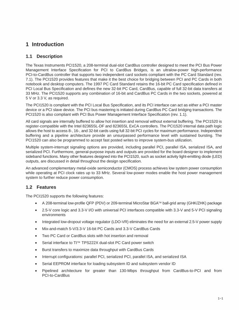
1 Introduction
1.1 Description
The Texas Instruments PCI1520, a 208-terminal dual-slot CardBus controller designed to meet the PCI Bus PowerManagement Interface Specification for PCI to CardBus Bridges, is an ultralow-power high-performancePCI-to-CardBus controller that supports two independent card sockets compliant with the PC Card Standard (rev.7.1). The PCI1520 provides features that make it the best choice for bridging between PCI and PC Cards in bothnotebook and desktop computers. The 1997 PC Card Standard retains the 16-bit PC Card specification defined inPCI Local Bus Specification and defines the new 32-bit PC Card, CardBus, capable of full 32-bit data transfers at33 MHz. The PCI1520 supports any combination of 16-bit and CardBus PC Cards in the two sockets, powered at5 V or 3.3 V, as required.
The PCI1520 is compliant with the PCI Local Bus Specification, and its PCI interface can act as either a PCI masterdevice or a PCI slave device. The PCI bus mastering is initiated during CardBus PC Card bridging transactions. ThePCI1520 is also compliant with PCI Bus Power Management Interface Specification (rev. 1.1).
All card signals are internally buffered to allow hot insertion and removal without external buffering. The PCI1520 isregister-compatible with the Intel 82365SL-DF and 82365SL ExCA controllers. The PCI1520 internal data path logicallows the host to access 8-, 16-, and 32-bit cards using full 32-bit PCI cycles for maximum performance. Independentbuffering and a pipeline architecture provide an unsurpassed performance level with sustained bursting. ThePCI1520 can also be programmed to accept fast posted writes to improve system-bus utilization.
Multiple system-interrupt signaling options are provided, including parallel PCI, parallel ISA, serialized ISA, andserialized PCI. Furthermore, general-purpose inputs and outputs are provided for the board designer to implementsideband functions. Many other features designed into the PCI1520, such as socket activity light-emitting diode (LED)outputs, are discussed in detail throughout the design specification.
An advanced complementary metal-oxide semiconductor (CMOS) process achieves low system power consumptionwhile operating at PCI clock rates up to 33 MHz. Several low-power modes enable the host power managementsystem to further reduce power consumption.
1.2 Features
The PCI1520 supports the following features:
• A 208-terminal low-profile QFP (PDV) or 209-terminal MicroStar BGA ball-grid array (GHK/ZHK) package
• 2.5-V core logic and 3.3-V I/O with universal PCI interfaces compatible with 3.3-V and 5-V PCI signalingenvironments
• Integrated low-dropout voltage regulator (LDO-VR) eliminates the need for an external 2.5-V power supply
• Mix-and-match 5-V/3.3-V 16-bit PC Cards and 3.3-V CardBus Cards
• Two PC Card or CardBus slots with hot insertion and removal
• Serial interface to TI TPS222X dual-slot PC Card power switch
• Burst transfers to maximize data throughput with CardBus Cards
• Interrupt configurations: parallel PCI, serialized PCI, parallel ISA, and serialized ISA
• Serial EEPROM interface for loading subsystem ID and subsystem vendor ID
• Pipelined architecture for greater than 130-Mbps throughput from CardBus-to-PCI and fromPCI-to-CardBus

1−2
• Up to five general-purpose I/Os
• Programmable output select for CLKRUN
• Multifunction PCI device with separate configuration space for each socket
• Five PCI memory windows and two I/O windows available for each 16-bit interface
• Two I/O windows and two memory windows available to each CardBus socket
• Exchangeable-card-architecture- (ExCA-) compatible registers are mapped in memory and I/O space
• Intel 82365SL-DF and 82365SL register compatible
• Ring indicate, SUSPEND, PCI CLKRUN, and CardBus CCLKRUN
• Socket activity LED terminals
• PCI bus lock (LOCK)
• Advanced quarter-micron, ultralow-power CMOS technology
• Internal ring oscillator
1.3 Related Documents
• Advanced Configuration and Power Interface (ACPI) Specification (revision 1.1)
• PCI Bus Power Management Interface Specification (revision 1.1)
• PCI Bus Power Management Interface Specification for PCI to CardBus Bridges (revision 0.6)
• PCI to PCMCIA CardBus Bridge Register Description (Yenta) (revision 2.1)
• PCI Local Bus Specification (revision 2.2)
• PCI Mobile Design Guide (revision 1.0)
• PC Card Standard (revision 7.1)
• PC 2001
• Serialized IRQ Support for PCI Systems (revision 6)
1.4 Trademarks
Intel is a trademark of Intel Corporation.
TI and MicroStar BGA are trademarks of Texas Instruments.
Other trademarks are the property of their respective owners.
1.5 Ordering Information
ORDERING NUMBER NAME VOLTAGE PACKAGE
PCI1520 PC Card controller 3.3 V, 5-V tolerant I/Os 208-terminal LQFP209-ball PBGA
PCI1520I PC Card controller, industrial temperature
3.3 V, 5-V tolerant I/Os 208-terminal LQFP209-ball PBGA

1−3
1.6 PCI1520 Data Manual Document History
DATE PAGE NUMBER REVISION
01/2003 2−1 Corrected part number typo in the first sentence of the page
01/2003 2−15 Corrected description of EEPROM detection scheme. EEPROM detection happens ondeassertion of GRST rather than PRST.
01/2003 3−2 Added new subsection 3.4.1 to describe GRST during power up
12/2003 3−3 Corrected bit description of SUBSYSRW bit in the system control register
01/2003 3−13 Modified byte-read diagram (Figure 3−12) to better reflect a read transaction to the EEPROM
01/2003 3−23 Modified description of power management capabilities register. This register is not a staticread-only register.
01/2003 4−13 Corrected default value for interrupt pin register
01/2003 4−26 Corrected default value for power management capabilities register
01/2003 5−13 Corrected typo on register description for ExCA I/O windows 0 and 1 start-address high-byteregister
01/2003 5−24 Corrected typo on the bit type for ExCA memory 0−4 page register
01/2003 6−8 Corrected default value for socket control register
01/2003 6−8 Modified description for bit 10 in the socket control register
03/2004 Cover Added ZHK package to document title
03/2004 1−1 Added ZHK package to text
03/2004 2−1 Added ZHK package to text
03/2004 8−1 Added ZHK package to text
03/2004 8−2 Added ZHK mechanical

1−4

2−1
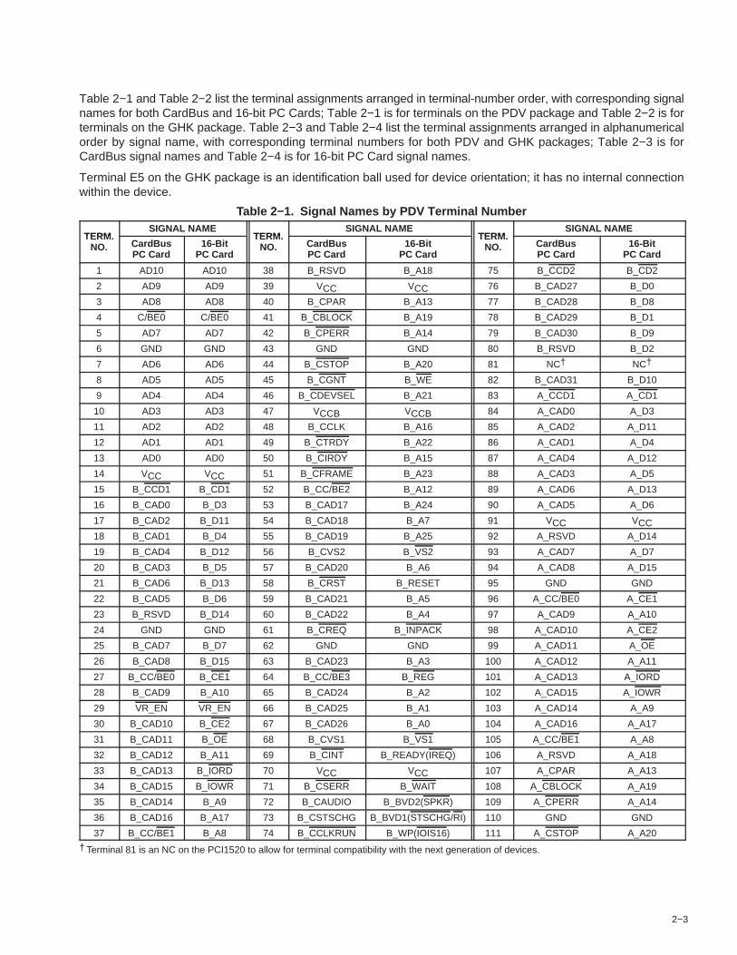
2 Terminal Descriptions
The PCI1520 is available in three packages, a 208-terminal quad flatpack (PDV) and two 209-terminal MicroStarBGA packages (GHK/ZHK). The GHK and ZHK packages are mechanically and electrically identical, but the ZHKis a lead-free (Pb, atomic number 82) design. Throughout the remainder of this manual (except Chapter 8), only theGHK designator is used for either the GHK or ZHK package. The terminal layout for the GHK package is shown inFigure 2−1. The terminal layout with signal names for the PDV package is shown in Figure 2−2.
GHK PLASTIC BALL GRID ARRAY (PBGA) PACKAGEBOTTOM VIEW
19171613 14 1511 1298 10
V
U
W
R
N
P
L
M
K
T
75 63 4
H
F
G
E
C
D
1
A
B
2
J
18
Figure 2−1. PCI1520 GHK-Package Terminal Diagram

2−2
AD
101
AD
92
AD
83
C/B
E0
4
AD
75
GN
D6
AD
67
AD
58
AD
49
AD
310
AD
211
AD
112
AD
013
VC
C14
B_C
CD
1 //B
_CD
115
B_C
AD
0//B
_D3
16
B_C
AD
2//B
_D11
17
B_C
AD
1//B
_D4
18
B_C
AD
4//B
_D12
19
B_C
AD
3//B
_D5
20
B_C
AD
6//B
_D13
21
B_C
AD
5//B
_D6
22
B_R
SV
D//B
_D14
23
GN
D24
B_C
AD
7//B
_D7
25
B_C
AD
8//B
_D15
26
B_C
C/B
E0 /
/B_C
E1
27
B_C
AD
9//B
_A10
28
VR
_EN
29
B_C
AD
10//B
_CE
230
B_C
AD
11//B
_OE
31
B_C
AD
12//B
_A11
32
B_C
AD
13//B
_IO
RD
33
B_C
AD
15//B
_IO
WR
34
B_C
AD
14//B
_A9
35
B_C
AD
16//B
_A17
36
B_C
C/B
E1 /
/B_A
837
B_R
SV
D//B
_A18
38
VC
C39
B_C
PA
R//B
_A13
40
B_C
BLO
CK
//B_A
1941
B_C
PE
RR
//B_A
1442
GN
D43
B_C
ST
OP
//B_A
2044
B_C
GN
T//B
_WE
45
B_C
DE
VS
EL /
/B_A
2146
VC
CB
47
B_C
CLK
//B_A
1648
B_C
TR
DY
//B_A
2249
B_C
IRD
Y//B
_A15
50
B_C
FR
AM
E//B
_A23
51
B_C
C/B
E2 /
/B_A
1252
104 A_CAD16//A_A17
103 A_CAD14//A_A9
102 A_CAD15//A_IOWR
101 A_CAD13//A_IORD
100 A_CAD12//A_A11
99 A_CAD11//A_OE
98 A_CAD10//A_CE2
97 A_CAD9//A_A10
96 A_CC/BE0//A_CE1
95 GND
94 A_CAD8//A_D15
93 A_CAD7//A_D7
92 A_RSVD//A_D14
91 VCC
90 A_CAD5//A_D6
89 A_CAD6//A_D13
88 A_CAD3//A_D5
87 A_CAD4//A_D12
86 A_CAD1//A_D4
85 A_CAD2//A_D11
84 A_CAD0//A_D3
83 A_CCD1//A_CD1
82 B_CAD31//B_D10
81 NC
80 B_RSVD//B_D2
79 B_CAD30//B_D9
78 B_CAD29//B_D1
77
76 B_CAD27//B_D0
75 B_CCD2//B_CD2
74 B_CCLKRUN//B_WP(IOIS16)
73 B_CSTSCHG//B_BVD1(STSCHG/RI)
72 B_CAUDIO//B_BVD2(SPKR)
71 B_CSERR//B_WAIT
70 VCC
B_CAD28//B_D8
69 B_CINT//B_READY(IREQ)
68 B_CVS1//B_VS1
67
66 B_CAD25//B_A1
65 B_CAD24//B_A2
64 B_CC/BE3//B_REG
63 B_CAD23//B_A3
62 GND
61 B_CREQ//B_INPACK
60 B_CAD22//B_A4
B_CAD26//B_A0
59 B_CAD21//B_A5
58 B_CRST//B_RESET
57
56 B_CVS2//B_VS2
55 B_CAD19//B_A25
54 B_CAD18//B_A7
53 B_CAD17//B_A24
B_CAD20//B_A6
156
MF
UN
C0
155
DA
TA
154
CLO
CK
153
LAT
CH
152
SP
KR
OU
T
151
A_C
AD
31//A
_D10
150
A_R
SV
D//A
_D2
149
A_C
AD
30//A
_D9
148
A_C
AD
29//A
_D1
147
GN
D
146
A_C
AD
28//A
_D8
145
A_C
AD
27//A
_D0
144
A_C
CD
2 //A
_CD
2
143
VC
C
142
A_C
CLK
RU
N//A
_WP
(IO
IS16
)
141
A_C
ST
SC
HG
//A_B
VD
1(S
TS
CH
G/R
I)
140
A_C
AU
DIO
//A_B
VD
2(S
PK
R)
139
A_C
SE
RR
//A_W
AIT
138
A_C
INT
//A_R
EA
DY
(IR
EQ
)
137
A_C
VS
1//A
_VS
1
136
A_C
AD
26//A
_A0
135
A_C
AD
25//A
_A1
134
A_C
AD
24//A
_A2
133
VC
C
132
A_C
C/B
E3/
/A_R
EG
131
A_C
AD
23//A
_A3
130
A_C
RE
Q//A
_IN
PA
CK
129
128
VR
_PO
RT
127
A_C
AD
21//A
_A5
126
A_C
RS
T//A
_RE
SE
T
125
A_C
AD
20//A
_A6
124
A_C
VS
2//A
_VS
2
123
A_C
AD
19//A
_A25
122
A_C
AD
18//A
_A7
A_C
AD
22//A
_A4
121
A_C
AD
17//A
_A24
120
A_C
C/B
E2 /
/A_A
12
119
118
VC
C
117
A_C
IRD
Y//A
_A15
116
A_C
TR
DY
//A_A
22
115
A_C
CLK
//A_A
16
114
VC
CA
113
A_C
DE
VS
EL/
/A_A
21
112
A_C
GN
T//A
_WE
A_C
FR
AM
E//A
_A23
111
A_C
ST
OP
//A_A
20
110
GN
D
109
108
A_C
BLO
CK
//A_A
19
107
A_C
PA
R//A
_A13
106
A_R
SV
D//A
_A18
105
A_C
C/B
E1 /
/A_A
8
A_C
PE
RR
//A_A
14
MFUNC1 157
SUSPEND 158
MFUNC2 159
MFUNC3/IRQSER 160
MFUNC4 161
MFUNC5 162
MFUNC6/CLKRUN 163
C/BE3 164
RI_OUT/PME 165
GND 166
AD25 167
PRST 168
GNT 169
REQ 170
AD31 171
AD30 172
AD11 173
VCC 174
AD29 175
AD28 176
GRST 177
AD27 178
AD26 179
VCCP 180
AD24 181
PCLK 182
IDSEL 183
AD23 184
GND 185
AD22 186
AD21 187
AD20 188
AD19 189
AD18 190
AD17 191
AD16 192
C/BE2 193
FRAME 194
VCC 195
IRDY 196
TRDY 197
DEVSEL 198
GND 199
STOP 200
PERR 201
SERR 202
PAR 203
C/BE1 204
AD15 205
AD14 206
AD13 207
AD12 208
PCI1520
PDV LOW-PROFILE QUAD FLAT PACKAGE(LQFP)
TOP VIEW
Figure 2−2. PCI1520 PDV-Package Terminal Diagram
2−3
Table 2−1 and Table 2−2 list the terminal assignments arranged in terminal-number order, with corresponding signalnames for both CardBus and 16-bit PC Cards; Table 2−1 is for terminals on the PDV package and Table 2−2 is forterminals on the GHK package. Table 2−3 and Table 2−4 list the terminal assignments arranged in alphanumericalorder by signal name, with corresponding terminal numbers for both PDV and GHK packages; Table 2−3 is forCardBus signal names and Table 2−4 is for 16-bit PC Card signal names.
Terminal E5 on the GHK package is an identification ball used for device orientation; it has no internal connectionwithin the device.
Table 2−1. Signal Names by PDV Terminal Number
TERM.SIGNAL NAME
TERM.SIGNAL NAME
TERM.SIGNAL NAME
TERM.NO. CardBus
PC Card16-Bit
PC Card
TERM.NO. CardBus
PC Card16-Bit
PC Card
TERM.NO. CardBus
PC Card16-Bit
PC Card
1 AD10 AD10 38 B_RSVD B_A18 75 B_CCD2 B_CD2
2 AD9 AD9 39 VCC VCC 76 B_CAD27 B_D0
3 AD8 AD8 40 B_CPAR B_A13 77 B_CAD28 B_D8
4 C/BE0 C/BE0 41 B_CBLOCK B_A19 78 B_CAD29 B_D1
5 AD7 AD7 42 B_CPERR B_A14 79 B_CAD30 B_D9
6 GND GND 43 GND GND 80 B_RSVD B_D2
7 AD6 AD6 44 B_CSTOP B_A20 81 NC† NC†
8 AD5 AD5 45 B_CGNT B_WE 82 B_CAD31 B_D10
9 AD4 AD4 46 B_CDEVSEL B_A21 83 A_CCD1 A_CD1
10 AD3 AD3 47 VCCB VCCB 84 A_CAD0 A_D3
11 AD2 AD2 48 B_CCLK B_A16 85 A_CAD2 A_D11
12 AD1 AD1 49 B_CTRDY B_A22 86 A_CAD1 A_D4
13 AD0 AD0 50 B_CIRDY B_A15 87 A_CAD4 A_D12
14 VCC VCC 51 B_CFRAME B_A23 88 A_CAD3 A_D5
15 B_CCD1 B_CD1 52 B_CC/BE2 B_A12 89 A_CAD6 A_D13
16 B_CAD0 B_D3 53 B_CAD17 B_A24 90 A_CAD5 A_D6
17 B_CAD2 B_D11 54 B_CAD18 B_A7 91 VCC VCC18 B_CAD1 B_D4 55 B_CAD19 B_A25 92 A_RSVD A_D14
19 B_CAD4 B_D12 56 B_CVS2 B_VS2 93 A_CAD7 A_D7
20 B_CAD3 B_D5 57 B_CAD20 B_A6 94 A_CAD8 A_D15
21 B_CAD6 B_D13 58 B_CRST B_RESET 95 GND GND
22 B_CAD5 B_D6 59 B_CAD21 B_A5 96 A_CC/BE0 A_CE1
23 B_RSVD B_D14 60 B_CAD22 B_A4 97 A_CAD9 A_A10
24 GND GND 61 B_CREQ B_INPACK 98 A_CAD10 A_CE2
25 B_CAD7 B_D7 62 GND GND 99 A_CAD11 A_OE
26 B_CAD8 B_D15 63 B_CAD23 B_A3 100 A_CAD12 A_A11
27 B_CC/BE0 B_CE1 64 B_CC/BE3 B_REG 101 A_CAD13 A_IORD
28 B_CAD9 B_A10 65 B_CAD24 B_A2 102 A_CAD15 A_IOWR
29 VR_EN VR_EN 66 B_CAD25 B_A1 103 A_CAD14 A_A9
30 B_CAD10 B_CE2 67 B_CAD26 B_A0 104 A_CAD16 A_A17
31 B_CAD11 B_OE 68 B_CVS1 B_VS1 105 A_CC/BE1 A_A8
32 B_CAD12 B_A11 69 B_CINT B_READY(IREQ) 106 A_RSVD A_A18
33 B_CAD13 B_IORD 70 VCC VCC 107 A_CPAR A_A13
34 B_CAD15 B_IOWR 71 B_CSERR B_WAIT 108 A_CBLOCK A_A19
35 B_CAD14 B_A9 72 B_CAUDIO B_BVD2(SPKR) 109 A_CPERR A_A14
36 B_CAD16 B_A17 73 B_CSTSCHG B_BVD1(STSCHG/RI) 110 GND GND
37 B_CC/BE1 B_A8 74 B_CCLKRUN B_WP(IOIS16) 111 A_CSTOP A_A20
† Terminal 81 is an NC on the PCI1520 to allow for terminal compatibility with the next generation of devices.

2−4
Table 2−1. Signal Names by PDV Terminal Number (Continued)
TERM.SIGNAL NAME
TERM.SIGNAL NAME
TERM.SIGNAL NAME
TERM.NO. CardBus
PC Card16-Bit
PC Card
TERM.NO. CardBus
PC Card16-Bit
PC Card
TERM.NO. CardBus
PC Card16-Bit
PC Card
112 A_CGNT A_WE 145 A_CAD27 A_D0 178 AD27 AD27
113 A_CDEVSEL A_A21 146 A_CAD28 A_D8 179 AD26 AD26
114 VCCA VCCA 147 GND GND 180 VCCP VCCP
115 A_CCLK A_A16 148 A_CAD29 A_D1 181 AD24 AD24
116 A_CTRDY A_A22 149 A_CAD30 A_D9 182 PCLK PCLK
117 A_CIRDY A_A15 150 A_RSVD A_D2 183 IDSEL IDSEL
118 VCC VCC 151 A_CAD31 A_D10 184 AD23 AD23
119 A_CFRAME A_A23 152 SPKROUT SPKROUT 185 GND GND
120 A_CC/BE2 A_A12 153 LATCH LATCH 186 AD22 AD22
121 A_CAD17 A_A24 154 CLOCK CLOCK 187 AD21 AD21
122 A_CAD18 A_A7 155 DATA DATA 188 AD20 AD20
123 A_CAD19 A_A25 156 MFUNC0 MFUNC0 189 AD19 AD19
124 A_CVS2 A_VS2 157 MFUNC1 MFUNC1 190 AD18 AD18
125 A_CAD20 A_A6 158 SUSPEND SUSPEND 191 AD17 AD17
126 A_CRST A_RESET 159 MFUNC2 MFUNC2 192 AD16 AD16
127 A_CAD21 A_A5 160 MFUNC3/IRQSER MFUNC3/IRQSER 193 C/BE2 C/BE2
128 VR_PORT VR_PORT 161 MFUNC4 MFUNC4 194 FRAME FRAME
129 A_CAD22 A_A4 162 MFUNC5 MFUNC5 195 VCC VCC
130 A_CREQ A_INPACK 163 MFUNC6/CLKRUN MFUNC6/CLKRUN 196 IRDY IRDY
131 A_CAD23 A_A3 164 C/BE3 C/BE3 197 TRDY TRDY
132 A_CC/BE3 A_REG 165 RI_OUT/PME RI_OUT/PME 198 DEVSEL DEVSEL
133 VCC VCC 166 GND GND 199 GND GND
134 A_CAD24 A_A2 167 AD25 AD25 200 STOP STOP
135 A_CAD25 A_A1 168 PRST PRST 201 PERR PERR
136 A_CAD26 A_A0 169 GNT GNT 202 SERR SERR
137 A_CVS1 A_VS1 170 REQ REQ 203 PAR PAR
138 A_CINT A_READY(IREQ) 171 AD31 AD31 204 C/BE1 C/BE1
139 A_CSERR A_WAIT 172 AD30 AD30 205 AD15 AD15
140 A_CAUDIO A_BVD2(SPKR) 173 AD11 AD11 206 AD14 AD14
141 A_CSTSCHG A_BVD1(STSCHG/RI)
174 VCC VCC 207 AD13 AD13
142 A_CCLKRUN A_WP(IOIS16) 175 AD29 AD29 208 AD12 AD12
143 VCC VCC 176 AD28 AD28
144 A_CCD2 A_CD2 177 GRST GRST

2−5
Table 2−2. Signal Names by GHK Terminal Number
TERM.SIGNAL NAME
TERM.SIGNAL NAME
TERM.SIGNAL NAME
TERM.NO. CardBus
PC Card16-Bit
PC Card
TERM.NO. CardBus
PC Card16-Bit
PC Card
TERM.NO. CardBus
PC Card16-Bit
PC Card
A04 AD12 AD12 E07 PERR PERR H06 AD2 AD2
A05 PAR PAR E08 FRAME FRAME H14 A_CSTSCHG A_BVD1(STSCHG/RI)
A06 GND GND E09 AD19 AD19 H15 A_CCLKRUN A_WP(IOIS16)
A07 VCC VCC E10 IDSEL IDSEL H17 A_CAUDIO A_BVD2(SPKR)
A08 AD18 AD18 E11 AD27 AD27 H18 A_CSERR A_WAIT
A09 GND GND E12 AD31 AD31 H19 A_CINT A_READY(IREQ)
A10 VCCP VCCP E13 RI_OUT/PME RI_OUT/PME J01 B_CAD4 B_D12
A11 AD29 AD29 E14 MFUNC2 MFUNC2 J02 B_CAD3 B_D5
A12 VCC VCC E17 DATA DATA J03 B_CAD6 B_D13
A13 REQ REQ E18 LATCH LATCH J05 B_CAD5 B_D6
A14 GND GND E19 A_CAD31 A_D10 J06 B_RSVD B_D14
A15 MFUNC5 MFUNC5 F01 AD3 AD3 J14 A_CAD26 A_A0
A16 MFUNC1 MFUNC1 F02 AD5 AD5 J15 A_CVS1 A_VS1
B05 AD15 AD15 F03 AD6 AD6 J17 A_CAD25 A_A1
B06 STOP STOP F05 AD8 AD8 J18 A_CAD24 A_A2
B07 IRDY IRDY F06 C/BE1 C/BE1 J19 VCC VCC
B08 AD17 AD17 F07 DEVSEL DEVSEL K01 GND GND
B09 AD22 AD22 F08 C/BE2 C/BE2 K02 B_CAD7 B_D7
B10 AD24 AD24 F09 AD20 AD20 K03 B_CAD8 B_D15
B11 AD28 AD28 F10 AD23 AD23 K05 B_CC/BE0 B_CE1
B12 AD11 AD11 F11 AD26 AD26 K06 B_CAD9 B_A10
B13 GNT GNT F12 AD25 AD25 K14 A_CC/BE3 A_REG
B14 C/BE3 C/BE3 F13 MFUNC3/IRQSER MFUNC3/IRQSER K15 A_CAD23 A_A3
B15 MFUNC4 MFUNC4 F14 SPKROUT SPKROUT K17 A_CREQ A_INPACK
C05 AD13 AD13 F15 CLOCK CLOCK K18 A_CAD22 A_A4
C06 SERR SERR F17 A_RSVD A_D2 K19 VR_PORT VR_PORT
C07 TRDY TRDY F18 A_CAD29 A_D1 L01 VR_EN VR_EN
C08 AD16 AD16 F19 GND GND L02 B_CAD10 B_CE2
C09 AD21 AD21 G01 VCC VCC L03 B_CAD11 B_OE
C10 PCLK PCLK G02 AD0 AD0 L05 B_CAD13 B_IORD
C11 GRST GRST G03 AD1 AD1 L06 B_CAD12 B_A11
C12 AD30 AD30 G05 AD4 AD4 L14 A_CAD21 A_A5
C13 PRST PRST G06 C/BE0 C/BE0 L15 A_CRST A_RESET
C14 MFUNC6/CLKRUN
MFUNC6/CLKRUN
G14 A_CAD28 A_D8 L17 A_CAD20 A_A6
C15 SUSPEND SUSPEND G15 A_CAD30 A_D9 L18 A_CVS2 A_VS2
D01 AD10 AD10 G17 A_CAD27 A_D0 L19 A_CAD19 A_A25
D19 MFUNC0 MFUNC0 G18 A_CCD2 A_CD2 M01 B_CAD15 B_IOWR
E01 GND GND G19 VCC VCC M02 B_CAD14 B_A9
E02 AD7 AD7 H01 B_CAD1 B_D4 M03 B_CAD16 B_A17
E03 AD9 AD9 H02 B_CAD2 B_D11 M05 B_RSVD B_A18
E05 NC NC H03 B_CAD0 B_D3 M06 B_CC/BE1 B_A8
E06 AD14 AD14 H05 B_CCD1 B_CD1 M14 A_CCLK A_A16

2−6
Table 2−2. Signal Names by GHK Terminal Number (Continued)
TERM.SIGNAL NAME
TERM.SIGNAL NAME
TERM.SIGNAL NAME
TERM.NO. CardBus
PC Card16-Bit
PC Card
TERM.NO. CardBus
PC Card16-Bit
PC Card
TERM.NO. CardBus
PC Card16-Bit
PC Card
M15 A_CFRAME A_A23 P17 A_CSTOP A_A20 U13 A_CAD7 A_D7
M17 A_CC/BE2 A_A12 P18 A_CGNT A_WE U14 A_CAD10 A_CE2
M18 A_CAD17 A_A24 P19 VCCA VCCA U15 A_CAD14 A_A9
M19 A_CAD18 A_A7 R01 VCCB VCCB V05 B_CAD20 B_A6
N01 VCC VCC R02 B_CTRDY B_A22 V06 B_CAD22 B_A4
N02 B_CPAR B_A13 R03 B_CFRAME B_A23 V07 B_CAD24 B_A2
N03 B_CBLOCK B_A19 R06 B_CAD19 B_A25 V08 B_CINT B_READY(IREQ)
N05 B_CGNT B_WE R07 B_CREQ B_INPACK V09 B_CAUDIO B_BVD2(SPKR)
N06 B_CPERR B_A14 R08 B_CAD26 B_A0 V10 B_CAD28 B_D8
N14 A_CBLOCK A_A19 R09 B_CCLKRUN B_WP(IOIS16) V11 B_CAD31 B_D10
N15 A_CDEVSEL A_A21 R10 B_CAD30 B_D9 V12 A_CAD4 A_D12
N17 A_CTRDY A_A22 R11 A_CAD2 A_D11 V13 A_RSVD A_D14
N18 A_CIRDY A_A15 R12 A_CAD5 A_D6 V14 A_CC/BE0 A_CE1
N19 VCC VCC R13 A_CAD9 A_A10 V15 A_CAD13 A_IORD
P01 GND GND R14 A_CAD15 A_IOWR W04 B_CAD17 B_A24
P02 B_CSTOP B_A20 R17 A_RSVD A_A18 W05 B_CRST B_RESET
P03 B_CDEVSEL B_A21 R18 A_CPERR A_A14 W06 GND GND
P05 B_CIRDY B_A15 R19 GND GND W07 B_CAD25 B_A1
P06 B_CCLK B_A16 T01 B_CC/BE2 B_A12 W08 VCC VCC
P07 B_CVS2 B_VS2 T19 A_CC/BE1 A_A8 W09 B_CSERR B_WAIT
P08 B_CAD23 B_A3 U05 B_CAD18 B_A7 W10 B_CAD27 B_D0
P09 B_CCD2 B_CD2 U06 B_CAD21 B_A5 W11 NC† NC†
P10 B_RSVD B_D2 U07 B_CC/BE3 B_REG W12 A_CAD1 A_D4
P11 A_CAD0 A_D3 U08 B_CVS1 B_VS1 W13 VCC VCC
P12 A_CAD6 A_D13 U09 B_CSTSCHG B_BVD1(STSCHG/RI) W14 GND GND
P13 A_CAD8 A_D15 U10 B_CAD29 B_D1 W15 A_CAD11 A_OE
P14 A_CAD12 A_A11 U11 A_CCD1 A_CD1 W16 A_CAD16 A_A17
P15 A_CPAR A_A13 U12 A_CAD3 A_D5
† Terminal W11 is an NC on the PCI1520 to allow for terminal compatibility with the next generation of devices.

2−7
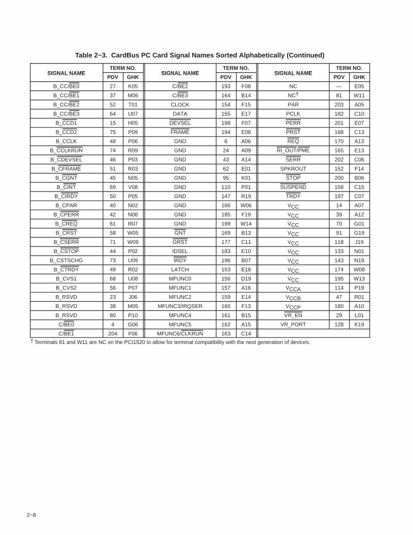
Table 2−3. CardBus PC Card Signal Names Sorted Alphabetically
SIGNAL NAMETERM NO.
SIGNAL NAMETERM. NO.
SIGNAL NAMETERM. NO.
SIGNAL NAMEPDV GHK
SIGNAL NAMEPDV GHK
SIGNAL NAMEPDV GHK
A_CAD0 84 P11 A_CDEVSEL 113 N15 AD24 181 B10
A_CAD1 86 W12 A_CFRAME 119 M15 AD25 167 F12
A_CAD2 85 R11 A_CGNT 112 P18 AD26 179 F11
A_CAD3 88 U12 A_CINT 138 H19 AD27 178 E11
A_CAD4 87 V12 A_CIRDY 117 N18 AD28 176 B11
A_CAD5 90 R12 A_CPAR 107 P15 AD29 175 A11
A_CAD6 89 P12 A_CPERR 109 R18 AD30 172 C12
A_CAD7 93 U13 A_CREQ 130 K17 AD31 171 E12
A_CAD8 94 P13 A_CRST 126 L15 B_CAD0 16 H03
A_CAD9 97 R13 A_CSERR 139 H18 B_CAD1 18 H01
A_CAD10 98 U14 A_CSTOP 111 P17 B_CAD2 17 H02
A_CAD11 99 W15 A_CSTSCHG 141 H14 B_CAD3 20 J02
A_CAD12 100 P14 A_CTRDY 116 N17 B_CAD4 19 J01
A_CAD13 101 V15 A_CVS1 137 J15 B_CAD5 22 J05
A_CAD14 103 U15 A_CVS2 124 L18 B_CAD6 21 J03
A_CAD15 102 R14 A_RSVD 106 R17 B_CAD7 25 K02
A_CAD16 104 W16 A_RSVD 92 V13 B_CAD8 26 K03
A_CAD17 121 M18 A_RSVD 150 F17 B_CAD9 28 K06
A_CAD18 122 M19 AD0 13 G02 B_CAD10 30 L02
A_CAD19 123 L19 AD1 12 G03 B_CAD11 31 L03
A_CAD20 125 L17 AD2 11 H06 B_CAD12 32 L06
A_CAD21 127 L14 AD3 10 F01 B_CAD13 33 L05
A_CAD22 129 K18 AD4 9 G05 B_CAD14 35 M02
A_CAD23 131 K15 AD5 8 F02 B_CAD15 34 M01
A_CAD24 134 J18 AD6 7 F03 B_CAD16 36 M03
A_CAD25 135 J17 AD7 5 E02 B_CAD17 53 W04
A_CAD26 136 J14 AD8 3 F05 B_CAD18 54 U05
A_CAD27 145 G17 AD9 2 E03 B_CAD19 55 R06
A_CAD28 146 G14 AD10 1 D01 B_CAD20 57 V05
A_CAD29 148 F18 AD11 173 B12 B_CAD21 59 U06
A_CAD30 149 G15 AD12 208 A04 B_CAD22 60 V06
A_CAD31 151 E19 AD13 207 C05 B_CAD23 63 P08
A_CAUDIO 140 H17 AD14 206 E06 B_CAD24 65 V07
A_CBLOCK 108 N14 AD15 205 B05 B_CAD25 66 W07
A_CC/BE0 96 V14 AD16 192 C08 B_CAD26 67 R08
A_CC/BE1 105 T19 AD17 191 B08 B_CAD27 76 W10
A_CC/BE2 120 M17 AD18 190 A08 B_CAD28 77 V10
A_CC/BE3 132 K14 AD19 189 E09 B_CAD29 78 U10
A_CCD1 83 U11 AD20 188 F09 B_CAD30 79 R10
A_CCD2 144 G18 AD21 187 C09 B_CAD31 82 V11
A_CCLK 115 M14 AD22 186 B09 B_CAUDIO 72 V09
A_CCLKRUN 142 H15 AD23 184 F10 B_CBLOCK 41 N03
2−8
Table 2−3. CardBus PC Card Signal Names Sorted Alphabetically (Continued)
SIGNAL NAMETERM NO.
SIGNAL NAMETERM NO.
SIGNAL NAMETERM NO.
SIGNAL NAMEPDV GHK
SIGNAL NAMEPDV GHK
SIGNAL NAMEPDV GHK
B_CC/BE0 27 K05 C/BE2 193 F08 NC — E05
B_CC/BE1 37 M06 C/BE3 164 B14 NC† 81 W11
B_CC/BE2 52 T01 CLOCK 154 F15 PAR 203 A05
B_CC/BE3 64 U07 DATA 155 E17 PCLK 182 C10
B_CCD1 15 H05 DEVSEL 198 F07 PERR 201 E07
B_CCD2 75 P09 FRAME 194 E08 PRST 168 C13
B_CCLK 48 P06 GND 6 A06 REQ 170 A13
B_CCLKRUN 74 R09 GND 24 A09 RI_OUT/PME 165 E13
B_CDEVSEL 46 P03 GND 43 A14 SERR 202 C06
B_CFRAME 51 R03 GND 62 E01 SPKROUT 152 F14
B_CGNT 45 N05 GND 95 K01 STOP 200 B06
B_CINT 69 V08 GND 110 P01 SUSPEND 158 C15
B_CIRDY 50 P05 GND 147 R19 TRDY 197 C07
B_CPAR 40 N02 GND 166 W06 VCC 14 A07
B_CPERR 42 N06 GND 185 F19 VCC 39 A12
B_CREQ 61 R07 GND 199 W14 VCC 70 G01
B_CRST 58 W05 GNT 169 B13 VCC 91 G19
B_CSERR 71 W09 GRST 177 C11 VCC 118 J19
B_CSTOP 44 P02 IDSEL 183 E10 VCC 133 N01
B_CSTSCHG 73 U09 IRDY 196 B07 VCC 143 N19
B_CTRDY 49 R02 LATCH 153 E18 VCC 174 W08
B_CVS1 68 U08 MFUNC0 156 D19 VCC 195 W13
B_CVS2 56 P07 MFUNC1 157 A16 VCCA 114 P19
B_RSVD 23 J06 MFUNC2 159 E14 VCCB 47 R01
B_RSVD 38 M05 MFUNC3/IRQSER 160 F13 VCCP 180 A10
B_RSVD 80 P10 MFUNC4 161 B15 VR_EN 29 L01
C/BE0 4 G06 MFUNC5 162 A15 VR_PORT 128 K19
C/BE1 204 F06 MFUNC6/CLKRUN 163 C14† Terminals 81 and W11 are NC on the PCI1520 to allow for terminal compatibility with the next generation of devices.

2−9
Table 2−4. 16-Bit PC Card Signal Names Sorted Alphabetically
SIGNAL NAMETERM. NO.
SIGNAL NAMETERM. NO.
SIGNAL NAMETERM NO.
SIGNAL NAMEPDV GHK
SIGNAL NAMEPDV GHK
SIGNAL NAMEPDV GHK
A_A0 136 J14 A_D10 151 E19 AD24 181 B10
A_A1 135 J17 A_D11 85 R11 AD25 167 F12
A_A2 134 J18 A_D12 87 V12 AD26 179 F11
A_A3 131 K15 A_D13 89 P12 AD27 178 E11
A_A4 129 K18 A_D14 92 V13 AD28 176 B11
A_A5 127 L14 A_D15 94 P13 AD29 175 A11
A_A6 125 L17 A_INPACK 130 K17 AD30 172 C12
A_A7 122 M19 A_IORD 101 V15 AD31 171 E12
A_A8 105 T19 A_IOWR 102 R14 B_A0 67 R08
A_A9 103 U15 A_OE 99 W15 B_A1 66 W07
A_A10 97 R13 A_READY(IREQ) 138 H19 B_A2 65 V07
A_A11 100 P14 A_REG 132 K14 B_A3 63 P08
A_A12 120 M17 A_RESET 126 L15 B_A4 60 V06
A_A13 107 P15 A_VS1 137 J15 B_A5 59 U06
A_A14 109 R18 A_VS2 124 L18 B_A6 57 V05
A_A15 117 N18 A_WAIT 139 H18 B_A7 54 U05
A_A16 115 M14 A_WE 112 P18 B_A8 37 M06
A_A17 104 W16 A_WP(IOIS16) 142 H15 B_A9 35 M02
A_A18 106 R17 AD0 13 G02 B_A10 28 K06
A_A19 108 N14 AD1 12 G03 B_A11 32 L06
A_A20 111 P17 AD2 11 H06 B_A12 52 T01
A_A21 113 N15 AD3 10 F01 B_A13 40 N02
A_A22 116 N17 AD4 9 G05 B_A14 42 N06
A_A23 119 M15 AD5 8 F02 B_A15 50 P05
A_A24 121 M18 AD6 7 F03 B_A16 48 P06
A_A25 123 L19 AD7 5 E02 B_A17 36 M03
A_BVD1(STSCHG/RI) 141 H14 AD8 3 F05 B_A18 38 M05
A_BVD2(SPKR) 140 H17 AD9 2 E03 B_A19 41 N03
A_CD1 83 U11 AD10 1 D01 B_A20 44 P02
A_CD2 144 G18 AD11 173 B12 B_A21 46 P03
A_CE1 96 V14 AD12 208 A04 B_A22 49 R02
A_CE2 98 U14 AD13 207 C05 B_A23 51 R03
A_D0 145 G17 AD14 206 E06 B_A24 53 W04
A_D1 148 F18 AD15 205 B05 B_A25 55 R06
A_D2 150 F17 AD16 192 C08 B_BVD1(STSCHG/RI) 73 U09
A_D3 84 P11 AD17 191 B08 B_BVD2(SPKR) 72 V09
A_D4 86 W12 AD18 190 A08 B_CD1 15 H05
A_D5 88 U12 AD19 189 E09 B_CD2 75 P09
A_D6 90 R12 AD20 188 F09 B_CE1 27 K05
A_D7 93 U13 AD21 187 C09 B_CE2 30 L02
A_D8 146 G14 AD22 186 B09 B_D0 76 W10
A_D9 149 G15 AD23 184 F10 B_D1 78 U10

2−10
Table 2−4. 16-Bit PC Card Signal Names Sorted Alphabetically (Continued)
SIGNAL NAMETERM NO.
SIGNAL NAMETERM NO.
SIGNAL NAMETERM NO.
SIGNAL NAMEPDV GHK
SIGNAL NAMEPDV GHK
SIGNAL NAMEPDV GHK
B_D2 80 P10 C/BE2 193 F08 NC — E05
B_D3 16 H03 C/BE3 164 B14 NC† 81 W11
B_D4 18 H01 CLOCK 154 F15 PAR 203 A05
B_D5 20 J02 DATA 155 E17 PCLK 182 C10
B_D6 22 J05 DEVSEL 198 F07 PERR 201 E07
B_D7 25 K02 FRAME 194 E08 PRST 168 C13
B_D8 77 V10 GND 6 A06 REQ 170 A13
B_D9 79 R10 GND 24 A09 RI_OUT/PME 165 E13
B_D10 82 V11 GND 43 A14 SERR 202 C06
B_D11 17 H02 GND 62 E01 SPKROUT 152 F14
B_D12 19 J01 GND 95 K01 STOP 200 B06
B_D13 21 J03 GND 110 P01 SUSPEND 158 C15
B_D14 23 J06 GND 147 R19 TRDY 197 C07
B_D15 26 K03 GND 166 W06 VCC 14 A07
B_INPACK 61 R07 GND 185 F19 VCC 39 A12
B_IORD 33 L05 GND 199 W14 VCC 70 G01
B_IOWR 34 M01 GNT 169 B13 VCC 91 G19
B_OE 31 L03 GRST 177 C11 VCC 118 J19
B_READY(IREQ) 69 V08 IDSEL 183 E10 VCC 133 N01
B_REG 64 U07 IRDY 196 B07 VCC 143 N19
B_RESET 58 W05 LATCH 153 E18 VCC 174 W08
B_VS1 68 U08 MFUNC0 156 D19 VCC 195 W13
B_VS2 56 P07 MFUNC1 157 A16 VCCA 114 P19
B_WAIT 71 W09 MFUNC2 159 E14 VCCB 47 R01
B_WE 45 N05 MFUNC3/IRQSER 160 F13 VCCP 180 A10
B_WP(IOIS16) 74 R09 MFUNC4 161 B15 VR_EN 29 L01
C/BE0 4 G06 MFUNC5 162 A15 VR_PORT 128 K19
C/BE1 204 F06 MFUNC6/CLKRUN 163 C14† Terminals 81 and W11 are NC on the PCI1520 to allow for terminal compatibility with the next generation of devices.
2−11
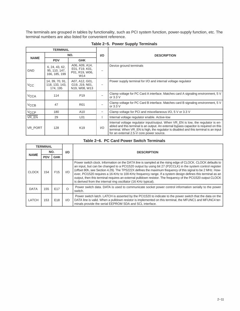
The terminals are grouped in tables by functionality, such as PCI system function, power-supply function, etc. Theterminal numbers are also listed for convenient reference.
Table 2−5. Power Supply TerminalsTERMINAL
NAMENO. I/O DESCRIPTION
NAMEPDV GHK
I/O DESCRIPTION
GND6, 24, 43, 62,95, 110, 147,166, 185, 199
A06, A09, A14,E01, F19, K01,P01, R19, W06,
W14
−
Device ground terminals
VCC14, 39, 70, 91,118, 133, 143,
174, 195
A07, A12, G01,G19, J19, N01,N19, W08, W13
−Power supply terminal for I/O and internal voltage regulator
VCCA 114 P19 −Clamp voltage for PC Card A interface. Matches card A signaling environment, 5 Vor 3.3 V
VCCB 47 R01 −Clamp voltage for PC Card B interface. Matches card B signaling environment, 5 Vor 3.3 V
VCCP 180 A10 − Clamp voltage for PCI and miscellaneous I/O, 5 V or 3.3 V
VR_EN 29 L01 I Internal voltage regulator enable. Active-low
VR_PORT 128 K19 I/O
Internal voltage regulator input/output. When VR_EN is low, the regulator is en-abled and this terminal is an output. An external bypass capacitor is required on thisterminal. When VR_EN is high, the regulator is disabled and this terminal is an inputfor an external 2.5-V core power source.
Table 2−6. PC Card Power Switch TerminalsTERMINAL
NAMENO. I/O DESCRIPTION
NAMEPDV GHK
I/O DESCRIPTION
CLOCK 154 F15 I/O
Power switch clock. Information on the DATA line is sampled at the rising edge of CLOCK. CLOCK defaults toan input, but can be changed to a PCI1520 output by using bit 27 (P2CCLK) in the system control register(offset 80h, see Section 4.29). The TPS222X defines the maximum frequency of this signal to be 2 MHz. How-ever, PCI1520 requires a 16-KHz to 100-KHz frequency range. If a system design defines this terminal as anoutput, then this terminal requires an external pulldown resistor. The frequency of the PCI1520 output CLOCKis derived from the internal ring oscillator (16 KHz typical).
DATA 155 E17 O Power switch data. DATA is used to communicate socket power control information serially to the powerswitch.
LATCH 153 E18 I/O Power switch latch. LATCH is asserted by the PCI1520 to indicate to the power switch that the data on theDATA line is valid. When a pulldown resistor is implemented on this terminal, the MFUNC1 and MFUNC4 ter-minals provide the serial EEPROM SDA and SCL interface.

2−12
Table 2−7. PCI System TerminalsTERMINAL
NAMENO. I/O DESCRIPTION
NAMEPDV GHK
I/O DESCRIPTION
GRST 177 C11 I
Global reset. When the global reset is asserted, the GRST signal causes the PCI1520 to place all outputbuffers in a high-impedance state and reset all internal registers. When GRST is asserted, the device iscompletely in its default state. For systems that require wake-up from D3, GRST normally is asserted onlyduring initial boot. PRST should be asserted following initial boot so that PME context is retained during thetransition from D3 to D0. For systems that do not require wake-up from D3, GRST should be tied to PRST.When the SUSPEND mode is enabled, the device is protected from GRST, and the internal registers arepreserved. All outputs are placed in a high-impedance state.
PCLK 182 C10 IPCI bus clock. PCLK provides timing for all transactions on the PCI bus. All PCI signals are sampled at therising edge of PCLK.
PRST 168 C13 I
PCI reset. When the PCI bus reset is asserted, PRST causes the PCI1520 to place all output buffers in ahigh-impedance state and reset internal registers. When PRST is asserted, the device can generate the PMEsignal only if it is enabled. After PRST is deasserted, the PCI1520 is in a default state.When the SUSPEND mode is enabled, the device is protected from PRST, and the internal registers arepreserved. All outputs are placed in a high-impedance state.

2−13
Table 2−8. PCI Address and Data TerminalsTERMINAL
NAMENO. I/O DESCRIPTION
NAMEPDV GHK
I/O DESCRIPTION
AD31AD30AD29AD28AD27AD26AD25AD24AD23AD22AD21AD20AD19AD18AD17AD16AD15AD14AD13AD12AD11AD10AD9AD8AD7AD6AD5AD4AD3AD2AD1AD0
171172175176178179167181184186187188189190191192205206207208173123578910111213
E12C12A11B11E11F11F12B10F10B09C09F09E09A08B08C08B05E06C05A04B12D01E03F05E02F03F02G05F01H06G03G02
I/OPCI address/data bus. These signals make up the multiplexed PCI address and data bus on the primaryinterface. During the address phase of a primary-bus PCI cycle, AD31−AD0 contain a 32-bit address orother destination information. During the data phase, AD31−AD0 contain data.
C/BE3C/BE2C/BE1C/BE0
1641932044
B14F08F06G06
I/O
PCI-bus commands and byte enables. These signals are multiplexed on the same PCI terminals. Duringthe address phase of a primary-bus PCI cycle, C/BE3−C/BE0 define the bus command. During the dataphase, this 4-bit bus is used as byte enables. The byte enables determine which byte paths of the full 32-bitdata bus carry meaningful data. C/BE0 applies to byte 0 (AD7−AD0), C/BE1 applies to byte 1 (AD15−AD8),C/BE2 applies to byte 2 (AD23−AD16), and C/BE3 applies to byte 3 (AD31−AD24).
PAR 203 A05 I/O
PCI-bus parity. In all PCI-bus read and write cycles, the PCI1520 calculates even parity across theAD31−AD0 and C/BE3−C/BE0 buses. As an initiator during PCI cycles, the PCI1520 outputs this parityindicator with a one-PCLK delay. As a target during PCI cycles, the PCI1520 compares its calculated parityto the parity indicator of the initiator. A compare error results in the assertion of a parity error (PERR).

2−14
Table 2−9. PCI Interface Control TerminalsTERMINAL
NAMENO. I/O DESCRIPTION
NAMEPDV GHK
I/O DESCRIPTION
DEVSEL 198 F07 I/OPCI device select. The PCI1520 asserts DEVSEL to claim a PCI cycle as the target device. As a PCI initiatoron the bus, the PCI1520 monitors DEVSEL until a target responds. If no target responds before timeoutoccurs, then the PCI1520 terminates the cycle with an initiator abort.
FRAME 194 E08 I/OPCI cycle frame. FRAME is driven by the initiator of a bus cycle. FRAME is asserted to indicate that a bustransaction is beginning, and data transfers continue while this signal is asserted. When FRAME isdeasserted, the PCI bus transaction is in the final data phase.
GNT 169 B13 IPCI bus grant. GNT is driven by the PCI bus arbiter to grant the PCI1520 access to the PCI bus after thecurrent data transaction has completed. GNT may or may not follow a PCI bus request, depending on the PCIbus parking algorithm.
IDSEL 183 E10 IInitialization device select. IDSEL selects the PCI1520 during configuration space accesses. IDSEL can beconnected to one of the upper 24 PCI address lines on the PCI bus.
IRDY 196 B07 I/OPCI initiator ready. IRDY indicates the ability of the PCI bus initiator to complete the current data phase of thetransaction. A data phase is completed on a rising edge of PCLK where both IRDY and TRDY are asserted.Until IRDY and TRDY are both sampled asserted, wait states are inserted.
PERR 201 E07 I/OPCI parity error indicator. PERR is driven by a PCI device to indicate that calculated parity does not matchPAR when PERR is enabled through bit 6 of the command register (PCI offset 04h, see Section 4.4).
REQ 170 A13 O PCI bus request. REQ is asserted by the PCI1520 to request access to the PCI bus as an initiator.
SERR 202 C06 O
PCI system error. SERR is an output that is pulsed from the PCI1520 when enabled through bit 8 of thecommand register (PCI offset 04h, see Section 4.4) indicating a system error has occurred. The PCI1520need not be the target of the PCI cycle to assert this signal. When SERR is enabled in the command register,this signal also pulses, indicating that an address parity error has occurred on a CardBus interface.
STOP 200 B06 I/OPCI cycle stop signal. STOP is driven by a PCI target to request the initiator to stop the current PCI bustransaction. STOP is used for target disconnects and is commonly asserted by target devices that do notsupport burst data transfers.
TRDY 197 C07 I/OPCI target ready. TRDY indicates the ability of the primary bus target to complete the current data phase ofthe transaction. A data phase is completed on a rising edge of PCLK when both IRDY and TRDY are asserted.Until both IRDY and TRDY are asserted, wait states are inserted.

2−15
Table 2−10. Multifunction and Miscellaneous Terminals
TERMINAL
NAMENO. I/O DESCRIPTION
NAMEPDV GHK
I/O DESCRIPTION
MFUNC0 156 D19 I/OMultifunction terminal 0. MFUNC0 can be configured as parallel PCI interrupt INTA, GPI0, GPO0, socketactivity LED output, ZV switching output, CardBus audio PWM, GPE, or a parallel IRQ. SeeSection 4.30, Multifunction Routing Register, for configuration details.
MFUNC1 157 A16 I/O
Multifunction terminal 1. MFUNC1 can be configured as parallel PCI interrupt INTB, GPI1, GPO1, socketactivity LED output, ZV switching output, CardBus audio PWM, GPE, or a parallel IRQ. SeeSection 4.30, Multifunction Routing Register, for configuration details.
Serial data (SDA). When LATCH is detected low after the deassertion of GRST, the MFUNC1 terminalprovides the SDA signaling for the serial bus interface. The two-terminal serial interface loads thesubsystem identification and other register defaults from an EEPROM after a PCI reset. SeeSection 3.6.1, Serial Bus Interface Implementation, for details on other serial bus applications.
MFUNC2 159 E14 I/OMultifunction terminal 2. MFUNC2 can be configured as GPI2, GPO2, socket activity LED output, ZVswitching output, CardBus audio PWM, GPE, RI_OUT, D3_STAT, or a parallel IRQ. See Section 4.30,Multifunction Routing Register, for configuration details.
MFUNC3/IRQSER
160 F13 I/OMultifunction terminal 3. MFUNC3 can be configured as a parallel IRQ or the serialized interrupt signalIRQSER. This terminal is IRQSER by default. See Section 4.30, Multifunction Routing Register, forconfiguration details.
MFUNC4 161 B15 I/O
Multifunction terminal 4. MFUNC4 can be configured as PCI LOCK, GPI3, GPO3, socket activity LEDoutput, ZV switching output, CardBus audio PWM, GPE, D3_STAT, RI_OUT, or a parallel IRQ. SeeSection 4.30, Multifunction Routing Register, for configuration details.
Serial clock (SCL). When LATCH is detected low after the deassertion of GRST, the MFUNC4 terminalprovides the SCL signaling for the serial bus interface. The two-terminal serial interface loads thesubsystem identification and other register defaults from an EEPROM after a PCI reset. SeeSection 3.6.1, Serial Bus Interface Implementation, for details on other serial bus applications.
MFUNC5 162 A15 I/OMultifunction terminal 5. MFUNC5 can be configured as GPI4, GPO4, socket activity LED output, ZVswitching output, CardBus audio PWM, D3_STAT, GPE, or a parallel IRQ. See Section 4.30,Multifunction Routing Register, for configuration details.
MFUNC6/CLKRUN
163 C14 I/OMultifunction terminal 6. MFUNC6 can be configured as a PCI CLKRUN or a parallel IRQ. SeeSection 4.30, Multifunction Routing Register, for configuration details.
NC—81
E05W11
No connect. These terminals have no connection anywhere within the package. Terminal E05 on theGHK package is used as a key to indicate the location of the A1 corner of the BGA package. TerminalsW11 on the GHK package and 81 on the PDV package will be used as a 48-MHz clock input onfuture-generation devices.
RI_OUT/PME 165 E13 ORing indicate out and power management event output. This terminal provides an output for ring-indicateor PME signals.
SPKROUT 152 F14 OSpeaker output. SPKROUT is the output to the host system that can carry SPKR or CAUDIO throughthe PCI1520 from the PC Card interface. SPKROUT is driven as the exclusive-OR combination of cardSPKR//CAUDIO inputs.
SUSPEND 158 C15 ISuspend. SUSPEND protects the internal registers from clearing when the GRST or PRST signal isasserted. See Section 3.8.5, Suspend Mode, for details.
2−16
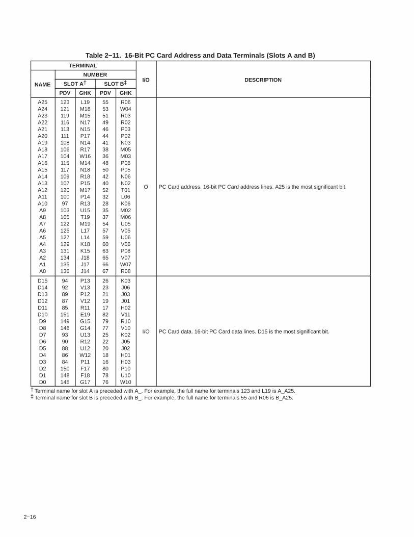
Table 2−11. 16-Bit PC Card Address and Data Terminals (Slots A and B)TERMINAL
NUMBERI/O DESCRIPTION
NAME SLOT A† SLOT B‡ I/O DESCRIPTIONNAME
PDV GHK PDV GHK
A25A24A23A22A21A20A19A18A17A16A15A14A13A12A11A10A9A8A7A6A5A4A3A2A1A0
12312111911611311110810610411511710910712010097103105122125127129131134135136
L19M18M15N17N15P17N14R17W16M14N18R18P15M17P14R13U15T19M19L17L14K18K15J18J17J14
5553514946444138364850424052322835375457596063656667
R06W04R03R02P03P02N03M05M03P06P05N06N02T01L06K06M02M06U05V05U06V06P08V07W07R08
O PC Card address. 16-bit PC Card address lines. A25 is the most significant bit.
D15D14D13D12D11D10D9D8D7D6D5D4D3D2D1D0
94928987851511491469390888684150148145
P13V13P12V12R11E19G15G14U13R12U12W12P11F17F18G17
26232119178279772522201816807876
K03J06J03J01H02V11R10V10K02J05J02H01H03P10U10W10
I/O PC Card data. 16-bit PC Card data lines. D15 is the most significant bit.
† Terminal name for slot A is preceded with A_. For example, the full name for terminals 123 and L19 is A_A25.‡ Terminal name for slot B is preceded with B_. For example, the full name for terminals 55 and R06 is B_A25.

2−17
Table 2−12. 16-Bit PC Card Interface Control Terminals (Slots A and B)TERMINAL
NUMBERI/O DESCRIPTION
NAME SLOT A† SLOT B‡ I/O DESCRIPTIONNAME
PDV GHK PDV GHK
BVD1(STSCHG/RI)
141 H14 73 U09 I
Battery voltage detect 1. BVD1 is generated by 16-bit memory PC Cards thatinclude batteries. BVD1 is used with BVD2 as an indication of the condition of thebatteries on a memory PC Card. Both BVD1 and BVD2 are high when the batteryis good. When BVD2 is low and BVD1 is high, the battery is weak and should bereplaced. When BVD1 is low, the battery is no longer serviceable and the data inthe memory PC Card is lost. See Section 5.6, ExCA Card Status-Change InterruptConfiguration Register, for enable bits. See Section 5.5, ExCA CardStatus-Change Register, and Section 5.2, ExCA Interface Status Register, for thestatus bits for this signal.
Status change. STSCHG is used to alert the system to a change in the READY,write protect, or battery voltage dead condition of a 16-bit I/O PC Card.
Ring indicate. RI is used by 16-bit modem cards to indicate a ring detection.
BVD2(SPKR)
140 H17 72 V09 I
Battery voltage detect 2. BVD2 is generated by 16-bit memory PC Cards thatinclude batteries. BVD2 is used with BVD1 as an indication of the condition of thebatteries on a memory PC Card. Both BVD1 and BVD2 are high when the batteryis good. When BVD2 is low and BVD1 is high, the battery is weak and should bereplaced. When BVD1 is low, the battery is no longer serviceable and the data inthe memory PC Card is lost. See Section 5.6, ExCA Card Status-Change InterruptConfiguration Register, for enable bits. See Section 5.5, ExCA CardStatus-Change Register, and Section 5.2, ExCA Interface Status Register, for thestatus bits for this signal.
Speaker. SPKR is an optional binary audio signal available only when the card andsocket have been configured for the 16-bit I/O interface. The audio signals fromcards A and B are combined by the PCI1520 and are output on SPKROUT.
CD1CD2
83144
U11G18
1575
H05P09
ICard detect 1 and card detect 2. CD1 and CD2 are internally connected to groundon the PC Card. When a PC Card is inserted into a socket, CD1 and CD2 are pulledlow. For signal status, see Section 5.2, ExCA Interface Status Register.
CE1CE2
9698
V14U14
2730
K05L02
OCard enable 1 and card enable 2. CE1 and CE2 enable even- and odd-numberedaddress bytes. CE1 enables even-numbered address bytes, and CE2 enablesodd-numbered address bytes.
INPACK 130 K17 61 R07 IInput acknowledge. INPACK is asserted by the PC Card when it can respond to anI/O read cycle at the current address.
IORD 101 V15 33 L05 OI/O read. IORD is asserted by the PCI1520 to enable 16-bit I/O PC Card data outputduring host I/O read cycles.
IOWR 102 R14 34 M01 OI/O write. IOWR is driven low by the PCI1520 to strobe write data into 16-bit I/O PCCards during host I/O write cycles.
† Terminal name for slot A is preceded with A_. For example, the full name for terminals 130 and K17 is A_INPACK.‡ Terminal name for slot B is preceded with B_. For example, the full name for terminals 61 and R07 is B_INPACK.

2−18
Table 2−12. 16-Bit PC Card Interface Control Terminals (Slots A and B) (Continued)TERMINAL
NUMBERI/O DESCRIPTION
NAME SLOT A† SLOT B‡ I/O DESCRIPTIONNAME
PDV GHK PDV GHK
OE 99 W15 31 L03 OOutput enable. OE is driven low by the PCI1520 to enable 16-bit memory PC Card dataoutput during host memory read cycles.
READY(IREQ)
138 H19 69 V08 I
Ready. The ready function is provided by READY when the 16-bit PC Card and the hostsocket are configured for the memory-only interface. READY is driven low by 16-bit memoryPC Cards to indicate that the memory card circuits are busy processing a previous writecommand. READY is driven high when the 16-bit memory PC Card is ready to accept a newdata transfer command.
Interrupt request. IREQ is asserted by a 16-bit I/O PC Card to indicate to the host that adevice on the 16-bit I/O PC Card requires service by the host software. IREQ is high(deasserted) when no interrupt is requested.
REG 132 K14 64 U07 O
Attribute memory select. REG remains high for all common memory accesses. When REGis asserted, access is limited to attribute memory (OE or WE active) and to the I/O space(IORD or IOWR active). Attribute memory is a separately accessed section of card memoryand is generally used to record card capacity and other configuration and attributeinformation.
RESET 126 L15 58 W05 O PC Card reset. RESET forces a hard reset to a 16-bit PC Card.
VS1VS2
137124
J15L18
6856
U08P07
I/OVoltage sense 1 and voltage sense 2. VS1 and VS2, when used in conjunction with eachother, determine the operating voltage of the PC Card.
WAIT 139 H18 71 W09 IBus cycle wait. WAIT is driven by a 16-bit PC Card to extend the completion of the memoryor I/O cycle in progress.
WE 112 P18 45 N05 OWrite enable. WE is used to strobe memory write data into 16-bit memory PC Cards. WEis also used for memory PC Cards that employ programmable memory technologies.
WP(IOIS16)
142 H15 74 R09 I
Write protect. WP applies to 16-bit memory PC Cards. WP reflects the status of thewrite-protect switch on 16-bit memory PC Cards. For 16-bit I/O cards, WP is used for the16-bit port (IOIS16) function.
I/O is 16 bits. IOIS16 applies to 16-bit I/O PC Cards. IOIS16 is asserted by the 16-bit PC Cardwhen the address on the bus corresponds to an address to which the 16-bit PC Cardresponds, and the I/O port that is addressed is capable of 16-bit accesses.
† Terminal name for slot A is preceded with A_. For example, the full name for terminals 112 and P18 is A_WE.‡ Terminal name for slot B is preceded with B_. For example, the full name for terminals 45 and N05 is B_WE.

2−19
Table 2−13. CardBus PC Card Interface System Terminals (Slots A and B)TERMINAL
NUMBERI/O DESCRIPTION
NAME SLOT A† SLOT B‡ I/O DESCRIPTIONNAME
PDV GHK PDV GHK
CCLK 115 M14 48 P06 O
CardBus clock. CCLK provides synchronous timing for all transactions on theCardBus interface. All signals except CRST, CCLKRUN, CINT, CSTSCHG, CAUDIO,CCD2, CCD1, CVS2, and CVS1 are sampled on the rising edge of CCLK, and alltiming parameters are defined with the rising edge of this signal. CCLK operates atthe PCI bus clock frequency, but it can be stopped in the low state or slowed downfor power savings.
CCLKRUN 142 H15 74 R09 I/OCardBus clock run. CCLKRUN is used by a CardBus PC Card to request an increasein the CCLK frequency, and by the PCI1520 to indicate that the CCLK frequency isgoing to be decreased.
CRST 126 L15 58 W05 O
CardBus reset. CRST brings CardBus PC Card-specific registers, sequencers, andsignals to a known state. When CRST is asserted, all CardBus PC Card signals areplaced in a high-impedance state, and the PCI1520 drives these signals to a validlogic level. Assertion can be asynchronous to CCLK, but deassertion must besynchronous to CCLK.
† Terminal name for slot A is preceded with A_. For example, the full name for terminals 115 and M14 is A_CCLK.‡ Terminal name for slot B is preceded with B_. For example, the full name for terminals 48 and P06 is B_CCLK.

2−20
Table 2−14. CardBus PC Card Address and Data Terminals (Slots A and B)TERMINAL
NUMBERI/O DESCRIPTION
NAME SLOT A† SLOT B‡ I/O DESCRIPTIONNAME
PDV GHK PDV GHK
CAD31CAD30CAD29CAD28CAD27CAD26CAD25CAD24CAD23CAD22CAD21CAD20CAD19CAD18CAD17CAD16CAD15CAD14CAD13CAD12CAD11CAD10CAD9CAD8CAD7CAD6CAD5CAD4CAD3CAD2CAD1CAD0
151149148146145136135134131129127125123122121104102103101100999897949389908788858684
E19G15F18G14G17J14J17J18K15K18L14L17L19M19M18W16R14U15V15P14W15U14R13P13U13P12R12V12U12R11W12P11
8279787776676665636059575554533634353332313028262521221920171816
V11R10U10V10W10R08W07V07P08V06U06V05R06U05W04M03M01M02L05L06L03L02K06K03K02J03J05J01J02H02H01H03
I/O
CardBus address and data. These signals make up the multiplexed CardBus addressand data bus on the CardBus interface. During the address phase of a CardBus cycle,CAD31−CAD0 contain a 32-bit address. During the data phase of a CardBus cycle,CAD31−CAD0 contain data. CAD31 is the most significant bit.
CC/BE3CC/BE2CC/BE1CC/BE0
13212010596
K14M17T19V14
64523727
U07T01M06K05
I/O
CardBus bus commands and byte enables. CC/BE3−CC/BE0 are multiplexed on thesame CardBus terminals. During the address phase of a CardBus cycle,CC/BE3−CC/BE0 define the bus command. During the data phase, this 4-bit bus is usedas byte enables. The byte enables determine which byte paths of the full 32-bit data buscarry meaningful data. CC/BE0 applies to byte 0 (CAD7−CAD0), CC/BE1 applies tobyte 1 (CAD15−CAD8), CC/BE2 applies to byte 2 (CAD23−CAD16), and CC/BE3applies to byte 3 (CAD31−CAD24).
CPAR 107 P15 40 N02 I/O
CardBus parity. In all CardBus read and write cycles, the PCI1520 calculates even parityacross the CAD and CC/BE buses. As an initiator during CardBus cycles, the PCI1520outputs CPAR with a one-CCLK delay. As a target during CardBus cycles, the PCI1520compares its calculated parity to the parity indicator of the initiator; a compare errorresults in a parity error assertion.
† Terminal name for slot A is preceded with A_. For example, the full name for terminals 107 and P15 is A_CPAR.‡ Terminal name for slot B is preceded with B_. For example, the full name for terminals 40 and N02 is B_CPAR.

2−21
Table 2−15. CardBus PC Card Interface Control Terminals (Slots A and B)
TERMINAL
NUMBERI/O DESCRIPTION
NAME SLOT A† SLOT B‡ I/O DESCRIPTIONNAME
PDV GHK PDV GHK
CAUDIO 140 H17 72 V09 ICardBus audio. CAUDIO is a digital input signal from a PC Card to the systemspeaker. The PCI1520 supports the binary audio mode and outputs a binary signalfrom the card to SPKROUT.
CBLOCK 108 N14 41 N03 I/O CardBus lock. CBLOCK is used to gain exclusive access to a target.
CCD1 83 U11 15 H05I
CardBus detect 1 and CardBus detect 2. CCD1 and CCD2 are used in conjunctionwith CVS1 and CVS2 to identify card insertion and interrogate cards to determine the
CCD1CCD2
83144
U11G18
1575
H05P09 I with CVS1 and CVS2 to identify card insertion and interrogate cards to determine the
operating voltage and card type.
CDEVSEL 113 N15 46 P03 I/O
CardBus device select. The PCI1520 asserts CDEVSEL to claim a CardBus cycle asthe target device. As a CardBus initiator on the bus, the PCI1520 monitors CDEVSELuntil a target responds. If no target responds before timeout occurs, then the PCI1520terminates the cycle with an initiator abort.
CFRAME 119 M15 51 R03 I/O
CardBus cycle frame. CFRAME is driven by the initiator of a CardBus bus cycle.CFRAME is asserted to indicate that a bus transaction is beginning, and datatransfers continue while this signal is asserted. When CFRAME is deasserted, theCardBus bus transaction is in the final data phase.
CGNT 112 P18 45 N05 OCardBus bus grant. CGNT is driven by the PCI1520 to grant a CardBus PC Cardaccess to the CardBus bus after the current data transaction has been completed.
CINT 138 H19 69 V08 ICardBus interrupt. CINT is asserted low by a CardBus PC Card to request interruptservicing from the host.
CIRDY 117 N18 50 P05 I/O
CardBus initiator ready. CIRDY indicates the ability of the CardBus initiator tocomplete the current data phase of the transaction. A data phase is completed on arising edge of CCLK when both CIRDY and CTRDY are asserted. Until CIRDY andCTRDY are both sampled asserted, wait states are inserted.
CPERR 109 R18 42 N06 I/OCardBus parity error. CPERR reports parity errors during CardBus transactions,except during special cycles. It is driven low by a target two clocks following the datacycle during which a parity error is detected.
CREQ 130 K17 61 R07 ICardBus request. CREQ indicates to the arbiter that the CardBus PC Card desiresuse of the CardBus bus as an initiator.
CSERR 139 H18 71 W09 I
CardBus system error. CSERR reports address parity errors and other system errorsthat could lead to catastrophic results. CSERR is driven by the card synchronous toCCLK, but deasserted by a weak pullup; deassertion may take several CCLK periods.The PCI1520 can report CSERR to the system by assertion of SERR on the PCIinterface.
CSTOP 111 P17 44 P02 I/OCardBus stop. CSTOP is driven by a CardBus target to request the initiator to stopthe current CardBus transaction. CSTOP is used for target disconnects, and iscommonly asserted by target devices that do not support burst data transfers.
CSTSCHG 141 H14 73 U09 ICardBus status change. CSTSCHG alerts the system to a change in the card status,and is used as a wake-up mechanism.
CTRDY 116 N17 49 R02 I/O
CardBus target ready. CTRDY indicates the ability of the CardBus target to completethe current data phase of the transaction. A data phase is completed on a rising edgeof CCLK, when both CIRDY and CTRDY are asserted; until this time, wait states areinserted.
CVS1CVS2
137124
J15L18
6856
U08P07
I/OCardBus voltage sense 1 and CardBus voltage sense 2. CVS1 and CVS2 are usedin conjunction with CCD1 and CCD2 to identify card insertion and interrogate cardsto determine the operating voltage and card type.
† Terminal name for slot A is preceded with A_. For example, the full name for terminals 140 and H18 is A_CAUDIO.‡ Terminal name for slot B is preceded with B_. For example, the full name for terminals 72 and V09 is B_CAUDIO.

2−22

3−1
3 Feature/Protocol Descriptions
The following sections give an overview of the PCI1520. Figure 3−1 shows a simplified block diagram of the PCI1520.The PCI interface includes all address/data and control signals for PCI protocol. The interrupt interface includesterminals for parallel PCI, parallel ISA, and serialized PCI and ISA signaling. Miscellaneous system interfaceterminals include multifunction terminals: SUSPEND, RI_OUT/PME (power management control signal), andSPKROUT.
PCI Bus
PCI1520
Activity LEDs
PCI950IRQSER
Deserializer
IRQSER
3
InterruptController
INTA
INTB
IRQ2−15
Multiplexer23
23
PC CardSocket A
TPS222XPower Switch 3
PC CardSocket B
External ZV Port
VGAController
AudioSubsystem
Zoomed Video
19
4
Zoomed Video
NOTE: The PC Card interface is 68 terminals for CardBus and 16-bit PC Cards. In zoomed video mode 23 terminals are used for routing thezoomed video signals to the VGA controller and audio subsystem.
68 68
68
68
23
Figure 3−1. PCI1520 Simplified Block Diagram
3.1 Power Supply Sequencing
The PCI1520 contains 3.3-V I/O buffers with 5-V tolerance requiring an I/O power supply and an LDO-VR powersupply for core logic. The core power supply, which is always 2.5 V, can be supplied through the VR_PORT terminal(when VR_EN is high) or from the integrated LDO-VR. The LDO-VR needs a 3.3-V power supply via the VCCterminals. The clamping voltages (VCCA, VCCB, and VCCP) can be either 3.3 V or 5 V, depending on the interface. Thefollowing power-up and power-down sequences are recommended.
The power-up sequence is:
1. Assert GRST to the device to disable the outputs during power up. Output drivers must be powered up inthe high-impedance state to prevent high current levels through the clamp diodes to the 5-V clamping rails(VCCA, VCCB, and VCCP).
2. Apply 3.3-V power to VCC.
3. Apply the clamp voltage.

3−2
The power-down sequence is:
1. Assert GRST to the device to disable the outputs during power down. Output drivers must be powered downin the high-impedance state to prevent high current levels through the clamp diodes to the 5-V clampingrails (VCCA, VCCB, and VCCP).
2. Remove the clamp voltage.
3. Remove the 3.3-V power from VCC.
NOTE: The clamp voltage can be ramped up or ramped down along with the 3.3-V power. Thevoltage difference between VCC and the clamp voltage must remain within 3.6 V.
3.2 I/O Characteristics
Figure 3−2 shows a 3-state bidirectional buffer. Section 7.2, Recommended Operating Conditions, provides theelectrical characteristics of the inputs and outputs.
NOTE: The PCI1520 meets the ac specifications of the 1997 PC Card Standard and PCI LocalBus Specification.
Tied for Open DrainOE
Pad
VCCP
Figure 3−2. 3-State Bidirectional Buffer
NOTE: Unused terminals (input or I/O) must be held high or low to prevent them from floating.
3.3 Clamping Voltages
The clamping voltages are set to match whatever external environment the PCI1520 is interfaced with, 3.3 V or 5 V.The I/O sites can be pulled through a clamping diode to a voltage rail that protects the core from external signals.The core power supply is always 3.3 V and is independent of the clamping voltages. For example, PCI signaling canbe either 3.3 V or 5 V, and the PCI1520 must reliably accommodate both voltage levels. This is accomplished by usinga 3.3-V I/O buffer that is 5-V tolerant, with the applicable clamping voltage applied. If a system designer desires a5-V PCI bus, then VCCP can be connected to a 5-V power supply.
The PCI1520 requires three separate clamping voltages because it supports a wide range of features. The threevoltages are listed and defined in Section 7.2, Recommended Operating Conditions. GRST, SUSPEND, PME, andCSTSCHG are not clamped to any of them.
3.4 Peripheral Component Interconnect (PCI) Interface
The PCI1520 is fully compliant with the PCI Local Bus Specification. The PCI1520 provides all required signals forPCI master or slave operation, and may operate in either a 5-V or 3.3-V signaling environment by connecting the VCCPterminal to the desired voltage level. In addition to the mandatory PCI signals, the PCI1520 provides the optionalinterrupt signals INTA and INTB.
3.4.1 PCI GRST Signal
During the power-up sequence, GRST and PRST must be asserted. GRST can only be deasserted 100 µs after PCLKis stable. PRST can be deasserted at the same time as GRST or any time thereafter.

3−3
3.4.2 PCI Bus Lock (LOCK )
The bus-locking protocol defined in the PCI Local Bus Specification is not highly recommended, but is provided onthe PCI1520 as an additional compatibility feature. The PCI LOCK signal can be routed to the MFUNC4 terminal bysetting the appropriate values in bits 19−16 of the multifunction routing register. See Section 4.30, MultifunctionRouting Register, for details. Note that the use of LOCK is only supported by PCI-to-CardBus bridges in thedownstream direction (away from the processor).
PCI LOCK indicates an atomic operation that may require multiple transactions to complete. When LOCK is asserted,nonexclusive transactions can proceed to an address that is not currently locked. A grant to start a transaction onthe PCI bus does not guarantee control of LOCK; control of LOCK is obtained under its own protocol. It is possiblefor different initiators to use the PCI bus while a single master retains ownership of LOCK. Note that the CardBussignal for this protocol is CBLOCK to avoid confusion with the bus clock.
An agent may need to do an exclusive operation because a critical access to memory might be broken into severaltransactions, but the master wants exclusive rights to a region of memory. The granularity of the lock is defined byPCI to be 16 bytes, aligned. The LOCK protocol defined by the PCI Local Bus Specification allows a resource lockwithout interfering with nonexclusive real-time data transfer, such as video.
The PCI bus arbiter may be designed to support only complete bus locks using the LOCK protocol. In this scenario,the arbiter will not grant the bus to any other agent (other than the LOCK master) while LOCK is asserted. A completebus lock may have a significant impact on the performance of the video. The arbiter that supports complete bus lockmust grant the bus to the cache to perform a writeback due to a snoop to a modified line when a locked operationis in progress.
The PCI1520 supports all LOCK protocol associated with PCI-to-PCI bridges, as also defined for PCI-to-CardBusbridges. This includes disabling write posting while a locked operation is in progress, which can solve a potentialdeadlock when using devices such as PCI-to-PCI bridges. The potential deadlock can occur if a CardBus targetsupports delayed transactions and blocks access to the target until it completes a delayed read. This targetcharacteristic is prohibited by the PCI Local Bus Specification, and the issue is resolved by the PCI master usingLOCK.
3.4.3 Loading Subsystem Identification
The subsystem vendor ID register (PCI offset 40h, see Section 4.26) and subsystem ID register (PCI offset 42h, seeSection 4.27) make up a doubleword of PCI configuration space for functions 0 and 1. This doubleword register isused for system and option card (mobile dock) identification purposes and is required by some operating systems.Implementation of this unique identifier register is a PC 99/PC 2001 requirement.
The PCI1520 offers two mechanisms to load a read-only value into the subsystem registers. The first mechanismrelies upon the system BIOS providing the subsystem ID value. The default access mode to the subsystem registersis read-only, but can be made read/write by clearing bit 5 (SUBSYSRW) in the system control register (PCI offset 80h,see Section 4.29). Once this bit is cleared, the BIOS can write a subsystem identification value into the registers atPCI offset 40h. The BIOS must set the SUBSYSRW bit such that the subsystem vendor ID register and subsystemID register is limited to read-only access. This approach saves the added cost of implementing the serial electricallyerasable programmable ROM (EEPROM).
In some conditions, such as in a docking environment, the subsystem vendor ID register and subsystem ID registermust be loaded with a unique identifier via a serial EEPROM. The PCI1520 loads the data from the serial EEPROMafter a reset of the primary bus. Note that the SUSPEND input gates the PCI reset from the entire PCI1520 core,including the serial-bus state machine (see Section 3.8.5, Suspend Mode, for details on using SUSPEND).
The PCI1520 provides a two-line serial-bus host controller that can interface to a serial EEPROM. See Section 3.6,Serial-Bus Interface, for details on the two-wire serial-bus controller and applications.

3−4
3.5 PC Card Applications
This section describes the PC Card interfaces of the PCI1520.
• Card insertion/removal and recognition• P2C power-switch interface• Zoomed video support• Speaker and audio applications• LED socket activity indicators• CardBus socket registers
3.5.1 PC Card Insertion/Removal and Recognition
The PC Card Standard (release 7.1) addresses the card-detection and recognition process through an interrogationprocedure that the socket must initiate on card insertion into a cold, nonpowered socket. Through this interrogation,card voltage requirements and interface (16-bit versus CardBus) are determined.
The scheme uses the card-detect and voltage-sense signals. The configuration of these four terminals identifies thecard type and voltage requirements of the PC Card interface. The encoding scheme is defined in the PC CardStandard (release 7.1) and in Table 3−1.
Table 3−1. PC Card Card-Detect and Voltage-Sense Connections
CD2//CCD2 CD1//CCD1 VS2//CVS2 VS1//CVS1 KEY INTERFACE VOLTAGE
Ground Ground Open Open 5 V 16-bit PC Card 5 V
Ground Ground Open Ground 5 V 16-bit PC Card 5 V and 3.3 V
Ground Ground Ground Ground 5 V 16-bit PC Card 5 V, 3.3 V, and X.X V
Ground Ground Open Ground LV 16-bit PC Card 3.3 V
Ground Connect to CVS1 Open Connect to CCD1 LV CardBus PC Card 3.3 V
Ground Ground Ground Ground LV 16-bit PC Card 3.3 V and X.X V
Connect to CVS2 Ground Connect to CCD2 Ground LV CardBus PC Card 3.3 V and X.X V
Connect to CVS1 Ground Ground Connect to CCD2 LV CardBus PC Card 3.3 V, X.X V, and Y.Y V
Ground Ground Ground Open LV 16-bit PC Card X.X V
Connect to CVS2 Ground Connect to CCD2 Open LV CardBus PC Card X.X V
Ground Connect to CVS2 Connect to CCD1 Open LV CardBus PC Card X.X V and Y.Y V
Connect to CVS1 Ground Open Connect to CCD2 LV CardBus PC Card Y.Y V
Ground Connect to CVS1 Ground Connect to CCD1 Reserved
Ground Connect to CVS2 Connect to CCD1 Ground Reserved
3.5.2 P2C Power-Switch Interface (TPS222X)
The PCI1520 provides a PCMCIA peripheral control (P2C) interface for control of the PC Card power switch. TheCLOCK, DATA, and LATCH terminals interface with the TI TPS222X dual-slot PC Card power interface switches toprovide power switch support. Figure 3−3 illustrates a typical application where the PCI1520 represents the PCMCIAcontroller. Table 3−2 shows the available power switch options compatible with the PCI1520.

3−5
PCI1520(PCMCIA
Controller)
12 V
Power Supply
VPP1VPP2VCCVCC
PC CardA
TPS222X
5 V3.3 V
CLOCK VPP1VPP2VCCVCC
PC CardB
12 V5 V3.3 V
AVPP
AVCCAVCC
BVPP
BVCCBVCCBVCC
AVCCSupervisor RESETRESET
DATALATCH
Figure 3−3. TPS222X Typical Application
Table 3−2. Power Switch OptionsDEVICE PIN-COMPATIBLE REPLACEMENT(S)
TPS2206TPS2226IDB† – 30-pin SSOPTPS2216ADAP – 32-pin TSSOP
TPS2214(A) TPS2224IDB† – 24-pin SSOP
TPS2216(A) TPS2226IDB† – 30 pin SSOP
TPS2223†‡ N/A − Check for newer device
TPS2224† N/A − Check for newer device
TPS2226† N/A − Check for newer device† Recommended for new designs‡ For applications not requiring 12 volts
The CLOCK terminal on the PCI1520 can be an input or an output. The PCI1520 defaults the CLOCK terminal asan input to control the serial interface and the internal state machine. Bit 27 (P2CCLK) in the system control register(offset 80h, see Section 4.29) can be set by the platform BIOS or the serial EEPROM to enable the PCI1520 togenerate and drive CLOCK internally from the PCI clock. When the system design implements CLOCK as an outputfrom the PCI1520, an external pulldown resistor is required.
3.5.3 Zoomed Video Support
The PCI1520 allows for the implementation of zoomed video (ZV) for PC Cards. Zoomed video is supported by settingbit 6 (ZVENABLE) in the card control register (PCI offset 91h, see Section 4.32) on a per-socket function basis.Setting this bit puts 16-bit PC Card address lines A25−A4 of the PC Card interface in the high-impedance state. Theselines can then transfer video and audio data directly to the appropriate controller. Card address lines A3−A0 can stillaccess PC Card CIS registers for PC Card configuration. Figure 3−4 illustrates a PCI1520 ZV implementation.
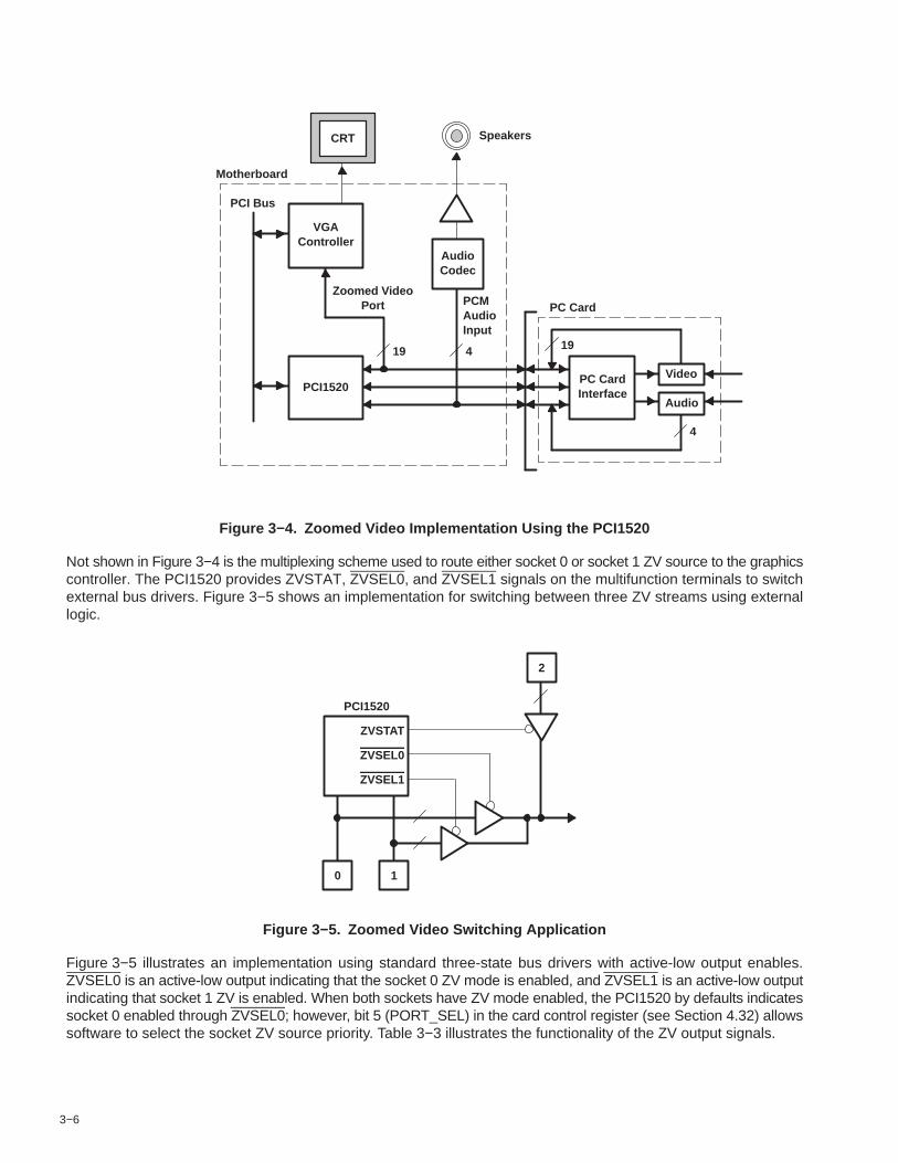
3−6
CRT
VGAController
AudioCodec
PCI1520
19 4
Zoomed VideoPort PCM
AudioInput
PCI Bus
PC CardInterface
Video
Audio
19
4
PC Card
Motherboard
Speakers
Figure 3−4. Zoomed Video Implementation Using the PCI1520
Not shown in Figure 3−4 is the multiplexing scheme used to route either socket 0 or socket 1 ZV source to the graphicscontroller. The PCI1520 provides ZVSTAT, ZVSEL0, and ZVSEL1 signals on the multifunction terminals to switchexternal bus drivers. Figure 3−5 shows an implementation for switching between three ZV streams using externallogic.
ZVSTAT
ZVSEL0
ZVSEL1
PCI1520
2
0 1
Figure 3−5. Zoomed Video Switching Application
Figure 3−5 illustrates an implementation using standard three-state bus drivers with active-low output enables.ZVSEL0 is an active-low output indicating that the socket 0 ZV mode is enabled, and ZVSEL1 is an active-low outputindicating that socket 1 ZV is enabled. When both sockets have ZV mode enabled, the PCI1520 by defaults indicatessocket 0 enabled through ZVSEL0; however, bit 5 (PORT_SEL) in the card control register (see Section 4.32) allowssoftware to select the socket ZV source priority. Table 3−3 illustrates the functionality of the ZV output signals.

3−7
Table 3−3. Functionality of the ZV Output Signals
INPUTS OUTPUTS
PORTSEL SOCKET 0 ENABLE SOCKET 1 ENABLE ZVSEL0 ZVSEL1 ZVSTAT
X 0 0 1 1 0
0 1 X 0 1 1
0 0 1 1 0 1
1 X 1 1 0 1
1 1 0 0 1 1
Also shown in Figure 3−5 is a third ZV input that can be provided from a source such as a high-speed serial bus likeIEEE 1394. The ZVSTAT signal provides a mechanism to switch the third ZV source. ZVSTAT is an active-high outputindicating that one of the PCI1520 sockets is enabled for ZV mode. The implementation shown in Figure 3−5 can beused if PC Card ZV is prioritized over other sources.
3.5.4 Standardized Zoomed-Video Register Model
The standardized zoomed-video register model is defined for the purpose of standardizing the ZV port control for PCCard controllers across the industry. The following list summarizes the standardized zoomed-video register modelchanges to the existing PC Card register set.
• Socket present state register (CardBus socket address + 08h, see Section 6.3)Bit 27 (ZVSUPPORT) has been added. The platform BIOS can set this bit via the socket force event register(CardBus socket address + 0Ch, see Section 6.4) to define whether zoomed video is supported on thatsocket by the platform.
• Socket force event register (CardBus socket address + 0Ch, see Section 6.4)Bit 27 (FZVSUPPORT) has been added. The platform BIOS can use this bit to set the ZVSUPPORT bit inthe socket present state register (CardBus socket address + 08h, see Section 6.3) to define whetherzoomed video is supported on that socket by the platform.
• Socket control register (CardBus socket address +10h, see Section 6.5)Bit 11 (ZV_ACTIVITY) has been added. This bit is set when zoomed video is enabled for either of the PCCard sockets.
Bit 10 (STDZVREG) has been added. This bit defines whether the PC Card controller supports thestandardized zoomed-video register model.
Bit 9 (ZVEN) is provided for software to enable or disable zoomed video, per socket.
If the STDZVEN bit (bit 0) in the diagnostic register (PCI offset 93h, see Section 4.34) is 1, then the standardizedzoomed video register model is disabled. For backward compatibility, even if the STDZVEN bit is 0 (enabled), thePCI1520 allows software to access zoomed video through the legacy address in the card control register (PCI offset91h, see Section 4.32), or through the new register model in the socket control register (CardBus socket address +10h, see Section 6.5).
3.5.4.1 Zoomed-Video Card Insertion and Configuration Procedure
1. A zoomed-video PC Card is inserted into an empty slot.2. The card is detected and interrogated appropriately.

3−8
There are two types of PC Card controllers to consider.
• Legacy controller not using the standardized ZV register modelSoftware reads bit 10 (STDZVREG) of the socket control register (CardBus socket address + 10h) todetermine if the standardized zoomed-video register model is supported. If the bit returns 0, then softwaremust use legacy code to enable zoomed video.
• Newer controller that uses the standardized ZV register modelSoftware reads bit 10 (STDZVREG) of the socket control register (CardBus socket address + 10h) todetermine if the standardized zoomed-video register model is supported. If the bit returns 1, then softwarecan use the process/register model detailed in Table 3−4 to enable zoomed video.
Table 3−4. Zoomed-Video Card InterrogationZVSUPPORT(this socket)
ZVSUPPORT(other socket) ZV_ACTIVITY ACTION
1 X 0 Set ZVEN to enable zoomed video.
1 X 1Display a user message such as, “The zoomed video protocol required by this PCCard application is already in use by another card.”
0 0 XDisplay a user message such as, “This platform does not support the zoomed-videoprotocol required by this PC Card application.”
0 1 XDisplay a user message such as, “This platform does not support the zoomed-videoprotocol required by this PC Card application in this PC Card socket. Please removethe card and re-insert in the other PC Card socket.”
3.5.5 Internal Ring Oscillator
The internal ring oscillator provides an internal clock source for the PCI1520 so that neither the PCI clock nor anexternal clock is required in order for the PCI1520 to power down a socket or interrogate a PC Card. This internaloscillator, operating nominally at 16 kHz, can be enabled by setting bit 27 (P2CCLK) of the system control register(PCI offset 80h, see Section 4.29) to 1. This function is disabled by default.
3.5.6 Integrated Pullup Resistors
The PC Card Standard (release 7.1) requires pullup resistors on various terminals to support both CardBus and 16-bitcard configurations. Unlike the PCI12XX, PCI1450, and PCI4450 which required external pullup resistors, thePCI1520 has integrated all of these pullup resistors. The I/O buffer on the BVD1(STSCHG)/CSTSCHG terminal hasthe capability to switch either pullup or pulldown. The pullup resistor is turned on when a 16-bit PC Card is inserted,and the pulldown resistor is turned on when a CardBus PC Card is inserted. This prevents unexpected CSTSCHGsignal assertion. The integrated pullup resistors are listed in Table 3−5.

3−9
Table 3−5. Integrated Pullup Resistors
SIGNAL NAMETERM. NUMBER SOCKET A TERM. NUMBER SOCKET B
SIGNAL NAMEPDV GHK PDV GHK
A14/CPERR 109 R18 42 N06
A15/CIRDY 117 N18 50 P05
A19/CBLOCK 108 N14 41 N03
A20/CSTOP 111 P17 44 P02
A21/CDEVSEL 113 N15 46 P03
A22/CTRDY 116 N17 49 R02
BVD1(STSCHG)/CSTSCHG 141 H14 73 U09
BVD2(SPKR)/CAUDIO 140 H17 72 V09
CD1/CCD1 83 U11 15 H05
CD2/CCD2 144 G18 75 P09
INPACK/CREQ 130 K17 61 R07
READY/CINT 138 H19 69 V08
RESET/CRST 126 L15 58 W05
VS1/CVS1 137 J15 68 U08
VS2/CVS2 124 L18 56 P07
WAIT/CSERR 139 H18 71 W09
WP(IOIS16)/CCLKRUN 142 H15 74 R09
3.5.7 SPKROUT and CAUDPWM Usage
SPKROUT carries the digital audio signal from the PC Card to the system. When a 16-bit PC Card is configured forI/O mode, the BVD2 terminal becomes SPKR. This terminal is also used in CardBus binary audio applications, andis referred to as CAUDIO. SPKR passes a TTL-level digital audio signal to the PCI1520. The CardBus CAUDIO signalalso can pass a single-amplitude binary waveform. The binary audio signals from the two PC Card sockets are XORedin the PCI1520 to produce SPKROUT. This output is enabled by bit 1 (SPKROUTEN) in the card control register (PCIoffset 91h, see Section 4.32).
Older controllers support CAUDIO in binary or PWM mode but use the same terminal (SPKROUT). Some audio chipsmay not support both modes on one terminal and may have a separate terminal for binary and PWM. The PCI1520implementation includes a signal for PWM, CAUDPWM, which can be routed to an MFUNC terminal. Bit 2(AUD2MUX), located in the card control register, is programmed on a per-socket function basis to route a CardBusCAUDIO PWM terminal to CAUDPWM. If both CardBus functions enable CAUDIO PWM routing to CAUDPWM, thensocket 0 audio takes precedence. See Section 4.30, Multifunction Routing Register, for details on configuring theMFUNC terminals.
Figure 3−6 provides an illustration of a sample application using SPKROUT and CAUDPWM.

3−10
SpeakerSubsystem
BINARY_SPKR
SystemCore Logic
PCI1520 CAUDPWM
SPKROUT
PWM_SPKR
Figure 3−6. Sample Application of SPKROUT and CAUDPWM
3.5.8 LED Socket Activity Indicators
The socket activity LEDs are provided to indicate when a PC Card is being accessed. The LEDA1 and LEDA2 signalscan be routed to the multifunction terminals. When configured for LED outputs, these terminals output an active highsignal to indicate socket activity. LEDA1 indicates socket 0 (card A) activity, and LEDA2 indicates socket 1 (card B)activity. The LED_SKT output indicates socket activity to either socket 0 or socket 1. See Section 4.30, MultifunctionRouting Register, for details on configuring the multifunction terminals.
The active-high LED signal is driven for 64-ms. When the LED is not being driven high, it is driven to a low state. Eitherof the two circuits shown in Figure 3−7 can be implemented to provide LED signaling, and the board designer mustimplement the circuit that best fits the application.
The LED activity signals are valid when a card is inserted, powered, and not in reset. For PC Card-16, the LED activitysignals are pulsed when READY/IREQ is low. For CardBus cards, the LED activity signals are pulsed if CFRAME,IRDY, or CREQ are active.
PCI1520
Application-Specific Delay
Current LimitingR ≈ 500 Ω
PCI1520
Current LimitingR ≈ 500 Ω
LED
LED
Figure 3−7. Two Sample LED Circuits
As indicated, the LED signals are driven for a period of 64 ms by a counter circuit. To avoid the possibility of the LEDsappearing to be stuck when the PCI clock is stopped, the LED signaling is cut off when the SUSPEND signal isasserted, when the PCI clock is to be stopped during the clock run protocol, or when in the D2 or D1 power state.
If any additional socket activity occurs during this counter cycle, then the counter is reset and the LED signal remainsdriven. If socket activity is frequent (at least once every 64 ms), then the LED signals remain driven.
3.5.9 CardBus Socket Registers
The PCI1520 contains all registers for compatibility with the 1997 PC Card Standard. These registers exist as theCardBus socket registers and are listed in Table 3−6.

3−11
Table 3−6. CardBus Socket RegistersREGISTER NAME OFFSET
Socket event 00h
Socket mask 04h
Socket present state 08h
Socket force event 0Ch
Socket control 10h
Reserved 14h−1Ch
Socket power management 20h
3.6 Serial-Bus Interface
The PCI1520 provides a serial-bus interface to load subsystem identification information and selected registerdefaults from a serial EEPROM, and to provide a PC Card power-switch interface alternative to P2C. SeeSection 3.5.2, P2C Power-Switch Interface (TPS222X), for details. The PCI1520 serial-bus interface is compatiblewith various I2C and SMBus components.
3.6.1 Serial-Bus Interface Implementation
The PCI1520 defaults to serial bus interface are disabled. To enable the serial interface, a pulldown resistor mustbe implemented on the LATCH terminal and the appropriate pullup resistor must be implemented on the SDA andSCL signals, that is, the MFUNC1 and MFUNC4 terminals. When the interface is detected, bit 3 (SBDETECT) in theserial bus control and status register (see Section 4.48) is set. The SBDETECT bit is cleared by a writeback of 1.
The PCI1520 implements a two-terminal serial interface with one clock signal (SCL) and one data signal (SDA). Whena pulldown resistor is provided on the LATCH terminal, the SCL signal is mapped to the MFUNC4 terminal and theSDA signal is mapped to the MFUNC1 terminal. The PCI1520 drives SCL at nearly 100 kHz during data transfers,which is the maximum specified frequency for standard mode I2C. The serial EEPROM must be located at addressA0h. Figure 3−8 illustrates an example application implementing the two-wire serial bus.
SerialEEPROM PCI1520
MFUNC4
MFUNC1
LATCH
SCL
SDA
VCC
A1
A0
A2
Figure 3−8. Serial EEPROM Application
Some serial device applications may include PC Card power switches, ZV source switches, card ejectors, or otherdevices that may enhance the user’s PC Card experience. The serial EEPROM device and PC Card power switchesare discussed in the sections that follow.
3.6.2 Serial-Bus Interface Protocol
The SCL and SDA signals are bidirectional, open-drain signals and require pullup resistors as shown in Figure 3−8.The PCI1520, which supports up to 100-Kb/s data-transfer rate, is compatible with standard mode I2C using 7-bitaddressing.
All data transfers are initiated by the serial bus master. The beginning of a data transfer is indicated by a startcondition, which is signaled when the SDA line transitions to low state while SCL is in the high state, as illustrated

3−12
in Figure 3−9. The end of a requested data transfer is indicated by a stop condition, which is signaled by a low-to-hightransition of SDA while SCL is in the high state, as shown in Figure 3−9. Data on SDA must remain stable during thehigh state of the SCL signal, as changes on the SDA signal during the high state of SCL are interpreted as controlsignals, that is, a start or a stop condition.
SDA
SCL
StartCondition
StopCondition
Change ofData Allowed
Data Line Stable,Data Valid
Figure 3−9. Serial-Bus Start/Stop Conditions and Bit Transfers
Data is transferred serially in 8-bit bytes. The number of bytes that may be transmitted during a data transfer isunlimited; however, each byte must be completed with an acknowledge bit. An acknowledge (ACK) is indicated bythe receiver pulling the SDA signal low, so that it remains low during the high state of the SCL signal. Figure 3−10illustrates the acknowledge protocol.
SCL FromMaster 1 2 3 7 8 9
SDA Output By Transmitter
SDA OutputBy Receiver
Figure 3−10. Serial-Bus Protocol Acknowledge
The PCI1520 is a serial bus master; all other devices connected to the serial bus external to the PCI1520 are slavedevices. As the bus master, the PCI1520 drives the SCL clock at nearly 100 kHz during bus cycles and places SCLin a high-impedance state (zero frequency) during idle states.
Typically, the PCI1520 masters byte reads and byte writes under software control. Doubleword reads are performedby the serial EEPROM initialization circuitry upon a PCI reset and may not be generated under software control. SeeSection 3.6.3, Serial-Bus EEPROM Application, for details on how the PCI1520 automatically loads the subsystemidentification and other register defaults through a serial-bus EEPROM.
Figure 3−11 illustrates a byte write. The PCI1520 issues a start condition and sends the 7-bit slave device addressand the command bit zero. A 0 in the R/W command bit indicates that the data transfer is a write. The slave deviceacknowledges if it recognizes the address. If no acknowledgment is received by the PCI1520, then an appropriatestatus bit is set in the serial-bus control and status register (PCI offset B3h, see Section 4.48). The word address byteis then sent by the PCI1520, and another slave acknowledgment is expected. Then the PCI1520 delivers the databyte MSB first and expects a final acknowledgment before issuing the stop condition.

3−13
S b6 b4b5 b3 b2 b1 b0 0 b7 b6 b5 b4 b3 b2 b1 b0A A
Slave Address Word Address
R/W
S/P = Start/Stop ConditionA = Slave Acknowledgement
b7 b6 b4b5 b3 b2 b1 b0 A P
Data Byte
Figure 3−11. Serial-Bus Protocol − Byte Write
Figure 3−12 illustrates a byte read. The read protocol is very similar to the write protocol, except the R/W commandbit must be set to 1 to indicate a read-data transfer. In addition, the PCI1520 master must acknowledge receptionof the read bytes from the slave transmitter. The slave transmitter drives the SDA signal during read data transfers.The SCL signal remains driven by the PCI1520 master.
S b6 b4b5 b3 b2 b1 b0 0 b7 b6 b5 b4 b3 b2 b1 b0A A
Slave Address Word Address
R/W
S b6 b4b5 b3 b2 b1 b0 1 A
Slave Address
S/P = Start/Stop ConditionM = Master Acknowledgement
b7 b6 b4b5 b3 b2 b1 b0 M P
Data Byte
Start Restart R/W
A = Slave Acknowledgement
Stop
Figure 3−12. Serial-Bus Protocol − Byte Read
Figure 3−13 illustrates EEPROM interface doubleword data collection protocol.
S 1 10 0 0 0 0 0 b7 b6 b5 b4 b3 b2 b1 b0A A
Slave Address Word Address
R/W
Data Byte 2 Data Byte 1 Data Byte 0 M PMM
M = Master Acknowledgement S/P = Start/Stop ConditionA = Slave Acknowledgement
Data Byte 3 M
S 1 10 0 0 0 0 1 A
Restart R/W
Slave Address
Start
Figure 3−13. EEPROM Interface Doubleword Data Collection
3.6.3 Serial-Bus EEPROM Application
When the PCI bus is reset and the serial-bus interface is detected, the PCI1520 attempts to read the subsystemidentification and other register defaults from a serial EEPROM. The registers and corresponding bits that can beloaded with defaults through the EEPROM are provided in Table 3−7.

3−14
Table 3−7. Register- and Bit-Loading MapEEPROMOFFSET
REGISTEROFFSET REGISTER BITS LOADED FROM EEPROM
00h Flag 01h: Load / FFh: do not load
01h PCI 04h
Command register, bits 8, 6−5, 2−0Note: bits loaded per following:b8 ← b7b6 ← b6b5 ← b5b2 ← b2b1 ← b1b0 ← b0
02h PCI 40h Subsystem vendor ID bits 7−0 ← bits 7−0
03h PCI 40h Subsystem vendor ID bits 15−8 ← bit 7−0
04h PCI 42h Subsystem ID bits 7−0 ← bits 7−0
05h PCI 42h Subsystem ID bits 15−8 ← bits 7−0
06h PCI 44h PC Card 16-bit I/F legacy-mode base address bits 7−1 ← bits 7−1
07h PCI 44h PC Card 16-bit I/F legacy-mode base address bits 15−8 ← bits 7−0
08h PCI 44h PC Card 16-bit I/F legacy-mode base address bit 23:16 ← bit 7:0
09h PCI 44h PC Card 16-bit I/F legacy-mode base address bits 31−24 ← bits 7−0
0Ah PCI 80h System control bits 7−0 ← bits 7−0
0Bh PCI 80h System control bits 15−8 ← bits 7−0
0Ch PCI 80h System control byte bits 31−24 ← bits 7−0
0Dh PCI 8Ch Multifunction routing bits 7−0 ← bits 7−0
0Eh PCI 8Ch Multifunction routing bits 15−8 ← bits 7−0
0Fh PCI 8Ch Multifunction routing bits 23−16 ← bits 7−0
10h PCI 8Ch Multifunction routing bits 27−24 ← bits 3−0
11h PCI 90h Retry status bits 7, 6 ← bits 7, 6
12h PCI 91h Card control bits 7, 5 ← bits 7, 6
13h PCI 92h Device control bits 6, 3−0 ← bits 6, 3−0
14h PCI 93h Diagnostic bits 7, 4−0 ← bits 7, 4−0
15h PCI A2h Power management capabilities bit 15 ← bit 7
16h ExCA 00h ExCA identification and revision bits 7−0 ← bits 7−0
17hCB Socket + 0Ch
(function 0) Function 0 socket force event, bit 27 ← bit 3
18hCB Socket + 0Ch
(function 1)Function 1 socket force event, bit 27 ← bit 3
This format must be followed for the PCI1520 to load initializations from a serial EEPROM. All bit fields must beconsidered when programming the EEPROM.
The serial EEPROM is addressed at slave address 1010 000b by the PCI1520. All hardware address bits for theEEPROM should be tied to the appropriate level to achieve this address. The serial EEPROM chip in the sampleapplication circuit (Figure 3−8) assumes the 1010b high-address nibble. The lower three address bits are terminalinputs to the chip, and the sample application shows these terminal inputs tied to GND.
3.6.4 Accessing Serial-Bus Devices Through Software
The PCI1520 provides a programming mechanism to control serial bus devices through software. The programmingis accomplished through a doubleword of PCI configuration space at offset B0h. Table 3−8 lists the registers usedto program a serial-bus device through software.

3−15
Table 3−8. PCI1520 Registers Used to Program Serial-Bus DevicesPCI OFFSET REGISTER NAME DESCRIPTION
B0h Serial-bus data Contains the data byte to send on write commands or the received data byte on read commands.
B1h Serial-bus indexThe content of this register is sent as the word address on byte writes or reads. This register is not usedin the quick command protocol.
B2hSerial-bus slaveaddress
Write transactions to this register initiate a serial-bus transaction. The slave device address and theR/W command selector are programmed through this register.
B3hSerial-bus controland status
Read data valid, general busy, and general error status are communicated through this register. Inaddition, the protocol-select bit is programmed through this register.
3.7 Programmable Interrupt Subsystem
Interrupts provide a way for I/O devices to let the microprocessor know that they require servicing. The dynamicnature of PC Cards and the abundance of PC Card I/O applications require substantial interrupt support from thePCI1520. The PCI1520 provides several interrupt signaling schemes to accommodate the needs of a variety ofplatforms. The different mechanisms for dealing with interrupts in this device are based on various specifications andindustry standards. The ExCA register set provides interrupt control for some 16-bit PC Card functions, and theCardBus socket register set provides interrupt control for the CardBus PC Card functions. The PCI1520 is, therefore,backward compatible with existing interrupt control register definitions, and new registers have been defined whererequired.
The PCI1520 detects PC Card interrupts and events at the PC Card interface and notifies the host controller usingone of several interrupt signaling protocols. To simplify the discussion of interrupts in the PCI1520, PC Card interruptsare classified either as card status change (CSC) or as functional interrupts.
The method by which any type of PCI1520 interrupt is communicated to the host interrupt controller varies fromsystem to system. The PCI1520 offers system designers the choice of using parallel PCI interrupt signaling, parallelISA-type IRQ interrupt signaling, or the IRQSER serialized ISA and/or PCI interrupt protocol. It is possible to use theparallel PCI interrupts in combination with either parallel IRQs or serialized IRQs, as detailed in the sections thatfollow. All interrupt signaling is provided through the seven multifunction terminals, MFUNC0−MFUNC6.
3.7.1 PC Card Functional and Card Status Change Interrupts
PC Card functional interrupts are defined as requests from a PC Card application for interrupt service and areindicated by asserting specially-defined signals on the PC Card interface. Functional interrupts are generated by16-bit I/O PC Cards and by CardBus PC Cards.
Card status change (CSC)-type interrupts are defined as events at the PC Card interface that are detected by thePCI1520 and may warrant notification of host card and socket services software for service. CSC events include bothcard insertion and removal from PC Card sockets, as well as transitions of certain PC Card signals.
Table 3−9 summarizes the sources of PC Card interrupts and the type of card associated with them. CSC andfunctional interrupt sources are dependent on the type of card inserted in the PC Card socket. The three types of cardsthat can be inserted into any PC Card socket are:
• 16-bit memory card• 16-bit I/O card• CardBus cards

3−16
Table 3−9. Interrupt Mask and Flag RegistersCARD TYPE EVENT MASK FLAG
16-bit memoryBattery conditions (BVD1, BVD2) ExCA offset 05h/45h/805h bits 1 and 0 ExCA offset 04h/44h/804h bits 1 and 0
16-bit memoryWait states (READY) ExCA offset 05h/45h/805h bit 2 ExCA offset 04h/44h/804h bit 2
16-bit I/OChange in card status (STSCHG) ExCA offset 05h/45h/805h bit 0 ExCA offset 04h/44h/804h bit 0
16-bit I/OInterrupt request (IREQ) Always enabled PCI configuration offset 91h bit 0
All 16-bit PCCards
Power cycle complete ExCA offset 05h/45h/805h bit 3 ExCA offset 04h/44h/804h bit 3
Change in card status (CSTSCHG) Socket mask bit 0 Socket event bit 0
CardBusInterrupt request (CINT) Always enabled PCI configuration offset 91h bit 0
CardBusPower cycle complete Socket mask bit 3 Socket event bit 3
Card insertion or removal Socket mask bits 2 and 1 Socket event bits 2 and 1
Functional interrupt events are valid only for 16-bit I/O and CardBus cards; that is, the functional interrupts are notvalid for 16-bit memory cards. Furthermore, card insertion and removal-type CSC interrupts are independent of thecard type.
Table 3−10. PC Card Interrupt Events and DescriptionCARD TYPE EVENT TYPE SIGNAL DESCRIPTION
Battery conditionsCSC
BVD1(STSCHG)//CSTSCHGA transition on BVD1 indicates a change in thePC Card battery conditions.
16-bitmemory
Battery conditions(BVD1, BVD2) CSC
BVD2(SPKR)//CAUDIOA transition on BVD2 indicates a change in thePC Card battery conditions.
memory
Wait states(READY)
CSC READY(IREQ)//CINTA transition on READY indicates a change in theability of the memory PC Card to accept or providedata.
16-bit I/O
Change in cardstatus (STSCHG)
CSC BVD1(STSCHG)//CSTSCHGThe assertion of STSCHG indicates a status changeon the PC Card.
16-bit I/OInterrupt request
(IREQ)Functional READY(IREQ)//CINT
The assertion of IREQ indicates an interrupt requestfrom the PC Card.
CardBus
Change in cardstatus (CSTSCHG)
CSC BVD1(STSCHG)//CSTSCHGThe assertion of CSTSCHG indicates a statuschange on the PC Card.
CardBusInterrupt request
(CINT)Functional READY(IREQ)//CINT
The assertion of CINT indicates an interrupt requestfrom the PC Card.
All PC Cards
Card insertionor removal
CSCCD1//CCD1,CD2//CCD2
A transition on either CD1//CCD1 or CD2//CCD2indicates an insertion or removal of a 16-bit orCardBus PC Card.All PC Cards
Power cyclecomplete
CSC N/AAn interrupt is generated when a PC Card power-upcycle has completed.
The naming convention for PC Card signals describes the function for 16-bit memory, I/O cards, and CardBus. Forexample, READY(IREQ)//CINT includes READY for 16-bit memory cards, IREQ for 16-bit I/O cards, and CINT forCardBus cards. The 16-bit memory card signal name is first, with the I/O card signal name second, enclosed inparentheses. The CardBus signal name follows after a double slash (//).
The 1997 PC Card Standard describes the power-up sequence that must be followed by the PCI1520 when aninsertion event occurs and the host requests that the socket VCC and VPP be powered. Upon completion of thispower-up sequence, the PCI1520 interrupt scheme can be used to notify the host system (see Table 3−10), denotedby the power cycle complete event. This interrupt source is considered a PCI1520 internal event, because it dependson the completion of applying power to the socket rather than on a signal change at the PC Card interface.

3−17
3.7.2 Interrupt Masks and Flags
Host software may individually mask (or disable) most of the potential interrupt sources listed in Table 3−10 by settingthe appropriate bits in the PCI1520. By individually masking the interrupt sources listed, software can control thoseevents that cause a PCI1520 interrupt. Host software has some control over the system interrupt the PCI1520 assertsby programming the appropriate routing registers. The PCI1520 allows host software to route PC Card CSC and PCCard functional interrupts to separate system interrupts. Interrupt routing somewhat specific to the interrupt signalingmethod used is discussed in more detail in the following sections.
When an interrupt is signaled by the PCI1520, the interrupt service routine must determine which of the events listedin Table 3−9 caused the interrupt. Internal registers in the PCI1520 provide flags that report the source of an interrupt.By reading these status bits, the interrupt service routine can determine the action to be taken.
Table 3−9 details the registers and bits associated with masking and reporting potential interrupts. All interrupts canbe masked except the functional PC Card interrupts, and an interrupt status flag is available for all types of interrupts.
Notice that there is not a mask bit to stop the PCI1520 from passing PC Card functional interrupts through to theappropriate interrupt scheme. These interrupts are not valid until the card is properly powered, and there should neverbe a card interrupt that does not require service after proper initialization.
Table 3−9 lists the various methods of clearing the interrupt flag bits. The flag bits in the ExCA registers (16-bit PCCard-related interrupt flags) can be cleared using two different methods. One method is an explicit write of 1 to theflag bit to clear and the other is by reading the flag bit register. The selection of flag bit clearing methods is made bybit 2 (IFCMODE) in the ExCA global control register (ExCA offset 1Eh/5Eh/81Eh, see Section 5.20), and defaults tothe flag-cleared-on-read method.
The CardBus-related interrupt flags can be cleared by an explicit write of 1 to the interrupt flag in the socket eventregister (see Section 6.1). Although some of the functionality is shared between the CardBus registers and the ExCAregisters, software should not program the chip through both register sets when a CardBus card is functioning.
3.7.3 Using Parallel IRQ Interrupts
The seven multifunction terminals, MFUNC6−MFUNC0, implemented in the PCI1520 can be routed to obtain asubset of the ISA IRQs. The IRQ choices provide ultimate flexibility in PC Card host interruptions. To use the parallelISA-type IRQ interrupt signaling, software must program the device control register (PCI offset 92h, seeSection 4.33), to select the parallel IRQ signaling scheme. See Section 4.30, Multifunction Routing Register, fordetails on configuring the multifunction terminals.
A system using parallel IRQs requires (at a minimum) one PCI terminal, INTA, to signal CSC events. This requirementis dictated by certain card and socket-services software. The INTA requirement calls for routing the MFUNC0 terminalfor INTA signaling. The INTRTIE bit is used, in this case, to route socket B interrupt events to INTA. This leaves (ata maximum) six different IRQs to support legacy 16-bit PC Card functions.
As an example, suppose the six IRQs used by legacy PC Card applications are IRQ3, IRQ4, IRQ5, IRQ10, IRQ11,and IRQ15. The multifunction routing register must be programmed to a value of 0FBA 5432h. This value routes theMFUNC0 terminal to INTA signaling and routes the remaining terminals as illustrated in Figure 3−14. Not shown isthat INTA must also be routed to the programmable interrupt controller (PIC), or to some circuitry that provides parallelPCI interrupts to the host.

3−18
PCI1520 PICMFUNC1
MFUNC2
MFUNC3
MFUNC4
MFUNC5
MFUNC6
IRQ3
IRQ4
IRQ5
IRQ10
IRQ11
IRQ15
Figure 3−14. IRQ Implementation
Power-on software is responsible for programming the multifunction routing register to reflect the IRQ configurationof a system implementing the PCI1520. The multifunction routing register is shared between the two PCI1520functions, and only one write to function 0 or 1 is necessary to configure the MFUNC6−MFUNC0 signals. Writing tofunction 0 only is recommended. See Section 4.30, Multifunction Routing Register, for details on configuring themultifunction terminals.
The parallel ISA-type IRQ signaling from the MFUNC6−MFUNC0 terminals is compatible with the input signalrequirements of the 8259 PIC. The parallel IRQ option is provided for system designs that require legacy ISA IRQs.Design constraints may demand more MFUNC6−MFUNC0 IRQ terminals than the PCI1520 makes available.
3.7.4 Using Parallel PCI Interrupts
Parallel PCI interrupts are available when exclusively in parallel PCI interrupt/parallel ISA IRQ signaling mode, andwhen only IRQs are serialized with the IRQSER protocol. Both INTA and INTB can be routed to MFUNC terminals(MFUNC0 and MFUNC1). However, interrupts of both socket functions can be routed to INTA (MFUNC0) if bit 29(INTRTIE) is set in the system control register (PCI offset 80h, see Section 4.29).
The INTRTIE bit affects the read-only value provided through accesses to the interrupt pin register (PCI offset 3Dh,see Section 4.24). When the INTRTIE bit is set, both functions return a value of 01h on reads from the interrupt pinregister for both parallel and serial PCI interrupts. Table 3−11 summarizes the interrupt signaling modes.
Table 3−11. Interrupt Pin Register Cross Reference
INTRTIE BITINTPIN
INTRTIE BITFUNCTION 0 FUNCTION 1
0 01h 02h
1 01h 01h
3.7.5 Using Serialized IRQSER Interrupts
The serialized interrupt protocol implemented in the PCI1520 uses a single terminal to communicate all interruptstatus information to the host controller. The protocol defines a serial packet consisting of a start cycle, multipleinterrupt indication cycles, and a stop cycle. All data in the packet is synchronous with the PCI clock. The packet datadescribes 16 parallel ISA IRQ signals and the optional 4 PCI interrupts INTA, INTB, INTC, and INTD. For details onthe IRQSER protocol, refer to the document Serialized IRQ Support for PCI Systems.
3.7.6 SMI Support in the PCI1520
The PCI1520 provides a mechanism for interrupting the system when power changes have been made to the PCCard socket interfaces. The interrupt mechanism is designed to fit into a system maintenance interrupt (SMI) scheme.SMI interrupts are generated by the PCI1520, when enabled, after a write cycle to either the socket control register(CB offset 10h, see Section 6.5) of the CardBus register set, or the ExCA power control register (ExCA offset02h/42h/802h, see Section 5.3) causes a power cycle change sequence to be sent on the power switch interface.
The SMI control is programmed through three bits in the system control register (PCI offset 80h, see Section 4.29).These bits are SMIROUTE (bit 26), SMISTATUS (bit 25), and SMIENB (bit 24). Table 3−12 describes the SMI controlbits function.

3−19
Table 3−12. SMI ControlBIT NAME FUNCTION
SMIROUTE This shared bit controls whether the SMI interrupts are sent as a CSC interrupt or as IRQ2.
SMISTAT This socket dependent bit is set when an SMI interrupt is pending. This status flag is cleared by writing back a 1.
SMIENB When set, SMI interrupt generation is enabled. This bit is shared by functions 0 and 1.
If CSC SMI interrupts are selected, then the SMI interrupt is sent as the CSC on a per-socket basis. The CSC interruptcan be either level or edge mode, depending upon the CSCMODE bit in the ExCA global control register (ExCA offset1Eh/5Eh/81Eh, see Section 5.20).
If IRQ2 is selected by SMIROUTE, then the IRQSER signaling protocol supports SMI signaling in the IRQ2 IRQ/Dataslot. In a parallel ISA IRQ system, the support for an active low IRQ2 is provided only if IRQ2 is routed to eitherMFUNC3 or MFUNC6 through the multifunction routing register (PCI offset 8Ch, see Section 4.30).
3.8 Power Management Overview
In addition to the low-power CMOS technology process used for the PCI1520, various features are designed into thedevice to allow implementation of popular power-saving techniques. These features and techniques are discussedin this section.
3.8.1 Integrated Low-Dropout Voltage Regulator (LDO-VR)
The PCI1520 requires 2.5-V core voltage. The core power can be supplied by the PCI1520 itself using the internalLDO-VR. The core power can alternatively be supplied by an external power supply through the VR_PORT terminal.Table 3−13 lists the requirements for both the internal core power supply and the external core power supply.
Table 3−13. Requirements for Internal/External 2.5-V Core Power SupplySUPPLY VCC VR_EN VR_PORT NOTE
Internal 3.3 V GND 2.5-V output Internal 2.5-V LDO-VR is enabled. A 1.0 µF bypass capacitor is required on the VR_PORTterminal for decoupling. This output is not for external use.
External 3.3 V VCC 2.5-V input Internal 2.5-V LDO-VR is disabled. An external 2.5-V power supply, of minimum 50-mAcapacity, is required. A 0.1 µF bypass capacitor on the VR_PORT terminal is required.
3.8.2 Clock Run Protocol
The PCI CLKRUN feature is the primary method of power management on the PCI interface of the PCI1520. CLKRUNsignaling is provided through the MFUNC6 terminal. Since some chip sets do not implement CLKRUN, this is notalways available to the system designer, and alternate power-saving features are provided. For details on theCLKRUN protocol see the PCI Mobile Design Guide.
The PCI1520 does not permit the central resource to stop the PCI clock under any of the following conditions:
• Bit 1 (KEEPCLK) in the system control register (PCI offset 80h, see Section 4.29) is set.
• The 16-bit PC Card- resource manager is busy.
• The PCI1520 CardBus master state machine is busy. A cycle may be in progress on CardBus.
• The PCI1520 master is busy. There may be posted data from CardBus to PCI in the PCI1520.
• Interrupts are pending.
• The CardBus CCLK for either socket has not been stopped by the PCI1520 CCLKRUN manager.

3−20
The PCI1520 restarts the PCI clock using the CLKRUN protocol under any of the following conditions:
• A 16-bit PC Card IREQ or a CardBus CINT has been asserted by either card.
• A CardBus CBWAKE (CSTSCHG) or 16-bit PC Card STSCHG/RI event occurs in either socket.
• A CardBus attempts to start the CCLK using CCLKRUN.
• A CardBus card arbitrates for the CardBus bus using CREQ.
3.8.3 CardBus PC Card Power Management
The PCI1520 implements its own card power-management engine that can turn off the CCLK to a socket when thereis no activity to the CardBus PC Card. The PCI clock-run protocol is followed on the CardBus CCLKRUN interfaceto control this clock management.
3.8.4 16-Bit PC Card Power Management
The COE bit (bit 7) of the ExCA power control register (ExCA offset 02h/42h/802h, see Section 5.3) and PWRDWNbit (bit 0) of the ExCA global control register (ExCA offset 1Eh/5Eh/81Eh, see Section 5.20) bits are provided for 16-bitPC Card power management. The COE bit places the card interface in a high-impedance state to save power. Thepower savings when using this feature are minimal. The COE bit resets the PC Card when used, and the PWRDWNbit does not. Furthermore, the PWRDWN bit is an automatic COE, that is, the PWRDWN performs the COE functionwhen there is no card activity.
NOTE: The 16-bit PC Card must implement the proper pullup resistors for the COE andPWRDWN modes.
3.8.5 Suspend Mode
The SUSPEND signal, provided for backward compatibility, gates the PRST (PCI reset) signal and the GRST (globalreset) signal from the PCI1520. Besides gating PRST and GRST, SUSPEND also gates PCLK inside the PCI1520in order to minimize power consumption.
Gating PCLK does not create any issues with respect to the power switch interface in the PCI1520. This is becausethe PCI1520 does not depend on the PCI clock to clock the power switch interface. There are two methods to clockthe power switch interface in the PCI1520:
• Use an external clock to the PCI1520 CLOCK terminal• Use the internal oscillator
It should also be noted that asynchronous signals, such as card status change interrupts and RI_OUT, can be passedto the host system without a PCI clock. However, if card status change interrupts are routed over the serial interruptstream, then the PCI clock must be restarted in order to pass the interrupt, because neither the internal oscillator noran external clock is routed to the serial-interrupt state machine. Figure 3−15 is a signal diagram of the suspendfunction.

3−21
RESET
GNT
SUSPEND
PCLK
RESETIN
SUSPENDIN
PCLKIN
External Terminals
Internal Signals
Figure 3−15. Signal Diagram of Suspend Function
3.8.6 Requirements for Suspend Mode
The suspend mode prevents the clearing of all register contents on the assertion of reset (PRST or GRST) whichwould require the reconfiguration of the PCI1520 by software. Asserting the SUSPEND signal places the PCI outputsof the controller in a high-impedance state and gates the PCLK signal internally to the controller unless a PCItransaction is currently in process (GNT is asserted). It is important that the PCI bus not be parked on the PCI1520when SUSPEND is asserted because the outputs are in a high-impedance state.
The GPIOs, MFUNC signals, and RI_OUT signal are all active during SUSPEND, unless they are disabled in theappropriate PCI1520 registers.
3.8.7 Ring Indicate
The RI_OUT output is an important feature in power management, allowing a system to go into a suspended modeand wake up on modem rings and other card events. TI-designed flexibility permits this signal to fit wide platformrequirements. RI_OUT on the PCI1520 can be asserted under any of the following conditions:
• A 16-bit PC Card modem in a powered socket asserts RI to indicate to the system the presence of anincoming call.
• A powered down CardBus card asserts CSTSCHG (CBWAKE) requesting system and interface wake up.
• A powered CardBus card asserts CSTSCHG from the insertion/removal of cards or change in batteryvoltage levels.
Figure 3−16 shows various enable bits for the PCI1520 RI_OUT function; however, it does not show the masking ofCSC events. See Table 3−9 for a detailed description of CSC interrupt masks and flags.

3−22
CardI/F
PC CardSocket 0
CSC
CSTSMASK
RIENB
RI_OUT
RI_OUT Function
RINGEN
CDRESUME
CSC
RI
CardI/F
PC CardSocket 1
CSC
CSTSMASK
RINGEN
CDRESUME
CSC
RI
Figure 3−16. RI_OUT Functional Diagram
RI from the 16-bit PC Card interface is masked by bit 7 (RINGEN) in the ExCA interrupt and general control register(ExCA offset 03h/43h/803h, see Section 5.4). This is programmed on a per-socket basis and is only applicable whena 16-bit card is powered in the socket.
The CBWAKE signaling to RI_OUT is enabled through the same mask as the CSC event for CSTSCHG. The maskbit (bit 0, CSTSMASK) is programmed through the socket mask register (CB offset 04h, see Section 6.2) in theCardBus socket registers.
RI_OUT can be routed through any of three different pins, RI_OUT/PME, MFUNC2, or MFUNC4. The RI_OUTfunction is enabled by setting RIENB in the card control register (PCI offset 91h, see Section 4.32). The PME functionis enabled by setting PMEEN in the power management control/status register (PCI offset A4h, see Section 4.38).When RIMUX in the system control register (PCI offset 80h, see Section 4.29) is set to 0, both the RI_OUT functionand the PME function are routed to the RI_OUT/PME terminal. If both functions are enabled and RIMUX is set to 0,the RI_OUT/PME terminal becomes RI_OUT only and PME assertions will never be seen. Therefore, in a systemusing both the RI_OUT function and the PME function, RIMUX must be set to 1 and RI_OUT must be routed to eitherMFUNC2 or MFUNC4.
3.8.8 PCI Power Management
The PCI Bus Power Management Interface Specification for PCI to CardBus Bridges establishes the infrastructurerequired to let the operating system control the power of PCI functions. This is done by defining a standard PCIinterface and operations to manage the power of PCI functions on the bus. The PCI bus and the PCI functions canbe assigned one of seven power-management states, resulting in varying levels of power savings.
The seven power-management states of PCI functions are:
• D0-uninitialized − Before device configuration, device not fully functional• D0-active − Fully functional state• D1 − Low-power state• D2 − Low-power state• D3hot − Low-power state. Transition state before D3cold• D3cold − PME signal-generation capable. Main power is removed and VAUX is available.• D3off − No power and completely nonfunctional

3−23
NOTE 1: In the D0-uninitialized state, the PCI1520 does not generate PME and/or interrupts. When the IO_EN and MEM_EN bits (bits 0 and1) of the command register (PCI offset 04h, see Section 4.4) are both set, the PCI1520 switches the state to D0-active. Transition fromD3cold to the D0-uninitialized state happens at the deassertion of PRST. The assertion of GRST forces the controller to theD0-uninitialized state immediately.
NOTE 2: The PWR_STATE bits (bits 0−1) of the power-management control/status register (PCI offset A4h, see Section 4.38) only code for fourpower states, D0, D1, D2, and D3hot. The differences between the three D3 states is invisible to the software because the controlleris not accessible in the D3cold or D3off state.
Similarly, bus power states of the PCI bus are B0−B3. The bus power states B0−B3 are derived from the device powerstate of the originating bridge device.
For the operating system (OS) to manage the device power states on the PCI bus, the PCI function should supportfour power-management operations. These operations are:
• Capabilities reporting• Power status reporting• Setting the power state• System wake up
The OS identifies the capabilities of the PCI function by traversing the new capabilities list. The presence ofcapabilities in addition to the standard PCI capabilities is indicated by a 1 in bit 4 (CAPLIST) of the status register (PCIoffset 06h, see Section 4.5).
The capabilities pointer provides access to the first item in the linked list of capabilities. For the PCI1520, a CardBusbridge with PCI configuration space header type 2, the capabilities pointer is mapped to an offset of 14h. The firstbyte of each capability register block is required to be a unique ID of that capability. PCI power management has beenassigned an ID of 01h. The next byte is a pointer to the next pointer item in the list of capabilities. If there are no moreitems in the list, then the next item pointer must be set to 0. The registers following the next item pointer are specificto the capability of the function. The PCI power-management capability implements the register block outlined inTable 3−14.
Table 3−14. Power-Management RegistersREGISTER NAME OFFSET
Power-management capabilities Next item pointer Capability ID A0h
DataPower-management control/status register bridge supportextensions
Power-management control/status (CSR) A4h
The power management capabilities register (PCI offset A2h, see Section 4.37) provides information on thecapabilities of the function related to power management. The power-management control/status register (PCI offsetA4h, see Section 4.38) enables control of power-management states and enables/monitors power-managementevents. The data register is an optional register that can provide dynamic data.
For more information on PCI power management, see the PCI Bus Power Management Interface Specification forPCI to CardBus Bridges.
3.8.9 CardBus Bridge Power Management
The PCI Bus Power Management Interface Specification for PCI to CardBus Bridges was approved by PCMCIA inDecember of 1997. This specification follows the device and bus state definitions provided in the PCI Bus PowerManagement Interface Specification published by the PCI Special Interest Group (SIG). The main issue addressedin the PCI Bus Power Management Interface Specification for PCI to CardBus Bridges is wake-up from D3hot or D3coldwithout losing wake-up context (also called PME context).
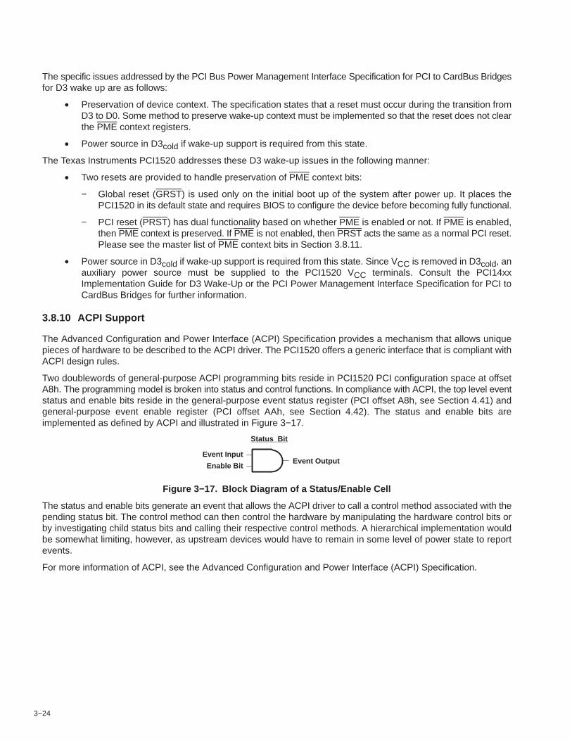
3−24
The specific issues addressed by the PCI Bus Power Management Interface Specification for PCI to CardBus Bridgesfor D3 wake up are as follows:
• Preservation of device context. The specification states that a reset must occur during the transition fromD3 to D0. Some method to preserve wake-up context must be implemented so that the reset does not clearthe PME context registers.
• Power source in D3cold if wake-up support is required from this state.
The Texas Instruments PCI1520 addresses these D3 wake-up issues in the following manner:
• Two resets are provided to handle preservation of PME context bits:
− Global reset (GRST) is used only on the initial boot up of the system after power up. It places thePCI1520 in its default state and requires BIOS to configure the device before becoming fully functional.
− PCI reset (PRST) has dual functionality based on whether PME is enabled or not. If PME is enabled,then PME context is preserved. If PME is not enabled, then PRST acts the same as a normal PCI reset.Please see the master list of PME context bits in Section 3.8.11.
• Power source in D3cold if wake-up support is required from this state. Since VCC is removed in D3cold, anauxiliary power source must be supplied to the PCI1520 VCC terminals. Consult the PCI14xxImplementation Guide for D3 Wake-Up or the PCI Power Management Interface Specification for PCI toCardBus Bridges for further information.
3.8.10 ACPI Support
The Advanced Configuration and Power Interface (ACPI) Specification provides a mechanism that allows uniquepieces of hardware to be described to the ACPI driver. The PCI1520 offers a generic interface that is compliant withACPI design rules.
Two doublewords of general-purpose ACPI programming bits reside in PCI1520 PCI configuration space at offsetA8h. The programming model is broken into status and control functions. In compliance with ACPI, the top level eventstatus and enable bits reside in the general-purpose event status register (PCI offset A8h, see Section 4.41) andgeneral-purpose event enable register (PCI offset AAh, see Section 4.42). The status and enable bits areimplemented as defined by ACPI and illustrated in Figure 3−17.
Event OutputEvent Input
Enable Bit
Status Bit
Figure 3−17. Block Diagram of a Status/Enable Cell
The status and enable bits generate an event that allows the ACPI driver to call a control method associated with thepending status bit. The control method can then control the hardware by manipulating the hardware control bits orby investigating child status bits and calling their respective control methods. A hierarchical implementation wouldbe somewhat limiting, however, as upstream devices would have to remain in some level of power state to reportevents.
For more information of ACPI, see the Advanced Configuration and Power Interface (ACPI) Specification.

3−25
3.8.11 Master List of PME Context Bits and Global Reset-Only Bits
If the PME enable bit (bit 8) of the power-management control/status register (PCI offset A4h, see section 4.38) isasserted, then the assertion of PRST will not clear the following PME context bits. If the PME enable bit is not asserted,then the PME context bits are cleared with PRST. The PME context bits are:
• Bridge control register (PCI offset 3Eh): bit 6• System control register (PCI offset 80h): bits 10, 9, 8• Power-management control/status register (PCI offset A4h): bits 15, 8• ExCA power control register (ExCA offset 802h): bits 7, 5†, 4−3, 1−0 († 82365SL mode only)• ExCA interrupt and general control register (ExCA offset 803h): bits 6−5• ExCA card status change register (ExCA offset 804h): bits 11−8, 3−0• ExCA card status-change-interrupt configuration register (ExCA offset 805h): bits 3−0• CardBus socket event register (CardBus offset 00h): bits 3−0• CardBus socket mask register (CardBus offset 04h): bits 3−0• CardBus socket present state register (CardBus offset 08h): bits 13−7, 5−1• CardBus socket control register (CardBus offset 10h): bits 6−4, 2−0
Global reset places all registers in their default state regardless of the state of the PME enable bit. The GRST signalis gated only by the SUSPEND signal. This means that assertion of SUSPEND blocks the GRST signal internally,thus preserving all register contents. The registers cleared only by GRST are:
• Status register (PCI offset 06h): bits 15−11, 8• Secondary status register (PCI offset 16h): bits 15−11, 8• Interrupt pin register (PCI offset 3Dh): bits 1,0 (function 1 only)• Subsystem vendor ID register (PCI offset 40h): bits 15–0• Subsystem ID register (PCI offset 42h): bits 15–0• PC Card 16-bit legacy mode base address register (PCI offset 44h): bits 31–1• System control register (PCI offset 80h): bits 31–29, 27–13, 11, 6−0• Multifunction routing register (PCI offset 8Ch): bits 27−0• Retry status register (PCI offset 90h): bits 7−5, 3, 1• Card control register (PCI offset 91h): bits 7−5, 2−0• Device control register (PCI offset 92h): bits 7−5, 3−0• Diagnostic register (PCI offset 93h): bits 7−0• Power management capabilities register (PCI offset A2h): bit 15• General-purpose event status register (PCI offset A8h): bits 15−14• General-purpose event enable register (PCI offset AAh): bits 15−14, 11, 8, 4−0• General-purpose output (PCI offset AEh): bits 4−0• Serial bus data (PCI offset B0h): bits 7−0• Serial bus index (PCI offset B1h): bits 7−0• Serial bus slave address register (PCI offset B2h): bits 7−0• Serial bus control and status register (PCI offset B3h): bits 7, 5−0• ExCA identification and revision register (ExCA offset 00h): bits 7−0• ExCA global control register (ExCA offset 1Eh): bits 2−0• Socket present state register (CardBus offset 08h): bit 29• Socket power management register (CardBus offset 20h): bits 25−24

3−26

4−1
4 PC Card Controller Programming Model
This section describes the PCI1520 PCI configuration registers that make up the 256-byte PCI configuration headerfor each PCI1520 function. As noted, some bits are global in nature and are accessed only through function 0.
4.1 PCI Configuration Registers (Functions 0 and 1)
The PCI1520 is a multifunction PCI device, and the PC Card controller is integrated as PCI functions 0 and 1. Theconfiguration header is compliant with the PCI Local Bus Specification as a CardBus bridge header and is PC 99compliant as well. Table 4−1 shows the PCI configuration header, which includes both the predefined portion of theconfiguration space and the user-definable registers.
Table 4−1. PCI Configuration Registers (Functions 0 and 1)REGISTER NAME OFFSET
Device ID Vendor ID 00h
Status Command 04h
Class code Revision ID 08h
BIST Header type Latency timer Cache line size 0Ch
CardBus socket/ExCA base address 10h
Secondary status Reserved Capability pointer 14h
CardBus latency timer Subordinate bus number CardBus bus number PCI bus number 18h
CardBus Memory base register 0 1Ch
CardBus Memory limit register 0 20h
CardBus Memory base register 1 24h
CardBus Memory limit register 1 28h
CardBus I/O base register 0 2Ch
CardBus I/O limit register 0 30h
CardBus I/O base register 1 34h
CardBus I/O limit register 1 38h
Bridge control Interrupt pin Interrupt line 3Ch
Subsystem ID Subsystem vendor ID 40h
PC Card 16-bit I/F legacy-mode base address 44h
Reserved 48h−7Ch
System control 80h
Reserved 84h−88h
Multifunction routing 8Ch
Diagnostic Device control Card control Retry status 90h
Reserved 94h−9Ch
Power-management capabilities Next-item pointer Capability ID A0h
Power-management dataPower-managementcontrol/status bridgesupport extensions
Power-management control/status A4h
General-purpose event enable General-purpose event status A8h
General-purpose output General-purpose input ACh
Serial bus control/status Serial bus slave address Serial bus index Serial bus data B0h
Reserved B4h−FCh

4−2
A bit description table, typically included when a register contains bits of more than one type or purpose, indicatesbit field names, which appear in the signal column; a detailed field description, which appears in the function column;and field access tags, which appear in the type column of the bit description table. Table 4−2 describes the fieldaccess tags.
Table 4−2. Bit Field Access Tag DescriptionsACCESS TAG NAME MEANING
R Read Field may be read by software.
W Write Field may be written by software to any value.
S Set Field may be set by a write of 1. Writes of 0 have no effect.
C Clear Field may be cleared by a write of 1. Writes of 0 have no effect.
U Update Field may be autonomously updated by the PCI1520.
4.2 Vendor ID Register
This 16-bit register contains a value allocated by the PCI Special Interest Group (SIG) and identifies the manufacturerof the PCI device. The vendor ID assigned to TI is 104Ch.
Bit 15 14 13 12 11 10 9 8 7 6 5 4 3 2 1 0
Name Vendor ID
Type R R R R R R R R R R R R R R R R
Default 0 0 0 1 0 0 0 0 0 1 0 0 1 1 0 0
Register: Vendor IDOffset: 00h (functions 0, 1)Type: Read-onlyDefault: 104Ch
4.3 Device ID Register
This 16-bit register contains a value assigned to the PCI1520 by TI. The device identification for the PCI1520 isAC55h.
Bit 15 14 13 12 11 10 9 8 7 6 5 4 3 2 1 0
Name Device ID
Type R R R R R R R R R R R R R R R R
Default 1 0 1 0 1 1 0 0 0 1 0 1 0 1 0 1
Register: Device IDOffset: 02h (functions 0, 1)Type: Read-onlyDefault: AC55h

4−3
4.4 Command Register
The command register provides control over the PCI1520 interface to the PCI bus. All bit functions adhere to thedefinitions in PCI Local Bus Specification. None of the bit functions in this register is shared between the two PCI1520PCI functions. Two command registers exist in the PCI1520, one for each function. Software must manipulate thetwo PCI1520 functions as separate entities when enabling functionality through the command register. TheSERR_EN and PERR_EN enable bits in this register are internally wired-OR between the two functions, and thesecontrol bits appear separately according to their software function. See Table 4−3 for a complete description of theregister contents.
Bit 15 14 13 12 11 10 9 8 7 6 5 4 3 2 1 0
Name Command
Type R R R R R R R RW R RW RW R R RW RW RW
Default 0 0 0 0 0 0 0 0 0 0 0 0 0 0 0 0
Register: CommandOffset: 04hType: Read-only, Read/WriteDefault: 0000h
Table 4−3. Command Register DescriptionBIT SIGNAL TYPE FUNCTION
15−10 RSVD R Reserved. Bits 15−10 return 0s when read.
9 FBB_EN RFast back-to-back enable. The PCI1520 does not generate fast back-to-back transactions; therefore, bit 9returns 0 when read.
8 SERR_EN RW
System error (SERR) enable. Bit 8 controls the enable for the SERR driver on the PCI interface. SERR canbe asserted after detecting an address parity error on the PCI bus. Both bits 8 and 6 must be set for thePCI1520 to report address parity errors.
0 = Disable SERR output driver (default)1 = Enable SERR output driver
7 STEP_EN RAddress/data stepping control. The PCI1520 does not support address/data stepping; therefore, bit 7 ishardwired to 0.
6 PERR_EN RW
Parity error response enable. Bit 6 controls the PCI1520 response to parity errors through PERR. Data parityerrors are indicated by asserting PERR, whereas address parity errors are indicated by asserting SERR.
0 = PCI1520 ignores detected parity error (default)1 = PCI1520 responds to detected parity errors
5 VGA_EN RWVGA palette snoop. Bit 5 controls how PCI devices handle accesses to video graphics array (VGA) paletteregisters.
4 MWI_EN RMemory write-and-invalidate enable. Bit 4 controls whether a PCI initiator device can generate memorywrite-and-Invalidate commands. The PCI1520 controller does not support memory write-and-invalidatecommands, but uses memory write commands instead; therefore, this bit is hardwired to 0.
3 SPECIAL RSpecial cycles. Bit 3 controls whether or not a PCI device ignores PCI special cycles. The PCI1520 doesnot respond to special cycle operations; therefore, this bit is hardwired to 0.
2 MAST_EN RW
Bus master control. Bit 2 controls whether or not the PCI1520 can act as a PCI bus initiator (master). ThePCI1520 can take control of the PCI bus only when this bit is set.
0 = Disables the PCI1520 from generating PCI bus accesses (default)1 = Enables the PCI1520 to generate PCI bus accesses
1 MEM_EN RWMemory space enable. Bit 1 controls whether or not the PCI1520 can claim cycles in PCI memory space.
0 = Disables the PCI1520 from responding to memory space accesses (default)1 = Enables the PCI1520 to respond to memory space accesses
0 IO_EN RWI/O space control. Bit 0 controls whether or not the PCI1520 can claim cycles in PCI I/O space.
0 = Disables the PCI1520 from responding to I/O space accesses (default)1 = Enables the PCI1520 to respond to I/O space accesses

4−4
4.5 Status Register
The status register provides device information to the host system. Bits in this register can be read normally. A bitin the status register is reset when a 1 is written to that bit location; a 0 written to a bit location has no effect. All bitfunctions adhere to the definitions in the PCI Local Bus Specification. PCI bus status is shown through each function.See Table 4−4 for a complete description of the register contents.
Bit 15 14 13 12 11 10 9 8 7 6 5 4 3 2 1 0
Name Status
Type RC RC RC RC RC R R RC R R R R R R R R
Default 0 0 0 0 0 0 1 0 0 0 0 1 0 0 0 0
Register: StatusOffset: 06h (functions 0, 1)Type: Read-only, Read/ClearDefault: 0210h
Table 4−4. Status Register DescriptionBIT SIGNAL TYPE FUNCTION
15 PAR_ERR RC Detected parity error. Bit 15 is set when a parity error is detected (either address or data).
14 SYS_ERR RC Signaled system error. Bit 14 is set when SERR is enabled and the PCI1520 signals a system error to the host.
13 MABORT RCReceived master abort. Bit 13 is set when a cycle initiated by the PCI1520 on the PCI bus is terminated by amaster abort.
12 TABT_REC RCReceived target abort. Bit 12 is set when a cycle initiated by the PCI1520 on the PCI bus is terminated by a targetabort.
11 TABT_SIG RCSignaled target abort. Bit 11 is set by the PCI1520 when it terminates a transaction on the PCI bus with a targetabort.
10−9 PCI_SPEED RDEVSEL timing. These bits encode the timing of DEVSEL and are hardwired 01b, indicating that the PCI1520asserts PCI_SPEED at a medium speed on nonconfiguration cycle accesses.
8 DATAPAR RC
Data parity error detected.0 = The conditions for setting bit 8 have not been met.1 = A data parity error occurred, and the following conditions were met:
a. PERR was asserted by any PCI device including the PCI1520. b. The PCI1520 was the bus master during the data parity error. c. The parity error response bit is set in the command register (PCI offset 04h, see Section 4.4).
7 FBB_CAP RFast back-to-back capable. The PCI1520 cannot accept fast back-to-back transactions; therefore, bit 7 ishardwired to 0.
6 UDF RUser-definable feature support. The PCI1520 does not support the user-definable features; therefore, bit 6 ishardwired to 0.
5 66MHZ R66-MHz capable. The PCI1520 operates at a maximum PCLK frequency of 33 MHz; therefore, bit 5 is hardwiredto 0.
4 CAPLIST RCapabilities list. Bit 4 returns 1 when read. This bit indicates that capabilities in addition to standard PCIcapabilities are implemented. The linked list of PCI power-management capabilities is implemented in thisfunction.
3−0 RSVD R Reserved. Bits 3−0 return 0s when read.

4−5
4.6 Revision ID Register
The revision ID register indicates the silicon revision of the PCI1520.
Bit 7 6 5 4 3 2 1 0
Name Revision ID
Type R R R R R R R R
Default 0 0 0 0 0 0 0 1
Register: Revision IDOffset: 08h (functions 0, 1)Type: Read-onlyDefault: 01h
4.7 PCI Class Code Register
The class code register recognizes PCI1520 functions 0 and 1 as a bridge device (06h) and a CardBus bridge device(07h), with a 00h programming interface.
Bit 23 22 21 20 19 18 17 16 15 14 13 12 11 10 9 8 7 6 5 4 3 2 1 0
Name PCI class code
Base class Subclass Programming interface
Type R R R R R R R R R R R R R R R R R R R R R R R R
Default 0 0 0 0 0 1 1 0 0 0 0 0 0 1 1 1 0 0 0 0 0 0 0 0
Register: PCI class codeOffset: 09h (functions 0, 1)Type: Read-onlyDefault: 06 0700h
4.8 Cache Line Size Register
The cache line size register is programmed by host software to indicate the system cache line size.
Bit 7 6 5 4 3 2 1 0
Name Cache line size
Type RW RW RW RW RW RW RW RW
Default 0 0 0 0 0 0 0 0
Register: Cache line sizeOffset: 0Ch (functions 0, 1)Type: Read/WriteDefault: 00h

4−6
4.9 Latency Timer Register
The latency timer register specifies the latency time for the PCI1520 in units of PCI clock cycles. When the PCI1520is a PCI bus initiator and asserts FRAME, the latency timer begins counting from zero. If the latency timer expiresbefore the PCI1520 transaction has terminated, then the PCI1520 terminates the transaction when its GNT isdeasserted. This register is separate for each of the two PCI1520 functions. This allows platforms to prioritize useof the PCI bus by the two PCI1520 functions.
Bit 7 6 5 4 3 2 1 0
Name Latency timer
Type RW RW RW RW RW RW RW RW
Default 0 0 0 0 0 0 0 0
Register: Latency timerOffset: 0DhType: Read/WriteDefault: 00h
4.10 Header Type Register
This register returns 82h when read, indicating that the PCI1520 function 0 and 1 configuration spaces adhere to theCardBus bridge PCI header. The CardBus bridge PCI header ranges from PCI register 000h to 7Fh, and 80h to FFhis user-definable extension registers.
Bit 7 6 5 4 3 2 1 0
Name Header type
Type R R R R R R R R
Default 1 0 0 0 0 0 1 0
Register: Header typeOffset: 0Eh (functions 0, 1)Type: Read/WriteDefault: 82h
4.11 BIST Register
Because the PCI1520 does not support a built-in self-test (BIST), this register returns the value of 00h when read.
Bit 7 6 5 4 3 2 1 0
Name BIST
Type R R R R R R R R
Default 0 0 0 0 0 0 0 0
Register: BISTOffset: 0Fh (functions 0, 1)Type: Read-onlyDefault: 00h

4−7
4.12 CardBus Socket/ExCA Base-Address Register
The CardBus socket/ExCA base-address register is programmed with a base address referencing the CardBussocket registers and the memory-mapped ExCA register set. Bits 31−12 are read/write and allow the base addressto be located anywhere in the 32-bit PCI memory address space on a 4-Kbyte boundary. Bits 11−0 are read-only,returning 0s when read. When software writes all 1s to this register, the value read back is FFFF F000h, indicatingthat at least 4 Kbytes of memory address space are required. The CardBus registers start at offset 000h, and thememory-mapped ExCA registers begin at offset 800h. Because this register is not shared by functions 0 and 1,mapping of each socket control is performed separately.
Bit 31 30 29 28 27 26 25 24 23 22 21 20 19 18 17 16
Name CardBus socket/ExCA base-address
Type RW RW RW RW RW RW RW RW RW RW RW RW RW RW RW RW
Default 0 0 0 0 0 0 0 0 0 0 0 0 0 0 0 0
Bit 15 14 13 12 11 10 9 8 7 6 5 4 3 2 1 0
Name CardBus socket/ExCA base-address
Type RW RW RW RW R R R R R R R R R R R R
Default 0 0 0 0 0 0 0 0 0 0 0 0 0 0 0 0
Register: CardBus socket/ExCA base-addressOffset: 10hType: Read-only, Read/WriteDefault: 0000 0000h
4.13 Capability Pointer Register
The capability pointer register provides a pointer into the PCI configuration header where the PCIpower-management register block resides. PCI header doublewords at A0h and A4h provide the power-management(PM) registers. Each socket has its own capability pointer register. This register returns A0h when read.
Bit 7 6 5 4 3 2 1 0
Name Capability pointer
Type R R R R R R R R
Default 1 0 1 0 0 0 0 0
Register: Capability pointerOffset: 14hType: Read-onlyDefault: A0h

4−8
4.14 Secondary Status Register
The secondary status register is compatible with the PCI-to-PCI bridge secondary status register and indicatesCardBus-related device information to the host system. This register is very similar to the status register (offset 06h,see Section 4.5); status bits are cleared by writing a 1. See Table 4−5 for a complete description of the registercontents.
Bit 15 14 13 12 11 10 9 8 7 6 5 4 3 2 1 0
Name Secondary status
Type RC RC RC RC RC R R RC R R R R R R R R
Default 0 0 0 0 0 0 1 0 0 0 0 0 0 0 0 0
Register: Secondary statusOffset: 16hType: Read-only, Read/ClearDefault: 0200h
Table 4−5. Secondary Status Register DescriptionBIT SIGNAL TYPE FUNCTION
15 CBPARITY RC Detected parity error. Bit 15 is set when a CardBus parity error is detected (either address or data).
14 CBSERR RCSignaled system error. Bit 14 is set when CSERR is signaled by a CardBus card. The PCI1520 does notassert CSERR.
13 CBMABORT RCReceived master abort. Bit 13 is set when a cycle initiated by the PCI1520 on the CardBus bus has beenterminated by a master abort.
12 REC_CBTA RCReceived target abort. Bit 12 is set when a cycle initiated by the PCI1520 on the CardBus bus is terminatedby a target abort.
11 SIG_CBTA RCSignaled target abort. Bit 11 is set by the PCI1520 when it terminates a transaction on the CardBus buswith a target abort.
10−9 CB_SPEED RCDEVSEL timing. These bits encode the timing of CDEVSEL and are hardwired 01b, indicating that thePCI1520 asserts CB_SPEED at a medium speed.
8 CB_DPAR RC
CardBus data parity error detected.0 = The conditions for setting bit 8 have not been met.1 = A data parity error occurred and the following conditions were met:
a. CPERR was asserted on the CardBus interface. b. The PCI1520 was the bus master during the data parity error. c. The parity error response bit is set in the bridge control.
7 CBFBB_CAP RFast back-to-back capable. The PCI1520 cannot accept fast back-to-back transactions; therefore, bit 7is hardwired to 0.
6 CB_UDF RUser-definable feature support. The PCI1520 does not support user-definable features; therefore, bit 6is hardwired to 0.
5 CB66MHZ R66-MHz capable. The PCI1520 CardBus interface operates at a maximum CCLK frequency of 33 MHz;therefore, bit 5 is hardwired to 0.
4−0 RSVD R Reserved. Bits 4−0 return 0s when read.

4−9
4.15 PCI Bus Number Register
This register is programmed by the host system to indicate the bus number of the PCI bus to which the PCI1520 isconnected. The PCI1520 uses this register in conjunction with the CardBus bus number and subordinate bus numberregisters to determine when to forward PCI configuration cycles to its secondary buses.
Bit 7 6 5 4 3 2 1 0
Name PCI bus number
Type RW RW RW RW RW RW RW RW
Default 0 0 0 0 0 0 0 0
Register: PCI bus numberOffset: 18h (functions 0, 1)Type: Read/WriteDefault: 00h
4.16 CardBus Bus Number Register
This register is programmed by the host system to indicate the bus number of the CardBus bus to which the PCI1520is connected. The PCI1520 uses this register in conjunction with the PCI bus number and subordinate bus numberregisters to determine when to forward PCI configuration cycles to its secondary buses. This register is separate foreach PCI1520 controller function.
Bit 7 6 5 4 3 2 1 0
Name CardBus bus number
Type RW RW RW RW RW RW RW RW
Default 0 0 0 0 0 0 0 0
Register: CardBus bus numberOffset: 19hType: Read/WriteDefault: 00h
4.17 Subordinate Bus Number Register
This register is programmed by the host system to indicate the highest-numbered bus below the CardBus bus. ThePCI1520 uses this register in conjunction with the PCI bus number and CardBus bus number registers to determinewhen to forward PCI configuration cycles to its secondary buses. This register is separate for each CardBus controllerfunction.
Bit 7 6 5 4 3 2 1 0
Name Subordinate bus number
Type RW RW RW RW RW RW RW RW
Default 0 0 0 0 0 0 0 0
Register: Subordinate bus numberOffset: 1AhType: Read/WriteDefault: 00h

4−10
4.18 CardBus Latency Timer Register
This register is programmed by the host system to specify the latency timer for the PCI1520 CardBus interface in unitsof CCLK cycles. When the PCI1520 is a CardBus initiator and asserts CFRAME, the CardBus latency timer beginscounting. If the latency timer expires before the PCI1520 transaction has terminated, then the PCI1520 terminatesthe transaction at the end of the next data phase. A recommended minimum value for this register is 40h, which allowsmost transactions to be completed.
Bit 7 6 5 4 3 2 1 0
Name CardBus latency timer
Type RW RW RW RW RW RW RW RW
Default 0 0 0 0 0 0 0 0
Register: CardBus latency timerOffset: 1Bh (functions 0, 1)Type: Read/WriteDefault: 00h
4.19 Memory Base Registers 0, 1
The memory base registers indicate the lower address of a PCI memory address range. These registers are usedby the PCI1520 to determine when to forward a memory transaction to the CardBus bus and when to forward aCardBus cycle to PCI. Bits 31−12 of these registers are read/write and allow the memory base to be located anywherein the 32-bit PCI memory space on 4-Kbyte boundaries. Bits 11−0 are read-only and always return 0s. Writetransactions to these bits have no effect. Bits 8 and 9 of the bridge control register specify whether memory windows0 and 1 are prefetchable or nonprefetchable. The memory base register or the memory limit register must be nonzerofor the PCI1520 to claim any memory transactions through CardBus memory windows (that is, these windows arenot enabled by default to pass the first 4 Kbytes of memory to CardBus).
Bit 31 30 29 28 27 26 25 24 23 22 21 20 19 18 17 16
Name Memory base registers 0, 1
Type RW RW RW RW RW RW RW RW RW RW RW RW RW RW RW RW
Default 0 0 0 0 0 0 0 0 0 0 0 0 0 0 0 0
Bit 15 14 13 12 11 10 9 8 7 6 5 4 3 2 1 0
Name Memory base registers 0, 1
Type RW RW RW RW R R R R R R R R R R R R
Default 0 0 0 0 0 0 0 0 0 0 0 0 0 0 0 0
Register: Memory base registers 0, 1Offset: 1Ch, 24hType: Read-only, Read/WriteDefault: 0000 0000h

4−11
4.20 Memory Limit Registers 0, 1
The memory limit registers indicate the upper address of a PCI memory address range. These registers are usedby the PCI1520 to determine when to forward a memory transaction to the CardBus bus and when to forward aCardBus cycle to PCI. Bits 31−12 of these registers are read/write and allow the memory base to be located anywherein the 32-bit PCI memory space on 4-Kbyte boundaries. Bits 11−0 are read-only and always return 0s. Writetransactions to these bits have no effect. Bits 8 and 9 of the bridge control register specify whether memory windows0 and 1 are prefetchable or nonprefetchable. The memory base register or the memory limit register must be nonzerofor the PCI1520 to claim any memory transactions through CardBus memory windows; that is, these windows arenot enabled by default to pass the first 4 Kbytes of memory to CardBus.
Bit 31 30 29 28 27 26 25 24 23 22 21 20 19 18 17 16
Name Memory limit registers 0, 1
Type RW RW RW RW RW RW RW RW RW RW RW RW RW RW RW RW
Default 0 0 0 0 0 0 0 0 0 0 0 0 0 0 0 0
Bit 15 14 13 12 11 10 9 8 7 6 5 4 3 2 1 0
Name Memory limit registers 0, 1
Type RW RW RW RW R R R R R R R R R R R R
Default 0 0 0 0 0 0 0 0 0 0 0 0 0 0 0 0
Register: Memory limit registers 0, 1Offset: 20h, 28hType: Read-only, Read/WriteDefault: 0000 0000h
4.21 I/O Base Registers 0, 1
The I/O base registers indicate the lower address of a PCI I/O address range. These registers are used by thePCI1520 to determine when to forward an I/O transaction to the CardBus bus and when to forward a CardBus cycleto the PCI bus. The lower 16 bits of this register locate the bottom of the I/O window within a 64-Kbyte page, and theupper 16 bits (31−16) are a page register which locates this 64-Kbyte page in 32-bit PCI I/O address space. Bits 31−2are read/write. Bits 1 and 0 are read-only and always return 0s, forcing I/O windows to be aligned on a naturaldoubleword boundary.
NOTE: Either the I/O base register or the I/O limit register must be nonzero to enable any I/Otransactions.
Bit 31 30 29 28 27 26 25 24 23 22 21 20 19 18 17 16
Name I/O base registers 0, 1
Type RW RW RW RW RW RW RW RW RW RW RW RW RW RW RW RW
Default 0 0 0 0 0 0 0 0 0 0 0 0 0 0 0 0
Bit 15 14 13 12 11 10 9 8 7 6 5 4 3 2 1 0
Name I/O base registers 0, 1
Type RW RW RW RW RW RW RW RW RW RW RW RW RW RW R R
Default 0 0 0 0 0 0 0 0 0 0 0 0 0 0 0 0
Register: I/O base registers 0, 1Offset: 2Ch, 34hType: Read-only, Read/WriteDefault: 0000 0000h

4−12
4.22 I/O Limit Registers 0, 1
The I/O limit registers indicate the upper address of a PCI I/O address range. These registers are used by the PCI1520to determine when to forward an I/O transaction to the CardBus bus and when to forward a CardBus cycle to PCI.The lower 16 bits of this register locate the top of the I/O window within a 64-Kbyte page, and the upper 16 bits area page register that locates this 64-Kbyte page in 32-bit PCI I/O address space. Bits 15−2 are read/write and allowthe I/O limit address to be located anywhere in the 64-Kbyte page (indicated by bits 31−16 of the appropriate I/O base)on doubleword boundaries.
Bits 31−16 are read-only and always return 0s when read. The page is set in the I/O base register. Bits 1 and 0 areread-only and always return 0s, forcing I/O windows to be aligned on a natural doubleword boundary. Writetransactions to read-only bits have no effect. The PCI1520 assumes that the lower 2 bits of the limit address are 1s.
NOTE: The I/O base or the I/O limit register must be nonzero to enable an I/O transaction.
Bit 31 30 29 28 27 26 25 24 23 22 21 20 19 18 17 16
Name I/O limit registers 0, 1
Type R R R R R R R R R R R R R R R R
Default 0 0 0 0 0 0 0 0 0 0 0 0 0 0 0 0
Bit 15 14 13 12 11 10 9 8 7 6 5 4 3 2 1 0
Name I/O limit registers 0, 1
Type RW RW RW RW RW RW RW RW RW RW RW RW RW RW R R
Default 0 0 0 0 0 0 0 0 0 0 0 0 0 0 0 0
Register: I/O limit registers 0, 1Offset: 30h, 38hType: Read-only, Read/WriteDefault: 0000 0000h
4.23 Interrupt Line Register
The interrupt line register communicates interrupt line routing information. Each PCI1520 function has an interruptline register.
Bit 7 6 5 4 3 2 1 0
Name Interrupt line
Type RW RW RW RW RW RW RW RW
Default 1 1 1 1 1 1 1 1
Register: Interrupt lineOffset: 3ChType: Read/WriteDefault: FFh

4−13
4.24 Interrupt Pin Register
The value read from the interrupt pin register is function dependent and depends on the interrupt signaling mode,selected through bits 2−1 (INTMODE field) of the device control register (PCI offset 92h, see Section 4.33) and thestate of bit 29 (INTRTIE) in the system control register (PCI offset 80h, see Section 4.29). When the INTRTIE bit isset, this register reads 01h (INTA) for both functions. See Table 4−6 for a complete description of the register contents.
Bit 7 6 5 4 3 2 1 0
Name Interrupt pin
Type R R R R R R R R
Default 0 0 0 0 0 0 X X
Register: Interrupt pinOffset: 3DhType: Read-onlyDefault: 0Xh
Table 4−6. Interrupt Pin Register Cross-Reference
INTRTIE BITINTPIN
INTRTIE BITFUNCTION 0 FUNCTION 1
0 01h 02h
1 01h 01h
4−14
4.25 Bridge Control Register
The bridge control register provides control over various PCI1520 bridging functions. Some bits in this register areglobal and are accessed only through function 0. See Table 4−7 for a complete description of the register contents.
Bit 15 14 13 12 11 10 9 8 7 6 5 4 3 2 1 0
Name Bridge control
Type R R R R R RW RW RW RW RW RW R RW RW RW RW
Default 0 0 0 0 0 0 1 1 0 1 0 0 0 0 0 0
Register: Bridge controlOffset: 3Eh (functions 0, 1)Type: Read-only, Read/WriteDefault: 0340h
Table 4−7. Bridge Control Register DescriptionBIT SIGNAL TYPE FUNCTION
15−11 RSVD R Reserved. Bits 15−11 return 0s when read.
10 POSTEN RW
Write posting enable. Enables write posting to and from the CardBus sockets. Write posting enablesposting of write data on burst cycles. Operating with write posting disabled inhibits performance on burstcycles. Note that burst write data can be posted, but various write transactions may not. Bit 10 is socketdependent and is not shared between functions 0 and 1.
9 PREFETCH1 RW
Memory window 1 type. Bit 9 specifies whether or not memory window 1 is prefetchable. This bit is socketdependent. Bit 9 is encoded as:
0 = Memory window 1 is nonprefetchable.1 = Memory window 1 is prefetchable (default).
8 PREFETCH0 RW
Memory window 0 type. Bit 8 specifies whether or not memory window 0 is prefetchable. This bit isencoded as:
0 = Memory window 0 is nonprefetchable.1 = Memory window 0 is prefetchable (default).
7 INTR RW
PCI interrupt − IREQ routing enable. Bit 7 selects whether PC Card functional interrupts are routed to PCIinterrupts or the IRQ specified in the ExCA registers.
0 = Functional interrupts routed to PCI interrupts (default)1 = Functional interrupts routed by ExCAs
6 CRST RW
CardBus reset. When bit 6 is set, CRST is asserted on the CardBus interface. CRST can also be assertedby passing a PRST assertion to CardBus.
0 = CRST deasserted1 = CRST asserted (default)
5† MABTMODE RW
Master abort mode. Bit 5 controls how the PCI1520 responds to a master abort when the PCI1520 is aninitiator on the CardBus interface. This bit is common between each socket.
0 = Master aborts not reported (default)1 = Signal target abort on PCI and SERR (if enabled)
4 RSVD R Reserved. Bit 4 returns 0 when read.
3 VGAEN RWVGA enable. Bit 3 affects how the PCI1520 responds to VGA addresses. When this bit is set, accessesto VGA addresses are forwarded.
2 ISAEN RWISA mode enable. Bit 2 affects how the PCI1520 passes I/O cycles within the 64-Kbyte ISA range. Thisbit is not common between sockets. When this bit is set, the PCI1520 does not forward the last 768 bytesof each 1K I/O range to CardBus.
1† CSERREN RW
CSERR enable. Bit 1 controls the response of the PCI1520 to CSERR signals on the CardBus bus. Thisbit is common between the two sockets.
0 = CSERR is not forwarded to PCI SERR.1 = CSERR is forwarded to PCI SERR.
0† CPERREN RW
CardBus parity error response enable. Bit 0 controls the response of the PCI1520 to CardBus parity errors.This bit is common between the two sockets.
0 = CardBus parity errors are ignored.1 = CardBus parity errors are reported using CPERR.
† This bit is global and is accessed only through function 0.

4−15
4.26 Subsystem Vendor ID Register
The subsystem vendor ID register is used for system and option-card identification purposes and may be requiredfor certain operating systems. This register is read-only or read/write, depending on the setting of bit 5 (SUBSYSRW)in the system control register (PCI offset 80h, see Section 4.29).
Bit 15 14 13 12 11 10 9 8 7 6 5 4 3 2 1 0
Name Subsystem vendor ID
Type R R R R R R R R R R R R R R R R
Default 0 0 0 0 0 0 0 0 0 0 0 0 0 0 0 0
Register: Subsystem vendor IDOffset: 40h (functions 0, 1)Type: Read-only (Read/Write if enabled by SUBSYSRW)Default: 0000h
4.27 Subsystem ID Register
The subsystem ID register is used for system and option-card identification purposes and may be required for certainoperating systems. This register is read-only or read/write, depending on the setting of bit 5 (SUBSYSRW) in thesystem control register (PCI offset 80h, see Section 4.29).
Bit 15 14 13 12 11 10 9 8 7 6 5 4 3 2 1 0
Name Subsystem ID
Type R R R R R R R R R R R R R R R R
Default 0 0 0 0 0 0 0 0 0 0 0 0 0 0 0 0
Register: Subsystem IDOffset: 42h (functions 0, 1)Type: Read-only (Read/Write if enabled by SUBSYSRW)Default: 0000h
4.28 PC Card 16-Bit I/F Legacy-Mode Base Address Register
The PCI1520 supports the index/data scheme of accessing the ExCA registers, which are mapped by this register.An address written to this register is the address for the index register and the address + 1 is the data address. Usingthis access method, applications requiring index/data ExCA access can be supported. The base address can bemapped anywhere in 32-bit I/O space on a word boundary; hence, bit 0 is read-only, returning 1 when read. Asspecified in the PCI to PCMCIA CardBus Bridge Register Description (Yenta), this register is shared by functions 0and 1. See Section 5, ExCA Compatibility Registers, for register offsets.
Bit 31 30 29 28 27 26 25 24 23 22 21 20 19 18 17 16
Name PC Card 16-bit I/F legacy-mode base address
Type RW RW RW RW RW RW RW RW RW RW RW RW RW RW RW RW
Default 0 0 0 0 0 0 0 0 0 0 0 0 0 0 0 0
Bit 15 14 13 12 11 10 9 8 7 6 5 4 3 2 1 0
Name PC Card 16-bit I/F legacy-mode base address
Type RW RW RW RW RW RW RW RW RW RW RW RW RW RW RW R
Default 0 0 0 0 0 0 0 0 0 0 0 0 0 0 0 1
Register: PC Card 16-bit I/F legacy-mode base addressOffset: 44h (functions 0, 1)Type: Read-only, Read/WriteDefault: 0000 0001h

4−16
4.29 System Control Register
System-level initializations are performed by programming this doubleword register. Some of the bits are global andare written only through function 0. See Table 4−8 for a complete description of the register contents.
Bit 31 30 29 28 27 26 25 24 23 22 21 20 19 18 17 16
Name System control
Type RW RW RW R RW RW RC RW R RW RW RW RW RW RW RW
Default 0 0 0 0 0 0 0 0 0 1 0 0 0 1 0 0
Bit 15 14 13 12 11 10 9 8 7 6 5 4 3 2 1 0
Name System control
Type RW RW R R R R R R R RW RW RW RW RW RW RW
Default 1 0 0 1 0 0 0 0 0 1 1 0 0 0 0 0
Register: System controlOffset: 80h (functions 0, 1)Type: Read-only, Read/Write, Read/ClearDefault: 0044 9060h

4−17
Table 4−8. System Control Register DescriptionBIT SIGNAL TYPE FUNCTION
31−30† SER_STEP RW
Serialized PCI interrupt routing step. Bits 31 and 30 configure the serialized PCI interrupt stream signalingand accomplish an even distribution of interrupts signaled on the four PCI interrupt slots. Bits 31 and 30 areglobal to all PCI1520 functions.
00 = INTA/INTB signal in INTA/INTB IRQSER slots01 = INTA/INTB signal in INTB/INTC IRQSER slots10 = INTA/INTB signal in INTC/INTD IRQSER slots11 = INTA/INTB signal in INTD/INTA IRQSER slots
29† INTRTIE RW
Tie internal PCI interrupts. When this bit is set, the INTA and INTB signals are tied together internally and aresignaled as INTA. INTA can then be shifted by using bits 31−30 (SER_STEP). This bit is global to all PCI1520functions.When configuring the PCI1520 functions to share PCI interrupts, multifunction terminal MFUNC3 must beconfigured as IRQSER prior to setting the INTRTIE bit.
28 RSVD R Reserved. Bit 28 returns 0 when read.
27† P2CCLK RW
P2C power switch clock. The PCI1520 CLOCK signal is used to clock the serial interface power switch andthe internal state machine. The default state for bit 27 is 0, requiring an external clock source provided to theCLOCK terminal (terminal number F15 for the GHK package or terminal number 154 for the PDV package).Bit 27 can be set to 1, allowing the internal oscillator to provide the clock signal.
0 = CLOCK provided externally, input to PCI1520 (default)1 = CLOCK generated by internal oscillator and driven by PCI1520.
26 SMIROUTE RW
SMI interrupt routing. Bit 26 is shared between functions 0 and 1, and selects whether IRQ2 or CSC is signaledwhen a write occurs to power a PC Card socket.
0 = PC Card power change interrupts routed to IRQ2 (default)1 = A CSC interrupt is generated on PC Card power changes.
25 SMISTATUS RC
SMI interrupt status. This socket-dependent bit is set when bit 24 (SMIENB) is set and a write occurs to setthe socket power. Writing a 1 to bit 25 clears the status.
0 = SMI interrupt signaled (default)1 = SMI interrupt not signaled
24† SMIENB RWSMI interrupt mode enable. When bit 24 is set and a write to the socket power control occurs, the SMI interruptsignaling is enabled and generates an interrupt. This bit is shared and defaults to 0 (disabled).
23 RSVD R Reserved. Bit 23 returns 0 when read.
22 CBRSVD RW
CardBus reserved terminals signaling. When a CardBus card is inserted and bit 22 is set, the RSVD CardBusterminals are driven low. When this bit is 0, these terminals are placed in a high-impedance state.
0 = Place CardBus RSVD terminals in a high-impedance state.1 = Drive Cardbus RSVD terminals low (default).
21 VCCPROT RWVCC protection enable. Bit 21 is socket dependent.
0 = VCC protection enabled for 16-bit cards (default)1 = VCC protection disabled for 16-bit cards
20 REDUCEZV RW
Reduced zoomed video enable. When this bit is enabled, terminals A25−A22 of the card interface for PCCard-16 cards are placed in the high-impedance state. This bit should not be set for normal ZV operation. Thisbit is encoded as:
0 = Reduced zoomed video disabled (default)1 = Reduced zoomed video enabled
19−16 RSVD RW Reserved. Do not change the default value.
15† MRBURSTDN
RW
Memory read burst enable downstream. When bit 15 is set, memory read transactions are allowed to burstdownstream.
0 = Downstream memory read burst is disabled.1 = Downstream memory read burst is enabled (default).
14† MRBURSTUP
RW
Memory read burst enable upstream. When bit 14 is set, the PCI1520 allows memory read transactions toburst upstream.
0 = Upstream memory read burst is disabled (default).1 = Upstream memory read burst is enabled.
13SOCACTIV
ER
Socket activity status. When set, bit 13 indicates access has been performed to or from a PC card and iscleared upon read of this status bit. This bit is socket-dependent.
0 = No socket activity (default)1 = Socket activity
12 RSVD R Reserved. Bit 12 returns 1 when read.
† This bit is global and is accessed only through function 0.

4−18
Table 4−8. System Control Register Description (Continued)BIT SIGNAL TYPE FUNCTION
11† PWRSTREAM R
Power stream in progress status bit. When set, bit 11 indicates that a power stream to the power switchis in progress and a powering change has been requested. This bit is cleared when the power stream iscomplete.
0 = Power stream is complete and delay has expired.1 = Power stream is in progress.
10† DELAYUP RPower-up delay in progress status. When set, bit 10 indicates that a power-up stream has been sent tothe power switch and proper power may not yet be stable. This bit is cleared when the power-up delay hasexpired.
9† DELAYDOWN RPower-down delay in progress status. When set, bit 9 indicates that a power-down stream has been sentto the power switch and proper power may not yet be stable. This bit is cleared when the power-down delayhas expired.
8 INTERROGATE R
Interrogation in progress. When set, bit 8 indicates an interrogation is in progress and clears wheninterrogation completes. This bit is socket dependent.
0 = Interrogation not in progress (default)1 = Interrogation in progress
7 RSVD R Reserved. Bit 7 returns 0 when read.
6 PWRSAVINGS RWPower savings mode enable. When this bit is set, if a CB card is inserted, idle, and without a CB clock,then the applicable CB state machine will not be clocked.
5† SUBSYSRW RW
Subsystem ID (PCI offset 42h, see Section 4.27), subsystem vendor ID (PCI offset 40H, seeSection 4.26), ExCA identification and revision (ExCA offset 00h/40h/800h, see Section 5.1) registersread/write enable. Bit 5 is shared by functions 0 and 1.
0 = Subsystem ID, subsystem vendor ID, ExCA identification and revision registers are read/write.1 = Subsystem ID, subsystem vendor ID, ExCA identification and revision registers are read-only
(default).
4† CB_DPAR RWCardBus data parity SERR signaling enable
0 = CardBus data parity not signaled on PCI SERR1 = CardBus data parity signaled on PCI SERR
3 RSVD RW Reserved. Do not change the default value.
2 EXCAPOWER RWExCA power-control bit.
0 = Enables 3.3 V1 = Enables 5 V
1† KEEPCLK RWKeep clock. This bit works with PCI and CB CLKRUN protocols.
0 = Allows normal functioning of both CLKRUN protocols (default)1 = Does not allow CB clock or PCI clock to be stopped using the CLKRUN protocols
0 RIMUX RW
RI_OUT/PME multiplex enable.0 = RI_OUT and PME are both routed to the RI_OUT/PME terminal. If both functions are are enabled
at the same time, the terminal becomes RI_OUT only and PME assertions are not seen.1 = Only PME is routed to the RI_OUT/PME terminal.
† This bit is global and is accessed only through function 0.

4−19
4.30 Multifunction Routing Register
The multifunction routing register is used to configure the MFUNC0−MFUNC6 terminals. These terminals may beconfigured for various functions. All multifunction terminals default to the general-purpose input configuration. Thisregister is intended to be programmed once at power-on initialization. The default value for this register can also beloaded through a serial bus EEPROM. See Table 4−9 for a complete description of the register contents.Bit 31 30 29 28 27 26 25 24 23 22 21 20 19 18 17 16
Name Multifunction routing
Type R R R R RW RW RW RW RW RW RW RW RW RW RW RW
Default 0 0 0 0 0 0 0 0 0 0 0 0 0 0 0 0
Bit 15 14 13 12 11 10 9 8 7 6 5 4 3 2 1 0
Name Multifunction routing
Type RW RW RW RW RW RW RW RW RW RW RW RW RW RW RW RW
Default 0 0 0 1 0 0 0 0 0 0 0 0 0 0 0 0
Register: Multifunction routingOffset: 8Ch (functions 0, 1)Type: Read-only, Read/WriteDefault: 0000 1000h
Table 4−9. Multifunction Routing Register DescriptionBIT SIGNAL TYPE FUNCTION
31−28 RSVD R Bits 31−28 return 0s when read.
27−24 MFUNC6 RW
Multifunction terminal 6 configuration. These bits control the internal signal mapped to the MFUNC6 terminalas follows:
0000 = RSVD† 0100 = IRQ4 1000 = IRQ8 1100 = IRQ120001 = CLKRUN 0101 = IRQ5 1001 = IRQ9 1101 = IRQ130010 = IRQ2 0110 = IRQ6 1010 = IRQ10 1110 = IRQ140011 = IRQ3 0111 = IRQ7 1011 = IRQ11 1111 = IRQ15
23−20 MFUNC5 RW
Multifunction terminal 5 configuration. These bits control the internal signal mapped to the MFUNC5 terminalas follows:
0000 = GPI4† 0100 = IRQ4 1000 = CAUDPWM 1100 = LEDA10001 = GPO4 0101 = IRQ5 1001 = D3_STAT 1101 = LED_SKT0010 = PCGNT 0110 = ZVSTAT 1010 = IRQ10 1110 = GPE0011 = IRQ3 0111 = ZVSEL1 1011 = IRQ11 1111 = IRQ15
19−16 MFUNC4 RW
Multifunction terminal 4 configuration. These bits control the internal signal mapped to the MFUNC4 terminalas follows:
NOTE: When the serial bus mode is implemented by pulling down the LATCH terminal, the MFUNC4 terminalprovides the SCL signaling.
0000 = GPI3† 0100 = IRQ4 1000 = CAUDPWM 1100 = RI_OUT0001 = GPO3 0101 = IRQ5 1001 = IRQ9 1101 = LED_SKT0010 = LOCK PCI 0110 = ZVSTAT 1010 = IRQ10 1110 = GPE0011 = IRQ3 0111 = ZVSEL1 1011 = IRQ11 1111 = D3_STAT
15−12 MFUNC3 RW
Multifunction terminal 3 configuration. These bits control the internal signal mapped to the MFUNC3 terminalas follows:
0000 = RSVD 0100 = IRQ4 1000 = IRQ8 1100 = IRQ120001 = IRQSER† 0101 = IRQ5 1001 = IRQ9 1101 = IRQ130010 = IRQ2 0110 = IRQ6 1010 = IRQ10 1110 = IRQ140011 = IRQ3 0111 = IRQ7 1011 = IRQ11 1111 = IRQ15
11−8 MFUNC2 RW
Multifunction terminal 2 configuration. These bits control the internal signal mapped to the MFUNC2 terminalas follows:
0000 = GPI2† 0100 = IRQ4 1000 = CAUDPWM 1100 = RI_OUT0001 = GPO2 0101 = IRQ5 1001 = IRQ9 1101 = LEDA20010 = PCREQ 0110 = ZVSTAT 1010 = IRQ10 1110 = GPE0011 = IRQ3 0111 = ZVSEL0 1011 = D3_STAT 1111 = IRQ7
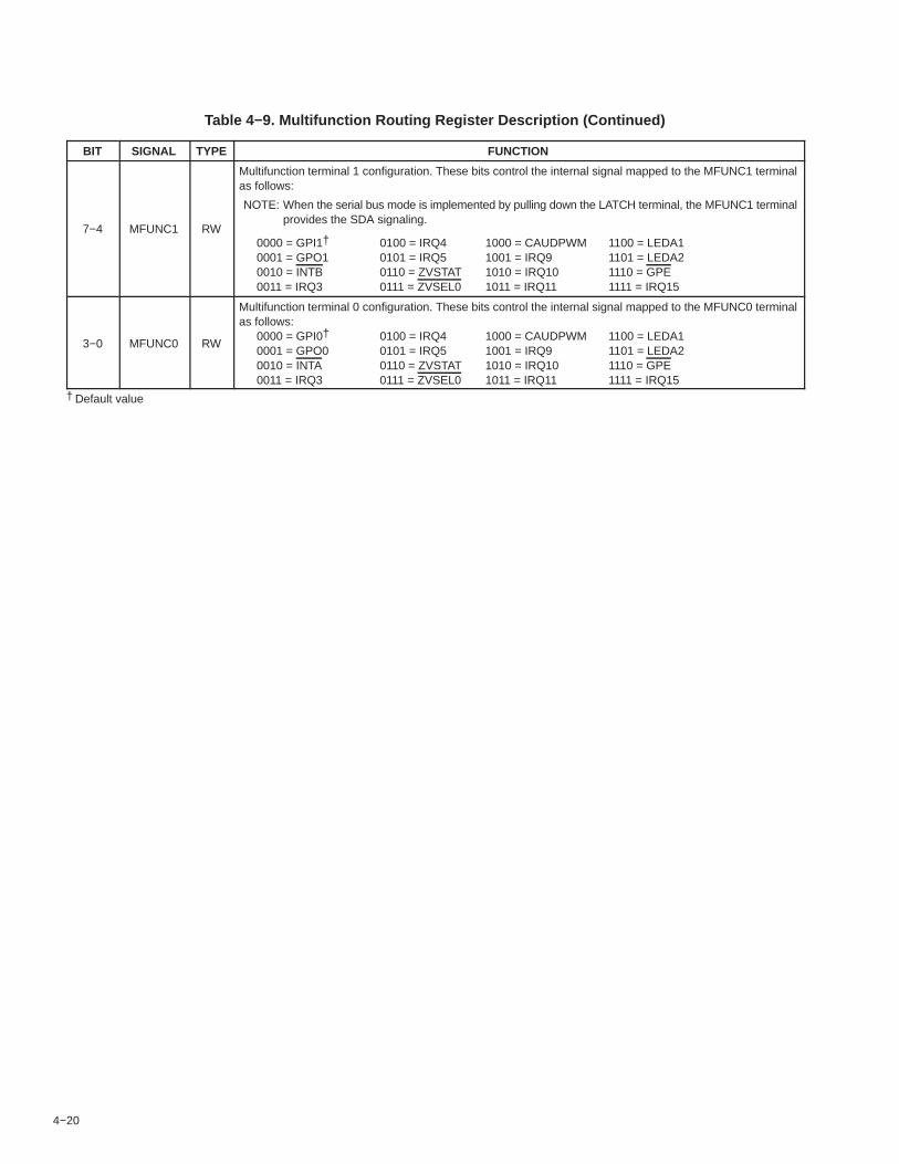
4−20
Table 4−9. Multifunction Routing Register Description (Continued)
BIT SIGNAL TYPE FUNCTION
7−4 MFUNC1 RW
Multifunction terminal 1 configuration. These bits control the internal signal mapped to the MFUNC1 terminalas follows:
NOTE: When the serial bus mode is implemented by pulling down the LATCH terminal, the MFUNC1 terminalprovides the SDA signaling.
0000 = GPI1† 0100 = IRQ4 1000 = CAUDPWM 1100 = LEDA10001 = GPO1 0101 = IRQ5 1001 = IRQ9 1101 = LEDA20010 = INTB 0110 = ZVSTAT 1010 = IRQ10 1110 = GPE0011 = IRQ3 0111 = ZVSEL0 1011 = IRQ11 1111 = IRQ15
3−0 MFUNC0 RW
Multifunction terminal 0 configuration. These bits control the internal signal mapped to the MFUNC0 terminalas follows:
0000 = GPI0† 0100 = IRQ4 1000 = CAUDPWM 1100 = LEDA10001 = GPO0 0101 = IRQ5 1001 = IRQ9 1101 = LEDA20010 = INTA 0110 = ZVSTAT 1010 = IRQ10 1110 = GPE0011 = IRQ3 0111 = ZVSEL0 1011 = IRQ11 1111 = IRQ15
† Default value

4−21
4.31 Retry Status Register
The retry status register enables the retry timeout counters and displays the retry expiration status. The flags are setwhen the PCI1520 retries a PCI or CardBus master request and the master does not return within 215 PCI clockcycles. The flags are cleared by writing a 1 to the bit. These bits are expected to be incorporated into the PCIcommand, PCI status, and bridge control registers by the PCI SIG. Access this register only through function 0. SeeTable 4−10 for a complete description of the register contents.
Bit 7 6 5 4 3 2 1 0
Name Retry status
Type RW RW RC R RC R RC R
Default 1 1 0 0 0 0 0 0
Register: Retry statusOffset: 90h (functions 0, 1)Type: Read-only, Read/Write, Read/ClearDefault: C0h
Table 4−10. Retry Status Register DescriptionBIT SIGNAL TYPE FUNCTION
7 PCIRETRY RWPCI retry timeout counter enable. Bit 7 is encoded:
0 = PCI retry counter disabled1 = PCI retry counter enabled (default)
6† CBRETRY RWCardBus retry timeout counter enable. Bit 6 is encoded:
0 = CardBus retry counter disabled1 = CardBus retry counter enabled (default)
5 TEXP_CBB RCCardBus target B retry expired. Write a 1 to clear bit 5.
0 = Inactive (default)1 = Retry has expired
4 RSVD R Reserved. Bit 4 returns 0 when read.
3† TEXP_CBA RCCardBus target A retry expired. Write a 1 to clear bit 3.
0 = Inactive (default)1 = Retry has expired.
2 RSVD R Reserved. Bit 2 returns 0 when read.
1 TEXP_PCI RCPCI target retry expired. Write a 1 to clear bit 1.
0 = Inactive (default)1 = Retry has expired.
0 RSVD R Reserved. Bit 0 returns 0 when read.† This bit is global and is accessed only through function 0.

4−22
4.32 Card Control Register
The card control register is provided for PCI1130 compatibility. RI_OUT is enabled through this register, and theenable bit is shared between functions 0 and 1. See Table 4−11 for a complete description of the register contents.
Bit 7 6 5 4 3 2 1 0
Name Card control
Type RW RW RW R R RW RW RC
Default 0 0 0 0 0 0 0 0
Register: Card controlOffset: 91hType: Read-only, Read/Write, Read/ClearDefault: 00h
Table 4−11. Card Control Register DescriptionBIT SIGNAL TYPE FUNCTION
7† RIENB RW
Ring indicate output enable.0 = Disables any routing of RI_OUT signal (default)1 = Enables RI_OUT signal for routing to the RI_OUT/PME terminal, when RIMUX is set to 0,
and for routing to MFUNC2 or MFUNC4
6 ZVENABLE RWCompatibility ZV mode enable. When set, the corresponding PC Card socket interface ZV terminals entera high-impedance state. This bit defaults to 0.
5 PORT_SEL RW
Port select. This bit controls the priority for the ZVSEL0 and ZVSEL1 signaling if bit 6 (ZVENABLE) is setin both functions.
0 = Socket 0 takes priority, as signaled through ZVSEL0, when both sockets are in ZV mode.1 = Socket 1 takes priority, as signaled through ZVSEL1, when both sockets are in ZV mode.
4−3 RSVD R Reserved. Bits 4 and 3 return 0 when read.
2 AUD2MUX RWCardBus audio-to-IRQMUX. When set, the CAUDIO CardBus signal is routed to the correspondingmultifunction terminal which may be configured for CAUDPWM. When both socket 0 and 1 functions haveAUD2MUX set, socket 0 takes precedence.
1 SPKROUTEN RW
Speaker out enable. When bit 1 is set, SPKR on the PC Card is enabled and is routed to SPKROUT. TheSPKR signal from socket 0 is XORed with the SPKR signal from socket 1 and sent to SPKROUT. TheSPKROUT terminal drives data only when the SPKROUTEN bit of either function is set. This bit is encodedas:
0 = SPKR to SPKROUT not enabled1 = SPKR to SPKROUT enabled
0 IFG RC
Interrupt flag. Bit 0 is the interrupt flag for 16-bit I/O PC Cards and for CardBus cards. Bit 0 is set when afunctional interrupt is signaled from a PC Card interface and is socket dependent (that is, not global). Writeback a 1 to clear this bit.
0 = No PC Card functional interrupt detected (default).1 = PC Card functional interrupt detected.
† This bit is global and is accessed only through function 0.

4−23
4.33 Device Control Register
The device control register is provided for PCI1130 compatibility and contains bits that are shared between functions0 and 1. The interrupt mode select is programmed through this register which is composed of PCI1520 global bits.The socket-capable force bits are also programmed through this register. See Table 4−12 for a complete descriptionof the register contents.
Bit 7 6 5 4 3 2 1 0
Name Device control
Type RW RW RW R RW RW RW RW
Default 0 1 1 0 0 1 1 0
Register: Device controlOffset: 92h (functions 0, 1)Type: Read-only, Read/WriteDefault: 66h
Table 4−12. Device Control Register DescriptionBIT SIGNAL TYPE FUNCTION
7 SKTPWR_LOCK RWSocket power lock bit. When this bit is set to 1, software cannot power down the PC Card socket whilein D3. This may be necessary to support wake on LAN or RING if the operating system is programmedto power down a socket when the CardBus controller is placed in the D3 state.
6† 3VCAPABLE RW3-V socket capable force
0 = Not 3-V capable1 = 3-V capable (default)
5 IO16V2 RW Diagnostic bit. This bit defaults to 1.
4 RSVD R Reserved. Bit 4 returns 0 when read.
3† TEST RW TI test. Only a 0 should be written to bit 3.
2−1 INTMODE RW
Interrupt signaling mode. Bits 2 and 1 select the interrupt signaling mode. The interrupt signalingmode bits are encoded:
00 = Parallel PCI interrupts only01 = Parallel IRQ and parallel PCI interrupts10 = IRQ serialized interrupts and parallel PCI interrupt11 = IRQ and PCI serialized interrupts (default)
0† RSVD RW Reserved. Bit 0 is reserved for test purposes. Only 0 should be written to this bit.† This bit is global and is accessed only through function 0.

4−24
4.34 Diagnostic Register
The diagnostic register is provided for internal TI test purposes. It is a read/write register, but only 0s should be writtento it. See Table 4−13 for a complete description of the register contents.
Bit 7 6 5 4 3 2 1 0
Name Diagnostic
Type RW R RW RW RW RW RW RW
Default 0 1 1 0 0 0 0 0
Register: DiagnosticOffset: 93h (functions 0, 1)Type: Read/WriteDefault: 60h
Table 4−13. Diagnostic Register DescriptionBIT SIGNAL TYPE FUNCTION
7† TRUE_VAL RWThis bit defaults to 0. This bit is encoded as:
0 = Reads true values in PCI vendor ID and PCI device ID registers (default)1 = Reads all 1s in reads from the PCI vendor ID and PCI device ID registers
6 RSVD R Reserved. Bit 6 returns 1 when read.
5 CSC RW
CSC interrupt routing control0 = CSC interrupts routed to PCI if ExCA 803 bit 4 = 11 = CSC interrupts routed to PCI if ExCA 805 bits 7−4 = 0000b (default)In this case, the setting of ExCA 803 bit 4 is a don’t care.
4† DIAG4 RW Diagnostic RETRY_DIS. Delayed transaction disable.
3† DIAG3 RW Diagnostic RETRY_EXT. Extends the latency from 16 to 64.
2† DIAG2 RW Diagnostic DISCARD_TIM_SEL_CB. Set = 210, reset = 215.
1† DIAG1 RW Diagnostic DISCARD_TIM_SEL_PCI. Set = 210, reset = 215.
0 STDZVEN RWStandardized zoomed video register model enable.
0 = Enable the standardized zoomed video register model (default).1 = Disable the standardized zoomed video register model.
† This bit is global and is accessed only through function 0.

4−25
4.35 Capability ID Register
The capability ID register identifies the linked list item as the register for PCI power management. The register returns01h when read, which is the unique ID assigned by the PCI SIG for the PCI location of the capabilities pointer andthe value.
Bit 7 6 5 4 3 2 1 0
Name Capability ID
Type R R R R R R R R
Default 0 0 0 0 0 0 0 1
Register: Capability IDOffset: A0hType: Read-onlyDefault: 01h
4.36 Next-Item Pointer Register
The next-item pointer register indicates the next item in the linked list of the PCI power-management capabilities.Because the PCI1520 functions include only one capabilities item, this register returns 0s when read.
Bit 7 6 5 4 3 2 1 0
Name Next-item pointer
Type R R R R R R R R
Default 0 0 0 0 0 0 0 0
Register: Next-item pointerOffset: A1hType: Read-onlyDefault: 00h

4−26
4.37 Power-Management Capabilities Register
This register contains information on the capabilities of the PC Card function related to power management. BothPCI1520 CardBus bridge functions support D0, D1, D2, and D3 power states. See Table 4−14 for a completedescription of the register contents.
Bit 15 14 13 12 11 10 9 8 7 6 5 4 3 2 1 0
Name Power-management capabilities
Type RW R R R R R R R R R R R R R R R
Default 1 1 1 1 1 1 1 0 0 0 0 1 0 0 1 0
Register: Power-management capabilitiesOffset: A2hType: Read/Write, Read-onlyDefault: FE12h
Table 4−14. Power-Management Capabilities Register DescriptionBIT SIGNAL TYPE FUNCTION
PME support. This 5-bit field indicates the power states from which the PCI1520 device functions mayassert PME. A 0 (zero) for any bit indicates that the function cannot assert the PME signal while in thatpower state. These five bits return 11111b when read. Each of these bits is described below:
15 PME_Support RW Bit 15 defaults to the value 1 indicating the PME signal can be asserted from the D3cold state. This bit isR/W because wake-up support from D3cold is contingent on the system providing an auxiliary power sourceto the VCC terminals. If the system designer chooses not to provide an auxiliary power source to the VCCterminals for D3cold wake-up support, then BIOS should write a 0 to this bit.
14−11 PME_Support R Bit 14 contains the value 1, indicating that the PME signal can be asserted from D3hot state.Bit 13 contains the value 1, indicating that the PME signal can be asserted from D2 state.Bit 12 contains the value 1, indicating that the PME signal can be asserted from D1 state.Bit 11 contains the value 1, indicating that the PME signal can be asserted from the D0 state.
10 D2_Support RD2 support. Bit 10 returns a 1 when read, indicating that the CardBus function supports the D2 devicepower state.
9 D1_Support RD1 support. Bit 9 returns a 1 when read, indicating that the CardBus function supports the D1 devicepower state.
8−6 RSVD R Reserved. Bits 8−6 return 0s when read.
5 DSI RDevice-specific initialization. Bit 5 returns 1 when read, indicating that the CardBus controller functionrequires special initialization (beyond the standard PCI configuration header) before the generic-classdevice driver is able to use it.
4 AUX_PWR R
Auxiliary power source. Bit 4 is meaningful only if bit 15 (PME_Support, D3cold) is set. When bit 4 is set,it indicates that support for PME in D3cold requires auxiliary power supplied by the system by way of aproprietary delivery vehicle. When bit 4 is 0, it indicates that the function supplies its own auxiliary powersource.
3 PMECLK RPME clock. Bit 3 returns 0 when read, indicating that no host bus clock is required for the PCI1520 togenerate PME.
2−0 VERSION RVersion. Bits 2−0 return 010b when read, indicating that the power-management registers (PCI offsetsA4h−A7h, see Sections 4.38−4.40) are defined in the PCI Bus Power Management Interface Specificationversion 1.1.

4−27
4.38 Power-Management Control/Status Register
The power-management control/status register determines and changes the current power state of the PCI1520CardBus function. The contents of this register are not affected by the internally-generated reset caused by thetransition from D3hot to D0 state. All PCI, ExCA, and CardBus registers are reset as a result of a D3hot to D0 statetransition. TI-specific registers, PCI power-management registers, and the PC Card 16-bit legacy-mode baseaddress register (PCI offset 44h, see Section 4.28) are not reset. See Table 4−15 for a complete description of theregister contents.
Bit 15 14 13 12 11 10 9 8 7 6 5 4 3 2 1 0
Name Power-management control/status
Type RC R R R R R R RW R R R R R R RW RW
Default 0 0 0 0 0 0 0 0 0 0 0 0 0 0 0 0
Register: Power-management control/statusOffset: A4h (functions 0, 1)Type: Read-only, Read/Write, Read/ClearDefault: 0000h
Table 4−15. Power-Management Control/Status Register DescriptionBIT SIGNAL TYPE FUNCTION
15 PMESTAT RCPME status. Bit 15 is set when the CardBus function would normally assert PME, independentof the state of bit 8 (PME_EN). Bit 15 is cleared by a writeback of 1, and this also clears the PMEsignal if PME was asserted by this function. Writing a 0 to this bit has no effect.
14−13 DATASCALE RData scale. This 2-bit field returns 0s when read. The CardBus function does not return anydynamic data.
12−9 DATASEL RData select. This 4-bit field returns 0s when read. The CardBus function does not return anydynamic data.
8 PME_EN RWPME enable. Bit 8 enables the function to assert PME. If this bit is cleared, then assertion of PMEis disabled.
7−2 RSVD R Reserved. Bits 7−2 return 0s when read.
1−0 PWR_STATE RW
Power state. This 2-bit field is used both to determine the current power state of a function andto set the function into a new power state. This field is encoded as:
00 = D0 01 = D110 = D211 = D3hot

4−28
4.39 Power-Management Control/Status Register Bridge Support Extensions
The power-management control/status register bridge support extensions support PCI bridge specific functionality.See Table 4−16 for a complete description of the register contents.
Bit 7 6 5 4 3 2 1 0
Name Power-management control/status register bridge support extensions
Type R R R R R R R R
Default 1 1 0 0 0 0 0 0
Register: Power-management control/status register bridge support extensionsOffset: A6h (functions 0, 1)Type: Read-onlyDefault: C0h
Table 4−16. Power-Management Control/Status Register Bridge Support Extensions DescriptionBIT SIGNAL TYPE FUNCTION
7 BPCC_EN R
BPCC_Enable. Bus power/clock control enable. This bit returns 1 when read.This bit is encoded as:
0 = Bus power/clock control is disabled.1 = Bus power/clock control is enabled (default).
A 0 indicates that the bus power/clock control policies defined in the PCI Bus Power ManagementInterface Specification are disabled. When the bus power/clock control enable mechanism is disabled,the bridge power-management control/status register power state field (see Section 4.38, bits 1−0)cannot be used by the system software to control the power or the clock of the bridge secondary bus. A1 indicates that the bus power/clock control mechanism is enabled.
6 B2_B3 R
B2/B3 support for D3hot. The state of this bit determines the action that is to occur as a direct result ofprogramming the function to D3hot. This bit is only meaningful if bit 7 (BPCC_EN) is a 1. This bit is encodedas:
0 = When the bridge is programmed to D3hot, its secondary bus has its power removed (B3).1 = When the bridge function is programmed to D3hot, its secondary bus PCI clock is
stopped (B2) (default).
5−0 RSVD R Reserved. Bits 5−0 return 0s when read.
4.40 Power-Management Data Register
The power-management data register returns 0s when read, because the CardBus functions do not report dynamicdata.
Bit 7 6 5 4 3 2 1 0
Name Power-management data
Type R R R R R R R R
Default 0 0 0 0 0 0 0 0
Register: Power-management dataOffset: A7h (functions 0, 1)Type: Read-onlyDefault: 00h

4−29
4.41 General-Purpose Event Status Register
The general-purpose event status register contains status bits that are set when events occur that are controlled bythe general-purpose control register. The bits in this register and the corresponding GPE are cleared by writing a 1to the corresponding bit location. The status bits in this register do not depend upon the states of corresponding bitsin the general-purpose enable register. Access this register only through function 0. See Table 4−17 for a completedescription of the register contents.
Bit 15 14 13 12 11 10 9 8 7 6 5 4 3 2 1 0
Name General-purpose event status
Type RC RC R R RC R R RC R R R RC RC RC RC RC
Default 0 0 0 0 0 0 0 0 0 0 0 0 0 0 0 0
Register: General-purpose event statusOffset: A8h (function 0)Type: Read-only, Read/ClearDefault: 0000h
Table 4−17. General-Purpose Event Status Register DescriptionBIT SIGNAL TYPE FUNCTION
15 ZV0_STS RCPC Card socket 0 ZV status. Bit 15 is set on a change in status of bit 6 (ZVENABLE) in the function 0 cardcontrol register (PCI offset 91h, see Section 4.32).
14 ZV1_STS RCPC Card socket 1 ZV status. Bit 14 is set on a change in status of bit 6 (ZVENABLE) in the function 1 cardcontrol register (PCI offset 91h, see Section 4.32).
13−12 RSVD R Reserved. Bits 13 and 12 return 0s when read.
11 PWR_STS RCPower-change status. Bit 11 is set when software has changed the power state of either socket. A changein either VCC or VPP for either socket causes this bit to be set.
10−9 RSVD R Reserved. Bits 10 and 9 return 0s when read.
8 VPP12_STS RC12-V VPP request status. Bit 8 is set when software has changed the requested VPP level to or from 12 Vfor either of the two PC Card sockets.
7−5 RSVD R Reserved. Bits 7−5 return 0s when read.
4 GP4_STS RC GPI4 Status. Bit 4 is set on a change in status of the MFUNC5 terminal input level.
3 GP3_STS RC GPI3 Status. Bit 3 is set on a change in status of the MFUNC4 terminal input level .
2 GP2_STS RC GPI2 Status. Bit 2 is set on a change in status of the MFUNC2 terminal input level.
1 GP1_STS RC GPI1 Status. Bit 1 is set on a change in status of the MFUNC1 terminal input level.
0 GP0_STS RC GPI0 Status. Bit 0 is set on a change in status of the MFUNC0 terminal input level.

4−30
4.42 General-Purpose Event Enable Register
The general-purpose event enable register contains bits that are set to enable a GPE signal. The GPE signal is drivenuntil the corresponding status bit is cleared and the event is serviced. The GPE can only be signaled if one of themultifunction terminals, MFUNC6−MFUNC0, is configured for GPE signaling. Access this register only throughfunction 0. See Table 4−18 for a complete description of the register contents.
Bit 15 14 13 12 11 10 9 8 7 6 5 4 3 2 1 0
Name General-purpose event enable
Type RW RW R R RW R R RW R R R RW RW RW RW RW
Default 0 0 0 0 0 0 0 0 0 0 0 0 0 0 0 0
Register: General-purpose event enableOffset: AAh (function 0)Type: Read-only, Read/WriteDefault: 0000h
Table 4−18. General-Purpose Event Enable Register DescriptionBIT SIGNAL TYPE FUNCTION
15 ZV0_EN RWPC Card socket 0 ZV enable. When bit 15 is set, a GPE is signaled on a change in status of bit 6(ZVENABLE) in the function 0 card control register (PCI offset 91h, see Section 4.32).
14 ZV1_EN RWPC Card socket 1 ZV enable. When bit 14 is set, a GPE is signaled on a change in status of bit 6(ZVENABLE) in the function 1 card control register (PCI offset 91h, see Section 4.32).
13−12 RSVD R Reserved. Bits 13 and 12 return 0s when read.
11 PWR_EN RWPower change enable. When bit 11 is set, a GPE is signaled on when software has changed the powerstate of either socket.
10−9 RSVD R Reserved. Bits 10 and 9 return 0s when read.
8 VPP12_EN RW12-V VPP request enable. When bit 8 is set, a GPE is signaled when software has changed the requestedVPP level to or from 12 V for either card socket.
7−5 RSVD R Reserved. Bits 7−5 return 0s when read.
4 GP4_EN RWGPI4 enable. When bit 4 is set, a GPE is signaled when there has been a change in status of the MFUNC5terminal input level if configured as GPI4.
3 GP3_EN RWGPI3 enable. When bit 3 is set, a GPE is signaled when there has been a change in status of the MFUNC4terminal input level if configured as GPI3.
2 GP2_EN RWGPI2 enable. When bit 2 is set, a GPE is signaled when there has been a change in status of the MFUNC2terminal input if configured as GPI2.
1 GP1_EN RWGPI1 enable. When bit 1 is set, a GPE is signaled when there has been a change in status of the MFUNC1terminal input if configured as GPI1.
0 GP0_EN RWGPI0 enable. When bit 0 is set, a GPE is signaled when there has been a change in status of the MFUNC0terminal input if configured as GPI0.

4−31
4.43 General-Purpose Input Register
The general-purpose input register provides the logical value of the data input from the GPI terminals, MFUNC5,MFUNC4, and MFUNC2−MFUNC0. Access this register only through function 0. See Table 4−19 for a completedescription of the register contents.
Bit 15 14 13 12 11 10 9 8 7 6 5 4 3 2 1 0
Name General-purpose input
Type R R R R R R R R R R R R R R R R
Default 0 0 0 0 0 0 0 0 0 0 0 X X X X X
Register: General-purpose inputOffset: ACh (function 0)Type: Read-onlyDefault: 00XXh
Table 4−19. General-Purpose Input Register DescriptionBIT SIGNAL TYPE FUNCTION
15−5 RSVD R Reserved. Bits 15−5 return 0s when read.
4 GPI4_DATA R GPI4 data bit. The value read from bit 4 represents the logical value of the data input from the MFUNC5 terminal.
3 GPI3_DATA R GPI3 data bit. The value read from bit 3 represents the logical value of the data input from the MFUNC4 terminal.
2 GPI2_DATA R GPI2 data bit. The value read from bit 2 represents the logical value of the data input from the MFUNC2 terminal.
1 GPI1_DATA R GPI1 data bit. The value read from bit 1 represents the logical value of the data input from the MFUNC1 terminal.
0 GPI0_DATA R GPI0 data bit. The value read from bit 0 represents the logical value of the data input from the MFUNC0 terminal.

4−32
4.44 General-Purpose Output Register
The general-purpose output register is used for control of the general-purpose outputs. Access this register onlythrough function 0. See Table 4−20 for a complete description of the register contents.
Bit 15 14 13 12 11 10 9 8 7 6 5 4 3 2 1 0
Name General-purpose output
Type R R R R R R R R R R R RW RW RW RW RW
Default 0 0 0 0 0 0 0 0 0 0 0 0 0 0 0 0
Register: General-purpose outputOffset: AEh (function 0)Type: Read-only, Read/WriteDefault: 0000h
Table 4−20. General-Purpose Output Register DescriptionBIT SIGNAL TYPE FUNCTION
15−5 RSVD R Reserved. Bits 15−5 return 0s when read.
4 GPO4_DATA RWGPO4 data bit. The value written to bit 4 represents the logical value of the data driven to the MFUNC5terminal if configured as GPO4. Read transactions return the last data value written.
3 GPO3_DATA RWGPIO3 data bit. The value written to bit 3 represents the logical value of the data driven to the MFUNC4terminal if configured as GPO3. Read transactions return the last data value written.
2 GPO2_DATA RWGPO2 data bit. The value written to bit 2 represents the logical value of the data driven to the MFUNC2terminal if configured as GPO2. Read transactions return the last data value written.
1 GPO1_DATA RWGPO1 data bit. The value written to bit 1 represents the logical value of the data driven to the MFUNC1terminal if configured as GPO1. Read transactions return the last data value written.
0 GPO0_DATA RWGPO0 data bit. The value written to bit 0 represents the logical value of the data driven to the MFUNC0terminal if configured as GPO0. Read transactions return the last data value written.
4.45 Serial-Bus Data Register
The serial-bus data register is for programmable serial-bus byte reads and writes. This register represents the datawhen generating cycles on the serial bus interface. To write a byte, this register must be programmed with the data,the serial bus index register must be programmed with the byte address, the serial-bus slave address must beprogrammed with the 7-bit slave address, and the read/write indicator bit must be reset.
On byte reads, the byte address is programmed into the serial-bus index register, the serial bus slave address registermust be programmed with both the 7-bit slave address and the read/write indicator bit, and bit 5 (REQBUSY) in theserial bus control and status register (PCI offset B3h, see Section 4.48) must be polled until clear. Then the contentsof this register are valid read data from the serial bus interface. See Table 4−21 for a complete description of theregister contents.
Bit 7 6 5 4 3 2 1 0
Name Serial-bus data
Type RW RW RW RW RW RW RW RW
Default 0 0 0 0 0 0 0 0
Register: Serial-bus dataOffset: B0h (function 0)Type: Read/WriteDefault: 00h
Table 4−21. Serial-Bus Data Register DescriptionBIT SIGNAL TYPE FUNCTION
7−0 SBDATA RWSerial-bus data. This bit field represents the data byte in a read or write transaction on the serial interface.On reads, the REQBUSY bit must be polled to verify that the contents of this register are valid.
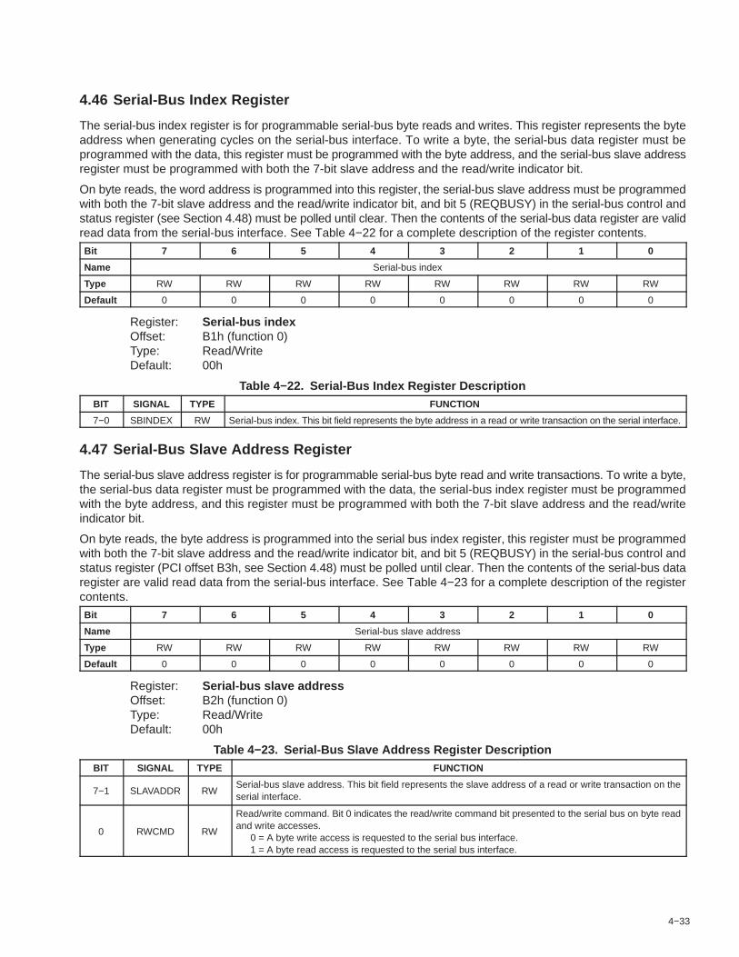
4−33
4.46 Serial-Bus Index Register
The serial-bus index register is for programmable serial-bus byte reads and writes. This register represents the byteaddress when generating cycles on the serial-bus interface. To write a byte, the serial-bus data register must beprogrammed with the data, this register must be programmed with the byte address, and the serial-bus slave addressregister must be programmed with both the 7-bit slave address and the read/write indicator bit.
On byte reads, the word address is programmed into this register, the serial-bus slave address must be programmedwith both the 7-bit slave address and the read/write indicator bit, and bit 5 (REQBUSY) in the serial-bus control andstatus register (see Section 4.48) must be polled until clear. Then the contents of the serial-bus data register are validread data from the serial-bus interface. See Table 4−22 for a complete description of the register contents.
Bit 7 6 5 4 3 2 1 0
Name Serial-bus index
Type RW RW RW RW RW RW RW RW
Default 0 0 0 0 0 0 0 0
Register: Serial-bus indexOffset: B1h (function 0)Type: Read/WriteDefault: 00h
Table 4−22. Serial-Bus Index Register DescriptionBIT SIGNAL TYPE FUNCTION
7−0 SBINDEX RW Serial-bus index. This bit field represents the byte address in a read or write transaction on the serial interface.
4.47 Serial-Bus Slave Address Register
The serial-bus slave address register is for programmable serial-bus byte read and write transactions. To write a byte,the serial-bus data register must be programmed with the data, the serial-bus index register must be programmedwith the byte address, and this register must be programmed with both the 7-bit slave address and the read/writeindicator bit.
On byte reads, the byte address is programmed into the serial bus index register, this register must be programmedwith both the 7-bit slave address and the read/write indicator bit, and bit 5 (REQBUSY) in the serial-bus control andstatus register (PCI offset B3h, see Section 4.48) must be polled until clear. Then the contents of the serial-bus dataregister are valid read data from the serial-bus interface. See Table 4−23 for a complete description of the registercontents.
Bit 7 6 5 4 3 2 1 0
Name Serial-bus slave address
Type RW RW RW RW RW RW RW RW
Default 0 0 0 0 0 0 0 0
Register: Serial-bus slave addressOffset: B2h (function 0)Type: Read/WriteDefault: 00h
Table 4−23. Serial-Bus Slave Address Register DescriptionBIT SIGNAL TYPE FUNCTION
7−1 SLAVADDR RWSerial-bus slave address. This bit field represents the slave address of a read or write transaction on theserial interface.
0 RWCMD RW
Read/write command. Bit 0 indicates the read/write command bit presented to the serial bus on byte readand write accesses.
0 = A byte write access is requested to the serial bus interface.1 = A byte read access is requested to the serial bus interface.

4−34
4.48 Serial-Bus Control and Status Register
The serial-bus control and status register communicates serial-bus status information and selects the quickcommand protocol. Bit 5 (REQBUSY) in this register must be polled during serial-bus byte reads to indicate whendata is valid in the serial-bus data register. See Table 4−24 for a complete description of the register contents.
Bit 7 6 5 4 3 2 1 0
Name Serial-bus control and status
Type RW R R R RC RW RC RC
Default 0 0 0 0 0 0 0 0
Register: Serial-bus control and statusOffset: B3h (function 0)Type: Read-only, Read/Write, Read/ClearDefault: 00h
Table 4−24. Serial-Bus Control and Status Register DescriptionBIT SIGNAL TYPE FUNCTION
7 PROT_SEL RWProtocol select. When bit 7 is set, the send-byte protocol is used on write requests and the receive-byteprotocol is used on read commands. The word-address byte in the serial-bus index register (PCI offset B1h,see Section 4.46) is not output by the PCI1520 when bit 7 is set.
6 RSVD R Reserved. Bit 6 returns 0 when read.
5 REQBUSY R
Requested serial-bus access busy. Bit 5 indicates that a requested serial-bus access (byte read or write)is in progress. A request is made, and bit 5 is set, by writing to the serial-bus slave address register (PCIoffset B2h, see Section 4.47). Bit 5 must be polled on reads from the serial interface. After the byte readaccess has been requested, the read data is valid in the serial-bus data register.
4 ROMBUSY R
Serial EEPROM busy status. Bit 4 indicates the status of the PCI1520 serial EEPROM circuitry. Bit 4 is setduring the loading of the subsystem ID and other default values from the serial-bus EEPROM.
0 = Serial EEPROM circuitry is not busy1 = Serial EEPROM circuitry is busy
3 SBDETECT RC
Serial-bus detect. When bit 3 is set, it indicates that the serial-bus interface is detected. A pulldown resistormust be implemented on the LATCH terminal for bit 3 to be set. If bit 3 is reset, then the MFUNC4 andMFUNC1 terminals can be used for alternate functions such as general-purpose inputs and outputs.
0 = Serial-bus interface not detected1 = Serial-bus interface detected
2 SBTEST RWSerial-bus test. When bit 2 is set, the serial-bus clock frequency is increased for test purposes.
0 = Serial-bus clock at normal operating frequency, 100 kHz (default)1 = Serial-bus clock frequency increased for test purposes
1 REQ_ERR RC
Requested serial-bus access error. Bit 1 indicates when a data error occurs on the serial interface duringa requested cycle, and can be set due to a missing acknowledge. Bit 1 is cleared by a writeback of 1.
0 = No error detected during user-requested byte read or write cycle1 = Data error detected during user-requested byte read or write cycle
0 ROM_ERR RC
EEPROM data-error status. Bit 0 indicates when a data error occurs on the serial interface during theauto-load from the serial-bus EEPROM, and can be set due to a missing acknowledge. Bit 0 is also set oninvalid EEPROM data formats. See Section 3.6.1, Serial Bus Interface Implementation, for details onEEPROM data format. Bit 0 is cleared by a writeback of 1.
0 = No error detected during auto-load from serial-bus EEPROM1 = Data error detected during auto-load from serial-bus EEPROM

5−1
5 ExCA Compatibility Registers (Functions 0 and 1)
The ExCA registers implemented in the PCI1520 are register-compatible with the Intel 82365SL−DF PCMCIAcontroller. ExCA registers are identified by an offset value that is compatible with the legacy I/O index/data schemeused on the Intel 82365 ISA controller. The ExCA registers are accessed through this scheme by writing the registeroffset value into the index register (I/O base) and reading or writing the data register (I/O base + 1). The I/O baseaddress used in the index/data scheme is programmed in the PC Card 16-bit I/F legacy-mode base address register(PCI offset 44h, see Section 4.28), which is shared by both card sockets. The offsets from this base address runcontiguously from 00h to 3Fh for socket A, and from 40h to 7Fh for socket B. See Figure 5−1 for an ExCA I/O mappingillustration.
CardBus Socket/ExCA Base Address
16-Bit Legacy-Mode Base Address
10h
44h
00h
3Fh
Offset
Index
Host I/O Space
Data
PC Card AExCA
Registers
PC Card BExCA
Registers
40h
7Fh
NOTE: The 16-bit legacy mode base address register is shared by functions 0 and 1 as indicated by the shading.
PCI1520 Configuration RegistersOffset
Figure 5−1. ExCA Register Access Through I/O
The TI PCI1520 also provides a memory-mapped alias of the ExCA registers by directly mapping them into PCImemory space. They are located through the CardBus socket/ExCA base-address register (PCI offset 10h, seeSection 4.12) at memory offset 800h. Each socket has a separate base address programmable by function. SeeFigure 5−2 for an ExCA memory mapping illustration. Note that memory offsets are 800h−844h for both functions0 and 1. This illustration also identifies the CardBus socket register mapping, which is mapped into the same 4-Kwindow at memory offset 00h.
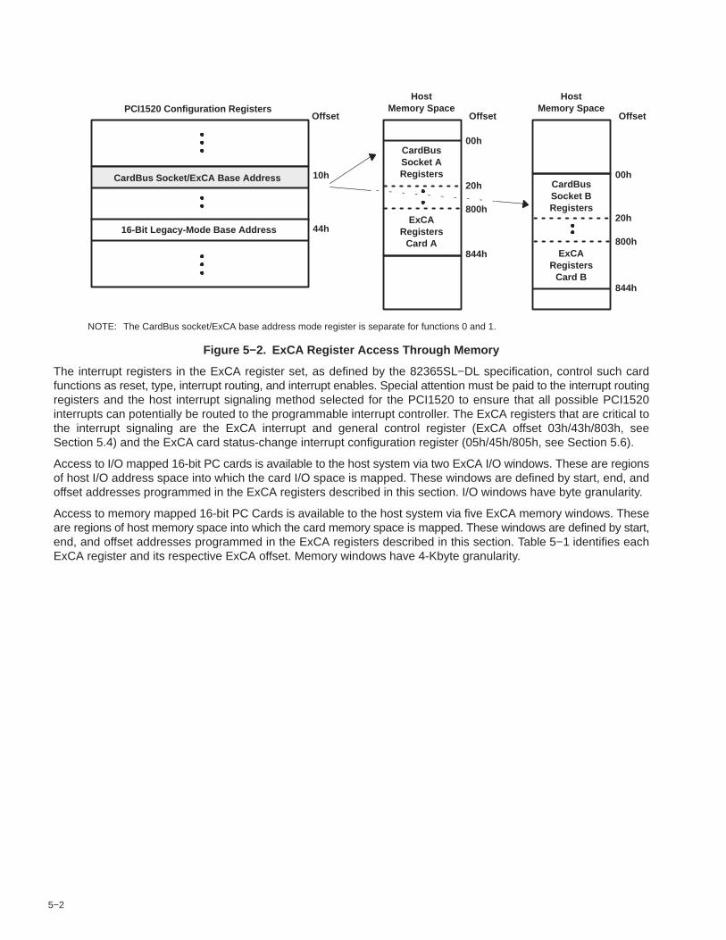
5−2
CardBus Socket/ExCA Base Address
16-Bit Legacy-Mode Base Address
10h
44h
NOTE: The CardBus socket/ExCA base address mode register is separate for functions 0 and 1.
PCI1520 Configuration Registers
CardBusSocket ARegisters
HostMemory Space
00h
ExCARegisters
Card A
20h
800h
844h
Offset
CardBusSocket BRegisters
HostMemory Space
00h
ExCARegisters
Card B
20h
800h
844h
OffsetOffset
Figure 5−2. ExCA Register Access Through Memory
The interrupt registers in the ExCA register set, as defined by the 82365SL−DL specification, control such cardfunctions as reset, type, interrupt routing, and interrupt enables. Special attention must be paid to the interrupt routingregisters and the host interrupt signaling method selected for the PCI1520 to ensure that all possible PCI1520interrupts can potentially be routed to the programmable interrupt controller. The ExCA registers that are critical tothe interrupt signaling are the ExCA interrupt and general control register (ExCA offset 03h/43h/803h, seeSection 5.4) and the ExCA card status-change interrupt configuration register (05h/45h/805h, see Section 5.6).
Access to I/O mapped 16-bit PC cards is available to the host system via two ExCA I/O windows. These are regionsof host I/O address space into which the card I/O space is mapped. These windows are defined by start, end, andoffset addresses programmed in the ExCA registers described in this section. I/O windows have byte granularity.
Access to memory mapped 16-bit PC Cards is available to the host system via five ExCA memory windows. Theseare regions of host memory space into which the card memory space is mapped. These windows are defined by start,end, and offset addresses programmed in the ExCA registers described in this section. Table 5−1 identifies eachExCA register and its respective ExCA offset. Memory windows have 4-Kbyte granularity.

5−3
Table 5−1. ExCA Registers and Offsets
EXCA REGISTER NAMEPCI MEMORY ADDRESS ExCA OFFSET (HEX)
EXCA REGISTER NAMEPCI MEMORY ADDRESS
OFFSET (HEX) CARD A CARD B
Identification and revision 800 00 40
Interface status 801 01 41
Power control 802 02 42
Interrupt and general control 803 03 43
Card status change 804 04 44
Card status-change interrupt configuration 805 05 45
Address window enable 806 06 46
I / O window control 807 07 47
I / O window 0 start-address low byte 808 08 48
I / O window 0 start-address high byte 809 09 49
I / O window 0 end-address low byte 80A 0A 4A
I / O window 0 end-address high byte 80B 0B 4B
I / O window 1 start-address low byte 80C 0C 4C
I / O window 1 start-address high byte 80D 0D 4D
I / O window 1 end-address low byte 80E 0E 4E
I / O window 1 end-address high byte 80F 0F 4F
Memory window 0 start-address low byte 810 10 50
Memory window 0 start-address high byte 811 11 51
Memory window 0 end-address low byte 812 12 52
Memory window 0 end-address high byte 813 13 53
Memory window 0 offset-address low byte 814 14 54
Memory window 0 offset-address high byte 815 15 55
Card detect and general control 816 16 56
Reserved 817 17 57
Memory window 1 start-address low byte 818 18 58
Memory window 1 start-address high byte 819 19 59
Memory window 1 end-address low byte 81A 1A 5A
Memory window 1 end-address high byte 81B 1B 5B
Memory window 1 offset-address low byte 81C 1C 5C
Memory window 1 offset-address high byte 81D 1D 5D
Global control 81E 1E 5E
Reserved 81F 1F 5F
Memory window 2 start-address low byte 820 20 60
Memory window 2 start-address high byte 821 21 61
Memory window 2 end-address low byte 822 22 62
Memory window 2 end-address high byte 823 23 63
Memory window 2 offset-address low byte 824 24 64
Memory window 2 offset-address high byte 825 25 65
Reserved 826 26 66
Reserved 827 27 67
Memory window 3 start-address low byte 828 28 68
Memory window 3 start-address high byte 829 29 69
Memory window 3 end-address low byte 82A 2A 6A

5−4
Table 5−1. ExCA Registers and Offsets (Continued)
EXCA REGISTER NAMEPCI MEMORY ADDRESS ExCA OFFSET (HEX)
EXCA REGISTER NAMEPCI MEMORY ADDRESS
OFFSET (HEX) CARD A CARD B
Memory window 3 end-address high byte 82B 2B 6B
Memory window 3 offset-address low byte 82C 2C 6C
Memory window 3 offset-address high byte 82D 2D 6D
Reserved 82E 2E 6E
Reserved 82F 2F 6F
Memory window 4 start-address low byte 830 30 70
Memory window 4 start-address high byte 831 31 71
Memory window 4 end-address low byte 832 32 72
Memory window 4 end-address high byte 833 33 73
Memory window 4 offset-address low byte 834 34 74
Memory window 4 offset-address high byte 835 35 75
I/O window 0 offset-address low byte 836 36 76
I/O window 0 offset-address high byte 837 37 77
I/O window 1 offset-address low byte 838 38 78
I/O window 1 offset-address high byte 839 39 79
Reserved 83A 3A 7A
Reserved 83B 3B 7B
Reserved 83C 3C 7C
Reserved 83D 3D 7D
Reserved 83E 3E 7E
Reserved 83F 3F 7F
Memory window page 0 840 − −
Memory window page 1 841 − −
Memory window page 2 842 − −
Memory window page 3 843 − −
Memory window page 4 844 − −
A bit description table, typically included when a register contains bits of more than one type or purpose, indicatesbit field names, which appear in the signal column; a detailed field description, which appears in the function column;and field access tags, which appear in the type column of the bit description table. Table 4−2 describes the fieldaccess tags.

5−5
5.1 ExCA Identification and Revision Register
The ExCA identification and revision register provides host software with information on 16-bit PC Card support andIntel 82365SL-DF compatibility. This register is read-only or read/write, depending on the setting of bit 5(SUBSYSRW) in the system control register (PCI offset 80h, see Section 4.29). See Table 5−2 for a completedescription of the register contents.
Bit 7 6 5 4 3 2 1 0
Name ExCA identification and revision
Type R R RW RW RW RW RW RW
Default 1 0 0 0 0 1 0 0
Register: ExCA identification and revisionOffset: CardBus socket address + 800h; Card A ExCA offset 00h
Card B ExCA offset 40hType: Read-only, Read/WriteDefault: 84h
Table 5−2. ExCA Identification and Revision Register DescriptionBIT SIGNAL TYPE FUNCTION
7−6 IFTYPE RInterface type. These bits, which are hardwired as 10b, identify the 16-bit PC Card support provided by thePCI1520. The PCI1520 supports both I/O and memory 16-bit PC cards.
5−4 RSVD RW Reserved. Bits 5 and 4 can be used for Intel 82365SL-DF emulation.
3−0 365REV RWIntel 82365SL-DF revision. This field stores the Intel 82365SL-DF revision supported by the PCI1520. Hostsoftware can read this field to determine compatibility to the Intel 82365SL-DF register set. Writing 0010b tothis field puts the controller in 82365SL mode.

5−6
5.2 ExCA Interface Status Register
The ExCA interface status register provides information on the current status of the PC Card interface. An X in thedefault bit value indicates that the value of the bit after reset depends on the state of the PC Card interface. SeeTable 5−3 for a complete description of the register contents.
Bit 7 6 5 4 3 2 1 0
Name ExCA interface status
Type R R R R R R R R
Default 0 0 X X X X X X
Register: ExCA interface statusOffset: CardBus socket address + 801h; Card A ExCA offset 01h
Card B ExCA offset 41hType: Read-onlyDefault: 00XX XXXXb
Table 5−3. ExCA Interface Status Register DescriptionBIT SIGNAL TYPE FUNCTION
7 RSVD R Reserved. Bit 7 returns 0 when read.
6 CARDPWR R
Card Power. Bit 6 indicates the current power status of the PC Card socket. This bit reflects how the ExCApower control register (ExCA offset 02h/42h/802h, see Section 5.3) is programmed. Bit 6 is encoded as:
0 = VCC and VPP to the socket turned off (default)1 = VCC and VPP to the socket turned on
5 READY RReady. Bit 5 indicates the current status of the READY signal at the PC Card interface.
0 = PC Card not ready for data transfer1 = PC Card ready for data transfer
4 CARDWP R
Card write protect (WP). Bit 4 indicates the current status of WP at the PC Card interface. This signal reportsto the PCI1520 whether or not the memory card is write protected. Furthermore, write protection for an entirePCI1520 16-bit memory window is available by setting the appropriate bit in the memory windowoffset-address high-byte register.
0 = WP is 0. PC Card is read/write.1 = WP is 1. PC Card is read-only.
3 CDETECT2 R
Card detect 2. Bit 3 indicates the status of CD2 at the PC Card interface. Software may use this and bit 2(CDETECT1) to determine if a PC Card is fully seated in the socket.
0 = CD2 is 1. No PC Card is inserted.1 = CD2 is 0. PC Card is at least partially inserted.
2 CDETECT1 R
Card detect 1. Bit 2 indicates the status of CD1 at the PC Card interface. Software may use this and bit 3(CDETECT2) to determine if a PC Card is fully seated in the socket.
0 = CD1 is 1. No PC Card is inserted.1 = CD1 is 0. PC Card is at least partially inserted.
1−0 BVDSTAT R
Battery voltage detect. When a 16-bit memory card is inserted, the field indicates the status of the batteryvoltage detect signals (BVD1, BVD2) at the PC Card interface, where bit 1 reflects the BVD2 status and bit 0reflects BVD1.
00 = Battery dead01 = Battery dead10 = Battery low; warning11 = Battery good
When a 16-bit I/O card is inserted, this field indicates the status of SPKR (bit 1) and STSCHG (bit 0) at thePC Card interface. In this case, the two bits in this field directly reflect the current state of these card outputs.

5−7
5.3 ExCA Power Control Register
The ExCA power control register provides PC Card power control. Bit 7 (COE) of this register controls the 16-bit outputenables on the socket interface, and can be used for power management in 16-bit PC Card applications. SeeTable 5−4 and Table 5−5 for a complete description of the register contents.
Bit 7 6 5 4 3 2 1 0
Name ExCA power control
Type RW R R RW RW R RW RW
Default 0 0 0 0 0 0 0 0
Register: ExCA power controlOffset: CardBus socket address + 802h; Card A ExCA offset 02h
Card B ExCA offset 42hType: Read-only, Read/WriteDefault: 00h
Table 5−4. ExCA Power Control Register Description—82365SL SupportBIT SIGNAL TYPE FUNCTION
7 COE RW
Card output enable. Bit 7 controls the state of all of the 16-bit outputs on the PCI1520. This bit isencoded as:
0 = 16-bit PC Card outputs disabled (default)1 = 16-bit PC Card outputs enabled
6 RSVD R Reserved. Bit 6 returns 0 when read.
5 AUTOPWRSWEN RWAuto power switch enable.
0 = Automatic socket power switching based on card detects is disabled.1 = Automatic socket power switching based on card detects is enabled.
4 CAPWREN RW
PC Card power enable.0 = VCC = No connection1 = VCC is enabled and controlled by bit 2 (EXCAPOWER) of the system control register
(PCI offset 80h, see Section 4.29).
3−2 RSVD R Reserved. Bits 3 and 2 return 0s when read.
1−0 EXCAVPP RW
PC Card VPP power control. Bits 1 and 0 are used to request changes to card VPP. The PCI1520 ignoresthis field unless VCC to the socket is enabled. This field is encoded as:
00 = No connection (default)01 = VCC10 = 12 V11 = Reserved
Table 5−5. ExCA Power Control Register Description—82365SL-DF SupportBIT SIGNAL TYPE FUNCTION
7 COE RWCard output enable. Bit 7 controls the state of all of the 16-bit outputs on the PCI1520. This bit is encoded as:
0 = 16-bit PC Card outputs disabled (default)1 = 16-bit PC Card outputs enabled
6−5 RSVD R Reserved. Bits 6 and 5 return 0s when read.
4−3 EXCAVCC RW
VCC. Bits 4 and 3 are used to request changes to card VCC. This field is encoded as:00 = 0 V (default)01 = 0 V reserved10 = 5 V11 = 3.3 V
2 RSVD R Reserved. Bit 2 returns 0 when read.
1−0 EXCAVPP RW
VPP. Bits 1 and 0 are used to request changes to card VPP. The PCI1520 ignores this field unless VCC tothe socket is enabled. This field is encoded as:
00 = No connection (default)01 = VCC10 = 12 V11 = Reserved

5−8
5.4 ExCA Interrupt and General Control Register
The ExCA interrupt and general control register controls interrupt routing for I/O interrupts, as well as other critical16-bit PC Card functions. See Table 5−6 for a complete description of the register contents.
Bit 7 6 5 4 3 2 1 0
Name ExCA interrupt and general control
Type RW RW RW RW RW RW RW RW
Default 0 0 0 0 0 0 0 0
Register: ExCA interrupt and general controlOffset: CardBus socket address + 803h; Card A ExCA offset 03h
Card B ExCA offset 43hType: Read/WriteDefault: 00h
Table 5−6. ExCA Interrupt and General Control Register DescriptionBIT SIGNAL TYPE FUNCTION
7 RINGEN RWCard ring indicate enable. Bit 7 enables the ring indicate function of BVD1/RI. This bit is encoded as:
0 = Ring indicate disabled (default)1 = Ring indicate enabled
6 RESET RW
Card reset. Bit 6 controls the 16-bit PC Card RESET, and allows host software to force a card reset. Bit 6affects 16-bit cards only. This bit is encoded as:
0 = RESET signal asserted (default)1 = RESET signal deasserted
5 CARDTYPE RWCard type. Bit 5 indicates the PC card type. This bit is encoded as:
0 = Memory PC Card installed (default)1 = I/O PC Card installed
4 CSCROUTE RW
PCI interrupt CSC routing enable bit. When bit 4 is set (high), the card status change interrupts are routedto PCI interrupts. When low, the card status change interrupts are routed using bits 7−4 (CSCSELECT field)in the ExCA card status-change interrupt configuration register (ExCA offset 05h/45h/805h, seeSection 5.6). This bit is encoded as:
0 = CSC interrupts are routed by ExCA registers (default).1 = CSC interrupts are routed to PCI interrupts.
3−0 INTSELECT RW
Card interrupt select for I/O PC Card functional interrupts. Bits 3−0 select the interrupt routing for I/OPC Card functional interrupts. This field is encoded as:
0000 = No interrupt routing (default). CSC interrupts are routed to PCI interrupts. This bit setting is ORed with bit 4 (CSCROUTE) for backward compatibility.
0001 = IRQ1 enabled0010 = SMI enabled0011 = IRQ3 enabled0100 = IRQ4 enabled0101 = IRQ5 enabled0100 = IRQ6 enabled0111 = IRQ7 enabled1000 = IRQ8 enabled1001 = IRQ9 enabled1010 = IRQ10 enabled1011 = IRQ11 enabled1100 = IRQ12 enabled1101 = IRQ13 enabled1110 = IRQ14 enabled1111 = IRQ15 enabled

5−9
5.5 ExCA Card Status-Change Register
The ExCA card status-change register controls interrupt routing for I/O interrupts as well as other critical 16-bit PCCard functions. The register enables these interrupt sources to generate an interrupt to the host. When the interruptsource is disabled, the corresponding bit in this register always reads 0. When an interrupt source is enabled, thecorresponding bit in this register is set to indicate that the interrupt source is active. After generating the interrupt tothe host, the interrupt service routine must read this register to determine the source of the interrupt. The interruptservice routine is responsible for resetting the bits in this register as well. Resetting a bit is accomplished by one oftwo methods: a read of this register or an explicit write back of 1 to the status bit. The choice of these two methodsis based on bit 2 (interrupt flag clear mode select) in the ExCA global control register (ExCA offset 1E/5E/81E, seeSection 5.20). See Table 5−7 for a complete description of the register contents.
Bit 7 6 5 4 3 2 1 0
Name ExCA card status-change
Type R R R R R R R R
Default 0 0 0 0 0 0 0 0
Register: ExCA card status-changeOffset: CardBus socket address + 804h; Card A ExCA offset 04h
Card B ExCA offset 44hType: Read-onlyDefault: 00h
Table 5−7. ExCA Card Status-Change Register DescriptionBIT SIGNAL TYPE FUNCTION
7−4 RSVD R Reserved. Bits 7−4 return 0s when read.
3 CDCHANGE R
Card detect change. Bit 3 indicates whether a change on CD1 or CD2 occurred at the PC Cardinterface. This bit is encoded as:
0 = No change detected on either CD1 or CD21 = Change detected on either CD1 or CD2
2 READYCHANGE R
Ready change. When a 16-bit memory is installed in the socket, bit 2 includes whether the source ofa PCI1520 interrupt was due to a change on READY at the PC Card interface, indicating that thePC Card is now ready to accept new data. This bit is encoded as:
0 = No low-to-high transition detected on READY (default)1 = Detected low-to-high transition on READY
When a 16-bit I/O card is installed, bit 2 is always 0.
1 BATWARN R
Battery warning change. When a 16-bit memory card is installed in the socket, bit 1 indicates whetherthe source of a PCI1520 interrupt was due to a battery-low warning condition. This bit is encoded as:
0 = No battery warning condition (default)1 = Detected battery warning condition
When a 16-bit I/O card is installed, bit 1 is always 0.
0 BATDEAD R
Battery dead or status change. When a 16-bit memory card is installed in the socket, bit 0 indicateswhether the source of a PCI1520 interrupt was due to a battery dead condition. This bit is encoded as:
0 = STSCHG deasserted (default)1 = STSCHG asserted
Ring indicate. When the PCI1520 is configured for ring indicate operation, bit 0 indicates the status ofRI.

5−10
5.6 ExCA Card Status-Change Interrupt Configuration Register
The ExCA card status-change interrupt configuration register controls interrupt routing for card status-changeinterrupts, as well as masking CSC interrupt sources. See Table 5−8 for a complete description of the registercontents.
Bit 7 6 5 4 3 2 1 0
Name ExCA status-change-interrupt configuration
Type RW RW RW RW RW RW RW RW
Default 0 0 0 0 0 0 0 0
Register: ExCA card status-change interrupt configurationOffset: CardBus socket address + 805h; Card A ExCA offset 05h
Card B ExCA offset 45hType: Read/WriteDefault: 00h
Table 5−8. ExCA Card Status-Change Interrupt Configuration Register DescriptionBIT SIGNAL TYPE FUNCTION
7−4 CSCSELECT RW
Interrupt select for card status change. Bits 7−4 select the interrupt routing for card status-changeinterrupts.
0000 = CSC interrupts routed to PCI interrupts if bit 5 (CSC) of the diagnostic register (PCI offset 93h, seeSection 4.34) is set to 1. In this case bit 4 (CSCROUTE) of the ExCA interrupt and general control register(ExCA offset 03h/43h/803h, see Section 5.4) is a don’t care. This is the default setting.
0000 = No ISA interrupt routing if bit 5 (CSC) of the diagnostic register is set to 0 (see Section 4.34). Inthis case, CSC interrupts are routed to PCI interrupts by setting bit 4 (CSCROUTE) of the ExCA interruptand general control register (ExCA offset 03h/43h/803h, see Section 5.4) to 1.
This field is encoded as:0000 = No interrupt routing (default) 1000 = IRQ8 enabled0001 = IRQ1 enabled 1001 = IRQ9 enabled0010 = SMI enabled 1010 = IRQ10 enabled0011 = IRQ3 enabled 1011 = IRQ11 enabled0100 = IRQ4 enabled 1100 = IRQ12 enabled0101 = IRQ5 enabled 1101 = IRQ13 enabled0110 = IRQ6 enabled 1110 = IRQ14 enabled0111 = IRQ7 enabled 1111 = IRQ15 enabled
3 CDEN RWCard detect enable. Bit 3 enables interrupts on CD1 or CD2 changes. This bit is encoded as:
0 = Disables interrupts on CD1 or CD2 line changes (default)1 = Enables interrupts on CD1 or CD2 line changes
2 READYEN RW
Ready enable. Bit 2 enables/disables a low-to-high transition on PC Card READY to generate a hostinterrupt. This interrupt source is considered a card status change. This bit is encoded as:
0 = Disables host interrupt generation (default)1 = Enables host interrupt generation
1 BATWARNEN RW
Battery warning enable. Bit 1 enables/disables a battery warning condition to generate a CSC interrupt.This bit is encoded as:
0 = Disables host interrupt generation (default)1 = Enables host interrupt generation
0 BATDEADEN RW
Battery dead enable. Bit 0 enables/disables a battery dead condition on a memory PC Card or assertionof the STSCHG I/O PC Card signal to generate a CSC interrupt.
0 = Disables host interrupt generation (default)1 = Enables host interrupt generation

5−11
5.7 ExCA Address Window Enable Register
The ExCA address window enable register enables/disables the memory and I/O windows to the 16-bit PC Card. Bydefault, all windows to the card are disabled. The PCI1520 does not acknowledge PCI memory or I/O cycles to thecard if the corresponding enable bit in this register is 0, regardless of the programming of the memory or I/O windowstart/end/offset address registers. See Table 5−9 for a complete description of the register contents.
Bit 7 6 5 4 3 2 1 0
Name ExCA address window enable
Type RW RW R RW RW RW RW RW
Default 0 0 0 0 0 0 0 0
Register: ExCA address window enableOffset: CardBus socket address + 806h; Card A ExCA offset 06h
Card B ExCA offset 46hType: Read-only, Read/WriteDefault: 00h
Table 5−9. ExCA Address Window Enable Register DescriptionBIT SIGNAL TYPE FUNCTION
7 IOWIN1EN RWI/O window 1 enable. Bit 7 enables/disables I/O window 1 for the PC Card. This bit is encoded as:
0 = I/O window 1 disabled (default)1 = I/O window 1 enabled
6 IOWIN0EN RWI/O window 0 enable. Bit 6 enables/disables I/O window 0 for the PC Card. This bit is encoded as:
0 = I/O window 0 disabled (default)1 = I/O window 0 enabled
5 RSVD R Reserved. Bit 5 returns 0 when read.
4 MEMWIN4EN RW
Memory window 4 enable. Bit 4 enables/disables memory window 4 for the PC Card. This bit isencoded as:
0 = Memory window 4 disabled (default)1 = Memory window 4 enabled
3 MEMWIN3EN RW
Memory window 3 enable. Bit 3 enables/disables memory window 3 for the PC Card. This bit isencoded as:
0 = Memory window 3 disabled (default)1 = Memory window 3 enabled
2 MEMWIN2EN RW
Memory window 2 enable. Bit 2 enables/disables memory window 2 for the PC Card. This bit isencoded as:
0 = Memory window 2 disabled (default)1 = Memory window 2 enabled
1 MEMWIN1EN RW
Memory window 1 enable. Bit 1 enables/disables memory window 1 for the PC Card. This bit isencoded as:
0 = Memory window 1 disabled (default)1 = Memory window 1 enabled
0 MEMWIN0EN RW
Memory window 0 enable. Bit 0 enables/disables memory window 0 for the PC Card. This bit isencoded as:
0 = Memory window 0 disabled (default)1 = Memory window 0 enabled

5−12
5.8 ExCA I/O Window Control Register
The ExCA I/O window control register contains parameters related to I/O window sizing and cycle timing. SeeTable 5−10 for a complete description of the register contents.
Bit 7 6 5 4 3 2 1 0
Name ExCA I/O window control
Type RW RW RW RW RW RW RW RW
Default 0 0 0 0 0 0 0 0
Register: ExCA I/O window controlOffset: CardBus socket address + 807h; Card A ExCA offset 07h
Card B ExCA offset 47hType: Read/WriteDefault: 00h
Table 5−10. ExCA I/O Window Control Register DescriptionBIT SIGNAL TYPE FUNCTION
7 WAITSTATE1 RW
I/O window 1 wait state. Bit 7 controls the I/O window 1 wait state for 16-bit I/O accesses. Bit 7 has no effecton 8-bit accesses. This wait-state timing emulates the ISA wait state used by the Intel 82365SL-DF. Thisbit is encoded as:
0 = 16-bit cycles have standard length (default).1 = 16-bit cycles are extended by one equivalent ISA wait state.
6 ZEROWS1 RW
I/O window 1 zero wait state. Bit 6 controls the I/O window 1 wait state for 8-bit I/O accesses. Bit 6 hasno effect on 16-bit accesses. This wait-state timing emulates the ISA wait state used by the Intel82365SL-DF. This bit is encoded as:
0 = 8-bit cycles have standard length (default).1 = 8-bit cycles are reduced to equivalent of three ISA cycles.
5 IOIS16W1 RW
I/O window 1 IOIS16 source. Bit 5 controls the I/O window 1 automatic data sizing feature that uses IOIS16from the PC Card to determine the data width of the I/O data transfer. This bit is encoded as:
0 = Window data width determined by DATASIZE1, bit 4 (default).1 = Window data width determined by IOIS16.
4 DATASIZE1 RW
I/O window 1 data size. Bit 4 controls the I/O window 1 data size. Bit 4 is ignored if bit 5 (IOSIS16W1) isset. This bit is encoded as:
0 = Window data width is 8 bits (default).1 = Window data width is 16 bits.
3 WAITSTATE0 RW
I/O window 0 wait state. Bit 3 controls the I/O window 0 wait state for 16-bit I/O accesses. Bit 3 has no effecton 8-bit accesses. This wait-state timing emulates the ISA wait state used by the Intel 82365SL-DF. Thisbit is encoded as:
0 = 16-bit cycles have standard length (default).1 = 16-bit cycles are extended by one equivalent ISA wait state.
2 ZEROWS0 RW
I/O window 0 zero wait state. Bit 2 controls the I/O window 0 wait state for 8-bit I/O accesses. Bit 2 hasno effect on 16-bit accesses. This wait-state timing emulates the ISA wait state used by the Intel82365SL-DF. This bit is encoded as:
0 = 8-bit cycles have standard length (default).1 = 8-bit cycles are reduced to equivalent of three ISA cycles.
1 IOIS16W0 RW
I/O window 0 IOIS16 source. Bit 1 controls the I/O window 0 automatic data sizing feature that uses IOIS16from the PC Card to determine the data width of the I/O data transfer. This bit is encoded as:
0 = Window data width is determined by DATASIZE0, bit 0 (default).1 = Window data width is determined by IOIS16.
0 DATASIZE0 RW
I/O window 0 data size. Bit 0 controls the I/O window 0 data size. Bit 0 is ignored if bit 1 (IOSIS16W0) isset. This bit is encoded as:
0 = Window data width is 8 bits (default).1 = Window data width is 16 bits.

5−13
5.9 ExCA I/O Windows 0 and 1 Start-Address Low-Byte Registers
These registers contain the low byte of the 16-bit I/O window start address for I/O windows 0 and 1. The 8 bits of theseregisters correspond to the lower 8 bits of the start address.
Bit 7 6 5 4 3 2 1 0
Name ExCA I/O windows 0 and 1 start-address low-byte
Type RW RW RW RW RW RW RW RW
Default 0 0 0 0 0 0 0 0
Register: ExCA I/O window 0 start-address low-byteOffset: CardBus socket address + 808h; Card A ExCA offset 08h
Card B ExCA offset 48hRegister: ExCA I/O window 1 start-address low-byteOffset: CardBus socket address + 80Ch; Card A ExCA offset 0Ch
Card B ExCA offset 4ChType: Read/WriteDefault: 00h
5.10 ExCA I/O Windows 0 and 1 Start-Address High-Byte Registers
These registers contain the high byte of the 16-bit I/O window start address for I/O windows 0 and 1. The 8 bits ofthese registers correspond to the upper 8 bits of the start address.
Bit 7 6 5 4 3 2 1 0
Name ExCA I/O windows 0 and 1 start-address high-byte
Type RW RW RW RW RW RW RW RW
Default 0 0 0 0 0 0 0 0
Register: ExCA I/O window 0 start-address high-byteOffset: CardBus socket address + 809h; Card A ExCA offset 09h
Card B ExCA offset 49hRegister: ExCA I/O window 1 start-address high-byteOffset: CardBus socket address + 80Dh; Card A ExCA offset 0Dh
Card B ExCA offset 4DhType: Read/writeDefault: 00h

5−14
5.11 ExCA I/O Windows 0 and 1 End-Address Low-Byte Registers
These registers contain the low byte of the 16-bit I/O window end address for I/O windows 0 and 1. The 8 bits of theseregisters correspond to the lower 8 bits of the end address.
Bit 7 6 5 4 3 2 1 0
Name ExCA I/O windows 0 and 1 end-address low-byte
Type RW RW RW RW RW RW RW RW
Default 0 0 0 0 0 0 0 0
Register: ExCA I/O window 0 end-address low-byteOffset: CardBus socket address + 80Ah; Card A ExCA offset 0Ah
Card B ExCA offset 4AhRegister: ExCA I/O window 1 end-address low-byteOffset: CardBus socket address + 80Eh; Card A ExCA offset 0Eh
Card B ExCA offset 4EhType: Read/WriteDefault: 00h
5.12 ExCA I/O Windows 0 and 1 End-Address High-Byte Registers
These registers contain the high byte of the 16-bit I/O window end address for I/O windows 0 and 1. The 8 bits of theseregisters correspond to the upper 8 bits of the end address.
Bit 7 6 5 4 3 2 1 0
Name ExCA I/O windows 0 and 1 end-address high-byte
Type RW RW RW RW RW RW RW RW
Default 0 0 0 0 0 0 0 0
Register: ExCA I/O window 0 end-address high-byteOffset: CardBus socket address + 80Bh; Card A ExCA offset 0Bh
Card B ExCA offset 4BhRegister: ExCA I/O window 1 end-address high-byteOffset: CardBus socket address + 80Fh; Card A ExCA offset 0Fh
Card B ExCA offset 4FhType: Read/writeDefault: 00h

5−15
5.13 ExCA Memory Windows 0−4 Start-Address Low-Byte Registers
These registers contain the low byte of the 16-bit memory window start address for memory windows 0, 1, 2, 3, and4. The 8 bits of these registers correspond to bits A19−A12 of the start address.
Bit 7 6 5 4 3 2 1 0
Name ExCA memory windows 0−4 start-address low-byte
Type RW RW RW RW RW RW RW RW
Default 0 0 0 0 0 0 0 0
Register: ExCA memory window 0 start-address low-byteOffset: CardBus socket address + 810h; Card A ExCA offset 10h
Card B ExCA offset 50hRegister: ExCA memory window 1 start-address low-byteOffset: CardBus socket address + 818h; Card A ExCA offset 18h
Card B ExCA offset 58hRegister: ExCA memory window 2 start-address low-byteOffset: CardBus socket address + 820h; Card A ExCA offset 20h
Card B ExCA offset 60hRegister: ExCA memory window 3 start-address low-byteOffset: CardBus socket address + 828h; Card A ExCA offset 28h
Card B ExCA offset 68hRegister: ExCA memory window 4 start-address low-byteOffset: CardBus socket address + 830h; Card A ExCA offset 30h
Card B ExCA offset 70hType: Read/WriteDefault: 00h

5−16
5.14 ExCA Memory Windows 0−4 Start-Address High-Byte Registers
These registers contain the high nibble of the 16-bit memory window start address for memory windows 0, 1, 2, 3,and 4. The lower 4 bits of these registers correspond to bits A23−A20 of the start address. In addition, the memorywindow data width and wait states are set in this register. See Table 5−11 for a complete description of the registercontents.
Bit 7 6 5 4 3 2 1 0
Name ExCA memory windows 0−4 start-address high-byte
Type RW RW RW RW RW RW RW RW
Default 0 0 0 0 0 0 0 0
Register: ExCA memory window 0 start-address high-byteOffset: CardBus socket address + 811h; Card A ExCA offset 11h
Card B ExCA offset 51hRegister: ExCA memory window 1 start-address high-byteOffset: CardBus socket address + 819h; Card A ExCA offset 19h
Card B ExCA offset 59hRegister: ExCA memory window 2 start-address high-byteOffset: CardBus socket address + 821h; Card A ExCA offset 21h
Card B ExCA offset 61hRegister: ExCA memory window 3 start-address high-byteOffset: CardBus socket address + 829h; Card A ExCA offset 29h
Card B ExCA offset 69hRegister: ExCA memory window 4 start-address high-byteOffset: CardBus socket address + 831h; Card A ExCA offset 31h
Card B ExCA offset 71hType: Read/WriteDefault: 00h
Table 5−11. ExCA Memory Windows 0−4 Start-Address High-Byte Registers DescriptionBIT SIGNAL TYPE FUNCTION
7 DATASIZE RWData size. Bit 7 controls the memory window data width. This bit is encoded as:
0 = Window data width is 8 bits (default).1 = Window data width is 16 bits.
6 ZEROWAIT RW
Zero wait state. Bit 6 controls the memory window wait state for 8- and 16-bit accesses. This wait-state timingemulates the ISA wait state used by the Intel 82365SL-DF. This bit is encoded as:
0 = 8- and 16-bit cycles have standard length (default).1 = 8-bit cycles are reduced to equivalent of three ISA cycles.
16-bit cycles are reduced to equivalent of two ISA cycles.
5−4 SCRATCH RW Scratch pad bits. Bits 5 and 4 have no effect on memory window operation.
3−0 STAHN RWStart-address high nibble. Bits 3−0 represent the upper address bits A23−A20 of the memory windowstart address.

5−17
5.15 ExCA Memory Windows 0−4 End-Address Low-Byte Registers
These registers contain the low byte of the 16-bit memory window end address for memory windows 0, 1, 2, 3, and4. The 8 bits of these registers correspond to bits A19−A12 of the end address.
Bit 7 6 5 4 3 2 1 0
Name ExCA memory windows 0−4 end-address low-byte
Type RW RW RW RW RW RW RW RW
Default 0 0 0 0 0 0 0 0
Register: ExCA memory window 0 end-address low-byteOffset: CardBus socket address + 812h; Card A ExCA offset 12h
Card B ExCA offset 52hRegister: ExCA memory window 1 end-address low-byteOffset: CardBus socket address + 81Ah; Card A ExCA offset 1Ah
Card B ExCA offset 5AhRegister: ExCA memory window 2 end-address low-byteOffset: CardBus socket address + 822h; Card A ExCA offset 22h
Card B ExCA offset 62hRegister: ExCA memory window 3 end-address low-byteOffset: CardBus socket address + 82Ah; Card A ExCA offset 2Ah
Card B ExCA offset 6AhRegister: ExCA memory window 4 end-address low-byteOffset: CardBus socket address + 832h; Card A ExCA offset 32h
Card B ExCA offset 72hType: Read/WriteDefault: 00h

5−18
5.16 ExCA Memory Windows 0−4 End-Address High-Byte Registers
These registers contain the high nibble of the 16-bit memory window end address for memory windows 0, 1, 2, 3,and 4. The lower 4 bits of these registers correspond to bits A23−A20 of the end address. In addition, the memorywindow wait states are set in this register. See Table 5−12 for a complete description of the register contents.
Bit 7 6 5 4 3 2 1 0
Name ExCA memory windows 0−4 end-address high-byte
Type RW RW R R RW RW RW RW
Default 0 0 0 0 0 0 0 0
Register: ExCA memory window 0 end-address high-byteOffset: CardBus socket address + 813h; Card A ExCA offset 13h
Card B ExCA offset 53hRegister: ExCA memory window 1 end-address high-byteOffset: CardBus socket address + 81Bh; Card A ExCA offset 1Bh
Card B ExCA offset 5BhRegister: ExCA memory window 2 end-address high-byteOffset: CardBus socket address + 823h; Card A ExCA offset 23h
Card B ExCA offset 63hRegister: ExCA memory window 3 end-address high-byteOffset: CardBus socket address + 82Bh; Card A ExCA offset 2Bh
Card B ExCA offset 6BhRegister: ExCA memory window 4 end-address high-byteOffset: CardBus socket address + 833h; Card A ExCA offset 33h
Card B ExCA offset 73hType: Read-only, Read/WriteDefault: 00h
Table 5−12. ExCA Memory Windows 0−4 End-Address High-Byte Registers DescriptionBIT SIGNAL TYPE FUNCTION
7−6 MEMWS RWWait state. Bits 7 and 6 specify the number of equivalent ISA wait states to be added to 16-bit memoryaccesses. The number of wait states added is equal to the binary value of these two bits.
5−4 RSVD R Reserved. Bits 5 and 4 return 0s when read.
3−0 ENDHN RWEnd-address high nibble. Bits 3−0 represent the upper address bits A23−A20 of the memory window endaddress.

5−19
5.17 ExCA Memory Windows 0−4 Offset-Address Low-Byte Registers
These registers contain the low byte of the 16-bit memory window offset address for memory windows 0, 1, 2, 3, and4. The 8 bits of these registers correspond to bits A19−A12 of the offset address.
Bit 7 6 5 4 3 2 1 0
Name ExCA memory windows 0−4 offset-address low-byte
Type RW RW RW RW RW RW RW RW
Default 0 0 0 0 0 0 0 0
Register: ExCA memory window 0 offset-address low-byteOffset: CardBus socket address + 814h; Card A ExCA offset 14h
Card B ExCA offset 54hRegister: ExCA memory window 1 offset-address low-byteOffset: CardBus socket address + 81Ch; Card A ExCA offset 1Ch
Card B ExCA offset 5ChRegister: ExCA memory window 2 offset-address low-byteOffset: CardBus socket address + 824h; Card A ExCA offset 24h
Card B ExCA offset 64hRegister: ExCA memory window 3 offset-address low-byteOffset: CardBus socket address + 82Ch; Card A ExCA offset 2Ch
Card B ExCA offset 6ChRegister: ExCA memory window 4 offset-address low-byteOffset: CardBus socket address + 834h; Card A ExCA offset 34h
Card B ExCA offset 74hType: Read/WriteDefault: 00h

5−20
5.18 ExCA Memory Windows 0−4 Offset-Address High-Byte Registers
These registers contain the high 6 bits of the 16-bit memory window offset address for memory windows 0, 1, 2, 3,and 4. The lower 6 bits of these registers correspond to bits A25−A20 of the offset address. In addition, the writeprotection and common/attribute memory configurations are set in this register. See Table 5−13 for a completedescription of the register contents.
Bit 7 6 5 4 3 2 1 0
Name ExCA memory windows 0−4 offset-address high-byte
Type RW RW RW RW RW RW RW RW
Default 0 0 0 0 0 0 0 0
Register: ExCA memory window 0 offset-address high-byteOffset: CardBus socket address + 815h; Card A ExCA offset 15h
Card B ExCA offset 55hRegister: ExCA memory window 1 offset-address high-byteOffset: CardBus socket address + 81Dh; Card A ExCA offset 1Dh
Card B ExCA offset 5DhRegister: ExCA memory window 2 offset-address high-byteOffset: CardBus socket address + 825h; Card A ExCA offset 25h
Card B ExCA offset 65hRegister: ExCA memory window 3 offset-address high-byteOffset: CardBus socket address + 82Dh; Card A ExCA offset 2Dh
Card B ExCA offset 6DhRegister: ExCA memory window 4 offset-address high-byteOffset: CardBus socket address + 835h; Card A ExCA offset 35h
Card B ExCA offset 75hType: Read/WriteDefault: 00h
Table 5−13. ExCA Memory Windows 0−4 Offset-Address High-Byte Registers DescriptionBIT SIGNAL TYPE FUNCTION
7 WINWP RW
Write protect. Bit 7 specifies whether write operations to this memory window are enabled. This bit isencoded as:
0 = Write operations are allowed (default).1 = Write operations are not allowed.
6 REG RW
Bit 6 specifies whether this memory window is mapped to card attribute or common memory. This bit is encodedas:
0 = Memory window is mapped to common memory (default).1 = Memory window is mapped to attribute memory.
5−0 OFFHB RWOffset-address high byte. Bits 5−0 represent the upper address bits A25−A20 of the memory windowoffset address.

5−21
5.19 ExCA Card Detect and General Control Register
The ExCA card detect and general control register controls how the ExCA registers for the socket respond to cardremoval, as well as reports the status of VS1 and VS2 at the PC Card interface. See Table 5−14 for a completedescription of the register contents.
Bit 7 6 5 4 3 2 1 0
Name ExCA I/O card detect and general control
Type R R RW RW R R RW R
Default X X 0 0 0 0 0 0
Register: ExCA card detect and general controlOffset: CardBus socket address + 816h; Card A ExCA offset 16h
Card B ExCA offset 56hType: Read-only, Read/WriteDefault: XX00 0000b
Table 5−14. ExCA Card Detect and General Control Register DescriptionBIT SIGNAL TYPE FUNCTION
7 VS2STAT R
VS2 state. Bit 7 reports the current state of VS2 at the PC Card interface and, therefore, does not havea default value.
0 = VS2 low1 = VS2 high
6 VS1STAT R
VS1 state. Bit 6 reports the current state of VS1 at the PC Card interface and, therefore, does not havea default value.
0 = VS1 low1 = VS1 high
5 SWCSC RW
Software card detect interrupt. If bit 3 (CDEN) in the ExCA card status-change interrupt configurationregister (ExCA offset 05h/45h/805, see Section 5.6) is set, then writing a 1 to bit 5 causes a card-detectcard-status change interrupt for the associated card socket. If bit 3 (CDEN) in the ExCA cardstatus-change-interrupt configuration register (ExCA offset 05h/45h/805, see Section 5.6) is cleared to 0,then writing a 1 to bit 5 has no effect. A read operation of this bit always returns 0.
4 CDRESUME RW
Card detect resume enable. If bit 4 is set to 1, then once a card detect change has been detected on CD1and CD2 inputs, RI_OUT goes from high to low. RI_OUT remains low until bit 0 (card status change) inthe ExCA card status-change register is cleared (see Section 5.5). If this bit is a 0, then the card detectresume functionality is disabled.
0 = Card detect resume disabled (default)1 = Card detect resume enabled
3−2 RSVD R Reserved. Bits 3 and 2 return 0s when read.
1 REGCONFIG RW
Register configuration on card removal. Bit 1 controls how the ExCA registers for the socket react to a cardremoval event. This bit is encoded as:
0 = No change to ExCA registers on card removal (default)1 = Reset ExCA registers on card removal
0 RSVD R Reserved. Bit 0 returns 0 when read.

5−22
5.20 ExCA Global Control Register
The ExCA global control register controls both PC Card sockets and is not duplicated for each socket. The hostinterrupt mode bits in this register are retained for Intel 82365SL-DF compatibility. See Table 5−15 for a completedescription of the register contents.
Bit 7 6 5 4 3 2 1 0
Name ExCA global control
Type R R R RW RW RW RW RW
Default 0 0 0 0 0 0 0 0
Register: ExCA global controlOffset: CardBus socket address + 81Eh; Card A ExCA offset 1Eh
Card B ExCA offset 5EhType: Read-only, Read/WriteDefault: 00h
Table 5−15. ExCA Global Control Register DescriptionBIT SIGNAL TYPE FUNCTION
7−5 RSVD R Reserved. Bits 7−5 return 0s when read.
4 INTMODEB RW
Level/edge interrupt mode select − card B. Bit 4 selects the signaling mode for the PCI1520 host interruptfor card B interrupts. This bit is encoded as:
0 = Host interrupt is edge mode (default).1 = Host interrupt is level mode.
3 INTMODEA RW
Level/edge interrupt mode select − card A. Bit 3 selects the signaling mode for the PCI1520 host interruptfor card A interrupts. This bit is encoded as:
0 = Host interrupt is edge mode (default).1 = Host interrupt is level mode.
2 IFCMODE RW
Interrupt flag clear mode select. Bit 2 selects the interrupt flag clear mechanism for the flags in the ExCAcard status change register (ExCA offset 04h/44h/804h, see Section 5.5). This bit is encoded as:
0 = Interrupt flags are cleared by read of CSC register (default).1 = Interrupt flags are cleared by explicit writeback of 1.
1 CSCMODE RW
Card status change level/edge mode select. Bit 1 selects the signaling mode for the PCI1520 host interruptfor card status changes. This bit is encoded as:
0 = Host interrupt is edge mode (default).1 = Host interrupt is level mode.
0 PWRDWN RW
Power-down mode select. When bit 0 is set to 1, the PCI1520 is in power-down mode. In power-down mode,the PCI1520 card outputs are high-impedance until an active cycle is executed on the card interface.Following an active cycle, the outputs are again high-impedance. The PCI1520 still receives functionalinterrupts and/or card status-change interrupts; however, an actual card access is required to wake up theinterface. This bit is encoded as:
0 = Power-down mode is disabled (default).1 = Power-down mode is enabled.

5−23
5.21 ExCA I/O Windows 0 and 1 Offset-Address Low-Byte Registers
These registers contain the low byte of the 16-bit I/O window offset address for I/O windows 0 and 1. The 8 bits ofthese registers correspond to the lower 8 bits of the offset address, and bit 0 is always 0.
Bit 7 6 5 4 3 2 1 0
Name ExCA I/O windows 0 and 1 offset-address low-byte
Type RW RW RW RW RW RW RW R
Default 0 0 0 0 0 0 0 0
Register: ExCA I/O window 0 offset-address low-byteOffset: CardBus socket address + 836h; Card A ExCA offset 36h
Card B ExCA offset 76hRegister: ExCA I/O window 1 offset-address low-byteOffset: CardBus socket address + 838h; Card A ExCA offset 38h
Card B ExCA offset 78hType: Read-only, Read/WriteDefault: 00h
5.22 ExCA I/O Windows 0 and 1 Offset-Address High-Byte Registers
These registers contain the high byte of the 16-bit I/O window offset address for I/O windows 0 and 1. The 8 bits ofthese registers correspond to the upper 8 bits of the offset address.
Bit 7 6 5 4 3 2 1 0
Name ExCA I/O windows 0 and 1 offset-address high-byte
Type RW RW RW RW RW RW RW RW
Default 0 0 0 0 0 0 0 0
Register: ExCA I/O window 0 offset-address high-byteOffset: CardBus socket address + 837h; Card A ExCA offset 37h
Card B ExCA offset 77hRegister: ExCA I/O window 1 offset-address high-byteOffset: CardBus socket address + 839h; Card A ExCA offset 39h
Card B ExCA offset 79hType: Read/WriteDefault: 00h

5−24
5.23 ExCA Memory Windows 0−4 Page Registers
The upper 8 bits of a 4-byte PCI memory address are compared to the contents of this register when decodingaddresses for 16-bit memory windows. Each window has its own page register, all of which default to 00h. Byprogramming this register to a nonzero value, host software can locate 16-bit memory windows in any 1 of 25616-Mbyte regions in the 4-Gbyte PCI address space. These registers are only accessible when the ExCA registersare memory-mapped; that is, these registers cannot be accessed using the index/data I/O scheme.
Bit 7 6 5 4 3 2 1 0
Name ExCA memory windows 0−4 page
Type RW RW RW RW RW RW RW RW
Default 0 0 0 0 0 0 0 0
Register: ExCA memory windows 0−4 pageOffset: CardBus socket address + 840h, 841h, 842h, 843h, 844hType: Read/WriteDefault: 00h

6−1
6 CardBus Socket Registers (Functions 0 and 1)
The 1997 PC Card Standard requires a CardBus socket controller to provide five 32-bit registers that report andcontrol socket-specific functions. The PCI1520 provides the CardBus socket/ExCA base-address register (PCI offset10h, see Section 4.12) to locate these CardBus socket registers in PCI memory address space. Each socket has aseparate base address register for accessing the CardBus socket registers (see Figure 6−1). Table 6−1 gives thelocation of the socket registers in relation to the CardBus socket/ExCA base address.
The PCI1520 implements an additional register at offset 20h that provides power management control for the socket.
CardBus Socket/ExCA Base Address
16-Bit Legacy-Mode Base Address
10h
44h
NOTE: The CardBus socket/ExCA base address mode register is separate for functions 0 and 1.
PCI1520 Configuration Registers
CardBusSocket ARegisters
HostMemory Space
00h
ExCARegisters
Card A
20h
800h
844h
Offset
CardBusSocket BRegisters
HostMemory Space
00h
ExCARegisters
Card B
20h
800h
844h
Offse tOffset
Figure 6−1. Accessing CardBus Socket Registers Through PCI Memory
Table 6−1. CardBus Socket RegistersREGISTER NAME OFFSET
Socket event 00h
Socket mask 04h
Socket present-state 08h
Socket force event 0Ch
Socket control 10h
Reserved 14h−1Ch
Socket power-management 20h
A bit description table, typically included when a register contains bits of more than one type or purpose, indicatesbit field names, which appear in the signal column; a detailed field description, which appears in the function column;and field access tags, which appear in the type column of the bit description table. Table 4−2 describes the fieldaccess tags.

6−2
6.1 Socket Event Register
The socket event register indicates a change in socket status has occurred. These bits do not indicate what thechange is, only that one has occurred. Software must read the socket present-state register (CB offset 08h, seeSection 6.3) for current status. Each bit in this register can be cleared by writing a 1 to that bit. The bits in this registercan be set to a 1 by software by writing a 1 to the corresponding bit in the socket force event register (CB offset 0Ch,see Section 6.4). All bits in this register are cleared by PCI reset. They can be immediately set again, if, when comingout of PC Card reset, the bridge finds the status unchanged (that is, CSTSCHG reasserted or card detect is still true).Software must clear this register before enabling interrupts. If it is not cleared when interrupts are enabled, then aninterrupt is generated (but not masked) based on any bit set. See Table 6−2 for a complete description of the registercontents.
Bit 31 30 29 28 27 26 25 24 23 22 21 20 19 18 17 16
Name Socket event
Type R R R R R R R R R R R R R R R R
Default 0 0 0 0 0 0 0 0 0 0 0 0 0 0 0 0
Bit 15 14 13 12 11 10 9 8 7 6 5 4 3 2 1 0
Name Socket event
Type R R R R R R R R R R R R R/C R/C R/C R/C
Default 0 0 0 0 0 0 0 0 0 0 0 0 0 0 0 0
Register: Socket eventOffset: CardBus socket address + 00hType: Read-only, Read/Write, Read/ClearDefault: 0000 0000h
Table 6−2. Socket Event Register DescriptionBIT SIGNAL TYPE FUNCTION
31−4 RSVD R Reserved. Bits 31−4 return 0s when read.
3 PWREVENT R/CPower cycle. Bit 3 is set when the PCI1520 detects that bit 3 (PWRCYCLE) in the socket present-stateregister (CB offset 08h, see Section 6.3) has changed state. This bit is cleared by writing a 1.
2 CD2EVENT R/CCCD2. Bit 2 is set when the PCI1520 detects that bit 2 (CDETECT2) in the socket present-state register(CB offset 08h, see Section 6.3) has changed state. This bit is cleared by writing a 1.
1 CD1EVENT R/CCCD1. Bit 1 is set when the PCI1520 detects that bit 1 (CDETECT1) in the socket present-state register(CB offset 08h, see Section 6.3) has changed state. This bit is cleared by writing a 1.
0 CSTSEVENT R/CCSTSCHG. Bit 0 is set when bit 0 (CARDSTS) in the socket present-state register (CB offset 08h, seeSection 6.3) has changed state. For CardBus cards, bit 0 is set on the rising edge of CSTSCHG. For 16-bitPC Cards, bit 0 is set on both transitions of CSTSCHG. This bit is reset by writing a 1.

6−3
6.2 Socket Mask Register
The socket mask register allows software to control the CardBus card events that generate a status change interrupt.The state of these mask bits does not prevent the corresponding bits from reacting in the socket event register (CBoffset 00h, see Section 6.1). See Table 6−3 for a complete description of the register contents.
Bit 31 30 29 28 27 26 25 24 23 22 21 20 19 18 17 16
Name Socket mask
Type R R R R R R R R R R R R R R R R
Default 0 0 0 0 0 0 0 0 0 0 0 0 0 0 0 0
Bit 15 14 13 12 11 10 9 8 7 6 5 4 3 2 1 0
Name Socket mask
Type R R R R R R R R R R R R RW RW RW RW
Default 0 0 0 0 0 0 0 0 0 0 0 0 0 0 0 0
Register: Socket maskOffset: CardBus socket address + 04hType: Read-only, Read/WriteDefault: 0000 0000h
Table 6−3. Socket Mask Register DescriptionBIT SIGNAL TYPE FUNCTION
31−4 RSVD R Reserved. Bits 31−4 return 0s when read.
3 PWRMASK RW
Power cycle. Bit 3 masks bit 3 (PWRCYCLE) in the socket present-state register (CB offset 08h, seeSection 6.3) from causing a status change interrupt.
0 = PWRCYCLE event does not cause CSC interrupt (default).1 = PWRCYCLE event causes CSC interrupt.
2−1 CDMASK RW
Card detect mask. Bits 2 and 1 mask bits 1 and 2 (CDETECT1 and CDETECT2) in the socket present-stateregister (CB offset 08h, see Section 6.3) from causing a CSC interrupt.
00 = Insertion/removal does not cause CSC interrupt (default).01 = Reserved (undefined)10 = Reserved (undefined)11 = Insertion/removal causes CSC interrupt.
0 CSTSMASK RW
CSTSCHG mask. Bit 0 masks bit 0 (CARDSTS) in the socket present-state register (CB offset 08h, seeSection 6.3) from causing a CSC interrupt.
0 = CARDSTS event does not cause CSC interrupt (default).1 = CARDSTS event causes CSC interrupt.
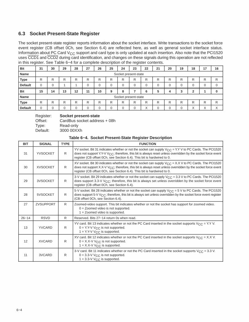
6−4
6.3 Socket Present-State Register
The socket present-state register reports information about the socket interface. Write transactions to the socket forceevent register (CB offset 0Ch, see Section 6.4) are reflected here, as well as general socket interface status.Information about PC Card VCC support and card type is only updated at each insertion. Also note that the PCI1520uses CCD1 and CCD2 during card identification, and changes on these signals during this operation are not reflectedin this register. See Table 6−4 for a complete description of the register contents.
Bit 31 30 29 28 27 26 25 24 23 22 21 20 19 18 17 16
Name Socket present-state
Type R R R R R R R R R R R R R R R R
Default 0 0 1 1 0 0 0 0 0 0 0 0 0 0 0 0
Bit 15 14 13 12 11 10 9 8 7 6 5 4 3 2 1 0
Name Socket present-state
Type R R R R R R R R R R R R R R R R
Default 0 0 0 0 0 0 0 0 0 X 0 0 0 X X X
Register: Socket present-stateOffset: CardBus socket address + 08hType: Read-onlyDefault: 3000 00XXh
Table 6−4. Socket Present-State Register DescriptionBIT SIGNAL TYPE FUNCTION
31 YVSOCKET RYV socket. Bit 31 indicates whether or not the socket can supply VCC = Y.Y V to PC Cards. The PCI1520does not support Y.Y-V VCC; therefore, this bit is always reset unless overridden by the socket force eventregister (CB offset 0Ch, see Section 6.4). This bit is hardwired to 0.
30 XVSOCKET RXV socket. Bit 30 indicates whether or not the socket can supply VCC = X.X V to PC Cards. The PCI1520does not support X.X-V VCC; therefore, this bit is always reset unless overridden by the socket force eventregister (CB offset 0Ch, see Section 6.4). This bit is hardwired to 0.
29 3VSOCKET R3-V socket. Bit 29 indicates whether or not the socket can supply VCC = 3.3 V to PC Cards. The PCI1520does support 3.3-V VCC; therefore, this bit is always set unless overridden by the socket force eventregister (CB offset 0Ch, see Section 6.4).
28 5VSOCKET R5-V socket. Bit 28 indicates whether or not the socket can supply VCC = 5 V to PC Cards. The PCI1520does support 5-V VCC; therefore, this bit is always set unless overridden by the socket force event register(CB offset 0Ch, see Section 6.4).
27 ZVSUPPORT R Zoomed-video support. This bit indicates whether or not the socket has support for zoomed video.0 = Zoomed video is not supported.1 = Zoomed video is supported.
26−14 RSVD R Reserved. Bits 27−14 return 0s when read.
13 YVCARD RYV card. Bit 13 indicates whether or not the PC Card inserted in the socket supports VCC = Y.Y V.
0 = Y.Y-V VCC is not supported.1 = Y.Y-V VCC is supported.
12 XVCARD RXV card. Bit 12 indicates whether or not the PC Card inserted in the socket supports VCC = X.X V.
0 = X.X-V VCC is not supported.1 = X.X-V VCC is supported.
11 3VCARD R3-V card. Bit 11 indicates whether or not the PC Card inserted in the socket supports VCC = 3.3 V.
0 = 3.3-V VCC is not supported.1 = 3.3-V VCC is supported.

6−5
Table 6−4. Socket Present-State Register (Continued)BIT SIGNAL TYPE FUNCTION
10 5VCARD R5-V card. Bit 10 indicates whether or not the PC Card inserted in the socket supports VCC = 5 V.
0 = 5-V VCC is not supported.1 = 5-V VCC is supported.
9 BADVCCREQ R
Bad VCC request. Bit 9 indicates that the host software has requested that the socket be powered at aninvalid voltage.
0 = Normal operation (default)1 = Invalid VCC request by host software
8 DATALOST R
Data lost. Bit 8 indicates that a PC Card removal event may have caused lost data because the cycle didnot terminate properly or because write data still resides in the PCI1520.
0 = Normal operation (default)1 = Potential data loss due to card removal
7 NOTACARD R
Not a card. Bit 7 indicates that an unrecognizable PC Card has been inserted in the socket. This bit is notupdated until a valid PC Card is inserted into the socket.
0 = Normal operation (default)1 = Unrecognizable PC Card detected
6 IREQCINT RREADY(IREQ)//CINT. Bit 6 indicates the current status of READY(IREQ)//CINT at the PC Card interface.
0 = READY(IREQ)//CINT low1 = READY(IREQ)//CINT high
5 CBCARD RCardBus card detected. Bit 5 indicates that a CardBus PC Card is inserted in the socket. This bit is notupdated until another card interrogation sequence occurs (card insertion).
4 16BITCARD R16-bit card detected. Bit 4 indicates that a 16-bit PC Card is inserted in the socket. This bit is not updateduntil another card interrogation sequence occurs (card insertion).
3 PWRCYCLE RPower cycle. Bit 3 indicates the status of each card powering request. This bit is encoded as:
0 = Socket powered down (default)1 = Socket powered up
2 CDETECT2 R
CCD2. Bit 2 reflects the current status of CCD2 at the PC Card interface. Changes to this signal duringcard interrogation are not reflected here.
0 = CCD2 low (PC Card may be present)1 = CCD2 high (PC Card not present)
1 CDETECT1 R
CCD1. Bit 1 reflects the current status of CCD1 at the PC Card interface. Changes to this signal duringcard interrogation are not reflected here.
0 = CCD1 low (PC Card may be present)1 = CCD1 high (PC Card not present)
0 CARDSTS RCSTSCHG. Bit 0 reflects the current status of CSTSCHG at the PC Card interface.
0 = CSTSCHG low1 = CSTSCHG high

6−6
6.4 Socket Force Event Register
The socket force event register is used to force changes to the socket event register (CB offset 00h, see Section 6.1)and the socket present-state register (see Section 6.3). Bit 14 (CVSTEST) in this register must be written whenforcing changes that require card interrogation. See Table 6−5 for a complete description of the register contents.
Bit 31 30 29 28 27 26 25 24 23 22 21 20 19 18 17 16
Name Socket force event
Type R R R R W R R R R R R R R R R R
Default 0 0 0 0 0 0 0 0 0 0 0 0 0 0 0 0
Bit 15 14 13 12 11 10 9 8 7 6 5 4 3 2 1 0
Name Socket force event
Type R W W W W W W W W R W W W W W W
Default 0 0 0 0 0 0 0 0 0 0 0 0 0 0 0 0
Register: Socket force eventOffset: CardBus socket address + 0ChType: Read-only, Write-onlyDefault: 0000 0000h

6−7
Table 6−5. Socket Force Event Register DescriptionBIT SIGNAL TYPE FUNCTION
31−28 RSVD R Reserved. Bits 31−28 return 0s when read.
27 FZVSUPPORT W Zoomed-video support. This bit indicates whether or not the socket has support for zoomed video.
26−15 RSVD R Reserved. Bits 26−15 return 0s when read.
14 CVSTEST WCard VS test. When bit 14 is set, the PCI1520 re-interrogates the PC Card, updates the socket present-stateregister (CB offset 08h, see Section 6.3), and enables the socket control register (CB offset 10h, seeSection 6.5).
13 FYVCARD WForce YV card. Write transactions to bit 13 cause bit 13 (YVCARD) in the socket present-state register (CBoffset 08h, see Section 6.3) to be written. When set, this bit disables the socket control register (CB offset10h, see Section 6.5).
12 FXVCARD WForce XV card. Write transactions to bit 12 cause bit 12 (XVCARD) in the socket present-state register (CBoffset 08h, see Section 6.3) to be written. When set, this bit disables the socket control register (CB offset10h, see Section 6.5).
11 F3VCARD WForce 3-V card. Write transactions to bit 11 cause bit 11 (3VCARD) in the socket present-state register (CBoffset 08h, see Section 6.3) to be written. When set, this bit disables the socket control register (CB offset10h, see Section 6.5).
10 F5VCARD WForce 5-V card. Write transactions to bit 10 cause bit 10 (5VCARD) in the socket present-state register (CBoffset 08h, see Section 6.3) to be written. When set, this bit disables the socket control register (CB offset10h, see Section 6.5).
9 FBADVCCREQ WForce bad VCC request. Changes to bit 9 (BADVCCREQ) in the socket present-state register (CB offset 08h,see Section 6.3) can be made by writing to bit 9.
8 FDATALOST WForce data lost. Write transactions to bit 8 cause bit 8 (DATALOST) in the socket present-state register (CBoffset 08h, see Section 6.3) to be written.
7 FNOTACARD WForce not-a-card. Write transactions to bit 7 cause bit 7 (NOTACARD) in the socket present-state register(CB offset 08h, see Section 6.3) to be written.
6 RSVD R Reserved. Bit 6 returns 0 when read.
5 FCBCARD WForce CardBus card. Write transactions to bit 5 cause bit 5 (CBCARD) in the socket present-state register(CB offset 08h, see Section 6.3) to be written.
4 F16BITCARD WForce 16-bit card. Write transactions to bit 4 cause bit 4 (16BITCARD) in the socket present-state register(CB offset 08h, see Section 6.3) to be written.
3 FPWRCYCLE WForce power cycle. Write transactions to bit 3 cause bit 3 (PWREVENT) in the socket event register (CBoffset 00h, see Section 6.1) to be written, and bit 3 (PWRCYCLE) in the socket present-state register (CBoffset 08h, see Section 6.3) is unaffected.
2 FCDETECT2 WForce CCD2. Write transactions to bit 2 cause bit 2 (CD2EVENT) in the socket event register (CB offset 00h,see Section 6.1) to be written, and bit 2 (CDETECT2) in the socket present-state register (CB offset 08h,see Section 6.3) is unaffected.
1 FCDETECT1 WForce CCD1. Write transactions to bit 1 cause bit 1 (CD1EVENT) in the socket event register (CB offset 00h,see Section 6.1) to be written, and bit 1 (CDETECT1) in the socket present-state register (CB offset 08h,see Section 6.3) is unaffected.
0 FCARDSTS WForce CSTSCHG. Write transactions to bit 0 cause bit 0 (CSTSEVENT) in the socket event register (CBoffset 00h, see Section 6.1) to be written, and bit 0 (CARDSTS) in the socket present-state register (CBoffset 08h, see Section 6.3) is unaffected.
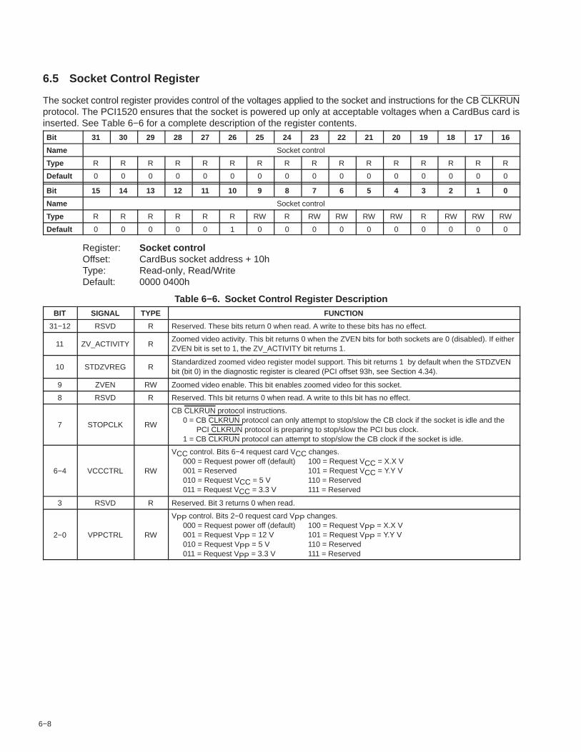
6−8
6.5 Socket Control Register
The socket control register provides control of the voltages applied to the socket and instructions for the CB CLKRUNprotocol. The PCI1520 ensures that the socket is powered up only at acceptable voltages when a CardBus card isinserted. See Table 6−6 for a complete description of the register contents.
Bit 31 30 29 28 27 26 25 24 23 22 21 20 19 18 17 16
Name Socket control
Type R R R R R R R R R R R R R R R R
Default 0 0 0 0 0 0 0 0 0 0 0 0 0 0 0 0
Bit 15 14 13 12 11 10 9 8 7 6 5 4 3 2 1 0
Name Socket control
Type R R R R R R RW R RW RW RW RW R RW RW RW
Default 0 0 0 0 0 1 0 0 0 0 0 0 0 0 0 0
Register: Socket controlOffset: CardBus socket address + 10hType: Read-only, Read/WriteDefault: 0000 0400h
Table 6−6. Socket Control Register DescriptionBIT SIGNAL TYPE FUNCTION
31−12 RSVD R Reserved. These bits return 0 when read. A write to these bits has no effect.
11 ZV_ACTIVITY RZoomed video activity. This bit returns 0 when the ZVEN bits for both sockets are 0 (disabled). If eitherZVEN bit is set to 1, the ZV_ACTIVITY bit returns 1.
10 STDZVREG RStandardized zoomed video register model support. This bit returns 1 by default when the STDZVENbit (bit 0) in the diagnostic register is cleared (PCI offset 93h, see Section 4.34).
9 ZVEN RW Zoomed video enable. This bit enables zoomed video for this socket.
8 RSVD R Reserved. ThIs bit returns 0 when read. A write to thIs bit has no effect.
7 STOPCLK RW
CB CLKRUN protocol instructions.0 = CB CLKRUN protocol can only attempt to stop/slow the CB clock if the socket is idle and the
PCI CLKRUN protocol is preparing to stop/slow the PCI bus clock.1 = CB CLKRUN protocol can attempt to stop/slow the CB clock if the socket is idle.
6−4 VCCCTRL RW
VCC control. Bits 6−4 request card VCC changes.000 = Request power off (default) 100 = Request VCC = X.X V001 = Reserved 101 = Request VCC = Y.Y V010 = Request VCC = 5 V 110 = Reserved011 = Request VCC = 3.3 V 111 = Reserved
3 RSVD R Reserved. Bit 3 returns 0 when read.
2−0 VPPCTRL RW
VPP control. Bits 2−0 request card VPP changes.000 = Request power off (default) 100 = Request VPP = X.X V001 = Request VPP = 12 V 101 = Request VPP = Y.Y V010 = Request VPP = 5 V 110 = Reserved011 = Request VPP = 3.3 V 111 = Reserved

6−9
6.6 Socket Power-Management Register
This register provides power management control over the socket through a mechanism for slowing or stopping theclock on the card interface when the card is idle. See Table 6−7 for a complete description of the register contents.
Bit 31 30 29 28 27 26 25 24 23 22 21 20 19 18 17 16
Name Socket power-management
Type R R R R R R R R R R R R R R R RW
Default 0 0 0 0 0 0 0 0 0 0 0 0 0 0 0 0
Bit 15 14 13 12 11 10 9 8 7 6 5 4 3 2 1 0
Name Socket power-management
Type R R R R R R R R R R R R R R R RW
Default 0 0 0 0 0 0 0 0 0 0 0 0 0 0 0 0
Register: Socket power-managementType: Read-only, Read/WriteOffset: CardBus socket address + 20hDefault: 0000 0000h
Table 6−7. Socket Power-Management Register DescriptionBIT SIGNAL TYPE FUNCTION
31−26 RSVD R Reserved. Bits 31−26 return 0s when read.
25 SKTACCES R
Socket access status. This bit provides information on when a socket access has occurred. This bit iscleared by a read access.
0 = A PC card access has not occurred (default).1 = A PC card access has occurred.
24 SKTMODE RSocket mode status. This bit provides clock mode information.
0 = Clock is operating normally.1 = Clock frequency has changed.
23−17 RSVD R Reserved. Bits 23−17 return 0s when read.
16 CLKCTRLEN RWCardBus clock control enable. When bit 16 is set, bit 0 (CLKCTRL) is enabled.
0 = Clock control is disabled (default).1 = Clock control is enabled.
15−1 RSVD R Reserved. Bits 15−1 return 0s when read.
0 CLKCTRL RW
CardBus clock control. This bit determines whether the CB CLKRUN protocol stops or slows the CB clockduring idle states. Bit 16 (CLKCTRLEN) enables this bit.
0 = Allows CB CLKRUN protocol to stop the CB clock (default).1 = Allows CB CLKRUN protocol to slow the CB clock by a factor of 16.

6−10
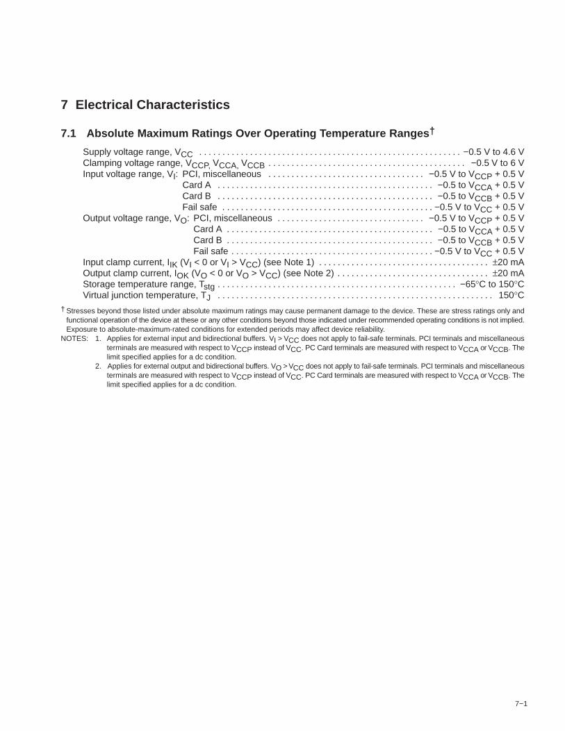
7−1
7 Electrical Characteristics
7.1 Absolute Maximum Ratings Over Operating Temperature Ranges †
Supply voltage range, VCC −0.5 V to 4.6 V. . . . . . . . . . . . . . . . . . . . . . . . . . . . . . . . . . . . . . . . . . . . . . . . . . . . . . . . . Clamping voltage range, VCCP, VCCA, VCCB −0.5 V to 6 V. . . . . . . . . . . . . . . . . . . . . . . . . . . . . . . . . . . . . . . . . . . Input voltage range, VI: PCI, miscellaneous −0.5 V to VCCP + 0.5 V. . . . . . . . . . . . . . . . . . . . . . . . . . . . . . . . . .
Card A −0.5 to VCCA + 0.5 V. . . . . . . . . . . . . . . . . . . . . . . . . . . . . . . . . . . . . . . . . . . . . . . Card B −0.5 to VCCB + 0.5 V. . . . . . . . . . . . . . . . . . . . . . . . . . . . . . . . . . . . . . . . . . . . . . . Fail safe −0.5 V to VCC + 0.5 V. . . . . . . . . . . . . . . . . . . . . . . . . . . . . . . . . . . . . . . . . . . . . .
Output voltage range, VO: PCI, miscellaneous −0.5 V to VCCP + 0.5 V. . . . . . . . . . . . . . . . . . . . . . . . . . . . . . . . Card A −0.5 to VCCA + 0.5 V. . . . . . . . . . . . . . . . . . . . . . . . . . . . . . . . . . . . . . . . . . . . . Card B −0.5 to VCCB + 0.5 V. . . . . . . . . . . . . . . . . . . . . . . . . . . . . . . . . . . . . . . . . . . . . Fail safe −0.5 V to VCC + 0.5 V. . . . . . . . . . . . . . . . . . . . . . . . . . . . . . . . . . . . . . . . . . . .
Input clamp current, IIK (VI < 0 or VI > VCC) (see Note 1) ±20 mA. . . . . . . . . . . . . . . . . . . . . . . . . . . . . . . . . . . . . Output clamp current, IOK (VO < 0 or VO > VCC) (see Note 2) ±20 mA. . . . . . . . . . . . . . . . . . . . . . . . . . . . . . . . . Storage temperature range, Tstg −65°C to 150°C. . . . . . . . . . . . . . . . . . . . . . . . . . . . . . . . . . . . . . . . . . . . . . . . . . . . Virtual junction temperature, TJ 150°C. . . . . . . . . . . . . . . . . . . . . . . . . . . . . . . . . . . . . . . . . . . . . . . . . . . . . . . . . . . .
† Stresses beyond those listed under absolute maximum ratings may cause permanent damage to the device. These are stress ratings only andfunctional operation of the device at these or any other conditions beyond those indicated under recommended operating conditions is not implied.Exposure to absolute-maximum-rated conditions for extended periods may affect device reliability.
NOTES: 1. Applies for external input and bidirectional buffers. VI > VCC does not apply to fail-safe terminals. PCI terminals and miscellaneousterminals are measured with respect to VCCP instead of VCC. PC Card terminals are measured with respect to VCCA or VCCB. Thelimit specified applies for a dc condition.
2. Applies for external output and bidirectional buffers. VO > VCC does not apply to fail-safe terminals. PCI terminals and miscellaneousterminals are measured with respect to VCCP instead of VCC. PC Card terminals are measured with respect to VCCA or VCCB. Thelimit specified applies for a dc condition.

7−2
7.2 Recommended Operating Conditions (see Note 3)
OPERATION MIN NOM MAX UNIT
VCC Core voltage Commercial 3.3 V 3 3.3 3.6 V
VCCPPCI and miscellaneous I/O clamp Commercial
3.3 V 3 3.3 3.6VVCCP
PCI and miscellaneous I/O clampvoltage
Commercial5 V 4.75 5 5.25
V
VCCA PC Card I/O clamp voltage Commercial3.3 V 3 3.3 3.6
VVCCAVCCB
PC Card I/O clamp voltage Commercial5 V 4.75 5 5.25
V
PCI3.3 V 0.5 VCCP VCCP
PCI5 V 2 VCCP
VIH† High-level input voltagePC Card
3.3 V 0.475 VCC(A/B) VCC(A/B) VVIH† High-level input voltagePC Card
5 V 2.4 VCC(A/B)
V
Miscellaneous‡ 2 VCC
PCI3.3 V 0 0.3 VCCP
PCI5 V 0 0.8
VIL† Low-level input voltagePC Card
3.3 V 0 0.325 VCC(A/B) VVIL† Low-level input voltagePC Card
5 V 0 0.8
V
Miscellaneous‡ 0 0.8
PCI 0 VCCP
VI Input voltage PC Card 0 VCC(A/B) VVI Input voltage
Miscellaneous‡ 0 VCC
V
PCI 0 VCC
VO§ Output voltage PC Card 0 VCC VVO§ Output voltage
Miscellaneous‡ 0 VCC
V
tt Input transition time (tr and tf)PCI and PC Card 1 4
nstt Input transition time (tr and tf) Miscellaneous‡ 0 6ns
TAOperating ambient temperature PCI1520 0 25 70
°CTAOperating ambient temperaturerange PCI1520I −40 25 85
°C
TJ¶ Virtual junction temperature 0 25 115 °C† Applies to external inputs and bidirectional buffers without hysteresis‡ Miscellaneous terminals are 15, 56, 68, 75, 83, 124, 137, 144, 158, and 177 for the PDV packaged device and C11, C15, G18, H05, J15, L18,
P07, P09, U08, and U11 for the GHK packaged device (SUSPEND, GRST, CDx, and VSx terminals).§ Applies to external output buffers¶ These junction temperatures reflect simulation conditions. The customer is responsible for verifying junction temperature.NOTE 3: Unused terminals (input or I/O) must be held high or low to prevent them from floating.

7−3
7.3 Electrical Characteristics Over Recommended Operating Conditions (unlessotherwise noted)
PARAMETER TERMINALS OPERATION TEST CONDITIONS MIN MAX UNIT
PCI3.3 V IOH = −0.5 mA 0.9 VCC
VPCI5 V IOH = −2 mA 2.4
V
SPKROUT3.3 V IOH = −0.5 mA 0.9 VCC
VOH High-level output voltageSPKROUT
5 V IOH = −1 mA 2.4VOH High-level output voltage
PC Card3.3 V IOH = −0.15 mA 0.9 VCC
PC Card5 V IOH = −0.15 mA 2.4 V
Miscellaneous IOH = −4 mA VCC−0.6
V
Miscellaneous IOH = −4 mA VCC−0.6
PCI3.3 V IOL = 1.5 mA 0.1 VCC
PCI5 V IOL = 6 mA 0.55
PC Card3.3 V IOL = 0.7 mA 0.1 VCC
VOL Low-level output voltagePC Card
5 V IOL = 0.7 mA 0.55 VVOL Low-level output voltage
Miscellaneous IOL = 4 mA 0.5
V
SPKROUT3.3 V IOL = 1 mA 0.1 VCC
SPKROUT5 V IOL = 1 mA 0.55
IOZLHigh-impedance, low-level output Output terminals
3.6 V VI = VCC −1AIOZL
High-impedance, low-level outputcurrent
Output terminals5.25 V VI = VCC −1
µA
IOZHHigh-impedance, high-level output Output terminals
3.6 V VI = VCC† 10AIOZH
High-impedance, high-level outputcurrent
Output terminals5.25 V VI = VCC† 25
µA
Input terminals VI = GND −1
IIL Low-level input current I/O terminals VI = GND −10 µAIIL Low-level input current
Pullup terminals VI = GND −330
µA
Input terminals3.6 V VI = VCC‡ 10
IIH High-level input current
Input terminals5.25 V VI = VCC‡ 20
µAIIH High-level input current
I/O terminals3.6 V VI = VCC‡ 10
µA
I/O terminals5.25 V VI = VCC‡ 25
† For PCI and miscellaneous terminals, VI = VCCP. For PC Card terminals, VI = VCC(A/B).‡ For I/O terminals, input leakage (IIL and IIH) includes IOZ leakage of the disabled output.
7.4 PCI Clock/Reset Timing Requirements Over Recommended Ranges of SupplyVoltage and Operating Free-Air Temperature
PARAMETERALTERNATE
SYMBOL TEST CONDITIONS MIN MAX UNIT
tc Cycle time, PCLK tcyc 30 ns
tw(H) Pulse duration (width), PCLK high thigh 11 ns
tw(L) Pulse duration (width), PCLK low tlow 11 ns
tr, tf Slew rate, PCLK ∆v/∆t 1 4 V/ns
tw Pulse duration (width), PRST trst 1 ms
tsu Setup time, PCLK active at end of PRST trst-clk 100 s

7−4
7.5 PCI Timing Requirements Over Recommended Ranges of Supply Voltage andOperating Free-Air Temperature
This data manual uses the following conventions to describe time ( t ) intervals. The format is tA, where subscript Aindicates the type of dynamic parameter being represented. One of the following is used: tpd = propagation delay time,td (ten, tdis) = delay time, tsu = setup time, and th = hold time.
PARAMETERALTERNATE
SYMBOL TEST CONDITIONS MIN MAX UNIT
tpd Propagation delay time, See Note 4
PCLK-to-shared signalvalid delay time
tvalCL = 50 pF,
11
nstpd Propagation delay time, See Note 4PCLK-to-shared signalinvalid delay time
tinv
CL = 50 pF, See Note 4
2ns
ten Enable time, high impedance-to-active delay time from PCLK ton 2 ns
tdis Disable time, active-to-high impedance delay time from PCLK toff 28 ns
tsu Setup time before PCLK valid tsu 7 ns
th Hold time after PCLK high th 0 ns
NOTE 4: PCI shared signals are AD31−AD0, C/BE3−C/BE0, FRAME, TRDY, IRDY, STOP, IDSEL, DEVSEL, and PAR.

8−1
8 Mechanical Information
The PCI1520 is packaged in either a 209-ball GHK/ZHK BGA or a 208-pin PDV package. The following show themechanical dimensions for the GHK, ZHK, and PDV packages.
GHK (S-PBGA-N209) PLASTIC BALL GRID ARRAY
19
14,40 TYP
1716
1314
151112
98 10
VU
W
R
NP
LM
K
T
756
34
H
FG
E
CD
1
AB
2
J
18
Seating Plane
4145273−2/B 12/98
SQ16,1015,90
0,95
0,450,35
0,550,45
0,120,08
0,85 1,40 MAX
0,10
0,80
0,80
M0,08
NOTES: A. All linear dimensions are in millimeters.B. This drawing is subject to change without notice.C. MicroStar BGA configuration.
MicroStar BGA is a trademark of Texas Instruments.

PACKAGE OPTION ADDENDUM
www.ti.com 26-May-2021
Addendum-Page 1
PACKAGING INFORMATION
Orderable Device Status(1)
Package Type PackageDrawing
Pins PackageQty
Eco Plan(2)
Lead finish/Ball material
(6)
MSL Peak Temp(3)
Op Temp (°C) Device Marking(4/5)
Samples
PCI1520IZWT ACTIVE NFBGA ZWT 209 90 RoHS & Green SNAGCU Level-3-260C-168 HR PCI1520IZWT
PCI1520PDV ACTIVE LQFP PDV 208 36 RoHS & Green NIPDAU Level-1-260C-UNLIM 0 to 70 PCI1520PDV
PCI1520PDVG4 ACTIVE LQFP PDV 208 36 RoHS & Green NIPDAU Level-1-260C-UNLIM 0 to 70 PCI1520PDV
PCI1520ZWT ACTIVE NFBGA ZWT 209 90 RoHS & Green SNAGCU Level-3-260C-168 HR PCI1520ZWT
(1) The marketing status values are defined as follows:ACTIVE: Product device recommended for new designs.LIFEBUY: TI has announced that the device will be discontinued, and a lifetime-buy period is in effect.NRND: Not recommended for new designs. Device is in production to support existing customers, but TI does not recommend using this part in a new design.PREVIEW: Device has been announced but is not in production. Samples may or may not be available.OBSOLETE: TI has discontinued the production of the device.
(2) RoHS: TI defines "RoHS" to mean semiconductor products that are compliant with the current EU RoHS requirements for all 10 RoHS substances, including the requirement that RoHS substancedo not exceed 0.1% by weight in homogeneous materials. Where designed to be soldered at high temperatures, "RoHS" products are suitable for use in specified lead-free processes. TI mayreference these types of products as "Pb-Free".RoHS Exempt: TI defines "RoHS Exempt" to mean products that contain lead but are compliant with EU RoHS pursuant to a specific EU RoHS exemption.Green: TI defines "Green" to mean the content of Chlorine (Cl) and Bromine (Br) based flame retardants meet JS709B low halogen requirements of <=1000ppm threshold. Antimony trioxide basedflame retardants must also meet the <=1000ppm threshold requirement.
(3) MSL, Peak Temp. - The Moisture Sensitivity Level rating according to the JEDEC industry standard classifications, and peak solder temperature.
(4) There may be additional marking, which relates to the logo, the lot trace code information, or the environmental category on the device.
(5) Multiple Device Markings will be inside parentheses. Only one Device Marking contained in parentheses and separated by a "~" will appear on a device. If a line is indented then it is a continuationof the previous line and the two combined represent the entire Device Marking for that device.
(6) Lead finish/Ball material - Orderable Devices may have multiple material finish options. Finish options are separated by a vertical ruled line. Lead finish/Ball material values may wrap to twolines if the finish value exceeds the maximum column width.
Important Information and Disclaimer:The information provided on this page represents TI's knowledge and belief as of the date that it is provided. TI bases its knowledge and belief on informationprovided by third parties, and makes no representation or warranty as to the accuracy of such information. Efforts are underway to better integrate information from third parties. TI has taken and

PACKAGE OPTION ADDENDUM
www.ti.com 26-May-2021
Addendum-Page 2
continues to take reasonable steps to provide representative and accurate information but may not have conducted destructive testing or chemical analysis on incoming materials and chemicals.TI and TI suppliers consider certain information to be proprietary, and thus CAS numbers and other limited information may not be available for release.
In no event shall TI's liability arising out of such information exceed the total purchase price of the TI part(s) at issue in this document sold by TI to Customer on an annual basis.
OTHER QUALIFIED VERSIONS OF PCI1520 :
• Enhanced Product : PCI1520-EP
NOTE: Qualified Version Definitions:
• Enhanced Product - Supports Defense, Aerospace and Medical Applications

TRAY
Chamfer on Tray corner indicates Pin 1 orientation of packed units.
*All dimensions are nominal
Device PackageName
PackageType
Pins SPQ Unit arraymatrix
Maxtemperature
(°C)
L (mm) W(mm)
K0(µm)
P1(mm)
CL(mm)
CW(mm)
PCI1520IZWT ZWT NFBGA 209 90 6 X 15 150 315 135.9 7620 20 17.5 15.45
PCI1520PDV PDV LQFP 208 36 4 x 9 150 315 135.9 7620 32.2 28.7 19.65
PCI1520PDVG4 PDV LQFP 208 36 4 x 9 150 315 135.9 7620 32.2 28.7 19.65
PCI1520ZWT ZWT NFBGA 209 90 6 X 15 150 315 135.9 7620 20 17.5 15.45
PACKAGE MATERIALS INFORMATION
www.ti.com 5-Jan-2022
Pack Materials-Page 1

IMPORTANT NOTICE AND DISCLAIMERTI PROVIDES TECHNICAL AND RELIABILITY DATA (INCLUDING DATA SHEETS), DESIGN RESOURCES (INCLUDING REFERENCE DESIGNS), APPLICATION OR OTHER DESIGN ADVICE, WEB TOOLS, SAFETY INFORMATION, AND OTHER RESOURCES “AS IS” AND WITH ALL FAULTS, AND DISCLAIMS ALL WARRANTIES, EXPRESS AND IMPLIED, INCLUDING WITHOUT LIMITATION ANY IMPLIED WARRANTIES OF MERCHANTABILITY, FITNESS FOR A PARTICULAR PURPOSE OR NON-INFRINGEMENT OF THIRD PARTY INTELLECTUAL PROPERTY RIGHTS.These resources are intended for skilled developers designing with TI products. You are solely responsible for (1) selecting the appropriate TI products for your application, (2) designing, validating and testing your application, and (3) ensuring your application meets applicable standards, and any other safety, security, regulatory or other requirements.These resources are subject to change without notice. TI grants you permission to use these resources only for development of an application that uses the TI products described in the resource. Other reproduction and display of these resources is prohibited. No license is granted to any other TI intellectual property right or to any third party intellectual property right. TI disclaims responsibility for, and you will fully indemnify TI and its representatives against, any claims, damages, costs, losses, and liabilities arising out of your use of these resources.TI’s products are provided subject to TI’s Terms of Sale or other applicable terms available either on ti.com or provided in conjunction with such TI products. TI’s provision of these resources does not expand or otherwise alter TI’s applicable warranties or warranty disclaimers for TI products.TI objects to and rejects any additional or different terms you may have proposed. IMPORTANT NOTICE
Mailing Address: Texas Instruments, Post Office Box 655303, Dallas, Texas 75265Copyright © 2022, Texas Instruments Incorporated