pci multi-channel i/o controller - freebsdlofi/envy24.pdf · pci multi-channel i/o controller...
TRANSCRIPT

PCI Multi-Channel I/O Controller
ICE1712
Preliminary
PCI Multi-ChannelI/O Controller
January 2000
IC Ensemble, Inc.3970 Freedom CircleSanta Clara, CA 95054-1204

PCI Multi-Channel I/O Controller
ICE1712
Preliminary
How to contact IC Ensemble, Inc.:
Tel: 1(408)9861200 ext.110 for Sales/Mktg/PRext.111 for Apps/Technical questions Fax: 1(408)9861490http://www.icensemble.com
Ordering Information• ICE1712 - 128PQFP
© 1998-2000 IC Ensemble, Inc. All Rights Reserved.
IC ENSEMBLE PRODUCTS ARE NOT AUTHORIZED FOR, AND SHOULD NOT BE USED WITHIN, LIFE SUPPORTSYSTEMS OR NUCLEAR FACILTY APPLICATIONS WITHOUT THE SPECIFIC WRITTEN CONSENT OF IC ENSEMBLE, Inc.Life support systems are those intended to support or sustain life, and show failure to perform when used as directed can reasonablyexpect to result in personal injury or death. Nuclear facilities are those involved in the production, handling, use, storage, disposal, orany other activity involving fissionable materials or their waste products.
IC Ensemble believes the information contained herein to be correct at the time of the publication. IC Ensemble reserves the right tomake changes at any time, without prior notice, to improve and supply the best possible product and is not responsible and does notassume any liability for misapplication or use outside the limits specified in this document.
IC Ensemble provides no warranty for the use of our products and assumes no liability for errors contained in this document.
IC Ensemble, the ICE logo are trademark of IC Ensemble, Inc. Other trademarks referenced in this document are owned by theirrespective companies.
Printed in the U.S.A.

Rev. 2.2, 1/03/00 i
PCI Multi-Channel I/O Controller
ICE1712
Preliminary
Table of Contents
Ordering Information . . . . . . . . . . . . . . . . . . . . . . . . . . . . . . . . . . . . . . . . . . . . . . . . . . . . . . . . . . ii
Table of Contents . . . . . . . . . . . . . . . . . . . . . . . . . . . . . . . . . . . . . . . . . . . . . . . . . . . . . . . . . . . . . . . . i
List of Figures . . . . . . . . . . . . . . . . . . . . . . . . . . . . . . . . . . . . . . . . . . . . . . . . . . . . . . . . . . . . . . . . . . . v
List of Tables. . . . . . . . . . . . . . . . . . . . . . . . . . . . . . . . . . . . . . . . . . . . . . . . . . . . . . . . . . . . . . . . . . . vi
Section 1: Introduction. . . . . . . . . . . . . . . . . . . . . . . . . . . . . . . . . . . . . . . . . . . . . . . . . . . . . . . . . . . . 7
1.1 Features. . . . . . . . . . . . . . . . . . . . . . . . . . . . . . . . . . . . . . . . . . . . . . . . . . . . . . . . . . . . . . . . . . . 8
1.2 Applications . . . . . . . . . . . . . . . . . . . . . . . . . . . . . . . . . . . . . . . . . . . . . . . . . . . . . . . . . . . . . . . 8
Section 2: Pins. . . . . . . . . . . . . . . . . . . . . . . . . . . . . . . . . . . . . . . . . . . . . . . . . . . . . . . . . . . . . . . . . 2-1
2.1 Pinout Diagram . . . . . . . . . . . . . . . . . . . . . . . . . . . . . . . . . . . . . . . . . . . . . . . . . . . . . . . . . . . 2-2
2.2 Pin Descriptions . . . . . . . . . . . . . . . . . . . . . . . . . . . . . . . . . . . . . . . . . . . . . . . . . . . . . . . . . . 2-3
2.3 Pin Lists . . . . . . . . . . . . . . . . . . . . . . . . . . . . . . . . . . . . . . . . . . . . . . . . . . . . . . . . . . . . . . . . 2-6
Section 3: PCI Interface and Configuration. . . . . . . . . . . . . . . . . . . . . . . . . . . . . . . . . . . . . . . . . 3-1PCI00: Vendor Identification Register. . . . . . . . . . . . . . . . . . . . . . . . . . . . . . . . . . . . . . . . . . . . . 3-2PCI02: Device Identification Register . . . . . . . . . . . . . . . . . . . . . . . . . . . . . . . . . . . . . . . . . . . . . 3-2PCI04: PCI Command Register . . . . . . . . . . . . . . . . . . . . . . . . . . . . . . . . . . . . . . . . . . . . . . . . . . 3-2PCI06: PCI Status Register. . . . . . . . . . . . . . . . . . . . . . . . . . . . . . . . . . . . . . . . . . . . . . . . . . . . . . 3-3PCI08: Revision ID Register. . . . . . . . . . . . . . . . . . . . . . . . . . . . . . . . . . . . . . . . . . . . . . . . . . . . . 3-3PCI0A: Class Code Register. . . . . . . . . . . . . . . . . . . . . . . . . . . . . . . . . . . . . . . . . . . . . . . . . . . . . 3-3PCI0C: Cache Size Register. . . . . . . . . . . . . . . . . . . . . . . . . . . . . . . . . . . . . . . . . . . . . . . . . . . . . 3-4PCI0D: Latency Timer Register . . . . . . . . . . . . . . . . . . . . . . . . . . . . . . . . . . . . . . . . . . . . . . . . . . 3-4PCI0E: Header Type Register. . . . . . . . . . . . . . . . . . . . . . . . . . . . . . . . . . . . . . . . . . . . . . . . . . . . 3-4PCI0F: BIST Register. . . . . . . . . . . . . . . . . . . . . . . . . . . . . . . . . . . . . . . . . . . . . . . . . . . . . . . . . . 3-4

ii Rev. 2.2, 1/03/00
PCI Multi-Channel I/O Controller
ICE1712
Preliminary
PCI10: Envy24 I/O Base . . . . . . . . . . . . . . . . . . . . . . . . . . . . . . . . . . . . . . . . . . . . . . . . . . . . . . . . 3-4PCI14: DDMA I/O Base . . . . . . . . . . . . . . . . . . . . . . . . . . . . . . . . . . . . . . . . . . . . . . . . . . . . . . . . 3-5PCI18: DMA Path Registers I/O Base . . . . . . . . . . . . . . . . . . . . . . . . . . . . . . . . . . . . . . . . . . . . . 3-5PCI1C: Multi-Track I/O Base . . . . . . . . . . . . . . . . . . . . . . . . . . . . . . . . . . . . . . . . . . . . . . . . . . . . 3-5PCI2C: Sub-Vendor ID . . . . . . . . . . . . . . . . . . . . . . . . . . . . . . . . . . . . . . . . . . . . . . . . . . . . . . . . . 3-5PCI34: Capability Pointer. . . . . . . . . . . . . . . . . . . . . . . . . . . . . . . . . . . . . . . . . . . . . . . . . . . . . . . 3-6PCI34: Interrupt Pin and Line. . . . . . . . . . . . . . . . . . . . . . . . . . . . . . . . . . . . . . . . . . . . . . . . . . . . 3-6PCI3E: Latency and Grant . . . . . . . . . . . . . . . . . . . . . . . . . . . . . . . . . . . . . . . . . . . . . . . . . . . . . . 3-6PCI40: Legacy Audio Control. . . . . . . . . . . . . . . . . . . . . . . . . . . . . . . . . . . . . . . . . . . . . . . . . . . . 3-7PCI42: Legacy Configuration Control . . . . . . . . . . . . . . . . . . . . . . . . . . . . . . . . . . . . . . . . . . . . . 3-8PCI60: System Configuration Register . . . . . . . . . . . . . . . . . . . . . . . . . . . . . . . . . . . . . . . . . . . . . 3-9PCI61: AC-Link Configuration Register. . . . . . . . . . . . . . . . . . . . . . . . . . . . . . . . . . . . . . . . . . . . 3-9PCI62: I2S Converters Features Register. . . . . . . . . . . . . . . . . . . . . . . . . . . . . . . . . . . . . . . . . . 3-10PCI63: S/PDIF Configuration Register . . . . . . . . . . . . . . . . . . . . . . . . . . . . . . . . . . . . . . . . . . . 3-10PCI80: Capability ID. . . . . . . . . . . . . . . . . . . . . . . . . . . . . . . . . . . . . . . . . . . . . . . . . . . . . . . . . . 3-10PCI81: Next Item Pointer . . . . . . . . . . . . . . . . . . . . . . . . . . . . . . . . . . . . . . . . . . . . . . . . . . . . . . 3-11PCI82: Power Management Capabilities . . . . . . . . . . . . . . . . . . . . . . . . . . . . . . . . . . . . . . . . . . 3-11PCI84: Power Management Control and Status. . . . . . . . . . . . . . . . . . . . . . . . . . . . . . . . . . . . . 3-11PCI86: PMCSR_Base and Data. . . . . . . . . . . . . . . . . . . . . . . . . . . . . . . . . . . . . . . . . . . . . . . . . . 3-12
Section 4: Hardware Interfaces. . . . . . . . . . . . . . . . . . . . . . . . . . . . . . . . . . . . . . . . . . . . . . . . . . . 4-1
4.1 Controller Registers . . . . . . . . . . . . . . . . . . . . . . . . . . . . . . . . . . . . . . . . . . . . . . . . . . . . . . . 4-3
CCS00: Control/Status Register . . . . . . . . . . . . . . . . . . . . . . . . . . . . . . . . . . . . . . . . . . . . . . . . . . 4-3CCS01: Interrupt Mask Register. . . . . . . . . . . . . . . . . . . . . . . . . . . . . . . . . . . . . . . . . . . . . . . . . . 4-4CCS02: Interrupt Status Register . . . . . . . . . . . . . . . . . . . . . . . . . . . . . . . . . . . . . . . . . . . . . . . . . 4-4CCS03: Envy24 Index Register . . . . . . . . . . . . . . . . . . . . . . . . . . . . . . . . . . . . . . . . . . . . . . . . . . . 4-5CCS04: Envy24 Data Register . . . . . . . . . . . . . . . . . . . . . . . . . . . . . . . . . . . . . . . . . . . . . . . . . . . 4-5CCS05: NMI Status Register 1 . . . . . . . . . . . . . . . . . . . . . . . . . . . . . . . . . . . . . . . . . . . . . . . . . . . 4-5CCS06: NMI Data Register. . . . . . . . . . . . . . . . . . . . . . . . . . . . . . . . . . . . . . . . . . . . . . . . . . . . . . 4-6CCS07: NMI Index Register . . . . . . . . . . . . . . . . . . . . . . . . . . . . . . . . . . . . . . . . . . . . . . . . . . . . . 4-6CCS08: Consumer AC’97 Index Register . . . . . . . . . . . . . . . . . . . . . . . . . . . . . . . . . . . . . . . . . . . 4-6CCS09: Consumer AC’97 Command and Status Register . . . . . . . . . . . . . . . . . . . . . . . . . . . . . . 4-7CCS0A: Consumer AC’97 Data Port Register . . . . . . . . . . . . . . . . . . . . . . . . . . . . . . . . . . . . . . . 4-7CCS0C: Primary MIDI UART Data Register . . . . . . . . . . . . . . . . . . . . . . . . . . . . . . . . . . . . . . . . 4-7CCS0D: Primary MIDI UART Command/Status Register . . . . . . . . . . . . . . . . . . . . . . . . . . . . . . 4-8CCS0E: NMI Status Register 2. . . . . . . . . . . . . . . . . . . . . . . . . . . . . . . . . . . . . . . . . . . . . . . . . . . . 4-8CCS0F: Game Port Register. . . . . . . . . . . . . . . . . . . . . . . . . . . . . . . . . . . . . . . . . . . . . . . . . . . . . 4-8CCS10: I2C Port Device Address Register . . . . . . . . . . . . . . . . . . . . . . . . . . . . . . . . . . . . . . . . . . 4-9CCS11: I2C Port Byte Address Register . . . . . . . . . . . . . . . . . . . . . . . . . . . . . . . . . . . . . . . . . . . . 4-9CCS12: I2C Port Read/Write Data Register . . . . . . . . . . . . . . . . . . . . . . . . . . . . . . . . . . . . . . . . . 4-9CCS13: I2C Port Control and Status Register. . . . . . . . . . . . . . . . . . . . . . . . . . . . . . . . . . . . . . . 4-10CCS14: Consumer Record DMA Current/Base Address Register . . . . . . . . . . . . . . . . . . . . . . . 4-10CCS18: Consumer Record DMA Current/Base Count Register. . . . . . . . . . . . . . . . . . . . . . . . . 4-10CCS1B: PCI Configuration SERR# Shadow Register. . . . . . . . . . . . . . . . . . . . . . . . . . . . . . . . . 4-11CCS1C: Secondary MIDI UART Data Register . . . . . . . . . . . . . . . . . . . . . . . . . . . . . . . . . . . . . 4-11

Rev. 2.2, 1/03/00 iii
PCI Multi-Channel I/O Controller
ICE1712
Preliminary
CCS1D: Secondary MIDI UART Command/Status Register . . . . . . . . . . . . . . . . . . . . . . . . . . . 4-11CCS1E: Timer Register. . . . . . . . . . . . . . . . . . . . . . . . . . . . . . . . . . . . . . . . . . . . . . . . . . . . . . . . 4-11
4.1.1 Controller Indexed Registers . . . . . . . . . . . . . . . . . . . . . . . . . . . . . . . . . . . . . . . . . . . . 4-12
CCI00: Playback Terminal Count Register (High Byte) . . . . . . . . . . . . . . . . . . . . . . . . . . . . . . 4-12CCI01: Playback Terminal Count Register (Low Byte) . . . . . . . . . . . . . . . . . . . . . . . . . . . . . . . 4-12CCI02: Playback Control Register. . . . . . . . . . . . . . . . . . . . . . . . . . . . . . . . . . . . . . . . . . . . . . . 4-12CCI03: Playback Left Volume/Pan Register . . . . . . . . . . . . . . . . . . . . . . . . . . . . . . . . . . . . . . . . 4-13CCI04: Playback Right Volume/Pan Register . . . . . . . . . . . . . . . . . . . . . . . . . . . . . . . . . . . . . . 4-13CCI05: Soft Volume/Mute Control Register. . . . . . . . . . . . . . . . . . . . . . . . . . . . . . . . . . . . . . . . 4-13CCI06: Playback Sampling Rate Register (Low Byte) . . . . . . . . . . . . . . . . . . . . . . . . . . . . . . . . 4-14CCI07: Playback Sampling Rate Register (Middle Byte). . . . . . . . . . . . . . . . . . . . . . . . . . . . . . 4-14CCI08: Playback Sampling Rate Register (High Byte) . . . . . . . . . . . . . . . . . . . . . . . . . . . . . . . 4-14CCI10: Record Current/Base Terminal Count Register (High Byte). . . . . . . . . . . . . . . . . . . . . 4-14CCI11: Record Current/Base Terminal Count Register (Low Byte) . . . . . . . . . . . . . . . . . . . . . 4-15CCI12: Record Control Register. . . . . . . . . . . . . . . . . . . . . . . . . . . . . . . . . . . . . . . . . . . . . . . . . 4-15CCI20: GPIO Data Register. . . . . . . . . . . . . . . . . . . . . . . . . . . . . . . . . . . . . . . . . . . . . . . . . . . . 4-15CCI21: GPIO Write Mask Register . . . . . . . . . . . . . . . . . . . . . . . . . . . . . . . . . . . . . . . . . . . . . . 4-16CCI22: GPIO Direction Control Register . . . . . . . . . . . . . . . . . . . . . . . . . . . . . . . . . . . . . . . . . 4-16CCI30: Consumer Section Power Down Register . . . . . . . . . . . . . . . . . . . . . . . . . . . . . . . . . . . 4-16CCI31: Multi-Track Section Power Down Register. . . . . . . . . . . . . . . . . . . . . . . . . . . . . . . . . . 4-17
4.2 DDMA Registers . . . . . . . . . . . . . . . . . . . . . . . . . . . . . . . . . . . . . . . . . . . . . . . . . . . . . . . . 4-18
4.3 DMA Path Descriptions . . . . . . . . . . . . . . . . . . . . . . . . . . . . . . . . . . . . . . . . . . . . . . . . . . . 4-19
4.4 Consumer Section DMA Channel Registers . . . . . . . . . . . . . . . . . . . . . . . . . . . . . . . . . . . 4-20
DS0: DirectSound DMA Interrupt Mask Register:. . . . . . . . . . . . . . . . . . . . . . . . . . . . . . . . . . . 4-20DS2: DirectSound DMA Interrupt Status Register: . . . . . . . . . . . . . . . . . . . . . . . . . . . . . . . . . . 4-20DS4: Channel Data Register:. . . . . . . . . . . . . . . . . . . . . . . . . . . . . . . . . . . . . . . . . . . . . . . . . . . 4-20DS8: Channel Index Register . . . . . . . . . . . . . . . . . . . . . . . . . . . . . . . . . . . . . . . . . . . . . . . . . . . 4-21Channel Control and Status Register at Index 4h (DS8 = x4h). . . . . . . . . . . . . . . . . . . . . . . . . . 4-22Consumer mode Sampling Rate Register at Index 5h (DS8 = x5h). . . . . . . . . . . . . . . . . . . . . . . 4-22Consumer mode Left/Right Volume Register at Index 06h (DS8 = x6h). . . . . . . . . . . . . . . . . . . 4-23
4.5 Professional Multi-Track Control Registers . . . . . . . . . . . . . . . . . . . . . . . . . . . . . . . . . . . . 4-24
4.5.1 Multi-Track Mode Control Registers . . . . . . . . . . . . . . . . . . . . . . . . . . . . . . . . . . . . . . 4-24
MT00: Professional section DMA Interrupt Mask and Status Register: . . . . . . . . . . . . . . . . . . 4-24MT01: Professional section Sampling Rate Select Register: . . . . . . . . . . . . . . . . . . . . . . . . . . . 4-25MT02: Professional codec I²S Data Format Register:. . . . . . . . . . . . . . . . . . . . . . . . . . . . . . . . 4-26MT04: Index Register for AC’97 Codecs on Professional section. . . . . . . . . . . . . . . . . . . . . . . 4-26MT05: Command and Status Register for AC’97 Codecs on Professional Section. . . . . . . . . . . 4-29MT06: Data Port Register for AC’97 codecs on Professional section. . . . . . . . . . . . . . . . . . . . 4-29
4.5.2 Multi-Track Playback Registers . . . . . . . . . . . . . . . . . . . . . . . . . . . . . . . . . . . . . . . . . . 4-30
MT10: Professional Section Playback DMA Current/Base Address Register . . . . . . . . . . . . . . 4-30MT14: Professional Section Playback DMA Current/Base Count Register. . . . . . . . . . . . . . . . 4-31MT16: Professional Section Playback Current/Base Terminal Count Register. . . . . . . . . . . . . 4-31

iv Rev. 2.2, 1/03/00
PCI Multi-Channel I/O Controller
ICE1712
Preliminary
MT18: Professional Section Playback and Record Control Register. . . . . . . . . . . . . . . . . . . . . 4-31
4.5.3 Multi-Track Record Registers . . . . . . . . . . . . . . . . . . . . . . . . . . . . . . . . . . . . . . . . . . . 4-32
MT20: Professional Section Record DMA Current/Base Address Register . . . . . . . . . . . . . . . . 4-32MT24: Professional Section Record DMA Current/Base Count Register. . . . . . . . . . . . . . . . . . 4-32MT26: Professional Section Record Current/Base Terminal Count Register . . . . . . . . . . . . . . . 4-32MT28: Professional Section Record Control Register . . . . . . . . . . . . . . . . . . . . . . . . . . . . . . . . 4-32
4.5.4 Professional Section Digital Loopback. . . . . . . . . . . . . . . . . . . . . . . . . . . . . . . . . . . . . 4-33
MT30: Routing Control Register for Data to PSDOUT[0:3] . . . . . . . . . . . . . . . . . . . . . . . . . . . 4-34MT32: Routing Control Register for SPDOUT . . . . . . . . . . . . . . . . . . . . . . . . . . . . . . . . . . . . . . 4-35MT34: Captured (Recorded) data Routing Selection Register. . . . . . . . . . . . . . . . . . . . . . . . . . . 4-36
4.5.5 Multi-Track Digital Monitoring . . . . . . . . . . . . . . . . . . . . . . . . . . . . . . . . . . . . . . . . . . 4-39
MT38: Left/Right Volume Control Data Register. . . . . . . . . . . . . . . . . . . . . . . . . . . . . . . . . . . . . 4-39MT3A: Volume Control Stream Index Register:. . . . . . . . . . . . . . . . . . . . . . . . . . . . . . . . . . . . . . 4-40MT3B: Volume Control Rate Register . . . . . . . . . . . . . . . . . . . . . . . . . . . . . . . . . . . . . . . . . . . . . 4-40MT3C: Digital Mixer Monitor Routing Control Register . . . . . . . . . . . . . . . . . . . . . . . . . . . . . . 4-41MT3E: Peak Meter Index Register. . . . . . . . . . . . . . . . . . . . . . . . . . . . . . . . . . . . . . . . . . . . . . . . 4-42MT3F: Peak Meter Data Register . . . . . . . . . . . . . . . . . . . . . . . . . . . . . . . . . . . . . . . . . . . . . . . . 4-42
Section 5: Electrical Characteristics. . . . . . . . . . . . . . . . . . . . . . . . . . . . . . . . . . . . . . . . . . . . . . . 5-15.1 Maximum Ratings. . . . . . . . . . . . . . . . . . . . . . . . . . . . . . . . . . . . . . . . . . . . . . . . . . . . . . . . . 5-1
5.2 Electrical Specifications . . . . . . . . . . . . . . . . . . . . . . . . . . . . . . . . . . . . . . . . . . . . . . . . . . . . 5-1
5.3 AC Timing Characteristics . . . . . . . . . . . . . . . . . . . . . . . . . . . . . . . . . . . . . . . . . . . . . . . . . . 5-2
Section 6: Mechanical Data . . . . . . . . . . . . . . . . . . . . . . . . . . . . . . . . . . . . . . . . . . . . . . . . . . . . . . 6-16.1 Thermal Specifications . . . . . . . . . . . . . . . . . . . . . . . . . . . . . . . . . . . . . . . . . . . . . . . . . . . . . 6-1
6.2 Package Dimensions . . . . . . . . . . . . . . . . . . . . . . . . . . . . . . . . . . . . . . . . . . . . . . . . . . . . . . . 6-2
Section 7: Appendix . . . . . . . . . . . . . . . . . . . . . . . . . . . . . . . . . . . . . . . . . . . . . . . . . . . . . . . . . . . . 7-17.1 Appendix A. . . . . . . . . . . . . . . . . . . . . . . . . . . . . . . . . . . . . . . . . . . . . . . . . . . . . . . . . . . . . . 7-1

Rev. 2.2, 1/03/00 v
PCI Multi-Channel I/O Controller
ICE1712
Preliminary
List of Figures
Figure 2-1. 128-pin PQFP Package . . . . . . . . . . . . . . . . . . . . . . . . . . . . . . . . . . . . . . . . . . . . . . . . . . . . . . 2-2Figure 4-1. Functional Block Diagram. . . . . . . . . . . . . . . . . . . . . . . . . . . . . . . . . . . . . . . . . . . . . . . . . . . . 4-2Figure 4-2. I²S Format Timing Diagram . . . . . . . . . . . . . . . . . . . . . . . . . . . . . . . . . . . . . . . . . . . . . . . . . 4-26Figure 4-3. Crystals to Master Clocks clock generation tree . . . . . . . . . . . . . . . . . . . . . . . . . . . . . . . . . . 4-27Figure 4-4. Master Clocks to Bit Clocks, L/R Clocks and Sync generation . . . . . . . . . . . . . . . . . . . . . . 4-28Figure 4-5. Multi-track DMA transfer diagram . . . . . . . . . . . . . . . . . . . . . . . . . . . . . . . . . . . . . . . . . . . . 4-30Figure 4-6. Data stream routing capabilities . . . . . . . . . . . . . . . . . . . . . . . . . . . . . . . . . . . . . . . . . . . . . . 4-33Figure 4-7. Digital Mixer Functional Diagram . . . . . . . . . . . . . . . . . . . . . . . . . . . . . . . . . . . . . . . . . . . . 4-41Figure 5-1. Cold Reset Timing . . . . . . . . . . . . . . . . . . . . . . . . . . . . . . . . . . . . . . . . . . . . . . . . . . . . . . . . . . 5-2Figure 5-2. Warm Reset Timing. . . . . . . . . . . . . . . . . . . . . . . . . . . . . . . . . . . . . . . . . . . . . . . . . . . . . . . . . 5-3Figure 5-3. Master Clock Delay . . . . . . . . . . . . . . . . . . . . . . . . . . . . . . . . . . . . . . . . . . . . . . . . . . . . . . . . . 5-3Figure 5-4. xBCLK to xxSYNC Timing . . . . . . . . . . . . . . . . . . . . . . . . . . . . . . . . . . . . . . . . . . . . . . . . . . 5-4Figure 5-5. Setup and Hold Time . . . . . . . . . . . . . . . . . . . . . . . . . . . . . . . . . . . . . . . . . . . . . . . . . . . . . . . . 5-5Figure 5-6. Rise Time and Fall Time . . . . . . . . . . . . . . . . . . . . . . . . . . . . . . . . . . . . . . . . . . . . . . . . . . . . . 5-6Figure 5-7. AC-link Power Mode Timing. . . . . . . . . . . . . . . . . . . . . . . . . . . . . . . . . . . . . . . . . . . . . . . . . . 5-6

vi Rev. 2.2, 1/03/00
PCI Multi-Channel I/O Controller
ICE1712
Preliminary
List of Tables
Table 2-1. Pin Descriptions . . . . . . . . . . . . . . . . . . . . . . . . . . . . . . . . . . . . . . . . . . . . . . . . . . . . . . . . . . . 2-3Table 2-2. Alphabetical Pin Listing . . . . . . . . . . . . . . . . . . . . . . . . . . . . . . . . . . . . . . . . . . . . . . . . . . . . . 2-6Table 2-3. Numerical Pin Listing . . . . . . . . . . . . . . . . . . . . . . . . . . . . . . . . . . . . . . . . . . . . . . . . . . . . . . . 2-8Table 3-1. PCI Host Interface Register Map . . . . . . . . . . . . . . . . . . . . . . . . . . . . . . . . . . . . . . . . . . . . . . . 3-1Table 4-1. CCSxx Controller Register Map . . . . . . . . . . . . . . . . . . . . . . . . . . . . . . . . . . . . . . . . . . . . . . . 4-3Table 4-2. DMA Channels and respective functionality . . . . . . . . . . . . . . . . . . . . . . . . . . . . . . . . . . . . 4-19Table 4-3. DSx Consumer DMA Channel Register Map . . . . . . . . . . . . . . . . . . . . . . . . . . . . . . . . . . . . 4-20Table 4-4. DS8 Register, Low Nibble Index Description Applicable to Channel-0 through D . . . . . . . 4-21Table 4-5. Channel parameter controls . . . . . . . . . . . . . . . . . . . . . . . . . . . . . . . . . . . . . . . . . . . . . . . . . . 4-23Table 4-6. MTxx Controller Register Map . . . . . . . . . . . . . . . . . . . . . . . . . . . . . . . . . . . . . . . . . . . . . . . 4-24Table 5-2. DC Characteristics . . . . . . . . . . . . . . . . . . . . . . . . . . . . . . . . . . . . . . . . . . . . . . . . . . . . . . . . . . 5-1Table 5-1. Maximum Ratings . . . . . . . . . . . . . . . . . . . . . . . . . . . . . . . . . . . . . . . . . . . . . . . . . . . . . . . . . . 5-1Table 5-3. Power Consumption . . . . . . . . . . . . . . . . . . . . . . . . . . . . . . . . . . . . . . . . . . . . . . . . . . . . . . . . . 5-2Table 5-4. Cold Reset . . . . . . . . . . . . . . . . . . . . . . . . . . . . . . . . . . . . . . . . . . . . . . . . . . . . . . . . . . . . . . . . 5-2Table 5-5. Warm Reset . . . . . . . . . . . . . . . . . . . . . . . . . . . . . . . . . . . . . . . . . . . . . . . . . . . . . . . . . . . . . . . 5-3Table 5-6. Slave Mode Master clock delay . . . . . . . . . . . . . . . . . . . . . . . . . . . . . . . . . . . . . . . . . . . . . . . 5-3Table 5-7. xBCLK / xxSYNC Timing. . . . . . . . . . . . . . . . . . . . . . . . . . . . . . . . . . . . . . . . . . . . . . . . . . . . 5-4Table 5-8. Setup and Hold . . . . . . . . . . . . . . . . . . . . . . . . . . . . . . . . . . . . . . . . . . . . . . . . . . . . . . . . . . . . . 5-5Table 5-9. Rise and Fall Time . . . . . . . . . . . . . . . . . . . . . . . . . . . . . . . . . . . . . . . . . . . . . . . . . . . . . . . . . . 5-5Table 5-10. AC-link Low Power Mode. . . . . . . . . . . . . . . . . . . . . . . . . . . . . . . . . . . . . . . . . . . . . . . . . . . . 5-6Table 6-1. Mechanical Dimensions (millimeters, unless otherwise stated) . . . . . . . . . . . . . . . . . . . . . . . 6-2Table 7-1. AC-link Interface Parameters and Ratios (when pin 50 floating/pulled up) . . . . . . . . . . . . . . 7-1Table 7-2. I²S Interface Parameters and Ratios (when pin 50 pulled down). . . . . . . . . . . . . . . . . . . . . . . 7-1Table 7-3. S/PDIF Output I²S Interface Parameters and Ratios . . . . . . . . . . . . . . . . . . . . . . . . . . . . . . . . 7-2Table 7-4. S/PDIF Input I²S Interface Parameters and Ratios. . . . . . . . . . . . . . . . . . . . . . . . . . . . . . . . . . 7-2

Introduction Rev. 2.2, 1/05/99 1 - 7
PCI Multi-Channel I/O Controller
ICE1712
Preliminary
Section 1: Introduction
The Envy24TM is a versatile PCI multi-channel I/O controller. It allows up to 12x2 simultaneous input andoutput channels with the data source or destination being either analog or digital. Some of the typicalapplications for this part are computer based multi-track audio, multi-channel audio, PC-based dataacquisition, waveform generation and computer telephony integration. The Envy24 can be combined withprofessional grade I²S converters, S/PDIF transmitters/receivers or AC-link codecs, such as the ICE1232TM.The controller integrates a very high resolution digital mixer allowing up to 20 channels of mixing. This isaimed specifically for monitoring final outputs, making master copies and for budget conscious studios thatmay lack an individual out-board mixer.
The Envy24 supplies a master I²C interface providing connection to an E²PROM to store and retrieve PCISubsystem and Subsystem vendor IDs, specific board configurations and custom features identification. Thisinterface is available for controlling other devices as well.
For target markets where legacy audio is still important, the SoundBlaster Pro compatible hardware ensureshardware compatibility under DOS for DDMA (Distributed DMA) and non-DDMA systems. The device alsoincludes a Microsoft Win9x architecture based DirectSound hardware accelerator that interfaces to AC’97 viaAC-link. The separate path allows concurrent operation with the 24-bit professional multi-track audio section.
The Envy24 is a “Digital-Ready” audio device allowing acceleration in cooperation with the host andredirecting audio streams to other endpoints.
The Envy24 integrates two independent MPU-401 MIDI UARTs. This features allows hooking up multipleexternal MIDI devices and dedicating the two paths for different purposes.
Additionally, a conventional standard Joystick port and timer is integrated. Only R and C components arenecessary to complete the circuit. Also an 8-bit GPIO brings flexibility for multi-purpose use.
The Envy24 is a power miser device due to its aggressive power management scheme and hard-wired designarchitecture. The device is ACPI compliant making it suitable for platforms designed for “OnNow”.
Depending on the sampling rates that need to be supported by the target solution, one or two crystals aresufficient to operate the whole system. Alternatively, a PLL Clock synthesizer chip can be used to generate thenecessary frequencies. The clock chip can be controlled by the GPIO pins for programmability.
For more detail on the part, please refer to the system block diagram Figure 4-1 in Section 4.

1 - 8 Rev. 2.2, 1/05/99 Introduction
PCI Multi-Channel I/O Controller
ICE1712
Preliminary
1.1 Features
• PCI 2.1 I/F with bus mastering and burst modes• 24-bit resolution audio format support• Sampling rates up to 96kHz• 8x2 I/O on AC-link or I²S, up to 4x2 converters• Simultaneous I²S for S/PDIF I/O up to 96kHz• 20 channels, 36-bit wide digital mixer• Monitor and master copy functions• Peak meters on all 20 professional multi-track streams• Concurrent 16 streams DirectSoundTM accelerator• Sample Rate Converter for DirectSound applications• Two MPU-401 MIDI UART ports• ACPI and PCI PMI support• I²C subset I/F for E²PROM (configuration and ID storage) and peripherals control• HW SoundBlaster® Pro legacy • FM synthesis for DOS® legacy• 64-voices SW Wavetable General MIDI Synthesizer for Windows95• DirectInputTM compatible Joystick port• 8-bit GPIO port• Windows® 95/98, NT4.0 drivers• 24.576, 16.9344 or 22.5792 MHz crystal operation• 3.3V operating supply (5V tolerant I/O)• 128-pin PQFP (14mm x 20mm body)
1.2 Applications
• PC-based multi-track audio• Discrete multi-channel audio• High-end PCI audio• “Pro-sumer” audio• General purpose multi-channel I/O• Computer telephony• PC-based data acquisition• PC-based waveform generation• PC-based instrumentation• PC-based control and automation

Pins Rev. 2.2, 4/26/99 2 - 1
PCI Multi-Channel I/O Controller
ICE1712
Preliminary
Section 2: Pins
The following section includes the pinout diagram of the chip that is housed in a standard 128-PQFP. Also,three lists of pin assignments are provided for your convenience. They are logically sorted by functionality anddescription, alphabetically and numerically sorted in ascending order. These list are provided to assisthardware development, test, debugging and quality assurance. The mechanical data about the part can be foundin Section 6.

2 - 2 Rev. 2.2, 4/26/99 Pins
PCI Multi-Channel I/O Controller
ICE1712
Preliminary
2.1 Pinout Diagram
Figure 2-1. 128-pin PQFP Package
VDD 1AD24 2
CBE3# 3IDSEL 4AD23 5AD22 6VSS 7
AD21 8AD20 9AD19 10AD18 11AD17 12VDD 13VSS 14
AD16 15CBE2# 16
FRAME# 17IRDY# 18
TRDY# 19VSS 20
DEVSEL# 21STOP# 22SERR# 23
PAR 24CBE1# 25
VSS 26VDD 27
AD15 28AD14 29AD13 30
39 40 41 42 43 44 45 46 47 48 49 50 51 52 53 54 55 56 57 58102 JSD2101 JSD3100 VSS99 JSD498 JSD597 JSD696 JSD795 TX194 RX193 VDD92 CMCLK91 CSDOUT90 CBCLK89 CSDIN88 CSYNC87 VSS86 CRST#85 PMCLK84 PSDOUT[3]83 PSDOUT[2]82 PSDOUT[1]81 VDD80 VSS79 PSDOUT[0]78 PBCLK77 PSDIN[3]76 PSDIN[2]75 PSDIN[1]74 VSS73 PSDIN[0]
128V
SS
127A
D25
126A
D26
125A
D27
124A
D28
123A
D29
122V
DD
121A
D30
120A
D31
119R
EQ
#118
GN
T#
117P
CIC
LK116
VS
S115
VD
D114
RS
T#
113IN
TA
#112
SP
MC
LKO
UT
111S
PM
CLK
IN110
SP
SC
LK109
SP
SY
NC
ICE
1712
AD12 31AD11 32VSS 33
AD10 34AD9 35AD8 36
CBE0# 37VDD 38
72 PSYNC71 SCLK70 SDA69 TESTEN#68 NC67 VDD_X166 XOUT165 XIN1
59 60 61 62 63 64
108V
SS
107S
PD
IN106
SP
DO
UT
105P
RS
T#
104JS
D0
103JS
D1
VS
SA
D7
AD
6A
D5
AD
4A
D3
VD
DV
SS
AD
2A
D1
AD
0G
PIO
0G
PIO
1G
PIO
2G
PIO
3V
DD
VS
SG
PIO
4G
PIO
5G
PIO
6/TX2
GP
IO7/R
X2
VS
S_X
2X
IN2
XO
UT2
VD
D_X
2V
SS
_X1

Pins Rev. 2.2, 4/26/99 2 - 3
PCI Multi-Channel I/O Controller
ICE1712
Preliminary
2.2 Pin Descriptions
The following table provides a brief description of each pin of the ICE1712. Pins with dual usage may be listedtwice for consistency. The following abbreviations are used to identify the pin types.I - Input SignalO - Output SignalB - Bidirectional SignalOD - Open DrainA - Analog SignalPU - Pull-up. 50kΩ nominal
Table 2-1. Pin Descriptions
Symbol Type Description
PCI BUS INTERFACE
AD[31:0] B Multiplexed PCI Address/Data Bus.
CBE#[3:0]B Bus command/Byte Lane Enable. These signals are bus commands
during the address phase and byte lane enable during the data phase.These signals are output during a bus master cycle.
PCICLK I PCI Bus Clock.
DEVSEL#B Device Select. The ICE1712 drives this signal active when it decodes its
address as the current target of the current acces.
FRAME#B PCI Cycle Frame. When asserted by the bus mster, this signal indicates
the beginning of a bus transaction.During the final data phase of a bustransaction it is deasserted.
GNT# I When active it indicates bus master is granted to ICE1712.
IDSELI Initialization Device Select. This is the chip select during the PCI
configuration register accesses
INTA# OD PCI Interrupt Request.
IRDY# B Initiator Ready.
PAR B Parity Signal.
REQ# O Bus master control request
RST#I System Reset. All ICE1712 registers and state machines are at default
when this signal is asserted.
SERR# OD PCI System Error
STOP# B Target disconnect signal.
TRDY# B Target Ready.
I²C PORT
SDA B Serial bidirectional dat.
SCLK O Serial bit shift clock
GAME PORT

2 - 4 Rev. 2.2, 4/26/99 Pins
PCI Multi-Channel I/O Controller
ICE1712
Preliminary
JSD[7:4] I Joystick Fire buttons
JSD[3:0] A Joystick CoordinateS inputs
PRIMARY MPU-401 UART
TX1 O, PU Primary MPU-401 Transmit data
RX1 I, PU Primary MPU-401 Receive data
SECONDARY MPU-401 UART
TX2/GPIO6 O Secondary MPU-401 Transmit data
RX2/GPIO7 I Secondary MPU-401 Receive data
CONSUMER AC-LINK INTERFACE
CSYNC O 48kHz fixed rate sync pulse
CBCLK I 12.288MHz Serial Bit Clock
CSDIN I Incoming Serial Data Stream
CSDOUT O Outbound Serial Data Stream
CMCLKO Master Clock for AC’97 codec. Outputs XIN1 crystal frequency, typically
24.576 MHz .
CRST# O Consumer Codec master reset
PROFESSIONAL MULTI-TRACK AC-LINK / I ²S INTERFACE
PSYNCO AC’97: 48kHz fixed rate sync pulse for up to 4 codecs, or
8 I²S type converters: Left/Right Clock
PBCLK I/O Serial Bit Clock. It can be master or slave configured
PSDIN[3:0] I 4 separate incoming stereo stream pairs
PSDOUT[3:0] O 4 separate outbound stereo stream pairs
PMCLK O Master Clock for AC’97 codecs or I²S converters
PRST# O Cold reset for Professional Multi-track I²S/AC-link I/F
CLOCKS
XOUT1 A Clock Out 1
XIN1 A 24.576MHz (512*48kHz). Runs all fixed clock blocks.
XOUT2 A Clock Out 2
XIN2A 16.9344MHz (384*44.1kHz) or 22.5792MHz (512*44.1kHz) or external
PLL output
S/PDIF (SONY/PHILIPS DIGITAL INTERFACE)
SPMCLKIN I S/PDIF Master Clock Input
SPMCLKOUT O S/PDIF Master Clock Output
SPSCLK O S/PDIF Serial Bit Clock
Table 2-1. Pin Descriptions (continued)
Symbol Type Description
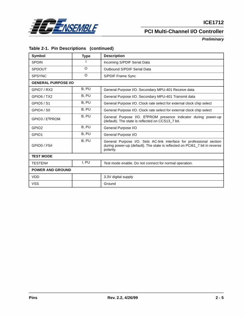
Pins Rev. 2.2, 4/26/99 2 - 5
PCI Multi-Channel I/O Controller
ICE1712
Preliminary
SPDIN I Incoming S/PDIF Serial Data
SPDOUT O Outbound S/PDIF Serial Data
SPSYNC O S/PDIF Frame Sync
GENERAL PURPOSE I/O
GPIO7 / RX2 B, PU General Purpose I/O. Secondary MPU-401 Receive data
GPIO6 / TX2 B, PU General Purpose I/O. Secondary MPU-401 Transmit data
GPIO5 / S1 B, PU General Purpose I/O. Clock rate select for external clock chip select
GPIO4 / S0 B, PU General Purpose I/O. Clock rate select for external clock chip select
GPIO3 / E²PROMB, PU General Purpose I/O. E²PROM presence indicator during power-up
(default). The state is reflected on CCS13_7 bit.
GPIO2 B, PU General Purpose I/O
GPIO1 B, PU General Purpose I/O
GPIO0 / I²S#B, PU General Purpose I/O. Sets AC-link interface for professional section
during power-up (default). The state is reflected on PCI61_7 bit in reversepolarity.
TEST MODE
TESTEN# I, PU Test mode enable. Do not connect for normal operation.
POWER AND GROUND
VDD 3.3V digital supply
VSS Ground
Table 2-1. Pin Descriptions (continued)
Symbol Type Description

2 - 6 Rev. 2.2, 4/26/99 Pins
PCI Multi-Channel I/O Controller
ICE1712
Preliminary
2.3 Pin Lists
Table 2-2 lists all the pins alphabetically. Table 2-3 lists all the pins in numerical order.
Table 2-2. Alphabetical Pin Listing
Symbol Pin(s)
AD[31:0] 2, 5-6, 8-12, 15, 28-32, 34-36, 40-44, 47-49, 120-121, 123-127,
CBCLK 90
CBE#[3:0] 3, 16, 25, 37
CMCLK 92
CRST# 86
CSDIN 89
CSDOUT 91
CSYNC 88
DEVSEL# 21
FRAME# 17
GNT# 118
GPIO[0]/I²S# 50
GPIO[1] 51
GPIO[2] 52
GPIO[3]/E²PROM 53
GPIO[4]/S0 56
GPIO[5]/S1 57
GPIO[6]/TX2 58
GPIO[7]/RX2 59
IDSEL 4
INTA# 113
IRDY# 19
JSD[7:0] 96-99, 101-104
PAR 24
PBCLK 78
PCICLK 117
PMCLK 85
PRST# 105
PSDIN[3:0] 73, 75-77
PSDOUT[3:0] 79, 82-84

Pins Rev. 2.2, 4/26/99 2 - 7
PCI Multi-Channel I/O Controller
ICE1712
Preliminary
PSYNC 72
REQ# 119
RST# 114
RX1 94
RX2/GPIO[7] 59
SCLK 71
SDA 70
SPDIN 107
SPDOUT 106
SERR# 23
SPMCLKIN 111
SPMCLKOUT 112
SPSCLK 110
SPSYNC 109
STOP# 22
TESTEN# 69
TRDY# 19
TX1 95
TX2/GPIO[6] 58
VDD 1, 13, 27, 38, 45, 54, 81, 115, 122
VDD_X1 67
VDD_X2 63
VSS 7, 14,20, 26, 33, 39, 46, 55, 74, 80, 87, 100, 108, 116, 128
VSS_X1 64
VSS_X2 60
XIN[2:1] 61, 65
XOUT[2:1] 62, 66
Table 2-2. Alphabetical Pin Listing (continued)
Symbol Pin(s)

2 - 8 Rev. 2.2, 4/26/99 Pins
PCI Multi-Channel I/O Controller
ICE1712
Preliminary
Table 2-3. Numerical Pin Listing
Pin # Symbol Pin # Symbol
1 VDD 65 XOUT1
2 AD24 66 VDD_X1
3 CBE3# 67 VDD
4 IDSEL 68 VSS
5 AD23 69 TESTEN#
6 AD22 70 SDA
7 VSS 71 SCLK
8 AD21 72 PSYNC
9 AD20 73 PSDIN[0]
10 AD19 74 VSS
11 AD18 75 PSDIN[1]
12 AD17 76 PSDIN[2]
13 VDD 77 PSDIN[3]
14 VSS 78 PBCLK
15 AD16 79 PSDOUT[0]
16 CBE2# 80 VSS
17 FRAME# 81 VDD
18 IRDY# 82 PSDOUT[1]
19 TRDY# 83 PSDOUT[2]
20 VSS 84 PSDOUT[3]
21 DEVSEL# 85 PMCLK
22 STOP# 86 CRST#
23 SERR# 87 VSS
24 PAR 88 CSYNC
25 CBE1# 89 CSDIN
26 VSS 90 CBCLK
27 VDD 91 CSDOUT
28 AD15 92 CMCLK
29 AD14 93 VDD
30 AD13 94 RX1
31 AD12 95 TX1
32 AD11 96 JSD7
33 VSS 97 JSD6

Pins Rev. 2.2, 4/26/99 2 - 9
PCI Multi-Channel I/O Controller
ICE1712
Preliminary
34 AD10 98 JSD5
35 AD9 99 JSD4
36 AD8 100 VSS
37 CBE0# 101 JSD3
38 VDD 102 JSD2
39 VSS 103 JSD1
40 AD7 104 JSD0
41 AD6 105 TX2
42 AD5 106 SPDOUT
43 AD4 107 SPDIN
44 AD3 108 VDD
45 VDD 109 SPSYNC
46 VSS 110 SPSCLK
47 AD2 111 SPMCLKIN
48 AD1 112 SPMCLKOUT
49 AD0 113 INTA#
50 GPIO[0] 114 RST#
51 GPIO[1] 115 VDD
52 GPIO[2] 116 VSS
53 GPIO[3] 117 PCICLK
54 VDD 118 GNT#
55 GPIO[4]/S0 119 REQ#
56 GPIO[5]/S1 120 AD31
57 GPIO[6]/TX2 121 AD30
58 GPIO[7]/RX2 122 VDD
59 VSS_X2 123 AD29
60 XIN2 124 AD28
61 XOUT2 125 AD27
62 VDD_X2 126 AD26
63 VSS_X1 127 AD25
64 XIN1 128 VSS
Table 2-3. Numerical Pin Listing (continued)
Pin # Symbol Pin # Symbol

2 - 10 Rev. 2.2, 4/26/99 Pins
PCI Multi-Channel I/O Controller
ICE1712
Preliminary

PCI Interface and Configuration Rev. 2.2, 1/03/00 3 - 1
PCI Multi-Channel I/O Controller
ICE1712
Preliminary
Section 3: PCI Interface and Configuration
Table 3-1. PCI Host Interface Register Map
Byte 3 Byte 2 Byte 1 Byte 0 Offset (Hex)
Device Identification Vendor Identification 00
PCI Device Status PCI Command 04
Class Code Reserved. Read as 0 Revision ID 08
BIST Header Type Latency Timer Reserved. Read as 0 0C
Controller I/O Base Address 10
DDMA I/O Base Address 14
DMA Path Registers I/O Base Address 18
Professional Multi-Track I/O Base Address 1C
Subsystem ID Subsystem Vendor ID 2C
Reserved. Read as 0 30
Capability Pointer 34
Reserved. Read as 0 38
Minimum Latency and Maximum Grant Interrupt Pin and Line 3C
Legacy Configuration Control Legacy Audio Control 40
Hardware Configuration Control 60
Power Management Capability Next Item Pointer Capability ID 80
PMCSR Support Extensions and Data Power Management Control and Status 84

3 - 2 Rev. 2.2, 1/03/00 PCI Interface and Configuration
PCI Multi-Channel I/O Controller
ICE1712
Preliminary
3.1 Envy24 PCI Configuration Registers
PCI00: Vendor Identification Register
Address Offset: 00 - 01h
Default Value: 1412h
PCI02: Device Identification Register
Address Offset: 02 - 03h
Default Value: 1712h
PCI04: PCI Command Register
Address Offset: 04 - 05h
Default Value: 0000h
Bit Attribute Description
15:0 RO Vendor Identification Number. This is the 16-bit value assigned to IC Ensemble, Inc.
Bit Attribute Description
15:0 RO Device Identification Number. 1712 reflects the part number.
Bit Attribute Description
15:10 R0b Reserved. Read as 0s.
9 R0b Fast Back-to-Back Enable. This bit is hardwired to 0 (Not Implemented).
8 R/WSERR# enable. 1= enable. 0=disable (default).When enabled, FM and MIDI I/O writes will be trapped and causes SERR# asserted. PCISTS register reports the status of the SERR# signal.This bit has a shadow defined in register bit CCS1B_0.
7 R0b A/D stepping enable. This bit is hardwired to 0 (Not Implemented).
6 R0b Parity error detect enable. Hardwired to 0 (Not Implemented).
5 R0b VGA palette snoop enable. Hardwired to 0 (Not Implemented).
4 R0b Memory write and invalidate enable. Hardwired to 0 (Not Implemented).
3 R0b Special Cycle Enable (SCE). Hardwired to 0 (Not Implemented).
2 R/W Bus master enable. 1=enable. 0=disable (default).
1 R0b Memory Access. Hardwired to 0 (Not Implemented).
0 R/W I/O Space accesses enable. 1=enable. 0=disable (default).

PCI Interface and Configuration Rev. 2.2, 1/03/00 3 - 3
PCI Multi-Channel I/O Controller
ICE1712
Preliminary
PCI06: PCI Status Register
Address Offset: 06 - 07h
Default Value: 0210h
PCI08: Revision ID Register
Address Offset: 08h - 09h
Default Value: 000Xh
PCI0A: Class Code Register
Address Offset: 0Ah - 0Bh
Default Value: 0401h
Bit Attribute Description
15 R/W/C PAR status. Parity error detected (even when parity not enabled).
14 R/W/C SERR# status. This bit is set to 1 when SERR# is asserted (even when it is not enabled) and cleared by writing 1 to it.
13 R/W/C Master abort status. This bit is set to 1 when master aborts and cleared by writing "1" to it.
12 R/W/C Received target abort status. This bit is set to 1 when target abort is received and cleared by writing a 1 to it.
11 R0b Signaled target abort status. This bit is set when target abort generated and cleared by writing a 1 to it. Hardwired to 0 (never abort).
10:9 R10b DEVSEL# timing status. Envy24 always asserts DEVSEL# with medium timing.
8 R0b PERR# response. Read as 0 (Not Implemented).
7 R0b Fast back to back. Read as 0 (Not implemented).
6 R0b User Define Function (UDF). Read as 0 (Not implemented).
5 R0b Reserved. Read as 0. 33MHz only.
4 R1b Hardwired to 1 to indicate the support for PCI power management capability.
3:0 R0000b Reserved. Read as 0s.
Bit Attribute Description
15:0 R00h -
7:0 RO Revision ID
Bit Attribute Description
15:8 RO Base Class. Reflects Multimedia
7:0 RO Sub class. Reflects Audio.

3 - 4 Rev. 2.2, 1/03/00 PCI Interface and Configuration
PCI Multi-Channel I/O Controller
ICE1712
Preliminary
PCI0C: Cache Size Register
Address Offset: 0Ch
Default Value: 00h
PCI0D: Latency Timer Register
Address Offset: 0Dh
Default Value: 00h
PCI0E: Header Type Register
Address Offset: 0Eh
Default Value: 00h
PCI0F: BIST Register
Address Offset: 0Fh
Default Value: 00h
PCI10: Envy24 I/O Base
Address Offset: 10h - 13h
Default Value: 00000001h
Bit Attribute Description
7:0 RO Read as 0. Not supported
Bit Attribute Description
7:3 R/W Latency timer
2:0 RO Read as 0
Bit Attribute Description
7:0 RO Read as 0
Bit Attribute Description
7:0 RO Read as 0. Not supported
Bit Attribute Description
31:5 RW Controller I/O Base Address for CCSxx registers described in section 4.1
4:1 R0h Hardwired to 0 to have 32 bytes I/O space. This includes UARTs and game port.
0 R1b Hardwired to 1 to indicate registers map to I/O space

PCI Interface and Configuration Rev. 2.2, 1/03/00 3 - 5
PCI Multi-Channel I/O Controller
ICE1712
Preliminary
PCI14: DDMA I/O Base
Address Offset: 14h -17h
Default Value: 00000001h
PCI18: DMA Path Registers I/O Base
Address Offset: 18h - 1Bh
Default Value: 00000001h
PCI1C: Multi-Track I/O Base
Address Offset: 1Ch - 1Fh
Default Value: 00000001h
PCI2C: Sub-Vendor ID
Address Offset: 2Ch - 2Fh
Default Value: 17121412h
Bit Attribute Description
31:4 R/W DDMA Slave Channel Base Address for DDMAx registers described in section 4.2
3:1 R000b Hardwired to 0 to have 16 bytes I/O space
0 R1b Hardwired to 1 to indicate registers map to I/O space
Bit Attribute Description
31:4 R/W DMA path registers I/O Base Address for DSx registers described in section 4.4
3:1 R000b Hardwired to 0 to specify requirement of 16 bytes I/O space
0 R1b Hardwired to 1 to indicate registers map to I/O space
Bit Attribute Description
31:6 R/W Multi-Track I/O Base Address for MTxx registers described in section 4.5
5:1 R0 Hardwired to 0 to have 64 bytes I/O space
0 R1b Hardwired to 1 to indicate registers map to I/O space
Bit Attribute Description
31:0 RO Sub-vendor ID: Read it from external E²PROM after reset if it exists, otherwise, same as vendor ID. It can also be written by disabling write protection bit defined in PCI42_7.

3 - 6 Rev. 2.2, 1/03/00 PCI Interface and Configuration
PCI Multi-Channel I/O Controller
ICE1712
Preliminary
PCI34: Capability Pointer
Address Offset: 34h
Default Value: 80h
PCI34: Interrupt Pin and Line
Address Offset: 3Ch - 3Dh
Default Value: 01FFh
PCI3E: Latency and Grant
Address Offset: 3Eh - 3Fh
Default Value: 0000h
Bit Attribute Description
7:0 RO CP7-CP0: Capability data structure pointer for PCI power management. Hardwired to 80h.
Bit Attribute Description
15:8 RO 01h read from this register indicates the interrupt pin used is INTA# and cannot be modified.
7:0 R/W Interrupt line routing information set by POST during power-up initialization. Default FFh indicates no connection to the PIC yet.
Bit Attribute Description
15:8 RO Maximum latency
7:0 RO Minimum grant

PCI Interface and Configuration Rev. 2.2, 1/03/00 3 - 7
PCI Multi-Channel I/O Controller
ICE1712
Preliminary
PCI40: Legacy Audio Control
Address Offset: 40h - 41h
Default Value: 807Fh
Bit Attribute Description
15 R/W0: Legacy Audio Hardware enable.1: Legacy Audio Hardware disabled (default)
14:12 R000b -
11:10 R/W Reserved
9:8 R/W Reserved
7:6 R/W
SB DMA Channel Select:00 DMA 001 DMA 1 (default)10 Reserved11 DMA 3
5 R/WI/O Address Alias Control 1: select the 10-bit decode (default)0: select the 16-bit decode In either case, the AD(31:16) should be zero
4 R/W Reserved
3 R/W MPU-401 I/O enable
2 R/W Game Port enable (200h)
1 R/W FM I/O enable (AdLib 388h base)
0 R/W SB I/O enable

3 - 8 Rev. 2.2, 1/03/00 PCI Interface and Configuration
PCI Multi-Channel I/O Controller
ICE1712
Preliminary
PCI42: Legacy Configuration Control
Address Offset: 42h - 43h
Default Value: 0006h
Bit Attribute Description
15:8 R/W Interrupt vector to be snooped.
7 R/W0: SVID read only. (default)1: SVID read/write enable.
6 R/W0: snoop SB 22C/24Ch I/O write cycle to assert SERR#: disable (default)1: snoop SB 22C/24Ch I/O write cycle to assert SERR# : enable
5 R/W0: snoop PIC I/O R/W cycle to assert SERR#: disable (default)1: snoop PIC I/O R/W cycle to assert SERR#: enable
4 R/W0: snoop PCI bus interrupt acknowledge cycle: disable (default)1: snoop PCI bus interrupt acknowledge cycle: enable
3 R/W0: SB base 220h (default)1: SB base 240h
2:1 R/W
0: MPU-401 base 300h1: MPU-401 base 310h2: MPU-401 base 320h3: MPU-401 base 330h (default)
0 RW0: DDMA enable (default)1: Legacy DMA enable

PCI Interface and Configuration Rev. 2.2, 1/03/00 3 - 9
PCI Multi-Channel I/O Controller
ICE1712
Preliminary
PCI60: System Configuration Register
Address Offset: 60h
Default Value: 0Fh
The following four bytes (60h-63h) should be read from E2PROM by driver and then written to setup the codecconfiguration, unless otherwise noted.
PCI61: AC-Link Configuration Register
Address Offset: 61h
Default Value: 00h
Except for bit 7, the four bytes at 60h-63h should be read from E2PROM by driver and then written to setup thecodec configuration.
Bit Attribute Description
7:6 R/W
XIN2 Clock Source Configuration. Refer to register MT01 and Table 7-2 in the Appendix00: XIN2: 22.5792MHz crystal (44.1kHz*512)01: XIN2: 16.9344MHz crystal (44.1kHz*384)10: XIN2: from external clock synthesizer chip (e.g. MK1412) which needs to be controlled via S0, S1 pins. These shared GPIO4 and 5 pins become write only and the direction will not be controllable via CCI22.11: - Reserved
5 R/W0: one MPU-401 UART only1: two MPU-401 UARTs.
4 R/WConsumer AC'97 codec: 0: Consumer AC'97 does exist1: Consumer AC'97 does not exist
3:2 R/W
Must have at least one pair of professional multi-track ADC and DAC. 00: one stereo ADC connected 01: two stereo ADCs connected10: three stereo ADCs connected11: four stereo ADCs connected
1:0 R/W
Must have at least one pair of professional multi-track ADC and DAC. 00: one stereo DAC connected 01: two stereo DACs connected 10: three stereo DACs connected 11: four stereo DACs connected
Bit Attribute Description
7 R/WMulti-track converter type: 0: AC'97 1: I²S. Reflects power-up status of pin 50 during reset cycle in reverse polarity. Can be overwritten
6:2 R/W Reserved.
1 R/WIf bit 7 is 0:0: split mode: AC’97 codec SDATA_OUT split to different pin outputs1: packed mode: AC’97 codec SDATA_OUT packed in slots 3 to 10
3 - 10 Rev. 2.2, 1/03/00 PCI Interface and Configuration
PCI Multi-Channel I/O Controller
ICE1712
Preliminary
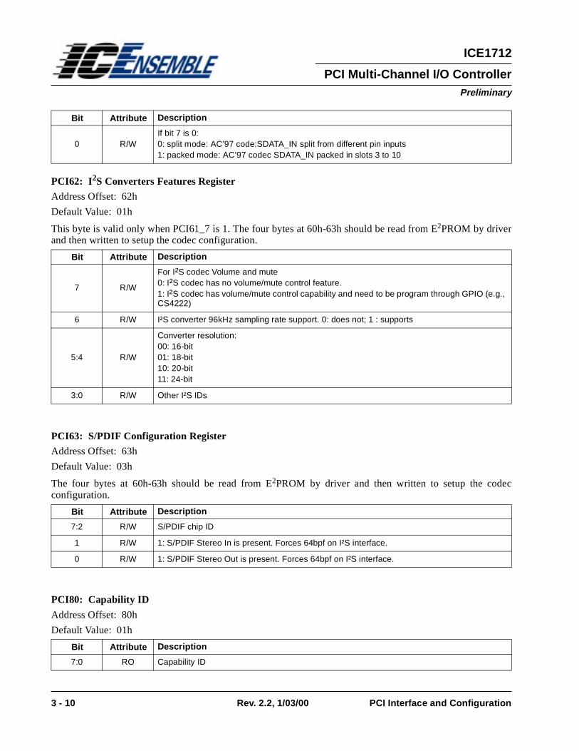
PCI62: I2S Converters Features Register
Address Offset: 62h
Default Value: 01h
This byte is valid only when PCI61_7 is 1. The four bytes at 60h-63h should be read from E2PROM by driverand then written to setup the codec configuration.
PCI63: S/PDIF Configuration Register
Address Offset: 63h
Default Value: 03h
The four bytes at 60h-63h should be read from E2PROM by driver and then written to setup the codecconfiguration.
PCI80: Capability ID
Address Offset: 80h
Default Value: 01h
0 R/WIf bit 7 is 0:0: split mode: AC’97 code:SDATA_IN split from different pin inputs 1: packed mode: AC’97 codec SDATA_IN packed in slots 3 to 10
Bit Attribute Description
7 R/W
For I²S codec Volume and mute0: I²S codec has no volume/mute control feature.1: I²S codec has volume/mute control capability and need to be program through GPIO (e.g., CS4222)
6 R/W I²S converter 96kHz sampling rate support. 0: does not; 1 : supports
5:4 R/W
Converter resolution:00: 16-bit01: 18-bit10: 20-bit11: 24-bit
3:0 R/W Other I²S IDs
Bit Attribute Description
7:2 R/W S/PDIF chip ID
1 R/W 1: S/PDIF Stereo In is present. Forces 64bpf on I²S interface.
0 R/W 1: S/PDIF Stereo Out is present. Forces 64bpf on I²S interface.
Bit Attribute Description
7:0 RO Capability ID
Bit Attribute Description

PCI Interface and Configuration Rev. 2.2, 1/03/00 3 - 11
PCI Multi-Channel I/O Controller
ICE1712
Preliminary
PCI81: Next Item PointerAddress Offset: 81hDefault Value: 00h
PCI82: Power Management Capabilities
Address Offset: 82h - 83h
Default Value: 0401h
PCI84: Power Management Control and Status
Address Offset: 84h - 85h
Default Value: 0000h
Bit Attribute Description
7:0 RO Hardwired to 0 to indicate the end of list
Bit Attribute Description
15:11 RO PME not supported. Hardwired to 0.
10 R1 D2 state support. Hardwire to 1.
9 R0 D1 state not support. Hardwired to 0.
8:6 R000 Reserved.
5 R0 DSI. Hardwired to 0.
4 R0 Aux. Power. Hardwired to 0
3 R0 PMC clock for generation of PME#. Hardwired to 0.
2:0 R001b Hardwired to 001 to indicate PPMI 1.0 compliance
Bit Attribute Description
15 R0b PME status. Read as 0.
14:13 R00b Data scale. Not supported.
12:9 R0h Data select: Not supported.
8 R0b PME assertion. Hardwired to 0
7:2 RO Hardwired to 000000
1:0 R/W
Power state. To determine the current state of power state.00 : D001 : D1 (not supported)10 : D211 : D3_hot

3 - 12 Rev. 2.2, 1/03/00 PCI Interface and Configuration
PCI Multi-Channel I/O Controller
ICE1712
Preliminary
PCI86: PMCSR_Base and Data
Address Offset: 86h - 87h
Default Value: 0000h
Bit Attribute Description
15:0 R0000h -

Hardware Interfaces Rev. 2.2, 1/03/00 4 - 1
PCI Multi-Channel I/O Controller
ICE1712
Preliminary
Section 4: Hardware Interfaces
In the previous section PCI host interface and configuration registers were discussed. In this section descriptionof the major blocks, their respective hardware interfaces and associated registers will be discussed. In mostcases the four I/O base addresses have a one to one correspondence with the major functional blocks.Therefore, the following sub-chapters will be organized based on the logical grouping of the registers on theoffsets of their respective I/O base addresses.
The first figure in this section, Figure 4-1, is a chip level block diagram with typical external interface usage. Itis a very good overview of the whole chip, but should not be regarded as the most detailed diagram. Asappropriate, the databook will resort to sub-block diagrams to further detail the functionality. These are themulti-track DMA transfer mechanism, data stream routing capabilities and the digital mixer block diagram.

4 - 2R
ev. 2.2, 1/03/00H
ardware Interfaces
PC
I Multi-C
hannel I/O C
ontroller
ICE
1712
Figure 4-1. Functional Block Diagram
10x24b ch.
Σ
I2S I/OFour I 2Sor AC-Link
Pairs
Four I 2Sor AC-Link
Pairs
S/PDIF I/O 4 ADC/Codec4 DAC/Codec AC’97 Codec
AC-Link I/F
16 ch. SRC and DSDigital Mixer
DirectSoundDMA
LegacyAudio
RecordDMA
12x24b ch.
2x20b ch.2x16b ch.
14 str. 8/16b packed path
DMA DMA
20 Ch., 36bDigital Mixer
MPU-401UART
MPU-401UART
I²C/E²PROMPORT
8-bitGPIO
JoystickPort
RX1 TX1 RX2 TX2 SD GPIO JSD
PCI 2.1 Bus Master BIU with Burst Mode
PCI BUS
10x24b ch.
.10x24b ch.
Σ
I2S I/OFour I 2Sor AC-Link
Pairs
Four I 2Sor AC-Link
Pairs
S/PDIF I/O 4 ADC/Codec4 DAC/Codec AC’97 Codec
AC-Link I/F
16 ch. SRC and DSDigital Mixer
DirectSoundDMA
Legacyand PCM
RecordDMA
12x24b ch. 2x20b ch.2x16b ch.
14 str. 8/16b packed path
DMA DMA
20 Ch., 36bDigital Mixer
MPU-401UART
MPU-401UART
I²C/E²PROMPORT
8-bitGPIO
JoystickPort
RX1 TX1 RX2 TX2 SD GPIO JSD
PCI 2.1 Bus Master BIU with Burst Mode
PCI BUS
10x24b ch.
.

Hardware Interfaces Rev. 2.2, 1/03/00 4 - 3
PCI Multi-Channel I/O Controller
ICE1712
Preliminary
4.1 Controller Registers
The following registers are offset from base address set by PCI10. The 32 bytes I/O space includes maincontrol/status registers, I2C interface, MPU-401 MIDI UARTs and game port control as well. Each CCSxxregister is physically located at the address determined by [PCI10]+xx and accessed directly. The registers canbe accessed as a byte, word or dword register.
Table 4-1. CCSxx Controller Register Map
CCS00: Control/Status Register
Address Offset: 00h
Default Value: 00h
Byte 3 Byte 2 Byte 1 Byte 0 Offset (Hex)
CCIxx Index Envy24 Status Interrupt Mask Envy24 Control/Stat. 00
NMI Index NMI Data NMI Status 1 CCIxx Data 04
Consumer AC ‘97 Data Port C. AC ‘97 Comm./Stat. Cons. AC ‘97 Index 08
Game Port NMI Status 2 MIDI 1 Comm./Status MIDI UART 1 Data 0C
I²C Port Control/Status I²C Port R/W Data I²C Port Byte Address I²C Port Dev. Address 10
Consumer Record DMA Current/Base Address 14
SERR# Shadow - Consumer Record DMA Count Address 18
Timer MIDI 2 Comm./Status MIDI UART 2 Data 1C
Bit Attribute Description
7 R/W Entire Chip soft reset
6 R/W Legacy mode only: 1: enable SERR# assertion for the DS DMA Channel-C interrupt 0: disable SERR# assertion for the DS DMA Channel-C interrupt (default)
5 RO
4 R/W Legacy mode only:1: set the DOS WT volume control coming from DS Channel-C/D index registers B.0: set the DOS FM volume control coming from SB mixer register space. (default) This bit is used in the legacy mode for the switching between FM and WT under DOS. For FM and WT under Windows, it is always coming from DS Channel-C/D index register B.
3 R/W 0: SERR# level (default) 1: SERR# edge (only one PCI clock width)
2 R0 -
1 R/W Legacy mode only:1: enable SERR# assertion for SB interrupt0: disable SERR# assertion for SB interrupt (default)
0 R/W Mode select: 0: SB mode 1: native mode

4 - 4 Rev. 2.2, 1/03/00 Hardware Interfaces
PCI Multi-Channel I/O Controller
ICE1712
Preliminary
CCS01: Interrupt Mask Register
Address Offset: 01h
Default Value: FEh
CCS02: Interrupt Status Register
Address Offset: 02h
Default Value: 00h.
These bits are sticky and only writing a 1 to that bit location will clear itself.
Bit Attribute Description
7 R/W Primary MIDI interrupt mask
6 R/W Timer mask
5 R/W Secondary MIDI interrupt mask.
4 R/W Professional Multi-track playback and record. This is the macro interrupt mask for both playback and record.
3 R/W FM/MIDI trapping interrupt mask
2 R/W Playback DS DMA channels mask (effective for all the playback DMA channels from 0 to D)
1 R/W Consumer record DMA channel interrupt mask
0 R/W Consumer/SB mode playback interrupt mask (DMA channel E and F)
Bit Attribute Description
7 R/W/C Primary MIDI receiver FIFO
6 R/W/C Timer
5 R/W/C Secondary MIDI receiver FIFO
4 RO Multi-track playback or record. This is the macro interrupt status for both playback and record. To clear individual status bit, write a 1 to the associated bit location defined in section 4.4.
3 R/W/C FM/MIDI trapping
2 RO Direct Sound. This is the macro interrupt status for DS Channels (0 through D). To clear individual status bit, Write a 1 to the associated bit location defined in the DS DMA channel register section.
1 R/W/C Native mode record (Record DMA)
0 R/W/C Native/SB playback

Hardware Interfaces Rev. 2.2, 1/03/00 4 - 5
PCI Multi-Channel I/O Controller
ICE1712
Preliminary
CCS03: Envy24 Index Register
Address Offset: 03h
Default Value: 00h
CCS04: Envy24 Data Register
Address Offset: 04h
Default Value: 00h.
CCS05: NMI Status Register 1
Address Offset: 05h
Default Value: 00h
Description: This register pertains to legacy audio hardware synthesis emulation in DOS. Reading from thisregister will clear itself and de-assert the SERR# signal. However, it will not clear the SERR# bit PCI06_14.To clear it, write 1 to that bit location instead. Refer to register CCS0E as well.
Bit Attribute Description
7:6 R00b -
5:0 R/W Index register. Write the CCIxx register’s xx index as described in section 4.1.1.
Bit Attribute Description
7:0 See 4.1.1 Data register. Content for CCIxx register.
Bit Attribute Description
7 RO 1: PCI I/O read/write cycle if bit PCI43_5 is set to 1.
6 RO 1: SB 22C/24C write if bit PCI 43_6 is set to 1.
5 R0b -
4 RO 1: SB interrupt (either SB DMA or SB F2 command) if bit [PCI10]_1 is set to 1.
3 RO 1: DS channel C DMA interrupt (for FM/WT data transfer DMA) if bit [PCI10]_6 is set to 1.
2 RO 1: MIDI 330h or [PCI_10]h+Ch write
1 R0 -
0 RO 1: FM data register write (389h/221h/229h/38bh/223h)

4 - 6 Rev. 2.2, 1/03/00 Hardware Interfaces
PCI Multi-Channel I/O Controller
ICE1712
Preliminary
CCS06: NMI Data Register
Address Offset: 06h
Default Value: 00h
Description: This register pertains to legacy audio hardware synthesis emulation in DOS.
CCS07: NMI Index Register
Address Offset: 07h
Default Value: 00h
Description: This register pertains to legacy audio hardware synthesis emulation in DOS.
CCS08: Consumer AC’97 Index Register
Address Offset: 08h
Default Value: 00h
Bit Attribute Description
7:0 RO Trapped data for TSR to be read (either FM 389h(221h,229h)/38bh(223h), MIDI 330h write, PIC I/O or SB 22C/24C write cycle (if enabled). Note that only write to FM data will assert SERR# but not write to FM index.
Bit Attribute Description
7:0 RO Trapped data for FM Index only.
Bit Attribute Description
7 R0b -
6:0 R/W AC’97 registers Index. Refer to the AC’97 specification for register descriptions.

Hardware Interfaces Rev. 2.2, 1/03/00 4 - 7
PCI Multi-Channel I/O Controller
ICE1712
Preliminary
CCS09: Consumer AC’97 Command and Status Register
Address Offset: 09h
Default Value: 00h
CCS0A: Consumer AC’97 Data Port Register
Address Offset: 0Ah - 0Bh
Default Value: 0000h
CCS0C: Primary MIDI UART Data Register
Address Offset: 0Ch
Default Value: 00h
Bit Attribute Description
7 R/W Cold reset W: 1 to cold reset the codec. 0: CRST# will be de-asserted.
6 R/W Warm reset W: 1 to warm reset the codec by asserting CSYNC. 0: CSYNC will be de-asserted.
5 R/W W: 1 to write to AC’97 codec registersR: 1 indicate the write cycle is still in progress. Cleared when write cycle is complete.
4 R/W W: 1 to read from AC’97 codec registersR: 1 indicate the read cycle is still in progress. This bit is cleared when there is valid data.
3 RO AC’97 codec ready status bit. After power on, driver should check that this bit is 1 before accessing codec registers.
2 R0b -
1 R/W Enable VSR for Playback (DirectSound accelerator bypassed. Only Channel-E and F active)
0 R/W Enable VSR for Record (digital return feature automatically disabled)
Bit Attribute Description
15:8 R/W AC’97 codec register data higher byte (index 0Bh)
7:0 R/W AC’97 codec register data lower byte (index 0Ah)
Bit Attribute Description
7:0 R/W MIDI UART data register

4 - 8 Rev. 2.2, 1/03/00 Hardware Interfaces
PCI Multi-Channel I/O Controller
ICE1712
Preliminary
CCS0D: Primary MIDI UART Command/Status Register
Address Offset: 0Dh
Default Value: 00h
CCS0E: NMI Status Register 2
Address Offset: 0Eh
Default Value: 00h
Description: This register pertains to legacy audio hardware synthesis emulation in DOS. Reading from thisregister will not clear itself. Refer to register CCS05 as well
CCS0F: Game Port Register
Address Offset: 0Fh
Default Value: 00h
Bit Attribute Description
7:0 R/W MIDI UART command and status register
Bit Attribute Description
7:6 R0 -
5:4 RO FM bank indicator: 01: FM bank 0 (388h/220h/228h) 10: FM bank 1 (38ah/222h)
3:0 RO PIC I/O cycle0001: 20h write0010: A0h write0101: 21h write0110: A1h write1001: 20h read1010: A0h read1101: 21h read1110: A1h read
Bit Attribute Description
7:0 RW Game port register

Hardware Interfaces Rev. 2.2, 1/03/00 4 - 9
PCI Multi-Channel I/O Controller
ICE1712
Preliminary
CCS10: I2C Port Device Address Register
Address Offset: 10h
Default Value: 00h
Each write to this register will trigger to start the read/write cycle. So, before write to this I/O address, driverneeds to check to make sure that the status bit is idle as defined in the I²C status register CCS13. The controlleris always the only master and does not support multi-byte data burst mode.
CCS11: I2C Port Byte Address Register
Address Offset: 11h
Default Value: 00h
CCS12: I2C Port Read/Write Data Register
Address Offset: 12h
Default Value: 00h
Bit Attribute Description
7:1 R/W I2C device address.Device address "1010000" is reserved for the external I²C E2PROM such as 24C02 for sub-vendor ID and configuration data.
0 R/W 0: read 1: write
Bit Attribute Description
7:0 R/W Byte address to read or write
Bit Attribute Description
7:0 RW Read or write data

4 - 10 Rev. 2.2, 1/03/00 Hardware Interfaces
PCI Multi-Channel I/O Controller
ICE1712
Preliminary
CCS13: I2C Port Control and Status Register
Address Offset: 13h
Default Value: 00h
When bit 0 is 0 (meaning the I2C port is idle), SCLK (pin 71) will be tri-stated. Envy24 is providing the serialclock only when it reads/writes through I2C bus at a nominal rate of 31.25kHz.
CCS14: Consumer Record DMA Current/Base Address Register
Index: 14h - 17h
Default Value: 00000000h:
CCS18: Consumer Record DMA Current/Base Count Register
Index: 18h - 19h
Default Value: 0000h
See also registers CCI10 and CCI11 for Record DMA interrupt generation.
Bit Attribute Description
7 RO Reflects the power strapping on GPIO3 (pin 53). A 1 (default) indicates external E2PROM exists. A 0 (pull down by a resistor) means, no external E2PROM connected.
6:2 0 -
1 R/W Reserved. Keep at 0 state.
0 RO I²C port read/write status. 0: idle 1: busy
Bit Attribute Description
31:28 R0 -
27:0 R/W Write the Record DMA base addressRead the current Record DMA countByte aligned boundary is supported on this DMA channel.
Bit Attribute Description
15:0 R/W Write the Record DMA initial buffer size in bytes minus one. This register auto-decrements as the DMA transfer progresses. It reinitializes automatically to the original buffer size once it reaches 0 count.Read current Record DMA pointer.

Hardware Interfaces Rev. 2.2, 1/03/00 4 - 11
PCI Multi-Channel I/O Controller
ICE1712
Preliminary
CCS1B: PCI Configuration SERR# Shadow Register
Address Offset: 1Bh
Default Value: 00h
CCS1C: Secondary MIDI UART Data Register
Address Offset: 1Ch
Default Value: 00h
CCS1D: Secondary MIDI UART Command/Status Register
Address Offset: 1Dh
Default Value: 00h
CCS1E: Timer Register
Index: 1Eh - 1Fh
Default Value: 4000h
Bit Attribute Description
7:1 R0 Reserved.
0 R/W This bit shadows bit PCI04_8. A 1 indicates SERR# assertion enabled, a 0 assertion disabled
Bit Attribute Description
7:0 R/W MIDI UART data register
Bit Attribute Description
7:0 R/W MIDI UART command and status register
Bit Attribute Description
15 R/W 0: Timer count disable (default)1: Timer count enable
14:0 R/W Read: the current timer valueWrite: to set up the period for the internal 15 bits timer to generate interrupt.This timer uses the internal MIDI logic clock (500kHz).

4 - 12 Rev. 2.2, 1/03/00 Hardware Interfaces
PCI Multi-Channel I/O Controller
ICE1712
Preliminary
4.1.1 Controller Indexed Registers
The following section describes the content to be written to or read through CCS03 and CCS04 registers andtheir effect on the controllers operation. These 8-bit indexed registers manage various functions. It may takemultiple accesses if a functionality control takes more than one 8-bit register.
Registers CCI00 to CCI0F are defined for output through DMA Channel-E and Channel-F while CCI10 toCCI1F for the consumer section capture on Record DMA channel. See Table 4-2 in section 4.3 for thedescription of the DMA channels.
CCI00: Playback Terminal Count Register (High Byte)
Index: 00h
Default Value: 00h
CCI01: Playback Terminal Count Register (Low Byte)
Index: 01h
Default Value: 00h
CCI02: Playback Control Register
Index: 02h
Default Value: 00h
Bit Attribute Description
7:0 WO Write the high byte playback terminal count in bytes. This register auto-decrements as the DMA transfer progresses. When it reaches 0, it generates and interrupt. Program the desired count in dword units minus one to determine the interrupt frequency desired.
Bit Attribute Description
7:0 WO Write the high byte playback terminal count in bytes. See description above in CCI00.
Bit Attribute Description
7 R/W Turbo mode (4x up sampling in the host by software), valid only when sampling rate is at 12kHz or above. When this bit is set to 1, the Channel E and F in DirectSound will accept the 4x up streams.
6 R/W Reserved
5 R0b -
4 R/W 0: 16 bits signed 1: 8 bits unsigned
3 R/W 0: mono 1: stereo
2 R/W FIFO flush (sticky bit. Requires toggling).
1 R/W Pause
0 R/W Playback enable
Hardware Interfaces Rev. 2.2, 1/03/00 4 - 13
PCI Multi-Channel I/O Controller
ICE1712
Preliminary
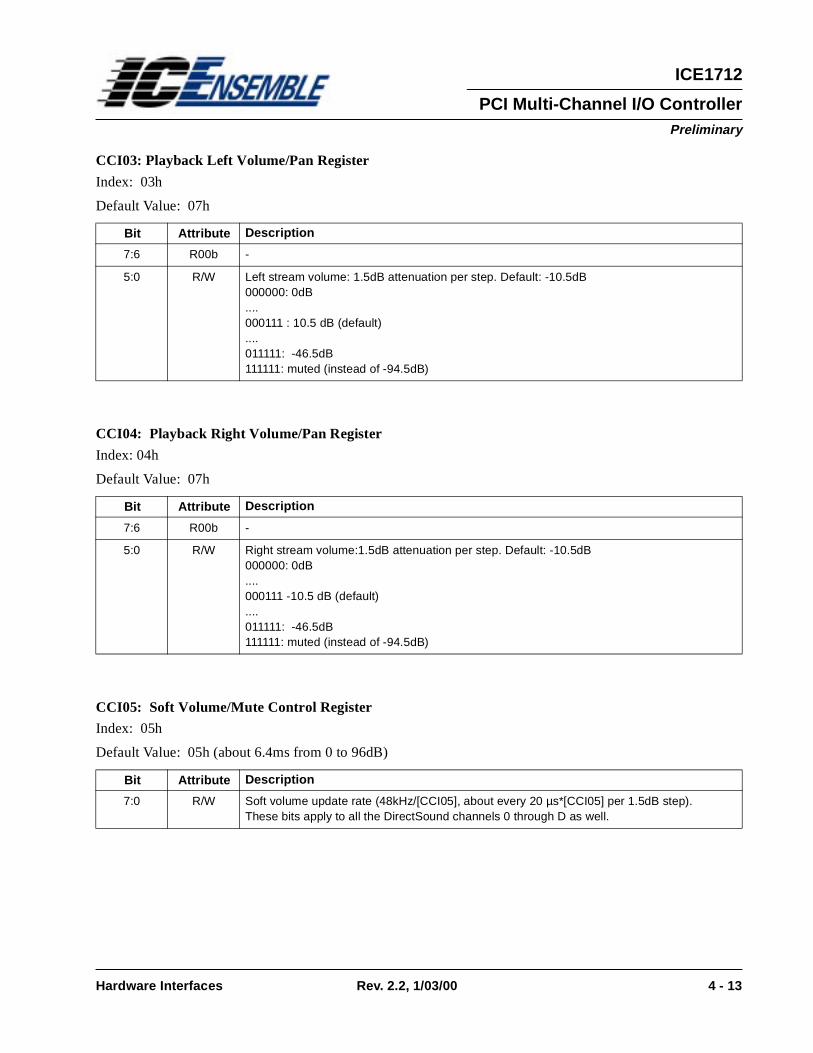
CCI03: Playback Left Volume/Pan Register
Index: 03h
Default Value: 07h
CCI04: Playback Right Volume/Pan Register
Index: 04h
Default Value: 07h
CCI05: Soft Volume/Mute Control Register
Index: 05h
Default Value: 05h (about 6.4ms from 0 to 96dB)
Bit Attribute Description
7:6 R00b -
5:0 R/W Left stream volume: 1.5dB attenuation per step. Default: -10.5dB 000000: 0dB....000111 : 10.5 dB (default)....011111: -46.5dB111111: muted (instead of -94.5dB)
Bit Attribute Description
7:6 R00b -
5:0 R/W Right stream volume:1.5dB attenuation per step. Default: -10.5dB000000: 0dB....000111 -10.5 dB (default)....011111: -46.5dB111111: muted (instead of -94.5dB)
Bit Attribute Description
7:0 R/W Soft volume update rate (48kHz/[CCI05], about every 20 µs*[CCI05] per 1.5dB step).These bits apply to all the DirectSound channels 0 through D as well.

4 - 14 Rev. 2.2, 1/03/00 Hardware Interfaces
PCI Multi-Channel I/O Controller
ICE1712
Preliminary
CCI06: Playback Sampling Rate Register (Low Byte)
Index: 06h
Default Value: 0xFFh
Note: SR, consumer mode (WAV PCM on Channel E and F) Sampling Rate is a 20-bit value programmed among registersCCI06 through CCI08. SR = fs* 220/48000. This has the resolution of less than 1Hz. When it is programmed to (220 -1),sampling rate will be rounded to 48kHz exactly.
CCI07: Playback Sampling Rate Register (Middle Byte)
Index: 07h
Default Value: 0xFFh
CCI08: Playback Sampling Rate Register (High Byte)
Index: 08h
Default Value: 0x0Fh
CCI10: Record Current/Base Terminal Count Register (High Byte)
Index: 10h
Default Value: 00h
Bit Attribute Description
7:0 R/W see note below.
Bit Attribute Description
7:0 R/W see note under CCI06.
Bit Attribute Description
7:4 R0h -
3:0 R/W see note under CCI06.
Bit Attribute Description
7:0 WO Write the high byte record terminal count in bytes. Like register CCS18, this register also auto-decrements as the DMA transfer progresses. When it reaches 0, it generates and interrupt. Program the desired count in dword units minus one to determine the interrupt frequency desired.
Hardware Interfaces Rev. 2.2, 1/03/00 4 - 15
PCI Multi-Channel I/O Controller
ICE1712
Preliminary
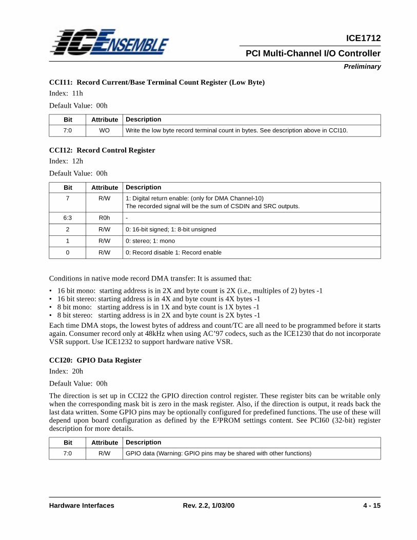
CCI11: Record Current/Base Terminal Count Register (Low Byte)
Index: 11h
Default Value: 00h
CCI12: Record Control Register
Index: 12h
Default Value: 00h
Conditions in native mode record DMA transfer: It is assumed that:
• 16 bit mono: starting address is in 2X and byte count is 2X (i.e., multiples of 2) bytes -1• 16 bit stereo: starting address is in 4X and byte count is 4X bytes -1• 8 bit mono: starting address is in 1X and byte count is 1X bytes -1• 8 bit stereo: starting address is in 2X and byte count is 2X bytes -1Each time DMA stops, the lowest bytes of address and count/TC are all need to be programmed before it startsagain. Consumer record only at 48kHz when using AC’97 codecs, such as the ICE1230 that do not incorporateVSR support. Use ICE1232 to support hardware native VSR.
CCI20: GPIO Data Register
Index: 20h
Default Value: 00h
The direction is set up in CCI22 the GPIO direction control register. These register bits can be writable onlywhen the corresponding mask bit is zero in the mask register. Also, if the direction is output, it reads back thelast data written. Some GPIO pins may be optionally configured for predefined functions. The use of these willdepend upon board configuration as defined by the E²PROM settings content. See PCI60 (32-bit) registerdescription for more details.
Bit Attribute Description
7:0 WO Write the low byte record terminal count in bytes. See description above in CCI10.
Bit Attribute Description
7 R/W 1: Digital return enable: (only for DMA Channel-10)The recorded signal will be the sum of CSDIN and SRC outputs.
6:3 R0h -
2 R/W 0: 16-bit signed; 1: 8-bit unsigned
1 R/W 0: stereo; 1: mono
0 R/W 0: Record disable 1: Record enable
Bit Attribute Description
7:0 R/W GPIO data (Warning: GPIO pins may be shared with other functions)

4 - 16 Rev. 2.2, 1/03/00 Hardware Interfaces
PCI Multi-Channel I/O Controller
ICE1712
Preliminary
CCI21: GPIO Write Mask Register
Index: 21h
Default Value: FFh
CCI22: GPIO Direction Control Register
Index: 22h
Default Value: 00h
For all bits 0: input; 1: output.
CCI30: Consumer Section Power Down Register
Index: 30h
Default Value: 00h
Bit Attribute Description
7:0 R/W GPIO write mask 0: Corresponding CCI20 register bit can be written. 1: Can NOT be written.
Bit Attribute Description
7 R/W GPIO7 direction. If 2nd MIDI UART in use, this bit will be read as 0 always.
6 R/W GPIO6 direction. If 2nd MIDI UART in use, this bit will be read as 1 always
5 R/W GPIO5 direction. If external clock synthesizer is used, this bit will be read as 1 always.
4 R/W GPIO4 direction. If external clock synthesizer is used, this bit will be read as 1 always.
3 R/W GPIO3 direction. During reset, this pin is used for E²PROM power-on strapping.
2 R/W GPIO2 direction. If TESTEN# pin is active, this pin is always input.
1:0 R/W GPIO1 and GPIO0 direction control register.
Bit Attribute Description
7 R/W 1: Crystal clock generation power down for XTAL_1
6 R/W 1: Game port analog power down
5 R/W Reserved.
4 R/W 1: Stop I²C port clock
3 R/W 1: Stop MIDI clock
2 R/W 1: Stop AC’97 clock
1 R/W 1: Stop DS Block clock
0 R/W 1: Stop PCI clock for SB, DMA controller (excluding PCI BIU, config. space and this register)

Hardware Interfaces Rev. 2.2, 1/03/00 4 - 17
PCI Multi-Channel I/O Controller
ICE1712
Preliminary
CCI31: Multi-Track Section Power Down Register
Index: 31h
Default Value: 00h
There are four power states defined in the PCI bus power management spec.
Bit Attribute Description
7 R/W 1: Crystal clock generation power down for XTAL_2
6:3 R/W Reserved
2 R/W 1: Stop S/PDIF clock
1 R/W 1: Stop Professional digital mixer clock
0 R/W 1: Stop Multi-track I²S serial interface clock
States Description
D0 Normal operation state after system power up or internal reset
D1 not supported.
D2 Power down all the blocks defined in the power down registers.
D3(hot) Same as D2 state, except a transition to D0 will generate an internal reset (incl. PCI config. space)
4 - 18 Rev. 2.2, 1/03/00 Hardware Interfaces
PCI Multi-Channel I/O Controller
ICE1712
Preliminary
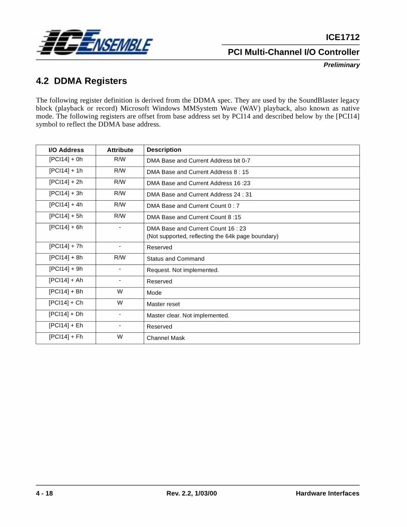
4.2 DDMA Registers
The following register definition is derived from the DDMA spec. They are used by the SoundBlaster legacyblock (playback or record) Microsoft Windows MMSystem Wave (WAV) playback, also known as nativemode. The following registers are offset from base address set by PCI14 and described below by the [PCI14]symbol to reflect the DDMA base address.
I/O Address Attribute Description
[PCI14] + 0h R/W DMA Base and Current Address bit 0-7
[PCI14] + 1h R/W DMA Base and Current Address 8 : 15
[PCI14] + 2h R/W DMA Base and Current Address 16 :23
[PCI14] + 3h R/W DMA Base and Current Address 24 : 31
[PCI14] + 4h R/W DMA Base and Current Count 0 : 7
[PCI14] + 5h R/W DMA Base and Current Count 8 :15
[PCI14] + 6h - DMA Base and Current Count 16 : 23(Not supported, reflecting the 64k page boundary)
[PCI14] + 7h - Reserved
[PCI14] + 8h R/W Status and Command
[PCI14] + 9h - Request. Not implemented.
[PCI14] + Ah - Reserved
[PCI14] + Bh W Mode
[PCI14] + Ch W Master reset
[PCI14] + Dh - Master clear. Not implemented.
[PCI14] + Eh - Reserved
[PCI14] + Fh W Channel Mask
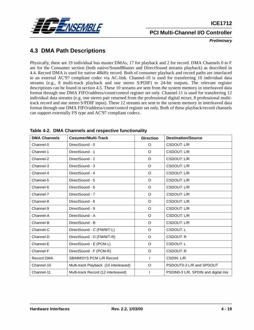
Hardware Interfaces Rev. 2.2, 1/03/00 4 - 19
PCI Multi-Channel I/O Controller
ICE1712
Preliminary
4.3 DMA Path Descriptions
Physically, there are 19 individual bus master DMAs, 17 for playback and 2 for record. DMA Channels 0 to Fare for the Consumer section (both native/SoundBlaster and DirectSound streams playback) as described in4.4. Record DMA is used for native 48kHz record. Both of consumer playback and record paths are interfacedto an external AC'97 compliant codec via AC-link. Channel-10 is used for transferring 10 individual datastreams (e.g., 8 multi-track playback and one stereo S/PDIF) to 24-bit outputs. The relevant registerdescriptions can be found in section 4.5. These 10 streams are sent from the system memory in interleaved dataformat through one DMA FIFO/address/count/control register set only. Channel-11 is used for transferring 12individual data streams (e.g. one stereo pair returned from the professional digital mixer, 8 professional multi-track record and one stereo S/PDIF input). These 12 streams are sent to the system memory in interleaved dataformat through one DMA FIFO/address/count/control register set only. Both of these playback/record channelscan support externally I²S type and AC'97 compliant codecs.
Table 4-2. DMA Channels and respective functionality
DMA Channels Cosumer/Multi-Track Direction Destination/Source
Channel-0 DirectSound - 0 O CSDOUT: L/R
Channel-1 DirectSound - 1 O CSDOUT: L/R
Channel-2 DirectSound - 2 O CSDOUT: L/R
Channel-3 DirectSound - 3 O CSDOUT: L/R
Channel-4 DirectSound - 4 O CSDOUT: L/R
Channel-5 DirectSound - 5 O CSDOUT: L/R
Channel-6 DirectSound - 6 O CSDOUT: L/R
Channel-7 DirectSound - 7 O CSDOUT: L/R
Channel-8 DirectSound - 8 O CSDOUT: L/R
Channel-9 DirectSound - 9 O CSDOUT: L/R
Channel-A DirectSound - A O CSDOUT: L/R
Channel-B DirectSound - B O CSDOUT: L/R
Channel-C DirectSound - C (FM/WT-L) O CSDOUT: L
Channel-D DirectSound - D (FM/WT-R) O CSDOUT: R
Channel-E DirectSound - E (PCM-L) O CSDOUT: L
Channel-F DirectSound - F (PCM-R) O CSDOUT: R
Record DMA SB/MMSYS PCM L/R Record I CSDIN: L/R
Channel-10 Multi-track Playback (10 interleaved) O PSDOUT0-3 L/R and SPDOUT
Channel-11 Multi-track Record (12 interleaved) I PSDIN0-3 L/R, SPDIN and digital mix

4 - 20 Rev. 2.2, 1/03/00 Hardware Interfaces
PCI Multi-Channel I/O Controller
ICE1712
Preliminary
4.4 Consumer Section DMA Channel Registers
The following registers are offset from base address set by PCI18. The DSx registers are located at [PCI18]+x.The 16 bytes I/O space controls the consumer section DMA channels for DOS legacy, native and DirectSound.
Table 4-3. DSx Consumer DMA Channel Register Map
DS0: DirectSound DMA Interrupt Mask Register:
Address Offset: 00 - 01h
Default Value: 3FFFh
DS2: DirectSound DMA Interrupt Status Register:
Address Offset: 02 - 03h
Default Value: 0000h
DS4: Channel Data Register:
Address Offset: 04h - 07h
Default Value: 00000000h.
Byte 3 Byte 2 Byte 1 Byte 0 Offset (Hex)
DirectSound DMA Interrupt Status DirectSound DMA Interrupt Mask 00
Channel Data 04
- Channel Index 08
- 0C
Bit Attribute Description
15:14 R00b -
13:00 R/W Each bit corresponding to the interrupt mask for each channel (0 to D). Default is masked.
Bit Attribute Description
15:14 R00b -
13:0 R/WC/ Each bit corresponding to the interrupt status of each channel (0 to D)These are sticky bits. The driver needs to clear by writing a 1 to the corresponding bit.
Bit Attribute Description
31:0 R/W Channel Data register. See 32-bit index register description after Table 4-4.

Hardware Interfaces Rev. 2.2, 1/03/00 4 - 21
PCI Multi-Channel I/O Controller
ICE1712
Preliminary
DS8: Channel Index Register
Address Offset: 08h
Default Value: 00h
Note: • When the playback enable bit is changed from 0 to 1 (in Index 4 bit 0), the first active buffer will be from
buffer 0. Before this, the return active address and count will not be updated.Conditions in DMA transfer:
• 16 bit mono: starting address is in 2X and count is multiple of 2X bytes (-1)• 16 bit stereo: starting address is in 4X and count is multiple of 4X bytes (-1)• 8 bit mono: starting address is in 1X and count is multiple of 1X bytes (-1)• 8 bit stereo: starting address is in 2X and count is multiple of 2X bytes (-1)
Bit Attribute Description
7:4 R/W Channel number. Valid only from Channel-0 to D. E and F are reserved for PCM streams regardless whether running in native or SB mode.
3:0 R/W Channel Index register. The table below is used for command decoding purposes.
Table 4-4. DS8 Register, Low Nibble Index Description Applicable to Channel-0 through D
Index Attribute Description
0h R/W Bits [27:0]W: Buffer_0 DMA base address[27:0] R: current active DMA buffer address[27:0]. Byte address.
1h R/W Bits [15:0] W: Buffer_0 DMA base count [15:0] R: current active DMA count [15:0]. Program byte count minus one.
2h R/W Bits[27:0] W: Buffer_1 DMA base address bit [27:0] R: same as in index 0h. Byte address
3h R/W Bits [15:0] W: Buffer_1 DMA base count [15:0] R: same as in index 1h. Program byte count minus one.
4h R/W Bits [7:0] R/W: Channel Control and Status register.
5h R/W Bits [19:0] Channel Sampling Rate
6h R/W Bits [13:0] (see note below) Channel left and right volume/pan control

4 - 22 Rev. 2.2, 1/03/00 Hardware Interfaces
PCI Multi-Channel I/O Controller
ICE1712
Preliminary
Channel Control and Status Register at Index 4h (DS8 = x4h)
Default: 00000060h
Consumer mode Sampling Rate Register at Index 5h (DS8 = x5h)
Index: 05h
Default Value: 0x000FFFFFh (48kHz)
Bit Attribute Description
31:8 R000h -
7 RO 1: indicating that the current active buffer is Buffer_1.0: indicating that the current active buffer is Buffer_0.To avoid the case of reading this bit during the transition, it is recommended that driver read this bit in the ISR so that the returned address and count are in-sync. with the buffer status.
6 R/W 0: Buffer_1 auto init. disable (single block mode)1: Buffer_1 auto init. enable (loop mode), default.
5 R/W 0: Buffer_0 auto init. disable (single block mode)1: Buffer_0 auto init. enable (loop mode ), default.
4 R/W Flush FIFO
3 R/W 1: stereo; 0: mono (default).For the DirectSound path this bit is only valid and can be programmed in the even number of channels, i.e., 0,2,4..,C. The second data element will be routed to the next odd slot into the internal SRC core. Driver should not program the odd number channel address and count etc. since it is occupied. (sampling rate and volume should still be programmed, however).
2 RW Consumer mode data format:0: 16-bit signed; 1: 8-bit unsigned
1 RW DMA request 1:pause
0 RW DMA request 1: start, 0:stop
Bit Attribute Description
31:20 R0 -
19:00 R/W SR: Sampling Rate for all DirectSound streams (except Channel E and F, see CCI06) is a 20-bit value. SR = fs* 220/48000. This has the resolution of less than 1Hz. When it is programmed to (220 -1), sampling rate will be rounded to 48kHz exactly.

Hardware Interfaces Rev. 2.2, 1/03/00 4 - 23
PCI Multi-Channel I/O Controller
ICE1712
Preliminary
Consumer mode Left/Right Volume Register at Index 06h (DS8 = x6h)
Index: 06h
Default: 00000707h
Note:
Channels E and F are dedicated for consumer PCM left and right streams respectively for either MicrosoftWindows MMSystem Wave (WAV) or SoundBlaster. In the MMSystem mode, the sampling rate and thevolume are defined in the CCS3 and CCS4 index registers. In the SB mode, the sampling rate is coming fromSB command and volume is defined in the SB mixer registers.
Channel C and D are dedicated for FM synthesis output left and right streams respectively in the SB mode. Inthis case, the FM volume will be coming from the SB mixer register space setting. The sampling rate, however,is determined from the above DS8 index registers.
Table 4-5. Channel parameter controls
Bit Attribute Description
31:14 R0 -
13:8 R/W Right volume:1.5dB attenuation per step. 000000: 0dB....000111: -10.5 dB (default)....011111: -46.5dB....111111: muted (instead of -94.5dB)
7:6 R0 -
5:0 R/W Left volume :1.5dB attenuation per step. Default: -10.5dB. Same table as in Right volume.
Channels Mode Data Interrupt status bit Volume Control Sampling Frequency
E:F Legacy DOS SB PCM INTA# (routing) SB mixer register SB command
C:D Legacy DOS FM NMI: for I/O trapping INTA# or NMI for data transfer
SB mixer register DS8, index register 5 Programmed by TSR
C:D Legacy DOS WT Same as above DS8=x6h CCS00_4=1b Same as above.
E:F Native Native PCM INTA#: CCS02 CCS03, CCS04 SE index registers 6-8
C:D Native Native FM/WT INTA#: DS2, DS3 DS8, index register 6 DS8, index register 5

4 - 24 Rev. 2.2, 1/03/00 Hardware Interfaces
PCI Multi-Channel I/O Controller
ICE1712
Preliminary
4.5 Professional Multi-Track Control Registers
The following registers are offset from base address set by PCI1C. The MTxx registers are located at[PCI1C]+xx. The 64 bytes I/O space controls the professional multi-track record and playback, audio streamrouting, digital mixer and related output capability. Refer to Table 4-2 on page 19 of this chapter for a concisedescription of the DMA channels involved.
Table 4-6. MTxx Controller Register Map
4.5.1 Multi-Track Mode Control Registers
MT00: Professional section DMA Interrupt Mask and Status Register:
Address Offset: 00h
Default Value: C0h
This register relates to both Channel-10 and 11 (Professional playback and record). When DMAs are stopped,the last latched value is retained.This “DC” value may affect the digital mixer operation.
Byte 3 Byte 2 Byte 1 Byte 0 Offset (Hex)
- I²S data format Sampling Rate Select. DMA Int. Mask/Status 00
Professional section AC ‘97 Data Port P. AC ‘97 Comm./Stat. Prof. AC ‘97 Index 04
- 08
- 0C
Professional Playback DMA Current/Base Address 10
P. Playback DMA Current/Base Terminal Count Prof. Playback DMA Current/Base Count 14
- P. Playback Control 18
- 1C
Professional Record DMA Current/Base Address 20
P. Record DMA Current/Base Terminal Count Prof. Record DMA Current/Base Count 24
- P. Record Control 28
- 2C
Routing control to SPDOUT Routing control to PSDOUT[3:0] 30
Captured data Routing Selection 34
Volume Control Rate Vol. Control Ch. Index L/R Volume Control 38
Peak meter data Peak meter index - Mixer monitor return 3C
Bit Attribute Description
7 R/W Multi-track record interrupt mask
6 R/W Multi-track playback interrupt mask
5:2 R0 -
1 R/W/C Multi-track record interrupt status. Write a 1 to clear.

Hardware Interfaces Rev. 2.2, 1/03/00 4 - 25
PCI Multi-Channel I/O Controller
ICE1712
Preliminary
MT01: Professional section Sampling Rate Select Register:
Address Offset: 01h
Default Value: 00h.
This register applies to both Channel-10 and 11. For S/PDIF input, correct sampling rate must be set as well.See Figure 4-3 and Figure 4-4 on page 27 and page 28 respectively, in this chapter
0 R/W/C Multi-track playback interrupt status. Write a 1 to clear.
Bit Attribute Description
7:5 R000b -
4 R/W S/PDIF input clock as the master. 0: disabled1: enabled. S/PDIF receiver chip provides the master clock through SPMCLKIN (pin 111)Note that in this mode, 256X is the highest master clock available while the AC’97 MCLK requires 512X. IC Ensemble AC’97 codecs, such as the ICE1230 are designs based on BCLK which uses MCLK/2, i.e. 256X. When S/PDIF provides the master clock, if IC Ensemble AC’97 codecs are used, before setting S/PDIF as the master clock, proceed to switching the primary codec into slave mode (refer to the ICE1230 datasheet). In this mode PBCLK will be output from Envy24.
3:0 R/W Codec sampling rate select:All multi-track channels are set to the same rate. These bits are ignored if S/PDIF input is master. 0000: 48kHz0001: 24kHz0010: 12kHz0011: 9.6kHz0100: 32kHz0101: 16kHz0110: 8kHz0111: 96kHz1111: 64kHz 1000: 44.1kHz 1001: 22.05kHz1010: 11.025kHz1011: 88.2kHz others: reserved
Bit Attribute Description

4 - 26 Rev. 2.2, 1/03/00 Hardware Interfaces
PCI Multi-Channel I/O Controller
ICE1712
Preliminary
MT02: Professional codec I²S Data Format Register:
Address Offset: 02h
Default Value: 00h
See Figure 4-2 below for a timing diagram for bits [1:0]. See Figure 4-3 and Figure 4-4 on page 27 and page28 respectively for the visual description of other bits.
Figure 4-2. I²S Format Timing Diagram
MT04: Index Register for AC’97 Codecs on Professional section
Address Offset: 04h
Default Value: 00h
Bit Attribute Description
7:4 R0 -
3 R/W MCLK/LRCLK ratio, 0: 256x (default)1: 128x
2 R/W SCLK/LRCLK ratio, i.e. bpf (bits per frame, each frame corresponding to 1/SR) Typically useful for 44.1kHz sampling rate and its multiples where converters use 384X oversampling. If S/PDIF is used as reflected in PCI63_0 or 1, 64bpf mode is forced and this bit is rendered inactive.0: 64bpf (32/32) default. (PMCLK on pin 85 is 256 * LRCLK) 1: 48bpf (24/24) (PMCLK is 384 * LRCLK)
1:0 R/W Data format: 00: I²S (timing diagram provided below) others: Reserved
Bit Attribute Description
7 R0 -
6:0 R/W AC’97 registers Index. Refer to the AC’97 specification for register descriptions.
PBCLK/SPSCLK
PSYNC/SPSYNC Left Right
MSB LSB MSB LSB MSBPSDIN[0:3]
PSDOUT[0:3]SPDIN
SPDOUT

Hardw
are InterfacesR
ev. 2.2, 1/03/004 - 27
PC
I Multi-C
hannel I/O C
ontroller
ICE
1712
Prelim
inary
Figure 4-3. C
rystals to Master C
locks clock generation tree
149152
1 2
P M C L K(p in 85 )
S PM C L K IN(p in 111)
X IN 1(p in 64) divide by
MT01_[3:0]
fsp = P ro sam p ling ra te
S P* = S /P D IF I²S po rt
P * = P ro sec tion
256 fsp
M PU -401 and
SC L K(p in 71 )
M ID I T X /R X ra te
1, 2, 3, 4, 6, 8, 10, 12
MT01_4=0
M aster
S lave
1 2
1 256
C S Y N C(p in 88 )
C B C LK(p in 90 )
C M C L K(p in 92 )
fsc
256 fsc512 fsc
fsc = C onsum er sam p ling ra te
C * = C onsum er sec tion
G am e Port log ic
1 8
divide by1, 2, 4, 8
X IN 2(p in 60 )
MT02_3=1
MT02_3=0
1 2
1 3
IRU#6;7;#DQG63',)#DEVHQW
589;
MT01_4=1
PCI60[7:6]=01 &PCI63[1:0]=00

4 - 28 Rev. 2.2, 1/03/00 Hardware Interfaces
PCI Multi-Channel I/O Controller
ICE1712
Preliminary
Figure 4-4. Master Clocks to Bit Clocks, L/R Clocks and Sync generation
f sp
= P
ro s
am
pli
ng
ra
te
SP
* =
S/P
DIF
I²S
po
rt
P*
= P
ro s
ec
tio
n
PS
YN
C(p
in 7
2)
PB
CL
K(p
in 7
8)
PM
CL
K(p
in 8
5)
1
21
6
4
SP
SY
NC
(pin
10
9)
SP
SC
LK
(pin
11
0)
SP
MC
LK
OU
T(p
in 1
12
)
f sp
f sp
64
f sp
12
8f s
p
1
41
2
MT
01_4
= 1
or
MT
02_3
= 1
PC
I61_
7 =
0
MT
02_3
= 0
1
2M
T02
_3 =
1 &
MT
01_4
= 1
& P
CI6
1_7
= 0
PC
I61_
7 =
1
1
4(M
T02
_3 =
0 o
r
& P
CI6
1_7
= 1
1
8M
T02
_3 =
1 &
PC
I61_
7 =
1
PC
I60_
6 =
0)
1
48
MT
02_2
= 1
&P
CI6
3[1:
0] =
00b
1
64
MT
02_2
= 0
1 2
56
PC
I61_
7 =
0
IRU#6;7;#DQG#63',)#DEVHQW
GHIDXOW#+589;#RU#45;;,
IRU#$&¶<:#PRGH#RQO\
IRU#$&¶<:#PRGH#RQO\
GHIDXOW#589;#0&/.
RU#63',)#LQ#PDVWHU
45;;#0&/.

Hardware Interfaces Rev. 2.2, 1/03/00 4 - 29
PCI Multi-Channel I/O Controller
ICE1712
Preliminary
MT05: Command and Status Register for AC’97 Codecs on Professional Section
Address Offset: 05h
Default Value: 00h
MT06: Data Port Register for AC’97 codecs on Professional section
Address Offset: 06h - 07h
Default Value: 00h
Bit Attribute Description
7 R/W Cold reset. Write 1 to assert PRST# (pin105) active. Write back 0 to remove reset condition from all professional section codecs.
6 R/W Warm reset. Write 1 to have warm reset by asserting PSYNC (pin 72). This bit together with PRST# (pin 105) active (MT05_7=1) can be used to set the external IC Ensemble primary AC’97 codec to slave mode (such as the ICE1230). This must be done when S/PDIF input is the master. Apply Cold reset to restore codec master mode.
5 R/W Write 1 to write to AC’97 codec register Reading a 1 indicates the write cycle is still in progress, cleared when write cycle complete.
4 R/W Write 1 to read AC’97 CODEC register Reading a 1 indicates the read cycle is still in progress, cleared when there is valid data.
3 RO AC’97 codec ready status bit. After power-on, check that this bit is 1 before accessing codec registers.
2 R0b -
1:0 R/W ID for external AC’97 registers read/write. 00: select primary AC’97 codec.01: select second slave AC’97 codec.10: select third slave AC’97 codec.11: select fourth slave AC’97 codec.
Bit Attribute Description
15:8 R/W AC’97 codec register data high byte (index 07h) Refer to the AC’97 specification for register descriptions..
7:0 R/W AC’97 codec register data low byte (index 06h). Refer to the AC’97 specification for register descriptions.

4 - 30 Rev. 2.2, 1/03/00 Hardware Interfaces
PCI Multi-Channel I/O Controller
ICE1712
Preliminary
4.5.2 Multi-Track Playback Registers
The following figure is a visual representation of the multi-track data transfer mechanism. A ping-pong buffer structure is implemented for a seamless flow of multiple streams. 32-bit data transfers areused regardless of the audio data resolution. All transfer data are left (MSB) justified. Each transferrequest results into a PCI bus master burst cycle.
Figure 4-5. Multi-track DMA transfer diagram
MT10: Professional Section Playback DMA Current/Base Address Register
Index: 10h - 13h
Default Value: 00000000h. Channel-10 interleaves 10 slots, each with 32-bit from the system memory.
Bit Attribute Description
31:28 R0h - (Address space beyond 256MB is not supported)
27:2 R/W Write the Playback DMA base address in dword units (up to 256 MB address space supported) Read current address in dword units.
1:0 R00b - (This DMA channel supports dword boundary only)
3 2 1 0Byte Lanes 3 2 1 0
1 2 3 4 5 6 7 8 910
Stream/Track
Stream/Track
121110 9 8 7 6 5 4 3 2 1
PCI
DMA Channel-10 (Playback) DMA Channel-11 (Record)
to physical outputsfrom physical inputs

Hardware Interfaces Rev. 2.2, 1/03/00 4 - 31
PCI Multi-Channel I/O Controller
ICE1712
Preliminary
MT14: Professional Section Playback DMA Current/Base Count Register
Index: 14h - 15h
Default Value: 0000h
MT16: Professional Section Playback Current/Base Terminal Count Register
Index: 16 - 17h
Default Value: 0000h
MT18: Professional Section Playback and Record Control Register
Index: 18h
Default Value: 00h.
Bit Attribute Description
15:0 R/W Write the Playback DMA initial buffer size in dword units minus one. This register auto-decrements as the DMA transfer progresses. It reinitializes automatically to the original buffer size once it reaches 0 count.Read the current Playback DMA pointer.
Bit Attribute Description
15:0 WO Write the terminal count. This register also auto-decrements as the DMA transfer progresses. When it reaches 0, it generates and interrupt. Program the desired count in dword units minus one to determine the interrupt frequency desired.
Bit Attribute Description
7:3 R0 -
2 R/W 1: Record start; 0: Record stop. Shadowed in MT28_0.
1 R/W 1: Pause; 0: Resume
0 R/W 1: Playback start; 0: Playback stop

4 - 32 Rev. 2.2, 1/03/00 Hardware Interfaces
PCI Multi-Channel I/O Controller
ICE1712
Preliminary
4.5.3 Multi-Track Record Registers
MT20: Professional Section Record DMA Current/Base Address Register
Index: 20h - 23h
Default Value: 00000000h. Channel-11 interleaves 12 slots, each with 32-bit data to the system memory.
MT24: Professional Section Record DMA Current/Base Count Register
Index: 24 - 25h
Default Value: 0000h
MT26: Professional Section Record Current/Base Terminal Count Register
Index: 26h - 27h
Default Value: 0000h
MT28: Professional Section Record Control Register
Index: 28h
Default Value: 00h
Bit Attribute Description
31:28 R0h - (Address space beyond 256MB is not supported)
27:2 R/W Write the Playback DMA base address in dword units (up to 256 MB address space supported) Read current address in dword units.
1:0 R00b - (This DMA channel supports dword boundary only)
Bit Attribute Description
15:0 R/W Write the Record DMA initial buffer size in dword units minus one. This register auto-decrements as the DMA transfer progresses. It reinitializes automatically to the originalbuffer size once it reaches 0 count.Read the current Record DMA pointer after having allowed at least 2 sample frames.
Bit Attribute Description
15:0 WO Write the terminal count. This register also auto-decrements as the DMA transfer progresses. When it reaches 0, it generates and interrupt. Program the desired count in dword units minus one to determine the interrupt frequency desired.
Bit Attribute Description
7:1 R0 -
0 R/W 1: Record start; 0: Record stop. Same functionality as MT18_2

Hardware Interfaces Rev. 2.2, 1/03/00 4 - 33
PCI Multi-Channel I/O Controller
ICE1712
Preliminary
4.5.4 Professional Section Digital Loopback
The Envy24 provides an extensive routing capability of the data streams. The following registers control therouting from numerous sources to various destination. Insertion of the stream routing functionality adds a max-imum of a single sample cycle delay with respect to the original data. The switch matrix being so complex,careful register setting is crucial to avoid undesirable effects. For simplicity of the register description only pinnames are used. Refer to the pin list for pin numbers and location. The diagram below is a visual representation of possible connection. If a dot is missing on an intersection, itreflects the lack of routing capabitlity.
Figure 4-6. Data stream routing capabilities
Slot 1Slot 2Slot 3Slot 4Slot 5Slot 6Slot 7Slot 8Slot 9Slot10
Stream 1Stream 2Stream 3Stream 4Stream 5Stream 6Stream 7Stream 8Stream 9Stream10
D mix LD mix R
Str
eam
1S
trea
m 2
Str
eam
3S
trea
m 4
Str
eam
5S
trea
m 6
Str
eam
7S
trea
m 8
Str
eam
9S
trea
m1
0
Slo
t 1
Slo
t 2
Slo
t 3
Slo
t 4
Slo
t 5
Slo
t 6
Slo
t 7
Slo
t 8
Slo
t 9
Slo
t10
Slo
t11
Slo
t12
Co
nsu
mer
LC
on
sum
er R
Ou
tpu
t fro
m D
MA
Inpu
t fr
om
AD
C
Output to DAC Input to DMADestination
Sou
rce

4 - 34 Rev. 2.2, 1/03/00 Hardware Interfaces
PCI Multi-Channel I/O Controller
ICE1712
Preliminary
MT30: Routing Control Register for Data to PSDOUT[0:3]
Address Offset: 30h - 31h
Default Value: 00h
When PSDIN[0:3] or SPDIN are selected as the source, refer to register MT34.
Bit Attribute Description
15:14 R/W PSDOUT[3] Right source 00: from DMA Channel-10 output slot 8 01: - 10: from PSDIN[X] loopback 11: from SPDIN input loopback
13:12 R/W PSDOUT[2] Right source 00: from DMA Channel-10 output slot 6 01: - 10: from PSDIN[X] loopback 11: from SPDIN input loopback
11:10 R/W PSDOUT[1] Right source 00: from DMA Channel-10 output slot 4 01: - 10: from PSDIN[X] loopback 11: from SPDIN input loopback
9:8 R/W PSDOUT[0] Right source 00: from DMA Channel-10 output slot 2. 01: from digital mixer monitor Right output 10: from PSDIN[X] loopback 11: from SPDIN input loopback
7:6 R/W PSDOUT[3] Left source 00: from DMA Channel-10 output slot 7 01: - 10: from PSDIN[X] loopback 11: from SPDIN input loopback
5:4 R/W PSDOUT[2] Left source 00: from DMA Channel-10 output slot 5 01: - 10: from PSDIN[X] loopback 11: from SPDIN input loopback
3:2 R/W PSDOUT[1] Left source 00: from DMA Channel-10 output slot 3 01: - 10: from PSDIN[X] loopback 11: from SPDIN input loopback
1:0 R/W PSDOUT[0] Left source00: from DMA Channel-10 output slot 1 01: from digital mixer monitor Left output 10: from PSDIN[X] loopback 11: from SPDIN input loopback

Hardware Interfaces Rev. 2.2, 1/03/00 4 - 35
PCI Multi-Channel I/O Controller
ICE1712
Preliminary
MT32: Routing Control Register for SPDOUT
Address Offset: 32h - 33h
Default Value: 0000h
When PSDIN[0:3] or SPDIN are selected as the source, refer to register 38h-3Bh.
Bit Attribute Description
15 R/W SPDIN input loop back to SPDOUT Right output 1: SPDIN Right input 0: SPDIN Left input
14 : 12 R/W PSDIN[X] input loop back to SPDOUT Right output 000: PSDIN[0]: L 001: PSDIN[0]: R 010: PSDIN[1]: L 011: PSDIN[1]: R 100: PSDIN[2]: L 101: PSDIN[2]: R 110: PSDIN[3]: L 111: PSDIN[3]: R
11 RW SPDIN input loop back to SPDOUT Left output 1: S/PDIF right input 0: S/PDIF left input
10:8 RW PSDIN[X] input loop back to SPDIOUT Left output 000: PSDIN[0]: L 001: PSDIN[0]: R 010: PSDIN[1]: L 011: PSDIN[1]: R 100: PSDIN[2]: L 101: PSDIN[2]: R 110: PSDIN[3]: L 111: PSDIN[3]: R
7:4 R0h -
3:2 R/W Source loop back to the SPDOUT Right output 00: from DMA Channel-10 slot 10 01: from digital mixer monitor Right output 10: from PSDIN[X] (defined in bits 14:12 of this register) 11: from SPDIN (defined in bit 15 of this register)
1:0 R/W Source loop back to the SPDOUT Left output 00: from DMA Channel-10 slot 9 01: from digital mixer monitor Left output 10: from PSDIN[X] (defined in bits 10:8 of this register) 11: from SPDIN (defined in bit 11 of this register)

4 - 36 Rev. 2.2, 1/03/00 Hardware Interfaces
PCI Multi-Channel I/O Controller
ICE1712
Preliminary
MT34: Captured (Recorded) data Routing Selection Register
Address Offset: 34 - 37h
Default Value: 00000000h.
Bit Attribute Description
31 R/W SPDIN input loopback to PSDOUT[3] Right slot 1: SPDIN Right input 0: SPDIN Left input
30:28 R/W PSDIN[X] loopback to PSDOUT[3] Right slot 000: PSDIN[0]: L 001: PSDIN[0]: R 010: PSDIN[1]: L 011: PSDIN[1]: R 100: PSDIN[2]: L 101: PSDIN[2]: R 110: PSDIN[3]: L 111: PSDIN[3]: R
27 R/W SPDIN input loopback to PSDOUT[3] Left slot 1: SPDIN Right input 0: SPDIN Left input
26:24 R/W PSDIN[X] loopback to PSDOUT[3] Left slot 000: PSDIN[0]: L 001: PSDIN[0]: R 010: PSDIN[1]: L 011: PSDIN[1]: R 100: PSDIN[2]: L 101: PSDIN[2]: R 110: PSDIN[3]: L 111: PSDIN[3]: R
23 R/W SPDIN input loopback to PSDOUT[2] Right slot 1: SPDIN Right input 0: SPDIN Left input
22:20 R/W PSDIN[X] loopback to PSDOUT[2] Right slot 000: PSDIN[0]: L 001: PSDIN[0]: R 010: PSDIN[1]: L 011: PSDIN[1]: R 100: PSDIN[2]: L 101: PSDIN[2]: R 110: PSDIN[3]: L 111: PSDIN[3]: R
19 R/W SPDIN input loopback to PSDOUT[2] Left slot 1: S/PDIF right input 0: S/PDIF left input
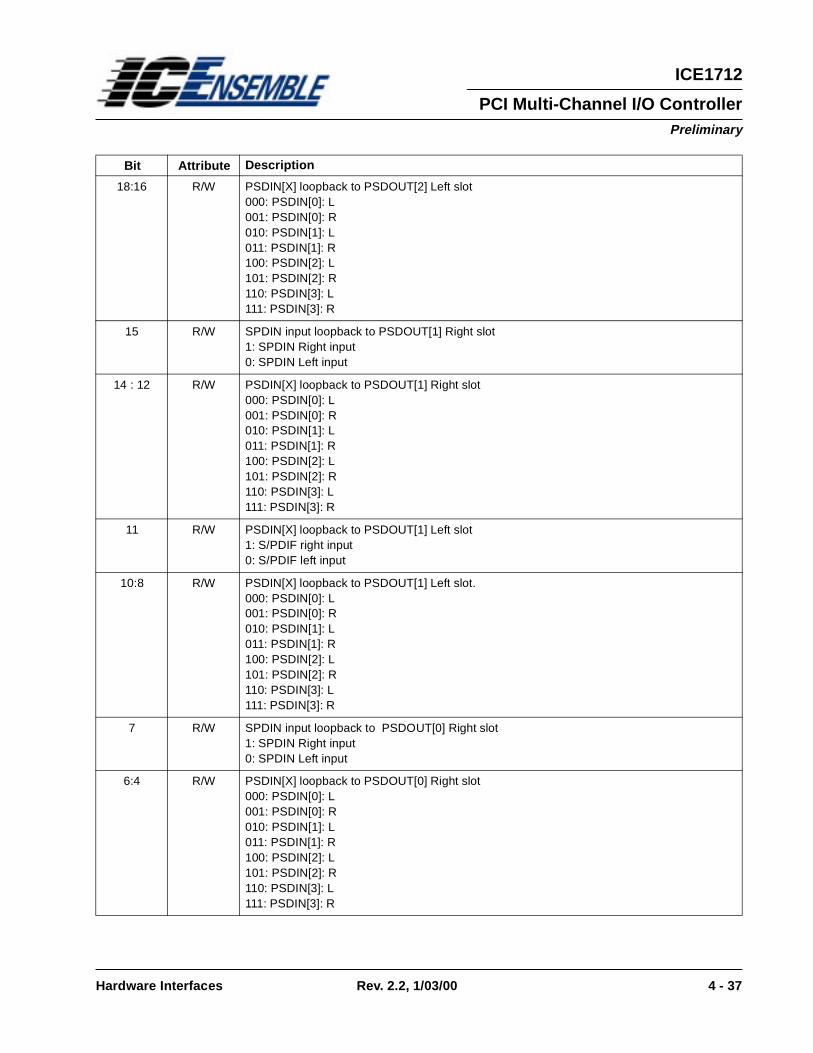
Hardware Interfaces Rev. 2.2, 1/03/00 4 - 37
PCI Multi-Channel I/O Controller
ICE1712
Preliminary
18:16 R/W PSDIN[X] loopback to PSDOUT[2] Left slot 000: PSDIN[0]: L 001: PSDIN[0]: R 010: PSDIN[1]: L 011: PSDIN[1]: R 100: PSDIN[2]: L 101: PSDIN[2]: R 110: PSDIN[3]: L 111: PSDIN[3]: R
15 R/W SPDIN input loopback to PSDOUT[1] Right slot 1: SPDIN Right input 0: SPDIN Left input
14 : 12 R/W PSDIN[X] loopback to PSDOUT[1] Right slot 000: PSDIN[0]: L 001: PSDIN[0]: R 010: PSDIN[1]: L 011: PSDIN[1]: R 100: PSDIN[2]: L 101: PSDIN[2]: R 110: PSDIN[3]: L 111: PSDIN[3]: R
11 R/W PSDIN[X] loopback to PSDOUT[1] Left slot 1: S/PDIF right input 0: S/PDIF left input
10:8 R/W PSDIN[X] loopback to PSDOUT[1] Left slot. 000: PSDIN[0]: L 001: PSDIN[0]: R 010: PSDIN[1]: L 011: PSDIN[1]: R 100: PSDIN[2]: L 101: PSDIN[2]: R 110: PSDIN[3]: L 111: PSDIN[3]: R
7 R/W SPDIN input loopback to PSDOUT[0] Right slot 1: SPDIN Right input 0: SPDIN Left input
6:4 R/W PSDIN[X] loopback to PSDOUT[0] Right slot 000: PSDIN[0]: L 001: PSDIN[0]: R 010: PSDIN[1]: L 011: PSDIN[1]: R 100: PSDIN[2]: L 101: PSDIN[2]: R 110: PSDIN[3]: L 111: PSDIN[3]: R
Bit Attribute Description

4 - 38 Rev. 2.2, 1/03/00 Hardware Interfaces
PCI Multi-Channel I/O Controller
ICE1712
Preliminary
3 R/W SPDIN input loopback to PSDOUT[0] Left slot 1: SPDIN Right input 0: SPDIN Left input
2:0 R/W PSDIN[X] loopback to PSDOUT[0] Left slot 000: PSDIN[0]: L 001: PSDIN[0]: R 010: PSDIN[1]: L 011: PSDIN[1]: R 100: PSDIN[2]: L 101: PSDIN[2]: R 110: PSDIN[3]: L 111: PSDIN[3]: R
Bit Attribute Description

Hardware Interfaces Rev. 2.2, 1/03/00 4 - 39
PCI Multi-Channel I/O Controller
ICE1712
Preliminary
4.5.5 Multi-Track Digital Monitoring
The Envy24 integrates a 36-bit resolution digital hardware mixer. The width of the data path is strictly toensure that during processing of all the channels, under any condition, no resolution is lost. The dynamic rangeof the end user system will be limited by the range of the physical output devices used. In order to maintainidentical gain to the input stream (i.e. 0dB), the resulting 24-bit is not msb-aligned to the 36-bit. The overflowbits correspond to the analog distortion due to saturation. The user would need to reduce the overall attenuationof the inputs to avoid clipping. Insertion of the digital mixer adds only a single sample cycle delay with respectto the original data. This extremely low latency all digital mixer provides monitoring functionality and canreplace a traditional external analog input mixer. There are 20 independent audio data streams to mix andcontrol the volume. The output destination of this mixer can be the consumer AC ‘97 codec, an external DACat PSDOUT[0] or SPDOUT or both simultaneously, as well as return to the host on slots 11 and 12 (the lasttwo) of DMA Channel-11. Refer to the registers MT30, MT32, MT34 and MT3Ch in section 4.5.4 about audiodata routing. Note that the consumer AC’97 path is limited to 48kHz sampling rate maximum and for sub-48kHz sampling rates, Channel-A and B of the DirectSound accelerator are allocated for SRC when the digitalmixer return stream is at a sample rate other than 48kHz. All other DirectSound streams operate concurrentlywithout alterations.
MT38: Left/Right Volume Control Data Register
Address Offset: 38 - 39h
Default Value: 0707h
Refer to MT3A register for the audio data channel selection.
Bits Attribute Description
15 R0b -
14:8 R/W Right Volume control. Same format as the in the left volume control.
7 R0b -
6:0 R/W Left volume control. 0000000: 0dB0000001: -1.5dB (0.841395141)0000010: -3.0dB (0.7079458)0000011: -4.5dB (0.5956621)....0000111: -10.5 dB (default)....0011111: -46.5dB....0111111: -94.5dB1000000: -96dB....1100000: -144dB (maximum attenuation)1111111: mute

4 - 40 Rev. 2.2, 1/03/00 Hardware Interfaces
PCI Multi-Channel I/O Controller
ICE1712
Preliminary
MT3A: Volume Control Stream Index Register:
Address Offset: 3Ah
Default Value: 00h
MT3B: Volume Control Rate Register
Address Offset: 3Bh
Default Value: 30h
This register allows gradual change of the digital mixer volume setting. The value in MT3B specifiesthe number of samples to elapse (in hex) between each 1.5dB increment/decrement in volume mixer.This gradual volume update continues until the setting programmed into MT38 is reached. The appro-priate value to program may vary, but 00 or 01h are good choices for most cases.
Bit Attribute Description
7:6 R00b -
5:0 R/W Index to select stream:00000: Playback stream 1 (Channel-10 slot 1)00001: Playback stream 2 (Channel-10 slot 2)00010: Playback stream 3 (Channel-10 slot 3)00011: Playback stream 4 (Channel-10 slot 4)00100: Playback stream 5 (Channel-10 slot 5)00101: Playback stream 6 (Channel-10 slot 6)00110: Playback stream 7 (Channel-10 slot 7)00111: Playback stream 8 (Channel-10 slot 8)01000: Playback stream 9 (Channel-10 slot 9, typ. S/PDIF Left output stream) 01001: Playback stream 10 (Channel-10 slot 10, typ. S/PDIF Right output stream) 01010: Record stream 1 (Channel-11 slot 1)01011: Record stream 2 (Channel-11 slot 2)01100: Record stream 3 (Channel-11 slot 3)01101: Record stream 4 (Channel-11 slot 4)01110: Record stream 5 (Channel-11 slot 5)01111: Record stream 6 (Channel-11 slot 6)10000: Record stream 7 (Channel-11 slot 7)10001: Record stream 8 (Channel-11 slot 8)10010: Record stream 9 (Channel-11 slot 9, typ. S/PDIF Left input stream) 10011: Record stream 10 (Channel-11 slot 10, typ. S/PDIF Right input stream) others: ignored.
Bits Attribute Description
7:0 R/W Volume update rate control (sampling rate, PSYNC)

Hardware Interfaces Rev. 2.2, 1/03/00 4 - 41
PCI Multi-Channel I/O Controller
ICE1712
Preliminary
MT3C: Digital Mixer Monitor Routing Control Register
Address Offset: 3Ch
Default Value: 00h
Figure 4-7. Digital Mixer Functional Diagram
Bits Attribute Description
7:6 R0 -
0 R/W 1: Route digital mixer output to the Consumer AC’97 path by allocating Channel-A and B.
ΣΣΣΣ
DMA Channel-10 DMA Channel-11(Playback) (Record)
slot 10slot 1.....slot 1..... slot 10
.... ....
36b 36b
24b 24b
24b
0dB
-144dB
Left Monitor Output(routing selection via MT30, MT32, MT3C)
0dB
-144dB
0dB
-144dB
0dB
-144dB
MT38 MT38
(Stream attenuator selection via MT3A)
ΣΣΣΣ
DMA Channel-10 DMA Channel-11(Playback) (Record)
slot 10slot 1.....slot 1..... slot 10
.... ....
36b 36b
24b 24b
24b
0dB
-144dB
Right Monitor Output(routing selection via MT30, MT32, MT3C)
-144dB
0dB
-144dB
0dB
-144dB
MT39 MT39
(Stream attenuator selection via MT3A)
0dB
Peak Peak Peak Peak PeakPeakPeak Peak
Peak PeakRead peaks via MT3E, MT3F

4 - 42 Rev. 2.2, 1/03/00 Hardware Interfaces
PCI Multi-Channel I/O Controller
ICE1712
Preliminary
MT3E: Peak Meter Index Register
Address Offset: 3Eh
Default Value: 00h
MT3F: Peak Meter Data Register
Address Offset: 3Fh
Default Value: 00h
Bits Attribute Description
7:5 R000b -
4:0 R/W Peak meter stream index00000: Playback stream 1 (Channel-10 slot 1)00001: Playback stream 2 (Channel-10 slot 2)00010: Playback stream 3 (Channel-10 slot 3)00011: Playback stream 4 (Channel-10 slot 4)00100: Playback stream 5 (Channel-10 slot 5)00101: Playback stream 6 (Channel-10 slot 6)00110: Playback stream 7 (Channel-10 slot 7)00111: Playback stream 8 (Channel-10 slot 8)01000: Playback stream 9 (Channel-10 slot 9, typ. S/PDIF Left output stream) 01001: Playback stream 10 (Channel-10 slot 10, typ. S/PDIF Right output stream) 01010: Record stream 1 (Channel-11 slot 1)01011: Record stream 2 (Channel-11 slot 2)01100: Record stream 3 (Channel-11 slot 3)01101: Record stream 4 (Channel-11 slot 4)01110: Record stream 5 (Channel-11 slot 5)01111: Record stream 6 (Channel-11 slot 6)10000: Record stream 7 (Channel-11 slot 7)10001: Record stream 8 (Channel-11 slot 8)10010: Record stream 9 (Channel-11 slot 9, typ. S/PDIF Left input stream) 10011: Record stream 10 (Channel-11 slot 10, typ. S/PDIF Right input stream) 10100: Record stream 11 (Channel-11 slot 11, typ. digital mixer monitor Left output stream) 10101: Record stream 12 (Channel-11 slot 12, typ. digital mixer monitor Right output stream)others: ignored.
Bits Attribute Description
7:0 R Peak data derived from the absolute value of 9 msb. 00h min - FFh max volume. Reading the register resets the meter to 00h.
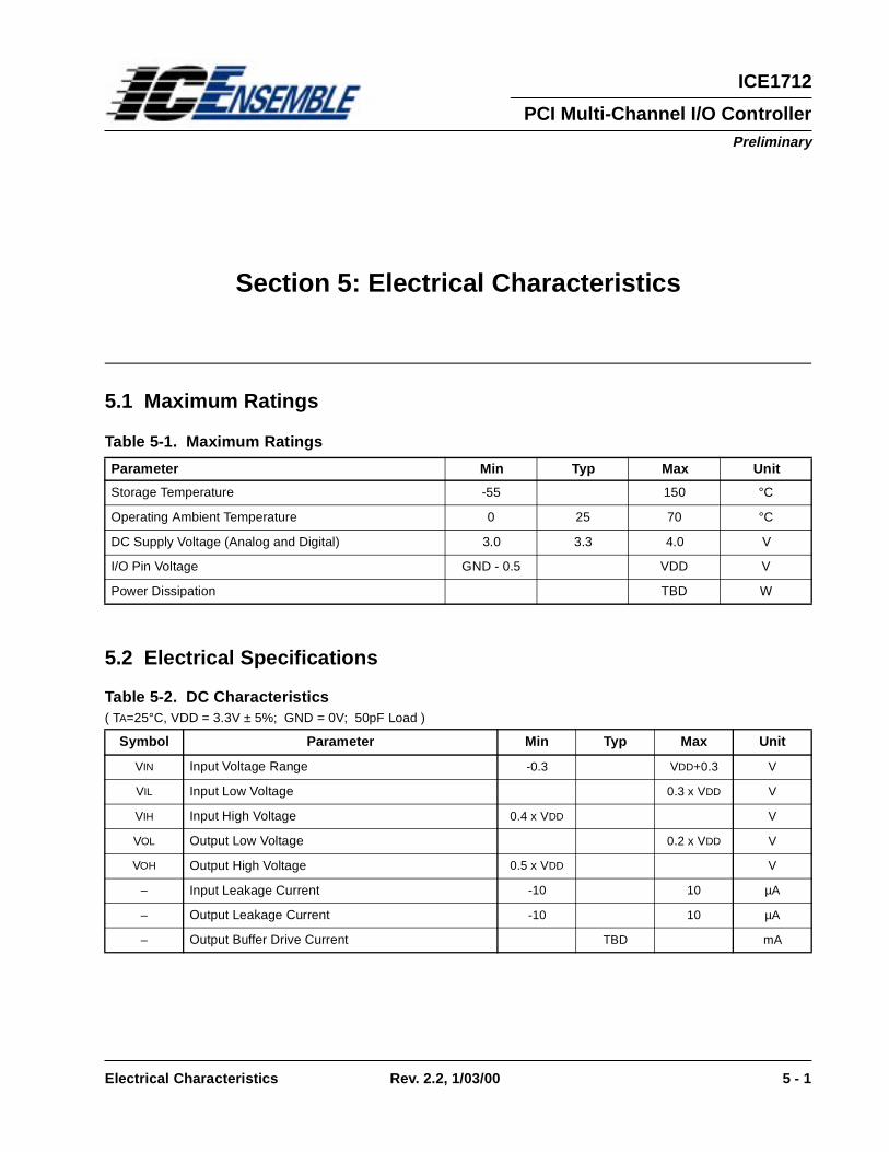
Electrical Characteristics Rev. 2.2, 1/03/00 5 - 1
PCI Multi-Channel I/O Controller
ICE1712
Preliminary
Section 5: Electrical Characteristics
5.1 Maximum Ratings
5.2 Electrical Specifications
Table 5-2. DC Characteristics( TA=25°C, VDD = 3.3V ± 5%; GND = 0V; 50pF Load )
Table 5-1. Maximum Ratings
Parameter Min Typ Max Unit
Storage Temperature -55 150 °C
Operating Ambient Temperature 0 25 70 °C
DC Supply Voltage (Analog and Digital) 3.0 3.3 4.0 V
I/O Pin Voltage GND - 0.5 VDD V
Power Dissipation TBD W
Symbol Parameter Min Typ Max Unit
VIN Input Voltage Range -0.3 VDD+0.3 V
VIL Input Low Voltage 0.3 x VDD V
VIH Input High Voltage 0.4 x VDD V
VOL Output Low Voltage 0.2 x VDD V
VOH Output High Voltage 0.5 x VDD V
– Input Leakage Current -10 10 µA
– Output Leakage Current -10 10 µA
– Output Buffer Drive Current TBD mA

5 - 2 Rev. 2.2, 1/03/00 Electrical Characteristics
PCI Multi-Channel I/O Controller
ICE1712
Preliminary
Table 5-3. Power Consumption( TA=25°C, VDD = 3.3V ± 5%; GND = 0V; 50pF Load )
5.3 AC Timing Characteristics(Test Conditions: TA=25°C, VDD = 3.3V ± 5%; GND = 0V; 50pF Load)
Table 5-4. Cold Reset
Figure 5-1. Cold Reset Timing
Symbol Parameter Min Typ Max Unit
IVDD Supply Current: Power Up 110 mA
IVDD Supply Current: Partial Power Up TBD mA
IVDD Supply Current: Partial Power Down TBD mA
IVDD Supply Current: Power Down TBD mA
Symbol Parameter Min Typ Max Unit
TRST_LOW CRST#/PRST# Active Low Pulse Width 1 µs
TRST2CLKCRST#/PRST# Inactive to CBLK/PBCLK/SPSCLKStartup Delay 162.8 ns
TRST_LOW TRST2CLK
xRST#
xxCLK
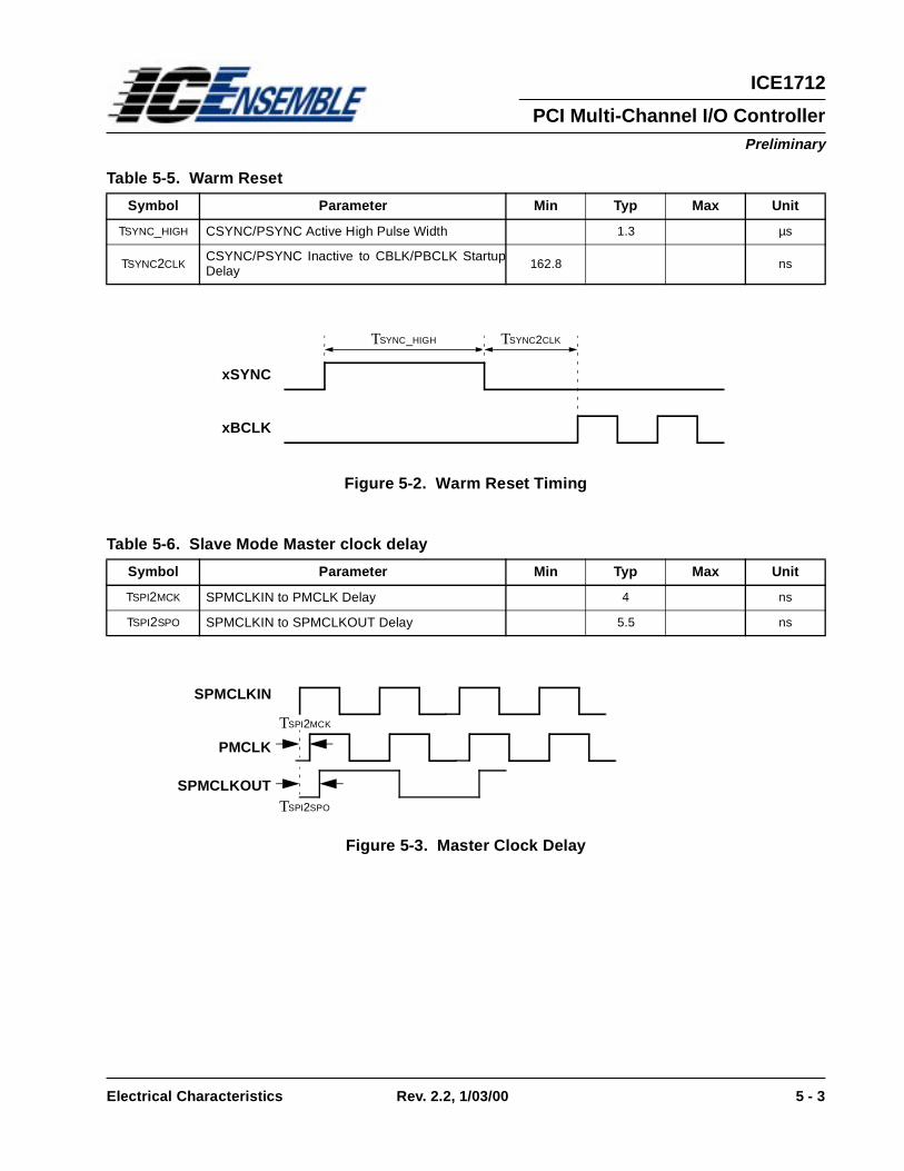
Electrical Characteristics Rev. 2.2, 1/03/00 5 - 3
PCI Multi-Channel I/O Controller
ICE1712
Preliminary
Table 5-5. Warm Reset
Figure 5-2. Warm Reset Timing
Table 5-6. Slave Mode Master clock delay
Figure 5-3. Master Clock Delay
Symbol Parameter Min Typ Max Unit
TSYNC_HIGH CSYNC/PSYNC Active High Pulse Width 1.3 µs
TSYNC2CLKCSYNC/PSYNC Inactive to CBLK/PBCLK StartupDelay 162.8 ns
Symbol Parameter Min Typ Max Unit
TSPI2MCK SPMCLKIN to PMCLK Delay 4 ns
TSPI2SPO SPMCLKIN to SPMCLKOUT Delay 5.5 ns
TSYNC_HIGH TSYNC2CLK
xSYNC
xBCLK
SPMCLKIN
PMCLK
SPMCLKOUT
TSPI2MCK
TSPI2SPO

5 - 4 Rev. 2.2, 1/03/00 Electrical Characteristics
PCI Multi-Channel I/O Controller
ICE1712
Preliminary
Table 5-7. xBCLK / xxSYNC Timing
Figure 5-4. xBCLK to xxSYNC Timing
Symbol Parameter Min Typ Max Unit
xBCLK Frequency see Appendix MHz
TCLK_PERIOD xBCLK Period see Appendix ns
xBCLK Output Jitter TBD 750 ps
TCLK_HIGH xBCLK Pulse Width (high) see Appendix ns
TCLK_LOW xBCLK Pulse Width (low) see Appendix ns
TCLK_DC xBCLK Duty Cycle see Appendix %
xxSYNC Frequency see Appendix kHz
TSYNC_PERIOD xxSYNC Period see Appendix µs
TSYNC_HIGH xxSYNC Pulse Width (high) see Appendix µs
TSYNC_LOW xxSYNC Pulse Width (low) see Appendix µs
TCLK_HIGH TCLK_LOW
xBCLK
TCLK_PERIOD
TSYNC_HIGH TSYNC_LO
xxSYNC
TSYNC_PERIOD

Electrical Characteristics Rev. 2.2, 1/03/00 5 - 5
PCI Multi-Channel I/O Controller
ICE1712
Preliminary
Table 5-8. Setup and Hold
Note: SDATA_IN seup and hold calculations determined by AC’97 controller propagation delay.
Figure 5-5. Setup and Hold Time
Table 5-9. Rise and Fall Time
Symbol Parameter Min Typ Max Unit
TSETUP1 xSDOUT Setup to falling edge of xBCLK 15 ns
THOLD1 xSDOUT Hold from falling edge of xBCLK 5 ns
TSETUP2 xSYNC Setup to rising edge of xBCLK 15 ns
THOLD2 xSYNC Hold to rising edge of xBCLK 5 ns
Symbol Parameter Min Typ Max Unit
TRISE xBCLK rise time 2 6 ns
TFALL xBCLK fall time 2 6 ns
TRISE xxSYNC rise time 2 6 ns
TFALL xxSYNC fall time 2 6 ns
TRISE xSDIN rise time 2 6 ns
TFALL xSDIN fall time 2 6 ns
TRISE xSDOUT rise time 2 6 ns
TFALL xSDOUT fall time 2 6 ns
xBCLK
xSDIN,
xSYNC
xSDOUT
THOLD1TSETUP1
TSETUP2 THOLD2

5 - 6 Rev. 2.2, 1/03/00 Electrical Characteristics
PCI Multi-Channel I/O Controller
ICE1712
Preliminary
Figure 5-6. Rise Time and Fall Time
Table 5-10. AC-link Low Power Mode
Note: CBCLK/PBCLK not to scale.
Figure 5-7. AC-link Power Mode Timing.
Symbol Parameter Min Typ Max Unit
TS2_PDOWNEnd of Slot 2 to CBCLK/PBCLK to CSDIN/PSDINlow
1 µs
TFALLTRISE
BIT_CLK,
SDATA_IN,
SYNC
SDATA_OUT
xBCLK
xSDIN
xSYNC
xSDOUT
TS2_PDOWN
Slot 1 Slot 2

Mechanical Data Rev. 2.2, 1/03/00 6 - 1
PCI Multi-Channel I/O Controller
ICE1712
Preliminary
Section 6: Mechanical Data
6.1 Thermal Specifications
Parameter Min Typ Max Unit
Thermal Resistenace θJA (Still Air) TBD °C/W
Junction Temperature TBD °C

6 - 2 Rev. 2.2, 1/03/00 Mechanical Data
PCI Multi-Channel I/O Controller
ICE1712
Preliminary
6.2 Package Dimensions
Table 6-1. Mechanical Dimensions (millimeters, unless otherwise stated)
Symbol A B C D E F G H I Jminimum 17.0 13.9 23.0 19.9 0°
0.50.17 0.25 – 0.65
maximum 17.4 14.1 23.4 20.1 7° 0.23 - 3.4 0.95
Pin 1 Identifier
D C
H
I
E
J
F G
AB

Appendix Rev. 2.2, 1/03/00 7 - 1
PCI Multi-Channel I/O Controller
ICE1712
Preliminary
Section 7: Appendix
7.1 Appendix AThe following tables will help system designers and software developers correctly set the sampling rate andclock ratios. To determine via software whether AC-link or I²S converters are used, read back PCI61_7. Basedon the outcome either Table 7-1 or 7-2 should be used. To set the sampling rate, regardless of the convertertype used, program MT01. MT02 will have no effect in AC-link mode. MT02 will set I²S interface bpf, over-sampling rate, master clock to sampling rate ratio and similar characteristics. For a visual description of hard-ware settings refer to Figure 4-3 and Figure 4-4 on page 27 and page 28 of chapter 4 respectively .
Note: When using AC’97 codecs, the XIN2 must have 22.5792MHz (512*44.1kHz) to be able to support the samplingrates at 44.1kHz and submultiples. The dividers marked with * at sampling rates 32/16/9.6kHz, will not have 50% dutycycle PMCLK.
Table 7-1. AC-link Interface Parameters and Ratios (when pin 50 floating/pulled up)
PSYNC (SR in kHz) PMCLK/PSYNC XINx/PMCLK PBCLK / PSYNC (bpf)
96 - - -
48 512 1 256
24 512 2 256
12 512 4 256
32 512 1.5* 256
16 512 3* 256
8 512 6 256
9.6 512 5* 256
44.1 512 1 256
22.05 512 2 256
11.025 512 4 256
Table 7-2. I ²S Interface Parameters and Ratios (when pin 50 pulled down)
PSYNC (SR in kHz) PMCLK/PSYNC XINx/PMCLK PBCLK / PSYNC (bpf)
96 128 or 256 2 or 1 64

7 - 2 Rev. 2.2, 1/03/00 Appendix
PCI Multi-Channel I/O Controller
ICE1712
Preliminary
Note: Clock source either 22.5792MHz for 512*44.1kHz or 16.9344MHz for 384*44.1kHz, software controlled viaPCI60_7 and 6. For 512*48kHz, the clock source is 24.576MHz.The divider marked with * like the one at 32kHzsampling rate, will not have 50% duty cycle PMCLK. See MT02 for I²S data format and clock ratios. 48bpf is availablefor XIN2 originating clocks only.
Note: Refer to CS8402A, CS8404A transmitters
Note: Refer to CS8412, CS8414 receivers. To set the controller into slave mode, set MT01_4. When S/PDIF input is themaster clock, 256X is the maximum PMCLK. This input can be used to synchronize with external Super Word Clockinputs. This can also be used to slave multiple PCI controllers in a single workstation.
64 128 3* 64
48 128 or 256 4 or 2 64
24 128 or 256 8 or 4 64
12 128 or 256 16 or 8 64
32 128 or 256 6 or 3* 64
16 128 or 256 12or 6 64
8 128 or 256 24 or 12 64
9.6 128 or 256 20 or 10 64
88.2 128 or 256 2 or 1 64
44.1 256 or 384 2 or 1 64 or 48
22.05 256 or 384 4 or 2 64 or 48
11.025 256 or 384 8 or 4 64 or 48
Table 7-3. S/PDIF Output I ²S Interface Parameters and Ratios
SPSYNC (SR in kHz) SPMCLKOUT/SPSYNC SPSCLK/SPSYNC (bpf)
96 128 64
48 128 64
44.1 128 64
32 128 64
Table 7-4. S/PDIF Input I ²S Interface Parameters and Ratios
SPSYNC (SR in kHz) SPMCLKIN/SPSYNC SPSCLK/SPSYNC (bpf)
96 256 64
48 256 64
44.1 256 64
32 256 64
Table 7-2. I ²S Interface Parameters and Ratios (when pin 50 pulled down)
PSYNC (SR in kHz) PMCLK/PSYNC XINx/PMCLK PBCLK / PSYNC (bpf)