partitioning signal processing applications to different ... · partitioning signal processing...
TRANSCRIPT

Partitioning Signal Processing Applications to Different Granularity Reconfigurable Logic
MICHALIS D. GALANIS1, GREGORY DIMITROULAKOS2, ATHANASSIOS P. KAKAROUNTAS3, COSTAS E. GOUTIS4
VLSI Design Laboratory, Electrical & Computer Engineering Department University of Patras, Rio Campus, GREECE
Abstract: - In this paper, we propose a methodology for partitioning DSP applications between the fine and coarse-grain reconfigurable hardware for improving performance. The fine-grain logic is implemented by an embedded FPGA unit, while for the coarse-grain reconfigurable hardware, a 2-Dimensional array of Processing Elements is considered. These different granularity reconfigurable functional units are embedded in a hybrid platform. The proposed methodology mainly consists of three steps, the analysis, the mapping onto the coarse-grain reconfigurable array, and the mapping onto the fine-grain reconfigurable hardware. The experiments for five real-world applications show that the speedup, relative to an all-FPGA solution, ranges from 1.4 to 3.1 for the considered applications. Key-Words: - DSP, Hybrid reconfigurable architectures, Partitioning, Coarse-grain reconfigurable hardware, FPGA, Scheduling. 1 Introduction Hybrid granularity reconfigurable systems [1], [2], [3] offer extra advantages in terms of performance, power dissipation and great flexibility, as well, to efficiently implement DSP and multimedia applications. Hybrid architectures usually consist of fine-grain reconfigurable units, typically implemented in Field Programmable Gate Array (FPGA) technology, coarse-grain reconfigurable units implemented in ASIC technology, microprocessor(s), data and instruction memories. Certain parts of the application are better suited to be executed on the coarse-grain units and other parts on the fine-grain units, due to the special characteristics of the heterogeneous reconfigurable units included in the platform. The fine-grain reconfigurable hardware’s granularity is typically four or five bits. It can efficiently execute small bit-width operations, like bit-level ones, and Finite State Machine (control) structures. Coarse-grain reconfigurable hardware has been proposed for accelerating loops of multimedia and DSP applications in embedded systems. It consists of a large number of Processing Elements (PEs) connected with a reconfigurable interconnect network. This work considers coarse-grain architectures where the PEs are organized in a 2-Dimensional (2D) array and they are connected with mesh-like reconfigurable networks [1], [4], [5], [6]. In this paper, these architectures are called Coarse-
Grain Reconfigurable Arrays (CGRAs). This subset of coarse-grain reconfigurable logic has become popular in both academia [4], [5] and in industry [6], [7].
An automated partitioning method between the fine and coarse-grain reconfigurable hardware parts of an embedded hybrid reconfigurable platform is introduced in this work. Critical parts, called kernels, are accelerated by executing them on the coarse-grain reconfigurable hardware. It has been shown that performance is improved when application’s segments, which contribute to the majority of the execution time, are speeded-up [8]. The main parts of the method are the analysis process for detecting kernels in the application’s code that is to be mapped to the Reconfigurable Functional Units (RFUs) of the hybrid platform, and the mapping procedures to the fine and coarse-grain reconfigurable logic. The proposed method is evaluated in this paper using five real-life applications. An average speedup of 2.3 relative to an all-FPGA solution is achieved for the considered experimentation.
The rest of the paper is organized as follows: The related work is presented in section 2, while section 3 gives an overview of the proposed partitioning method. Section 4 describes the analysis process. Section 5 presents the CGRA architecture template and the mapping algorithm to it. The mapping algorithm for FPGAs is given in section 6. Section 7
Proceedings of the 5th WSEAS Int. Conf. on SIGNAL, SPEECH and IMAGE PROCESSING, Corfu, Greece, August 17-19, 2005 (pp143-148)
presents the experimental results and section 8 concludes this paper.
2 Related work The Strategically Programmable System [2] is a reconfigurable System-on-Chip (SoC) architecture that combines fine-grain reconfigurable units and ASIC coarse-grain modules which are pre-placed within a fully reconfigurable fabric. Chameleon heterogeneous SoC architecture [3] contains a processor, an FPGA unit and a coarse-grain reconfigurable part. The latter part is composed by reconfigurable processor tiles, called MONTIUM. The hybrid granularity approach has been recently adopted in current FPGA devices, like the Xilinx Virtex-II/4 [9] and Altera Stratix [10]. These devices contain coarse-grain components which are ASIC multiplier units operating on 18-bits operands.
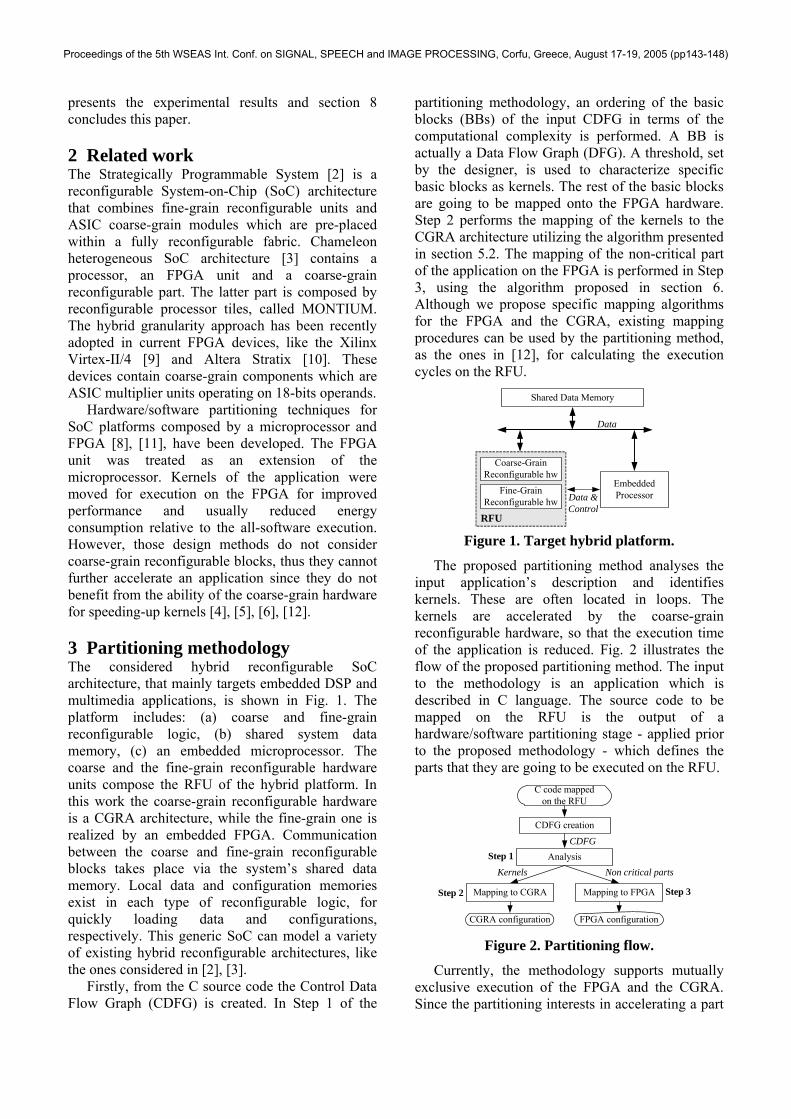
Hardware/software partitioning techniques for SoC platforms composed by a microprocessor and FPGA [8], [11], have been developed. The FPGA unit was treated as an extension of the microprocessor. Kernels of the application were moved for execution on the FPGA for improved performance and usually reduced energy consumption relative to the all-software execution. However, those design methods do not consider coarse-grain reconfigurable blocks, thus they cannot further accelerate an application since they do not benefit from the ability of the coarse-grain hardware for speeding-up kernels [4], [5], [6], [12]. 3 Partitioning methodology The considered hybrid reconfigurable SoC architecture, that mainly targets embedded DSP and multimedia applications, is shown in Fig. 1. The platform includes: (a) coarse and fine-grain reconfigurable logic, (b) shared system data memory, (c) an embedded microprocessor. The coarse and the fine-grain reconfigurable hardware units compose the RFU of the hybrid platform. In this work the coarse-grain reconfigurable hardware is a CGRA architecture, while the fine-grain one is realized by an embedded FPGA. Communication between the coarse and fine-grain reconfigurable blocks takes place via the system’s shared data memory. Local data and configuration memories exist in each type of reconfigurable logic, for quickly loading data and configurations, respectively. This generic SoC can model a variety of existing hybrid reconfigurable architectures, like the ones considered in [2], [3].
Firstly, from the C source code the Control Data Flow Graph (CDFG) is created. In Step 1 of the
partitioning methodology, an ordering of the basic blocks (BBs) of the input CDFG in terms of the computational complexity is performed. A BB is actually a Data Flow Graph (DFG). A threshold, set by the designer, is used to characterize specific basic blocks as kernels. The rest of the basic blocks are going to be mapped onto the FPGA hardware. Step 2 performs the mapping of the kernels to the CGRA architecture utilizing the algorithm presented in section 5.2. The mapping of the non-critical part of the application on the FPGA is performed in Step 3, using the algorithm proposed in section 6. Although we propose specific mapping algorithms for the FPGA and the CGRA, existing mapping procedures can be used by the partitioning method, as the ones in [12], for calculating the execution cycles on the RFU.
Embedded Processor
Shared Data Memory
Data
Data &Control
Coarse-Grain Reconfigurable hw
RFU
Fine-Grain Reconfigurable hw
Figure 1. Target hybrid platform.
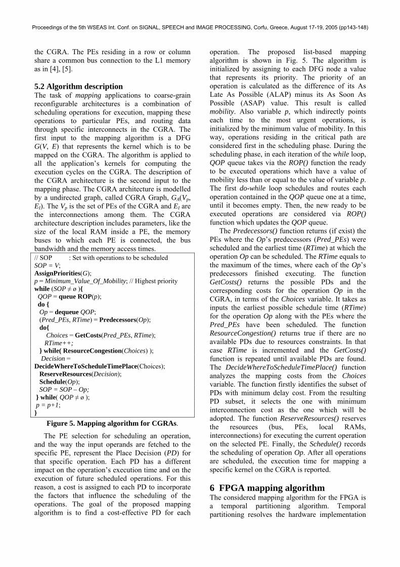
The proposed partitioning method analyses the input application’s description and identifies kernels. These are often located in loops. The kernels are accelerated by the coarse-grain reconfigurable hardware, so that the execution time of the application is reduced. Fig. 2 illustrates the flow of the proposed partitioning method. The input to the methodology is an application which is described in C language. The source code to be mapped on the RFU is the output of a hardware/software partitioning stage - applied prior to the proposed methodology - which defines the parts that they are going to be executed on the RFU.
C code mapped on the RFU
CDFG creation
Analysis
Mapping to CGRA Mapping to FPGA
FPGA configuration
CDFG
Non critical partsKernels
Step 1
Step 2 Step 3
CGRA configuration
Figure 2. Partitioning flow.
Currently, the methodology supports mutually exclusive execution of the FPGA and the CGRA. Since the partitioning interests in accelerating a part
Proceedings of the 5th WSEAS Int. Conf. on SIGNAL, SPEECH and IMAGE PROCESSING, Corfu, Greece, August 17-19, 2005 (pp143-148)

of a sequential software program, which is often the case in implementing embedded applications in a high-level language, the performance gains from concurrent execution of the CGRA and the FPGA could be likely small. The parallel execution on the FPGA and on the CGRA is a topic of our future research activities. The total execution time of the application’s part mapped on the RFU of Fig. 1, after the partitioning, is:
ttotal = tFPGA + tCGRA + tcomm (1) where tFPGA is the execution time of the non-critical part on the FPGA hardware, tCGRA is the execution time on the CGRA and tcomm is the time required for transferring data between the two types of reconfigurable hardware. The tFPGA and the tCGRA include the reconfiguration time of the FPGA and the CGRA, respectively.
4 Analysis process The analysis procedure of the partitioning method outputs the kernel and non-critical segments of the application’s part which is to be mapped on the RFU of the hybrid SoC. The inherent computational complexity of each basic block in the input CDFG is a reasonable criterion to detect kernels. This information is obtained through a combination of profiling and static analysis within basic blocks. Fig. 3 shows the analysis diagram.
CDFG
Basic Block Dynamic Analysis
Execution frequencies
Basic Block Static Analysis
Weighted sum in BBs
X
Total weights of BBs
Application’sinputs
BB ordering & selection
Non critical BBsKernels
Threshold
Figure 3. Analysis flow.
We have used the MachineSUIF compiler [13] for performing profiling at the basic block level. The profiling is performed with application’s representative inputs. The profiling step reports the execution frequency of the basic blocks. For the static analysis, a MachineSUIF compiler pass has been developed that identifies the type of operations inside each basic block. Afterwards, this pass calculates the weighted sum of the operations composing a specific basic block. The weight of an operation, e.g. a multiplication one, is related to the delay typically required for the execution of this operation. For example, a multiplication operation is assigned with a larger weight that an ALU one. The
total weight of a basic block, representing its computational complexity, is computed as the product of the basic block’s execution frequency times the weight of the operations of this basic block. After the total weight calculation, an ordering of the basic blocks is performed. We consider kernels, the BBs which have a weight over a user-defined threshold. We mention that kernels are considered those BBs that they are composed by word-level operations (like 16-bit multiplications) which are efficiently implemented on the CGRA. 5 CGRA mapping algorithm 5.1 CGRA architecture template The considered generic CGRA template is based on characteristics found in the majority of the 2D coarse-grain reconfigurable architectures [1], [4], [5], and it can be used as a realistic model for mapping applications to such type of architectures. The proposed architecture template is shown in Fig. 4a. Each PE is connected to its nearest neighbours, while there are cases [5], [7] where there are also direct connections among all the PEs across a column and a row. A PE usually contains one Functional Unit (FU), which it can be configured to perform a specific word-level operation each time. Typical operations supported by the FU are ALU, multiplication, and shifts. For storing intermediate values between computations and data fetched from memory, a local RAM exists inside a PE. Fig. 4b shows an example of a PE architecture.
Configuration memory
Main data memory
Scratch Pad Mem
ory
PE
(a) (b)
s
In1 In 2
OutFU
register
out1 out 2RAM
in
Reconfiguration registercontrol
Mem
ory
BuFr
om P
Es
..
control
Figure 4. (a) CGRA generic architecture, (b) PE architecture.
The configuration memory of the CGRA (Fig. 4a) stores the whole configuration for setting up the CGRA for the execution of kernels of an application. Configuration caches distributed in the CGRA and reconfiguration registers inside the PEs are used for the fast reconfiguration of the CGRA. The hierarchy of the data memory consists of: (a) the zero memory level, called L0, which is formed by the local RAMs inside the PEs, (b) the L1 which is a scratch-pad memory, and (c) the main data memory of the CGRA which is a part of the system’s data memory (Fig. 1). The L1 serves as a local memory for quickly loading data in the PEs of
Proceedings of the 5th WSEAS Int. Conf. on SIGNAL, SPEECH and IMAGE PROCESSING, Corfu, Greece, August 17-19, 2005 (pp143-148)
the CGRA. The PEs residing in a row or column share a common bus connection to the L1 memory as in [4], [5]. 5.2 Algorithm description The task of mapping applications to coarse-grain reconfigurable architectures is a combination of scheduling operations for execution, mapping these operations to particular PEs, and routing data through specific interconnects in the CGRA. The first input to the mapping algorithm is a DFG G(V, E) that represents the kernel which is to be mapped on the CGRA. The algorithm is applied to all the application’s kernels for computing the execution cycles on the CGRA. The description of the CGRA architecture is the second input to the mapping phase. The CGRA architecture is modelled by a undirected graph, called CGRA Graph, GA(Vp, EI). The Vp is the set of PEs of the CGRA and EI are the interconnections among them. The CGRA architecture description includes parameters, like the size of the local RAM inside a PE, the memory buses to which each PE is connected, the bus bandwidth and the memory access times. // SOP : Set with operations to be scheduled SOP = V; AssignPriorities(G); p = Minimum_Value_Of_Mobility; // Highest priority while (SOP ≠ ø ){ QOP = queue ROP(p); do { Op = dequeue QOP; (Pred_PEs, RTime) = Predecessors(Op); do{ Choices = GetCosts(Pred_PEs, RTime); RTime++; } while( ResourceCongestion(Choices) ); Decision = DecideWhereToScheduleTimePlace(Choices); ReserveResources(Decision); Schedule(Op); SOP = SOP – Op; } while( QOP ≠ ø ); p = p+1; }
Figure 5. Mapping algorithm for CGRAs.
The PE selection for scheduling an operation, and the way the input operands are fetched to the specific PE, represent the Place Decision (PD) for that specific operation. Each PD has a different impact on the operation’s execution time and on the execution of future scheduled operations. For this reason, a cost is assigned to each PD to incorporate the factors that influence the scheduling of the operations. The goal of the proposed mapping algorithm is to find a cost-effective PD for each
operation. The proposed list-based mapping algorithm is shown in Fig. 5. The algorithm is initialized by assigning to each DFG node a value that represents its priority. The priority of an operation is calculated as the difference of its As Late As Possible (ALAP) minus its As Soon As Possible (ASAP) value. This result is called mobility. Also variable p, which indirectly points each time to the most urgent operations, is initialized by the minimum value of mobility. In this way, operations residing in the critical path are considered first in the scheduling phase. During the scheduling phase, in each iteration of the while loop, QOP queue takes via the ROP() function the ready to be executed operations which have a value of mobility less than or equal to the value of variable p. The first do-while loop schedules and routes each operation contained in the QOP queue one at a time, until it becomes empty. Then, the new ready to be executed operations are considered via ROP() function which updates the QOP queue.
The Predecessors() function returns (if exist) the PEs where the Op’s predecessors (Pred_PEs) were scheduled and the earliest time (RTime) at which the operation Op can be scheduled. The RTime equals to the maximum of the times, where each of the Op’s predecessors finished executing. The function GetCosts() returns the possible PDs and the corresponding costs for the operation Op in the CGRA, in terms of the Choices variable. It takes as inputs the earliest possible schedule time (RTime) for the operation Op along with the PEs where the Pred_PEs have been scheduled. The function ResourceCongestion() returns true if there are no available PDs due to resources constraints. In that case RTime is incremented and the GetCosts() function is repeated until available PDs are found. The DecideWhereToScheduleTimePlace() function analyzes the mapping costs from the Choices variable. The function firstly identifies the subset of PDs with minimum delay cost. From the resulting PD subset, it selects the one with minimum interconnection cost as the one which will be adopted. The function ReserveResources() reserves the resources (bus, PEs, local RAMs, interconnections) for executing the current operation on the selected PE. Finally, the Schedule() records the scheduling of operation Op. After all operations are scheduled, the execution time for mapping a specific kernel on the CGRA is reported.
6 FPGA mapping algorithm The considered mapping algorithm for the FPGA is a temporal partitioning algorithm. Temporal partitioning resolves the hardware implementation
Proceedings of the 5th WSEAS Int. Conf. on SIGNAL, SPEECH and IMAGE PROCESSING, Corfu, Greece, August 17-19, 2005 (pp143-148)
of an application that does not fit into the FPGA hardware by time-sharing of the device in a way that each partition fits in the available hardware resources, i.e. the CLBs of an FPGA. Then, the partitioned solution is executed by time-sharing the device such that the initial functionality is maintained. The mapping algorithm handles CDFGs, by iteratively mapping the DFGs composing the CDFG. The proposed algorithm classifies the operations (nodes) of the DFG, of a non-critical application’s basic block, according to their ASAP levels. The approach followed is that the nodes are executed in increasing order relative to their ASAP levels. This ensures stable inputs for every DFG node at the next level. i = 1; level = 1; area_covered = 0; while (lev ≤ maximum_level) { for (each node ui with level(ui)= lev) { current_area = size(ui); if (area_covered + current_area ≤ AFPGA) { partition(ui) = i; area_covered = area_covered + current_area; } else { i = i + 1; partition(ui) = i; area_covered = current_area; } level = level + 1; } } Figure 6. FPGA temporal partitioning algorithm.
The pseudocode of the proposed temporal partitioning algorithm is illustrated in Fig. 6. In this pseudocode, partition(ui) denotes the temporal partition to which the node ui belongs (1 iu N≤ ≤ , N is the number of DFG nodes) and maximum_level denotes the maximum level of any DFG node. The algorithm traverses each node of the DFG, level by level, and assigns them to a partition. The DFG nodes are assigned to partitions numbered 1 and beyond. All the nodes from level 1 to maximum_level are traversed. Nodes of the same ASAP level are placed in a single partition and if the available area in the FPGA hardware is exhausted, then the nodes are assigned to the next partition. If the nodes in the current ASAP level are all assigned to a partition, then the next level nodes are considered. Initially, a partition has no nodes. The AFPGA is the area available for mapping the DFG operations on the FPGA. The AFPGA parameter does not include the area needed for the routing resources (like switch boxes) in an FPGA device. The size(ui),
which is the area occupied by the mapped DFG node, and the AFPGA are parameters dependent from the fine-grain reconfigurable technology. Since these are parameters in our algorithm, the algorithm is applicable to every type of fine-grain reconfigurable hardware.
Data memories are used for storing the input and output values among the temporal partitions. For example, local data memories embedded in the FPGA, as in [9], [10], can be used. According to the application’s data and control-flow, the appropriate partition is executed on the FPGA. For each temporal partition, full reconfiguration of the FPGA hardware is performed. The reconfiguration time has the same value for each partition of a DFG mapped to FPGA. 7 Experimental results The proposed methodology has been automated by developing in C++ a prototype software framework. This framework is used for calculating the execution times when the partitioning on the RFU of the hybrid platform takes place. We have used the following five real-life applications, written in C language: (a) a medical imaging application called cavity detector, (b) an IEEE 802.11a baseband OFDM transmitter, (c) a wavelet-based image-compressor, (d) a video compression scheme, called Quadtree Structured Difference Pulse Code Modulation (QSDPCM), and (e) a still-image JPEG encoder.
The RFU’s clock period is set to the clock period of the FPGA. Typical clock frequencies are assumed for the FPGA and the CGRA. The FPGA is clocked at 100 MHz, while the CGRA at 200MHz. These two clock frequencies remain constant for all the applications partitioned on the RFU. The area of the FPGA equals 5000 units, i.e. AFPGA=5000, which approximately corresponds to the number of CLBs in a Xilinx XC2V1000 device [9]. We consider two different CGRA architectures for accelerating kernels. The first architecture is a 2D CGRA of 16 PEs connected in a 4x4 array (CGRA1). The second one is a 2D CGRA of 36 PEs connected in a 6x6 array (CGRA2). In both cases of CGRA architectures, the PEs are directly connected to all other PEs in the same row and same column through vertical and horizontal interconnections, as in a quadrant of MorphoSys [5]. There is one 16-bit FU, in each PE that can execute any operation in one CGRA’s clock cycle. Two buses per row are dedicated for transferring data to the PEs from the scratch-pad (L1) memory. The delay of fetching one word from the local scratch-pad memory is one CGRA’s cycle.
Proceedings of the 5th WSEAS Int. Conf. on SIGNAL, SPEECH and IMAGE PROCESSING, Corfu, Greece, August 17-19, 2005 (pp143-148)

We assume that the full reconfiguration of the FPGA device endures 5 cycles. This reconfiguration time is achievable with reconfiguration caches and proper developed mechanisms, as in the case of the Garp architecture [11]. On the other hand, we assume that the CGRA configuration caches (for both CGRA1 and CGRA2 architectures) are sufficiently large to store the configurations of the kernels. In this case, cycle-by-cycle reconfiguration of the CGRA is supported.
In the analysis, we give a weight equal to 1 for the ALU operations and a weight equal to 2 for the multiplication ones. The threshold for identifying kernels was set to the half of the maximum total weight, i.e. equal to the half of the weight of the most critical BB in each application. After performing the analysis procedure, it was found that the parts of the five applications selected for mapping on the RFU are composed by a small number of kernels, at most equal to 4.
Table 1. Execution cycles and speedups
Application CGRA arch.
Initial Cycles
Final Cycles Speedup
4x4 31,514 2.7 OFDM trans. 6x6 85,824 30,500 2.8
4x4 6,870,480 3.1 Cavity 6x6 21,090,224 6,800,234 3.1 4x4 3,608,556 2.4 Compressor 6x6 8,586,732 3,522,540 2.4 4x4 11,792,682 2.0 QSDPCM 6x6 24,157,386 11,520,234 2.1 4x4 6,807,008 1.4 JPEG enc. 6x6 9,274,408 6,798,816 1.4
Average: 2.3 The third column of Table 1 reports the RFU
clock cycles (Initial_Cycles) for the execution of the applications’ parts on the FPGA without accelerating the kernels on the CGRA. These cycles include the reconfiguration time of the FPGA. The kernels of the five applications were mapped on the 4x4 and on the 6x6 CGRA architectures (CGRA arch.). For each application, the number of RFU’s clock cycles resulting after the partitioning and the acceleration with the CGRA1 and CGRA2 architectures is presented in the fourth column of Table 1 (Final_Cycles).
It is deduced from Table 1 that the performance improvements relative to the all-FPGA execution (Initial_Cycles) are significant. These improvements are slightly larger for the 6x6 architecture (CGRA2) due to the larger number of PEs that better exploit operation parallelism in the applications than the 4x4 array (CGRA1). The speedup, which is defined as the Initial_Cycles/Final_Cycles ratio, ranges from 1.4 to 3.1, with an average value of 2.3.
8 Conclusions An automated partitioning flow for speeding-up applications’ parts mapped on the RFU logic of a hybrid SoC by executing kernels on coarse-grain reconfigurable hardware was presented. Significant speedups, ranging from 1.4 to 3.1, were reported. Acknowledgements
This research has been partly funded by the Alexander S. Onassis Public Benefit Foundation. References: [1] R. Hartenstein, “A Decade of Reconfigurable
Computing: A Visionary Retrospective”, in Proc. of DATE, pp. 642-649, 2001.
[2] R. Kastner et al., “Instruction Generation for Hybrid Reconfigurable Systems”, in ACM TODAES, vol. 7, no.4, pp. 605-627, October 2002.
[3] G. K. Rauwerda et al., “Mapping Wireless Communication Algorithms onto a Reconfigurable Architecture”, in the Journal of Supercomputing, Springer, vol. 30, no. 3, pp. 263-282, Dec. 2004.
[4] T. Miyamori and K. Olukutun, “REMARC: Reconfigurable Multimedia Array Coprocessor”, in IEICE Trans. On Information and Systems, pp. 389-397, 1999.
[5] H. Singh et al., “MorphoSys: An Integrated Reconfigurable System for Data-Parallel and Communication-Intensive Applications”, in IEEE Trans. on Computers, vol. 49, no. 5, pp. 465-481, May 2000.
[6] V. Baumgarte et al., “PACT XPP-A Self-Reconfigurable Data Processing Architecture”, in the Journal of Supercomputing, vol. 26, no. 2, pp. 167-184, September 2003.
[7] Morpho Tech., www.morphotech.com, 2005.sss [8] G. Stitt et al., “Energy Savings and Speedups
from Partitioning Critical Software Loops to Hardware in Embedded Systems”, in ACM TECS, vol. 3, no. 1, pp. 218-232, Feb. 2004.
[9] Virtex FPGAs, www.xilinx.com, 2005. [10] Altera FPGAs, www.altera.com, 2005. [11] T.J. Callahan et al., “The Garp Architecture and
C Compiler”, in IEEE Computer, vol. 33, no. 4, pp. 62-69, April 2000.
[12] B. Mei et al., “Exploiting Loop-Level Parallelism on Coarse-grained Reconfigurable Architectures Using Modulo Scheduling”, in Proc. of DATE ’03, pp. 255-261, 2003.
[13] MachineSUIF, http://www.eecs.harvard.edu/hube/research/machsuif.html, 2005.
Proceedings of the 5th WSEAS Int. Conf. on SIGNAL, SPEECH and IMAGE PROCESSING, Corfu, Greece, August 17-19, 2005 (pp143-148)