paper view article online view journal | view issue · make semiconductor nanocrystals (ncs)...
TRANSCRIPT
Nanoscale
PAPER
Cite this: Nanoscale, 2017, 9, 4730
Received 19th November 2016,Accepted 3rd March 2017
DOI: 10.1039/c6nr09021d
rsc.li/nanoscale
Band-edge oscillator strength of colloidalCdSe/CdS dot-in-rods: comparison of absorptionand time-resolved fluorescence spectroscopy†
I. Angeloni,a,b W. Raja,‡a,c A. Polovitsyn,a,c F. De Donato,a R. Proietti Zaccaria*a andI. Moreels *a
We studied the oscillator strength fgap of the band gap transition in heteronanocrystals (hNCs) with a
spherical CdSe core embedded in an elongated CdS shell. A comparison with fgap of core-only CdSe NCs
confirmed a reduction of the electron–hole overlap in hNCs with a band gap larger than 2.05 eV or
smaller than 1.98 eV. However, the decrease in fgap is limited to about 50% when compared to CdSe NCs,
suggesting that residual confinement still localizes the electron near the core. We correlated fgap with the
radiative lifetime obtained from multiexponential photoluminescence (PL) decay traces. The different
components were attributed to radiative decay, or deep and shallow carrier trapping, respectively, using
the PL quantum efficiency (QE) as a guideline. Our data highlight the challenges associated when extract-
ing the radiative decay, and demonstrate the added value of absorption spectroscopy to obtain the band-
edge oscillator strength and the associated radiative recombination rate in colloidal hNCs.
Introduction
Narrow emission linewidths over a wide spectral range,together with the possibility to fine-tune their optical pro-perties via size, shape and composition are key qualities thatmake semiconductor nanocrystals (NCs) frontier materials foroptoelectronic applications, along with the versatility and low-cost nature of the colloidal synthesis routes employed toproduce them. In the last few years several procedures havebeen developed to encapsulate the core into a shell made of asecond semiconductor.1–4 The obtained hetero-structure NCs(hNCs) multiply the possibilities to control the optical pro-perties, via the engineering of the conduction band (CB) andvalence band (VB) alignment of core and shell. It is thuspossible to obtain structures in which electrons and holes are
both confined to the same region, as in the case of type ICdSe/ZnS1 core/shell NCs, or in which electrons and holes areconfined to different materials, as in type II ZnSe/CdS,2,5
CdTe/CdSe,3 or CdSe/ZnTe4 NCs. CdSe/CdS NCs form aparticular case. Because of the small offset in the CB of thetwo materials, the hole is localized in the core while the elec-tron delocalizes into the CdS shell and remains bound to thehole via Coulomb interactions. For this reason, CdSe/CdShNCs are usually referred to as quasi-type-II structures, andthey are among the most studied hNCs to date.
The actual degree of delocalization still varies betweendifferent reports. Optical measurements and theoretical calcu-lations6,7 have suggested that the electron can strongly deloca-lize along the CdS rod length, while scanning tunneling spec-troscopy (STS) experiments have supported a type-I band offsetwith electrons and holes both confined to the CdSe core.8
More recent work suggested that the core diameter plays a dis-tinctive role in the electron delocalization, as CdSe/CdS hNCsshowed a transition from a type-I to a quasi-type-II regimewhen the core becomes sufficiently small.9–11 Processing hNCsinto thin films may also affect the optical properties, asCdSe/CdS dot-in-rod (DiR) aerogels showed an increase of theelectron delocalization due to DiR coupling.12
Measurements of the photoluminescence (PL) lifetime haveoften been used to support the quasi-type-II behavior ofCdSe/CdS hNCs. Although in principle straightforward, the cor-relation of the electron–hole overlap with lifetime depends onseveral factors. Most importantly, the influence of nonradiative
†Electronic supplementary information (ESI) available: Details of the materialproperties, finite element simulations, calculations of the oscillator strength,comparison of the oscillator strength with literature, dependence of the oscil-lator strength on DiR geometry, details on the estimation of the CdS band gap,and lifetime analysis. See DOI: 10.1039/c6nr09021d‡Current address: Nanooptische Konzepte für die PV, Helmholtz-ZentrumBerlin, H.-Meitner-Platz 1, 14109, Germany.
aIstituto Italiano di Tecnologia, via Morego 30, 16163 Genova, Italy.
E-mail: [email protected], [email protected] di Chimica e Chimica Industriale, Università di Genova,
Via Dodecaneso 33, 16146 Genova, ItalycDipartimento di Fisica, Università di Genova, Via Dodecaneso 33, 16146 Genova,
Italy
4730 | Nanoscale, 2017, 9, 4730–4738 This journal is © The Royal Society of Chemistry 2017
Ope
n A
cces
s A
rtic
le. P
ublis
hed
on 0
6 M
arch
201
7. D
ownl
oade
d on
12/
09/2
017
13:5
8:05
. T
his
artic
le is
lice
nsed
und
er a
Cre
ativ
e C
omm
ons
Attr
ibut
ion-
Non
Com
mer
cial
3.0
Unp
orte
d L
icen
ce.
View Article OnlineView Journal | View Issue

recombination that competes with the radiative relaxationchannel must be taken into account, often accomplished viadetermination of the NC PL quantum efficiency (QE).
In this work we studied the band edge optical properties ofwurtzite CdSe NCs and CdSe/CdS DiRs using optical absorp-tion spectroscopy which, through the absorption cross section,allows us to access the band-edge oscillator strength, an intrin-sic material property. Finite element simulations were per-formed to obtain the electric field profile inside the CdSe core,considering the non-analytical shape of the hNC – i.e.,a spherical core located at one side of a rod-shaped shell – andthe presence of an organic ligand shell. The resulting bandedge oscillator strength fgap reveals a reduced electron–holeoverlap only for DiRs with either a small (diameter smallerthan about 3.5 nm) or a large (diameter larger than about4.5 nm) CdSe core. The data are then compared to time-resolved PL spectroscopy, which allows us to reassess the roleof the PL QE in determining the radiative recombinationdynamics. As for the absorption measurements, both DiRswith a core diameter below 3.5 nm and above 4.5 nm show areduced electron–hole overlap.
ExperimentalMaterials
Trioctylphosphine oxide (TOPO, 99%), trioctylphosphine (TOP,97%), cadmium oxide (CdO, 99.999%), sulfur powder (99%),and selenium powder (99.99%) were purchased from StremChemicals. Cadmium oxide (CdO, 99.5%) was purchased fromSigma-Aldrich. Octadecylphosphonic acid (ODPA, 99%) andhexylphosphonic acid (HPA, 99%) were purchased fromPolycarbon Industries.
Synthesis
To synthesize CdSe cores (QD1 to QD5 shown in Table S2†),TOPO (3 g), ODPA (0.280 mg), and CdO (0.060 g, StremChemicals) were mixed in a 25 mL three-necked flask andheated to ca. 120 °C for 1 hour.7 Then, under a nitrogen atmo-sphere, the solution was heated to 380 °C to completely dis-solve the CdO. When the solution became colorless, 1.5 mL ofTOP was injected and the temperature was allowed to recoverto 380 °C. Se:TOP (0.058 g Se dissolved in 0.500 g TOP) wasinjected at 380 °C and the growth time was varied to obtaindifferent sizes of CdSe NCs. After synthesis, the NCs werepurified three times by precipitation and re-dispersion, usingtoluene as a solvent and methanol as a non-solvent. Thesample was finally dispersed in 3 mL of toluene.
A second set of CdSe cores (QD6 to QD14 in Table S2†) wassynthesized by mixing TOPO (3.0 g), ODPA (0.280 g) and CdO(0.060 g, Sigma-Aldrich) in a 50 mL flask. The mixture washeated to ca. 150 °C under vacuum for about 1 hour. Then,under a nitrogen atmosphere, the solution was heated toabove 300 °C to dissolve the CdO until it turned optically clear.Next, 1.5 g of TOP was injected into the flask and the tempera-ture was allowed to recover to 370 °C for the injection of the
Se:TOP solution (0.058 g Se with 0.360 g TOP). The reactiontime was modified in order to synthesize CdSe NCs of differentsizes. After the synthesis, the NCs were purified as describedabove. Both types of CdSe cores were used as seeds in the syn-thesis of CdSe/CdS DiRs, according to the procedure ofCarbone et al.7
Characterization
Transmission electron microscopy (TEM) images were col-lected by drop casting a dilute suspension of NCs on acarbon coated 200 mesh copper grid and imaging them with aJEOL JEM 1011 TEM equipped with a thermo-ionic source(tungsten filament) operating at 100 kV. The diameter of theCdSe cores was calculated using the calibration curve proposedby Jasieniak et al.,13 while the dimensions of the CdSe/CdSDiRs were estimated from TEM images using about100–200 NCs.
UV-Vis absorption spectra were obtained with a Varian Cary300 UV-vis spectrophotometer. Photoluminescence measure-ments were performed with an Edinburgh Instruments FLS920spectrofluorometer. Samples were dispersed in chloroformand excited by using a xenon lamp coupled with a mono-chromator set at 530 nm (10 nm bandwidth). PL decay traceswere collected in time-correlated single photon mode. Sampleswere excited with a 50 ps, 405 nm pulsed laser, and the PLdecay was measured in a region of typically 10 nm around theemission maximum. A pulse period of 2 μs was chosen toensure full decay between the pulses. The traces were fittedusing a sum of three exponential functions. For each sample,we analysed the three time constants resulting from the fit torelate them to radiative processes, hole trapping in mid-gapstates14 or delayed emission.15 Finally an area-weighted averagelifetime τavg was calculated including only the componentswhich were considered to constitute the radiative decay.
The PL QE was measured using an integrating sphere.Samples were excited at 530 nm with a xenon lamp, and theoptical density at the excitation wavelength was adjusted to 0.1or lower. The accuracy of the system was verified using a solu-tion of Rhodamine 101 in ethanol.16 The obtained QE value of94% ± 7% is in close agreement with literature values.17 Toanalyse the relation between QE and radiative lifetime, forthree representative samples additional PL QE measurementswere performed with an excitation wavelength of 405 nm (thetypical wavelength used for PL decay measurements), and inaddition the PL decay was collected with a 510 nm pulsedlaser (close to that of the 530 nm used in the QEmeasurements).
Finite element simulations
In the case of non-analytical shapes such as our CdSe/CdSDiRs that are composed of a CdSe core located near one end ofan elongated CdS shell, numerical models are required toevaluate the dielectric screening.18 We performed 3D finiteelement numerical simulations (COMSOL multiphysics) toexamine the near field optical properties of hNCs and calculatethe electric field inside the CdSe core. The simulation domain
Nanoscale Paper
This journal is © The Royal Society of Chemistry 2017 Nanoscale, 2017, 9, 4730–4738 | 4731
Ope
n A
cces
s A
rtic
le. P
ublis
hed
on 0
6 M
arch
201
7. D
ownl
oade
d on
12/
09/2
017
13:5
8:05
. T
his
artic
le is
lice
nsed
und
er a
Cre
ativ
e C
omm
ons
Attr
ibut
ion-
Non
Com
mer
cial
3.0
Unp
orte
d L
icen
ce.
View Article Online
comprised a spherical volume representing a CdSe/CdS DiRembedded in chloroform. The refractive index of chloroformwas taken from Samoc.19 We used a plane wave as externalexcitation, hence allowing for the employment of the scatteredfield formulation, where only the scattered solution needs tobe computed. The wavelength λ = 610 nm has been chosen asa typical value for the first excitonic transition of our dataset.Perfectly matched layer (PML) boundary conditions were usedto avoid undesired reflections. Based on the polarisation of theincident external electric field (Eext = 1 V m−1), either parallelor perpendicular to the major axis of the nanorod whichcoincides with the CdSe/CdS c-axis in wurtzite NCs,7,20 appro-priate dielectric constants for CdSe (εreal,|| = 6.980, εreal,⊥ =6.904) and CdS (εreal,|| = 6.627, εreal,⊥ = 6.625) were selected.Values were taken from bulk data at the respective band edges(1.75 eV for CdSe,21 2.42 eV for CdS22), with the imaginary partof both set to zero, as we can assume εimag ≪ εreal near theband edge,23 and applying a reduction of 15% due to residualquantum confinement effects.18,24 We previously found thatthe dielectric function in CdSe/CdS hNCs is somewhat reducedcompared to bulk at 4.2 eV.18 Since bulk εreal is nearly flat inthe energy range between 4.2 eV and the band edge,24 weapplied the same 15% reduction to the CdS and CdSe opticalconstants at the band edge. In our simulations, we considereda CdSe core diameter of 4 nm, with a total diameter of 5.5 nm,representative for the experimental samples used. We alsoadded a 1.8 nm shell with a refractive index of 1.6 to accountfor the organic ligands.18 The DiR aspect ratio (AR) was variedbetween 1 and 25. In addition, we have also evaluated theinfluence of the position of the CdSe core on the electric fieldprofile, by moving it from 10% (i.e., near the DiR tip) to 50%(at the center of the DiR) of the total rod length. The resultingelectric field profile was averaged over the CdSe core volume,from which the local field factor fLF in the parallel and perpen-dicular directions was calculated as the ratio of this averagevalue to the applied Eext.
Results and discussion
At energies well above the band gap, the absorption spectrumof colloidal NCs is no longer significantly affected by quantumconfinement,13,25–28 and the discrete optical transitions typicalof a confined system pass into a bulk-like density of states. Asa consequence, the absorption spectra of NCs of different sizesconverge, and it has been shown for several materials27 that anintrinsic absorption coefficient μi can be defined, whichdepends only on the NC volume fraction f in suspension:
μi ¼lnð10Þ�A
f �L ð1Þ
with A being the absorbance, and L being the optical pathlength.27
In the case of CdSe/CdS DiRs, we showed in our previouswork18 that μi also depends on the overall NC AR and on thevolume ratio of the CdSe core and CdS shell. We proposed a
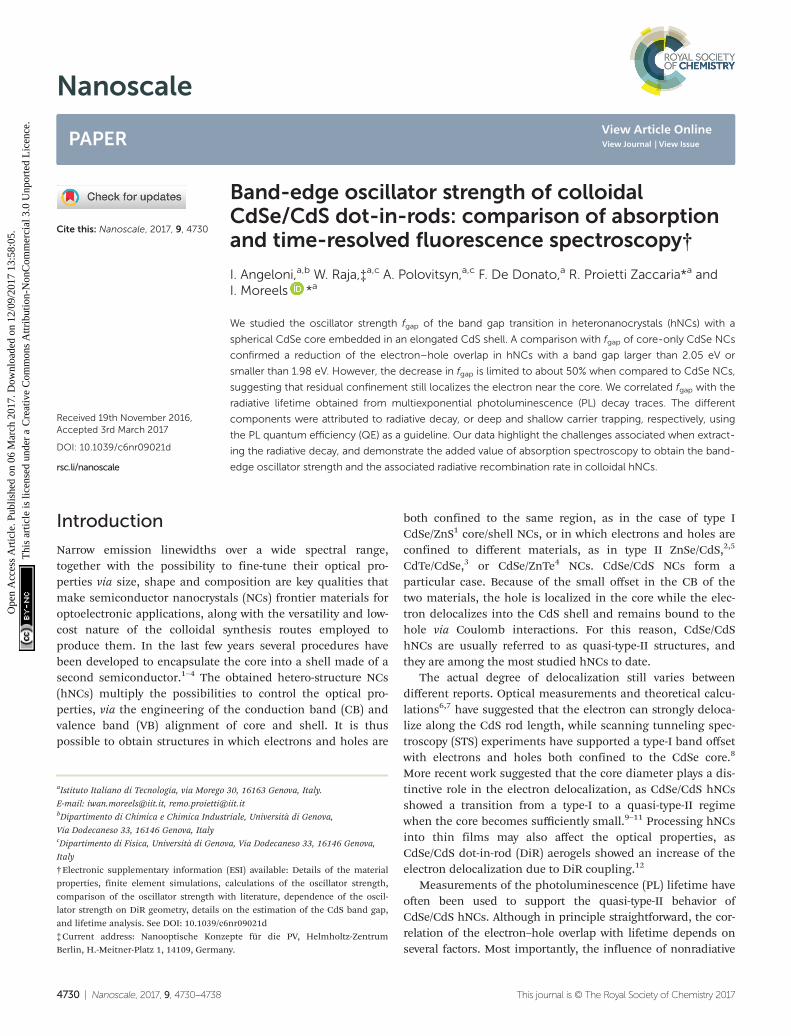
general function to calculate μi of CdSe/CdS hNCs at 4.2 eVthat incorporates the effects of AR and the volume ratio. Herewe make use of this function to calculate the intrinsic absorp-tion spectra for all NCs as μ(v) = (μ4.2/A4.2)·A(v). Representativeμi-spectra of CdSe/CdS DiRs are shown in Fig. 1a.
As μi depends on the core-to-shell volume ratio, band-edgeabsorption properties are more conveniently analyzed usingthe absorption cross section σi = VNC·μi, since it expresses theproperties of a single NC (VNC equals the NC volume). Theσi-spectra are shown in Fig. 1b. The energy-integrated absorp-tion cross section σgap of the band edge transition is obtainedby doubling the integral of the low energy half of the firstabsorption peak in the σi-spectra, as depicted in the inset ofFig. 1b, according to procedures applied previously to PbSe,27
PbS27 and PbSe/CdSe NCs.29 If some scattering was present inthe band edge region, we subtracted a linear background fromthe σi-spectrum before the integration.
The oscillator strength fgap is related to σgap via the localfield factor fLF, which expresses the ratio between the electricfield inside the particle and the external applied electricfield:27
fgap ¼ 2ε0nsmece2πℏ
� 1
fLFj j2 �σgap ð2Þ
ε0 is the vacuum permittivity, ns is the refractive index of themedium, me is the free electron mass, c is the speed of light ina vacuum, e is the elementary charge, and ħ is the reduced
Fig. 1 μi (a) and σi (b) spectra of representative DiRs (NR7, NR10, NR20and NR23 of Table S1,† plotted in blue, green, yellow and red lines,respectively). The inset in panel b shows a zoom of the core region. Wehighlighted the area under the low-energy half of the first absorptionpeak.
Paper Nanoscale
4732 | Nanoscale, 2017, 9, 4730–4738 This journal is © The Royal Society of Chemistry 2017
Ope
n A
cces
s A
rtic
le. P
ublis
hed
on 0
6 M
arch
201
7. D
ownl
oade
d on
12/
09/2
017
13:5
8:05
. T
his
artic
le is
lice
nsed
und
er a
Cre
ativ
e C
omm
ons
Attr
ibut
ion-
Non
Com
mer
cial
3.0
Unp
orte
d L
icen
ce.
View Article Online

Planck’s constant, expressed in eV s as σgap is expressed incm2 eV.
First, we calculated σgap and fgap for CdSe cores. We approxi-mated them as spheres, which allows for an analytical calcu-lation of fLF
27,30 (see ESI, section 2.1†). With fgap ranging from2.4 to 8.1 for 2.3 nm to 6.1 nm NCs, the values follow the sametrend as reported by Čapek et al.23 for zinc blende CdSe NCs(see ESI, section 3† for detailed calculations). The somewhatlower fgap obtained here stems mainly from the reduced CdSeoptical constants used.
While the dielectric screening and thus fLF of a concentricspheroid can be expressed in a closed form,31,32 a numericalfinite-element simulation is needed when non-analyticalshapes are involved.18,33–35 Since the band-edge absorption inour hNCs mainly takes place near the CdSe core, we calculatedfLF from the electric field Eloc inside the core. The NCs weremodeled as cylinders capped by two hemispheres. Because ofthe symmetry of the structure, the polarization which buildsup in response to an applied external field is parallel to it, andso is the resulting field inside the NC.18 Hence, it is sufficientto compute Eloc in the two cases where the external field is par-allel and perpendicular to the major axis of the rod, andobtain the average field intensity as |Eloc|
2 = (|E|||2 + 2|E⊥|
2)/3.With an applied external field Eext = 1 V m−1 in the finite-element simulation, the averaged |Eloc|
2 coincides with | fLF|2.
Different approaches have been reported in literature toestimate the position of the CdSe core in CdSe/CdS DiRs syn-thesized by seeded growth. Quantitative analysis on high-resolution TEM (HR-TEM) images performed by Carboneet al.7 situated the core at about 1/3–1/4 of the total rod length.This estimate was later confirmed by selective growth of goldonto the CdSe region of CdSe/CdS DiRs.36 A more symmetricposition of the core along the rod (about 45% of the totallength) has been estimated recently by Diroll et al.37 on thebasis of annular dark field scanning TEM measurements,revealing that the actual core position may depend somewhaton the synthesis conditions. The core position also varies withthe overall rod length, being closer to the NC center for shortrods, and gradually shifting toward one tip for longersamples.38,39 In order to evaluate the influence of the coreposition on the electric field profile, we performed a finiteelement simulation in which the seed was moved from a posi-tion at 10% to 50% of the total rod length. The results show a15% increase of | fLF|
2 as the CdSe core is located closer to therod center (see ESI, section 2.2†). Note that the changes in|fLF|
2 are more pronounced near the tips, where we find thestrongest non-uniformity of the electric field. | fLF|
2 onlychanges by 3% when the position is varied from 30% to thecenter of the DiR.
Considering the above results, we located the core at 30%of the total length for further calculations. The simulated elec-tric field magnitude along the rod is shown in Fig. 2a for a NCwith AR = 7.5. As expected, the increasing AR leads to a larger|fLF|
2 (Fig. 2b). Simulated data have been fitted using exponen-tial functions y = y0 + A exp(−Bx) (| fLF,|||
2: y0 = 0.971, A =−0.882, B = 0.346; | fLF,⊥|
2: y0 = 0.242, A = 0.227, B = 0.711) to
obtain | fLF|2 for each DiR sample and, through eqn (2), fgap.
The details of the calculation of fgap are reported in the ESI,section 4.†
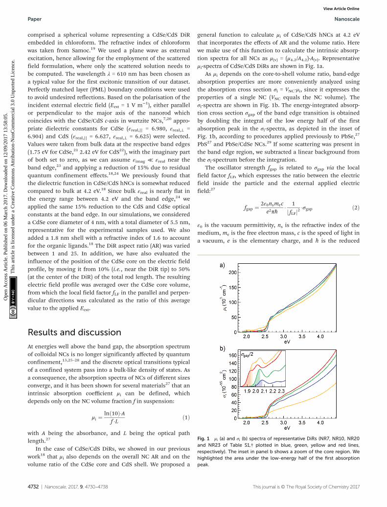
fgap eliminates the role of fLF and the associated shape-dependent σgap, and hence is more suitable to compare spheri-cal core and rod-like core/shell NCs with respect to the elec-tron–hole overlap. We plotted fgap versus the band gap E0 forDiRs (full circles) and CdSe NCs (open circles, see ESI, TablesS1 and S2† for E0 values) shown in Fig. 3, which allows com-parison of core and core/shell NCs that exhibit similarquantum confinement.40 Indeed, as was demonstrated forCdSe and PbX (X = S, Se) quantum dots (QDs),27 fgap increasesfor larger sizes, which prohibits comparison on the basis of asimilar core diameter. Additionally, fgap is frequency-depen-dent, further motivating the use of E0 as a reference.41 In DiRswith a core diameter below ca. 3.5 nm (E0 > 2.05 eV, see colorbar in Fig. 3) a reduction of fgap of about 50% can be appreci-ated. In an intermediate diameter regime (3.5 nm < d < 4.5 nmor 1.98 eV < E0 < 2.05 eV, see color bar in Fig. 3), fgap for DiRs
Fig. 2 (a) Magnitude |Eloc| of the electric field which builds up insidethe DiR in response to an external applied electric field Eext of 1 V m−1 at610 nm, when Eext is parallel (left) or perpendicular (right) to the NCmajor axis (AR = 7.5). Consistent with literature, the CdSe core waslocated at 30% of the total NC length. (b) Values of | fLF|
2 simulated forDiRs with ARs from 1 to 25 (markers) and fit to the data (dashed lines).Parallel and perpendicular components of | fLF|
2 are plotted with bluecircles and diamonds, respectively. The green triangles and line report| fLF|avg
2, the weighted average of the data and fit.
Nanoscale Paper
This journal is © The Royal Society of Chemistry 2017 Nanoscale, 2017, 9, 4730–4738 | 4733
Ope
n A
cces
s A
rtic
le. P
ublis
hed
on 0
6 M
arch
201
7. D
ownl
oade
d on
12/
09/2
017
13:5
8:05
. T
his
artic
le is
lice
nsed
und
er a
Cre
ativ
e C
omm
ons
Attr
ibut
ion-
Non
Com
mer
cial
3.0
Unp
orte
d L
icen
ce.
View Article Online
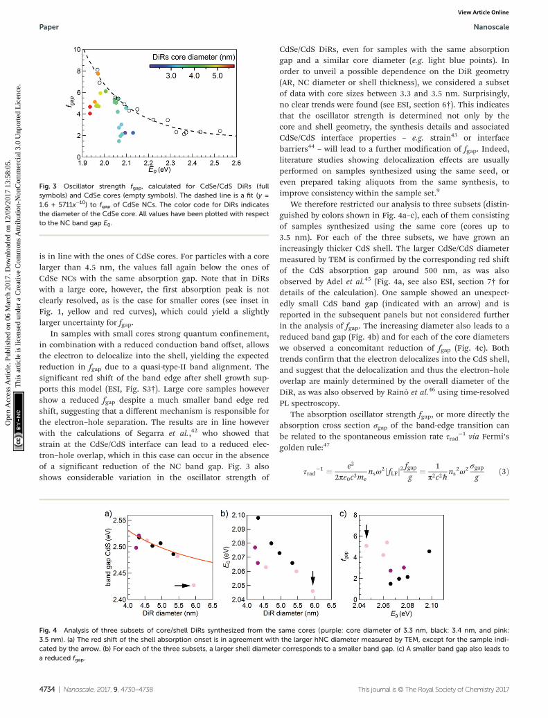
is in line with the ones of CdSe cores. For particles with a corelarger than 4.5 nm, the values fall again below the ones ofCdSe NCs with the same absorption gap. Note that in DiRswith a large core, however, the first absorption peak is notclearly resolved, as is the case for smaller cores (see inset inFig. 1, yellow and red curves), which could yield a slightlylarger uncertainty for fgap.
In samples with small cores strong quantum confinement,in combination with a reduced conduction band offset, allowsthe electron to delocalize into the shell, yielding the expectedreduction in fgap due to a quasi-type-II band alignment. Thesignificant red shift of the band edge after shell growth sup-ports this model (ESI, Fig. S3†). Large core samples howevershow a reduced fgap despite a much smaller band edge redshift, suggesting that a different mechanism is responsible forthe electron–hole separation. The results are in line howeverwith the calculations of Segarra et al.,42 who showed thatstrain at the CdSe/CdS interface can lead to a reduced elec-tron–hole overlap, which in this case can occur in the absenceof a significant reduction of the NC band gap. Fig. 3 alsoshows considerable variation in the oscillator strength of
CdSe/CdS DiRs, even for samples with the same absorptiongap and a similar core diameter (e.g. light blue points). Inorder to unveil a possible dependence on the DiR geometry(AR, NC diameter or shell thickness), we considered a subsetof data with core sizes between 3.3 and 3.5 nm. Surprisingly,no clear trends were found (see ESI, section 6†). This indicatesthat the oscillator strength is determined not only by thecore and shell geometry, the synthesis details and associatedCdSe/CdS interface properties – e.g. strain43 or interfacebarriers44 – will lead to a further modification of fgap. Indeed,literature studies showing delocalization effects are usuallyperformed on samples synthesized using the same seed, oreven prepared taking aliquots from the same synthesis, toimprove consistency within the sample set.9
We therefore restricted our analysis to three subsets (distin-guished by colors shown in Fig. 4a–c), each of them consistingof samples synthesized using the same core (cores up to3.5 nm). For each of the three subsets, we have grown anincreasingly thicker CdS shell. The larger CdSe/CdS diametermeasured by TEM is confirmed by the corresponding red shiftof the CdS absorption gap around 500 nm, as was alsoobserved by Adel et al.45 (Fig. 4a, see also ESI, section 7† fordetails of the calculation). One sample showed an unexpect-edly small CdS band gap (indicated with an arrow) and isreported in the subsequent panels but not considered furtherin the analysis of fgap. The increasing diameter also leads to areduced band gap (Fig. 4b) and for each of the core diameterswe observed a concomitant reduction of fgap (Fig. 4c). Bothtrends confirm that the electron delocalizes into the CdS shell,and suggest that the delocalization and thus the electron–holeoverlap are mainly determined by the overall diameter of theDiR, as was also observed by Rainò et al.46 using time-resolvedPL spectroscopy.
The absorption oscillator strength fgap, or more directly theabsorption cross section σgap of the band-edge transition canbe related to the spontaneous emission rate τrad
−1 via Fermi’sgolden rule:47
τrad�1 ¼ e2
2πε0c3mensω2 fLFj j2 fgap
g¼ 1
π2c2ℏns2ω2 σgap
gð3Þ
Fig. 3 Oscillator strength fgap, calculated for CdSe/CdS DiRs (fullsymbols) and CdSe cores (empty symbols). The dashed line is a fit (y =1.6 + 5711x−10) to fgap of CdSe NCs. The color code for DiRs indicatesthe diameter of the CdSe core. All values have been plotted with respectto the NC band gap E0.
Fig. 4 Analysis of three subsets of core/shell DiRs synthesized from the same cores (purple: core diameter of 3.3 nm, black: 3.4 nm, and pink:3.5 nm). (a) The red shift of the shell absorption onset is in agreement with the larger hNC diameter measured by TEM, except for the sample indi-cated by the arrow. (b) For each of the three subsets, a larger shell diameter corresponds to a smaller band gap. (c) A smaller band gap also leads toa reduced fgap.
Paper Nanoscale
4734 | Nanoscale, 2017, 9, 4730–4738 This journal is © The Royal Society of Chemistry 2017
Ope
n A
cces
s A
rtic
le. P
ublis
hed
on 0
6 M
arch
201
7. D
ownl
oade
d on
12/
09/2
017
13:5
8:05
. T
his
artic
le is
lice
nsed
und
er a
Cre
ativ
e C
omm
ons
Attr
ibut
ion-
Non
Com
mer
cial
3.0
Unp
orte
d L
icen
ce.
View Article Online

ω = E0/ħ is the frequency of the transition and g is the bandgap degeneracy, commonly considered to be 8 for Cd chalco-genides. The PL decay rate has been a subject of investigationsince early studies on CdSe/CdS DiRs.7,48,49 However, theinterpretation of the experimental PL decay traces of CdSecores or CdSe/CdS DiRs is not straightforward, as the decaytypically has to be fitted with a sum of several exponentialfunctions.7,40 Understanding which of these components con-tribute to the radiative emission is crucial if we want tocompare the experimental results with the decay rate calcu-lated theoretically via the absorption cross section. In thisrespect, the QE has often been used to calculate the radiativedecay τrad from the measured PL decay τPL as τrad = τPL/QE.6,7,48,49 However, Gao and Peng14 showed that, in CdSe QDsthat have multi-exponential decays, the component corres-ponding to the intrinsic radiative decay channel is about26–27 ns and independent of the QE, while the changes in QEare associated with the appearance of additional fast decaychannels. These components correspond to the formation ofmid-gap states which function as hole traps. In addition, arelatively slow decay component can often be discerned and isassociated with shallow electron traps on the NC surface thatare in thermal equilibrium with the band-edge state.14,15 Incontrast to the nonradiative hole trapping, this delayed emis-sion does not necessarily lead to a substantial reduction of thePL QE.15 A scheme of possible carrier relaxation pathways isdepicted in Fig. 5a.
To verify the influence of the QE on the radiative lifetime,we measured the PL decay of 3 representative samples, excitingthem at both 405 nm – which is the typical excitation wave-length used throughout our measurements – and 510 nm, awavelength below the CdS band gap that directly excites CdSecore states. The resulting curves were fitted with a multi-expo-nential function using three decay constants. In Fig. 5b, whilethe QE changes by almost a factor of 2 between 405 nm and530 nm, the decay traces exciting at 405 and 510 nm divergeonly in the long tail. Assigning the first two components to theradiative recombination (cf. analysis below and in the ESI,section 9†), the lifetimes calculated are almost identical, yield-ing 22.8 ns and 20.4 ns when exciting at 405 nm and 510 nm,respectively (Table 1). Other samples show a similar behavior(see ESI, section 8†). It confirms that the QE of CdSe/CdSDiRs, excited at 405 nm, is mainly determined by nonradiativerecombination of charge carriers in the CdS shell,38 and therecombination dynamics of core excitons is largely indepen-dent of the excitation wavelength (and thus of the PL QE). ThePL QE is not unity even when exciting the DiRs at 530 nm, yetthis may be due to the existence of a dark fraction of NCs.50
Hence, in the subsequent analysis we do not rely on the QE asa conversion factor between the measured and the radiativelifetime and use it only to classify the DiRs and understandthe PL decay dynamics.
We measured the PL QE (λex = 530 nm, i.e., excitation belowthe CdS absorption edge), and collected the decay traces ofseveral DiR samples (λex = 405 nm), which were then againfitted with a multi-exponential function with three com-
ponents. By analyzing the lifetime and their relative weights,we attributed these individual components to either radiativedecay, fast hole trapping, or shallow electron trapping thatinduces a long-lifetime tail. A detailed discussion of the ana-lysis is reported in the ESI, section 9.† Briefly, when the PL QEfalls below 60%, some DiRs show a low-weight PL componentwith a lifetime below 10 ns, which we considered to be due tononradiative trapping. On the other hand, independent of thePL QE almost all samples revealed a long-lifetime componentwith a lifetime above 100 ns, which was assigned to delayedemission.15 The remaining component(s) were used to calcu-late τrad. A plot of the lifetime components against PL QE, withopen symbols marking trapping and closed symbols markingradiative processes, is shown in Fig. 6a. Note that, with respectto the dataset used for the oscillator strength calculation (seeabove), one sample has been discarded because of a PL QEbelow 3% (NR22 in Table S1†).
Table 1 Lifetime components (and corresponding weights) obtainedfrom the fit of the decay traces shown in Fig. 5, and the radiative lifetimeτrad, calculated considering only the first two decay components
λex τ1 (w1) τ2 (w2) τrad τ3 (w3)
405 nm 15.8 ns (46%) 29.6 ns (48%) 22.8 ns 203.4 ns (6%)510 nm 10.8 ns (15%) 22.2 ns (79%) 20.4 ns 79.9 ns (6%)
Fig. 5 (a) Scheme of the carrier relaxation pathways, highlighting therelaxation processes that lead to radiative emission (full arrows) and thenon-radiative recombination (dashed arrows). k denotes the rates atwhich each process occurs. (b) PL decay traces of a representative DiR(NR12 in Table S1†) upon excitation at 405 nm (green trace) and 510 nm(orange trace). QE values at 405 nm and 530 nm are also reported.
Nanoscale Paper
This journal is © The Royal Society of Chemistry 2017 Nanoscale, 2017, 9, 4730–4738 | 4735
Ope
n A
cces
s A
rtic
le. P
ublis
hed
on 0
6 M
arch
201
7. D
ownl
oade
d on
12/
09/2
017
13:5
8:05
. T
his
artic
le is
lice
nsed
und
er a
Cre
ativ
e C
omm
ons
Attr
ibut
ion-
Non
Com
mer
cial
3.0
Unp
orte
d L
icen
ce.
View Article Online

τrad is compared with literature data for CdSe cores14,51–53
shown in Fig. 6b (see ESI, section 10† for details). As for theanalysis of fgap, the CdSe cores compare well with DiRsbetween 1.98 and 2.05 eV, in agreement with a negligible elec-tron delocalization. Note that, depending on the AR, the life-times of DiRs can even be faster (up to 38%) than CdSe QDswith a similar band gap, due to a larger average local fieldfactor for anisotropic particles (Fig. 2, green triangles). On theother hand, for small and large cores, with a band gap above2.05 eV or below 1.98 eV, respectively, τrad exceeds the CdSecore-only QDs. However, with overall values below 50 ns, τrad isalmost one order of magnitude smaller than in sphericalCdSe/CdS giant shell NCs, where τrad can extend to 500 ns.20,54
This highlights the importance of the NC size and shape indetermining the electron–hole overlap in CdSe/CdS quasi-type-II hNCs via quantum confinement, more specifically strong 2Delectron confinement along the radial direction in DiRs vs.residual weak 3D confinement in giant-shell dot-in-dots(DiDs), and the shape-dependent electron–hole Coulomb inter-actions and dielectric screening.20,54
Using eqn (3), we obtained the emission oscillator strengthfgap,PL from τrad, which we compared with fgap calculated fromthe absorption cross section (denoted as fgap,abs in Fig. 7a).
While reasonable agreement between the two is obtained forsamples with a small core using g = 8, a clear deviation isobserved for other samples. By assuming that the total oscil-lator strength of the transitions involved in the band-edgeabsorption and emission should be equal, we can derive aneffective degeneracy g of the transition. As shown in Fig. 7b,g can reach values ranging from 4 up to 21 for DiRs (fullsymbols). The deviation from g = 8 is not specific to CdSe/CdSDiRs, as we also calculated a continuous increase with corediameter for CdSe QDs (solid line). Likely, it is due tothe energy separation between the bands, which in both casesis strongly reduced for larger QDs, resulting in a larger mani-fold of states located under the first absorption peak. This wasalso reported by Gong et al.,40 who demonstrated that athermal population of the 1p3/2 hole level has to be taken intoaccount at room temperature, as the energy distance betweenthe 1se–1s3/2 and 1se–1p3/2 states is in the range of 21 to 57 meVfor particles from 5.5 to 2.5 nm. These values are comparablewith the typical FWHM of the first absorption peak of oursamples (see ESI, Table S1†). A similar conclusion was drawnfor CdTe NCs by Kamal et al.,55 where good agreement
Fig. 6 (a) Lifetime components obtained from the multi-exponential fitof the DiRs, plotted with respect to the PL QE. Closed (open) symbolsrepresent components which have been attributed to radiative (trapping)processes. (b) Comparison of τrad calculated for our DiRs with literaturedata on CdSe NCs.
Fig. 7 (a) Comparison of the oscillator strength values fgap,abs obtainedfrom the absorption cross section with fgap,PL calculated from theradiative lifetimes, assuming a band gap degeneracy of 8. (b) Effectivedegeneracy of the band edge transition calculated from the ratiobetween fgap,abs and fgap,PL for DiRs (full symbols, with the colour rep-resenting fgap,abs). Similar results for CdSe NCs (solid black line, derivedfrom the fitted curves to the CdSe data shown in Fig. 3 and 6b).
Paper Nanoscale
4736 | Nanoscale, 2017, 9, 4730–4738 This journal is © The Royal Society of Chemistry 2017
Ope
n A
cces
s A
rtic
le. P
ublis
hed
on 0
6 M
arch
201
7. D
ownl
oade
d on
12/
09/2
017
13:5
8:05
. T
his
artic
le is
lice
nsed
und
er a
Cre
ativ
e C
omm
ons
Attr
ibut
ion-
Non
Com
mer
cial
3.0
Unp
orte
d L
icen
ce.
View Article Online

between experimental and measured data was found onlywhen assuming g = 16.
Conclusions
We combined absorption and PL spectroscopy to study theband-edge optical properties of CdSe/CdS hNCs. To this end,fgap is a most convenient quantity, as it directly correlates withthe electron–hole overlap and hence gives insight into thedegree of electron delocalization into the CdS shell. Weobtained fgap for CdSe cores through a calibration of the NCabsorbance spectra at high energy and analytical calculation ofthe electric field inside the core, while finite element simu-lations were needed for the DiRs, as the rod-like shape of theshell leads to a non-uniform internal electric field. The com-parison of fgap for CdSe NCs and CdSe/CdS DiR hNCs shows areduced electron–hole overlap both in the limit of small(below 3.5 nm) and large (above 4.5 nm) CdSe core diameters.While in the first case this is the result of electron delocaliza-tion into the CdS shell, with the extent of delocalizationmainly determined by the rod diameter, in the latter it is poss-ibly enabled by strain at the core/shell interface.42
Independent results are obtained when fgap,PL is calculatedfrom the radiative lifetimes via Fermi’s golden rule. Here, con-tributions to the decay traces were separated into radiative pro-cesses and nonradiative trapping, and we observed that the PLQE cannot be used to directly extract τrad from the measuredPL decay time. fgap,PL obtained from the DiR radiative decaycorroborated the results from absorption spectroscopy.Different from spherical giant-shell CdSe/CdS DiDs, whereradiative lifetimes can reach 500 ns,20,54 radiative lifetimesremain overall shorter than 50 ns in DiRs, making them idealcandidates for applications where a high absorption crosssection and PL QE need to be combined with fast recombina-tion rates.56,57
Acknowledgements
The present publication is realized with the support of theMinistero degli Affari Esteri e della CooperazioneInternazionale (IONX-NC4SOL).
References
1 M. A. Hines and P. Guyot-Sionnest, J. Phys. Chem., 1996,100, 468–471.
2 A. Nemchinov, M. Kirsanova, N. N. Hewa-Kasakarage andM. Zamkov, J. Phys. Chem. C, 2008, 112, 9301–9307.
3 D. Oron, M. Kazes and U. Banin, Phys. Rev. B: Condens.Matter, 2007, 75, 035330.
4 S. Kim, B. Fisher, H.-J. Eisler and M. Bawendi, J. Am. Chem.Soc., 2003, 125, 11466–11467.
5 D. Dorfs, A. Salant, I. Popov and U. Banin, Small, 2008, 4,1319–1323.
6 J. Müller, J. M. Lupton, P. G. Lagoudakis, F. Schindler,R. Koeppe, A. L. Rogach, J. Feldmann, D. V. Talapin andH. Weller, Nano Lett., 2005, 5, 2044–2049.
7 L. Carbone, C. Nobile, M. De Giorgi, F. D. Sala, G. Morello,P. Pompa, M. Hytch, E. Snoeck, A. Fiore, I. R. Franchini,M. Nadasan, A. F. Silvestre, L. Chiodo, S. Kudera,R. Cingolani, R. Krahne and L. Manna, Nano Lett., 2007, 7,2942–2950.
8 D. Steiner, D. Dorfs, U. Banin, F. Della Sala, L. Manna andO. Millo, Nano Lett., 2008, 8, 2954–2958.
9 A. Sitt, F. D. Sala, G. Menagen and U. Banin, Nano Lett.,2009, 9, 3470–3476.
10 H. Eshet, M. Grünwald and E. Rabani, Nano Lett., 2013, 13,5880–5885.
11 X. Wen, A. Sitt, P. Yu, Y.-R. Toh and J. Tang, Phys. Chem.Chem. Phys., 2012, 14, 3505–3512.
12 S. Sánchez-Paradinas, D. Dorfs, S. Friebe, A. Freytag,A. Wolf and N. C. Bigall, Adv. Mater., 2015, 27, 6152–6156.
13 J. Jasieniak, L. Smith, J. van Embden, P. Mulvaney andM. Califano, J. Phys. Chem. C, 2009, 113, 19468–19474.
14 Y. Gao and X. Peng, J. Am. Chem. Soc., 2015, 137, 4230–4235.
15 F. T. Rabouw, M. Kamp, R. J. A. van Dijk-Moes,D. R. Gamelin, A. F. Koenderink, A. Meijerink andD. Vanmaekelbergh, Nano Lett., 2015, 15, 7718–7725.
16 M. J. Barthel, I. Angeloni, A. Petrelli, T. Avellini,A. Scarpellini, G. Bertoni, A. Armirotti, I. Moreels andT. Pellegrino, ACS Nano, 2015, 9, 11886–11897.
17 M. Grabolle, M. Spieles, V. Lesnyak, N. Gaponik,A. Eychmüller and U. Resch-Genger, Anal. Chem., 2009, 81,6285–6294.
18 I. Angeloni, W. Raja, R. Brescia, A. Polovitsyn, F. DeDonato, M. Canepa, G. Bertoni, R. Proietti Zaccaria andI. Moreels, ACS Photonics, 2016, 3, 58–67.
19 A. Samoc, J. Appl. Phys., 2003, 94, 6167–6174.20 S. Christodoulou, G. Vaccaro, V. Pinchetti, F. De Donato,
J. Q. Grim, A. Casu, A. Genovese, G. Vicidomini, A. Diaspro,S. Brovelli, L. Manna and I. Moreels, J. Mater. Chem. C,2014, 2, 3439.
21 S. Ninomiya and S. Adachi, J. Appl. Phys., 1995, 78, 4681–4689.
22 S. Ninomiya and S. Adachi, J. Appl. Phys., 1995, 78, 1183–1190.
23 R. K. Čapek, I. Moreels, K. Lambert, D. De Muynck,Q. Zhao, A. Van Tomme, F. Vanhaecke and Z. Hens, J. Phys.Chem. C, 2010, 114, 6371–6376.
24 M. Alves-Santos, R. D. Felice and G. Goldoni, J. Phys. Chem.C, 2010, 114, 3776–3780.
25 C. A. Leatherdale, W.-K. Woo, F. V. Mikulec andM. G. Bawendi, J. Phys. Chem. B, 2002, 106, 7619–7622.
26 P. Yu, M. C. Beard, R. J. Ellingson, S. Ferrere, C. Curtis,J. Drexler, F. Luiszer and A. J. Nozik, J. Phys. Chem. B, 2005,109, 7084–7087.
27 Z. Hens and I. Moreels, J. Mater. Chem., 2012, 22, 10406.28 M.-A. Langevin, D. Lachance-Quirion, A. M. Ritcey and
C. N. Allen, J. Phys. Chem. C, 2013, 117, 5424–5428.
Nanoscale Paper
This journal is © The Royal Society of Chemistry 2017 Nanoscale, 2017, 9, 4730–4738 | 4737
Ope
n A
cces
s A
rtic
le. P
ublis
hed
on 0
6 M
arch
201
7. D
ownl
oade
d on
12/
09/2
017
13:5
8:05
. T
his
artic
le is
lice
nsed
und
er a
Cre
ativ
e C
omm
ons
Attr
ibut
ion-
Non
Com
mer
cial
3.0
Unp
orte
d L
icen
ce.
View Article Online

29 B. De Geyter, Y. Justo, I. Moreels, K. Lambert, P. F. Smet,D. Van Thourhout, A. J. Houtepen, D. Grodzinska, C. deMello Donega, A. Meijerink, D. Vanmaekelbergh andZ. Hens, ACS Nano, 2011, 5, 58–66.
30 C. F. Bohren and D. R. Huffman, Absorption and Scatteringof Light by Small Particles, Wiley-VCH Verlag GmbH, 1998.
31 A. H. Sihvola and J. A. Kong, IEEE Trans. Geosci. RemoteSens., 1988, 26, 420–429.
32 S. Giordano, J. Electrost., 2003, 58, 59–76.33 J. Venermo and A. Sihvola, J. Electrost., 2005, 63, 101–117.34 A. Sihvola, P. Yla-Oijala, S. Jarvenpaa and J. Avelin, IEEE
Trans. Antennas Propag., 2004, 52, 2226–2233.35 A. Mejdoubi and C. Brosseau, Phys. Rev. E: Stat. Phys.,
Plasmas, Fluids, Relat. Interdiscip. Top., 2006, 74, 031405.36 G. Menagen, D. Mocatta, A. Salant, I. Popov, D. Dorfs and
U. Banin, Chem. Mater., 2008, 20, 6900–6902.37 B. T. Diroll, N. Gogotsi and C. B. Murray, Chem. Mater.,
2016, 3345–3351.38 K. Wu, L. J. Hill, J. Chen, J. R. McBride, N. G. Pavlopolous,
N. E. Richey, J. Pyun and T. Lian, ACS Nano, 2015, 9, 4591–4599.
39 E. Yoskovitz, G. Menagen, A. Sitt, E. Lachman andU. Banin, Nano Lett., 2010, 10, 3068–3072.
40 K. Gong, Y. Zeng and D. F. Kelley, J. Phys. Chem. C, 2013,117, 20268–20279.
41 J. Johansen, S. Stobbe, I. S. Nikolaev, T. Lund-Hansen,P. T. Kristensen, J. M. Hvam, W. L. Vos and P. Lodahl, Phys.Rev. B: Condens. Matter, 2008, 77, 073303.
42 C. Segarra, J. I. Climente, A. Polovitsyn, F. Rajadell,I. Moreels and J. Planelles, J. Phys. Chem. Lett., 2016, 7,2182–2188.
43 F. Rajadell, M. Royo and J. Planelles, J. Appl. Phys., 2012,111, 014303.
44 N. J. Borys, M. J. Walter, J. Huang, D. V. Talapin andJ. M. Lupton, Science, 2010, 330, 1371–1374.
45 P. Adel, J. Bloh, D. Hinrichs, T. Kodanek and D. Dorfs,Z. Phys. Chem., 2016, 93–106.
46 G. Rainò, T. Stöferle, I. Moreels, R. Gomes, Z. Hens andR. F. Mahrt, ACS Nano, 2012, 6, 1979–1987.
47 E. Merzbacher, Quantum Mechanics, Wiley InternationalEdition, New York, 2nd edn, 1970.
48 D. V. Talapin, J. H. Nelson, E. V. Shevchenko, S. Aloni,B. Sadtler and A. P. Alivisatos, Nano Lett., 2007, 7, 2951–2959.
49 C. She, A. Demortière, E. V. Shevchenko and M. Pelton,J. Phys. Chem. Lett., 2011, 2, 1469–1475.
50 N. Durisic, A. G. Godin, D. Walters, P. Grütter, P. W. Wisemanand C. D. Heyes, ACS Nano, 2011, 5, 9062–9073.
51 A. F. van Driel, G. Allan, C. Delerue, P. Lodahl, W. L. Vosand D. Vanmaekelbergh, Phys. Rev. Lett., 2005, 95, 236804.
52 C. de Mello Donegá and R. Koole, J. Phys. Chem. C, 2009,113, 6511–6520.
53 H.-M. Gong, Z.-K. Zhou, H. Song, Z.-H. Hao, J.-B. Han,Y.-Y. Zhai, S. Xiao and Q.-Q. Wang, J. Fluoresc., 2007, 17,715–720.
54 S. Brovelli, R. D. Schaller, S. A. Crooker, F. García-Santamaría, Y. Chen, R. Viswanatha, J. A. Hollingsworth,H. Htoon and V. I. Klimov, Nat. Commun., 2011, 2, 280.
55 J. S. Kamal, A. Omari, K. Van Hoecke, Q. Zhao,A. Vantomme, F. Vanhaecke, R. K. Capek and Z. Hens,J. Phys. Chem. C, 2012, 116, 5049–5054.
56 A. Castelli, F. Meinardi, M. Pasini, F. Galeotti, V. Pinchetti,M. Lorenzon, L. Manna, I. Moreels, U. Giovanella andS. Brovelli, Nano Lett., 2015, 15, 5455–5464.
57 E. Jang, S. Jun, H. Jang, J. Lim, B. Kim and Y. Kim, Adv.Mater., 2010, 22, 3076–3080.
Paper Nanoscale
4738 | Nanoscale, 2017, 9, 4730–4738 This journal is © The Royal Society of Chemistry 2017
Ope
n A
cces
s A
rtic
le. P
ublis
hed
on 0
6 M
arch
201
7. D
ownl
oade
d on
12/
09/2
017
13:5
8:05
. T
his
artic
le is
lice
nsed
und
er a
Cre
ativ
e C
omm
ons
Attr
ibut
ion-
Non
Com
mer
cial
3.0
Unp
orte
d L
icen
ce.
View Article Online