paper electronics using environmentally friendly and phase
TRANSCRIPT

Paper Electronics using Environmentally Friendly and Phase Separated
Semiconductor/Insulator Blends 14.8 2013
1F. Pettersson, 2J. Koskela, 1,3T. Remonen, 3Y. Zhang, 3S. Inkinen, 4R. Bollström, 5A. Määttänen, 5P. Ihalainen, 2A. Kilpelä, 3C-E. Wilén, 4M. Toivakka, 5J. Peltonen
and 1R. Österbacka 1Department of Natural Sciences/Physics at Åbo Akademi University, Porthaninkatu 3-5, FI-20500 Turku, Finland.
2Electronics Laboratory at University of Oulu, PL 45000 FI-90014, Finland. 3Department of Chemical ENgineering/Polymer Tehnology at Åbo Akademi University, Piispankatu 3, FI-20500 Turku, Finland. 4Department of CHemical Engineering/Paper Coating and Converting at Åbo Akademi University, Porthaninkatu3-5, FI-20500
Turku,Finland. 5Department of Natural Sciences/Physical Chemistry at Åbo Akademi University, Porthaninkatu3-5, FI-20500 Turku,Finland.

Motivation
• Paper electronics can potentially be cheap (R2R compatible) and recyclable and can be used for instance for sensing and detecting
• Making R2R compatible low-voltage transistors on paper that are fast and on paper that is not coated with plastic – HIFET on recyclable paper R. Bollström et al. Org. Electron. 2009, 10, 1020
– ECT on paper R. Mannerbro et al. Synth. Met. 2008, 158, 556
2 0.5 0.0 -0.5 -1.0 -1.5 -2.01E-3
0.01
0.1
1
10
ID
IS
IG
VD= -1.5 V
Cu
rre
nts
(A
)
Gate voltage (V)

Ion modulation
3
OFET Traditional dielectric Electrolyte Polyelectrolyte
Ion modulated OFET
~30 nF/cm2 100 μF/cm2 20 μF/cm2
M.J. Panzer, C.R. Newman, C.D. Frisbie, Appl. Phys. Lett. 86 (2005) 103503 E. Said, X. Crispin, L. Herlogsson, S. Elhag, N.D. Robinson, M. Berggren, Appl. Phys. Lett. 89 (2006) 143507 A.R. Brown, C.P. Jarrett, D.M. de Leeuw, M. Matters, Synthetic Met. 88 (1997) 37–55

Lateral structure
Advantages:
• Fewer fabrication steps
• Less sensitivity to roughness
• No alignment issues
• Avoid problem with printing gate on top of insulator
• Insulator can be liquid
• Favorable for sensor application
Disadvantages:
• Speed
4
Drain
Source
Semiconductor
Ion Gel
Gate
The use of ion-gels as gate dielectric allows for the use of lateral transistor structure with higher capacitance value
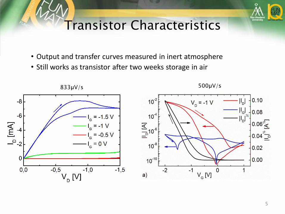
Transistor Characteristics
5
• Output and transfer curves measured in inert atmosphere
• Still works as transistor after two weeks storage in air
833µV/s 500µV/s

Ring oscillator
6
R = 205 k VDD = -0.8 V Oscillation frequency:105 µHz Propagation delay time: 870 s
• We have built an electric circuit using our paper transistors
– A ring oscillator with 5 inverters

Improving the speed
• The volume of the semiconductor dictates speed: – Electrochemical doping during operation => Bulk transport
• Solutions:
– Reduce device dimensions:
• Print the whole device
– Make the semiconductor thinner
• Fabricating thin semiconductor on porous paper problematic
7

Thinner semiconductor
• Use semiconductor/insulator blend to get spontaneous vertical phase separation (surface energy, solubility)
• SC separated from paper => No doping of SC by OH-groups in paper
8

Device performance
9
10 nm 90 nm

Improving the speed
• 200 times faster scan speed and no hysteresis!
10
100 mV/s 0.5 mV/s

Improving the speed
• The rise time of transistors with different concentration blends were measured
• Notice logarithmic time scale!
11
0 10 20 30 40 50 60 70 801
10
100
1000
10000
5
10
15
20
[s
]
CP3HT
[%]
|IG| [n
A]
|IG|

Ring oscillator
• Propagation delay time decreased from 870 s to 35 ms. More than 4 orders of magnitude improvement!
12
R1,2 = 1 M R3 = 2.2 M VDD = -2.5 V, -3 V Oscillation frequency:5 Hz Propagation delay time: 35 ms

Environmentally Friendly IL
• The ion gel used is not environmentally friendly.
• We can make ion modulated transistors that are suitable also for food packages.
• Replace EMIM-TFSI with environmentally friendly ion gels
13

• Create ionic liquids that have bulky anions
• Use base and different complexators to create deep eutectic mixtures
Environmentally Friendly IL
14

Definitions
15 VG
ION
-1.0 -0.8 -0.6 -0.4 -0.2 0.0
1E-10
1E-9
1E-8
1E-7
0.0000
0.0002
0.0004
|ID
,G| [A
]
VG [V]
|ID|
|IG|
|ID|½
|ID|½
[A
½]
V0 Vt
IOFF

• PET substrate, P3HT as SC, different IL drops as dielectric and probing station as gate
Different ILs
16

Conclusions
17
• We have created a low-voltage organic transistor on paper with high output current that works in air
• We have built fast ring-oscillators on paper using environmentally friendly phase separated SC/INS blends
• We have replaced the harmful EMIM:TFSI IL with environmentally friendly one

Thank you