packet telemetry encoder (ptme) vhdl...
TRANSCRIPT

PTME-001-01Version 0.7 rev 2September 2005
Först Långgatan 19 tel +46 31 7758650413 27Göteborg fax +46 31 421407Sweden www.gaisler.com
Packet Telemetry Encoder (PTME) VHDL ModelData Sheet
Prepared by Sandi Habinc

PTME-001-01 2
Table of contents
1 INTRODUCTION............................................................................................ 51.1 Scope ................................................................................................................ 51.2 Introduction ...................................................................................................... 51.3 Applicable standards and limitations ............................................................... 51.4 Commissioned and non-commissioned functions............................................ 51.5 Configuration at compile time and during operation ....................................... 51.6 Not implemented .............................................................................................. 51.7 Applicable documents ...................................................................................... 61.8 Applicable VHDL source code ........................................................................ 61.9 Reference documents ....................................................................................... 61.10 Acronyms and abbreviations ............................................................................ 71.11 Reed-Solomon code patent............................................................................... 81.12 Turbo code patent............................................................................................. 81.13 Change history.................................................................................................. 8
2 CONVENTIONS.............................................................................................. 92.1 Advanced Microcontroller Bus Architecture ................................................... 92.2 Consultative Committee for Space Data Systems............................................ 92.3 Galois Field ...................................................................................................... 92.4 Telemetry Transfer Frame format .................................................................... 102.5 Reed-Solomon encoder data format ................................................................. 112.6 Turbo encoder data format ............................................................................... 122.7 Attached Synchronisation Marker.................................................................... 122.8 Command Link Control Word ......................................................................... 132.9 Source Packet ................................................................................................... 132.10 Asynchronous bit serial data format................................................................. 142.11 Waveform formats............................................................................................ 14
3 OVERVIEW..................................................................................................... 15
4 MODULE SPECIFICATIONS ........................................................................ 164.1 Packet Telemetry Encoder (PTME) ................................................................. 164.2 Telemetry Encoder (TME) ............................................................................... 174.2.1 Implementation options selected at compile time ............................................ 174.2.2 Transfer Frame generation ............................................................................... 184.2.3 Bandwidth allocation and selection.................................................................. 244.2.4 Time strobe....................................................................................................... 244.2.5 Virtual Channels............................................................................................... 254.3 Reed-Solomon Encoder (RSE)......................................................................... 324.4 Turbo Encoder (TE) ......................................................................................... 344.5 Pseudo-Randomiser (PSR) ............................................................................... 364.6 Non-Return-to-Zero Mark encoder (NRZ)....................................................... 364.7 Convolutional Encoder (CE) ............................................................................ 364.8 Split-Phase Level modulator (SP) .................................................................... 374.9 Clock Divider (CD) .......................................................................................... 37

PTME-001-01 3
5 MODULE DESCRIPTIONS............................................................................ 385.1 Telemetry Encoder (TME) ............................................................................... 385.2 Virtual Channel Encoder (VCE) ...................................................................... 395.2.1 Virtual Channel Assembler (VCA) .................................................................. 395.2.2 Virtual Channel Multiplexer (VCM)................................................................ 415.2.3 Virtual Channel Buffer (VCB) ......................................................................... 445.3 Reed-Solomon Encoder (RSE)......................................................................... 525.3.1 Adder ................................................................................................................ 545.3.2 Check symbol memory..................................................................................... 545.3.3 Parallel multiplier ............................................................................................. 545.3.4 Serial shift and parallel hold registers .............................................................. 545.3.5 Control.............................................................................................................. 545.4 Turbo Encoder (TE) ......................................................................................... 555.4.1 Interleaver......................................................................................................... 575.4.2 Constituent encoders ........................................................................................ 575.4.3 Table................................................................................................................. 575.4.4 Control.............................................................................................................. 575.5 Pseudo-Randomiser (PSR) ............................................................................... 585.6 Non-Return-to-Zero Mark encoder (NRZ)....................................................... 585.7 Convolutional Encoder (CE) ............................................................................ 595.8 Split-Phase Level modulator (SP) .................................................................... 605.9 Clock Divider (CD) .......................................................................................... 615.10 Packet Telemetry Encoder (PTME) ................................................................. 645.10.1 Connectivity ..................................................................................................... 645.10.2 Limitations........................................................................................................ 65
6 MODULE INTERFACES................................................................................ 666.1 Multiple input interfaces .................................................................................. 666.2 Virtual Channel Interface (VCI) definition ...................................................... 666.3 PTME Internal Bus (PIB or PI-bus) definition ................................................ 676.4 Virtual Channel Request (VCR) definition ...................................................... 67
7 PTME DESIGN OPTIONS.............................................................................. 68
8 PTME INTERFACES ...................................................................................... 708.1 System interface ............................................................................................... 748.2 Bit rate interface ............................................................................................... 748.3 Memory allocation interface ............................................................................ 748.4 General configuration interface........................................................................ 748.5 Virtual Channel Assembler configuration interfaces ....................................... 768.6 Virtual Channel Interface (VCI)....................................................................... 778.7 PacketWire (PW) input interface ..................................................................... 788.8 PacketAsynchronous (PA) input interface ....................................................... 798.9 PacketParallel (PP) input interface................................................................... 798.10 PacketAPB (PAPB) input interface.................................................................. 808.11 Memory test interface....................................................................................... 828.12 Memory interface ............................................................................................. 828.13 EDAC interface ................................................................................................ 828.14 AMBA AHB master interface.......................................................................... 83

PTME-001-01 4
8.15 Telemetry test interface .................................................................................... 858.16 Channel Access Data Unit output interface ..................................................... 858.17 Bandwidth Allocation Table interface ............................................................. 868.18 Operation Control Field / CLCW / TTC-B-01 interface.................................. 87
9 PTME VHDL SOURCE CODE DESCRIPTION............................................ 889.1 Packages and libraries, interface port and generic types.................................. 889.2 Compilation order............................................................................................. 889.3 Simulation ........................................................................................................ 889.4 Model hierarchy ............................................................................................... 89
APPENDIX A: THEORETICAL BACKGROUND ON REED-SOLOMON CODING 90A.1 Reference documents .............................................................................. 90A.2 Reed-Solomon encoding......................................................................... 90A.3 Galois fields ............................................................................................ 93A.4 Derivation of ESA standard from CCSDS recommendation.................. 98A.5 Parallel multiplication in dual basis........................................................ 103

PTME-001-01 5
1 INTRODUCTION
1.1 Scope
This document describes the Packet Telemetry Encoder (PTME) VHDL model. The objectiveis to describe the VHDL model at a level of detail allowing its integration into an overall system.It is not the objective to describe the VHDL model to a level of detail allowing modifications orusage of individual modules in the model hierarchy.
1.2 Introduction
The purpose of the Packet Telemetry Encoder (PTME) synthesizable VHDL model is to providethe user with a single module implementing the Consultative Committee for Space DataSystems (CCSDS) recommendations for telemetry and channel coding.
1.3 Applicable standards and limitations
The PTME model is based on the European Space Agency (ESA) Procedures, Standards andSpecifications (PSS) and the CCSDS recommendations. The model has been specified tosupport both sets of standards as far as possible. Any discrepancies due to conflicts between thetwo sets have been explained in the text. At the time of writing there were no relevantdocuments available from the European Cooperation for Space Standardization (ECSS).
1.4 Commissioned and non-commissioned functions
The PTME model has been partitioned in commissioned and in non-commissionedfunctionalities. The non-commissioned functionalities have been classified as such because notproperly verified or validated, because the interfaces of the functions are not user oriented, orbecause a function might be removed in a future revision of the model. Non-commissionedfunctions are not described in detail in this document.
The main non-commissioned functionalities are listed hereafter and are repeated in the text:• Telemetry test interface on the boundary of the PTME• Virtual Channel Interface (VCI) on the boundary of the PTME• Dynamic memory allocation interface on the boundary of the PTME• Physical addressing on the PTME Internal Bus (PIB)• Memory test interface on the boundary of the PTME, based on the PTME Internal Bus (PIB)
1.5 Configuration at compile time and during operation
The PTME VHDL model can be configured at compile or synthesis time to include variousfunctions in a design. The resulting instantiation of the design can then be configured duringoperation to enable the use of implemented functions. It is important to recognise the difference.
1.6 Not implemented
The PTME VHDL model does not implement the following:• Telemetry Encoder does not support Reed-Solomon encoding interleave depths 3 and 8.• The length of received Source/Telemetry Packets must be greater than the on-chip input
buffers of the Telemetry Encoder (see gLength generic).

PTME-001-01 6
1.7 Applicable documents
AD1 Packet Telemetry Standard, ESA PSS-4-106, Issue 1, January 1988AD2 Packet Telemetry, CCSDS 102.0-B-5, Issue 5, November 2000
AD3 Telemetry Channel Coding Standard, ESA PSS-04-103, Issue 1, September 1989AD4 Telemetry Channel Coding. CCSDS 101.0-B-5, Issue 6, October 2002
AD5 Radio Frequency and Modulation Standard, ESA PSS-04-105, Issue 1, Dec. 1989
AD6 Packet Telecommand Standard, ESA PSS-04-107, Issue 2, April 1992AD7 Telecommand: Part 2 - Data Routing Service, CCSDS 202.0-B-3, June 2001AD8 Telecommand Decoder Specification, ESA PSS-04-151, Issue 1, September 1993
AD9 AMBATM Specification, Rev 2.0, ARM IHI 0011A, 13 May 1999, Issue A, firstrelease, ARM Limited
AD10 RS-232 EIA/TIA Standard
1.8 Applicable VHDL source code
AD11 Packet Telemetry Encoder (PTME) synthesizable VHDL model, version 0.8c,February 2004, ptme_lib.vhd
AD12 AMBA synthesizable VHDL package, version 0.5, February 2002, amba.vhd
1.9 Reference documents
RD1 Space Data Communication, ESA PSS-04-0, March 1991RD2 Telemetry Summary Concept and Rationale, CCSDS 100.0.G-1, December 1997RD3 Packet Telemetry Service Specification, CCSDS 103.0-B-2, Issue 2, June 2001
RD4 ESA VHDL Modelling Guidelines, ASIC/001, Issue 1, September 1994RD5 IEEE Standard VHDL Language Reference Manual, IEEE Std 1076-1993RD6 IEEE Standard Multivalue Logic System for VHDL Model Interoperability
(Std_Logic_1164), IEEE Std 1164-1993RD7 IEEE Standards Interpretations: IEEE Standard VHDL Language Reference Manual,
IEEE Std 1076/INT-1991
RD8 Bit Serial Encoder, E. Berlekamp, European Patent Specification, publication number 0 066 618, 24 September 1986
RD9 US4410989: Bit serial encoder, Elwyn R. Berlekamp, Cyclotomics, Inc., 11 December 1980
RD10 US5446747: Error-correction coding method with at least two systematic convolutional codings in parallel, corresponding iterative decoding method, decoding module and decoder, Claude Berrou, France Télécom, 16 April 1992

PTME-001-01 7
1.10 Acronyms and abbreviations
AHB Advanced High-performance Bus (AMBA interface)AMBA Advanced Microcontroller Bus Architecture TM
APB Advanced Peripheral Bus (AMBA interface)AOS Advanced Orbiting SystemsASIC Application Specific Integrated CircuitASM Attached Synchronisation MarkerBAT Bandwidth Allocation TableCCSDS Consultative Committee for Space Data SystemsCD Clock DividerCE Convolutional EncoderCLCW Command Link Control WordCRC Cyclic Redundancy CodeDMA Direct Memory AccessECSS European Cooperation for Space StandardizationEDAC Error Detection and CorrectESA European Space AgencyFECW Frame Error Control WordFHP First Header PointerFPGA Field Programmable Gate ArrayGF Galois FieldLFSR Linear Feedback Shift RegisterNRZ Non Return to ZeroOPCF Operational Control FieldPA PacketAsynchronousPAPB PacketAPBPIB PTME Internal Bus (internal PTME interface)PP PacketParallelPSR Pseudo RandomiserPSS Procedures, Standards and SpecificationsPW PacketWireRSE Reed-Solomon EncoderSEU Single Event UpsetSP Split-PhaseTE Turbo Encoder TM TelemetryTME Telemetry EncoderVC Virtual ChannelVCA Virtual Channel AssemblerVCB Virtual Channel BufferVCE Virtual Channel EncoderVCI Virtual Channel Interface (internal PTME interface)VCM Virtual Channel MultiplexerVCR Virtual Channel Request (internal PTME interface)

PTME-001-01 8
1.11 Reed-Solomon code patent
The Reed-Solomon encoder implementations previously used by the European Space Agency(ESA) have been based on the bit serial encoder patented by Berlekamp under US Patent4,410,989 (RD9) and its counterparts in other countries (RD8). That architecture exploitsmaximum resource sharing by implementing all Galois field operations bit serially. The core ofthe encoder is the bit serial multiplier which can perform the Galois field multiplication using aserial shift register and some combinatorial logic. The patent relies on the usage of a Galois fieldrepresentation that has a dual basis, which enables bit serial multiplication. The ESA andCCSDS telemetry channel coding standard Galois Field representation has a dual basis, since ithas been selected for envisaged implementations using the Berlekamp encoder.
The benefits of the bit serial multiplier are insignificant when implementing a monolithicencoder. A bit serial encoder approach using a parallel multiplier only adds a marginal areaoverhead. The benefit of such an approach is that the encoder can be used without restrictionssince the Berlekamp patent is not infringed. The Reed-Solomon Encoder (RSE) described inthis document is therefore based on a bit serial implementation with a parallel multiplier.
1.12 Turbo code patent
Implementers should be aware that a wide class of turbo codes is covered by a patent by FranceTélécom and Télédiffusion de France under US Patent 5,446,747 (RD10) and its counterpartsin other countries. Potential user agencies should direct their requests for licenses to:
Mr. Christian HamonCCETT GIE/CVP4 rue du Clos Courtel, BP59, 35512 CESSON SEVIGNE Cedex, FranceTel: +33 2 99 12 48 05, Fax: +33 2 99 12 40 98
1.13 Change history
In version 0.4 the ClockDivider only operates on BitClk, which can be divided to generate anoutput bit rate frequency. A separate input has been added, IdleSegmentLen, to set the SegmentLength Identifier bits in Idle Transfer Frames when output on a separate Virtual Channel inorder to avoid conflicts between CCSDS and ESA PSS recommendations. The Reed-SolomonE=8 (255, 239) code is fully integrated. Flexible Virtual Channel Identifier allocation has beenadded. Support for 16 and/or 32 bit OPCF data transfer has been added.
In version 0.5 the packet abort function is fully integrated, but the packet length check functionhas been removed completely. The CLCW interface functionality has been extended. Thelatency requirements for the Turbo encoder has been reduced. The relation between telemetrybit rate and system clock has been improved.
In version 0.6 the telemetry channel encoders are controlled by means of generics instead ofconstants defined in a package. For the overall PTME however, the same constants are still usedto define what values are to be assigned to said generics. Improved usage of the Conv_UnSignedfunctions has been implemented in the definition package to avoid synthesis problems.
In version 0.7 a buffer empty indicator was introduced for each VCA.

PTME-001-01 9
2 CONVENTIONS
2.1 Advanced Microcontroller Bus Architecture
Convention according to the Advanced Microcontroller Bus Architecture (AMBA)Specification, AD9, applying to the AHB and APB interfaces:• Signal names are in upper case, except for the following: • A lower case 'n' in the name indicates that the signal is active low. • Constant names are in upper case.• The least significant bit of an array is located to the right, carrying index number zero.
2.2 Consultative Committee for Space Data Systems
Convention according to the Consultative Committee for Space Data Systems (CCSDS)recommendations, applying to all relevant structures:• The most significant bit of an array is located to the left, carrying index number zero, and is
transmitted first.• An octet comprises eight bits.
General convention, applying to signals and interfaces:• Signal names are in mixed case.• An upper case '_N' suffix in the name indicates that the signal is active low.
2.3 Galois Field
Convention according to the Consultative Committee for Space Data Systems (CCSDS)recommendations, applying to all Galois Field GF(28) symbols:• A Galois Field GF(28) symbol comprises eight bits.• The least significant bit of a symbol is located to the left, carrying index number zero, and is
transmitted first.
AMBA n-bit fieldmost significant least significant
n-1 n-2 down to 1 0
Table 1: AMBA n-bit field definition
CCSDS n-bit fieldmost significant least significant
0 1 to n-2 n-1
Table 2: CCSDS n-bit field definition
Galois Field GF(28) symbolleast significant most significant
0 1 to 6 7
Table 3: Galois Field GF(28) symbol definition

PTME-001-01 10
2.4 Telemetry Transfer Frame format
The telemetry Transfer Frame specified in AD1 and AD2 is composed of a Primary Header, aSecondary Header, a Data Field and a Trailer with the following structures.
Transfer FrameTransfer Frame Header Transfer Frame Data Field Transfer Frame Trailer
Primary Secondary (optional) ket | Packet | Pa OPCF / FECW (optional)6 octets 0 / 4 octets variable 0 / 2 /4 / 6 octets
223 / 446 / 892 / 1115 / 239 / 478 / 956 / 1195 octets
Table 4: Transfer Frame format
Transfer Frame Primary HeaderFrame Identification Master
Channel FrameCount
Virtual Channel FrameCount
FrameDataFieldStatus
Version S/CId
VCId
OPCFFlag
2 bits0:1
10 bits2:11
3 bits12:14
1 bit15
8 bits 8 bits 16 bits
2 octets 1 octet 1 octet 2 octets
Table 5: Transfer Frame Primary Header format
Frame Data Field Status
Secondary Header Flag Sync Flag Packet Order Flag Segment Length Id First Header Pointer
1 bit0
1 bit1
1 bit2
2 bits3:4
11 bits5:15
2 octets
Table 6: Part of Transfer Frame Primary Header format
Transfer Frame Secondary Header (optional)Secondary Header Identification Secondary Header Data
Secondary Header Version Secondary Header Length Virtual Channel Frame Count
2 bits0:1
6 bits2:7
24 additional bits0:23
1 octet 3 octets
Table 7: Transfer Frame Secondary Header format
Transfer Frame Trailer (optional)Operational Control Field (optional) Frame Error Control Word (optional)
0 / 4 octets 0 / 2 octets
Table 8: Transfer Frame Trailer format

PTME-001-01 11
2.5 Reed-Solomon encoder data format
The applicable standards AD3 and AD4 specify a Reed-Solomon E=16 (255, 223) coderesulting in the frame lengths and codeblock sizes listed in table 9.
The applicable standards AD4 also specifies a Reed-Solomon E=8 (255, 239) code resulting inthe frame lengths and codeblock sizes listed in table 10.
Interleave depth Attached Synchronisation Marker Transfer Frame Reed-Solomon Check Symbols
1 4 octets 223 octets 32 octets2 446 octets 64 octets3 669 octets 96 octets4 892 octets 128 octets5 1115 octets 160 octets8 1784 octets 256 octets
Table 9: Reed-Solomon E=16 codeblocks with Attached Synchronisation Marker
Interleave depth Attached Synchronisation Marker Transfer Frame Reed-Solomon Check Symbols
1 4 octets 239 octets 16 octets2 478 octets 32 octets3 717 octets 48 octets4 956 octets 64 octets5 1195 octets 80 octets8 1912 octets 128 octets
Table 10: Reed-Solomon E=8 codeblocks with Attached Synchronisation Marker

PTME-001-01 12
2.6 Turbo encoder data format
The applicable standard AD4 specifies four Turbo code information block lengths k. It alsospecifies four code rates r. The resulting Turbo encoded block size is dependent on both theinformation block length and the code rate, n=32/r + (k+4)/r, as shown in table 13.
2.7 Attached Synchronisation Marker
The Attached Synchronisation Marker pattern depends on the encoding scheme in use, asspecified in AD4 and shown in table 14.
Information block length [bits] Information block length [octets] Reed-Solomon interleave depth
1784 223 13568 446 27136 892 48920 1115 5
Table 11: Turbo encoder information block length as per AD4
Information block
length k [bits]
Codeblock length n [bits]
rate 1/2 rate 1/3 rate 1/4 rate 1/6
1784 3576 5364 7152 107283568 7144 10716 14288 214327136 14280 21420 28560 428408920 17848 26772 35696 53544
Table 12: Turbo codeblock lengths as per AD4
Attached Synchronisation MarkerTurbo Codeblock
Encoded Transfer Frame Trellis Termination
32/r bits k/r bits 4/r bits
Table 13: Structure of a Turbo encoded block as per AD4
Mode Hexadecimal stream (left to right)
Nominal 1ACFFC1Dh
Alternative 352EF853h
Rate 1/2 turbo encoded 034776C7272895B0h
Rate 1/3 turbo encoded 25D5C0CE8990F6C9461BF79Ch
Rate 1/4 turbo encoded 034776C7272895B0 FCB88938D8D76A4Fh
Rate 1/6 turbo encoded 25D5C0CE8990F6C9461BF79C DA2A3F31766F0936B9E40863h
Table 14: Attached Synchronization Marker hexadecimal pattern

PTME-001-01 13
2.8 Command Link Control Word
The Command Link Control Word (CLCW) can be transmitted as part of the Operation ControlField (OPCF) in a Transfer Frame Trailer. The CLCW is specified in AD6 and AD7 and is listedin table 15, table 16 and table 17.
2.9 Source Packet
The Source Packet defined in the ESA PSS AD1 standard and the CCSDS AD2recommendation is used in this document and is listed in table 18, although the SegmentationFlags are interpreted differently in the two referenced documents. The Telemetry Packet definedin ESA PSS AD1 standard has also this same format, although the Packet Length and Data Fieldare interpreted differently. The differences have no effect on the commissioned part of theTelemetry Encoder (TME).
Command Link Control WordStatic part Dynamic part
Generated by the Telemetry Encoder (TME), or from external data interface
From external data interface
0:15 16:3116 bits 16 bits
Table 15: Command Link Control Word overview
Static part of the Command Link Control WordControl Word Type Version Number Status Field COP in Effect Virtual Channel Identifier Reserved Field
0 1:2 3:5 6:7 8:13 14:151 bit 2 bits 3 bits 2 bits 6 bits 2 bits
Table 16: Command Link Control Word static part
Dynamic part of the Command Link Control WordNo RF Available No Bit Lock Lock Out Wait Retransmit FARM B Counter Report Type Report Value
16 17 18 19 20 21:22 23 24:311 bit 1 bit 1 bit 1 bit 1 bit 2 bits 1 bit 8 bits
Table 17: Command Link Control Word dynamic part
Source Packet / Telemetry PacketPacket Header Packet Data Field
Packet Identification Packet Sequence Control PacketLength
Data FieldHeader
(optional)
SourceData
Packet ErrorControl
(optional)VersionNumber
Type Data FieldHeader Flag
ApplicationProcess Id
SegmentationFlags
SourceSequence
Count0:2 3 4 5:15 16:17 18:31 32:47
3 bits 1 bit 1 bit 11 bits 2 bits 14 bits 16 bits variable variable variable
Table 18: Source Packet and Telemetry Packet format

PTME-001-01 14
2.10 Asynchronous bit serial data format
The asynchronous bit serial interface complies to the data format defined in AD10. It alsocomplies to the data format and waveform shown in table 19 and figure 1. The interface isindependent of the transmitted data contents. Positive logic is considered for the data bits. Thenumber of stop bits can optionally be either one or two. The parity bit can be optionallyincluded, although the value of the bit is not used in the design described this document.
2.11 Waveform formats
The Packet Telemetry Encoder (PTME) accepts and generates the waveform formats shown inthe following figures.
Figure 1: Asynchronous bit serial waveform
Figure 2: Synchronous bit serial waveform
Figure 3: Synchronous bit serial waveform, Telemetry Interface (AD8)
Asynchronous bit serial format
start D0 D1 D2 D3 D4 D5 D6 D7 parity stop stopfirst lsb msb last
General data formati = {0, n}
8*i+7 8*i+6 8*i+5 8*i+4 8*i+3 8*i+2 8*i+1 8*ilast first
Table 19: Asynchronous bit serial data format
D0 D1 D2 D3 D4 D5 D6 D7start parity stoplsb msb stop
P
Delimiter
Clock
Data 0 1 2 3 4 5 6 7 0 1 2 3 4 5 6 70 1 2 376
Sampling
Clock
Data 0 1 2 3 4 5 6 7 n-3 n-2 n-1n-7 n-6 n-5 n-4n-8
PTME-001-01 15
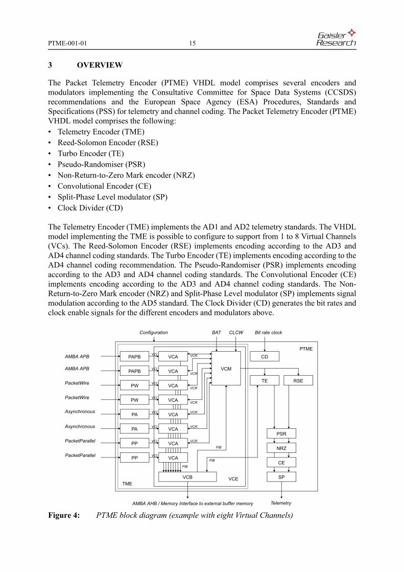
3 OVERVIEW
The Packet Telemetry Encoder (PTME) VHDL model comprises several encoders andmodulators implementing the Consultative Committee for Space Data Systems (CCSDS)recommendations and the European Space Agency (ESA) Procedures, Standards andSpecifications (PSS) for telemetry and channel coding. The Packet Telemetry Encoder (PTME)VHDL model comprises the following:• Telemetry Encoder (TME)• Reed-Solomon Encoder (RSE)• Turbo Encoder (TE)• Pseudo-Randomiser (PSR)• Non-Return-to-Zero Mark encoder (NRZ)• Convolutional Encoder (CE)• Split-Phase Level modulator (SP)• Clock Divider (CD)
The Telemetry Encoder (TME) implements the AD1 and AD2 telemetry standards. The VHDLmodel implementing the TME is possible to configure to support from 1 to 8 Virtual Channels(VCs). The Reed-Solomon Encoder (RSE) implements encoding according to the AD3 andAD4 channel coding standards. The Turbo Encoder (TE) implements encoding according to theAD4 channel coding recommendation. The Pseudo-Randomiser (PSR) implements encodingaccording to the AD3 and AD4 channel coding standards. The Convolutional Encoder (CE)implements encoding according to the AD3 and AD4 channel coding standards. The Non-Return-to-Zero Mark encoder (NRZ) and Split-Phase Level modulator (SP) implements signalmodulation according to the AD5 standard. The Clock Divider (CD) generates the bit rates andclock enable signals for the different encoders and modulators above.
Figure 4: PTME block diagram (example with eight Virtual Channels)
VCE
PW
RSE
PSR
NRZ
CD
VCM
VCB
PA
PTME
VCA
VCA
VCA
VCA VCR
VCR
VCR
VCI
PIB
VCI
VCI
VCI
Asynchronous
PacketWire
Telemetry
Bit rate clock
VCAVCI VCR
VCR
PAPB
PWPacketWire
AMBA APB
PAPBAMBA APB
VCI
VCIPPPacketParallel
PAAsynchronous VCA
VCAPIB
VCR
VCR
TE
CEPIB
TME
AMBA AHB / Memory Interface to external buffer memory
VCAVCIPPPacketParallel
CLCWBATConfiguration
SP
PTME-001-01 16
4 MODULE SPECIFICATIONS
The Packet Telemetry Encoder (PTME) VHDL model comprises a set of modules implementingthe embedded encoders and modulators. The overall specification of each module will bediscussed in this section. It should be noted that it is not always possible to utilise all thespecified capabilities of each module in the PTME due to architectural constraints.
4.1 Packet Telemetry Encoder (PTME)
The Packet Telemetry Encoder (PTME) module always instantiates the following modules:• Telemetry Encoder (TME)• Clock Divider (CD)
The PTME module can be configured at compile time to instantiate separately each of thefollowing modules:• Reed-Solomon Encoder (RSE)• Turbo Encoder (TE)• Pseudo-Randomiser (PSR)• Non-Return-to-Zero Mark encoder (NRZ)• Convolutional Encoder (CE)• Split-Phase Level modulator (SP)
The PTME module provides the interconnection between the different encoders and supports allpermissible coding chains. It facilitates an external telemetry test interface, although notcommissioned, to allow telemetry insertion to the Reed-Solomon Encoder (RSE) and TurboEncoder (TE), bypassing the Telemetry Encoder (TME). The symbol output of the last encoderin the coding chain is routed to the output interface of the PTME for which a re-synchronisationof the signal is performed to avoid glitch generation.
The PTME module combines the internal unidirectional data buses of the memory interface toa single bidirectional data bus interface. This is also done for the Bandwidth Allocation Table(BAT) interface data bus.
Is should be noted that the Telemetry Encoder (TME) module is not a separate entity in thePTME VHDL model. It is merely a constellation of modules related to the telemetry encodingprocess. The description given in this document is principally oriented around the functionalstructure rather than the implementation oriented structure of the PTME VHDL model. Detailswill be provided in section 5.1. For time being it is sufficient to state that the PTME moduleinstantiates the components constituting the TME.

PTME-001-01 17
4.2 Telemetry Encoder (TME)
The Telemetry Encoder (TME) generates telemetry data according to ESA PSS standard AD1and CCSDS recommendation AD2. The TME incorporates the user interfaces to the telemetryencoder, the control of the temporary buffering of user data, the generation of the telemetryTransfer Frame, the downlink bandwidth arbitration between Virtual Channels, and the controlof subsequent encoders and modulators.
4.2.1 Implementation options selected at compile time
The TME can be configured at compile time to provide a variety of services, each option beingselected individually. All configuration options are listed in section 7. The most importantoptions are explained in this section, having a substantial impact on the implemented design.
The number of Virtual Channels to be implemented is selectable between one and eight. TheVirtual Channel Identifiers are assigned automatically sequentially beginning at 0, or viaexternal input when flexible allocation is selected. It is possible to generate Idle telemetryTransfer Frames on any of the implemented channels or on a separate Virtual Channel on whichno user data can be transmitted.
The different Virtual Channels share a common external buffer memory in which data receivedon the user interfaces are temporarily stored. The sizing and splitting of the external buffermemory between the Virtual Channels is fixed to some extent at compile time. The followingparameters are set: the overall memory size, the number of areas into which the memory is split,the number of areas that can be grouped and allocated to any Virtual Channel.
Support for alternative Attached Synchronisation Marker (ASM) generation, as per AD1, canbe selected. Support for Secondary Header generation, Version-1 as per AD1, can be selected.Support for Operation Control Field (OPCF) generation can be selected. It is also possible toselect non-standard 32 bit wide OPCF insertion. Selection between a serial synchronousinterface or a parallel implementation for the OPCF data input is supported. Support for FrameError Control Word (FECW) generation can be selected. Support for time strobe generation canbe selected. The Bandwidth Allocation Table (BAT) is used for the arbitration of the downlinkbandwidth and the following interfaces can be selected: no interface, asynchronous memorytype interface, or the BAT can be implemented outside the TME (and PTME). Support forimplementing 223 octet based and/or 239 octet based frame lengths is provided.
Several parameters control the implementation of each individual Virtual Channel and theirinterfaces. The following parameters are configurable at compile time. Support for packethandling can be selected, generating the First Header Pointer dynamically. Support for IdleSource Packet insertion can be selected. Support for external buffer memory availabilityindication can be selected. Support for user abort of packet input can be selected. The inputinterface to the Virtual Channel can be selected from one of the following options: PacketWire(PW), PacketAsynchronous (PA), PacketParallel (PP), PacketAPB (PAPB) with associated datawidth selection, or direct connection via the Virtual Channel Input (VCI) which is an internalinterface format and is not commissioned. The number of memory areas allocated to the VirtualChannels can either be done statically at compile time or dynamically via an external interface,the latter not being commissioned.

PTME-001-01 18
4.2.2 Transfer Frame generation
The Telemetry Encoder (TME) generates the telemetry Transfer Frame according to AD1 andAD2 as described in the subsequent sections. Some of the fields in the Transfer Frame areoptional, of which some are indicated by means of flags in the Primary Header and the inclusionof other fields is handled by management rather than by the communication protocol.
4.2.2.1 Operational configuration
The encoder allows the following fields to be enabled/disabled or varied during operation,provided that the corresponding implementation option has been selected at compile time. Theencoder should be reset after a configuration change.• Nominal or alternative Attached Synchronisation Marker• Time strobe periodicity• Transfer Frame length• Spacecraft Identifier• Virtual Channel Identifier allocation• Transfer Frame Secondary Header (selected individually per Virtual Channel)• Operation Control Field (selected collectively for all Virtual Channels)• Frame Error Control Field• Blank space generation for Reed-Solomon check symbols• Blank space generation for Turbo code trellis termination
4.2.2.2 Attached Synchronisation Marker
The encoder always generates an Attached Synchronisation Marker (ASM) in front of theTransfer Frame. The encoder generates a 32 bit long ASM. The other ASM lengths listed intable 14, are produced by subsequent encoders. The encoder is always capable of generating thenominal ASM as listed in table 14. If selected at compile time, the encoder can also produce thealternative ASM listed in table 14. The alternative ASM can be used when a stream of TransferFrames is embedded as data in another stream using the nominal ASM. The encoder implementsone output stream for which either the nominal or alternative ASM will be produced at a time.
4.2.2.3 Transfer Frame lengths
The TME supports the Transfer Frame lengths listed in table 20.
Transfer Frame length choice Transfer Frame lengths
000b 223 octets001b 446 octets010b 892 octets011b 1115 octets100b 239 octets101b 478 octets110b 956 octets111b 1195 octets
Table 20: Transfer Frame length alternatives

PTME-001-01 19
4.2.2.4 Transfer Frame Primary Header
The Transfer Frame Primary Header format is listed in table 6.
4.2.2.4.1 Frame Identification
The Transfer Frame Version Number is permanently set to 00b (Version-1). The VersionNumber can be only modified by changing a constant in the source code, which is notrecommended.
The Spacecraft Identifier is configurable during operation.
The Virtual Channel Identifier is dynamically generated, depending on what Virtual Channelhas been chosen for transmission in the Transfer Frame being composed. The Virtual Channelselection is described in section 4.2.3. If the TME has been configured at compile time tosupport flexible Virtual Channel Identifier allocation, it is possible to configure the individualVirtual Channel Identifier fields via an external input, provided that the encoder is reset inbetween changes. The Virtual Channel Identifier used for Idle Transfer Frames is set at compiletime when flexible allocation is not selected.
The Operational Control Field Flag is configurable during operation and indicates whether ornot the Operation Control Field (OPCF) is included in the Transfer Frame, provided the optionis selected at compile time. The OPCF is transferred in all Transfer Frames when enabled.
4.2.2.4.2 Master Frame Counter
The Master Frame Counter is an 8 bit wide modulo 256 sequential binary counter, incrementedfor each transmitted Transfer Frame.
4.2.2.4.3 Virtual Channel Frame Counter
There is one Virtual Channel Frame Counter for each Virtual Channel implemented. The VirtualChannel Frame Counter is an 8 bit wide modulo 256 sequential binary counter, incremented foreach Transfer Frame in which the associated Virtual Channel is transmitted. The VirtualChannel Frame Counter width can be extended to 32 bits as described in section 4.2.2.5.
4.2.2.4.4 Frame Data Field Status
The Frame Data Field Status is associated with the Virtual Channel being transmitted in theTransfer Frame.
The Secondary Header Flag indicates whether or not a Transfer Frame Secondary Header istransmitted in the Transfer Frame. It is possible to enable the transmission of the SecondaryHeader on a per Virtual Channel basis, as declared valid in the CCSDS AD2 recommendation.
The Data Field Synchronisation Flag indicates whether packets are synchronously inserted,when 0b, or whether data are asynchronously inserted, when 1b, in the Data Field of the TransferFrame. Refer to the ESA telemetry standard AD1 for a detailed definition

PTME-001-01 20
The Packet Order Flag indicates in which order packets have been inserted in the Data Field.The flag is only used as a data bit by the TME and has no other effect on its operation.
The Segment Length Identifier selects the maximum field length of the standard TelemetryPackets inserted in the Transfer Frame. The identifier is only used as data bits by the TME andhas no other effect on its operation.
The First Header Pointer is required for the packet chaining process during packet de-multiplexing on the ground. The encoder generates Transfer Frames in the active or idle modeas defined in AD1. The data contained in an active Transfer Frame can be either packets or non-packet data. Packets are referred to as synchronous data in AD1, whereas non-packet data arereferred to as asynchronous data. Since packets may be of varying lengths, it is unlikely that aninteger number of packets will be exactly contained within a Transfer Frame Data Field, somepackets will consequently be split between two Transfer Frames. The encoder calculates theposition of the first octet of the first packet to be placed in each Transfer Frame, in accordancewith AD1, and then inserts this value into the First Header Pointer (FHP) field in the TransferFrame. The FHP is initiated to all ones at reset. If a packet is longer than the data field of theTransfer Frame, the FHP is set to all ones. The encoder fully supports the FHP formation anddoes not require any alignment of the data with the Transfer Frame boundary.
Part of the Frame Data Field Status field for the Idle Transfer Frames described insection 4.2.2.6.3 is fixed in the encoder. The Data Field Synchronisation Flag is 0b, since idledata is inserted as per AD2. The Packet Order Flag is 0b. The First Header Pointer is set to thepredefined Idle First Header Pointer code. This code is the same both for packet and non-packetdata: 11111111110b.
4.2.2.5 Transfer Frame Secondary Header
The generation of the Secondary Header specified in the ESA PSS AD1 standard is supportedby the TME. If this option is selected, the support for Secondary Header generation will beimplemented for all Virtual Channels. The TME allows the Secondary Header to be included oromitted individually for each Virtual Channel, as permitted in the CCSDS AD2recommendation. The ESA PSS AD1 standard only allows the inclusion or omission to be donecollectively for all Virtual Channels.
4.2.2.5.1 Secondary Header Identifier
The Secondary Header Version Number is permanently set to 00b (Version-1). The SecondaryHeader Length field is permanently set to 000011b, indicating a length for the entire SecondaryHeader of four octets.

PTME-001-01 21
4.2.2.5.2 Secondary Header Data
The Secondary Header Data field contains an additional 24 bits of the Virtual Channel FrameCounters associated with the transmitted Transfer Frame. These bits are the 24 most significantbits of the resulting extended Virtual Channel Frame Counter of 32 bits. The 8 least significantbits of the counter are transmitted in the Primary Header Virtual Channel Counter field.
4.2.2.6 Transfer Frame Data Field
The data transmitted in the Transfer Frame Data Field is either user data, defined as the activestate, or when no user data is available, a pseudo-random bit sequence as specified insection 4.2.2.6.3, defined as the idle state.
The information stored in the Transfer Frame Data Field in the active state can either be packets,defined as synchronous insertion, or any other data, defined as asynchronous insertion or bitstreaming. The main difference between the two insertion types is the generation of the FirstHeader Pointer, which is always dynamic for the former and normally fixed for the latter.
4.2.2.6.1 Supported formats
For the synchronous insertion, the encoder supports all packet formats defined in the CCSDSAD2 recommendation:• Source Packet (Version Number 000b - Version-1)• CCSDS Network Protocol (NP) Datagram• Internet Protocol Datagram (IPv4)• Encapsulation Packet
For the synchronous insertion, the encoder additionally supports the packet formats defined inthe ESA PSS AD1 standard:• Source Packet (Version Number 100b - Version-2)• Telemetry Packet (Version Number 100b - Version-2)
The encoder actually supports any privately defined or future data format for synchronous datainsertion since being largely independent of the data contents.
The encoder supports any privately defined data format for asynchronous data insertion into theTransfer Frame Data Field. It also provides the possibility for dynamic First Header Pointergeneration for asynchronous insertion, although not endorsed by the ESA PSS and CCSDStelemetry standards and recommendations.
For the Idle Source Packet insertion function described in section 4.2.5.3, both the SourcePacket and the Telemetry Packet formats are supported. The Segment Length Flags are set to
MSB 32 bit Virtual Channel Frame Counter LSB
0 23 24 31
MSB Secondary Header Data LSB MSB Virtual Channel Frame Count LSB
0 23 0 7
Table 21: Virtual Channel Frame Counter definition

PTME-001-01 22
11b, which means that the Source Packet is identical to the Telemetry Packet since nosegmentation is performed (Version-2) or no packet grouping is performed (Version-1). TheVersion Number can be set during operation.
4.2.2.6.2 Data fetch
The Transfer Frame Data Field is fetched from the external buffer memory area allocated to theVirtual Channel selected for transmission in the Transfer Frame. The Transfer Frame generationprocess is not concerned with the content of the data being fetched. The data reception processin the interface of each individual Virtual Channel is however concerned with the datadelimiting, and in some cases the contents, as described in section 4.2.5.
4.2.2.6.3 Idle Transfer Frame generation
When there is insufficient data available from the implemented Virtual Channels to complete aData Field, the encoder generates an Idle Transfer Frame on the fly. The Idle Transfer FrameData Field need not to contain any useful data and is filled with a pseudo-random bit sequence.The pseudo-random generator polynomial is h(x) = x9+x4+1 and is implement as a many-to-one implementation, which is a Fibonacci version of a Linear Feed-back Shift Register (LFSR),with x0 as output. The pseudo-random generator is free-running, but is only shifted once foreach bit generated for the Data Field. The generator is initialized to all ones at reset and eachtime the associated Virtual Channel Frame Counter reaches zero. In this way the contents of theData Field are deterministic and are possible to reproduce on ground provided that the VirtualChannel Frame Counter value is known for the Transfer Frame being analysed.
The encoder can implement a separate Virtual Channel for Idle Transfer Frame generation oruse one of the Virtual Channels implemented for user data transfers. This is selectable atcompile time at which the Virtual Channel Identifier is set for the Idle Transfer Frame creation,when flexible Virtual Channel Identifier allocation is not selected.
4.2.2.7 Transfer Frame Trailer
The Transfer Frame Trailer comprises two optional fields; the Operation Control Field and theFrame Error Control Word.
4.2.2.7.1 Operation Control Field
The encoder supports the generation of the Operation Control Field (OPCF) if this option isselected at compile time. It is possible to enable or disable the OPCF insertion during a mission.The OPCF is transmitted in each Transfer Frame if enabled, as specified in the ESA PSS AD1standard and the CCSDS AD2 recommendation. It is not possible to transmit the OPCF inTransfer Frames associated with only a specific Virtual Channel, which is additionallypermitted in AD2.
It is possible to input 16 and/or 32 bits of the OPCF via an external interface, which is selectableat compile time. If both options are implemented, 32 bit insertion can be explicitly enabled viaan input. When 32 bit insertion is used, the format of the OPCF is under user responsibility. Theformat of the OPCF for 16 bit insertion is described hereafter. It is possible to overwrite bits 16and 17 with discrete input values instead of using the information available in the CLCW. Thisoption is enabled by means of a configuration input.
PTME-001-01 23
The first leading bit of the OPCF is the Type Flag. Only the Type-1-Report (Type Flag being 0b)is supported by the encoder. The Type-1-Report contains the Command Link Control Word(CLCW) specified in AD6 and AD7 and listed in table 16 and table 17. The first static part ofthe CLCW is assembled by the encoder, as listed in table 22, and the second dynamic part of theCLCW is received via an external interface, as listed in table 23. The encoder supportsinterfacing of two CLCW sources, by providing two Virtual Channel Identifier inputs that canbe associated with two different Packet Telecommand Decoders.
The encoder implements two interface types for the retrieval of the dynamic part of the CLCW,which are selectable at compile time. To be compatible with existing Packet TelecommandDecoders, the Telemetry Interface specified in AD8 is implemented. The interface is also knowas the TTC-B-01 Serial 16-Bit Digital Channel from an older ESA document. This interfaceprovides two synchronous bit serial channels. For future use, the encoder features a directparallel input for providing the CLCW data, for which the interfacing to multiple sources shouldbe implemented outside the encoder. Both interfaces support 16 and 32 bit data transfer.
4.2.2.7.2 Frame Error Control Word
The encoder supports the generation of the Frame Error Control Word (FECW) if the option isselected at compile time. It is possible to enable or disable the FECW insertion during a mission.The FECW is inserted in all Transfer Frames when enabled. The FECW contains a CyclicRedundant Code (CRC) calculated over the Transfer Frame. The polynomial is g(x) =x16+x12+x5+1 and is a one-to-many implementation, which is a Galois version of a LinearFeed-back Shift Register (LFSR) with x0 as output. The LFSR is initialised to all ones betweenTransfer Frames. The field is known as the Frame Error Control Field (FECF) in AD2.
4.2.2.8 Coding space
The encoder can insert blank space between the end of the Transfer Frame and the beginning ofthe subsequent ASM to accommodate Reed-Solomon and Turbo coding, if individually selectedat compile time. The encoder supports Transfer Frame lengths directly compatible with theE=16 (255, 223) Reed-Solomon code, as specified AD3 and AD4. The appropriate number ofzero-value octets are inserted for each information block length as listed in table 9. The encoderalso supports insertion of zero-value octets in amounts specified for the E=8 (255, 239) Reed-Solomon code as listed in table 10. The encoder supports insertion of four zero-value bits forthe Turbo coding as specified in AD4.
Dynamic/Static part of the Command Link Control WordControl Word Type Version Number Status Field COP in Effect Virtual Channel Identifier Reserved Field
0 1:2 3:5 6:7 8:13 14:150b 00b 000b 01b mission configurable 00b
Table 22: Command Link Control Word dynamic/static part assignment
Dynamic part of the Command Link Control WordNo RF Available No Bit Lock Lock Out Wait Retransmit FARM B Counter Report Type Report Value
16 17 18 19 20 21:22 23 24:31all bits retrieved from external interface
Table 23: Command Link Control Word dynamic part

PTME-001-01 24
4.2.3 Bandwidth allocation and selection
The encoder provides two built-in algorithms for selecting which Virtual Channel to output inthe next Transfer Frame. It is not possible to perform the Virtual Channel selection externallyto the encoder. The Bandwidth Allocation algorithm guarantees a minimum bandwidth for eachVirtual Channel. In this algorithm the encoder uses adaptive channel ordering in order to utilizethe available bandwidth as efficiently as possible. In the Priority Selection algorithm theencoder selects the highest priority Virtual Channel that has a Data Field ready for transmission.
The Bandwidth Allocation Table (BAT) is used for the arbitration of the downlink bandwidthand is used for both algorithms. The following options can be selected at compile time: internalBAT with no interface, internal BAT with asynchronous memory type interface, or the completeBAT is located outside the encoder. For the latter option, all modifications of the BAT contentsmust be done synchronously with the encoder clock or when a write indicator output is assertedby the encoder. The size of the BAT is selectable at compile time.
When the BAT is located in the encoder, it is initialised at reset. It will be initialised to containan incremental sequence of values in the range of the implemented Virtual Channel Identifiers.All Virtual Channels will therefore have a nearly equal bandwidth allocated when theBandwidth Allocation algorithm is selected. If the Priority Selection algorithm is enabled, thisinitialisation sequence will mean that Virtual Channel with identifier zero will have the highestpriority and the Virtual Channel with the highest identifier value will have the lowest priority.For example, in an implementation with four Virtual Channels and 32 entries, the BAT willcontain the following sequence after reset: 0, 1, 2, 3, 0, 1, 2, 3 and so on.
4.2.4 Time strobe
A time strobe is generated according to AD1, being asserted simultaneously with the first bit ofthe Attached Synchronisation Marker output. The timing of the time strobe is not valid if Turboencoding is applied because data buffering takes place. The accuracy of the time strobe isreduced by the usage of other encoders and modulator. Usually the time strobe is beingproduced one bit clock period earlier for each simple encoder in use. The time strobe is assertedfor 128 bit clock periods. The periodicity of the time strobe is configurable during a mission,being linked to the eight least significant bits of the Virtual Channel Frame Counter of VirtualChannel number 0, as listed in table 24.
Time strobe periodicity setting Virtual Channel 0 Frame Count values (8 bits)
0000b 0, 1, 2, 3, 4... 253, 254, 2550001b 0, 2, 4, 6, 8... 250, 252, 2540010b 0, 4, 8, 12, 16... 244, 248, 2520011b 0, 8, 16, 24, 32... 232, 240, 2480100b 0, 16, 32, 48, 64... 208, 224, 2400101b 0, 32, 64, 96, 128, 160, 192, 2240110b 0, 64, 128, 1920111b 0, 1281---b 0
Table 24: Time strobe periodicity

PTME-001-01 25
4.2.5 Virtual Channels
The Virtual Channels in the Telemetry Encoder (TME) are treated as separate entities, eachbeing individually configured during operation.
4.2.5.1 Operational configuration
The encoder allows the following functions or protocol fields to be varied during operation foreach Virtual Channel, provided that the corresponding design option is selected at compile time.
The following fields in the Frame Data Field Status can be configured:• Secondary Header Flag (used as data bit and Secondary Header insertion qualifier)• Data Field Synchronisation Flag (use as data bit and Idle Source Packet generation qualifier)• Packet Order Flag (used as data bit only)• Segment Length Identifier (used as data bits only) as listed in table 25
The following functions can be configured or enabled for the data reception process:• External buffer memory allocation to the Virtual Channel (non-commissioned)• Threshold for external buffer memory availability indication, as listed in table 26• Dynamic or static First Header Pointer calculation, where dynamic calculation must be used
with synchronous data insertion and can be used with asynchronous data insertion (althoughnot endorsed in telemetry standards), and where static calculation must only be used withasynchronous data insertion (independent of Data Field Synchronisation Flag setting above)
For the Idle Source Packet generation the following can be configured during operation:• Version Number (most significant bit, 000b and 100b supported) (used as data bit only)• Threshold for number of polls before generation commences, as listed in table 27 and
explained in section 4.2.5.3
Segment Length Identifier Maximum Data Field length of Telemetry Packets (AD1)
00b 256 octets (only in AD1)01b 512 octets (only in AD1)10b 1024 octets (only in AD1)11b 65536 octets (no segmentation) (both AD1 and AD2)
Table 25: Segment Length Identifier interpretation
Threshold selection Available unused octets in external buffer memory
00b ≥ 262 (256 + 6)01b ≥ 518 (512 + 6)10b ≥ 1030 (1024 + 6)11b ≥ length of Transfer Frame Data Field
Table 26: Threshold setting for external buffer memory availability indication

PTME-001-01 26
4.2.5.2 Data buffering
The Virtual Channels receive data, via the interfaces described later, which are stored in theexternal buffer memory. Each Virtual Channel keeps track of the number of octets received andthe packet boundaries in order to calculate the First Header Pointer discussed insection 4.2.2.4.4. Data are stored in pre-allocated external buffer memory slots comprisingTransfer Frame Data Fields. The Frame Data Field Status for each Transfer Frame, includingthe First Header Pointer, is also stored in the external buffer memory.
Since the external buffer memory is shared between Virtual Channels, each Virtual Channel isallocated a portion of the memory space. The external buffer memory allocated to each VirtualChannel is treated as a circular buffer of Transfer Frame Data Fields. The encoder provides twooptions for partitioning the memory space in pre-allocated slots. There is an optimised schemeand a simplified scheme, trading buffering capability versus implementation complexity, aslisted in table 28. The allocation selection is nominally done at compile time, but also be donedynamically during operation via an non-commissioned interface, as described in section 5.2.3.
The access to the external buffer memory is divided in two paths; one for storing data receivedfrom the user and one for storing auxiliary data such as the Frame Data Field Status. Theauxiliary path is also used for storing Idle Source Packets as described in section 4.2.5.3. Byisolating the path for user data from the path for auxiliary data it is possible to provide aguaranteed user data throughput for the user interface.
Poll threshold setting Number of polls
000b Idle Source Packets always inserted (no polls required)001b 1010b 4011b 16100b 64101b 256110b 1024111b Idle Source Packets never inserted
Table 27: Poll threshold setting for Idle Source Packet insertion
Transfer Frame length
setting
Transfer Frame length
[octets]
Allocated memory space [octets]
optimised simplified
000b 223 256 - 32 = 224 256001b 446 512 - 64 = 448 512010b 892 1024 - 128 = 896 1024011b 1115 1024 + 128 = 1152 2048100b 239 256 - 16 = 240 256101b 478 512 - 32 = 480 512110b 956 1024 - 64 = 960 1024111b 1195 1024 + 256 = 1280 2048
Table 28: Allocated external buffer memory space per Transfer Frame Data Field

PTME-001-01 27
The Virtual Channels do not perform segmentation of Source Packets (Version-2), as specifiedin AD1, which should be done by the data source. The Virtual Channels can handle packets anddata blocks with data fields of up to 65536 octets. Note that only a part of the maximum sizepacket will reside in the external buffer memory at a time if the memory allocated to a VirtualChannel is smaller than the 65536+6 octets.
The encoder does not check the contents or the format of the packets provided by the source.The Virtual Channel is thus independent of the packet format and any data structure can be used.
4.2.5.3 Idle Source Packet generation
The encoder can optionally generate and insert Idle Source Packets for each Virtual Channel tofill up an incomplete Transfer Frame Data Field. This ensures that user data do not remaininaccessible due to an incomplete Transfer Frame being resident in the external buffer memory.This function is only available when the Virtual Channel is operating with packets, referred toas synchronous data insertion in AD1. Idle Source Packets should not be confused with IdleTransfer Frames.
The Idle Source Packet insertion process starts when all of the following conditions are met:• the Virtual Channel operates with packets (Data Field Synchronisation Flag is 0b)• the source is not sending data• the Virtual Channel has no Data Field completed and available for transmission• the Virtual Channel contains an incomplete Data Field (containing non-Idle Source Packets
or part of a non-Idle Source Packet) that is resident in the external buffer memory• the poll threshold is not set to 111b• the appropriate number of polls have been counted as listed in table 27
When the Idle Source Packet insertion process has filled the Data Field, the Virtual Channel willindicate to the encoder that it has a Data Field completed and available for transmission. TheIdle Source Packet insertion process stops after the last Idle Source Packet has been stored inthe Data Field in the external buffer memory. In the case that the last Idle Source Packet spilledover, it will be written to the next Data Field. The time required to complete a Data Field withIdle Source Packets depends on how much space there is left to be filled. Should the sourcebegin to send data after the Idle Source Packet insertion process has started, the current IdleSource Packet will be completed in parallel with the storing of received data and then the IdleSource Packet insertion process will be suspended. As soon as the source stops sending dataagain, indicating the end of the normal packet, the Idle Source Packet insertion process resumesand continues until the Data Field has been completed (it will not stop due to a new packet beingreceived) unless the Data Field was already completely filled with normal packets.
When a Transfer Frame Data Field contains no user packets or when it contains only part of anIdle Source Packet, the Idle Source Packet insertion process will not start. The situation wherea Data Field contains only part of an Idle Source Packet occurs when an Idle Source Packetspilled over from the previous Transfer Frame and it is the only data in the new Transfer Frame.
The structure of the Idle Source Packet is listed in table 29. Note that the CCSDS AD2 standardpermits simultaneous transmission of Source Packets and the other packet formats defined inthe standard. This makes it possible to use Idle Source Packet insertion also with other packet

PTME-001-01 28
formats than the Source Packets format alone. The Data Field of the Idle Source Packet isgenerated with a pseudo-random generator. The pseudo-random generator polynomial is h(x) =x9+x4+1 and is implement as a many-to-one implementation, which is a Fibonacci version of aLinear Feed-back Shift Register (LFSR), with x0 as output.
4.2.5.4 Input interfaces
The Telemetry Encoder (TME) provides an internal interface format between the VirtualChannels and the user interfaces. The available user interface types are described in thesubsequent sections. They all provide the same basic functionality for interfacing the VirtualChannels as will be described hereafter. The main purpose of the user interfaces is to receivedata from a given communication protocol and forward the data to the Virtual Channel. Octetand packet boundaries are extracted in the process and signalled to the Virtual Channel. The datastructure used by the Virtual Channel is octet based and the adaptation of any differences in datasize with the input protocol is performed by the user interface modules. The user interfacesprovide feed back from the Virtual Channel, signalling when there is space left in the externalbuffer memory for a data block of a predefined length (buffer availability indication) and whenthe Virtual Channel input is busy or not ready to receive any data (busy signalling).
The Telemetry Encoder (TME) provides the possibility to abort the insertion of a packet. Thisoption is selected at compile time. A Transfer Frame is normally released for transmission assoon as its Data Field is completely filled. This can lead to parts of a packet being sent beforethe complete packet has been received by the encoder, making it impossible to abort the packetinsertion without violating the communication protocol. The encoder provides optional supportto avoid this problem by holding any Transfer Frame which contains part of a packet that is notcompletely received by the encoder. As long as the packet is not completely received by theencoder, signalled by the user via the packet delimiter input, the packet can be retracted by theuser and the complete packet is removed from the external buffer memory. There is a discreteinput provided for this function. The abort input should be de-asserted before the insertion of a
Packet Identification:
Version Number (bit 0): configurable during operation
Version Number (bit 1 to 2): 00b
Type (bit 3): 0b
Data Field Header Flag (bit 4): 0b
Application Process Identifier (bit 5 to 15): 11111111111b
Packet Sequence Control:
Segmentation Flags (bit 0 to 1): 11b
Source Sequence Count (bit 2 to 15): 00000000000000b
Packet Length:
Packet Length (bit 0 to 15): 0000000000000111b
Idle Source Packet Data Field:
Idle Source Packet Data Field (bit 0 to 63): pseudo-random data
Table 29: Idle Source Packet structure

PTME-001-01 29
packet begins, i.e. before the packet delimiter is asserted. If asserted before the end of the packetinsertion, i.e. before the packet delimiter is de-asserted, the packet will be aborted and retracted.No data will be received until the packet delimiter is de-asserted and re-asserted for the insertionof a new packet. If the abort input is asserted before the insertion of a packet begins, an abortwill not be possible. Transfer Frames containing part of that packet will be released fortransmission as soon as they are completed. There is a possibility for a deadlock situation thathas to be handled by the user. If a large packet is received which is stored in all possible TransferFrame Data Fields in the external buffer memory space, it will not be possible for the encoderto release the corresponding frame, neither will it be possible for the user to insert the completepacket. It is possible to avoid this situation by never transferring packets for which the size isclose the number of Transfer Frame Data Fields that can be stored in the external buffer memoryspace, or not to use the abort function for such large packets. If the situation should still occur,the only remedy is for the packet to be aborted by the user. A potential deadlock situation canbe observed via the busy output that will be asserted for an infinite period of time.
All interfaces provide an indicator output signal which is asserted when no user packet data islocated in the input buffers of the interfaces or in the external buffer memory. It is also assertedif only idle packet data (non-user data) is located in the external buffer memory. In this way theuser can know if all user data has been transmitted.
4.2.5.4.1 PacketWire interface (PW)
The PacketWire (PW) interface to the Virtual Channel is a simple bit synchronous protocol. Thedata can either be packets or a bit stream. The interface comprises three input signals; bit data,bit clock and packet delimiter. There are additional discrete signals provided for busy signallingand external buffer memory availability indication.
Data should consist of multiples of eight bits otherwise the last bits will be lost. The input packetdelimiter signal is used to delimit packets. It should be asserted while a packet is being input,and de-asserted in between. In addition, the input packet delimiter signal should define the octetboundaries in the input data stream, the first octet explicitly and the following octets eachsubsequent eight bit clock cycles. The packet delimiter can be permanently asserted when non-packet data are input, provided that the First Header Pointer calculation is static for the VirtualChannel and the corresponding Data Field Synchronisation Flag is set to 1b.
4.2.5.4.2 PacketParallel interface (PP)
The PacketParallel (PP) interface to the Virtual Channel is a simple parallel asynchronousmemory type interface. Data are written in by means of a write strobe. There are additionaldiscrete signals provided for packet delimiting, busy signalling and external buffer memoryavailability indication. The interface supports 8 bit data input. The packet delimiter signal isused to delimit packets. It should be asserted while a packet is being input and de-asserted inbetween. The packet delimiter can be permanently asserted when non-packet data are input,provided that the First Header Pointer calculation is static for the Virtual Channel and thecorresponding Data Field Synchronisation Flag is set to 1b.

PTME-001-01 30
4.2.5.4.3 PacketAsynchronous interface (PA)
The PacketAsynchronous interface (PA) to the Virtual Channel is a simple bit asynchronousprotocol used for receiving data only. There are no provision in the data protocol itself for packetdelimiting or handshake. Instead there are some additional discrete signals provided for packetdelimiting, busy signalling and external buffer memory availability indication. The packetdelimiter signal is used to delimit packets. It should be asserted while a packet is being inputand de-asserted in between. The packet delimiter can be permanently asserted when non-packetdata are input, provided that the First Header Pointer calculation is static for the Virtual Channeland the corresponding Data Field Synchronisation Flag should is set to 1b. The interfacesupports 8 bit data with 1 or 2 stop bits and a parity bit that can be masked if required althoughthe parity value is unused. The protocol is according to AD10 and is listed in table 19 and shownin figure 1. There are four different baud rates supported which can be chosen during operationas listed in table 30. The baud rates are determined at compile time towards a fixed system clockfrequency. It is thus not possible to change the system clock frequency without affecting thebaud rates.
4.2.5.4.4 PacketAPB interface (PAPB)
The PacketAPB interface (PABP) to the Virtual Channel is compliant with the AMBA APBinterface specification defined in AD9. Multiple PAPB slave interfaces can be located on thesame AMBA APB bus, provided that the corresponding select signals are generated separately.The interface supports a variable width data input, although the data are output to the VirtualChannel as 8 bit wide octets. The maximum input data width is configurable for each interfaceat compile time and can be set to 8, 16, 24 or 32 bits. The interface allows simultaneous inputof data up to the corresponding maximum input data width above. It is possible to setdynamically the data input width for each access, supporting 8, 16, 24 or 32 bits transfers, aslong as being shorter than the aforementioned maximum.
Packet delimiting and handshake is performed through the PAPB Configuration Register. Thereare additional discrete signals provided for busy signalling and external buffer memoryavailability indication to reduce the number of accesses to the interface. The packet delimiterbit in the PAPB Configuration Register is used to delimit packets. It should be set while a packetis being input and cleared in between. The packet delimiter can be permanently asserted whennon-packet data are input, provided that the First Header Pointer calculation is static for theVirtual Channel and the corresponding Data Field Synchronisation Flag is set to 1b.
The input address is interpreted as a byte address, as per AD12. Since each access is a wordaccess, the two least significant address bits are assumed always to be zero. Only address bit 10is decoded during write accesses to allow a maximum burst of 1024 words to the PAPB DataInput Register. Misaligned addressing is not supported. The address is not decoded during read
Baud rate choice baud rate
00b 9600 baud01b 19200 baud10b 38400 baud11b 57600 baud
Table 30: Baud rates

PTME-001-01 31
accesses, neither are the select, enable and write strobes. Only the PAPB Configuration Registercan be read. The unused data bits 31:7 are always driven to zero. The interface is designed towork in a multiplexed unidirectional bus scheme. Re-mapping between the opposing numberingconventions in the CCSDS and AMBA documentation is performed.
Bit number Mode Default Name Remarks
31:7 r all zeros unused all zero during read6 r 0 Ready Interface ready to receive a segment5 r 0 Busy Interface busy4 r 0 unused zero during read3 r/w 0 Valid Packet delimiter/enable when asserted2 r/w 0 Abort Abort packet
1:0 r/w 00 Size mode Input data size and transmit order00b 8 bit: transmit 7:001b 16 bit: transmit 15:8, 7:010b 24 bit: transmit 23:16, 15:8, 7:011b 32 bit: transmit 31:24, 23:16, 15:8, 7:0
Table 31: PacketAPB Configuration Register bit definition
Bit number Mode Default Name Remarks
31:24 w n/a data only transmitted in 32 bit mode23:16 only transmitted in 32 and 24 bit modes15:8 only transmitted in 32, 24 and 16 bit modes7:0 transmitted in all modes
Table 32: PacketAPB Data Input Register bit definition
Register name Address Read/Write Remark Reference
Configuration Register ---- -0--h r/w configuration and status table 31Data Input Register ---- -4--h w data transfer table 32
Table 33: Address mapping for PacketAPB AMBA APB slave interface
PTME-001-01 32
4.3 Reed-Solomon Encoder (RSE)
The CCSDS recommendation AD4 specifies two similar Reed-Solomon codes, one (255, 223)code and one (255, 239) code. The ESA PSS standard AD3 only specifies the former code.Although the definition style differs between the AD3 and AD4, the (255, 223) code is the samein both documents. The definition used in this document is based on the ESA standard AD3.
The Reed-Solomon Encoder (RSE) implements both codes, which can be used directly in thePacket Telemetry Encoder (PTME) module.
The Reed-Solomon encoder also supports other interleave depths than those specified in AD3and AD4.
The Reed-Solomon encoder is compliant with the two coding algorithms in AD4:• there are 8 bits per symbol;• there are 255 symbols per codeword;• the encoding is systematic:
• for E=8 or (255, 239), the first 239 symbols transmitted are information symbols, and thelast 16 symbols transmitted are check symbols;
• for E=16 or (255, 223), the first 223 symbols transmitted are information symbols, andthe last 32 symbols transmitted are check symbols;
• the E=8 code can correct up to 8 symbol errors per codeword;• the E=16 code can correct up to 16 symbol errors per codeword;• the field polynomial is
• the code generator polynomial for E=8 is
for which the highest power of x is transmitted first;• the code generator polynomial for E=16 is
for which the highest power of x is transmitted first;• interleaving is supported for depth I = {1 to 8}, where information symbols are encoded as I
codewords with symbol numbers i + j*I belonging to codeword i {where 0 ≤ i < I and 0 ≤ j< 255};
• shortened codeword lengths are supported;
fesa x( ) x8 x6 x4 x3 x2 x 1+ + + + + +=
gesa x( ) x αi+( )i 120=
135
∏ gj xj⋅j 0=
16
∑= =
gesa x( ) x αi+( )i 112=
143
∏ gj xj⋅j 0=
32
∑= =

PTME-001-01 33
• the input and output data from the encoder are in the representation specified by thefollowing transformation matrix Tesa, where ι0 is transferred first
• the following matrix T-1esa specifying the reverse transformation
The encoder is slaved to the telemetry Transfer Frame generation process. The Reed-Solomonoutput is non-return-to-zero level encoded.
ι0 ι1 ι2 ι3 ι4 ι5 ι6 ι7 α7 α6 α5 α4 α3 α2 α1 α0
0 0 1 1 0 1 1 10 1 0 1 1 1 1 11 0 0 0 0 1 1 10 0 0 0 1 0 0 10 0 1 1 1 1 1 10 0 1 0 1 0 1 10 1 1 1 1 0 0 10 1 1 1 1 0 1 1
×=
α7 α6 α5 α4 α3 α2 α1 α0 ι0 ι1 ι2 ι3 ι4 ι5 ι6 ι7=
1 1 1 0 1 1 0 10 1 0 1 1 1 1 10 0 0 1 0 1 1 10 1 0 1 1 0 1 01 0 0 0 1 0 0 00 1 0 1 0 1 1 00 0 0 0 0 0 1 11 0 0 1 1 0 0 0
×

PTME-001-01 34
4.4 Turbo Encoder (TE)
The Turbo Encoder (TE) encodes data from the preceding Telemetry Encoder according toCCSDS recommendation AD4. It replaces the nominal Attached Synchronisation Marker(ASM) with a specific ASM as defined for each coding rate.
The Turbo encoder is compliant with the coding algorithm in AD4:• Code type: systematic parallel concatenated turbo code.• Number of component codes: 2 (plus an uncoded component to make the code systematic).• Type of component codes: recursive convolutional codes.• Number of states of each convolutional component code: 16.• The nominal code rate is selectable with r = 1/2, 1/3, 1/4 or 1/6 bit per symbol.• The specified information block lengths k are shown in table 11. The corresponding
codeblock lengths in bits, n=(k+4)/r, for the specified code rates are shown in table 12.• The permutation for each block length k is given by a particular reordering of the integers 1,
2, . ., k as generated by the algorithm in figure 5. The constant k is expressed as k=k1k2. Theparameters k1 and k2 for the specified block sizes are given in table 34. The operations in thealgorithm are performed for s=1 to s=k to obtain the permutation numbers π(s). In theequation below, x denotes the largest integer less than or equal to x, and pq denotes one of theprime integers listed in table 35. The interpretation of the permutation numbers is such thatthe sth bit read out on line “in b” in figure 6 is the π(s)th bit of the input information block.
Figure 5: Permuter algorithm
Information block length k, bits k1 k2
1784 8 223 x 13568 8 223 x 27136 8 223 x 48920 8 223 x 5
Table 34: Standard k1 and k2 parameters
p1 = 31 p2 = 37 p3 = 43 p4 = 47 p5 = 53 p6 = 59 p7 = 61 p8 = 67
Table 35: Prime integers
m s 1–( ) mod 2=
i s 1–2 k2⋅------------=
j s 1–2
----------- ik2–=
t 19i 1+( ) mod k12-----=
q t mod 8 1+=
c pqj 21m+( ) mod k2=
π s( ) 2 t ck12----- 1+ +
m–=

PTME-001-01 35
• Backward and forward connection vectors (see figure 6):• Backward connection vector for both component codes and all code rates: G0 = 10011b.• Forward connection vector for both component codes and rates 1/2 and 1/3: G1 = 11011b.
• Puncturing of every other symbol from each component code is necessary for rate 1/2. • No puncturing is done for rate 1/3.
• Forward connection vectors for rate 1/4: G2 = 10101b, G3 = 11111b (1st component code);G1 = 11011b (2nd component code). No puncturing is done for rate 1/4.
• Forward connection vectors for rate 1/6: G1 = 11011, G2 = 10101b, G3 = 11111b(1st component code); G1 = 11011b, G3 = 11111b (2nd component code). No puncturingis done for rate 1/6.
• The Attached Synchronisation Marker (ASM) differs for the four code rates. The number ofbits are proportional to the code rate, with the marker length being 32/r-bit for r = 1/2, 1/3,1/4 and 1/6, e.g. r = 1/6 gives a sequence of 192 bits. As for Reed-Solomon coding, the ASMis used for frame synchronisation. The different ASMs are listed in table 14.
Figure 6: Turbo Encoder functional block diagram
The Turbo encoder output is non-return-to-zero level encoded. The encoder increases the outputbit rate with a factor of two to six, depending on the selected coding rate. It is not allowed tosimultaneously engage both Turbo and Reed-Solomon and/or Convolutional encoding. TheTurbo encoding introduces a latency corresponding to one Transfer Frame transmissionduration, since a complete Transfer Frame needs to be available and buffered before encodingcan commence. The encoder is slaved to the telemetry Transfer Frame generation process.
G1
G3
Encoder A
in
Out
= Take every symbol = Take every other symbol = Exclusive OR
AddressA
AddressB
Framebuffer
11 1 1
G2
in a
rate
1/2
rate
1/3
rate
1/4
rate
1/6
G1
G3
Encoder A
11 1 1
G2
in b
G0
G0

PTME-001-01 36
4.5 Pseudo-Randomiser (PSR)
The Pseudo-Randomiser (PSR) generates a bit sequence according to AD3 and AD4 which isxor-ed with the data output of preceding encoders. This function allows the required bittransition density to be obtained on a channel in order to permit the receiver on ground tomaintain bit synchronisation.
The polynomial for the Pseudo-Randomiser is h(x) = x8+x7+x5+x3+1 and is implemented as aFibonacci version (many-to-one implementation) of a Linear Feedback Shift Register (LFSR).The registers of the LFSR are initialised to all ones between Transfer Frames. The AttachedSynchronisation Marker (ASM) is not effected by the encoding.
4.6 Non-Return-to-Zero Mark encoder (NRZ)
The Non-Return-to-Zero Mark encoder (NRZ) encodes differentially a bit stream frompreceding encoders according to AD5. The waveform is shown in figure 11.
Both data and the Attached Synchronisation Marker (ASM) are affected by the coding. Whenthe encoder is not enabled, the bit stream is by default non-return-to-zero level encoded.
4.7 Convolutional Encoder (CE)
The Convolutional Encoder (CE) implements two convolutional encoding schemes. The ESAPSS standard AD3 specifies a basic convolutional code without puncturing. This basicconvolutional code is also specified in the CCSDS recommendation AD4, which in additionspecifies a punctured convolutional code.
The basic convolutional code has a code rate of 1/2, a constraint length of 7, and the connectionvectors G1 = 1111001b (171 octal) and G2 = 1011011b (133 octal) with symbol inversion onoutput path, where G1 is associated with the first symbol output.
The punctured convolutional code has a code rate of 1/2 which is punctured to 2/3, 3/4, 5/6 or7/8, a constraint length of 7, and the connection vectors G1 = 1111001b (171 octal) andG2 = 1011011b (133 octal) without any symbol inversion. The puncturing and output sequencesare listed in table 36. The encoder also supports rate 1/2 unpunctured coding withaforementioned connection vectors and no symbol inversion.
Puncturing pattern Code rate Output sequence
1 = transmitted symbol
0 = non-transmitted symbolC1(t), C2(t) denote values at bit time t
C1: 1 0C2: 1 1
2/3 C1(1) C2(1) C2(2)...
C1: 1 0 1C2: 1 1 0
3/4 C1(1) C2(1) C2(2) C1(3)...
C1: 1 0 1 0 1C2: 1 1 0 1 0
5/6 C1(1) C2 (1) C2(2) C1(3) C2(4) C1(5)...
C1: 1 0 0 0 1 0 1C2: 1 1 1 1 0 1 0
7/8 C1(1) C2(1) C2(2) C2(3) C2(4) C1(5) C2(6) C1(7)...
Table 36: Puncture code sequence for convolutional code rates

PTME-001-01 37
4.8 Split-Phase Level modulator (SP)
The Split-Phase Level modulator (SP) modulates a bit stream from preceding encodersaccording to AD5. The waveform is shown in figure 14.
Both data and the Attached Synchronisation Marker (ASM) are effected by the modulator. Themodulator will increase the output bit rate with a factor of two.
4.9 Clock Divider (CD)
The Clock Divider (CD) provides clock enable signals for the telemetry and channel encodingchain in Packet Telemetry Encoder (PTME). The clock enable signals are used for controllingthe bit rates of the different encoder and modulators. The source for the bit rate frequency isalways the dedicated bit rate clock input BitClk.
The bit rate clock input BitClk can be divided to a degree 2n which is set at compile time. Thedivider can be configured during operation to divide the bit rate clock frequency from 1/1 to 1/2n, where n is the width of the clock divider.
The bit rate frequency can either be based on the output frequency of the last encoder in a codingchain or as the input frequency for all non-rate-increasing encoders, being selectable at compiletime. No actual clock division is performed, since clock enable signals are used. No clockmultiplexing is performed in the PTME.
The Clock Divider (CD) supports clock rate increases for the following encoders and rates:• Turbo Encoder (TE), rate 1/2, 1/3, 1/4 and 1/6;• Convolutional Encoder (CE), 1/2, 2/3, 3/4, 5/6 and 7/8;• Split-Phase Level modulator (SP), rate 1/2.
The asynchronous reset input is synchronised towards the BitClk and Clk clock inputs and theresulting synchronised reset outputs are used for the reset of the encoders and modulators in thePTME.
It is possible to optimise the PTME to operate only on the system clock Clk, which will removeany synchronisation logic otherwise required between the Clk and BitClk clock domains. TheClk and BitClk inputs should then be tied together outside the PTME.

PTME-001-01 38
5 MODULE DESCRIPTIONS
Each module used in the Packet Telemetry Encoder (PTME) can be used in a stand alone mode,but since the objective of this document is to describe the PTME VHDL model as a top levelelement, each module will not be discussed in detail. Only modules requiring further discussionother than what has been specified in preceding sections will be described hereafter.
5.1 Telemetry Encoder (TME)
Is should be noted that the Telemetry Encoder (TME) module is not a separate module in thePTME VHDL model. It is only a constellation of individual modules related to the telemetryencoding, i.e. the Virtual Channel Encoder (VCE) and the input interface modules PacketWire(PW), PacketAsynchronous (PA), PacketParallel (PP) and PacketAPB (PAPB). The descriptiongiven in this document is more oriented around the functional structure rather than theimplementation oriented structure of the PTME VHDL model. The discrepancies are howeverunlikely to cause any misunderstandings for most user since entirely internal to the PTME.
The internal Telemetry Encoder (TME) architecture is based around an proprietary busstructure, the PTME Internal Bus (PIB or PI-bus). The PIB is also shared by the Turbo Encoder(TE) in configurations when it is included in the PTME. The PIB could additionally be sharedby the Reed-Solomon Encoder (RSE), but would require some adaptations of the VHDL model.The main purpose of the PIB is to allow data buffering for the different Virtual Channels to acommon external buffer memory. This external buffer memory can also be used by the TE. Theexternal buffer memory is nominally located outside the device implementing the PTME, butcan be located on-chip if technology permits it. The PTME accesses the external buffer memoryvia the Virtual Channel Buffer (VCB) module. The VCB acts as an arbiter on the PIB andallocates the appropriate memory bandwidth between the different clients. The VCB can beconnected to the external buffer memory directly via an asynchronous interface or via theAMBA Advanced High-performance Bus (AHB) master interface.
For each Virtual Channel there is a Virtual Channel Assembler (VCA) which receives data fromvarious types of input interface and stores it in the external buffer memory via the VCB. TheVCA keeps track of the number of octets received and the packet boundaries.
The Virtual Channel Multiplexer (VCM) creates telemetry Transfer Frames, taking the data andthe packet boundary information from the external buffer memory as previously stored by theVCA. The VCAs inform the VCM when there is data available for transmission via the VirtualChannel Request interface (VCR) which adheres to a proprietary protocol.
There are several types of input interfaces that can be used for the Virtual Channels. Theinterface between such an input interface module and the corresponding VCA is named theVirtual Channel Interface (VCI) which adheres to a proprietary protocol. The interface typessupported are PacketWire interface (PW), PacketAsynchronous (PA), PacketParallel (PP) andPacketAPB (PAPB). The interfaces are situated outside the VCE.
The number of Virtual Channels to be implemented is set with the gNumberOfVCs constant atcompile time. If the gIdleFrameVC constant is set outside the number of implemented VirtualChannels, a separate Virtual Channel will be implemented for Idle Transfer Frames. Support forimplementing 223 octet based and/or 239 octet based frame lengths is set with gFrameLength.

PTME-001-01 39
5.2 Virtual Channel Encoder (VCE)
The Virtual Channel Encoder (VCE) is mainly a hierarchical structure in which the VCAs, theVCM and the VCB are instantiated.
The VCE implements the partitioning of the external buffer memory between the differentVirtual Channel, allocating each module its share of the memory taking into account the selectedTransfer Frame length etc. This is preformed when the gGroupInterface constant in thePTME_Configuration package is cleared, see section 7. The allocation process will be describedin detail in section 6.3. The following parameters are generated dynamically by the VCE foreach Virtual Channel:• identifier of the memory base area allocated to a Virtual Channel• number of Transfer Frame Data Fields allocated to a Virtual Channel• number of octets allocated per Data Field for a given Virtual Channel.
If the gGroupInterface constant is set, then the allocation is performed outside the VCE and thePTME. This design option is however not commissioned.
5.2.1 Virtual Channel Assembler (VCA)
Each Virtual Channel Assembler (VCA) module can be configured by means of generics asdescribed in section 4.2.1 and listed in table 58. It should be noted that the value of the gLengthgeneric should be interpreted as an increase of the internal input buffer size (in octets) from thedefault size of one octet. The gIdle generic (selecting Idle Source Packet insertion) is onlymeaningful when the gPacket generic is selected (selecting packet handling). The gAbortgeneric (selecting packet insertion abort possibility) is only is only meaningful when thegPacket generic is selected.
The VCA receives data over the Virtual Channel Interface (VCI) which are transferred over thePTME Internal Bus (PIB) to the Virtual Channel Buffer (VCB) which will store them in theexternal buffer memory. The data are initially buffered locally in the VCA. The sizing of theinternal input buffer has been mentioned above and will also be discussed later. The purpose ofthe internal input buffer is to allow for latency and jitter on the PIB. The VCI is described insection 6.2.
The VCA keeps track of the number of octets received and the packet boundaries in order tocalculated the First Header Pointer (FHP) discussed hereafter. The data are stored in pre-allocated slots in the external buffer memory comprising Transfer Frame Data Fields. The FHPis also stored in the slot for each Transfer Frame, as part of the Frame Data Field Status (FDFS).The VCA fully supports the FHP generation and does not require any alignment of the packetswith the Transfer Frame Data Field boundary. The FHP can either be generated dynamically(when the gPacket generic is selected and the DynamicFHP input port is asserted) based on theaforementioned packet boundary information, or it can be fixed to all ones (when the gPacketgeneric is not selected or the DynamicFHP input port is de-asserted). Since the generation ofthe FHP is not directly linked to the Sync input port, it is possible to generate a dynamic FHPeven if the Sync flag is set to one in the FDFS (i.e. asynchronous non-packet data insertion).
A too large internal input buffer size could cause problems for the FHP generation if thereceived packets are shorter than the internal input buffer size. If a short packet is the first packet

PTME-001-01 40
in a Transfer Frame and which also spills over into the next Transfer Frame, only the first endof packet would be taken into account and the FHP for the second Transfer Frame would not becorrect. A work around is not to size the internal input buffer larger than the smallest possiblepacket, which is seven octets for CCSDS Source Packets but could be as small as one octet forthe CCSDS Encapsulation Packet.
The insertion of the Transfer Frame Secondary Header is performed outside the VCA. TheSecHeader input port is only used as a data bit for the FDFS and does not effect the sizing ofthe Transfer Frame Data Field in any sense. The Sync input port is used as a data bit for theFDFS and is also used as one of the qualifiers for the Idle Source Packet insertion. The PktOrderinput port is only used as a data bit for the FDFS. The SegmentLen input port is only used asdata bits for the FDFS and does not effect the external buffer memory availability signallingdescribed hereafter.
The external buffer memory space allocated to each VCA is treated as a circular buffer. TheVCA manages this circular buffer by means of frame and octet pointers. The write frame andoctet pointer pair is used for handling the incoming data and are communicated to the VCB overthe PIB (nominal data). The FDFS frame and octet pointer pair is used for writing the FDFS tothe external buffer memory. The Idle Source Packet frame and octet pointer pair is used forinserting said packets in the external buffer memory. The FDFS and Idle Source Packet pointerpairs are combined in common auxiliary frame and octet pointer pairs for accesses to the VCBover the PIB (auxiliary data). A read frame pointer is used for tracking the read out of the dataand is only communicated to the VCM over the Virtual Channel Request (VCR) interface.
The nominal write and read frame pointers are used for calculating whether the external buffermemory is full, whether there is space available for incoming data and whether there is at leastone complete Data Field in the external buffer memory. The VCA will indicate via the VCIwhen it is not prepared to receive another octet (busy signalling) due to the internal input bufferbeing full. An additional cause is that the external buffer memory allocated to the VCA is filled.
The VCA will indicates over the VCI when there is space left in the external buffer memory fora predefined amount of octets. The threshold choice is done with the RdyThreshold input portand is defined in table 26. The implementation of the threshold can either be exact orapproximated when the gFPGA constant is set in the PTME configuration package (seetable 57). In the latter case the threshold is fixed to three frames in memory independently ofthe threshold choice, which guarantees a that there are 518 octets available independently offrame size (for a minimum frame length of 223 or 239).
All VCAs in a PTME are sized according to the same external buffer memory size, the numberof memory areas and the number of areas that can be grouped together for a single VCA. EachVCA can then be allocated an individual number of frames that can be stored in memory (viathe MaxFramePtr input port) and the number of octets that can be stored in one such frame (viathe MaxOctetPtr input port). Note that there must be at least three frames allocated to eachVCA. Note that it is not a complete Transfer Frame that is stored in memory, only the Data Fieldand the Frame Data Field Status field. It is possible to change the allocation during operation,provided that the module is reset after a change. It should be noted that it is the responsibility ofthe VCA user to ensure that the number of octets set for a frame correspond to the TransferFrame Data Field. This value is affected by the lengths of the Transfer Frame, Secondary Headerand Trailer and are calculated outside the VCA. The FDFS information is stored as two octetsjust after the Data Field in the associated memory slot.

PTME-001-01 41
As mentioned earlier, the VCA implements two PIB write ports: nominal and auxiliary. The PIBcan be configured at compile time for logical pointer addressing or physical addressing. Theaforementioned pointers are directly used for the logical pointer addressing option (whengPhysicalAddress is cleared), while the pointers are merged to a physical address for the latterwhich is not commissioned. The VCA needs to know the size of the Transfer Frame (via theFrameLen input port) in order to calculate the physical offset address. The base address forphysical addressing is copied directly from the BaseAddress input port. The logical addressingis independent of the Transfer Frame length and the base pointer used is copied directly fromthe BaseAreaPtr input port. The PIB is described in section 6.3. The memory addressgeneration is described in section 5.2.3. Physical addressing is a non-commissioned option.
The VCA communicates with the VCM module over the VCR interface. The VCA indicateswhen there is at least one frame available for transfer. The interface is described in section 6.4.The base pointer for the VCR interface is copied directly from the BaseAreaPtr input port orthe BaseAddress input port when the gPhysicalAddress constant is set. There are no latencyrequirements between the VCA and VCM with respect to the external memory buffer, since noframe will be released by the VCA for read out from the VCM before it is completely writtento the memory.
Idle Source Packets are generated by the VCA and inserted into the external buffer memory asdescribed in section 4.2.5.3. The poll threshold is set with the PollThreshold input port forwhich the interpretation is listed in table 27. The most significant bit of the Version number ofthe Source Packet is set with the PktVersion input port. The insertion process has been designedto constrain the insertion rate to one octet every eight clock cycles.
The VCA module is in the system clock domain clocked by the Clk clock input port and is resetby the Reset_rise_N input port. The reset of the module can either be performed synchronouslyor asynchronously, depending on the gSyncReset constant in the PTME configuration package,see section 7. The data, control and reset input ports are assumed to be synchronised withrespect to the input clock port. All clocking is performed on the rising input port clock edge.The VCA should be reset after a change of configuration port values.
5.2.2 Virtual Channel Multiplexer (VCM)
The Virtual Channel Multiplexer (VCM) creates Transfer Frames, taking the Frame Data FieldStatus information and the Data Field from the external buffer memory, as previously stored bythe VCA. The VCM module has no generics, instead it is configured at compile time throughthe PTME_Configuration package described in section 7. The VCM produces the rest of theTransfer Frame Primary Header, including the Master Channel Frame Counter. The VCM holdsa Virtual Channel Frame Counter for each Virtual Channel. It is incremented after thetransmission of a telemetry Transfer Frame corresponding to the relevant Virtual Channel.
The VCM will produce the alternative Attached Synchronisation Marker (ASM) when theAltASM input port is asserted and the gAltASM constant is set at compile time. Otherwise onlythe nominal ASM will be generated.
The VCM will generate the time strobe as specified in section 4.2.4, with the periodicity beingset with the TimeMode input port as described in table 24.

PTME-001-01 42
The Transfer Frame length is chosen with the FrameLen input port as described in table 28.This input is also used, together with the SecHeader, IdleSecHeader, OPCF and FECW inputports, to calculate the Data Field size for each Virtual Channel. The calculation is performedlocally in the VCM. The same calculation is also performed in the VCE where the result isdistributed to each individual VCA.
The Spacecraft Identifier is set with the SCId input port. The individual Virtual ChannelIdentifiers can be set via the FlexVCId input port in designs where flexible allocation isimplemented by setting the gFlexVCId constant.
The generation of the Secondary Header is enabled individually for each Virtual Channel withthe SecHeader input port.
The following applies when Idle Transfer Frames are generated on a separate Virtual Channel:the generation of a Secondary Header is enabled with the IdleSecHeader input port, theIdleSegmentLen input port is used as data bits for the FDFS, and the IdleFlexVCId input portis used as data bits for the Virtual Channel Identifier.
For active Transfer Frames, i.e. non-idle, the VCM fetches data from the external buffermemory via the PIB. Firstly the two octets corresponding to the FDFS are fetched, since beingtransmitted first. Secondly the Data Field is fetched. The VCM features an internal prefetchbuffer which is one octet deep but can be increased by means of the gPreLength constant atcompile time. The prefetching will commence as soon as the corresponding Transfer Frame isbeing output. The purpose of the internal prefetch buffer is to allow for latency and jitter on thePIB. The PIB can either be implemented as logical pointers or physical addressing as previouslydiscussed in section 5.2.1 and in section 6.3. The corresponding memory area information istake from either the AreaPtr or BaseAddr input port of the VCA being selected for transfer. Theframe pointer information is always taken from the FramePtr input port. Physical addressing isnot commissioned.
An Idle Transfer Frame is produced on a predefined Virtual Channel when no VCA has storeda complete frame in the external buffer memory. Idle Transfer Frames are not stored in theexternal buffer memory but are generated while being output and their length is identical to anormal Transfer Frame. Idle Transfer Frames should not be confused with Idle Source Packets.The VCM can implement a specific Virtual Channel Frame Counter if the Idle Transfer Framesare transmitted on a separate Virtual Channel on which it is not possible to transfer user data.The design of the pseudo-random generator ensures that a Single Event Upset (SEU) or anyother spurious event does not cause the generator to jump to an invalid state and incorrectlyproduce a static output.
The VCM produces the Transfer Frame Trailer, with the Operation Control Field (OPCF) beinggenerated when the OPCF input port is asserted and the gOPCF constant is set, and with theFrame Error Control Word (FECW) generated when the FECW input port is asserted and thegFECW constant is set.
The VCM implements the Telemetry Memory interface according to AD8 when thegOPCFInterface constant is cleared. It is possible to generate the interface signals from theCLCWClk input port or from the BitClk input port when the gOPCFBitClock constant is set. Ifthe gOPCFInterface constant is cleared, the dynamic part of the CLCW will be taken from the

PTME-001-01 43
parallel input port CLCWData and the CLCWWrite output port will be de-asserted when thisoccurs. The data width of the part of the CLCW (or OPCF) to be transferred from the externalinput is selected by the gOPCFLength constant. When set to zero, nominal 16 bit transfer isimplemented as described in section 4.2.2.7.1. When set to one, non-standard 32 bit transfer isimplemented, transferring the complete CLCW (or OPCF). When set to two, both 16 and 32 bittransfers are implemented, the 32 bit transfer being enabled by setting the CLCWLength input.When the CLCWOverWrite input is asserted, bit 16 of the CLCW will be overwritten with theCLCWNoRFAvail input value, and bit 17 with the CLCWNoBitLock input value.
The VCM implements the Cyclic Redundancy Code (CRC) for the Frame Error Control Word.The CRC is calculated over all preceding fields of the Transfer Frame. The AttachedSynchronisation Marker (ASM) is not included in the calculation, neither is the Frame ErrorControl Word field itself.
The VCM can generate blank space for insertion of Reed-Solomon check symbols by the Reed-Solomon Encoder (RSE) when the gReedSolomon constant is selected at compile time. TheReedSolomon input port enables the insertion and the FrameLen input port decides the numberof blank octets to be inserted as per table 9 and table 10.
The VCM can generate four blank bits for the trellis termination process in the Turbo Encoder(TE) when the gTurbo constant is selected at compile time. The blank insertion is enabled withthe Turbo input port. The VCM provides special control signals for the TE.
The VCM scans all VCR interfaces for the implemented VCAs in order to determine whichVirtual Channel to output in the next Transfer Frame. The interface is described in section 6.4.The Bandwidth Allocation Table (BAT) can be accessed via an asynchronous memory typeinterface when the gBatInterface constant equals one. The BAT can also be located outside theVCM when the gBatInterface constant equals two, being read via the BatRegister input portwith the BatWrite output port being de-asserted when this occurs. The Priority Selection schemeis enabled by means of the BatPriority input port. The depth of the BAT is set with thegBatDepth constant at compile time.
The part of the VCM module implementing the PIB and VCR interfaces is in the system clockdomain clocked by the Clk clock input port and reset by the Reset_rise_N input port. The restof the VCM module is in the bit rate clock domain clocked by the BitClk clock input port andreset by the Reset_bit_N input port. The clock enable port BitTick is used for defining the bitrate. The VCM can also include the CLCWClk clock domain, see gOPCFBitClock constantabove. The BatCS_N and BatRW_N input ports also form a local clock domain, seegBatInterface constant above.
Synchronisation is performed for signals going between clock domains, provided that thegCommonClock constant is not set at compile time. The reset of the module can either beperformed synchronously or asynchronously, depending on the gSyncReset constant in thePTME configuration package, see section 7. The data, control, clock enable and reset input portsare assumed to be synchronised with respect to the input clock port. All clocking is performedon the rising input port clock edge. The VCM should be reset after a change of configurationport values.

PTME-001-01 44
5.2.3 Virtual Channel Buffer (VCB)
The Virtual Channel Buffer (VCB) multiplexes the different VCA write accesses and the VCMread accesses on to a common external buffer memory interface, either directly or via theAMBA AHB interface. It supports read and write accesses from the TE when included in adesign. The implemented mechanism uses a time slot and a sub-time slot concept.
5.2.3.1 Memory bandwidth allocation
The access bandwidth to the external buffer memory is dynamically allocated in the VCB,giving an equal amount of guaranteed bandwidth to the different modules. The internal arbiterscans requests from all modules in parallel to decide which module will be granted an accessthe next time slot. The arbiter follows a simple round robin scheme where each VCA is assignedone write slot, the VCM is assigned one read slot, the Turbo Encoder is assigned one read andone write slot, and finally all VCAs are assigned one common slot for auxiliary write accesses.This extra auxiliary write access slot is also arbitrated in a round robin fashion for the differentVCAs, but only takes one slot in the overall time slot arbitration. Auxiliary write accesses areused for writing Frame Data Field Status information and Idle Telemetry Packet data withoutabsorbing any of the bandwidth that is guaranteed for normal data transfers from the VCAs. TheVirtual Channel dedicated to Idle Transfer Frame generation does not require any memory areaor access bandwidth when implemented separately for its purpose.
Since an unused slot is assigned to the next entry in the fixed round robin table, no bandwidthis wasted. This allows sharing of the bandwidth between different modules. A module with highinput data rate can use temporarily some of the overall bandwidth overhead that is yielded by amodule with a lower input data rate. The latency and jitter is compensated by means of internalbuffers in the modules. The arbiter can sustain full utilisation of the bus without idle periods.The analysis of bandwidth allocation on the memory or AMBA AHB bus must be done inconjunction with known system and downlink frequencies and data rates of the input sources.
Module entry Requirement
VCA 0 write 1 access for every 8 bits receivedVCA 1 writeVCA 2 writeVCA 3 writeVCA 4 writeVCA 5 writeVCA 6 writeVCA 7 write
Auxiliary VCA write overall low requirementVCM read 1 access for every 8 telemetry bits transmittedTurbo read 9 accesses for every 8 telemetry bits transmittedTurbo write 1 access for every 8 telemetry bits transmitted
Test read n/aTest write n/a
Table 37: External buffer memory bandwidth allocation

PTME-001-01 45
5.2.3.2 Memory area allocation
The external buffer memory size is configured at compile time by means of the gMemoryDepthconstant in the PTME_Configuration package, described in section 7. It should be interpretedas a memory of two to the power of gMemoryDepth octets, each octet being eight bits wide.The memory is divided in memory areas, as defined by the gAreaDepth constant. It should beinterpreted as two to the power of gAreaDepth areas. The size of such a memory area isdetermined at compile time and cannot be changed during operation. Each Virtual Channel canbe allocated one or more memory areas.
The number of areas that can be allocated to a single Virtual Channel is defined by thegGroupDepth constant. It should be interpreted as two to the power of gGroupDepth memoryareas that can be grouped together as a maximum. Each memory area is then divided in frames,each having a size depending on the length of the Transfer Frame as listed in table 28. Thesimplified implementation option is selected at compile time by setting the gFPGA constant.
Since the internal structure of the TME is based on pointers rather than memory addresses, thesizing of these pointers will be explained in detail here. The octet pointer is used for pointing toan octet in a frame. The frame in external buffer memory contains both the Transfer Frame DataField and the Frame Data Field Status information. The octet pointer is always sized to elevenbits to cover all possible frame sizes. For small Transfer Frame sizes, down to only eight bitsare required.
The area pointer is used for pointing out the area in which a frame is located. Due to the designof the TME, it is not necessary to point to the individual areas allocated to a Virtual Channel. Itis sufficient to point to the lowest numbered area allocated to a Virtual Channel, also called thebase area. The frame pointer is thus used for pointing to a frame in a group of areas and is thusnormally oversized. Note that for different Transfer Frame lengths, a different number of bitsare used of the frame pointer to form a memory address. Please refer to table 38 to for the pointersizing and definition.
The pointers are formed into a memory address either in the VCB when the gPhysicalAddressconstant is cleared or in each module connected to the PIB when gPhysicalAddress is set. Theprinciple is the same and is shown in table 39 and table 40, although the latter is an non-commissioned option. The constants have been abbreviated to gM for gMemoryDepth, gA forgAreaDepth, gG for gGroupDepth, gF for the width of the frame pointer (equalsgMemoryDepth-8-gAreaDepth+ gGroupDepth), and finally gO for the eleven bit octet pointermaximum width.
Area pointer Frame pointer Octet pointer
0 to gAreaDepth-1 0 to gMemoryDepth-8-gAreaDepth+gGroupDepth-1 0 to 10
Table 38: Pointer sizing and definition

PTME-001-01 46
It is possible to configure the TME to support Error Detection and Correction (EDAC) by meansof the gEdacSupport constant. One of the possibilities is to locate the EDAC check bytes in thesame memory as the telemetry data. This effectively reduced the available memory area fortelemetry by a half. This is also reflected in the memory address generation as shown in table 40.
Transfer Frame length Pointer or-ed
223 or 239 area 0 to gA-1-gG gA-gG to gA-1frame 0 to gG-1 gG to gF-1octet 3 to gO-1
memory 0 to gM -1446 or 478 area 0 to gA-1-gG gA-gG to gA-1
frame 1 to gG-1+1 gG+1 to gF-1octet 2 to gO-1
memory 0 to gM -1892 or 956 area 0 to gA-1-gG gA-gG to gA-1
frame 2 to gG-1+2 gG+2 to gF-1octet 1 to gO-1
memory 0 to gM -11115 or 1195 area 0 to gA-1-gG gA-gG to gA-1
frame 3 to gG-1+3 gG+3 to gF-1octet 0 to gO-1
memory 0 to gM -1
Table 39: Memory addressing for Transfer Frame lengths, without sequential EDAC
Transfer Frame length Pointer EDAC or-ed
223 or 239 area 0 to gA-1-gG gA-gG to gA-1frame 1 to gG-1+1 gG+1 to gF-1octet 3 to gO-1
memory 0 1 to gM -1446 or 478 area 0 to gA-1-gG gA-gG to gA-1
frame 2 to gG-1+2 gG+2 to gF-1octet 2 to gO-1
memory 0 1 to gM -1892 or 956 area 0 to gA-1-gG gA-gG to gA-1
frame 3 to gG-1+3 gG+3 to gF-1octet 1 to gO-1
memory 0 1 to gM -11115 or 1195 area 0 to gA-1-gG gA-gG to gA-1
frame 4 to gG-1+4 gG+4 to gF-1octet 0 to gO-1
memory 0 1 to gM -1
Table 40: Memory addressing for Transfer Frame lengths, with sequential EDAC

PTME-001-01 47
Each Virtual Channel Assembler (VCA) is assigned an area identifier, a maximum number offrames and a size of the Data Field of each frame. This allocation is either performed by theVCE when the gGroupInterface constant is cleared, or it is performed from outside the PTMEvia the memory allocation interface although this option is not-commissioned. The former willbe explained in detail hereafter.
Each Virtual Channel is assigned a fixed number of areas by means of the gGroupSize constant,which should be interpreted as two to the power of gGroupSize memory areas are beingassigned. The PTME will issue a warning if the sum of areas assigned to the Virtual Channelsis more or less than available in the buffer external memory. The area identifiers for the differentVirtual Channels are allocated as follows. The Virtual Channel with the largest number of areasallocated will be located at the bottom of the memory space, receiving the lowest area value.The Virtual Channel with the second largest number of areas will receive the next area value,and so on till the Virtual Channel with the smallest number of allocated areas receives the largestarea value. For Virtual Channels with equal amount of allocated areas, the Virtual Channel withthe highest Virtual Channel Identifier value will receive the lowest area value. The VirtualChannel located in the highest area will also have its memory reduced by 4096 octets in caseTurbo encoding is engaged. This is done by means of the assignment of the maximum numberof frames allowed to be stored by the relevant Virtual Channel.
The formula for calculating the number of frames allowed for a Virtual Channel is shown intable 41 and is dependent on the gFPGA constant. The number of octets allowed for each frameis defined by the Data Field size and can be found in table 42. An example of how an externalmemory buffer is partitioned and how the Data Fields of different Virtual Channels are storedwill be shown in section 5.2.3.5.
Since the turbo encoder does not fully implement the PIB addressing, this is performed insidethe VCB. For the physical addressing implementation, the base address output is a directcombinatorial copy of the base address input, which is performed in the encoder. The twelveright most bits of the offset addresses are used by the encoder and the remaining bits to the leftare permanently set to logical zeros. For the logical pointer implementation, the twelve bits ofthe turbo addresses are used by the encoder. To offset the turbo address range with respect to theother modules in the PTME, two options are possible. If the gGroupInterface constant is set inthe PTME configuration package, see section 7, then the additional bits required to fill the leftmost bits of the memory address are taken from the PTME configuration input port TurboFill.Otherwise the corresponding bits are set to all ones.
Transfer Frame length optimised simplified
223 gMemoryDepth / gAreaDepth / 224 gMemoryDepth / gAreaDepth / 256446 gMemoryDepth / gAreaDepth / 448 gMemoryDepth / gAreaDepth / 512896 gMemoryDepth / gAreaDepth / 896 gMemoryDepth / gAreaDepth / 10241115 gMemoryDepth / gAreaDepth / 1152 gMemoryDepth / gAreaDepth / 2048239 gMemoryDepth / gAreaDepth / 240 gMemoryDepth / gAreaDepth / 256478 gMemoryDepth / gAreaDepth / 480 gMemoryDepth / gAreaDepth / 512956 gMemoryDepth / gAreaDepth / 960 gMemoryDepth / gAreaDepth / 10241195 gMemoryDepth / gAreaDepth / 1280 gMemoryDepth / gAreaDepth / 2048
Table 41: Number of frames allocated to a Virtual Channel for each allocated area

PTME-001-01 48
5.2.3.3 Memory interface
An asynchronous memory interface is implemented when the gMemoryInterface constant isselected at compile time. The interface features a single chip select signal and can only supporta single external memory device for data storage. It features separate write and read strobes. TheVCB implements two data buses for input and output data, together with a data enable strobe.The multiplexing of the two unidirectional buses has to be performed outside the VCB. Thememory interface is based on two simple cycles, the read and the write cycle.
The read cycle only takes one clock period to perform, where chip select and read strobes areasserted simultaneously with the address output on the rising clock edge. Data are sampled onthe subsequent rising clock edge. The chip select and read strobes are de-asserted on thesubsequent rising clock edge. The hold time for the data read is assumed to be met due to straycapacitance since the data bus is only to be used by the VCB. This is also the reason why onlya single memory device can be attached to this bus. The write cycle takes two clock cycles,where the chip select strobe is asserted simultaneously with the address and data output on therising clock edge. The write strobe and the data enable strobe are asserted simultaneously on thesubsequent falling clock edge and are again de-asserted on the subsequent falling clock edge.The write strobe is de-asserted on the subsequent rising clock edge. Also in this case is itassumed that the write hold time will be met due to stray capacitance since the data bus is onlyto be used by the VCB. The half period before and after the write strobe generation and dataenable is sufficient to avoid data bus contention. The read and write cycles can be mixed withoutlimitations and no idle cycles in between.
The memory interface supports wait state generation, selectable at compile time with thegWaitStates constant. The number wait states that can be inserted are selectable at compile timewith the gWaitStateDepth constant. The number of wait states to be supported can be selectedfor read and write access with the WaitStateRd and WaitStateWr input ports, respectively. Thememory interface supports Error Detection And Correction (EDAC) as described insection 5.2.3.3.1. The EDAC work on eight bit data and store eight bit check symbols. Checksymbols can either read and write in parallel with the data from a separate memory device or insequence from the same memory device. Wait state generation with EDAC is supported.
Transfer
Frame
length
{octets}
Data Field length {octets]
Secondary Header
OPCF OPCF
FECW FECW FECW FECW
223 217 215 213 211 213 211 209 207446 440 438 436 434 436 434 432 430892 886 884 882 880 882 880 878 8761115 1109 1107 1105 1103 1105 1103 1101 1099239 233 231 229 227 229 227 225 223478 472 470 468 466 468 466 464 462956 950 948 946 944 946 944 942 9401195 1189 1187 1185 1183 1185 1183 1181 1179
Table 42: Octets in a Transfer Frame Data Field

PTME-001-01 49
5.2.3.3.1 Error Correction and Detection (EDAC)
The EDAC implementation can either a classical Hamming code with Single Error Correction(SEC) and Double Error Detection (DED) capability or a quasi-cyclic (16, 8) code with DoubleError Correction (DEC) capability, selectable by means of the gEdacType constant.Corresponding parity generation tables are shown in table 43 and table 44.
The first alternative provides a simple implementation with DED only if the errors occur in thetwo different nibbles of the byte. The second alternative provides a complex implementation butprovides DEC for the full byte. The implementation requires a look up table for the decodingprocedure. Both encoders are implement with separate encode and decode logic to facilitateback-to-back read and write accesses. Errors detected during read are signalled via the EdacErroutput port as listed in.
ParityData
0 1 2 3 4 5 6 7
0 not x x x1 x x x2 not x x x3 x x x4 not x x x5 x x x6 not x x x7 x x x
Table 43: Hamming (8,4,4) parity generation
ParityData
0 1 2 3 4 5 6 7
0 not x x x x1 not x x x x x x2 x x x x3 x x x x x4 x x x x5 x x x x x6 x x x x x x7 x x x x
Table 44: Quasi-cyclic code parity generation
no error single error double error multiple errors
00b 01b 10b 11b
Table 45: EDAC error codes

PTME-001-01 50
5.2.3.4 AMBA AHB master interface
The AMBA AHB master interface has been reduced in function to support only what is requiredfor the PTME. The following AMBA AHB features are constrained:• does not support HRESP = ERROR, SPLIT or RETRY• assumed that accesses will always be completed with HRESP = OKAY• HSIZE=BYTE, HTRANS=NONSEQ or IDLE, HBURST=SINGLE, HPROT=0000b• never asserts HLOCK• only big-endianness supported
Since only byte accesses are performed, the byte data to be written is copied to all four bytepositions on HWDATA during write accesses. The addressed byte is extracted from HRDATAfor read accesses. Each access type, read and write, takes one HCLK clock period to complete,provided there are no wait states on the AMBA AHB bus. The latency and the jitter iscompensated by means of input buffers in the interfacing modules. The arbiter and the AHBmaster can under optimal conditions sustain full utilisation of the bus without idle clock periods.The VCB can act as the default AHB master generating idle accesses when required.
The memory address described in section 5.2.3.2 is mapped on to the HADDR bus as shown intable 46. The HAMAX constant is defined in the AMBA VHDL package AD12.
5.2.3.5 Configuration example
An example of how the memory mapping is achieved for a PTME design with seven VirtualChannel and a Turbo encoder is shown in table 47 and table 41. The example design has a anoverall memory of 512 kBytes, divided into 16 areas with 32678 bytes each. Each VirtualChannel can be assigned 1, 2, or 4 areas. Frame lengths based on 223 octets are implemented.The simplified addressing option has been selected. The actual placing of the Data Field in theexternal memory buffer is shown in table 49 for Virtual Channel 2, assuming no SecondaryHeader, no OPCF and no FECW. The guaranteed bandwidth allocation shown in table 50 isproportional to the system frequency, assuming that the memory interface is used.
AHB address HAMAX-1 downto gMemoryDepth gMemoryDepth-1 downto 0memory address all zeros 0 to gMemoryDepth-1
Table 46: AMBA AHB address mapping
Module Address range Areas Remark
Virtual Channel 0 70000h - 7EFFFh 2 reduced buffer sizeVirtual Channel 1 60000h - 6FFFFh 2Virtual Channel 2 00000h- 1FFFFh 4 increased buffer sizeVirtual Channel 3 50000h- 5FFFFh 2Virtual Channel 4 40000h- 4FFFFh 2Virtual Channel 5 30000h- 3FFFFh 2Virtual Channel 6 20000h- 2FFFFh 2
Turbo Encoder 7EFFFh- 7FFFFh n/a Turbo Encoder memory
Table 47: Example of memory mapping

PTME-001-01 51
Module Areas
Frame size
Remark223 446 892 1115
Number of frames in memory
Virtual Channel 0 2 240 120 60 30 reduced due to turbo encoderVirtual Channel 1 2 256 128 64 32Virtual Channel 2 4 512 256 128 64 increased sizeVirtual Channel 3 2 256 128 64 32Virtual Channel 4 2 256 128 64 32Virtual Channel 5 2 256 128 64 32Virtual Channel 6 2 256 128 64 32
Table 48: Example of stored Transfer Frames in external buffer memory
Transfer Frame length
223 446 892 1115
Data Address Data Address Data Address Data Address
Data Field 0 00000:000D8 Data Field 0 00000:001B7 Data Field 0 00000:00375 Data Field 0 00000:00454
FSFS 0 000DA:000DB FSFS 0 001B8:001B9 FSFS 0 00376:00377 FSFS 0 00456:00457
Data Field 1 00100:001D8 Data Field 1 00200:003B7 Data Field 1 00400:00775 Data Field 1 00800:00C54
FSFS 1 001DA:001DB FSFS 1 003B8:003B9 FSFS 1 00776:00777 FSFS 1 00C56:00C57
... ... ... ... ... ... ... ...
Data Field 511 1FF00:1FFD8 Data Field 255 1FE00:1FFB7 Data Field 127 1FC00:1FC75 Data Field 63 1F800:1FC54
FSFS 511 1FFDA:1FFDB FSFS 255 1FFB8:1FFB9 FSFS 127 1FC76:1FC77 FSFS 63 1FC56:1FC57
Table 49: Example of memory usage for Virtual Channel 2 (hexadecimal addresses)
Unit Requirement ClocksGuaranteed
bandwidth
VCA 0 write 1 access for every 8 bits received 2 clock periods 0,4 bit per HzVCA 1 writeVCA 2 writeVCA 3 writeVCA 4 writeVCA 5 writeVCA 6 write
auxiliary VCA accesses overall low requirement 2 clock periodsVCM read 1 access for every 8 telemetry bits transmitted 1 clock periodTurbo read 9 accesses for every 8 telemetry bits transmitted 1 clock periodTurbo write 1 access for every 8 telemetry bits transmitted 2 clock periods
Table 50: Example of external buffer memory bandwidth allocation (fixed)

PTME-001-01 52
5.3 Reed-Solomon Encoder (RSE)
The Reed-Solomon Encoder (RSE) encodes a serial bit stream from preceding encodersaccording to AD4 and the resulting symbol stream is output bit serially. The encoder generatescodeblocks by receiving information symbols from the preceding encoders which aretransmitted unmodified while calculating the corresponding check symbols which in turn aretransmitted after the information symbols. The check symbol calculation is disabled duringreception and transmission of unmodified data not related to the encoding. The calculation isindependent of any previous codeblock and is perform correctly on the reception of the firstinformation symbol after a reset. A functional diagram of the encoder is shown in figure 7.
Each information symbol is received serially and assembled into an 8 bit symbol. The symbolis fed to a binary network in which parallel multiplication with the coefficients of a generatorpolynomial is performed. The products are added to the values contained in the check symbolmemory and the sum is then fed back to the check symbol memory while shifted one step. Thisaddition is performed octet wise requiring eight clock cycles per input symbol. The mostsignificant check symbol is implemented in a shift register where it is serially added to the nextinformation symbol being received. This cycle is repeated until all information symbols havebeen received. The contents of the check symbol memory are then serially output from theencoder. The encoder is based on a bit serial architecture, except for the parallel multiplier.
The encoder can be configured at compile time to support only the E=16 (255, 223) code, onlythe E=8 (255, 239) code, or both. This is done with the gRate generic. Only the selected codingschemes are implemented. The choice between the two is performed during operation with theRate input port, where a logical zero corresponds to E=16 and a logical one corresponds to E=8.
The maximum number of supported interleave depths Imax is selected at compile time with theIDepth generic, the range being 1 to 8. For a specific instantiation of the encoder, the choice ofany interleave depth ranging from 1 to the chosen Imax is supported during operation. It ispossible to skip interleave depth 3 support by means of the SkipIDepth3 generic, which is usefulfor the PTME implementation. The area of the encoder is minimised, i.e. logic required for agreater interleave depth than Imax is not unnecessarily included. It is also possible to supportuncontiguous data structures, i.e. space between the end of the check symbols and the nextASM, by means of the gUncontiguous generic (normally not used in the PTME).
The interleave depth is chosen during operation by means of the Interleave(0:2) input port, aslisted in table 51.
The encoder also implements non-return-to-zero level encoding and pseudo-randomisationcontrolled by means of the gMark and gPseudo generics, respectively. This is not used in thePTME where there are separate modules for such encoding to provide a flexible coding chain.The are four compile time options for the implementation of the check symbol memory in theencoder, selected by the Style generic. The first option is based on flip-flops. The second onlatches. The third option provides an interface to an external 32 bit wide memory (not used inthe PTME). The fourth option is an equal split between flip-flops and latches.

PTME-001-01 53
One clock enable port is used for defining the bit rate. Two control signals, attachedsynchronisation marker and transfer frame delimiters, are clocked through the encoder to keepthem in sync with the encoded data bit stream. The transfer frame delimiter is used fordetermining the input information symbols. The attached synchronisation marker delimiter isused for bypassing and disabling the encoder.
The reset of the encoder can either be performed synchronously or asynchronously, dependingon the gSyncReset constant in the PTME configuration package, see section 7. The data,control, clock enable and reset input ports are assumed to be synchronised with respect to theinput clock port. All clocking is performed on the rising clock edge of the input clock port. Theencoder should be reset after a change of configuration port values.
The internal architecture of the RSE is shown in figure 8 and each sub-module is described inthe subsequent sections.
Figure 7: Functional diagram of Reed-Solomon Encoder (RSE)
InterLeave(0:2) Interleave depthE=8, RS(255, 239) E=16, RS(255, 223)
information check information check
000b 1 239 16 223 32 001b 2 478 32 446 64010b 3 717 48 669 96011b 4 956 64 892 128100b 5 1195 80 1115 160101b 6 1434 96 1338 192110b 7 1673 112 1561 224111b 8 1912 128 1784 256
Table 51: Interleave depth alternatives for Reed-Solomon Encoder (RSE)
SerialIn
SerialOut
Enable
EnableInput
EnableMemory
EnableProduct
BitAddress
0 1 2 29 30
InterAddressCheck Symbol Memory
Parallel Multiplier
Adder
Parallel Hold Serial Shift Register
8*(Imax-1) bits
8 bits
7 bits
31-by-8*Imax
8 bits
3 bits
3 bits
8 bits
8 : 18: 18: 1
g0 g1 g2
g29 = g3 g30 = g2g31 = g1
FeedBack

PTME-001-01 54
5.3.1 Adder
The adder performs a bit wise exclusive or operation between the outputs of the check symbolmemory and the multiplier. The operators stemming from the memory can be suppressed tological zero by means of a control signal. The operators stemming from the multiplier can besuppressed to logical zero by means of a second control signal. Data from the memory or themultiplier must only be enabled when containing data related to the ongoing codeword.
5.3.2 Check symbol memory
The check symbol memory holds Imax*8-by-31 bits. It is not reset, instead the feedback from itcan be suppressed in the adder when zero data is expected, as during the reception of the firstinformation symbol of each interleave depth.
5.3.3 Parallel multiplier
The multiplier performs parallel multiplication directly in the dual basis representation. Theindividual bits of the 32 symbols produced are selected by means of a bit address provided bythe control block.
5.3.4 Serial shift and parallel hold registers
The serial shift register contains the most significant check symbol, performing the additionbetween it and the incoming information symbols on the input. The resulting symbol is fed backto the multiplier by means of a parallel holding register. The addition only takes operandsrelated to the ongoing codeword generation, else the operand values are suppressed to logicalzero by means of control signals. The data input is suppressed during read out of check symbols.
5.3.5 Control
The control logic implements all required control signals and two address buses. It alsoperforms the selection of source for the data output: the input data stream or the check symbolmemory contents.
Figure 8: Block diagram of the bit serial Reed-Solomon Encoder (RSE)
Check Symbol Memory
Adder
Parallel
Control
ParallelMultiplier
SerialShift
Register
SerialInFrameSyncMark
InterLeave0
SerialOutFrameOut
SerialClk
InterLeave1InterLeave2
Hold
SyncMarkOutSymbol

PTME-001-01 55
5.4 Turbo Encoder (TE)
The Turbo Encoder (TE) encodes a serial bit stream from preceding encoders according to AD4and the resulting symbol stream is output bit serially. The input data corresponding to thetelemetry transfer frame are encoded. The encoder replaces the nominal AttachedSynchronisation Marker (ASM) with a specific ASM defined for each coding rate as specifiedin AD4 and repeated in table 14. It is possible to disable the encoder with the Turbo input port,but the uncoded bit stream should be passed by the encoder. Only the switching of the internalcontrol signal is disabled.
One clock enable port is used for defining the input bit rate and another clock enable port is usedfor defining the output bit rate. The encoder should increase the output bit rate with a factordepending on the coding rate. It is the responsibility of the user to ensure that the correct ratiois maintained between the two frequencies of the input and output clock enable ports. Theencoding is done in the bit rate domain clocked by the BitClk clock input port. Two controlsignals, attached synchronisation marker and transfer frame delimiters, are clocked through theencoder to keep them in sync with the encoded data bit stream. Three additional input ports areused for the control of the encoder.
The encoder supports the recommended information block lengths specified in AD4 and listedin table 11. The selection between the information block lengths is performed with theFrameLen(0:2) input port as listed in table 52. The encoder does not support the informationblock length of 16384 bits that is mentioned as under investigation in AD4.
The encoder supports the code rates specified in AD4 and listed in table 12. The selectionbetween the code rates is performed with the TurboRate(0:1) input port as listed in table 53.
The encoder uses an external buffer memory to temporarily store the information block duringthe encoding procedure. The external buffer memory is organised in two areas, the first is usedfor the code information block that is being received and the second is used for the information
FrameLength(0:2)
000b 223 octets supported001b 446 octets010b 892 octets011b 1115 octets100b 239 octets unsupported101b 478 octets110b 956 octets111b 1195 octets
Table 52: Information block length selection for Turbo Encoder (TE)
TurboRate(0:1)
00b rate 1/201b rate 1/310b rate 1/411b rate 1/6
Table 53: Code rate selection for Turbo Encoder (TE)

PTME-001-01 56
block that is being coded and transmitted. The interpretation of the two memory areas is shiftedbetween frames to avoid data copying.
The memory interfacing is performed over the PTME Internal Bus (PIB), see section 6.3 fordetails. The encoder both writes and reads data over this bus. The word format is always eightbits and 4096 words are required, 2048 for each of the two areas. The PIB is implemented in thesystem clock domain clocked by the Clk input port.
The PIB interface supports two implementation possibilities, either based on logical pointers oron physical addresses. This is selected at compile time by the gPhysicalAddress constant in thePTME configuration package, see section 7. The difference for the TE implementation is notthat significant. The twelve address bits used by the encoder are byte oriented, with the left mostbit being used to distinguish between the two memory areas used for the received andtransmitted information block. Physical addressing is not commissioned. Note that the TE doesnot implement the PIB interface addressing in detail, it only provides a twelve bit address. Thebase address and the base area pointers are created in the Virtual Channel Buffer (VCB), seesection 5.2.3.
A low latency option can be selected at compile time by the gTurboLatency constant the PTMEconfiguration package, see section 7. The implementation of the encoder will then include twoseparate read and write buffers, configurable with gTurboLengthRd and gTurboLengthWr.
No output is generated by the encoder while the first information block is received, and thecorresponding frame and attached synchronisation marker delimiters are not asserted duringthis time period. Each information block will be delayed by the time corresponding to thetransmission of one information block. This will cause a corresponding static timing offset forthe time strobe generated by the Telemetry Encoder (TME).
The reset of the encoder can either be performed synchronously or asynchronously, dependingon the gSyncReset constant in the PTME configuration package, see section 7. The data,control, clock enable and reset input ports are assumed to be synchronised with respect to theinput clock port. All clocking is performed on the rising clock edge of the input clock ports. Theencoder should be reset after a change of configuration port values.
The internal architecture of the Turbo Encoder (TE) is shown in figure 9 and each sub-moduleis described in the subsequent sections.
Figure 9: Turbo Encoder (TE) block diagram
PTME Internal Bus (PIB)
Memory I/F
Encoder I/F
Synchronisation
ASM Table
ConstituentEncoders
Interleaver
data in data out
Control
Turbo Encoder
PTME-001-01 57
5.4.1 Interleaver
The interleaver (or permuter) implements the address generation that is required to fetch thecorrect bit from the buffered information block. The address generation unique for eachinformation block length. The generation is controlled by the controller, it can be reset orstepped forward by means of control signals. A sequential address is produced together with apseudo-random address on the output ports of the Interleaver. The addresses are 14 bits wide tocover the maximum information block length in bits.
The interleaver is not designed straight after the algorithmic specification in AD4 sinceinefficient to implement on silicon. The corresponding pseudo-random address sequence ispreformed by means of simpler operators and counters. The two sequences are howeveridentical. The interleaver module is in the system clock domain, Clk.
5.4.2 Constituent encoders
The constituent encoders (or component codes) in the TE are simple recursive convolutionalencoders shown in figure 6 and are implemented as a single module in the TE. The constituentencoders are controlled by the controller. It is possible to reset the encoders, to shift theencoders, to enable the feed back path of the encoders, and to step through the outputmultiplexing sequence.
The encoders take two bit serial streams as input, one sequential and one pseudo-randomstream. A single multiplexed serial output stream is produced, with the appropriate code rateincrease. The constituent encoder module is in the bit rate clock domain, BitClk.
5.4.3 Table
The Attached Synchronisation Marker (ASM) differs for the various code rates as specified inAD4. The Table implements the different ASMs as a combinatorial look up table that has beencoded to optimise the implementation for area. The similarities between the four ASMs havebeen utilised in the optimisation of the design. The data is addressed with the coding rate choiceinput and an address input pointing to the addressed bit in the ASM.
5.4.4 Control
The Control module of the TE implements the overall control of the encoder and the PIBinterface. The module is divided in two clock domains, one for the PIB interface which alsointerfaces the Interleaver, and one for the bit encoding which interfaces constituent encoders andthe attached synchronisation marker table. Synchronisation between the BitClk and Clk clockdomains is performed in the Control module if the gCommonClock constant is not set in thePTME configuration package, see section 7.

PTME-001-01 58
5.5 Pseudo-Randomiser (PSR)
The Pseudo-Randomiser (PSR) generates a bit sequence according to AD3 and AD4 which isxor-ed with the incoming serial bit stream from preceding encoders. The resulting bit stream isoutput serially. It is not possible to disable the encoder, the uncoded bit stream should insteadbe passed by the encoder.
One clock enable port is used for defining the bit rate. Two control signals, attachedsynchronisation marker and transfer frame delimiters, are clocked through the encoder to keepthem in sync with the encoded data bit stream. The attached synchronisation marker delimiteris also used for defining what data are not to be encoded, initialising the encoder LFSR to allones while being asserted.
The reset of the encoder can be either performed synchronously or asynchronously, dependingon the gSyncReset constant in the PTME configuration package, see section 7. The the data,control, clock enable and reset input ports are assumed to be synchronised with respect to theinput clock port. All clocking is performed on the rising clock edge of the input clock port.
Figure 10: Pseudo-Randomiser (PSR) functional block diagram
5.6 Non-Return-to-Zero Mark encoder (NRZ)
The Non-Return-to-Zero Mark encoder (NRZ) encodes differentially a bit stream frompreceding encoders according to AD5 and the resulting bit stream is output serially. All inputdata are encoded. It is not possible to disable the encoder, the uncoded bit stream should insteadbe passed by the encoder, which is by default non-return-to-zero level encoded. The outputwaveform is shown in figure 11.
One clock enable port is used for defining the bit rate. Two control signals, attachedsynchronisation marker and transfer frame delimiters, are clocked through the encoder to keepthem in sync with the encoded data bit stream. The control signals are not used for any otherpurpose inside the encoder.
The reset of the encoder can be either performed synchronously or asynchronously, dependingon the gSyncReset constant in the PTME configuration package, see section 7. The the data,control, clock enable and reset input ports are assumed to be synchronised with respect to theinput clock port. All clocking is performed on the rising clock edge of the input clock port.
Figure 11: Non-Return-to-Zero - Level and Non-Return-to-Zero - Mark waveforms
x8 x7 x6 x5 x4 x3 x2 x1
data in data out
initialise to all zero
Symbol:
NRZ-L
NRZ-M
1 1 1 10 0 0 0

PTME-001-01 59
5.7 Convolutional Encoder (CE)
The Convolutional Encoder (CE) encodes a serial bit stream from preceding encoders accordingto AD4 and the resulting symbol stream is output both bit serially and two-bit in parallel. Allinput data are encoded. It is not possible to disable the encoder, the uncoded bit stream shouldinstead be passed by the encoder.
One clock enable port is used for defining the input bit rate and another clock enable port is usedfor defining the output bit rate. The encoder should increase the output bit rate with a factordepending on the coding rate. It is the responsibility of the user to ensure that the correct ratiois maintained between the two frequencies of the input and output clock enable ports.
The results of the two connection vectors are multiplexed on the bit serial output port as perAD4. For the rate 1/2 coding, the results of the two connection vectors G1 and G2 are alsooutput in parallel for each input bit on the corresponding output ports, with symbol inversion onG2 when specified. The latter can be used to implement an external multiplexer and puncturelogic, without the need for an code rate increase in the encoder, i.e. the input and output clockenable ports are tied together outside the encoder. This is supported in the PTME.
The encoder can be configured to support only basic unpunctured encoding, see figure 12, onlypunctured encoding, see figure 13, or both coding schemes. This is done with the gConvolutegeneric. Only the selected coding schemes are implemented. The different code rates are chosenwith the Rate(0:2) input port, as shown in table 54. Note that the rate 1/2 code without symbolinversion is not specified in AD4. Only six bit registers are implemented for the constraintlength seven code, since the first input delay is not necessary to generate the specifiedconvolutional code correctly.
Figure 12: Basic convolutional encoder functional block diagram
Rate(0:2)
00-b rate 1/2, with symbol inversion01-b rate 1/2, no symbol inversion100b rate 2/3, punctured101b rate 3/4, punctured110b rate 5/6, punctured111b rate 7/8, punctured
Table 54: Code rate alternatives for Convolutional Encoder (CE)
x6 x5 x4 x3 x2 x1data in data out
1
2
G1
G2
data out G1
data out G2
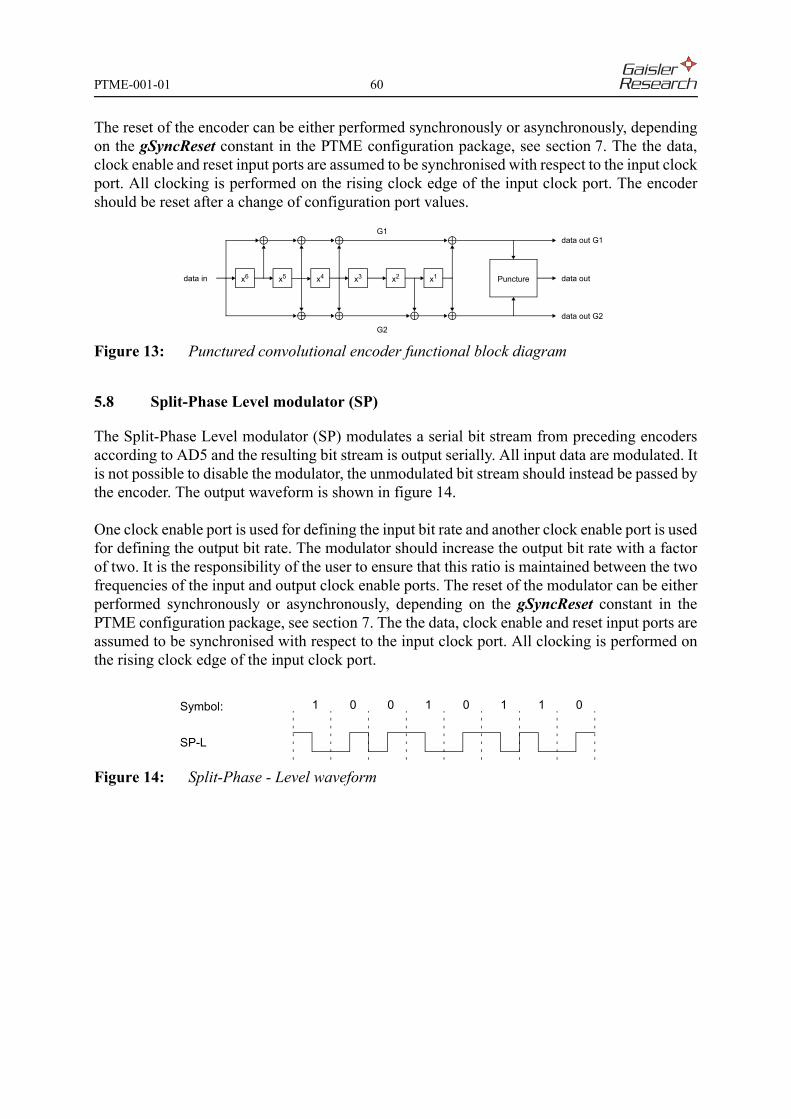
PTME-001-01 60
The reset of the encoder can be either performed synchronously or asynchronously, dependingon the gSyncReset constant in the PTME configuration package, see section 7. The the data,clock enable and reset input ports are assumed to be synchronised with respect to the input clockport. All clocking is performed on the rising clock edge of the input clock port. The encodershould be reset after a change of configuration port values.
Figure 13: Punctured convolutional encoder functional block diagram
5.8 Split-Phase Level modulator (SP)
The Split-Phase Level modulator (SP) modulates a serial bit stream from preceding encodersaccording to AD5 and the resulting bit stream is output serially. All input data are modulated. Itis not possible to disable the modulator, the unmodulated bit stream should instead be passed bythe encoder. The output waveform is shown in figure 14.
One clock enable port is used for defining the input bit rate and another clock enable port is usedfor defining the output bit rate. The modulator should increase the output bit rate with a factorof two. It is the responsibility of the user to ensure that this ratio is maintained between the twofrequencies of the input and output clock enable ports. The reset of the modulator can be eitherperformed synchronously or asynchronously, depending on the gSyncReset constant in thePTME configuration package, see section 7. The the data, clock enable and reset input ports areassumed to be synchronised with respect to the input clock port. All clocking is performed onthe rising clock edge of the input clock port.
Figure 14: Split-Phase - Level waveform
x6 x5 x4 x3 x2 x1data in data out
G1
G2
Puncture
data out G1
data out G2
Symbol:
SP-L
1 1 1 10 0 0 0

PTME-001-01 61
5.9 Clock Divider (CD)
Packet Telemetry Encoder (PTME) has a clocking scheme that is partitioned in multiple clockdomains. The two main domains are the system clock domain and the bit clock domain. Thesystem clock domain is predominantly associated with all functions that communicate with theexternal buffer memory. The bit clock domain is associated with all function directly associatedwith the telemetry and channel coding chain. There are several encoders that are part of both thesystem clock domain and the bit clock domain. There are also several local clock domainsassociated with the different input interfaces, which are kept local to each input. Every suchinput interface is also part of the system clock domain.
Since all telemetry and channel coding is performed in the bit clock domain, using the samePTME input clock, it is necessary to generate clock enable signals to cope with bit ratedifferences between the channel encoders. Each encoder has therefore at least one clock enableinput. Those encoders or modulators that increase the bit rate have two clock enable inputs, onefor the input bit rate and one for the output bit rate. The clock enable inputs are also used forregulating the overall bit rate as will be described later.
The BitClk clock input is used for the bit clock domain. This is an input separated from the Clkclock input used for the system clock domain. The PTME can be configured either to operatewith two separate and independent clock frequencies for the system clock domain and the bitclock domain, or to assume that the two clock inputs are always tied to the same external clocksource without any clock skew difference, using the gCommonClock parameter, see section 7.This is configured at compile time. The former option allows the two clock inputs to be eithergenerated from independent sources or to be tied together, since synchronisation logic betweenthe two clock domains will be permanently generated at compile time. The latter option will notproduce any synchronisation logic and the two inputs will be considered as a common clock.
The bit clock input BitClk can be used either for defining the input clock rate of the encoders,or for defining the output clock rate of the encoders. This is configured at compile time usingthe gClockStyle parameter, see section 7. The former option is only useful for encoders that donot increase the bit rate on their outputs. This includes the Telemetry Encoder (TME), the Reed-Solomon Encoder (RSE), the Pseudo-Randomiser (PSR) and the Non-Return-to-Zero Markencoder (NRZ). It also includes the Convolutional Encoder (CE) when used with the basicconvolutional code which features two dedicated unmultiplexed outputs that need to bemultiplexed outside the PTME. The latter option can be used with all encoders, additionallyincluding the Convolutional Encoder (CE) with both basic and punctured convolutional coding,the Turbo Encoder (TE) and the Split-Phase Level modulator (SP). Note that the output clockrate is that of the output of the last encoder or modulator in a coding chain.
The main task of the Clock Divider (CD) is to generate the different clock enable signals thatare used by the different encoders and modulators. To support an arbitrary choice of encodersand modulators in an encoding scheme, the CD generates four different enable signals in thePTME. The first one is used for the basic telemetry bit rate and is used by the TME and the RSE.The second one is used by the CE for the output frequency and can have one of the followingratios with respect to the first enable signal frequency 2, 3/2, 4/3, 6/5 and 8/7. The third one isused by the TE for the output frequency and can have one of the following ratios with respectto the first enable signal frequency: 2, 3/2, 4/3, 6/5 and 8/7. The fourth one is only used by theSP for the output frequency and is twice the frequency of the modulator input. The PSR and

PTME-001-01 62
NRZ can either use the third one or the first one, depending on whether TE is engaged or not.The enable signal used for the SP input frequency can be the second one if CE is engaged, orthe third one if TE is engaged, or else the first one is used. Support is only provided in a givenconfiguration for those encoders that are implemented in the PTME, see section 7.
The CD is also able to divide the bit rate clock frequency by means of the different clock enablesignals. The clock divider can be sized at compile time to accommodate different degrees ofdivision. The divider can be configured during operation to divide the bit rate clock frequencyfrom 1/1 to 1/2n, where n is the width of the clock divider, using the gClockDepth parameter,see section 7. An example of clock division is shown in table 55, where the clock rate selectionis made with the OutputBitRate input. The resulting frequency is used as the output bit rate ofthe last encoder or modulator in the encoding chain. Note that the bit rate clock is not dividedas such, only the different clock enable signal frequencies are divided.
The bit rate relationship between the encoders and modulators in the PTME is shown in table 56.The output symbol rate, fo, can be obtained by dividing the BitClk input, actually generatingclock enable pulses. Since bit rate generation is based on the output symbol rate, fo, of the lastencoder or modulator used in the encoding chain, the telemetry bit rate, ftme, can vary for thesame fo frequency depending on the used encoding scheme as shown in table 56.
There are two ways of implementing a designing that has to operate on different frequencies:either to use a common clock and to distribute separate enable signals; or to use separate clocksignals with different frequencies derived from a common clock. The former approach is easierto manage since only a single clock is required in the design but it can limit the overallperformance of the system. It is also more power consuming than the latter approach.
The latter approach will give a faster implementation if the slowest part of the design alsohappens to be the one with the critical timing path. However, the latter approach requiresaccurate clock tree design and balancing in order to work properly. The PTME VHDL modelhas been based on the former approach to simplify its use, especially in Field ProgrammableGate Array (FPGA) devices.
OutputBitRate(0:7)
00h 1/101h 1/2... ...
FEh 1/255FFh 1/256
Table 55: Example of bit rate clock division for an n=8 bit wide divider

PTME-001-01 63
As it can be seen from table 56, there will be multicycle paths in some of the modules, due tothe use of clock enable signals, when not operated at the maximum possible frequency. It israther simple to define multicycle paths for a module since each module has one or two clockenable signals. By analysing the clock enable periodicity with respect to the clock frequency onecan set a single multicycle path constraint for each module. However, the multicycle paths willonly be valid for some of the possible encoder and modulator combinations. For example, if theTME is operated at the maximum bit rate there will not be any multicycle paths in that moduleas a result of the code rate differences with respect to other encoders such as the CE, and therewill be no multicycle paths due to output bit rate regulation as done by the CD. As a conclusion,the multicycle paths can only be optimised for in implementations where it is known at compiletime that a particular encoder or modulator will not be operated at the highest possible bit rate.
For advanced user there is always the possibility to modify the PTME hierarchy and build a newclocking scheme based on separate clock signals for the different encoders and modulators. Thisapproach will most certainly be required for ASIC designs in order to produce an optimal result.
When an AMBA AHB interface is implemented in the Telemetry Encoder (TME), the clockdomain of this interface will be the same as the system clock domain and will use the Clk clockinput. There is thus no dedicated AMBA AHB clock and reset interface in the PTME.
The CD synchronises the external asynchronous reset input towards the system clock domainand the bit clock domain. The AMBA APB input interfaces are reset by a separate reset signalthat is assumed to be synchronous with corresponding interface clock. The CD should be resetwhenever a configuration input value is changed. The reset of the two clock enable generatorsand clock divider can be either performed synchronously or asynchronously, depending on thegSyncReset constant in the PTME configuration package, see section 7. All clocking isperformed on the rising clock edge of the clock ports.
The PTME supports a any clock frequency ration between BitClk and Clk, provided that theBitClk frequency is never larger than twice the Clk frequency.
TME
RSE TE
CE CE 1/2 1/3 1/4 1/6
SP SP SP SP SP SP SP SP
TME, ftme fo fo/2 fo/2 fo/4 fo fo/2 fo/2 fo/4 fo/2 fo/4 fo/3 fo/6 fo/4 fo/8 fo/6 fo/12RSE, frse - - - - fo fo/2 fo/4 - - - - - - - -TE, fte - - - - - - - - fo fo/2 fo fo/2 fo fo/2 fo fo/2PSR, fte fo fo/2 fo/2 fo/4 fo fo/2 fo/2 fo/4 fo fo/2 fo fo/2 fo fo/2 fo fo/2NRZ, fnrz fo fo/2 fo/2 fo/4 fo fo/2 fo/2 fo/4 fo fo/2 fo fo/2 fo fo/2 fo fo/2CE, fce - - fo fo/2 - - fo fo/2 - - - - - - - -SP, fsp - fo - fo - fo - fo - fo - fo - fo - fo
Table 56: Bit rates for different encoders based on an obtained output frequency

PTME-001-01 64
5.10 Packet Telemetry Encoder (PTME)
The Packet Telemetry Encoder (PTME) module instantiates all encoder and modulator modulespreviously described. The PTME module propagates all interface signals to the relevantembedded modules, with few signal modifications, allowing a high degree of control andobservability of the embedded encoders and modulators. The PTME module combines theinternal unidirectional data buses of the memory interface to a single bidirectional data businterface. This is also done for the Bandwidth Allocation Table (BAT) interface data bus.
5.10.1 Connectivity
The PTME module provides the interconnection between the different encoders and supports allpermissible coding chains. The symbol output of the last encoder in the coding chain is routedto the output interface of the PTME for which a re-synchronisation of the signal is performed toavoid glitch generation. It facilitates an external telemetry test interface, although notcommissioned, to allow telemetry insertion to the Reed-Solomon Encoder (RSE) and TurboEncoder (TE) while bypassing the Telemetry Encoder (TME). The PTME module distributesthe four clock enable signals from the Clock Divider (CD) to the encoders and modulators toobtain the desired bit rate and the correct bit rate increase. It implements the connectivitybetween the enclosed encoders and modulators as described hereafter.
The output from the Telemetry Encoder (TME) can be connected to:• Reed-Solomon encoder• Pseudo-Randomiser• Non-Return-to-Zero Mark encoder• Convolutional encoder• Split-Phase Level modulator
The input to the Reed-Solomon Encoder (TME) can be connected to:• Telemetry encoder
The output from the Reed-Solomon Encoder (TME) can be connected to:• Pseudo-Randomiser• Non-Return-to-Zero Mark modulator• Convolutional encoder• Split-Phase Level modulator
The input to the Turbo Encoder (TE) can be connected to:• Telemetry encoder
The output from the Turbo Encoder (TE) can be connected to:• Pseud-Randomiser• Split-Phase Level modulator
The input to the Pseudo-Randomiser (PSR) can be connected to:• Telemetry encoder• Reed-Solomon encoder

PTME-001-01 65
The output from the Pseud-Randomiser (PSR) can be connected to:• Non-Return-to-Zero Mark modulator• Convolutional encoder• Split-Phase Level modulator
The input to the Non-Return-to-Zero Mark encoder (NRZ) can be connected to:• Telemetry encoder• Reed-Solomon encoder• Pseudo-Randomiser
The output from the Non-Return-to-Zero Mark encoder (NRZ) can be connected to:• Convolutional encoder• Split-Phase Level modulator
The input to the Convolutional Encoder (CE) can be connected to:• Telemetry encoder• Reed-Solomon encoder• Pseudo-Randomiser• Non-Return-to-Zero Mark encoder
The output from the Convolutional Encoder (CE) can be connected to:• Split-Phase Level modulator
The input to the Split-Phase Level modulator (SP) can be connected to:• Telemetry encoder• Reed-Solomon encoder• Pseudo-Randomiser• Non-Return-to-Zero Mark encoder
Due to the flexibility of the coding chain, it is possible to enable illegal encoder combinations.It is the responsibility of the user not to enable the illegal combinations as listed hereafter:• TE and CE• TE and NRZ• TE and RSE
5.10.2 Limitations
The PTME limits to some extent the capabilities of the encoders and modulators included in themodule, which can be understood from the preceding module descriptions. The implementedclocking scheme in the PTME also limits the overall telemetry bit rate performance of the designsince all encoder and modulators are clocked by the same bit rate clock. In the worst case thetelemetry encoder needs to be clocked up to twelve times faster than required for the telemetryrate in order to be compatible with the turbo encoder and the split-phase modulator. Thislimitation can be overcome if the TME, the TE and SP are all clocked on different clocksderived from the same source maintaining clock edge synchronisation, which is however notimplemented in the PTME. This issue is discussed in detail in section 5.9.

PTME-001-01 66
6 MODULE INTERFACES
The Packet Telemetry Encoder (PTME) is based on internal interface structures for which theuse outside the PTME is not considered. The interfaces are therefore described only briefly.
6.1 Multiple input interfaces
The PTME module implements four different type of input interfaces for packet and datatransfer to the Virtual Channels via the Virtual Channel Interface (VCI) defined in section 6.2.Since it is possible to select any type interface for up to eight possible Virtual Channels, eachinterface type has therefore been copied up to eight times in the PTME port declaration. Itshould be noted that only some of these interfaces will be used, which is configured at compiletime as per section 7.
6.2 Virtual Channel Interface (VCI) definition
The Virtual Channel Interface (VCI) resides between each Virtual Channel Assembler (VCA)and its input interface modules. The actual user input interfaces are placed outside the VCAsince there can be several different types of interfaces and protocols to be implemented. TheVCI is designed to provide all the information required by the VCA for proper data insertioninto Transfer Frames. The VCI is synchronous and independent of the preceding input interfaceimplementation.
The VCI provides the VCA with the following information:• Packet start detected• Packet in progress• Packet end detected• Packet to be held• Packet to be aborted• Data word available • Data word (octet)
The VCI provides the input interface module with the following information:• Interface is busy processing the input data• Space available in external buffer memory for a packet (or segment)
The VCI is only capable of processing one data word at a time. There is no other bufferingcapability on the VCI. Buffering can either be made in the input interface module or in the VCAinternal input buffer.

PTME-001-01 67
6.3 PTME Internal Bus (PIB or PI-bus) definition
The communication between Virtual Channel Buffer (VCB) and the different clients: VirtualChannel Assembler (VCA), Virtual Channel Multiplexer (VCM) and Turbo Encoder (TE); isdone over the PTME Internal Bus (PIB or PI-bus).
Each client requests an access to the external buffer memory by asserting a request signal to theVCB. The VCB will acknowledge the request by a grant signal after which the request from theclient can be released. The request input from the client just granted access will be masked inthe next clock period to allow the client to remove its request not to interpret a single request astwo. At the moment the client asserts its request signal it also drives the corresponding frameand octet pointers to inform the VCB of where in the external buffer memory the relevant dataresides, and whether it is a read or a write access. Note that the VCA can only make writeaccesses and the VCM can only make read accesses. These frame and octet pointer values areallowed to change after the request has been granted by the VCB, allowing the client to generatea new request immediately after the previous one has been granted. The VCB will assert a readysignal when the data transfer has been completed. At the moment the VCB asserts its readysignal it will also drive the data read from the external buffer memory on the PIB, provided thatit is a read access. The write frame and octet pointers are used by the VCB to form the absolutememory address or AHB address.
The VCA has two PBI interfaces, one for nominal write accesses and one for auxiliary accessesfor Frame Data Field Status storage or Idle Source Packet insertion. Nominal and auxiliaryaccess requests can be made in parallel. The VCM can only make read accesses. The TE canonly make a write or a read access at a time.
The PIB can also be implemented with a base address and offset address pair, called physicaladdressing, but this is a non-commissioned compile time option.
6.4 Virtual Channel Request (VCR) definition
The communication between the VCAs and the VCM is done over the Virtual Channel Request(VCR) interface. Each VCA informs the VCM when there is enough data in the external buffermemory to fill the complete Data Field of the Transfer Frame. This is done by a request signalto the VCM which will acknowledge the request by a grant signal after which the request fromthe VCA can be released. At the moment the VCA asserts its request signal it also drives thecorresponding frame pointer value to inform the VCM of where in its external buffer memorythe relevant data resides. This frame pointer value is allowed to change after the request hasbeen granted by the VCM, allowing the VCA to generate a new request immediately after theprevious one has been granted.
The VCM will assert a ready signal when the data contents for a frame has been read out fromthe memory after which the VCA is allowed to write over the memory location with newincoming data. The VCM asserts a poll signal each time a VCA is checked for available data,which can be used for initiating Idle Source Packet insertion in the Virtual Channel, seesection 4.2.5.3.

PTME-001-01 68
7 PTME DESIGN OPTIONS
The Packet Telemetry Encoder (PTME) VHDL model is largely configurable at compile timeby constants defined in a configuration package, PTME_Configuration, allowing the number ofsupported Virtual Channels to be selected, allocation of memory space, enabling or disabling ofencoders etc. The constants from the package are then either propagated to the generics of thesub-modules or used directly in the sub-modules as constants.
The PTME model supports a variety of configuration options which will produce a designtailored to user’s needs. The options listed in table 57 and table 58 can be configured beforesynthesis or compilation of the model.
Parameter Type Interpretation Description
Constants related to the Virtual Channels of the Telemetry Encoder (TME)gNumberOfVCs Natural range 1 to 8 Number of VCsgIdleFrameVC Natural range 0 to 7 Identification of VC to use for Idle Transfer FramesgFlexVCId Natural range 0 to 1 Flexible VC Id allocationConstants related to the memory size and partitioninggMemoryDepth Positive 2^n memory bytes Amount of memory to be shared by all VCsgAreaDepth Positive 2^n memory areas Number of areas into which memory is partitionedgGroupDepth Positive 2^n areas grouped Maximum number of memory areas allowed for any VCgGroupInterface Natural range 0 to 1 automatic / manual external memory area assignmentBandwidth Allocation Table configurationgBatDepth Positive 2^n entire Number of BAT entriesConfiguration of PTME capabilitiesgFrameLength Natural range 0 to 2 223 based, 239 based, bothgAltASM Natural range 0 to 1 Alternate Attached Synchronisation Marker supportgTime Natural range 0 to 1 Time Strobe supportgSecHeader Natural range 0 to 1 Secondary Header supportgOPCF Natural range 0 to 1 OPCF/CLCW supportgOPCFLength Natural range 0 to 2 CLCW data transfer length 16, 32 or bothgOPCFInterface Natural range 0 to 1 TTC-B-01 / synchronous-parallelgFECW Natural range 0 to 1 FECW/CRC supportgBatInterface Natural range 0 to 2 no interface / asynchronous / synchronous-parallelgPreLength Natural +1 default Virtual Channel Multiplexer internal prefetch buffer size gReedSolomon Natural range 0 to 1 Reed-Solomon encoder supportgRSStyle Natural range 0 to 3 flip-flops, latches, external memory, 50/50gUnContiguous Natural range 0 to 1 Uncontiguous CADU supportgTurbo Natural range 0 to 1 Turbo encoder supportgTurboLengthRd Natural Turbo buffer sizegTurboLengthWr Natural Turbo buffer sizegTurboLatency Natural range 0 to 1 Turbo latency optimisation
Table 57: PTME configuration parameters

PTME-001-01 69
gPseudo Natural range 0 to 1 Pseudo-random supportgMark Natural range 0 to 1 NRZ-Mark supportgConvolute Natural range 0 to 3 no support, basic, punctured, both basic and puncturedgSplit Natural range 0 to 1 Split Phase supportClock divider and clocking style configurationgClockDepth Positive 2^n divider Clock divider widthgCommonClock Natural range 0 to 1 Separate / Common - BitClk and ClkgClockStyle Natural range 0 to 1 Input BitClk / Output BitClkgClkFrequency Natural Clock frequency (Hz) for PacketAsynchronous modulegSyncReset Natural range 0 to 1 Asynchronous reset / Synchronous resetgOPCFBitClock Natural range 0 to 1 OPCF using CLCWClk, OPCF using BitClkMemory addressing stylegPhysicalAddress Natural range 0 to 1 Logical pointer support / Physical address supportgPhysicalDepth Positive Physical address widthgMemoryInterface Natural range 0 to 1 AMBA AHB interface, asynchronous memory interfacegWaitStates Natural range 0 to 1 Wait State supportgWaitStateDepth Positive 2^n -1 wait states Maximum number of wait statesgEdacSupport Natural range 0 to 3 no / sequential / parallel implementation / bothgEdacType Natural range 0 to 1 Hamming Code / Cyclic CodegMemoryTest Natural range 0 to 1 Memory test supportDesign optimisation and simplificationgFPGA Natural range 0 to 1 FPGA targetedgSlowVCAExtra Natural range 0 to 1 Slow access support for VCA auxiliary writegSlowVCAWrite Natural range 0 to 1 Slow access support for VCA write gAcknowledgeVCB Natural range 0 to 1 Acknowledge support in VCBgFrameCheck Natural range 0 to 1 Check frame status in VCM
Parameter Type Interpretation Description
Constants related to the individual Virtual Channels of the Telemetry Encoder (TME)gPacket Natural range 0 to 1 Packet supportgIdle Natural range 0 to 1 Idle Source Packet generation supportgReady Natural range 0 to 1 Ready-for-segment signalling supportgEmpty Natural range 0 to 1 Buffer empty signalling supportgAbort Natural range 0 to 1 Abort packet insertion supportgLength Natural +1 default Internal input buffer size for Virtual Channel AssemblergInterface Natural range 0 to 4 PacketWire, PacketAsynchronous, PacketParallel,
AMBA APB (PAPB), no internal interface modulegPAPBDataSize Natural range 1 to 4 8 bits, 16 bits, 24 bits, 32 bitsgGroupSize Natural 2^n memory areas allocated to Virtual Channel
Table 58: PTME configuration parameters (for individual Virtual Channels)
Parameter Type Interpretation Description
Table 57: PTME configuration parameters

PTME-001-01 70
8 PTME INTERFACES
The Packet Telemetry Encoder (PTME) VHDL model interfaces are listed in table 59 anddescribed in the subsequent sections.
Name Type Mode Description Remark
System interfaceReset_N Std_ULogic in Asynchronous resetClk Std_ULogic in System clockBit rate clock interfaceBitClk Std_ULogic in Bit clockMemory allocation interface (non-commissioned)MaxOctetPtrs OctetPtrMatrixType in Max number of octetsMaxFramePtrs FramePtrMatrixType in Max number of framesBaseAreaPtrs AreaPtrMatrixType in Base area pointersBaseAddresses PhysicAddrMatrixType in Base addressesTurboBase PhysicAddrType in Turbo base addressTurboFill TurboOffSetType in Turbo logical fillGeneral configuration interfaceAltASM Std_ULogic in Enable alternate ASMTimeMode Std_Logic_Vector(0 to 3) in Selects time rateFrameLen Std_Logic_Vector(0 to 2) in Selects frame lengthSCId Std_Logic_Vector(0 to 9) in Spacecraft IdIdleFlexVCId VCPtrType in VC Id separate Idle
Transfer Frame channel
IdleSecHeader Std_ULogic in Secondary HeaderIdleSegmentLen Std_Logic_Vector(0 to 1) in Segment Length IdOPCF Std_ULogic in OPCF/CLCW when '1'FECW Std_ULogic in FECW/CRC when '1'ReedSolomon Std_ULogic in Reed-Solomon codingTurbo Std_ULogic in Turbo codingTurboRate Std_Logic_Vector(0 to 1) in Turbo code ratePseudo Std_ULogic in Pseudo-random codingMark Std_ULogic in NRZ-M codingConvolute Std_ULogic in Convolutional codingConvoluteRate Std_Logic_Vector(0 to 2) in Convolutional rateSplit Std_ULogic in Split Phase-L codingEdacEnable Std_ULogic in Enables EDACEdacParallel Std_ULogic in Select parallel EDACWaitStateRd WaitStateType in Read wait statesWaitStateWr WaitStateType in Write wait statesOutputBitRate ClockPtrType in Output bit rate
Table 59: PTME interfaces

PTME-001-01 71
Virtual Channel Assembler configuration interfacesFlexVCId VCPtrMatrixType in Flexible VC IdPollThreshold ThreeMatrixType in Poll count thresholdRdyThreshold TwoMatrixType in VC ready thresholdDynamicFHP OneMatrixType in Enable FHP insertionSecHeader OneMatrixType in Secondary HeaderSync OneMatrixType in Packets / bit streamPktOrder OneMatrixType in Packet order flagSegmentLen TwoMatrixType in Segment Length IdPktVersion OneMatrixType in Idle Packet VersionBaudRate TwoMatrixType in Baud rate selectorIgnorParity OneMatrixType in Ignore parity bitTwoStopBits OneMatrixType in Two stop bitsVirtual Channel Interface (VCI) (non-commissioned)VCIBegin OneMatrixType in Packet start detectVCIActive OneMatrixType in Packet in progressVCIComplete OneMatrixType in Packet end detectVCIHold OneMatrixType in Packet to be heldVCIAbort OneMatrixType in Packet abortedVCIAvailable OneMatrixType in Data availableVCIData OctetMatrixType in Data inputVCIBusy OneMatrixType out Not ready for octetVCIRdy OneMatrixType out Ready for paketVCIEmpty OneMatrixType out No packet in bufferPacketWire input interfacePWValid OneMatrixType in Packet delimiterPWClk OneMatrixType in Bit clockPWData OneMatrixType in DataPWAbort OneMatrixType in Abort packetPWBusy_N OneMatrixType out Not ready for octetPWRdy OneMatrixType out Ready for paketPWEmpty OneMatrixType out No packet in bufferPacketAsynchronous input interfacePAValid_N OneMatrixType in Packet delimiterPAData OneMatrixType in Asynchronous bitPAAbort OneMatrixType in Abort packetPABusy_N OneMatrixType out Not ready for octetPARdy OneMatrixType out Ready for paketPAEmpty OneMatrixType out No packet in buffer
Name Type Mode Description Remark
Table 59: PTME interfaces

PTME-001-01 72
PacketParallel input interfacePPValid_N OneMatrixType in Packet delimiterPPWr_N OneMatrixType in Octet write strobePPData OctetMatrixType in Octet dataPPAbort OneMatrixType in Abort packetPPBusy_N OneMatrixType out Not ready for octetPPRdy OneMatrixType out Ready for paketPPEmpty OneMatrixType out No packet in bufferPacketAPB input interfacePCLK Std_ULogic in Interface clockPRESETn Std_ULogic in Synchronised resetPAPBIn APB_Slv_In_Vector(7 downto 0) in Interface inputPAPBOut APB_Slv_Out_Vector(7 downto 0) out Interface outputPAPBBusy_N OneMatrixType out Not ready for octetPAPBRdy OneMatrixType out Ready for paketPAPBEmpty OneMatrixType out No packet in bufferMemory test interface (non-commissioned)TestReq Std_ULogic in RequestTestRead Std_ULogic in Read accessTestWrite Std_ULogic in Write accessTestGnt Std_ULogic out Access grantedTestRdy Std_ULogic out Access completedTestAddr StdAddrType in AddressTestRdData Octet out Data outputTestWrData Octet in Data inputTestBaseAddr PhysicAddrType in Base addressTestOffset PhysicAddrType in Offset addressMemory interfaceCS_N Std_ULogic out Chip selectRd_N Std_ULogic out Enable data readWr_N Std_ULogic out Enable data writeAddress StdAddrType out AddressData Octet inout DataEDAC interfaceEdac Octet inout Check bitsEdacErr Std_Logic_Vector(0 to 1) out Error codeAMBA AHB Master interfaceAHBMasterIn AHB_Mst_In_Type inAHBMasterOut AHB_Mst_Out_Type outTelemetry test interface (non-commissioned)Test Std_ULogic in test enable
Name Type Mode Description Remark
Table 59: PTME interfaces

PTME-001-01 73
TestIn Std_ULogic in telemetry dataTestSyncIn Std_ULogic in ASM delimiterTestFrameIn Std_ULogic in Frame delimiterTestTurboSync Std_ULogic in Turbo delimiterTestTurboFrame Std_ULogic in Turbo delimiterTestTurboTerm Std_ULogic in Turbo delimiterTestOut Std_ULogic out telemetry dataTestSyncOut Std_ULogic out ASM delimiterTestFrameOut Std_ULogic out Frame delimiterTestBitTick Std_ULogic out bit delimiterChannel Access Data Unit output interfaceTimeStrobe Std_ULogic out Time strobeCADUSyncMark Std_ULogic out ASM delimiterCADUFrameMark Std_ULogic out Frame delimiterCADUOddFrame Std_ULogic out Odd numbered frameCADUClk Std_ULogic out CADU clockCADUOut Std_ULogic out CADU dataCADUG1Out Std_ULogic out Convoluted CADU dataCADUG2Out Std_ULogic out Convoluted CADU dataBandwidth Allocation Table interfaceBatPriority Std_ULogic in Priority VC selectBatRegister BatFileType in Register fileBatWrite Std_ULogic out Allowed to writeBatCS_N Std_ULogic in Chip selectBatRW_N Std_ULogic in Read/writeBatA BatAddressType in AddressBatD BatDataType inout Data input Operation Control Field / CLCW / TTC-B-01 interfaceCLCWLength Std_ULogic in CLCW length selectCLCWData Std_Logic_Vector(0 to 31) in CLCW parallel dataCLCWWrite Std_ULogic out Allowed to writeCLCWOverWrite Std_ULogic in Overwrite bit 16 and 17CLCWNoRFAvail Std_ULogic in Bit 16CLCWNoBitLock Std_ULogic in Bit 17TCId0 Std_Logic_Vector(0 to 5) in TC VC Id no. 0TCId1 Std_Logic_Vector(0 to 5) in TC VC Id no. 1CLCWClk Std_ULogic in CLCW clockCLCWSel Std_ULogic in Selects TTCD0/TTCD1TTCSample Std_ULogic out TTC-B-01 sampleTTCClk Std_ULogic out TTC-B-01 clockTTCD0 Std_ULogic in TTC-B-01 input no. 0TTCD1 Std_ULogic in TTC-B-01 input no. 1
Name Type Mode Description Remark
Table 59: PTME interfaces

PTME-001-01 74
8.1 System interface
8.1.1 Reset_N: Synchronised reset: Std_ULogic (I)
This active low input signal asynchronously resets the PTME VHDL model. The signal isassumed to be asynchronous.
8.1.2 Clk: System clock: Std_ULogic (I)
This input signal is the system clock signal for the PTME VHDL model. Most registers areclocked on the rising Clk edge.
8.2 Bit rate interface
8.2.1 BitClk: Bit clock: Std_ULogic (I)
This is the bit clock used by the various encoders in the PTME. All registers are clocked on therising edge.
8.3 Memory allocation interface
Non-commissioned interface.
8.4 General configuration interface
8.4.1 AltASM: Enable alternate ASM: Std_ULogic (I)
Enables the output of the alternative ASM. Not effective with Turbo Encoding. The PTMEshould be reset after each change.
8.4.2 TimeMode: Time rate selection: Std_Logic_Vector(0 to 3) (I)
Selects the rate of the time strobe periodicity as per table 24. The PTME should be reset aftereach change.
8.4.3 FrameLen: Transfer Frame length selection: Std_Logic_Vector(0 to 2) (I)
Selects the Transfer Frame length as per table 20. The PTME should be reset after each change.
8.4.4 SCId: Spacecraft Identifier: Std_Logic_Vector(0 to 9) (I)
Sets the Spacecraft Identifier. The PTME should be reset after each change.
8.4.5 IdleFlexVCId: Flexible VC Id for Idle Transfer Frames: VCPTRType (I)
Sets the VC Id for Idle Transfer Frames when output on a separate Virtual Channel and inconfiguration flexible allocation is implemented. The PTME should be reset after each change.
8.4.6 IdleSecHeader: Secondary Header for Idle Transfer Frames: Std_ULogic (I)
Enables Secondary Header generation for Idle Transfer Frames when output on a separateVirtual Channel. The PTME should be reset after each change.

PTME-001-01 75
8.4.7 IdleSegmentLen: Segment Length Identifier for Idle Transfer Frames: Std_Logic_Vector(0 to 1) (I)
Data bits in Frame Data Field Status of Idle Transfer Frames when output on a separate VirtualChannel. The PTME should be reset after each change.
8.4.8 OPCF: Operational Control Field enable: Std_ULogic (I)
Enables OPCF generation when asserted. The PTME should be reset after each change.
8.4.9 FECW: Frame Error Control Word enable: Std_ULogic (I)
Enables FECW generation when asserted. The PTME should be reset after each change.
8.4.10 ReedSolomon: Reed-Solomon coding enable: Std_ULogic (I)
Enables Reed-Solomon encoding when asserted. The PTME should be reset after each change.
8.4.11 Turbo: Turbo coding enable: Std_ULogic (I)
Enables Turbo encoding when asserted. The PTME should be reset after each change.
8.4.12 TurboRate: Reed-Solomon coding rate: Std_Logic_Vector(0 to 1) (I)
Selects Turbo code rate as per table 53. The PTME should be reset after each change.
8.4.13 Pseudo: Pseudo-Randomiser enable: Std_ULogic (I)
Enables Pseudo-Randomisation when asserted. The PTME should be reset after each change.
8.4.14 Mark: Non-Return-to-Zero - Mark enable: Std_ULogic (I)
Enables non-return-to-zero - mark encoding when asserted. The PTME should be reset aftereach change.
8.4.15 Convolute: Convolutional encoding enable: Std_ULogic (I)
Enables Convolutional encoding when asserted. The PTME should be reset after each change.
8.4.16 ConvoluteRate: Convolutional coding rate: Std_Logic_Vector(0 to 1) (I)
Selects Convolutional code rate as per table 54. The PTME should be reset after each change.
8.4.17 Split: Split-Phase - Level enable: Std_ULogic (I)
Enables split-phase - level modulation when asserted. The PTME should be reset after eachchange.
8.4.18 EdacEnable: EDAC enable: Std_ULogic (I)
Enables EDAC protection of memory when asserted. Only effective when memory interfaceand EDAC are implemented. The PTME should be reset after each change.

PTME-001-01 76
8.4.19 EdacParallel: Parallel EDAC selection: Std_ULogic (I)
Selects parallel EDAC operation when asserted, else sequential EDAC operation is selected.Only effective when memory interface and EDAC with both parallel and sequential operationare implemented. The PTME should be reset after each change.
8.4.20 WaitStateRd: Wait states for read access: WaitStateType (I)
Sets the number of wait states for a read access. Only effective when memory interface isimplemented with wait state support. The PTME should be reset after each change.
8.4.21 WaitStateWr: Wait states for write access: WaitStateType (I)
Sets the number of wait states for a write access. Only effective when memory interface isimplemented with wait state support. The PTME should be reset after each change.
8.4.22 OutputBitRate: Output bit rate selection: ClockPtrType (I)
Sets the bit rate derived from the system clock for the encoding chain. Only effective when thesystem clock is enabled for symbol rate generation. The PTME should be reset after eachchange.
8.5 Virtual Channel Assembler configuration interfaces
The different Virtual Channels Assemblers are individually configured via this interface. Aninput array of entire is provided for each parameters, being indexed by the Virtual Channelnumber. The description hereafter is based on the type of the array entries rather than the arrayitself.
8.5.1 FlexVCId: Virtual Channel Identifier selection: VCPtrMatrixType (I)
Sets the Virtual Channel Identifier in configuration flexible allocation is implemented. ThePTME should be reset after each change.
8.5.2 PollThreshold: Poll count threshold: Std_Logic_Vector(0 to 2) (I)
Sets the poll threshold for Idle Source Packet insertion, as per table 27. The PTME should bereset after each change.
8.5.3 RdyThreshold: Memory availability threshold: Std_Logic_Vector(0 to 1) (I)
Sets the external buffer memory availability threshold, as per table 26. The PTME should bereset after each change.
8.5.4 DynamicFHP: Dynamic FHP enable: Std_ULogic (I)
Enables dynamic calculation of First Header Pointer when asserted. The PTME should be resetafter each change.
PTME-001-01 77
8.5.5 SecHeader: Secondary Header Flag: Std_ULogic (I)
Enables Secondary Header generation when asserted. The PTME should be reset after eachchange.
8.5.6 Sync: Data Field Synchronisation Flag: Std_ULogic (I)
Indicates whether packets are synchronously inserted, when 0b, or asynchronously inserted,when 1b. Acts as a qualifier for Idle Source Packet generation. The PTME should be reset aftereach change.
8.5.7 PktOrder: Packet Order Flag: Std_ULogic (I)
Data bit in Frame Data Field Status. The PTME should be reset after each change.
8.5.8 SegmentLen: Segment Length Identifier: Std_Logic_Vector(0 to 1) (I)
Data bits in Frame Data Field Status. The PTME should be reset after each change.
8.5.9 PktVersion: Packet Order Flag: Std_ULogic (I)
Data bit in Idle Source Packet, corresponding to bit 0 of the Version Number. The PTME shouldbe reset after each change.
8.5.10 BaudRate: Baud rate selection: Std_Logic_Vector(0 to 1) (I)
Sets the baud rate for the PA interface, as per table 30. The PTME should be reset after eachchange.
8.5.11 IgnorParity: Ignore parity bit: Std_ULogic (I)
When asserted, a parity is included in the received data on the PA interface and should beignored. The PTME should be reset after each change.
8.5.12 TwoStopBits: Two stop bits: Std_ULogic (I)
When asserted, two stop bits received on the PA interface and should be checked for validity.The PTME should be reset after each change.
8.6 Virtual Channel Interface (VCI)
Non-commissioned interface.

PTME-001-01 78
8.7 PacketWire (PW) input interface
The different interfaces are individually interfaced via this interface. An array of entire isprovided for each port, being indexed by the Virtual Channel number. The description hereafteris based on the type of the array entries rather than the array itself. Note that only some of theentries in the array might actually be used in a design.
8.7.1 PWValid: Packet delimiter: Std_ULogic (I)
This input signal is the packet delimiter for the interface. It should be de-asserted betweenpackets.
8.7.2 PWClk: Bit clock: Std_ULogic (I)
This input signal is the PackeWire bit clock. The receiver registers are clocked on the risingPWClk edge.
8.7.3 PWData: Data: Std_ULogic (I)
This input signal is the serial data input for the interface. Data are sampled on the rising PWClkedge when PWValid is asserted.
8.7.4 PWRdy: Ready for paket: Std_ULogic (O)
This signal indicates whether the Virtual Channel is ready to receive one segment. The outputis clocked out on the rising Clk edge.
8.7.5 PWBusy_N: Not ready for data: Std_ULogic (O)
This signal indicates whether the Virtual Channel is ready to receive one octet. The output isclocked out on the rising Clk edge.
8.7.6 PWAbort: Abort paket: Std_ULogic (I)
This signal indicates that a packet should be aborted.
8.7.7 PWEmpty: No packet in buffer: Std_ULogic (O)
This signal indicates whether the Virtual Channel does not contain any user packet data. It canhowever contain idle packet data. The output is clocked out on the rising Clk edge.

PTME-001-01 79
8.8 PacketAsynchronous (PA) input interface
The different interfaces are individually interfaced via this interface. An array of entire isprovided for each port, being indexed by the Virtual Channel number. The description hereafteris based on the type of the array entries rather than the array itself. Note that only some of theentries in the array might actually be used in a design.
8.8.1 PAValid_N: Packet delimiter: Std_ULogic (I)
This input signal is the packet delimiter for the interface. It should be de-asserted betweenpackets. It can also be tied to logic zero if non-packet data is to be transferred.
8.8.2 PAData: Data: Std_ULogic (I)
This input signal is the bit serial asynchronous data input for the interface.
8.8.3 PARdy: Ready for paket: Std_ULogic (O)
This signal indicates whether the Virtual Channel is ready to receive one segment. The outputis clocked out on the rising Clk edge.
8.8.4 PABusy_N: Not ready for data: Std_ULogic (O)
This signal indicates whether the Virtual Channel is ready to receive one octet. The output isclocked out on the rising Clk edge.
8.8.5 PAAbort: Abort paket: Std_ULogic (I)
This signal indicates that a packet should be aborted.
8.8.6 PAEmpty: No packet in buffer: Std_ULogic (O)
This signal indicates whether the Virtual Channel does not contain any user packet data. It canhowever contain idle packet data. The output is clocked out on the rising Clk edge.
8.9 PacketParallel (PP) input interface
The different interfaces are individually interfaced via this interface. An array of entire isprovided for each port, being indexed by the Virtual Channel number. The description hereafteris based on the type of the array entries rather than the array itself. Note that only some of theentries in the array might actually be used in a design.
8.9.1 PPValid_N: Packet delimiter: Std_ULogic (I)
This input signal is the packet delimiter for the interface. It should be de-asserted betweenpackets. It can also be tied to logic zero if non-packet data is to be transferred.
8.9.2 PPData: Data: Octet (I)
This input signal is the 8 bit parallel data input for the interface. It is sampled on the risingPPWr_N edge.

PTME-001-01 80
8.9.3 PPWr_N: Octet write strobe: Std_ULogic (I)
This input signal is the octet write strobe. The data is sampled on the rising PPWr_N edge.
8.9.4 PPRdy: Ready for paket: Std_ULogic (O)
This signal indicates whether the Virtual Channel is ready to receive one segment. The outputis clocked out on the rising Clk edge.
8.9.5 PPBusy_N: Not ready for data: Std_ULogic (O)
This signal indicates whether the Virtual Channel is ready to receive one octet. The output isclocked out on the rising Clk edge.
8.9.6 PPAbort: Abort paket: Std_ULogic (I)
This signal indicates that a packet should be aborted.
8.9.7 PPEmpty: No packet in buffer: Std_ULogic (O)
This signal indicates whether the Virtual Channel does not contain any user packet data. It canhowever contain idle packet data. The output is clocked out on the rising Clk edge.
8.10 PacketAPB (PAPB) input interface
The different interfaces are individually interfaced via this interface. An array of entire isprovided for each port, being indexed by the Virtual Channel number. Note that only some ofthe entries in the array might actually be used in a design. The description hereafter is based onthe type of the array entries rather than the array itself. For detailed information on the recordsused for the APB interface see AD9 and AD12. The clock and reset signals are common for allinterfaces.
8.10.1 PRESETn: Synchronised reset: Std_ULogic (I)
This active low input signal asynchronously resets the AMBA APB interfaces in the PTMEVHDL core. The signal is assumed to be synchronous with the AMBA APB clock PCLK risingedge. The input is used on registers that are all clocked on the rising PCLK edge.
8.10.2 PCLK: Interface clock: Std_ULogic (I)
This input signal is the AMBA APB clock which is the clock for the AMBA APB interfaces inthe PTME VHDL core. All registers are clocked on the rising PCLK edge.
8.10.3 PAPBIn: Interface input: APB_Slv_In_Type (I)
This signal record is the slave interface input.
8.10.3.1 PSEL: Slave select: Std_ULogic (I)
This signal indicates that the APB slave device is selected and a data transfer is required. Theinput is sampled on the rising PCLK edge for write accesses.
PTME-001-01 81
8.10.3.2 PENABLE: Enable strobe: Std_ULogic (I)
This strobe signal is used to time all accesses on the peripheral bus. The enable signal is used toindicate the second cycle of an APB transfer. The rising edge of PENABLE occurs in the middleof the APB transfer. The input is sampled on the rising PCLK edge for write accesses.
8.10.3.3 PADDR: Address bus: Std_Logic_Vector(PAMAX-1 downto 0) (I)
This is the APB address bus can be up to 32 bits wide. The input is sampled on the rising PCLKedge for write accesses. PAMAX is defined in the AMBA VHDL package, AD12.
8.10.3.4 PWRITE: Write strobe: Std_ULogic (I)
This signal indicates the APB transfer direction When asserted this signal indicates an APBwrite access and when de-asserted a read access. The input is sampled on the rising PCLK edge.
8.10.3.5 PWDATA: Write data bus: Std_Logic_Vector(PDMAX-1 downto 0) (I)
The APB write data bus is driven by the peripheral bus master during write cycles (whenPWRITE is asserted). The data is sampled on the rising PCLK edge for write accesses. PDMAXis defined in the AMBA VHDL package, AD12.
8.10.4 PAPBOut: Interface output: APB_Slv_Out_Type (O)
This signal record is the slave interface output.
8.10.4.1 PRDATA: Read data bus: Std_Logic_Vector(PDMAX-1 downto 0) (O)
The APB read data bus is driven by the selected slave during read cycles (when PWRITE is de-asserted). PDMAX is defined in the AMBA VHDL package, AD12.
8.10.5 PAPBRdy: Ready for paket: Std_ULogic (O)
This signal indicates whether the Virtual Channel is ready to receive one segment. The outputis clocked out on the rising Clk edge.
8.10.6 PAPBBusy_N: Not ready for data: Std_ULogic (O)
This signal indicates whether the Virtual Channel is ready to receive one octet. The output isclocked out on the rising Clk edge.
8.10.7 PAPBEmpty: No packet in buffer: Std_ULogic (O)
This signal indicates whether the Virtual Channel does not contain any user packet data. It canhowever contain idle packet data. The output is clocked out on the rising Clk edge.

PTME-001-01 82
8.11 Memory test interface
Non-commissioned interface.
8.12 Memory interface
8.12.1 CS_N: Memory chip select: Std_ULogic (O)
This active low output is the chip select for the external memory. CS_N changes state on therising Clk edge.
8.12.2 Wr_N: Memory write strobe: Std_ULogic (O)
This active low output is the write strobe for the external memory. Wr_N changes state on thefalling Clk edge.
8.12.3 Rd_N: Memory read strobe: Std_ULogic (O)
This active low output is the read strobe for the external memory. Rd_N changes state on therising Clk edge.
8.12.4 Address Memory address: StdAddrType (O)
These outputs are the addresses generated by the PTME for reading and writing to the externalmemory. They change state on the rising Clk edge.
8.12.5 Data: Memory data: Octet (I/O)
These signals are used to read and write data to the external memory. They are driven by thePTME on the rising Clk edge and are tristated on the falling Clk edge.
8.13 EDAC interface
8.13.1 Edac: EDAC check bit data: Octet (I/O)
These signals are used to read and write EDAC check bits to the external memory. They aredriven by the PTME on the rising Clk edge and are tristated on the falling Clk edge.
8.13.2 EdacErr: EDAC error flags: Std_Logic_Vector (0 to 1) (I/O)
These signals are used signal errors detected by the EDAC. They are output on the rising Clkedge.

PTME-001-01 83
8.14 AMBA AHB master interface
For detailed information on the records used for the AMBA AHB interface see AD10 andAD12.
8.14.1 AHBMasterIn: Interface input: AHB_Mst_In_Type (I)
This signal record is the general AHB master interface input.
8.14.1.1 HGRANT: Bus grant: Std_ULogic (I)
This signal indicates that the AHB master device is selected and a data transfer is required. Theinput is sampled on the rising HCLK edge.
8.14.1.2 HREADY: Transfer done: Std_ULogic (I)
This signal indicates to the AHB master device that an access is completed. The input is sampledon the rising HCLK edge.
8.14.1.3 HRESP: Response type: Std_Logic_Vector(1 downto 0) (I)
This signal indicates to the AHB master device with what a result an access has been completed.The input is sampled on the rising HCLK edge.
8.14.1.4 HRDATA: Read data bus: Std_Logic_Vector(HDMAX-1 downto 0) (I)
This signal provides the AHB master device read data at the end of the access. The input issampled on the rising HCLK edge. HDMAX is defined in the AMBA VHDL package, AD12.HDMAX is assumed to be the default 32.
8.14.2 AHBMasterOut: Interface output: AHB_Mst_Out_Type (O)
This signal record is the general AHB master interface output.
8.14.2.1 HBUSREQ: Bus request: Std_ULogic (O)
This signal indicates that the AHB master device is requesting the bus. The output is clockedout on the rising HCLK edge.
8.14.2.2 HLOCK: Lock request: Std_ULogic (O)
This signal indicates whether the AHB master device is requesting a locked access. The outputis permanently driven to logical zero.
8.14.2.3 HTRANS: Transfer type: Std_Logic_Vector(1 downto 0) (O)
This signal indicates the type of the transfer that the AHB master device is issuing. The outputis clocked out on the rising HCLK edge.

PTME-001-01 84
8.14.2.4 HADDR: Transfer type: Std_Logic_Vector(HAMAX-1 downto 0) (O)
This signal carries the address of the transfer that the AHB master device is issuing. The outputis clocked out on the rising HCLK edge. HAMAX is defined in the AMBA VHDL package,AD12. HAMAX is assumed to be the default 32.
8.14.2.5 HWRITE: Read / Write: Std_ULogic (O)
This signal indicates whether it is a read or a write access that the AHB master device is issuing.The output is clocked out on the rising HCLK edge.
8.14.2.6 HSIZE: Transfer size: Std_Logic_Vector(2 downto 0) (O)
This signal indicates the size of the access that the AHB master device is issuing. The output ispermanently driven to logical zeros, indicating a byte access.
8.14.2.7 HBURST: Burst type: Std_Logic_Vector(2 downto 0) (O)
This signal indicates the burst type of access that the AHB master device is issuing. The outputis permanently driven to logical zeros, indicating a single access.
8.14.2.8 HPROT: Protection control: Std_Logic_Vector(32 downto 0) (O)
This signal indicates the protection type of access that the AHB master device is issuing. Theoutput is permanently driven to logical zeros.
8.14.2.9 HWDATA: Write data bus: Std_Logic_Vector(HDMAX-1 downto 0) (O)
This signal carries the data of the write transfer that the AHB master device is issuing. Theoutput is clocked out on the rising HCLK edge. HDMAX is defined in the AMBA VHDLpackage, AD12. HDMAX is assumed to be the default 32. Since only byte accesses areperformed, the byte data to be written is copied to all four byte positions on HWDATA.

PTME-001-01 85
8.15 Telemetry test interface
Non-commissioned interface.
8.16 Channel Access Data Unit output interface
8.16.1 TimeStrobe: Time strobe: Std_ULogic (O)
This signal is asserted when a time strobe is to be generated as specified for Virtual Channel 0.The output is clocked out on the rising BitClk edge.
8.16.2 CADUSyncMark: ASM delimiter: Std_ULogic (O)
This signal is asserted when the Attached Synchronisation Marker is being output. The outputis clocked out on the rising BitClk edge.
8.16.3 CADUFrameMark: Transfer frame delimiter: Std_ULogic (O)
This signal is asserted when the Transfer Frame is being output. The output is clocked out onthe rising BitClk edge.
8.16.4 CADUClk: CADU clock: Std_ULogic (O)
This signal is the bit delimiter for the CADU output. The output is clocked out on the risingBitClk edge.
8.16.5 CADUOut: CADU data: Std_ULogic (O)
This signal is the bit serial CADU data output. The output is clocked out on the rising BitClkedge.
8.16.6 CADUOddFrame: Odd numbered Transfer Frame: Std_ULogic (O)
This signal is asserted when a Transfer Frame for which the Master Channel Frame Count valueis odd. The output is clocked out on the rising BitClk edge.
8.16.7 CADUG1Out: Convoluted CADU data: Std_ULogic (O)
This output carries the G1 data vector from the Convolutional encoder. The output is clockedout on the rising BitClk edge.
8.16.8 CADUG2Out: Convoluted CADU data: Std_ULogic (O)
This output carries the G2 data vector from the Convolutional encoder. The output is clockedout on the rising BitClk edge.

PTME-001-01 86
8.17 Bandwidth Allocation Table interface
8.17.1 BatPriority: Priority mode: Std_ULogic (I)
Enables priority mode when asserted. The PTME should be reset after each change.
8.17.2 BatRegister: Register file: BatFileType (I)
Input of the full BAT register file when the external synchronous interface option is selected.The PTME should be reset if value changes out side the BatWrite window.
8.17.3 BatWrite: Register file write permission: Std_ULogic (O)
Indicates when the register file BatRegister can be modified without the need for a PTME resetwhen the external synchronous interface option is selected.
8.17.4 BatCS_N: Chip select: Std_ULogic (I)
Active low chip select for BAT access when asynchronous interface option is selected.
8.17.5 BatRW_N: Read/Write indicator: Std_ULogic (I)
Active read/write indicator for BAT access when asynchronous interface option is selected.
8.17.6 BatA: Address: BatAddressType (I)
Address for the BAT access when asynchronous interface option is selected.
8.17.7 BatD: Data: BatDataType (I/O)
Data for BAT read and write access when asynchronous interface option is selected.

PTME-001-01 87
8.18 Operation Control Field / CLCW / TTC-B-01 interface
8.18.1 CLCWLength: CLCW data transfer length: Std_ULogic (I)
Indicates the size of the CLCW data word to be transferred. Only used when both 16 and 32 bitCLCW data width support is implemented. The PTME should be reset after each change.
8.18.2 CLCWData: CLCW parallel data: Std_Logic_Vector(0 to 31) (I)
Synchronous parallel CLCW data input when the external synchronous interface option isselected. Should not change out side the CLCWWrite window.
8.18.3 CLCWWrite: CLCW write permission: Std_ULogic (O)
Indicates when CLCWData can be modified when the external synchronous interface is used.
8.18.4 CLCWOverWrite: Overwrite bits 16 and 17: Std_ULogic (I)
Indicates that bit 16 and 17 should be overwritten with the contents of the two following inputs.The PTME should be reset after each change.
8.18.5 CLCWNoRFAvail: No RF Available, bit 16: Std_ULogic (I)
8.18.6 CLCWNoBitLock: No Bit Lock, bit 17: Std_ULogic (I)
8.18.7 TCId0: Virtual Channel Identifier setting: Std_Logic_Vector(0 to 5) (I)
Virtual Channel Identifier setting for CLCW transmitted while CLCWSel is asserted.
8.18.8 TCId1: Virtual Channel Identifier setting: Std_Logic_Vector(0 to 5) (I)
Virtual Channel Identifier setting for CLCW transmitted while CLCWSel is de-asserted.
8.18.9 CLCWClk: Clock: Std_ULogic (I)
Clock input used for generation of TTC-B-01 protocol.
8.18.10 CLCWSel: CLCW selection: Std_ULogic (I)
Selection between TCId0/TTCD0 or TCId1/TTCD1 transmission as part of the CLCW.
8.18.11 TTCSample: Packet delimiter: Std_ULogic (O)
This signal is the packet delimiter for the interface.
8.18.12 TTCClk: Bit clock: Std_ULogic (O)
This signal is the bit clock for the interface. The data are sampled on the rising TTCClk edge.
8.18.13 TTCD0: Data: Std_ULogic (I)
Data sampled on the rising TTCClk edge when CLCWSel is de-asserted.
8.18.14 TTCD1: Data: Std_ULogic (I)
Data sampled on the rising TTCClk edge when CLCWSel is asserted.

PTME-001-01 88
9 PTME VHDL SOURCE CODE DESCRIPTION
The Packet Telemetry Encoder (PTME) model is written in synthesizable VHDL, currentlytargeted towards the Synplify synthesis tool from Synplicity, but is also compatible with theSynopsys Design Compiler. The PTME is an almost fully synchronous design based on a singlesystem clock strategy. The asynchronous part is related to the different interfaces of the core,such as the PacketWire (PW) input interface. The model and test benches are written accordingto RD4 as far as applicable. The VHDL code complies to VHDL’93, RD5.
9.1 Packages and libraries, interface port and generic types
The following VHDL packages are used in the PTME VHDL model:• Std.Standard, • IEEE.Std_Logic_1164, IEEE.Std_Logic_Arith• AMBA_Lib.AMBA• PTME_Lib.PTME_Configuration, PTME_Lib.PTME_Definition
The PTME VHDL model interfaces does not comply to the normally required Std_ULogic andStd_Logic_Vector types, RD4, since it often uses the UnSigned array type.
The recommended target library for the PTME VHDL model is PTME_Lib. Note that theAMBA interface can be located in another library than AMBA_Lib, but this will require amodification of the PTME VHDL code.
There are no generics used for the top entity in the PTME VHDL model.
9.2 Compilation order
The compilation order for the PTME is as follows:• AMBA_Lib: amba.vhd• PTME_Lib: ptme_lib.vhd
The compilation order for the PTME test bench is as follows:• CCSDS_Lib: ccsds_lib.vhd• PTME_TB_Lib: ptme_tb.vhd
9.3 Simulation
A testbench is provided with the PTME VHDL model which can be used to set up verificationruns. The output from the simulation is in ASCII text format and can be processed off line toverify the Reed-Solomon encoder, the Turbo encoder and the telemetry encoder. The testbenchis configured with the same configuration package as the PTME VHDL model. The testbenchwill adapt itself to the selected PTME configuration.

PTME-001-01 89
9.4 Model hierarchy
The PTME VHDL model hierarchy is listed in table 60.
PTME_Configuration (package)PTME_Definition (package)PacketTelemetryEncoder (PTME)
VirtualChannelEncoder (VCE) Telemetry Encoder(TME)VirtualChannelAssembler (VCA)
VirtualChannelMultiplexer (VCM)VirtualChannelBuffer (VCB)
PacketAsynchronous (PA)PacketAPB (PAPB)PacketParallel (PP)PacketWire (PW)TurboEncoder (TE)
Turbo_ControlTurbo_ConstituentEncodersTurbo_InterleaverTurbo_Table
RS_Package (package)ReedSolomonEncoder (RSE)
RS_AdderRS_CtrlRS_MultiplierRS_SerialShiftRS_Memory
RS_MemoryBlockRS_MemoryLatch
PseudoRandomiser (PSR)ConvolutionalEncoder (CE)NonReturnZero (NRZ)SplitPhase (SP)ClockDivider (CD)
Table 60: PTME VHDL model hierarchy

PTME-001-01 90
APPENDIX A: THEORETICAL BACKGROUND ON REED-SOLOMON CODING
This appendix is based on the textbooks RD11 and RD12, and on the ESA and CCSDSstandards AD3 and AD4, respectively.
A.1 Reference documents
RD11 Error-Control Coding for Computer Systems, T. Rao et al., Prentice-Hall International,1989, USA
RD12 Coded-Modulation Techniques for Fading Channels, S. Jamil et al., Kluwer AcademicPublishers, 1994, USA
A.2 Reed-Solomon encoding
Cyclic codes are linear codes having the property that for a given code any cyclic shift of acodeword is also a codeword. Cyclic codes are characterised by using a polynomialrepresentation for codewords and manipulation of polynomials for encoding and decodingprocedures.
An (n, k) cyclic code has the length n of which k symbols are information symbols.
A codeword polynomial of such a code can be represented as
where
Polynomial a(x) is called the information polynomial and is of degree k-1 or less correspondingto the k information symbols ak-1, ak-2, ..., a1, a0, to be encoded.
Polynomial c(x) is called the codeword polynomial and is of degree n-1, corresponding to theencoded information polynomial.
The variable x is a dummy variable only used for indicating the strength or the position of thecorresponding coefficients.
Polynomial g(x) is called the generator polynomial and is of degree r = n-1. The generatorpolynomial has two properties: its coefficients g0 and gr are always non zero; and it dividesxn+1. Using a polynomial of degree n-k which is a factor of xn+1 we can generate an (n, k)cyclic code.
Bose-Chaudhuri-Hocquenghem (BCH) codes are a subclass of cyclic codes, where the symbolsare chosen from a Galois field GF(q), with the generator polynomial having roots in GF(qm*),an extension field of GF(q).
c x( ) a x( ) g x( )⋅=
c x( ) cn 1– xn 1– cn 2– xn 2– ... c1x c0+ + + +=
a x( ) ak 1– xk 1– ak 2– xk 2– ... a1x a0+ + + +=
g x( ) grxr gr 1– xr 1– ... g1x g0+ + + +=

PTME-001-01 91
Reed-Solomon codes are a subclass of BCH codes, where GF(q) and GF(qm*) are chosen to bethe same. The rest of the discussion will be restricted to Reed-Solomon codes with symbolsfrom GF(2m). More on operations in GF(2m) can be found in appendix A.3.
An (n, k) primitive Reed-Solomon code defined over GF(2m) has a code length of n = 2m-1 anda minimum Hamming distance of n-k+1. The number of symbols is n and the number of checksymbols is n-k. The minimum Hamming distance is dmin = n-k+1. A code can correct anycombination of t errors and detect up to d errors (d ≥ t) if and only if dmin ≥ t+d+1. Each symbolis an element of GF(2m).
The generator polynomial of a Reed-Solomon code can be constructed as the least commonmultiple of the minimal polynomials of n-k consecutive powers of the primitive elements ofGF(2m), i.e. αh, αh+1, ..., αh+n-k+1, where h is an integer. This means that the generatorpolynomial of a Reed-Solomon code can be written as
With different values of h, h different generator polynomials can be formed. For
with odd k, g(x) is a self-reciprocal polynomial, i.e.
A self-reciprocal generator polynomial has its coefficients satisfying the following relation
Using self-reciprocal generator polynomials will reduce the number of calculations to beperformed in a Reed-Solomon encoder.
The previous definition of the codeword polynomial calculation for an information polynomialforms a non-systematic codeword, i.e. the information and check symbols are mixed, making itdifficult to extract the information symbols. One can however construct a codeword where thefirst part contains the information symbols and the last part contains the check symbols,according to the following transformations. It shall be noted that a codeword must contain thegenerator polynomial g(x) as a factor.
Let us multiply the information polynomial a(x) with xn-k. A division of a(x)xn-k with g(x)results in the quotient q(x) and the reminder r(x)
g x( ) x αh 1++( )i 0=
n k– 1–
∏ gjxj
j 0=
n k–
∑= =
h k 1+( ) 2⁄=
g x( ) xn k– g 1x--- =
gj gn k– j–=
a x( )xn k–
g x( )---------------------- q x( ) r x( )
g x( )----------+=

PTME-001-01 92
which can be rewritten as
and finally rewritten as
where q(x) is of degree k-1, and r(x) is per definition of one degree less than g(x) which is r-1= n-k-1. The reminder r(x) can be represented as
The codeword of a dummy information polynomial q(x) is according to previous definitions
where c(x) is indeed a factor of g(x). It can also be seen that the first part of the codewordcontains the information symbols and the last part the check symbols
The remainder polynomial r(x) of the division a(x)/g(x) can be calculated using the LinearFeedback Shift Register in figure 15, characterised by the equation
which with r = n-k implements the desired encoder. Note that all additions and multiplicationsof symbols are made in GF(2m).
Figure 15: Codeword polynomial generator
a x( )xn k– q x( )g x( ) r x( )+=
a x( )xn k– r x( )+ q x( )g x( )=
r x( ) a x( )xn k– modg x( ) rixi
i 0=
r 1–
∑ rixi
i 0=
n k– 1–
∑= = =
c x( ) q x( )g x( ) a x( )xn k– r x( )+= =
c x( ) a x( )xn k– r x( )+ cixi
i n k–=
n 1–
∑ cixi
i 0=
n k– 1–
∑+ aixn k– i+
i 0=
k 1–
∑ rixi
i 0=
r 1–
∑+= = =
xrmodg x( ) gr 1– xr 1– gr 2– xr 2– ... g1x x0+ + + +=
1 x xr-1
ss’
01
a(x)
c(x) = a(x)xn-k+r(x)
g0 g1 gr-1

PTME-001-01 93
A.3 Galois fields
A finite Galois field GF(2) contains two elements 0 and 1. The two operations addition andmultiplication are defined as:
The element 0 and 1 are the additive identity and the multiplicative identity elements of GF(2),respectively. A polynomial of degree m defined over GF(2) is represented as
where fi’s are elements in GF(2), i.e., fi = 0 or 1. A polynomial f(x) of degree m with coefficientsin GF(2) is said to be irreducible if it is not divisible by any polynomial with coefficients inGF(2) of degree less than m and greater than zero.
The finite field GF(2m) is an extension of GF(2) generated from and irreducible polynomial f(x)of degree m over GF(2). Equivalently, GF(2) is a subfield of GF(2m), i.e., the elements of GF(2)are also elements of GF(2m). The finite field GF(2m) also has its primitive element α which isthe (2m-1)th root of unity, that is
The finite field GF(2m) contains 2m elements: 0, 1, α, α2, ..., α(2**m-2). The irreduciblepolynomial f(x) of degree m over GF(2) has no roots in GF(2) but its roots lie in some extensionfield of GF(2). If f(x) has the primitive element α of GF(2m) as a root, then it is called a primitiveirreducible polynomial. In this case, αi with i ≤ m can be represented in term of 1, α, α2, ..., αm-1, by using the fact that αi is also a root of f(x), that is
An arbitrary element β of GF(2m) can be represented as a binary m-tuple
Addition Multiplication
+ 0 1 * 0 1
0 0 1 0 0 0
1 1 0 1 0 1
f x( ) fixi
i 0=
m
∑=
α 2m 1–( ) 1=
f αi( ) 0=
β βm 1– βm 2– ... β1 β0, , , ,( )=

PTME-001-01 94
In this case, the zero element is represented as 0 = (0, 0,..., 0). For 0 ≤ i ≤ (m-1), the binarycomponents of the m-tuple representing β = αi satisfy the following relation
Let β and γ be two arbitrary elements of GF(2m) represented in terms of the primitive elementα and binary m-tuples as
Addition in GF(2m) is defined as
where
Multiplication in GF(2m) is defined as
The logical implementation of the addition is straightforward, since the bit wise + operator canbe implemented as an xor-gate. Note that subtraction is identical to addition. The logicalimplementation of the multiplication is somewhat more complicated. Lets start with a look atthe polynomial representation of the multiplication
βj1 ifj, i=
0 elsewhere,
= for j 0 1 ... m 1–( ), , ,{ }=
β αi βm 1– βm 2– ... β1 β0, , , ,( )= =
γ αj γm 1– γm 2– ... γ1 γ0, , , ,( )= =
β γ+ θ θm 1– θm 2– ... θ1 θ0, , , ,( )= =
θi βi γi+= for i 0 1 ... m 1–( ), , ,{ }=
β 0⋅ 0=β 1⋅ β=
β γ⋅ θ αi αj⋅ α i j+( )mod 2m 1–( )= = =
β γ⋅ θ βm 1– xm 1– ,..., β1x β0+ + +( ) γm 1– xm 1– ,..., γ1x γ0+ + +( )⋅= =

PTME-001-01 95
The result of the expansion of this expression for degree m = 8 can be represented as a matrix
where the top row contains the coefficient of x14 being c14 = β7γ7, the next row contains thecoefficient of x13 being c13 = (β7γ6+β6γ7), and so on down to the coefficient of x0 being c0 =β0γ0. The powers from 8 to 14 of x (i.e. m to m-1+m-1) can be expressed in powers of x rangingfrom 0 to 7 (i.e. 0 to m-1) according to a mapping as defined by the field polynomial f(x) ofdegree m defining the Galois field. This can be achieved by simple matrix manipulation. Firstwe collapse the upper part of the matrix to a vector for which each element is the sum si of theelements in the corresponding row of the matrix
β γ⋅
β7γ7 0 0 0 0 0 0 0
β7γ6 β6γ7 0 0 0 0 0 0
β7γ5 β6γ6 β5γ7 0 0 0 0 0
β7γ4 β6γ5 β5γ6 β4γ7 0 0 0 0
β7γ3 β6γ4 β5γ5 β4γ6 β3γ7 0 0 0
β7γ2 β6γ3 β5γ4 β4γ5 β3γ6 β2γ7 0 0
β7γ1 β6γ2 β5γ3 β4γ4 β3γ5 β2γ6 β1γ7 0
β7γ0 β6γ1 β5γ2 β4γ3 β3γ4 β2γ5 β1γ6 β0γ7
0 β6γ0 β5γ1 β4γ2 β3γ3 β2γ4 β1γ5 β0γ6
0 0 β5γ0 β4γ1 β3γ2 β2γ3 β1γ4 β0γ5
0 0 0 β4γ0 β3γ1 β2γ2 β1γ3 β0γ4
0 0 0 0 β3γ0 β2γ1 β1γ2 β0γ3
0 0 0 0 0 β2γ0 β1γ1 β0γ2
0 0 0 0 0 0 β1γ0 β0γ1
0 0 0 0 0 0 0 β0γ0
⇔
β7γ7( )
β7γ6 β6γ7+( )
β7γ5 β6γ6 β5γ7+ +( )
β7γ4 β6γ5 β5γ6 β4γ7+ + +( )
β7γ3 β6γ4 β5γ5 β4γ6 β3γ7+ + + +( )
β7γ2 β6γ3 β5γ4 β4γ5 β3γ6 β2γ7+ + + + +( )
β7γ1 β6γ2 β5γ3 β4γ4 β3γ5 β2γ6 β1γ7+ + + + + +( )
s14
s13
s12
s11
s10
s9
s8
=

PTME-001-01 96
A matrix corresponding to the coefficients of α8 to α14 (i.e. αm to α2m-2) for the fieldpolynomial f(x) is shown here
By multiplying the vector containing the sums si as a scalar to the corresponding row elementsof the matrix containing the coefficients α8 to α14 of the field polynomial f(x), the followingmatrix is obtained
This matrix is then concatenated with the lower part of the matrix containing the expansion ofthe multiplication of the two polynomials β and γ, which results in a final matrix where the sumof each row corresponds to the coefficients (θm-1, ..., θ0) of the product between β and γ
Multiplication with a constant in a fixed Galois field is somewhat more simple and is used inthe calculation of the reminder as explained for Reed-Solomon codes. Assume that β is thevariable and γ is the constant to be multiplied with. By collapsing the matrix above and factoringout β, the following matrix can be obtained. The vector containing β is multiplied as a scalar to
f α14( ) ... f α8( ), ,{ }
f147f146
f145f144
f143f142
f141f140
f137f136
f135f134
f133f132
f131f130
f127f126
f125f124
f123f122
f121f120
f117f116
f115f114
f113f112
f111f110
f107f106
f105f104
f103f102
f101f100
f97f96
f95f94
f93f92
f91f90
f87f86
f85f84
f83f82
f81f80
⇔
s14
s13
s12
s11
s10
s9
s8
f147f137
f127f117
f107f97
f87
f146f136
f126f116
f106f96
f86
f145f135
f125f115
f105f95
f85
f144f134
f124f114
f104f94
f84
f143f133
f123f113
f103f93
f83
f142f132
f122f112
f102f92
f82
f141f131
f121f111
f101f91
f81
f140f130
f120f110
f100f90
f80
f147s14 f137
s13 f127s12 f117
s11 f107s10 f97
s9 f87s8
f146s14 f136
s13 f126s12 f116
s11 f106s10 f96
s9 f86s8
f145s14 f135
s13 f125s12 f115
s11 f105s10 f95
s9 f85s8
f144s14 f134
s13 f124s12 f114
s11 f104s10 f94
s9 f84s8
f143s14 f133
s13 f123s12 f113
s11 f103s10 f93
s9 f83s8
f142s14 f132
s13 f122s12 f112
s11 f102s10 f92
s9 f82s8
f141s14 f131
s13 f121s12 f111
s11 f101s10 f91
s9 f81s8
f140s14 f130
s13 f120s12 f110
s11 f100s10 f90
s9 f80s8
⇒»
f147s14 f137
s13 f127s12 f117
s11 f107s10 f97
s9 f87s8 β7γ0 β6γ1 β5γ2 β4γ3 β3γ4 β2γ5 β1γ6 β0γ7
f146s14 f136
s13 f126s12 f116
s11 f106s10 f96
s9 f86s8 0 β6γ0 β5γ1 β4γ2 β3γ3 β2γ4 β1γ5 β0γ6
f145s14 f135
s13 f125s12 f115
s11 f105s10 f95
s9 f85s8 0 0 β5γ0 β4γ1 β3γ2 β2γ3 β1γ4 β0γ5
f144s14 f134
s13 f124s12 f114
s11 f104s10 f94
s9 f84s8 0 0 0 β4γ0 β3γ1 β2γ2 β1γ3 β0γ4
f143s14 f133
s13 f123s12 f113
s11 f103s10 f93
s9 f83s8 0 0 0 0 β3γ0 β2γ1 β1γ2 β0γ3
f142s14 f132
s13 f122s12 f112
s11 f102s10 f92
s9 f82s8 0 0 0 0 0 β2γ0 β1γ1 β0γ2
f141s14 f131
s13 f121s12 f111
s11 f101s10 f91
s9 f81s8 0 0 0 0 0 0 β1γ0 β0γ1
f140s14 f130
s13 f120s12 f110
s11 f100s10 f90
s9 f80s8 0 0 0 0 0 0 0 β0γ0
θ7
θ6
θ5
θ4
θ3
θ2
θ1
θ0
⇒

PTME-001-01 97
the corresponding row elements of the matrix, which results in a final matrix where the sum ofeach row corresponds to the coefficients (θm-1, ..., θ0) of the product between β and γ
β7
β6
β5
β4
β3
β2
β1
β0
f γα7( )7 f γα7( )6 f γα7( )5 f γα7( )4 f γα7( )3 f γα7( )2 f γα7( )1 f γα7( )0
f γα6( )7 f γα6( )6 f γα6( )5 f γα6( )4 f γα6( )3 f γα6( )2 f γα6( )1 f γα6( )0
f γα5( )7 f γα5( )6 f γα5( )5 f γα5( )4 f γα5( )3 f γα5( )2 f γα5( )1 f γα5( )0
f γα4( )7 f γα4( )6 f γα4( )5 f γα4( )4 f γα4( )3 f γα4( )2 f γα4( )1 f γα4( )0
f γα3( )7 f γα3( )6 f γα3( )5 f γα3( )4 f γα3( )3 f γα3( )2 f γα3( )1 f γα3( )0
f γα2( )7 f γα2( )6 f γα2( )5 f γα2( )4 f γα2( )3 f γα2( )2 f γα2( )1 f γα2( )0
f γα( )7 f γα( )6 f γα( )5 f γα( )4 f γα( )3 f γα( )2 f γα( )1 f γα( )0
f γ( )7 f γ( )6 f γ( )5 f γ( )4 f γ( )3 f γ( )2 f γ( )1 f γ( )0
θ7
θ6
θ5
θ4
θ3
θ2
θ1
θ0
⇒»

PTME-001-01 98
A.4 Derivation of ESA standard from CCSDS recommendation
Since the definition of the (255, 223) Reed-Solomon code differs between the ESA standard,AD3, and the CCSDS recommendation, AD4, a theoretical derivation of the ESA standard fromthe CCSDS recommendation is performed hereafter, showing the required equivalence.
A.4.1 CCSDS standard
The field polynomial in AD4 is specified as
The generator polynomial, in the case of E=16, in AD4 is specified as
Where n = 255, k = 223 and h = 112 results in a self-reciprocal generator polynomial
By expanding the generator polynomial the following coefficients are obtained:
Coefficients of gccsds(x) Polynomial in αccsds
g0 = g32 α0
g1 = g31 α249
g2 = g30 α59
g3 = g29 = g13 = g19 α66
g4 = g28 α4
g5 = g27 α43
g6 = g26 α126
g7 = g25 α251
g8 = g24 α97
g9 = g23 α30
g10 = g22 α3
g11 = g21 α213
g12 = g20 α50
g14 = g18 α170
g15 = g17 α5
g16 α24
Table 61: Coefficients of the generator polynomial gccsds(x) as per AD4
fccsds x( ) x8 x7 x2 x 1+ + + +=
gccsds x( ) x α11j–( )i 112=
143
∏ gj xj⋅j 0=
32
∑= =
h k 1+( ) 2⁄ 112⇒ 223 1+( ) 2⁄= =

PTME-001-01 99
The input and output data from the decoder shall be in the dual basis representation as per AD4where ι0 is transmitted first. Note that the order has been reversed compared to the GFrepresentation otherwise used in this text. Note also that this new representation is the dual basisto a basis βccsds, with the relation βccsds = αccsds
117. The following transformation matrix Tccsdsspecifies the new basis
The following matrix T-1ccsds specifies the revers transformation
A.4.2 ESA standard
The field polynomial in AD3 is specified as
The generator polynomial in AD3 is specified as
Powers of the primitive element α are roots in the ESA generator polynomial gesa(x), whereaspowers of the eleventh power of the primitive element α, i.e. α11, is used in CCSDS generatorpolynomial gccsds(x). To obtain the same generator polynomial for the CCSDS and ESAstandards the relationship between the field polynomials fesa(x) and fccsds(x) should be αesa =αccsds
11.
ι0 ι1 ι2 ι3 ι4 ι5 ι6 ι7 α7 α6 α5 α4 α3 α2 α1 α0
1 0 0 0 1 1 0 11 1 1 0 1 1 1 11 1 1 0 1 1 0 01 0 0 0 0 1 1 01 1 1 1 1 0 1 01 0 0 1 1 0 0 11 0 1 0 1 1 1 10 1 1 1 1 0 1 1
×=
α7 α6 α5 α4 α3 α2 α1 α0 ι0 ι1 ι2 ι3 ι4 ι5 ι6 ι7=
1 1 0 0 0 1 0 10 1 0 0 0 0 1 00 0 1 0 1 1 1 01 1 1 1 1 1 0 11 1 1 1 0 0 0 00 1 1 1 1 0 0 11 0 1 0 1 1 0 01 1 0 0 1 1 0 0
×
fesa x( ) x8 x6 x4 x3 x2 x 1+ + + + + +=
gesa x( ) x αi+( )i 112=
143
∏ gj xj⋅j 0=
32
∑= =

PTME-001-01 100
It can be shown that this relation is indeed valid for the two polynomials. By assuming for amoment that the ESA polynomial fesa(x) is unknown, the following can be deduced from theabove relation. For the powers 0 to 7 of αesa we know the corresponding 8-tuple by thedefinition of a Galois field, as shown in table 62.
We also know the 8-tuples for the powers 0, 11, 22, .., 77 of αccsds since we know the fieldpolynomial fccsds(x). From table 62 it can be deduced that an ESA 8-tuple can be formed froma CCSDS 8-tuple according to the equations in table 63. Since the coefficients of α8 in GF(28)define the corresponding field polynomial, the polynomial fesa(x) can be obtained by insertingαccsds
88 = (0, 1, 0, 0, 0, 0, 1, 0) (which corresponds to αesa8) in to table 63 and solve the resulting
equation system, as done in the ten steps shown in table 64 and table 65.
αesapowers of αesa
α7α6α5α4α3α2α1α0 αccsdspowers of αccsds
α7α6α5α4α3α2α1α0
α0 00000001 α0 00000001
α1 00000010 α11 10101101
α2 00000100 α22 10111110
α3 00001000 α33 00111010
α4 00010000 α44 00111100
α5 00100000 α55 11011100
α6 01000000 α66 01010110
α7 10000000 α77 11001010
Table 62: Relationship between αesa and αccsds
Polynomial in fccsds(x) Coefficients of polynomial in fesa(x)
x0 = x1+x0
x1 = x7+x6+x3+x2
x2 = x6+x5+x4+x2+x1
x3 = x7+x5+x4+x3+x2+x1
x4 = x6+x5+x4+x3+x2+x1
x5 = x4+x3+x2+x1
x6 = x7+x6+x5
x7 = x7+x5+x2+x1
Table 63: Forming an fesa(x) 8-tuple from an fccsds(x) 8-tuple

PTME-001-01 101
The resulting polynomial fitting the equations in table 63 is
which is indeed equivalent to the field polynomial fesa(x) as defined in AD3.
Polynomial in
fccsds
Coefficients of polynomial
in fesa(x)Step 1 Step 2 Step 3 Step 4
0 = x0 x1+x0 x0=x1
1= x1 x7+x6+x3+x2 1=x5+1+x3+x0
0 = x2 x6+x5+x4+x2+x1 0=1+x5+x3
0 = x3 x7+x5+(x4+x3+x2+x1) x5=x7
0 = x4 x6+x5+x4+x3+x2 0=1+x5+x0
0 = x5 x4+x3+x2+x1 x3=x4
1 = x6 x7+x6+x5 x6 = 1
0 = x7 x7+x5+x2+x1 x0=x1=x2
Table 64: Derivation of fesa(x) by solving the equation system for fesa(α8)
Step 5 Step 6 Step 7 Step 8 Step 9 fesa(α8)
1=x5+1+x3+x0 0=x5+x3+x0 0=x5+x5+1+x5+1 x5=0 x7=0 x0=1
0=1+x5+x3 x3=x5+1 x3=1 x4=1 x1=1
0=1+x5+x0 x0=x5+1 x0=1 x1=x2=1 x2=1
x3=1
x4=1
x5=0
x6=1
x7=0
Table 65: Continued derivation of fesa(x)
f x( ) x8 x6 x4 x3 x2 x 1+ + + + + +=

PTME-001-01 102
By expanding the generator polynomial previously defined the following constants are obtained
Each coefficient of the generator polynomial gesa(x) is expressed in powers of αesa and also inpowers of αccsds following the relations αesa = αccsds
11. Note that the coefficients expressed inαccsds are the same as for gccsds(x).
The input and output data from the decoder shall be in the basis representation as per AD3 whereι0 is transmitted first. Note that the order has been reversed compared to the GF(28)representation otherwise used in this text. The following transformation matrix Tesa specifiesthe new basis
Coefficients of gesa(x) Polynomial in αesa Polynomial in αccsds
g0 = g32 α0 α0
g1 = g31 α69 α249
g2 = g30 α214 α59
g3 = g29 = g13 = g19 α6 α66
g4 = g28 α209 α4
g5 = g27 α143 α43
g6 = g26 α81 α126
g7 = g25 α46 α251
g8 = g24 α32 α97
g9 = g23 α165 α30
g10 = g22 α93 α3
g11 = g21 α228 α213
g12 = g20 α190 α50
g14 = g18 α85 α170
g15 = g17 α70 α5
g16 α234 α24
Table 66: Coefficients of the generator polynomial gesa(x) as per AD3
ι0 ι1 ι2 ι3 ι4 ι5 ι6 ι7 α7 α6 α5 α4 α3 α2 α1 α0
0 0 1 1 0 1 1 10 1 0 1 1 1 1 11 0 0 0 0 1 1 10 0 0 0 1 0 0 10 0 1 1 1 1 1 10 0 1 0 1 0 1 10 1 1 1 1 0 0 10 1 1 1 1 0 1 1
×=

PTME-001-01 103
The following matrix T-1esa specifies the revers transformation
By applying all elements of GF(28) over fesa(x) to the above transformation matrix, and then dothe same for all elements of GF(28) over fccsds(x) to the previously defined transformationmatrix, one can easily observe that the two standards map input and output data to the elementsof GF(28)esa and GF(28)ccsds consistently with the αesa = αccsds
11 relation.
Finally, both standards form a generator polynomial g(x) with equivalent coefficients, bothstandards map to the same input and output data. It is therefore reasonable to believe that bothstandards specify the same Reed-Solomon encoder.
The specified Reed-Solomon code can correct up to 16 symbol errors (= t) and detect up to 16errors (= d), since dmin = n-k+1, where dmin = 33, n = 255 and k = 223, and the two relations dmin≥ t+d+1 and d ≥ t both hold.
A.5 Parallel multiplication in dual basis
The reason for employing the conversion to the dual basis as has been shown earlier is that a bitserial multiplier which uses few discrete components can be used, as per AD4. However, thisbit serial multiplier is protected by the patent RD8 which would pose restrictions on anyimplementation using it. Instead, a parallel multiplier can be developed which is suitable forVLSI design having a modest gate count.
Based on the circuitry for generating the reminder polynomial shown in figure 15, astraightforward implementation of a Reed-Solomon encoder can be achieved. Since thegenerator polynomial is specified in the normal basis, as opposed to the dual basis in whichinput and output data is represented, a transformation is necessary on the input and output of theencoder. But observing that for all representations of GF(28) the addition operator is the same,and that only the multiplication operator is related to the field polynomial f(x), one can performthe multiplication and the input and output conversions in a single matrix operation. This willbe shown hereafter.
Data is input to the encoder in the dual basis representation and is transformed to normal basisrepresentation by multiplication with the reverse transformation matrix T-1. The resulting datais then multiplied with a coefficient of g(x) which is constant and can be done as previouslyshown in section A.3. Thereafter there are only additions performed which are independent ofGF(28) representation. The data is then fed back to the multiplier again. When the data is output,
α7 α6 α5 α4 α3 α2 α1 α0 ι0 ι1 ι2 ι3 ι4 ι5 ι6 ι7=
1 1 1 0 1 1 0 10 1 0 1 1 1 1 10 0 0 1 0 1 1 10 1 0 1 1 0 1 01 0 0 0 1 0 0 00 1 0 1 0 1 1 00 0 0 0 0 0 1 11 0 0 1 1 0 0 0
×

PTME-001-01 104 of 104
Copyright © 2005 Gaisler Research. This document may be used and distributed provided that this statementis retained and that any derivative work acknowledges the origin of the information. All information is providedas is, there is no warranty that it is correct or suitable for any purpose, neither implicit nor explicit.
it is first converted to the dual basis representation by multiplication with the transformationmatrix T. The data flow and conversions can be described as
Since all three matrixes are of size 8-by-8, and the only manipulations of the data between thematrix operations is by addition, the three matrixes can be merged into one by regular matrixmultiplication after being transposed to take into account the different bit ordering between thetwo representations
For example, the following matrix multiplications produces the matrix used for multiplicationwith the constant α143 in GF(28) over fesa(x) where the variable is in dual basis representation.The constant α143 corresponds to the coefficient g5 of gesa(x), which is also equivalent to g5 ofgccsds(x)
This matrix can now be used for multiplication with g5 as shown below, where each element ofthe input vector is multiplied as a scalar to each element in the corresponding row. Each row isthen summed to form the corresponding element in the output vector.
ι0 .. ι7 T 1–× α7 .. α0
α7
..α0
fα γα7( )7 .. fα γα7( )0
.. .. ..fα γ( )7 .. fα γ( )0
α'7..
α'0
α'7 .. α'0 T×⇒ ⇒»⇒ ι'0 .. ι'7= =
Ttrans1–
fα γα7( )7 .. fα γα7( )0
.. .. ..fα γ( )7 .. fα γ( )0
× Ttrans×m77
.. m70
.. .. ..m07
.. m00
=
1 0 0 1 1 0 0 00 0 0 0 0 0 1 10 1 0 1 0 1 1 01 0 0 0 1 0 0 00 1 0 1 1 0 1 00 0 0 1 0 1 1 10 1 0 1 1 1 1 11 1 1 0 1 1 0 1
0 0 1 1 0 0 0 11 0 1 1 0 1 1 11 1 1 1 0 1 0 00 1 1 1 1 0 1 00 0 1 1 1 1 0 11 0 1 1 0 0 0 11 1 1 1 0 1 1 11 1 0 1 0 1 0 0
1 1 1 0 1 1 0 01 1 1 1 1 0 1 01 1 1 0 0 0 0 11 0 0 1 0 0 0 01 1 1 1 1 1 0 01 1 0 1 0 1 0 01 0 0 1 1 1 1 01 1 0 1 1 1 1 0
××
1 1 0 0 0 0 0 11 0 1 0 0 0 0 10 1 0 1 0 0 0 00 0 1 0 1 0 0 01 0 0 1 0 1 0 00 0 0 0 1 0 1 11 0 0 0 0 1 0 11 0 0 0 0 0 1 1
=
f ι( ) g5⋅ f ι'( )
ι7
ι6
ι5
ι4
ι3
ι2
ι1
ι0
⇔
1 1 0 0 0 0 0 11 0 1 0 0 0 0 10 1 0 1 0 0 0 00 0 1 0 1 0 0 01 0 0 1 0 1 0 00 0 0 0 1 0 1 11 0 0 0 0 1 0 11 0 0 0 0 0 1 1
ι'7ι'6ι'5ι'4ι'3ι'2ι'1ι'0
⇒»=