packaging of rdram’ s - ieee · packaging of rdram’ s belgacem haba, ph.d. ... network...
TRANSCRIPT

Packaging of RDRAM’sPackaging of RDRAM’s
Belgacem Haba, Ph.D.Belgacem Haba, Ph.D.
Agendan Introduction
n Rambus Marketn Rambus Channel
n Configurationn RIMM Modules
n RDRAM CSP Packagingn Requirementsn Various Package solutionsn Ball-out and die shrinkn Thermaln Testing and Surface Mount
n Rambus Technology Roadmap
Agendan Introduction
n Rambus Marketn Rambus Channel
n Configurationn RIMM Modules
n RDRAM CSP Packagingn Requirementsn Various Package solutionsn Ball-out and die shrinkn Thermaln Testing and Surface Mount
n Rambus Technology Roadmap

Need for Performance Memory Interface
Need: Gigabytesper second bandwidth
Processor vs DRAM Frequency Gap
0
200
400
600
800
1000
1200
1400
1600
1800
2000
1989 1991 1993 1995 1997 1999 2001
Processor
DRAM
Gap

Performance & System Bottlenecks
Front SideFront SideBusBus
ProcessorProcessor
NorthNorthBridgeBridge
???GB/s
???GB/s ???GB/s
MemoryMemoryI/FI/F
GraphicsGraphicsI/FI/F
Performance limitedby weakest
interconnect link
Overall Performancen Processor FSBn Memory I/F
Graphics Performancen Processor FSBn Memory I/Fn Graf I/F

Applications & I/O: Memory’s the Target
Games
SpeechRecognition
Multimedia
Virus/Utilities
Memory BW determinesSystem Performance &
Responsiveness
Graphics/CAD
2X increase
10-100X increase
MorePorts
40X increase
2
8X increase
BUser Apps
Background Apps Logos and Trademarks are the property of theirrespective owners
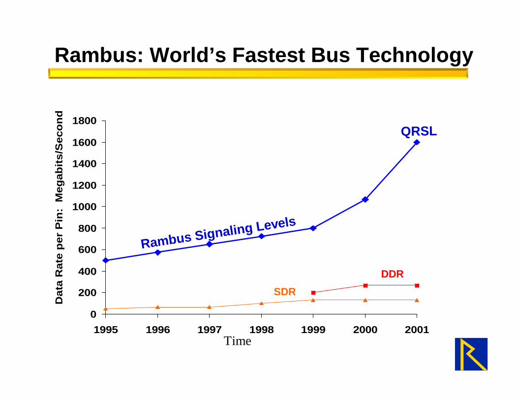
Rambus: World’s Fastest Bus Technology
0
200
400
600
800
1000
1200
1400
1600
1800
1995 1996 1997 1998 1999 2000 2001
Dat
a R
ate
per
Pin
: M
egab
its/
Sec
on
d
Rambus Signaling Levels
QRSL
SDR
DDR
Time

Rambus Market:Rambus Market:Computer, Consumer,Computer, Consumer,CommunicationsCommunications
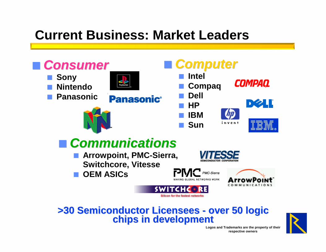
Current Business: Market Leaders
nn ComputerComputern Inteln Compaqn Delln HPn IBMn Sun
nn ConsumerConsumern Sonyn Nintendon Panasonic
>30 Semiconductor Licensees - over 50 logic>30 Semiconductor Licensees - over 50 logicchips in developmentchips in development
nn CommunicationsCommunicationsn Arrowpoint, PMC-Sierra,
Switchcore, Vitessen OEM ASICs
Logos and Trademarks are the property of theirrespective owners

n >45 OEMs shipping PC Systems or Motherboardsn 2nd/3rd Tier companies coming on strongn System Prices Decreasing: $1299 for Dell Optiplex GX200 w/RDRAMn More Rambus-based Platforms to be announced
> 80 RDRAM Based PCs ShippingCompany 820 Based 840 Based
Dimension-XPS B 1GHz Special EditionDimension-XPS B SeriesOptiplex GX200 & GX300 Business PCs
Precision Workstation 220, 420 & 620
Deskpro AP240, AP250Deskpro EN Series
SP 750AP 550
E4400 Series Managed PC E5400 Series Technical Workstation
Aptiva S 1GZPC300PLIntellistation E Pro
Intellistation Z ProIntellistation M Pro
Pavilion 1GVectra VL600
Kayak XU800Kayak XM600ClientPro DX5000
AcerPower 8600
Celsius 440 & 640Primergy B100 & B200Scenic xSi, xB, xL Series
Celsius 650
Logos and Trademarks are the property of theirrespective owners
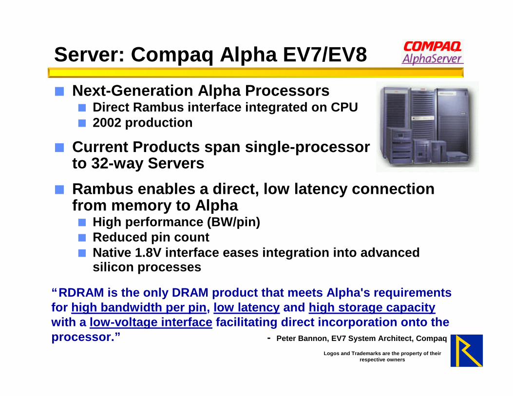
Server: Compaq Alpha EV7/EV8
n Next-Generation Alpha Processorsn Direct Rambus interface integrated on CPUn 2002 production
n Current Products span single-processorto 32-way Servers
n Rambus enables a direct, low latency connectionfrom memory to Alphan High performance (BW/pin)n Reduced pin countn Native 1.8V interface eases integration into advanced
silicon processes
“RDRAM is the only DRAM product that meets Alpha's requirementsfor high bandwidth per pin, low latency and high storage capacitywith a low-voltage interface facilitating direct incorporation onto theprocessor.” - Peter Bannon, EV7 System Architect, Compaq
Logos and Trademarks are the property of theirrespective owners
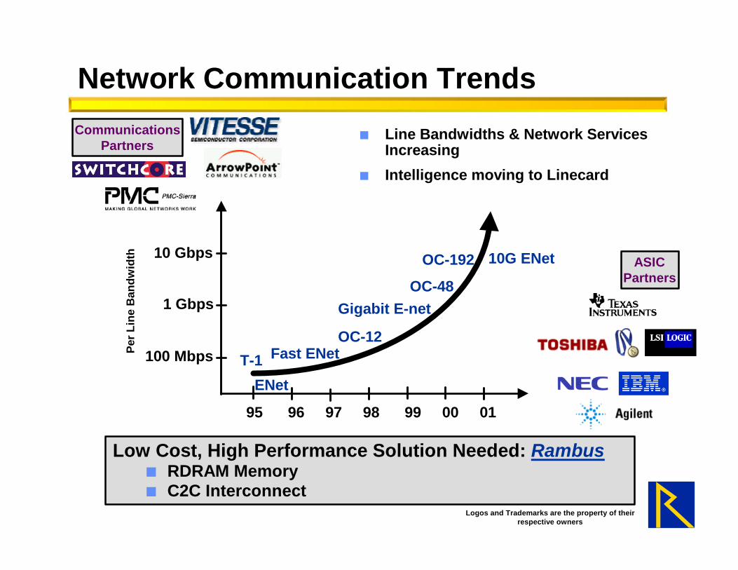
Network Communication Trends
95 96 97 98 99 00 01
10 Gbps
1 Gbps
100 Mbps
ENet
Fast ENet
Gigabit E-net
OC-12
OC-48
OC-192 10G ENet
T-1
Per
Lin
e B
andw
idth
CommunicationsPartners
ASICPartners
Low Cost, High Performance Solution Needed: Rambusn RDRAM Memoryn C2C Interconnect
n Line Bandwidths & Network ServicesIncreasing
n Intelligence moving to Linecard
Logos and Trademarks are the property of theirrespective owners

n 2 ch 800MHz RDRAM = 3.2GB/sn ~140 pins on CPU
Sony PS2: 3.2 GB/s out of 32 MB
Rambus:2 RDRAMs
CPUCPU
n 128b DDR200 bus = 3.2GB/sn ~300 pins on CPU
DDR SDRAM too expensiveDDR SDRAM too expensive
Alternative:8 x16 DDR SDRAMs or 4 x32 SGRAMS
Logos and Trademarks are the property of theirrespective owners

Consumer: Sony PS2 = Simplicityn Integrated Memory
Controller
n Ultra-small formfactor
n Low componentcount
n EE + RDRAM =2.3in2
nn Granularity & LowGranularity & LowPincount =Pincount =Low System CostLow System Cost
• Launched in Japan 3.4.00• 3Mu shipped thru August 2000
GraphicsSynthesizer
EmotionEngine (EE)
2 x 128MbRDRAM
Logos and Trademarks are the property of theirrespective owners

HD-DTVsPanasonicMitsubishi
SanyoSony
Set Top BoxesPanasonicMitsubishi
HitachiPioneer
LCD MonitorsEizo
RDRAM in Consumer Applications

GranularityGranularity
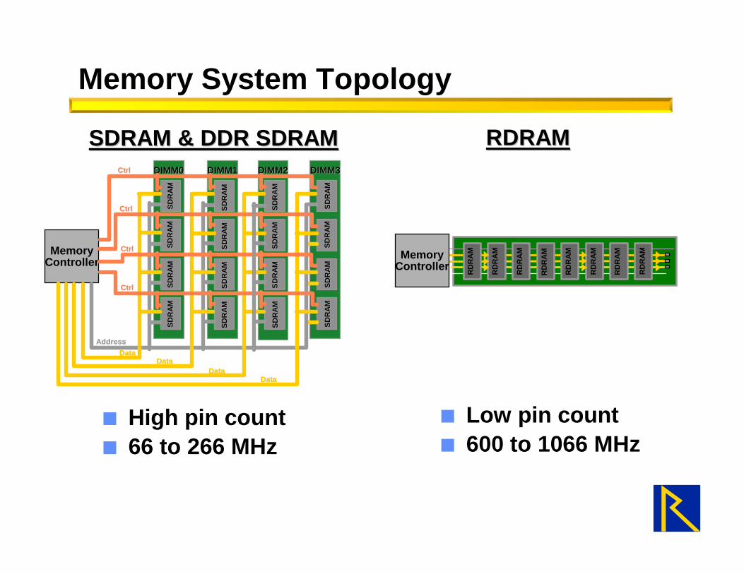
DIMM1DIMM1 DIMM2DIMM2 DIMM3DIMM3
MemoryController
DIMM0DIMM0
DataDataDataData
DataDataDataData
SD
RA
MS
DR
AM
SD
RA
MS
DR
AM
SD
RA
MS
DR
AM
SD
RA
MS
DR
AM
SD
RA
MS
DR
AM
SD
RA
MS
DR
AM
SD
RA
MS
DR
AM
SD
RA
MS
DR
AM
SD
RA
MS
DR
AM
SD
RA
MS
DR
AM
SD
RA
MS
DR
AM
SD
RA
MS
DR
AM
SD
RA
MS
DR
AM
SD
RA
MS
DR
AM
SD
RA
MS
DR
AM
SD
RA
MS
DR
AM
AddressAddress
CtrlCtrl
CtrlCtrl
CtrlCtrl
CtrlCtrl
SDRAM & DDR SDRAMSDRAM & DDR SDRAM RDRAMRDRAM
Memory System Topology
n High pin countn 66 to 266 MHz
n Low pin countn 600 to 1066 MHz
RD
RA
M
RD
RA
M
RD
RA
M
RD
RA
M
RD
RA
M
RD
RA
M
RD
RA
M
RD
RA
MMemoryController

Rambus ChannelRambus Channel
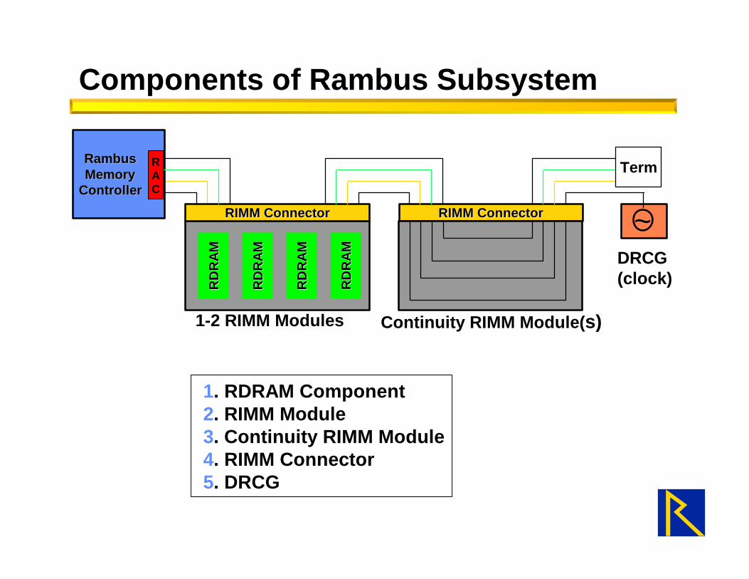
Components of Rambus Subsystem
RD
RA
MR
DR
AM
RD
RA
MR
DR
AM
RD
RA
MR
DR
AM
RD
RA
MR
DR
AM
RambusRambusMemoryMemory
ControllerController
~
1-2 RIMM Modules
DRCG(clock)
RIMM ConnectorRIMM Connector RIMM ConnectorRIMM Connector
Term
Continuity RIMM Module(s)
1. RDRAM Component 2. RIMM Module 3. Continuity RIMM Module 4. RIMM Connector 5. DRCG
RAC

System Memory Topology
MemoryController
Connector
Channel
Termination
n Standard PC Memory Form-Factorn Low-cost, DIMM-like infrastructuren Implementable on standard AT, ATX, micro form-factors
with 4-6 layer motherboard PCBs

Direct Rambus Technology is aSystem Solution
RIMM Connector
DRCG
Direct RDRAM
BusDataBusData BusClkBusClkBusDataBusData
Rambus Memory Controller (RMCD)Rambus Memory Controller (RMCD)
Direct Rambus ASIC Cell (RAC)Direct Rambus ASIC Cell (RAC) ÷4
SynClkSynClk
8 / 9
RD
STA
TU
S
CO
NT
RO
L
AD
DR
ESS
WD
128/144 128/144
8 / 9
ControlControlDirect RAC and RMC
RIMM Module

Thermal InterfaceMaterial (2)
Stamped AluminumHeatspreader (2)
PCB with CSP
RIMM Assembly
EyeletFasteners (4)

RIMM PCB Design
n Critical Component of RIMM Modulen Basis of Rambus Channel transmission linen RDRAM & PCB determines electrical characteristicsn RDRAM electrical parameters carefully controlled
n RIMM Module PCB:n Standard FR-4 Technologyn 6-8 Layer Metal Stack-upn 28Ω Controlled Impedance
CSP Land Pads Bypass Capacitor Pads SPD Pads

PCB Stack-up
5 mil
5 mil (core)
5 mil (core)
5 mil
1.5 oz (finish)
1.5 oz (finish)
1.0 oz
1.0 oz
7 mil
Gnd
Gnd
7 mil
5 mil (core)Gnd
Gnd
50 mils (± 4 mils)
1.0 oz
1.0 oz
1.0 oz
1.0 oz
Vdd
Vref/Vcmos
Signal
Signal
n High-Speed RSL:n Routed in Inner strip-line
layersn 28Ω +/- 10% (unloaded
sections)n Shields signals to EMIn Limits signals to inner layer,
eases process control
n CMOS/Vref layersn Routed in Top µstrip layern 28Ω +/- 15%

RIMM Module Connector
nn HousingHousingn Same body size as DIMMn 168 or 184 pins
nn ContactContactn Electrical specs similar to DIMM connectors:
0.75- 2.0 nH, 0.6-0.85 pFn 1:1 Signal/ground ratio, 1mm pitch
nn Shock and VibrationShock and Vibrationn Latch and hold down mechanisms
nn InsertionsInsertionsn 25 max insertion/withdrawal cycles without plating erosion
Connector SpacingConnector SpacingMin = 0.375” (mfg)Min = 0.375” (mfg)Nom = 0.400” (n.c.)Nom = 0.400” (n.c.)

Impact on Signal Integrity
n Connector is part of the Channel transmission line
n Combination of Connector and PCB Electricalspecifications create a uniform 28 Ohm interface
Motherboard Connector RIMM Connector Motherboard
28 ohm 28 ohm 28 ohm 28 ohm 28 ohm
12
3 4
1 2 3 4

SO-RIMM Modules
n Low Profile Applicationsn Mobile PCsn Handheldsn Networking/Communications
n Termination on motherboard
n 1-8 RDRAMs per SO-RIMM
n 1-3 SO-RIMMs per system
n Same thermal andmechanical envelope as SO-DIMM

Rambus: Broad Range of Configurations
n Short Channeln Solder down RDRAMs to syst PCBn Consumer platformsn Space Constrained applications
(Comms/Networking)
n Long Channeln RIMM modules or SO-RIMM modulen > 1 connector

Agendan Introduction
n Rambus Marketn Rambus Channel
n Configurationn RIMM Modules
n RDRAM CSP Packagingn Requirementsn Various Package solutionsn Ball-out and die shrinkn Thermaln Testing and Surface Mount
n Rambus Technology Roadmap

RDRAM CSP Requirements
n Good electrical performancen High reliabilityn compliance for large dien double sided assemblyn robustness to mechanical shock
n Good heat transfern bare die preferred
n Ease of Assemblyn Competitive cost

Rambus DRAM
n RDRAMn Range of densities, x16 or x18 data bus
n 128/144b RDRAMs available now, 256/288Mb samplingn 800MHz, 700MHz (711MHz), 600MHz speed bins
n CSP (Chip Scale Package)n Electricals enable 800MHz operation
n Short stubs, low inductance, low capacitancen Min ball pitch is 0.8mmx1.0mm, 0.8mmx0.8mmn Signal I/Os placement minimizes PCB layer count
n Designed for low cost in volume
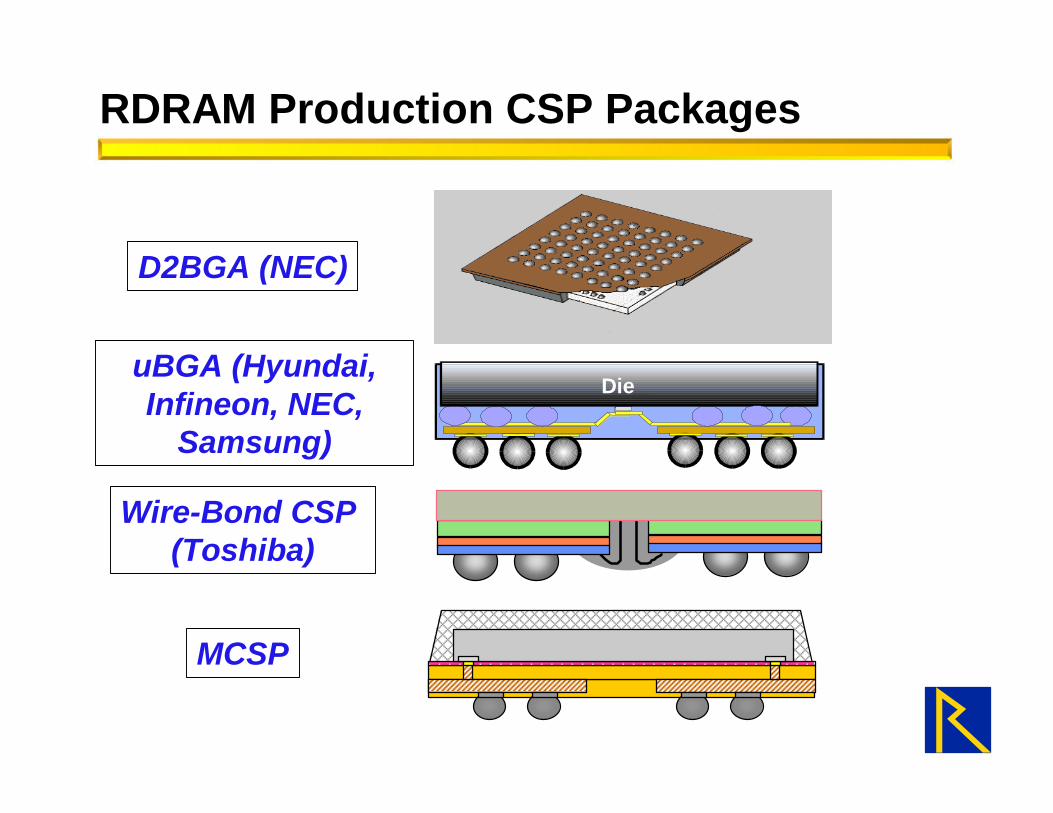
RDRAM Production CSP Packages
uBGA (Hyundai,Infineon, NEC,
Samsung)
MCSP
D2BGA (NEC)
Wire-Bond CSP (Toshiba)
Die
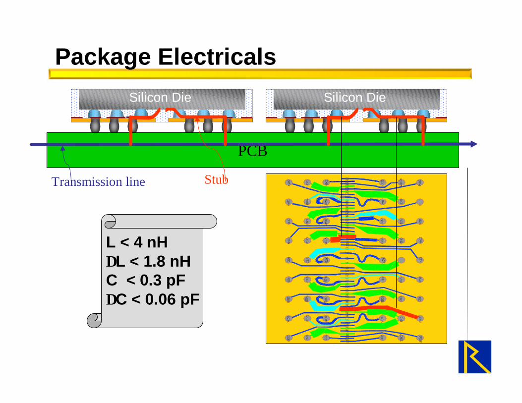
Package Electricals
L < 4 nH∆L < 1.8 nHC < 0.3 pF∆C < 0.06 pF
Silicon Die
PCB
Silicon Die
Transmission line Stub
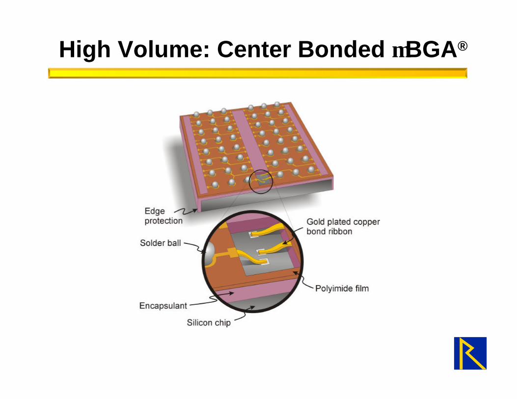
High Volume: Center Bonded µBGA®

High Volume: Wire-Bonded mBGA

Sampling: Rigid Substrate
Bondedwire
Chip
AdhesiveAdhesive
n Good for cost reductionn TAB tape easier to manufacture

Silicon Die
Silicon Die
Silicon Die
Silicon Die
Wirespring
Sampling: FormFactor’s MOST-CSP

N
3
B
10
9
8
A
5
7
6
4
DC E F G H J K L M
2
1
RP S T U
RDRAM Package Footprint
n Option 1: 16*6 electrical ball-out configuration
0.8
mm
0.8 mm

RDRAM Package Footprint
n Option 2: 9*8 electrical ball-out configuration
1 mm
0.8 mm
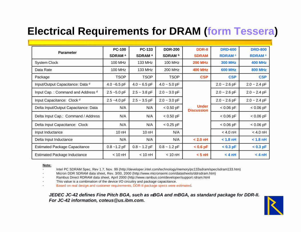
Electrical Requirements for DRAM (form Tessera)
JEDEC JC-42 defines Fine Pitch BGA, such as µBGA and mBGA, as standard package for DDR-II.For JC-42 information, [email protected].
Note:• Intel PC SDRAM Spec, Rev 1.7, Nov. 99 (http://developer.intel.com/technology/memory/pc133sdram/spec/sdram133.htm)• Micron DDR SDRAM data sheet, Rev. 3/00, 2000 (http://www.micronsemi.com/datasheets/ddrsdram.htm)• Rambus Direct RDRAM data sheet, April 2000 (http://www.rambus.com/developer/support rdram.html• This value is a combination of the device I/O circuitry and package capacitance.• Based on real design and customer requirements, DDR-II package specs were estimated.
< 4 nH< 4 nH< 5 nH< 10 nH< 10 nH< 10 nHEstimated Package Inductance
< 0.3 pF< 0.3 pF< 0.6 pF0.8 ~ 1.2 pF0.8 ~ 1.2 pF0.8 ~1.2 pFEstimated Package Capacitance
< 1.8 nH< 1.8 nH< 2.0 nHN/AN/AN/ADelta Input Inductance
< 4.0 nH< 4.0 nHN/A10 nH10 nHInput Inductance
< 0.06 pF< 0.06 pF< 0.25 pFN/AN/ADelta Input Capacitance: Clock
< 0.06 pF< 0.06 pF< 0.50 pFN/AN/ADelta Input Cap.: Command / Address
< 0.06 pF< 0.06 pF< 0.50 pFN/AN/ADelta Input/Output Capacitance: Data
2.0 ~ 2.4 pF2.0 ~ 2.6 pF2.0 ~ 3.0 pF2.5 ~ 3.5 pF2.5 ~4.0 pFInput Capacitance: Clock d
2.0 ~ 2.4 pF2.0 ~ 2.6 pF2.0 ~ 3.0 pF2.5 ~ 3.8 pF2.5 ~5.0 pFInput Cap. : Command and Address d
2.0 ~ 2.4 pF2.0 ~ 2.6 pF
UnderDiscussion
4.0 ~ 5.0 pF4.0 ~ 6.5 pF4.0 ~6.5 pFInput/Output Capacitance: Data d
CSPCSPCSPTSOPTSOPTSOPPackage
800 MHz600 MHz400 MHz200 MHz133 MHz100 MHzData Rate
400 MHz300 MHz200 MHz100 MHz133 MHz100 MHzSystem Clock
DRD-800
RDRAM cDRD-600
RDRAM cDDR-II
SDRAM
DDR-200
SDRAM bPC-133
SDRAM aPC-100
SDRAM aParameter

TSOP Lead Frame and Die Shrink (from Tessera)
Lmax, corner lead =Lmin, center lead =
∆L =
Cmax, corner lead =Cmin, cneter lead =
∆C =
7.6 nH4.8 nH2.8 nH
1.20 pF0.85 pF0.35 pF
8.9 nH4.8 nH4.1 nH
1.44 pF0.85 pF0.59 pF
10.2 nH4.9 nH5.3 nH
1.68 pF0.84 pF0.84 pF
Fixed lead pitch, 0.5 mm, requires excessive fan-out for inner lead design. L and C are toohigh for DDR-II. With die shrink problem becomes worse.
Original Die Shrink Die Excessive Shrink Die
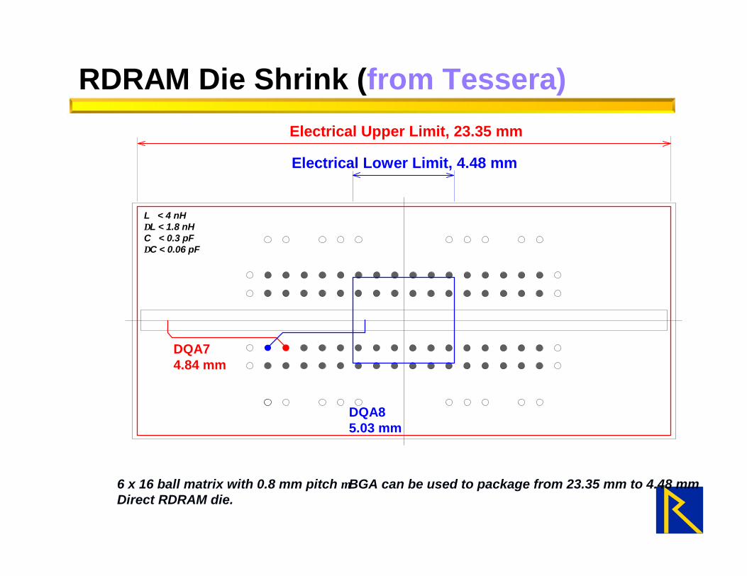
RDRAM Die Shrink (from Tessera)
Electrical Lower Limit, 4.48 mm
Electrical Upper Limit, 23.35 mm
DQA74.84 mm
DQA85.03 mm
L < 4 nH∆L < 1.8 nHC < 0.3 pF ∆C < 0.06 pF
6 x 16 ball matrix with 0.8 mm pitch µBGA can be used to package from 23.35 mm to 4.48 mmDirect RDRAM die.

DRAM Evolution (from Tessera)
Fast Page
EDO
66 MHz SDRAM
100 MHz SDRAM (PC100)
133 MHz SDRAM (PC133)
DDR SDRAM (200 MHz)
DDR II SDRAM (400 MHz)
800 MHz DRDRAM
700 MHz DRDRAM
600 MHz DRDRAM
500 MHz RDRAM
DA
TA R
ATE
TIME
Conventional PKG
CSP or Equivalent
DRAM with higher than 400 MHz data rate requires CSP or electrically CSP equivalentpackage. Early RDRAM used 32-SHP because it has extremely low lead inductance.
32-SHP
TSOP
SOJ
TSOP

ThermalThermal

Peak Module Power
1) PC100 Specification2) Direct RDRAM 72MD-40-800 62/72 Mb Data Sheet DL-0035-00.9
900
mW
900
mW
900
mW
900
mW
900
mW
900
mW
900
mW
900
mW
900
mW
250
mW
250
mW
625
mW
1165
mW
625
mW
625
mW
250
mW
250
mW
DIMM Module Power1
8.1 W
RIMM Module Power2
4.0 W
800 MB/s
1600 MB/s
Twice the Bandwidth at Half the Power!
4 Power Saving ModesPower Legend:1165mW = ACTR + I/O625mW = ATTN + Core250mW = STBY
Assuming 4Assuming 4outstandingoutstanding
memorymemoryrequestsrequests
RDRAM: Lowest Average Power

TestingTesting

RDRAM Package Testing
nSockets are available thatnMinimize parasitic inductancenMake good contactnAvoid marking solder ballnSupport many insertionsnAdapt to multiple CSP sizes
nAt-Speed testingnMinimum InductancenShort test times, very high number of insertions
nBurn-in testingnReliability required over thermal cycles

Solder Ball Interface: Many options
n Pinch or Tweezer contactsn Grip top or side of ball to minimize damage at solder
pointn Break oxide on ball, make good contactn Longer contact length to reach top of ball
n Elastomer Contactsn Very short contact, low inductancen Bottom of solder ball contacts elastomern Long life, but elastomer may become contaminated
over time resulting in slow test degradation
nSpring or Pogo-Pin Contactsn Very long life. Failing pins are apparentn Contact bottom of solder balln Inductance depends on length of contact
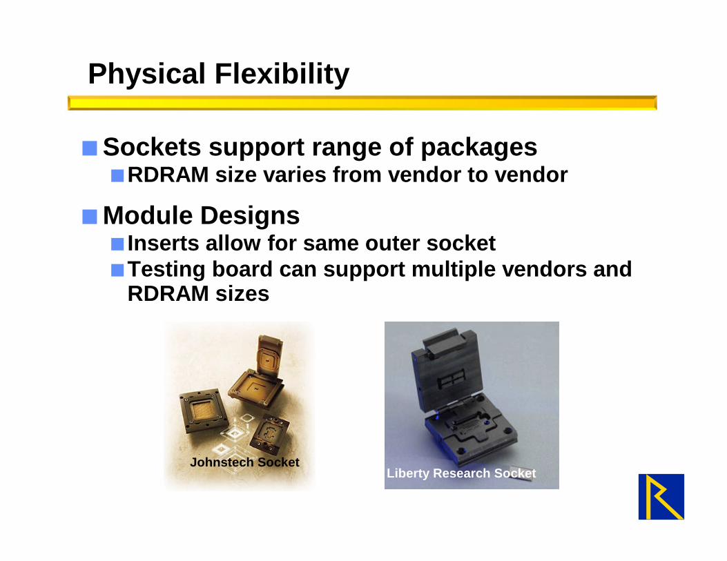
Physical Flexibility
nSockets support range of packagesnRDRAM size varies from vendor to vendor
nModule Designsn Inserts allow for same outer socketnTesting board can support multiple vendors and
RDRAM sizes
Johnstech SocketLiberty Research Socket

Available Sockets
nClamshell and Open top
nSingle and Multi-site
Liberty Research Multi-Site Burn-in Socket
Liberty Research Burn-in Socket 3M MicroTouchTM Socket
Surface MountSurface Mount

RIMM Module Assembly
n CSP Surface Mount Technology Uses Standard SMT process.
n Precision Pick-and-PlaceHandler
n CSP loading capabilityn 1mil precision placement
n Convection Reflow Ovenn Flow Uniformity
Critical to yield
Photo courtesy of Tessera.
Photo courtesy of Fuji

Assembly Yield
n Assembly yields are typically >>99%
n Temperature reflow profile is the criticalparameter
n Flux application and solder stencil are key toprevent bridging and shorts

ReliabilityReliability

CSP Reliability
n To evaluate the reliability of the CSP package asmounted on RIMM module with heat spreader
n Consortium of many assemblers, suppliers andRambus
n 128Mb reliability used uBGA (finished ‘99)256Mb reliability uses various CSP’s (on going)
n Daisy chain device and daisy chain modules areused
n Reliability test criteria established jointly by Inteland Rambus

Test Condition Number of dies
1 Temperature Cycle 1 Per EIA 364, TP32B: 1000 Cycles (0 C/+100C), 15 minutedwell at each temp including ramp time, temp recovery time <5minutes
48
2 Temperature Cycle 2 Per EIA 364, TP32B: 1000 cycles (-40 C/+85 C), 15 minutedwell at each temp including ramp time, temp recovery timeshould be < 5minutes
48
3 Cyclic Humidity Per EIA 364, TP31 A, Condition III (Omit steps 7A and 7B):25C to 65C @ 90-95% relative humidity(non condensing); 240hours (10 cycles)
48
4 High Temperature Storage Per EIA 364, TP17A, Method A: 1000 hours at 100C 48
5 Mechanical Shock Per EIA 364, TP27B, Condition G: 100 g’s, saw tooth wave, 6ms, three shocks/direction/axis (18 shocks)
48
6 Random Vibration Per EIA 364, TP48D, Condition 5B: 50-2000 Hz, 7.3 g RMS,45 minutes/axis, test in each of 3 axes
48
7 Twist Test Clamp on one end of module and twist the other end withtorque of 1.236 N-m or 10 degrees (whichever comes first),clockwise and counter clockwise. Twist and hold for 5 minutes,repeat in other direction. Repeat cycle 5 times each direction
48
8 Drop Test Drop module on all six surfaces and all four corners from aheight of 30-34 inches onto a non-cushioning vinyl-tile surface(10 drops total per module)
48
9 3 Point bending With module supported at both ends, a cyclic load of 14.5 lbsor 0.25 inch deflection (rate of 1 inch per minute displacement)must be sustained for duration of 2 minutes. Cycle period is 3minutes. Repeat cycle 5 times. Repeat test with modulerotated 180 degrees. Point load actuator should be 0.25 inchdiameter.
48
10 Compression / Pinch Apply a constant 23 psi (1 inch/minute displacement) load byforce displacement (Instron like machine) for duration of 20seconds, period of 1 minute. Repeat for 10 cycles
48
Reliability Conditions for Assembled Module
Wafer LevelWafer Level

CSP trend: Wafer Level for RDRAM
wsCSP
Ultra CSP
Super CSP
MOST CSP
WAVE
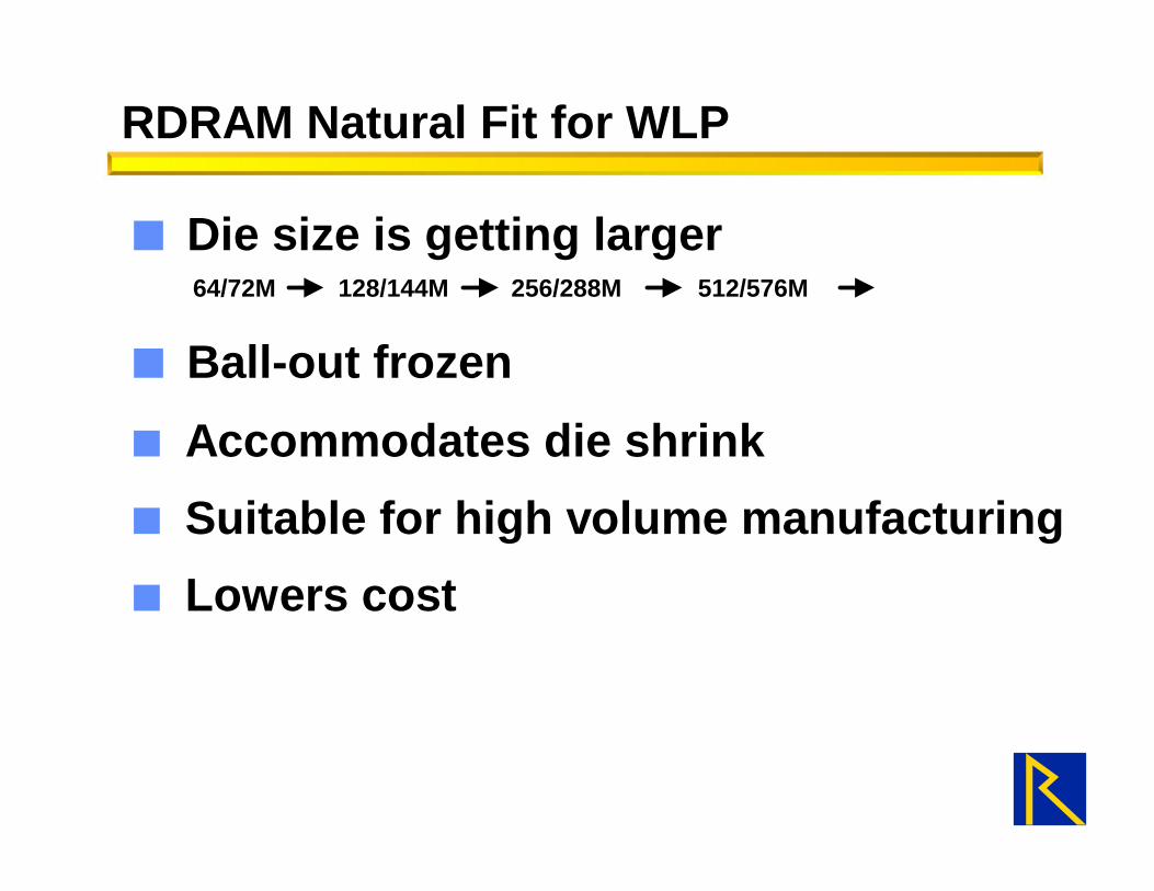
RDRAM Natural Fit for WLP
n Die size is getting larger 64/72M 128/144M 256/288M 512/576M
n Ball-out frozen
n Accommodates die shrink
n Suitable for high volume manufacturing
n Lowers cost
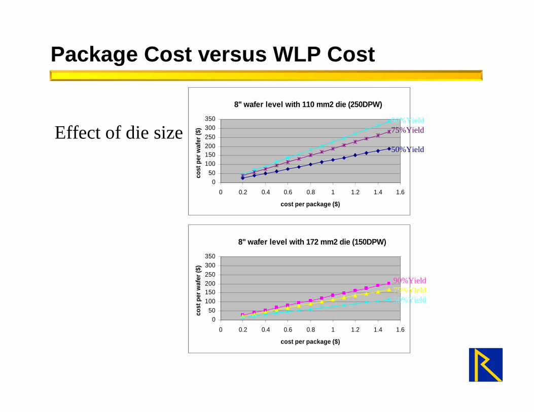
8" wafer level with 110 mm2 die (250DPW)
050
100150200250300350
0 0.2 0.4 0.6 0.8 1 1.2 1.4 1.6
cost per package ($)co
st p
er w
afer
($)
90%Yield75%Yield
50%Yield
8" wafer level with 172 mm2 die (150DPW)
050
100150200250300350
0 0.2 0.4 0.6 0.8 1 1.2 1.4 1.6
cost per package ($)
cost
per
waf
er ($
)
90%Yield75%Yield50%Yield
Effect of die size
Package Cost versus WLP Cost

Desired WLP cost for 200 DPW
cost of 8" wafer at 90% yield
0
50
100
150
200
0 0.2 0.4 0.6 0.8 1 1.2
cost per package ($)
cost
per
waf
er ($
) 200DPW
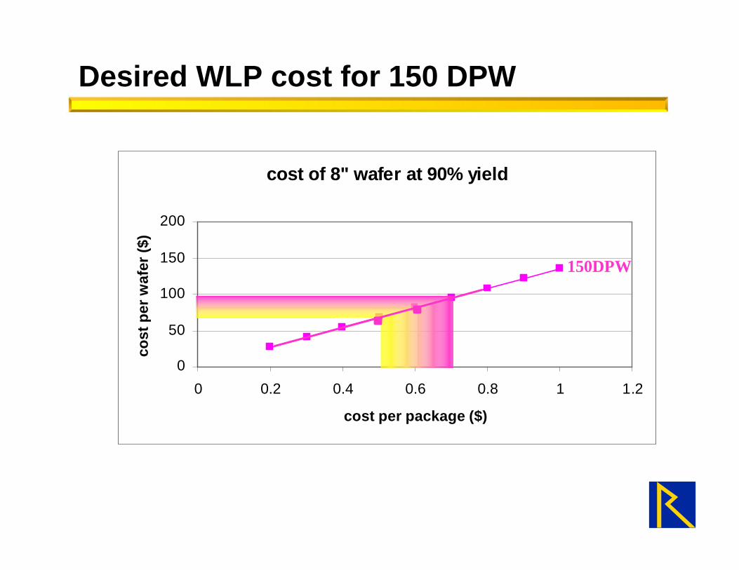
Desired WLP cost for 150 DPW
cost of 8" wafer at 90% yield
0
50
100
150
200
0 0.2 0.4 0.6 0.8 1 1.2
cost per package ($)
cost
per
waf
er ($
)
150DPW

Source: Dataquest 11/99
1998 1999 2000 2001 2002 CAGR 1998-2002
Chipscale 356 1020 2300 4500 6500 78.80%Plastic BGA 2664 3400 4321 5900 7600 23.30%Ceramic BGA 194 278 378 444 504 21.00%Bare chip 3042 3700 4180 4400 5000 10.40%SO 34516 35989 38300 42000 46000 5.90%QFP 14187 13429 12989 12119 11654 -3.90%Ceramic PGA 134 109 101 94 89 -7.90%Ceramic DIP 137 120 100 95 86 -8.90%Plastic PGA 98 81 70 62 50 -12.60%Plastic chip carrier 641 566 489 320 280 -15.30%Ceramic chip carrier 18 12 9 7 4 -26%Plastic DIP 1959 1222 900 544 418 -26.60%Other 1983 2560 2900 3090 3300 10.70%
Total IC units 599292 62486 67037 73575 81485 6.30%
Worldwide IC Package Production, Millions of Units
CSP Market: Growing Fast
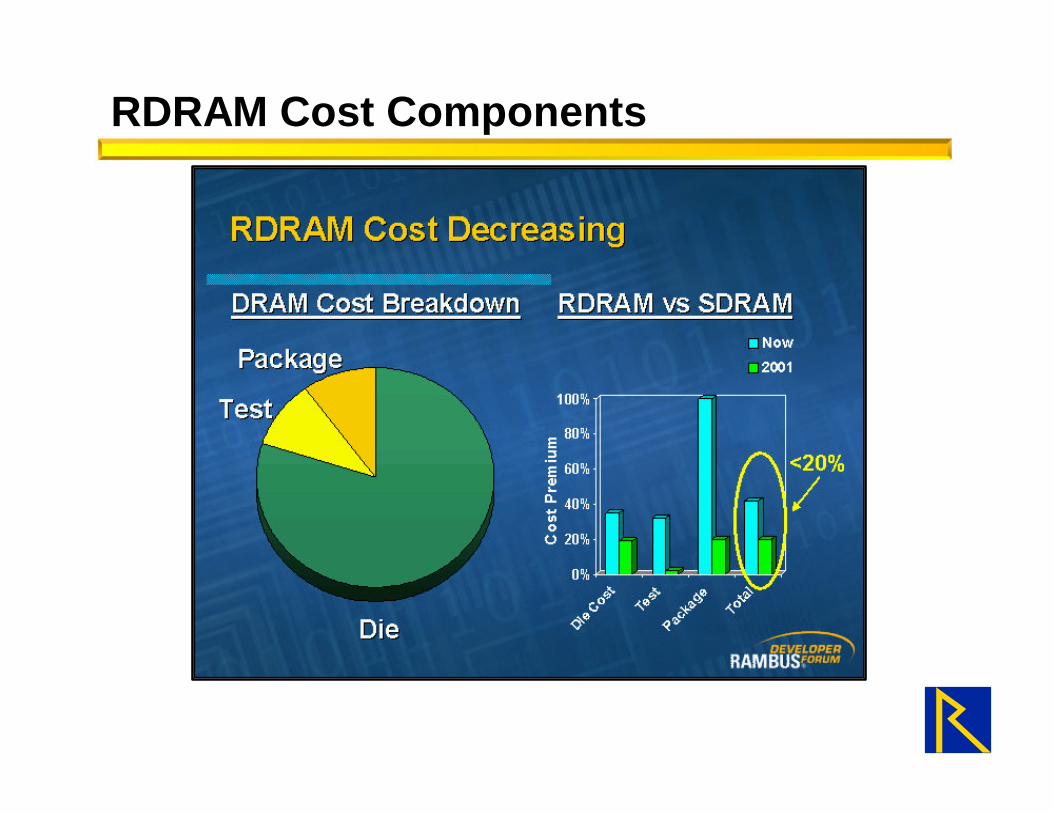
RDRAM Cost Components

RDRAM Cost Premium: 5% in 2002

Agendan Introduction
n Rambus Marketn Rambus Channel
n Configurationn RIMM Modules
n RDRAM CSP Packagingn Requirementsn Various Package solutionsn Ball-out and die shrinkn Thermaln Testing and Surface Mount
n Rambus Technology Roadmap

Rambus Signaling Solutions
SerDes
QRSL
RSL
Links
Buses
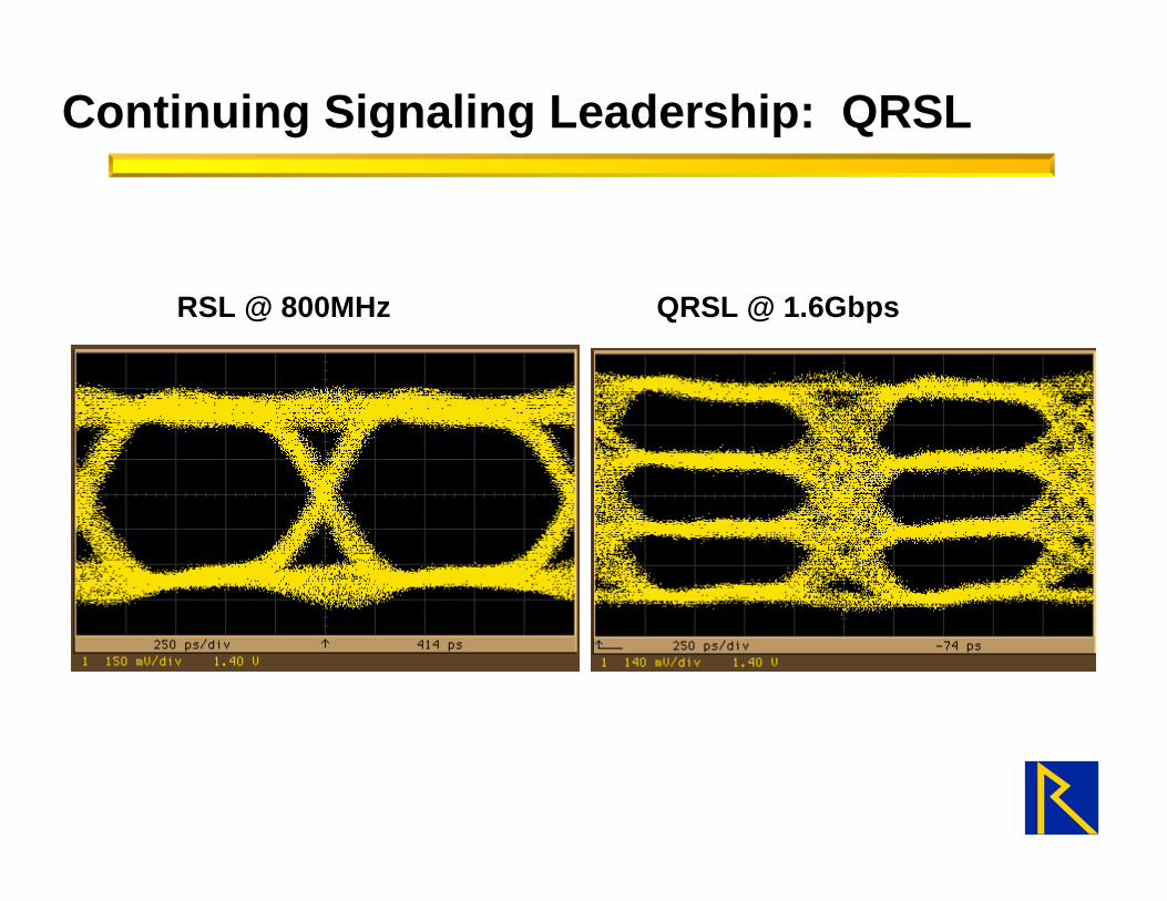
Continuing Signaling Leadership: QRSL
RSL @ 800MHz QRSL @ 1.6Gbps

QRSL: 12 times Bandwidth of PC133
Bus Width
Bits / Clock
Clock (MHz)
64
128
1
2
4
200 300 400 500
1.0 GB/s
Bits / Clock
Clock (MHz)
64
128
2
4
200 300 400 500
2.1 GB/s
Bus Width
Bits / Clock
Clock (MHz)
64
128
2
4
400 500
6.4 GB/s
Bus Width
Bits / Clock
Clock (MHz)
64
128
4
400 500
12.8 GB/s
Bus Width
PC133SDRAM
DDR266SDRAM
800MHzRDRAM
QRSL