p spice for circuit theory and electronic devices
TRANSCRIPT

MOBK059-FM MOBKXXX-Sample.cls March 9, 2007 10:43
PSpice for Circuit Theory andElectronic Devices

MOBK059-FM MOBKXXX-Sample.cls March 12, 2007 13:41
Copyright © 2007 by Morgan & Claypool
All rights reserved. No part of this publication may be reproduced, stored in a retrieval system, or transmitted in
any form or by any means—electronic, mechanical, photocopy, recording, or any other except for brief quotations
in printed reviews, without the prior permission of the publisher.
PSpice for Circuit Theory and Electronic Devices
Paul Tobin
www.morganclaypool.com
ISBN: 1598291564 paperback
ISBN: 9781598291568 paperback
ISBN: 1598291572 ebook
ISBN: 9781598291575 ebook
DOI: 10.2200/S00068ED1V01Y200611DCS007
A Publication in the Morgan & Claypool Publishers series
SYNTHESIS LECTURES ON DIGITAL CIRCUITS AND SYSTEMS #7
Lecture #7
Series Editor: Mitchell A. Thornton, Southern Methodist University
Library of Congress Cataloging-in-Publication Data
Series ISSN: 1932-3166 print
Series ISSN: 1932-3174 electronic
First Edition
10 9 8 7 6 5 4 3 2 1

MOBK059-FM MOBKXXX-Sample.cls March 12, 2007 13:41
PSpice for Circuit Theory andElectronic Devices
Paul TobinSchool of Electronic and Communications Engineering
Dublin Institute of Technology
Ireland
SYNTHESIS LECTURES ON DIGITAL CIRCUITS AND SYSTEMS #7
M&C
M o r g a n & C l a y p o o l P u b l i s h e r s
MOBK059-FM MOBKXXX-Sample.cls March 9, 2007 10:43
iv
ABSTRACTPSpice for Circuit Theory and Electronic Devices is one of a series of five PSpice books and
introduces the latest Cadence Orcad PSpice version 10.5 by simulating a range of DC and AC
exercises. It is aimed primarily at those wishing to get up to speed with this version but will be of
use to high school students, undergraduate students, and of course, lecturers. Circuit theorems
are applied to a range of circuits and the calculations by hand after analysis are then compared
to the simulated results. The Laplace transform and the s-plane are used to analyze CR and
LR circuits where transient signals are involved. Here, the Probe output graphs demonstrate
what a great learning tool PSpice is by providing the reader with a visual verification of
any theoretical calculations. Series and parallel-tuned resonant circuits are investigated where
the difficult concepts of dynamic impedance and selectivity are best understood by sweeping
different circuit parameters through a range of values.
Obtaining semiconductor device characteristics as a laboratory exercise has fallen out
of favour of late, but nevertheless, is still a useful exercise for understanding or modelling
semiconductor devices. Inverting and non-inverting operational amplifiers characteristics such
as gain-bandwidth are investigated and we will see the dependency of bandwidth on the gain
using the performance analysis facility. Power amplifiers are examined where PSpice/Probe
demonstrates very nicely the problems of cross-over distortion and other problems associated
with power transistors. We examine power supplies and the problems of regulation, ground
bounce, and power factor correction. Lastly, we look at MOSFET device characteristics and
show how these devices are used to form basic CMOS logic gates such as NAND and NOR
gates.
KEYWORDSCadence Orcad PSpice V10.5, Ohm’s law, Kirchhoff’s laws, Thevenin and Norton theorems,
Mesh and nodal analysis, Laplace, transients, transfer functions, resonance, transformers, power
supplies, ground bounce, operational amplifiers, power amplifiers.

MOBK059-FM MOBKXXX-Sample.cls March 9, 2007 10:43
I would like to dedicate this book to my wife and friend,Marie and sons Lee, Roy, Scott and Keith and my
parents (Eddie and Roseanne), sisters, Sylvia,Madeleine, Jean, and brother, Ted.

MOBK059-FM MOBKXXX-Sample.cls March 9, 2007 10:43

MOBK059-FM MOBKXXX-Sample.cls March 9, 2007 10:43
vii
Contents
Preface . . . . . . . . . . . . . . . . . . . . . . . . . . . . . . . . . . . . . . . . . . . . . . . . . . . . . . . . . . . . . . . . . . . . . . xiii
1. Introduction to PSpice and Ohm’s Law . . . . . . . . . . . . . . . . . . . . . . . . . . . . . . . . . . . . . . . . . 1
1.1 Laying out A Schematic . . . . . . . . . . . . . . . . . . . . . . . . . . . . . . . . . . . . . . . . . . . . . . . . . . 1
1.2 Libraries . . . . . . . . . . . . . . . . . . . . . . . . . . . . . . . . . . . . . . . . . . . . . . . . . . . . . . . . . . . . . . . . .2
1.2.1 Moving Components Around . . . . . . . . . . . . . . . . . . . . . . . . . . . . . . . . . . . . . . 4
1.2.2 Display Properties . . . . . . . . . . . . . . . . . . . . . . . . . . . . . . . . . . . . . . . . . . . . . . . . 5
1.3 The DC Circuit . . . . . . . . . . . . . . . . . . . . . . . . . . . . . . . . . . . . . . . . . . . . . . . . . . . . . . . . . 6
1.3.1 New Simulation . . . . . . . . . . . . . . . . . . . . . . . . . . . . . . . . . . . . . . . . . . . . . . . . . . 7
1.3.2 Main Operational Icons . . . . . . . . . . . . . . . . . . . . . . . . . . . . . . . . . . . . . . . . . . . 8
1.3.3 Simulation Settings . . . . . . . . . . . . . . . . . . . . . . . . . . . . . . . . . . . . . . . . . . . . . . . 9
1.4 Potential Divider . . . . . . . . . . . . . . . . . . . . . . . . . . . . . . . . . . . . . . . . . . . . . . . . . . . . . . . . 9
1.4.1 Current Divider . . . . . . . . . . . . . . . . . . . . . . . . . . . . . . . . . . . . . . . . . . . . . . . . . 11
1.5 Exercises . . . . . . . . . . . . . . . . . . . . . . . . . . . . . . . . . . . . . . . . . . . . . . . . . . . . . . . . . . . . . . . 12
2. The DC Circuit and Kirchhoff’s Laws . . . . . . . . . . . . . . . . . . . . . . . . . . . . . . . . . . . . . . . . . 13
2.1 Maximum Power Transfer . . . . . . . . . . . . . . . . . . . . . . . . . . . . . . . . . . . . . . . . . . . . . . . 13
2.1.1 Param Part . . . . . . . . . . . . . . . . . . . . . . . . . . . . . . . . . . . . . . . . . . . . . . . . . . . . . . 13
2.1.2 Simulation Settings . . . . . . . . . . . . . . . . . . . . . . . . . . . . . . . . . . . . . . . . . . . . . . 13
2.1.3 Trace Expression Box . . . . . . . . . . . . . . . . . . . . . . . . . . . . . . . . . . . . . . . . . . . . 15
2.2 Changing the X-Axis Variable . . . . . . . . . . . . . . . . . . . . . . . . . . . . . . . . . . . . . . . . . . . 16
2.2.1 The Log Command . . . . . . . . . . . . . . . . . . . . . . . . . . . . . . . . . . . . . . . . . . . . . . 17
2.3 Mesh Analysis . . . . . . . . . . . . . . . . . . . . . . . . . . . . . . . . . . . . . . . . . . . . . . . . . . . . . . . . . . 17
2.4 Nodal Analysis . . . . . . . . . . . . . . . . . . . . . . . . . . . . . . . . . . . . . . . . . . . . . . . . . . . . . . . . . . 20
2.5 Exercises . . . . . . . . . . . . . . . . . . . . . . . . . . . . . . . . . . . . . . . . . . . . . . . . . . . . . . . . . . . . . . . 22
3. Transient Circuits and Laplace Transforms . . . . . . . . . . . . . . . . . . . . . . . . . . . . . . . . . . . . 23
3.1 Transient Analysis . . . . . . . . . . . . . . . . . . . . . . . . . . . . . . . . . . . . . . . . . . . . . . . . . . . . . . 23
3.2 Laplace Transform and Capacitance . . . . . . . . . . . . . . . . . . . . . . . . . . . . . . . . . . . . . . 23
3.3 Inductance . . . . . . . . . . . . . . . . . . . . . . . . . . . . . . . . . . . . . . . . . . . . . . . . . . . . . . . . . . . . . 24
3.4 First-Order CR and LR Circuits . . . . . . . . . . . . . . . . . . . . . . . . . . . . . . . . . . . . . . . . . .24
3.4.1 Solution . . . . . . . . . . . . . . . . . . . . . . . . . . . . . . . . . . . . . . . . . . . . . . . . . . . . . . . . 25
3.4.2 Partial Fraction Expansion . . . . . . . . . . . . . . . . . . . . . . . . . . . . . . . . . . . . . . . . 26
MOBK059-FM MOBKXXX-Sample.cls March 9, 2007 10:43
viii PSPICE FOR CIRCUIT THEORY AND ELECTRONIC DEVICES
3.4.3 Initial Conditions . . . . . . . . . . . . . . . . . . . . . . . . . . . . . . . . . . . . . . . . . . . . . . . . 27
3.5 Example 2 . . . . . . . . . . . . . . . . . . . . . . . . . . . . . . . . . . . . . . . . . . . . . . . . . . . . . . . . . . . . . . 28
3.5.1 Solution . . . . . . . . . . . . . . . . . . . . . . . . . . . . . . . . . . . . . . . . . . . . . . . . . . . . . . . . 28
3.6 Example 3 . . . . . . . . . . . . . . . . . . . . . . . . . . . . . . . . . . . . . . . . . . . . . . . . . . . . . . . . . . . . . . 29
3.6.1 Solution . . . . . . . . . . . . . . . . . . . . . . . . . . . . . . . . . . . . . . . . . . . . . . . . . . . . . . . . 30
3.7 Example 4 . . . . . . . . . . . . . . . . . . . . . . . . . . . . . . . . . . . . . . . . . . . . . . . . . . . . . . . . . . . . . . 32
3.7.1 Solution . . . . . . . . . . . . . . . . . . . . . . . . . . . . . . . . . . . . . . . . . . . . . . . . . . . . . . . . 33
3.8 Exercise . . . . . . . . . . . . . . . . . . . . . . . . . . . . . . . . . . . . . . . . . . . . . . . . . . . . . . . . . . . . . . . . 34
4. Transfer Functions and System Parameters . . . . . . . . . . . . . . . . . . . . . . . . . . . . . . . . . . . . 35
4.1 Transfer Functions . . . . . . . . . . . . . . . . . . . . . . . . . . . . . . . . . . . . . . . . . . . . . . . . . . . . . . 35
4.2 Butterworth Transfer Functions and the Laplace Part . . . . . . . . . . . . . . . . . . . . . . . 35
4.2.1 Piece-wise Linear Part (VPWL) . . . . . . . . . . . . . . . . . . . . . . . . . . . . . . . . . . 37
4.3 Probe Grid and Cursors Icons . . . . . . . . . . . . . . . . . . . . . . . . . . . . . . . . . . . . . . . . . . . . 37
4.4 Elaplace Part and the Step Response . . . . . . . . . . . . . . . . . . . . . . . . . . . . . . . . . . . . . . 38
4.5 Chebychev Transfer Functions Impulse Response . . . . . . . . . . . . . . . . . . . . . . . . . . 40
4.5.1 Unsynchronizing Probe Plots . . . . . . . . . . . . . . . . . . . . . . . . . . . . . . . . . . . . . 42
4.6 First-Order Low-Pass Filter Step and Impulse Responses . . . . . . . . . . . . . . . . . . . 42
4.7 Obtaining the Frequency Response from the Impulse Response . . . . . . . . . . . . . . 44
4.8 The Low-Pass C R Filter Step Response . . . . . . . . . . . . . . . . . . . . . . . . . . . . . . . . . . . 45
4.9 Rise Time . . . . . . . . . . . . . . . . . . . . . . . . . . . . . . . . . . . . . . . . . . . . . . . . . . . . . . . . . . . . . . 46
4.10 Step Response of a Series-Tuned LCR Circuit . . . . . . . . . . . . . . . . . . . . . . . . . . . . . 48
4.10.1 Overshoot . . . . . . . . . . . . . . . . . . . . . . . . . . . . . . . . . . . . . . . . . . . . . . . . . . . . . . .48
4.11 Exercises . . . . . . . . . . . . . . . . . . . . . . . . . . . . . . . . . . . . . . . . . . . . . . . . . . . . . . . . . . . . . . . 48
5. AC Circuits and Circuit Theorems . . . . . . . . . . . . . . . . . . . . . . . . . . . . . . . . . . . . . . . . . . . . 53
5.1 AC Circuit Theory . . . . . . . . . . . . . . . . . . . . . . . . . . . . . . . . . . . . . . . . . . . . . . . . . . . . . 53
5.2 Capacitors . . . . . . . . . . . . . . . . . . . . . . . . . . . . . . . . . . . . . . . . . . . . . . . . . . . . . . . . . . . . . 53
5.2.1 Capacitive Reactance Plot . . . . . . . . . . . . . . . . . . . . . . . . . . . . . . . . . . . . . . . . 54
5.2.2 Capacitor Current and Voltage Waveforms . . . . . . . . . . . . . . . . . . . . . . . . .55
5.3 Inductors . . . . . . . . . . . . . . . . . . . . . . . . . . . . . . . . . . . . . . . . . . . . . . . . . . . . . . . . . . . . . . . 56
5.3.1 Inductor Signal Phase Measurement . . . . . . . . . . . . . . . . . . . . . . . . . . . . . . 58
5.4 AC Circuit Theorems . . . . . . . . . . . . . . . . . . . . . . . . . . . . . . . . . . . . . . . . . . . . . . . . . . . 58
5.4.1 Thevenin’s Theorem . . . . . . . . . . . . . . . . . . . . . . . . . . . . . . . . . . . . . . . . . . . . .59
5.4.2 Thevenin Impedance . . . . . . . . . . . . . . . . . . . . . . . . . . . . . . . . . . . . . . . . . . . . . 60
5.4.3 Thevenin Voltage . . . . . . . . . . . . . . . . . . . . . . . . . . . . . . . . . . . . . . . . . . . . . . . . 61
5.5 Norton Equivalent Circuit . . . . . . . . . . . . . . . . . . . . . . . . . . . . . . . . . . . . . . . . . . . . . . . 61
5.5.1 The Output File . . . . . . . . . . . . . . . . . . . . . . . . . . . . . . . . . . . . . . . . . . . . . . . . . 62

MOBK059-FM MOBKXXX-Sample.cls March 9, 2007 10:43
CONTENTS ix
5.6 AC Mesh and Nodal Analysis . . . . . . . . . . . . . . . . . . . . . . . . . . . . . . . . . . . . . . . . . . . . 62
5.7 Exercises . . . . . . . . . . . . . . . . . . . . . . . . . . . . . . . . . . . . . . . . . . . . . . . . . . . . . . . . . . . . . . . 62
6. Series and Parallel-tuned Resonance. . . . . . . . . . . . . . . . . . . . . . . . . . . . . . . . . . . . . . . . . . .65
6.1 Resonance . . . . . . . . . . . . . . . . . . . . . . . . . . . . . . . . . . . . . . . . . . . . . . . . . . . . . . . . . . . . . 65
6.2 Series-Tuned Circuit . . . . . . . . . . . . . . . . . . . . . . . . . . . . . . . . . . . . . . . . . . . . . . . . . . . .65
6.2.1 Current Response . . . . . . . . . . . . . . . . . . . . . . . . . . . . . . . . . . . . . . . . . . . . . . . . 66
6.3 Example . . . . . . . . . . . . . . . . . . . . . . . . . . . . . . . . . . . . . . . . . . . . . . . . . . . . . . . . . . . . . . . 67
6.3.1 Solution . . . . . . . . . . . . . . . . . . . . . . . . . . . . . . . . . . . . . . . . . . . . . . . . . . . . . . . . 67
6.4 Q-Factor . . . . . . . . . . . . . . . . . . . . . . . . . . . . . . . . . . . . . . . . . . . . . . . . . . . . . . . . . . . . . . . 67
6.4.1 The −3 dB Bandwidth . . . . . . . . . . . . . . . . . . . . . . . . . . . . . . . . . . . . . . . . . . . 67
6.5 Voltages Across L and C at Resonance . . . . . . . . . . . . . . . . . . . . . . . . . . . . . . . . . . . . 68
6.6 Universal Response Curve . . . . . . . . . . . . . . . . . . . . . . . . . . . . . . . . . . . . . . . . . . . . . . . . 70
6.7 Selectivity of a Series-Tuned Resonant Circuit . . . . . . . . . . . . . . . . . . . . . . . . . . . . .70
6.7.1 L/C Ratio and Selectivity . . . . . . . . . . . . . . . . . . . . . . . . . . . . . . . . . . . . . . . . 72
6.8 Series-Tuned LC R Phase Response. . . . . . . . . . . . . . . . . . . . . . . . . . . . . . . . . . . . . . .72
6.9 Impedance of a Series-Tuned Circuit . . . . . . . . . . . . . . . . . . . . . . . . . . . . . . . . . . . . . .73
6.10 Fourier Series . . . . . . . . . . . . . . . . . . . . . . . . . . . . . . . . . . . . . . . . . . . . . . . . . . . . . . . . . . . 74
6.10.1 Series-Tuned Circuit as a Low-Pass Filter . . . . . . . . . . . . . . . . . . . . . . . . . 74
6.10.2 The Output File . . . . . . . . . . . . . . . . . . . . . . . . . . . . . . . . . . . . . . . . . . . . . . . . . 75
6.11 Skip Initial Conditions . . . . . . . . . . . . . . . . . . . . . . . . . . . . . . . . . . . . . . . . . . . . . . . . . . 76
6.12 Parallel-Tuned LC R Circuit . . . . . . . . . . . . . . . . . . . . . . . . . . . . . . . . . . . . . . . . . . . . . 77
6.12.1 Universal Response Curve . . . . . . . . . . . . . . . . . . . . . . . . . . . . . . . . . . . . . . . . 80
6.12.2 Relationship Between the Resonant Frequency and Bandwidth . . . . . . . 81
6.12.3 Loaded Q-factor . . . . . . . . . . . . . . . . . . . . . . . . . . . . . . . . . . . . . . . . . . . . . . . . .81
6.13 Example. . . . . . . . . . . . . . . . . . . . . . . . . . . . . . . . . . . . . . . . . . . . . . . . . . . . . . . . . . . . . . . .82
6.13.1 Solution . . . . . . . . . . . . . . . . . . . . . . . . . . . . . . . . . . . . . . . . . . . . . . . . . . . . . . . . 82
6.14 Problem . . . . . . . . . . . . . . . . . . . . . . . . . . . . . . . . . . . . . . . . . . . . . . . . . . . . . . . . . . . . . . . . 82
6.15 Frequency Response of a Parallel-Tuned Circuit . . . . . . . . . . . . . . . . . . . . . . . . . . . 83
6.16 Dynamic Impedance . . . . . . . . . . . . . . . . . . . . . . . . . . . . . . . . . . . . . . . . . . . . . . . . . . . . .84
6.16.1 Loaded and Unloaded Q-factor . . . . . . . . . . . . . . . . . . . . . . . . . . . . . . . . . . . 84
6.17 Transformers . . . . . . . . . . . . . . . . . . . . . . . . . . . . . . . . . . . . . . . . . . . . . . . . . . . . . . . . . . . 88
6.17.1 Transformer Parameters . . . . . . . . . . . . . . . . . . . . . . . . . . . . . . . . . . . . . . . . . 89
6.17.2 Matching Transformer . . . . . . . . . . . . . . . . . . . . . . . . . . . . . . . . . . . . . . . . . . . 89
6.18 Power Supplies: Rectification and Regulation . . . . . . . . . . . . . . . . . . . . . . . . . . . . . . 90
6.18.1 Power Supply Waveforms . . . . . . . . . . . . . . . . . . . . . . . . . . . . . . . . . . . . . . . . 91
6.18.2 Power Supply Voltage Regulation . . . . . . . . . . . . . . . . . . . . . . . . . . . . . . . . . 91

MOBK059-FM MOBKXXX-Sample.cls March 9, 2007 10:43
x PSPICE FOR CIRCUIT THEORY AND ELECTRONIC DEVICES
6.19 Ground Bounce . . . . . . . . . . . . . . . . . . . . . . . . . . . . . . . . . . . . . . . . . . . . . . . . . . . . . . . . . 91
6.20 Power Factor Correction . . . . . . . . . . . . . . . . . . . . . . . . . . . . . . . . . . . . . . . . . . . . . . . . . 94
6.20.1 Average Power and Apparent Power . . . . . . . . . . . . . . . . . . . . . . . . . . . . . . . 96
6.21 Exercises . . . . . . . . . . . . . . . . . . . . . . . . . . . . . . . . . . . . . . . . . . . . . . . . . . . . . . . . . . . . . . . 97
7. Semiconductor Devices and Characteristics . . . . . . . . . . . . . . . . . . . . . . . . . . . . . . . . . . . 101
7.1 Semiconductor Devices . . . . . . . . . . . . . . . . . . . . . . . . . . . . . . . . . . . . . . . . . . . . . . . . 101
7.2 The Forward and Reverse-Biased Diode Characteristic . . . . . . . . . . . . . . . . . . . . 101
7.3 Diode Parameters . . . . . . . . . . . . . . . . . . . . . . . . . . . . . . . . . . . . . . . . . . . . . . . . . . . . . . 102
7.4 DC Load Line . . . . . . . . . . . . . . . . . . . . . . . . . . . . . . . . . . . . . . . . . . . . . . . . . . . . . . . . . 103
7.5 Voltage Regulation . . . . . . . . . . . . . . . . . . . . . . . . . . . . . . . . . . . . . . . . . . . . . . . . . . . . 105
7.5.1 Zener Diode Characteristic . . . . . . . . . . . . . . . . . . . . . . . . . . . . . . . . . . . . . . 106
7.5.2 Zener Diode Regulation . . . . . . . . . . . . . . . . . . . . . . . . . . . . . . . . . . . . . . . . . 107
7.6 Silicon-Controlled Rectifier . . . . . . . . . . . . . . . . . . . . . . . . . . . . . . . . . . . . . . . . . . . . . 107
7.7 Triac Controller . . . . . . . . . . . . . . . . . . . . . . . . . . . . . . . . . . . . . . . . . . . . . . . . . . . . . . . 109
7.8 The Bipolar Transistor . . . . . . . . . . . . . . . . . . . . . . . . . . . . . . . . . . . . . . . . . . . . . . . . . 109
7.8.1 The Input and Output BJT Characteristics . . . . . . . . . . . . . . . . . . . . . . . 110
7.8.2 The Output Characteristic . . . . . . . . . . . . . . . . . . . . . . . . . . . . . . . . . . . . . . .112
7.8.3 DC Load Lines . . . . . . . . . . . . . . . . . . . . . . . . . . . . . . . . . . . . . . . . . . . . . . . . 113
7.9 Junction Field-Effect Transistor . . . . . . . . . . . . . . . . . . . . . . . . . . . . . . . . . . . . . . . . 114
7.9.1 The Common Source JFET Transistor Input Characteristic . . . . . . . . 114
7.9.2 Adding a Load Line to the Transfer Characteristic . . . . . . . . . . . . . . . . . 115
7.9.3 Quiescent DC Operating Point . . . . . . . . . . . . . . . . . . . . . . . . . . . . . . . . . . 117
7.9.4 JFET Output Characteristic . . . . . . . . . . . . . . . . . . . . . . . . . . . . . . . . . . . . . 117
7.9.5 Effect of Temperature on the JFET Transfer Characteristic . . . . . . . . . 120
7.10 The D Operator . . . . . . . . . . . . . . . . . . . . . . . . . . . . . . . . . . . . . . . . . . . . . . . . . . . . . . . 122
7.11 Exercises . . . . . . . . . . . . . . . . . . . . . . . . . . . . . . . . . . . . . . . . . . . . . . . . . . . . . . . . . . . . . . 122
8. Operational Amplifier Characteristics . . . . . . . . . . . . . . . . . . . . . . . . . . . . . . . . . . . . . . . . 127
8.1 Ideal Operational Amplifiers . . . . . . . . . . . . . . . . . . . . . . . . . . . . . . . . . . . . . . . . . . . . 127
8.1.1 The Inverting Operational Amplifier and Virtual Earth . . . . . . . . . . . . 127
8.1.2 Slew Rate Limiting . . . . . . . . . . . . . . . . . . . . . . . . . . . . . . . . . . . . . . . . . . . . . 130
8.2 The Noninverting Operational Amplifier . . . . . . . . . . . . . . . . . . . . . . . . . . . . . . . . . 130
8.2.1 Gain–Bandwidth Product . . . . . . . . . . . . . . . . . . . . . . . . . . . . . . . . . . . . . . . 131
8.3 Audio Power Amplifiers . . . . . . . . . . . . . . . . . . . . . . . . . . . . . . . . . . . . . . . . . . . . . . . . 133
8.3.1 The Output File . . . . . . . . . . . . . . . . . . . . . . . . . . . . . . . . . . . . . . . . . . . . . . . . 136
8.4 Mosfet Device Characteristic . . . . . . . . . . . . . . . . . . . . . . . . . . . . . . . . . . . . . . . . . . . . 138
8.4.1 CMOS Model . . . . . . . . . . . . . . . . . . . . . . . . . . . . . . . . . . . . . . . . . . . . . . . . . 139

MOBK059-FM MOBKXXX-Sample.cls March 9, 2007 10:43
CONTENTS xi
8.4.2 Nand Gate . . . . . . . . . . . . . . . . . . . . . . . . . . . . . . . . . . . . . . . . . . . . . . . . . . . . . 142
8.4.3 Nor Gate . . . . . . . . . . . . . . . . . . . . . . . . . . . . . . . . . . . . . . . . . . . . . . . . . . . . . . 143
8.5 Exercises . . . . . . . . . . . . . . . . . . . . . . . . . . . . . . . . . . . . . . . . . . . . . . . . . . . . . . . . . . . . . . 144
References . . . . . . . . . . . . . . . . . . . . . . . . . . . . . . . . . . . . . . . . . . . . . . . . . . . . . . . . . . . . .152
Appendix A: Laplace and z-Transform Table . . . . . . . . . . . . . . . . . . . . . . . . . . . . . 154
Index . . . . . . . . . . . . . . . . . . . . . . . . . . . . . . . . . . . . . . . . . . . . . . . . . . . . . . . . . . . . . . . . . . . . . . . 155
Author Biography . . . . . . . . . . . . . . . . . . . . . . . . . . . . . . . . . . . . . . . . . . . . . . . . . . . . . . . . . . . 159

MOBK059-FM MOBKXXX-Sample.cls March 9, 2007 10:43

MOBK059-FM MOBKXXX-Sample.cls March 9, 2007 10:43
xiii
Preface
Many years ago, I discovered how electronic simulation helped students come to grips with
difficult engineering concepts. Earlier simulation software used cumbersome circuit netlists but
nevertheless showed me how it helped students gain an intuitive circuit design sense. PSpice
evolved along with the Windows environment to produce, in my opinion, a very powerful
teaching and learning tool for accessing a whole range of difficult areas such as circuit theory,
electronics, telecommunications and digital signal processing (DSP). This book, and my other
fours books, grew from laboratory exercises and projects given to my student over the last twenty
years.
An unfortunate trend in engineering education throughout the world has been to reduce
analogue circuit design and circuit theory when considering new course syllabi. This is due, in
part, to the ever-growing software-based technology such as the Open Systems Interconnection
(OSI) networking model and associated protocols, C, C++, Java etc. Something has to go and
unfortunately it seems to be some important basic principles. Students find digital circuits and
DSP much easier to understand than analogue circuits and hence students tend to ‘cherry pick’
the easier topics ending up with a poorer overall understanding of engineering design. This is
leaving the engineering recruitment market suffering from a lack of analogue design engineers.
Good analogue circuit design is a combination of circuit analysis, an intuitive feel for electronic
design and engineering problem solving obtained from experience. PSpice comes to the rescue
with all these problems and helps students develop an intuitive design sense in a much shorter
time.
This book is a combination of textbook and laboratory manual and contains worked
examples with sufficient theory to enable the reader to compare simulation results to hand
calculations. Exercises at the end of each chapter are partly worked to encourage the student
to finish to completion. Lecturers should find the book as a valuable source for examina-
tion questions (loud groan from all), laboratory work, student projects and lecture material.
It should also be very useful to second-level high school teachers where electronic technology
has been introduced into the curriculum for some years. The book contains eight chapters
covering topics from DC, AC and electronic devices. Chapter 1 introduces PSpice version
10.5 using a very simple DC circuit. Chapter 2 examines fundamental electric circuit principles
and circuit theorems applied to DC and AC networks. In chapter 3, we look at the Laplace
transform applied to first–order CR and LR switching circuits where the simulation outputs of

MOBK059-FM MOBKXXX-Sample.cls March 9, 2007 10:43
xiv PSPICE FOR CIRCUIT THEORY AND ELECTRONIC DEVICES
currents and voltage at different times may be compared to hand calculations. Chapter 4 con-
tinues with more s-plane circuits and examines Butterworth and Chebychev transfer function.
Chapters 5 and 6 analyses and simulates, AC circuits and applies circuit theorems such as
Thevenin’s theorem, mesh and nodal analysis to a range of circuits, including series and parallel
resonant circuits. In Chapters 7 we plot electronic device characteristics in order to design cir-
cuits using measured device parameters from the characteristics. In the last chapter we examine
operational and power amplifiers and a brief visit to CMOS devices and logic gates.
ACKNOWLEDGMENTSI was introduced to circuit theory and electronics when I attended, many years ago, a very
comprehensive series of lectures on these topics given by a fine lecturer and retired head of our
department, Chris Cowley, so my thanks to him now many years later. I should also thank my
students, past and present for inadvertently proof reading my books.

book Mobk059 March 9, 2007 10:21
1
C H A P T E R 1
Introduction to PSpice andOhm’s Law
1.1 LAYING OUT A SCHEMATICThe latest version of Orcad R© PSpice R© 10.5 is started by selecting from the
Windows Start/Programs menu. This version has many different features from versions 8 and
9 and those of you who operate still with these versions will find it a little difficult at the start
but persevere its worth it. A new project file must be created before a schematic is created. The
project file is not a design file but project management and is initiated by selecting the small
folded white sheet icon at the top left-hand corner of the display shown in Fig. 1.1.
Fill in the Name, select Analog or Mixed A/D and specify a Location for the file. Press
OK and a further sub-menu opens requesting you to create a blank project as shown in Fig. 1.2.
(If you are using the demo version, then several messages will pop up to tell you about the
limitations.)
This produces an empty schematic area called Page 1 shown in Fig. 1.3 where component
symbols, selected from the library, are placed. However, if you select Create based on etc.,
then all previously used libraries with that project will be loaded. There are several operating
techniques for creating and simulating a schematic. One may use the top icon toolbar with
drop-down menus File, Edit, Draw etc. and the icon toolbar on the right-hand side of the
page area. Windows short-cut keystrokes Ctrl C, Ctrl V, etc, also speed up the creation of a
new schematic. Over time you will develop your own style using a combination of techniques.
To examine in detail and make the schematic fill the screen, select the third icon
from the top icon toolbar. This produces a small pointer with a magnifying glass, so place a
box around the schematic by holding down the left mouse button (Lclick). The other screen
displayed is the management/resource area as shown in Fig. 1.3.
You may have to double left click (Dlclick) PAGE1 in the sub directory DC circuits.dsn
in order to open up the schematic area where components are placed, although the previous
step should avoid having to do this.

book Mobk059 March 9, 2007 10:21
2 PSPICE FOR CIRCUIT THEORY AND ELECTRONIC DEVICES
FIGURE 1.1: Creating new project
1.2 LIBRARIESLibraries have to be added using Add Library in Fig. 1.4 by the operator at the be-
ginning of simulation. These libraries have the file extension .olb, and are located in
Tools\Capture\Library\PSpice directory in the main installation directory. The simulation
model libraries (.lib files) are located under the Tools\PSpice\Library\ directory, under your
main installation directory. Selecting Add Library opens up a Browse File menu where you
select one or all of the libraries. From this menu, you may also add customized libraries in-
cluding PSpice version 8 libraries. Entering a component name or part of it in the Part Name
box saves time by not having to search through the libraries. For example, enter the capacitor
FIGURE 1.2: Create a blank project

book Mobk059 March 9, 2007 10:21
INTRODUCTION TO PSPICE AND OHM’S LAW 3
FIGURE 1.3: The management directory
name c (PSpice is not case sensitive so capitalized letters are not required), displays the parts in
the ANALOG.olb library. The wildcard operator * enables a quick search in the library for a
component when you are not sure of the complete part name. For example, *741 displays parts
with 741 in the name. A DC power supply is called VDC as shown in Fig. 1.4.
FIGURE 1.4: Analog library

book Mobk059 March 9, 2007 10:21
4 PSPICE FOR CIRCUIT THEORY AND ELECTRONIC DEVICES
FIGURE 1.5: Select Edit Properties
1.2.1 Moving Components AroundIt is sometimes necessary to manipulate a component in order to place it with a desired
orientation. For example, the uA741 operational amplifier defaults to the noninverting input
topmost when placed. To make the inverting input topmost, select the uA741, right click
the component and select Mirror Vertically. Selecting a component and holding the left
mouse button down enables you to move the component. Use the wire icon (W short-cut)
to connect components. Locate the cursor at one end of the component and press and then
release the left mouse button (Lclick). To draw a wire segment, Lclick the mouse button again
and move the mouse from that component end to another component end. Release the left
mouse button to change direction. Another technique for connecting components is to select a
component, hold the left mouse button and drag to another component, where it should connect.
Select a component (turns green) and Rclick and select the Edit Properties from the list
in Fig. 1.5.
In the spreadsheet section shown in Fig. 1.6, we can add new rows and fill in values in
the A column (more about this later). In this example, select the R2 default value of 1 k� and
replace it by a value e.g. 10k in the Value box.
FIGURE 1.6: Changing the part value

book Mobk059 March 9, 2007 10:21
INTRODUCTION TO PSPICE AND OHM’S LAW 5
FIGURE 1.7: Changing a component value
1.2.2 Display PropertiesSeparate the two connected components to a desired position with the left mouse button held
down. To change a part value from the default value, select the default value and the menu in
Fig. 1.7 will appear.
Replace the 1 k� default value with a 10k � resistor (note there is no space between the 1
and k, and no � symbol. For larger resistance values, you may use the exponent system, so that
10k is entered as 1e4. A 10 nF capacitor is 10n (use letter u for micro –the F is optional), and
ten micro henries is 10u (or 10uH). Be careful about capacitor values: A one farad capacitance is
entered as 1, and not 1F, because this would be interpreted as a very small one Femto capacitor.
Table 1.1 shows the symbol, scale, and name for components.
TABLE 1.1: Cpmponent Units
SYMBOL SCALE NAME
F 1e−15 Femto-
P 1e−12 Pico-
N 1e−9 Nano-
U 1e−6 Micro-
M 1e−3 Milli-
K 1e+3 Kilo-
Meg 1e+6 Mega
G 1e+9 Giga-
T 1e+12 Tera-

book Mobk059 March 9, 2007 10:21
6 PSPICE FOR CIRCUIT THEORY AND ELECTRONIC DEVICES
Those values highlighted in bold letters may cause problems if entered incorrectly. For
example, a one million ohm resistance is 1MEG and not 1M, as this is a resistance of one
milliohm (PSpice is not case sensitive). This also applies when entering frequency values in
analog behavioral model (ABM) filter parts e.g. 1 Meg and not 1 MHz, which is a millihertz.
We may also use the European notation e.g. 2.2 Meg� can be written 2meg2.
1.3 THE DC CIRCUITWindows shortcut keystrokes speed up placement of components in a schematic. For example,
place a component and copy it with Ctrl C. Paste, rotate, or delete a part using Ctrl V, R, and
Ctrl X. The first letter of a selected menu is underlined when you press the Alt button, so, for
example, Alt W opens the windows menu. The following are useful shortcut commands:
r To copy a component Ctrl + C
r To paste a component Ctrl + V
r To rotate a component R
r To discontinue an action Esc button or right click
r To simulate F11 (or use the blue arrow on the top toolbar)
r Wire tool W
Select the “get parts” browser icon (An AND gate symbol on the vertical icon toolbar on
the right-hand side) to access the library. Libraries may be added or deleted from this menu.
Select the Place Text icon A from the same toolbar and place your name/date/class group on
the schematic. Ohm’s law states that the current in a resistance, at a constant temperature,
is proportional to the voltage difference across the resistance, and inversely proportional to the
resistance. To prove Ohm’s law (George Simon Ohm 1789–1854), construct the DC circuit
shown in Fig. 1.8. Ohm’s law states that the current in R1 is
I =V1 − V2
R1=
3 − 1
1= 2 A. (1.1)
Current direction is set by the relative magnitude and orientation of the two voltage
sources. DC current values are displayed on the schematic by selecting the “I” and “V” icons
(but only after simulation). Here, V 1 has a magnitude greater than V 2 so the current flows
from V 1 to V 2. However, to plot current in Probe for V 1 values, place a current marker from
the PSpice/Markers menu, or select the icon with the “I” current bubble at the end. Before any
simulation can be carried out, PSpice requires you to set up a new simulation profile. Indeed, it will
not allow you to place markers before this step.

book Mobk059 March 9, 2007 10:21
INTRODUCTION TO PSPICE AND OHM’S LAW 7
FIGURE 1.8: DC circuit for investigating Ohm’s law
1.3.1 New SimulationIn most electronic simulation software programs, it is necessary to create a simulation profile
before simulating (see Fig. 1.8). Select the New Simulation Profile icon (see the bottom left
icon in Fig. 1.10). When you select this and enter none in the Inherit From box, it will open
up the Simulation Setting menu beside it. We may select in the Inherit From box, an existing
simulation profile with the file extension *.sim. This can be handy if we wish to use previous
profiles and added libraries. The profile specifies what analysis you want and the parameters
necessary for a correct display. This also forces the operator to think about the circuit and
the range of values required for a particular design. The evaluation version of 10.5 contains
more parts than other versions but it does not, however, allow as many parts to be placed and
simulated. Libraries are added when needed and I would suggest that you add the library of
customized parts that are required for certain schematics in this, and my other four books on
PSpice.
All analog schematics must have a ground symbol otherwise a floating error will be displayed .
Ground symbols are placed by selecting, from the icon toolbar on the right, the selection of
ground symbols as shown in Fig. 1.9. Select the one shown that has a little zero beside it, do
not delete or change this in any way. Sometimes this error message is displayed even when
you have a ground part, but this error is fixed by placing a large resistance from the offending
node to ground. You may select and place any ground symbol, select it and change its name to
“zero”.
The most commonly used components are: resistance R, inductance L and capacitance
C in the analog.olb library. Common input signal sources in the source.olb library are: AC
sources, VAC, for frequency response plots and VSIN for transient and frequency response
plots, VDC (DC supply and step signal source), and ground GND (an available icon). Move the
mouse pointer over a library to show its location on the hard disk. To examine the schematic
in greater detail and make it fill the screen, it is necessary to select the third icon from the

book Mobk059 March 9, 2007 10:21
8 PSPICE FOR CIRCUIT THEORY AND ELECTRONIC DEVICES
FIGURE 1.9: The earth or ground symbol
left in the top toolbar. This displays a magnifying glass pointer on the schematic area
and is used to place a box around the schematic by holding down the left mouse button.
1.3.2 Main Operational IconsThe main icons are shown in Fig. 1.10. The top toolbar icon shown here is normally located
on the right-hand side and is used for creating the schematic. The operational icons shown
underneath are for creating simulation profiles, simulating, and placing markers. A new sim-
ulation profile is initiated by selecting the first icon. The second icon is pressed when a new
profile is created or you wish to change existing parameters. Locating the cursor over an icon
will produce an information bubble telling you what it does.
All schematics in this book will be available, so look up the Morganclaypool site at
http://www.morganclaypool.com/. For example, the first schematic investigates Ohm’s law
and is named Figure1-008.OPJ (The extra “00” is included to facilitate ordered numerical
listing). Hierarchical schematic are examined in book 3 [3], Hierarchical block methods of
constructing schematics are useful when the circuit is complex, so consult ref 2, 3 and 6 for
further details of this technique.
FIGURE 1.10: Main operational icons

book Mobk059 March 9, 2007 10:21
INTRODUCTION TO PSPICE AND OHM’S LAW 9
FIGURE 1.11: Sweeping the voltage source V1
1.3.3 Simulation SettingsSet up a new profile as explained before and the Edit Simulations Settings menu will open
up as in Fig. 1.11. From the Analysis type box, select DC Sweep and enter the parameters as
shown. From the Sweep variable section tick Voltage source and Linear in the Sweep type
section. Enter the voltage name V1 in the Name box. This voltage source is swept from Start
value: = 0V to End value: = 10V and Increment: = 0.01V (No space between number and
units).
Simulate by selecting the blue triangle icon, or pressing the F11 key. Fig. 1.12 shows, if
no errors, a Probe plot of current versus the swept voltage V 1. Incorrect numbers in the set-up
parameter, or components not connected together, will produce error messages. Note: If you
place the current marker to the right of the resistance, then the graph will have a negative slope
so be careful about marker placement. From the Probe output, select the cursor icon and place
two cursors on the graph using the left and right mouse buttons. Read the current and voltage
differences, and from the inverse of the slope of the graph yields the resistance R1 = 1V/1I .
Another thing to notice is that the graph does not start at zero but at −1 A. This is
because the second DC source sends current in the opposite direction when the first voltage
has a zero value.
1.4 POTENTIAL DIVIDERA voltage transfer function (Alessandro Volta 1745–1827) is the ratio of the output voltage to
the input voltage, and is useful for analyzing two-port networks (A port is a pair of terminals,

book Mobk059 March 9, 2007 10:21
10 PSPICE FOR CIRCUIT THEORY AND ELECTRONIC DEVICES
FIGURE 1.12: Current versus swept voltage V1
such as the input or output terminals). A quick way to write a voltage transfer function is to
apply the potential divider principle and work out the ratio of the output to input voltages.
The potential divider shown in Fig. 1.13 is formed from a voltage V 1 connected across two
resistances R1 and R2.
FIGURE 1.13: Displaying DC conditions on a resistive potential divider

book Mobk059 March 9, 2007 10:21
INTRODUCTION TO PSPICE AND OHM’S LAW 11
FIGURE 1.14: Current divider network
The transfer function is obtained by substituting the total current I = V1/(R1 + R2) into
the output voltage V2 = I R2.
V2 =(
V1
R1 + R2
)
R2 ⇒V2
V1=
R2
R1 + R2. (1.2)
Select the V I icons for displaying DC conditions. The new W icon shows the power
supplied to the circuit and the power dissipated in each resistor after simulation.
1.4.1 Current DividerThe current-divider circuit in Fig. 1.14 shows a current DC source called IDC placed in parallel
with R1 and R2. The current transfer function is a ratio of output and input currents Iout/Iin.
The voltage across the two resistors is
V = I1 R1 = I2 R2 = IDC RT. (1.3)
I 1 and I 2 are the currents in R1 and R2, and RT is the total resistance. The input current is IDC
and the output current is I2 (Andre Ampere 1775–1836). Substituting the total resistanceRT =R1 R2/(R1 + R2) into (1.3) gives the current in the second resistor I2 = IDC RT/R2, hence the
current transfer function is
I2 R2 = IDC RT ⇒I2
IDC=
RT
R2=
R1 R2
(R1 + R2)R2=
R1
R1 + R2. (1.4)
Select the DC current icon and press the F11 key to simulate. The current in each
resistance is
I2 =R1 IDC
R1 + R2=
1k.1
1k + 2kA = 0.333A (1.5)
I1 =R2 IDC
R1 + R2=
2k.1
1k + 2kA = 0.666A. (1.6)

book Mobk059 March 9, 2007 10:21
12 PSPICE FOR CIRCUIT THEORY AND ELECTRONIC DEVICES
Compare displayed current values to those calculated in each resistor using equations
(1.5) and (1.6). We can also use the Watt marker icon for displaying power on the schematic.
The source power is displayed as 677 W = 677 V × 1A. Note: all PSpice current and voltage
sources (AC and DC) are ideal and it is always a good idea to include some resistances to
represent the nonideal source situation. A current source has a large value resistance placed in
parallel with it. For a voltage source the source resistance is small and should be placed in series
with the voltage.
1.5 EXERCISES(1) Investigate resistive loading on voltage and current dividers by placing a resistance
in parallel with the output resistance, R2. How does loading change the output volt-
age/current?
(2) Repeat exercise (1) but investigate loading on the current divider.

book Mobk059 March 9, 2007 10:21
13
C H A P T E R 2
The DC Circuit and Kirchhoff’s Laws
2.1 MAXIMUM POWER TRANSFERMaximum power is transferred from a source to an equal-value load and is proved by differen-
tiating the output power with respect to the load resistance and equating to zero. The potential
divider in Fig. 2.1 demonstrates maximum power transfer from the source, V source, and source
resistance, R source, to a varying load RL.
2.1.1 Param PartIn this example, select the RL default value of 1 k� and replace it by a name of your choice
e.g. {Rvar} in the Name box of the Display Parameter menu. The variable resistance name
must be enclosed in curly brackets{}. However, the Rvar name has no significance and can be
any name you choose. The PARAM part, from the SPECIAL.OLB library, is very useful for
investigating circuit behavior for a range of part values. This part, however, is used and accessed
in a different manner to that in previous versions of PSpice. What is required is to place the
part using the little AND gate symbol, and when selected it turns green. Rclick and select Edit
Properties to display the spreadsheet shown in Fig. 2.2. In this spreadsheet, we may add new
rows and assign values in the A column. There is now no limit to the number of parameters
you may add in version 10.5, unlike the PARAM part in version 8, which was limited to three
parameters.
Select New Row and enter Rvar in the Name: box but NO curly brackets, and the
nominal value of 300 � in the Value box as shown in Fig. 2.3.
2.1.2 Simulation SettingsPress Edit Simulation Settings icon or select the PSpice/New Simulation Profile menu.
Select DC Sweep and enter the parameters shown in Fig. 2.4. Rvar is varied Linearly from 1
to 300 � in Increments of 1 �.
An alternative to the above procedure is to specify a list of values separated by spaces in
the Value list box.

book Mobk059 March 9, 2007 10:21
14 PSPICE FOR CIRCUIT THEORY AND ELECTRONIC DEVICES
FIGURE 2.1: Potential divider with variable load
FIGURE 2.2: Edit Properties Param parameters
FIGURE 2.3: The Param part parameters

book Mobk059 March 9, 2007 10:21
THE DC CIRCUIT AND KIRCHHOFF’S LAWS 15
FIGURE 2.4: Analysis and DC sweep
2.1.3 Trace Expression BoxPress F11 and a blank Probe screen appears since no markers were placed on the schematic. To
display power dissipated in a device, we may use one of the two techniques. The first technique
uses the power marker (W icon) that is located in the middle of the device as shown. The second
technique is the manual method accessed from the Probe screen after simulation when you
select the Trace add icon (Or press the Insert button on the keyboard). Enter the expression
for the load power as I(R2)*V1(R2) in the Trace Expression box shown in Fig. 2.5.
Note: The resistance orientation has an effect on the final Probe display. If the display
comes out upside down, then the resistor is the wrong way around and should be rotated around
180◦ (the R key), or place a minus sign in front of the current–voltage product. Component
orientation is how PSpice handles conventional current direction flow in R, L, and C , so be
careful about the way you place them and marker placement. Fig. 2.6 shows the Probe plot
when cursors are placed using the left and right mouse buttons. Maximum power is measured
FIGURE 2.5: Adding variables

book Mobk059 March 9, 2007 10:21
16 PSPICE FOR CIRCUIT THEORY AND ELECTRONIC DEVICES
FIGURE 2.6: Power versus Rvar (Linear x-axis variable)
by selecting the maximum Cursor Peak icons to locate the cursor at the maximum power
value. Compare the measured maximum power to the value in (2.1).
Pmax = I 2 RL =[
V source
Rsource + RL
]2
RL =[
V source
RL + RL
]2
RL =V source2
4RL=
100
4 × 10= 2.5 W
(2.1)
From Probe, select Plot /Label to access a menu bar containing many useful display
graphic tools such as Text, line, Arrows, Box. The plot is copied to clipboard from the
Probe/Windows where you have the option of copying with a white or black background.
2.2 CHANGING THE X -AXIS VARIABLEThere are times when you need to change the axis properties such as to change the scale, linear
to log, or to change the swept variable. The sub-menu in Fig. 2.7 is accessed by selecting the
space beside any x-axis number in Probe, or by selecting the Trace menu. Tick Log to change
the x-axis to logarithmic (or select the log icon ). A new feature is that we may now place an
x-axis name by selecting Axis Title. We may change the x- and y-axis range in the Data Range
box. The x and y grid display can also be changed to the simple display shown in Fig. 2.6. Add

book Mobk059 March 9, 2007 10:21
THE DC CIRCUIT AND KIRCHHOFF’S LAWS 17
FIGURE 2.7: Changing the x-axis variable
a y-axis title by selecting the y-axis space and entering “Maximum Power Transfer” in the Axis
Title (a title may be added to the x-axis as well). The Probe plot may be copied to clipboard
from the Windows/Copy to Clipboard menu where options are offered such as making the
background transparent.
2.2.1 The Log CommandAll key strokes pressed whilst in the Probe environment can be recorded and a file created that
can be accessed later from Probe after simulation. This file when run automatically reruns the
key pressed sequence to produce the desired Probe screen. This log command file is created by
ticking Log Commands from the Probe/File/ menu where you enter a name such as Figure2-
008.cmd and save. You must un-tick Log Commands when you are finished recording all key
presses. If you need to re-simulate with different parameters/designs for example, then select
Probe/File/Run Commands and open Figure2-008.cmd. This can be accessed at any time
from the probe menu. Fig. 2.8 is not very complicated and hence it is not really necessary here
but is very useful when you need to display several plots on different levels. The FFT icon can
also be included in this file.
2.3 MESH ANALYSISKirchhoff’s voltage law (Gustav Kirchhoff 1824–1887) states that the sum of the potential drops
and voltage sources around a closed loop is zero. We may write the mesh voltages’ equations

book Mobk059 March 9, 2007 10:21
18 PSPICE FOR CIRCUIT THEORY AND ELECTRONIC DEVICES
FIGURE 2.8: Power versus Rvar (log x-axis variable)
in a simple and safe manner by assigning all mesh currents in the same clockwise direction. For
example, the Tee network (a popular resistive attenuator) in Fig. 2.9 has two sources E1 and E2
(VDC parts) and a self-impedances in loop one R1 + R3 and R2 + R3 in loop 2. Both impedances
are made positive and the mutual impedance between the loops is −R3.
The sum of the impedances in a loop is called the self-impedance and is assigned a positive
sign, whereas the impedance common to two loops is called the mutual impedance and is always
FIGURE 2.9: A Tee network

book Mobk059 March 9, 2007 10:21
THE DC CIRCUIT AND KIRCHHOFF’S LAWS 19
negative. A negative sign is assigned to each voltage source when the assigned current direction
is in the opposite direction to the rise in a voltage source. Assign all mesh currents in the same
direction and applying Kirchhoff’s voltage law to yield
Loop 1 E1 = I1 R1 + I1 R3 − I2 R3 (2.2)
Loop 2 − E2 = −I1 R3 + I2 R2 + I2 R3. (2.3)
Loop 2 shows a negative sign in front of E2 because the current direction is in the opposite
direction to the rise in the potential of E2. Applying these simple rules means we may write
the equations in a quick and easy manner, and with less chance of making mistakes. However,
(2.2) and (2.3) may be written directly as
E1 = I1(R1 + R3) − I2 R3 (2.4)
−E2 = −I1 R3 + I2(R2 + R3). (2.5)
The sum of the self-impedances in a loop is positive and equal to R1 + R3 in loop 1 and
R2 + R3 in loop 2. The mutual impedance is negative and equal to −R3 in both equations. The
loop equations in matrix form are
[
E1
−E2
]
=
[
I1
I2
] [
(R1 + R3) (−R3)
(−R3) (R2 + R3)
]
. (2.6)
The loop currents are calculated by applying Cramer’s rule to (2.6) as
I1 =
[
E1
−E2
(−R3)
(R2 + R3)
]
[
(R1 + R3) (−R3)
(−R3) (R2 + R3)
]
=E1((R2 + R3) − (−E2)((−R3)
(R1 + R3)(R2 + R3) − (−R3)(−R3)=
1 × 70 − 1 × 50
60 × 70 − 2500= 11.8 mA (2.7)
I2 =
[
(R1 + R3)
(−R3)
E1
−E2
]
[
(R1 + R3) (−R3)
(−R3) (R2 + R3)
]
=−E2((R2 + R3) − (E1)((−R3)
1700=
−1.60 + 1.50
1700=
−10
1700= 5.9 mA. (2.8)

book Mobk059 March 9, 2007 10:21
20 PSPICE FOR CIRCUIT THEORY AND ELECTRONIC DEVICES
A negative value for the loop current tells you that the current direction is opposite to
your assigned direction.
2.4 NODAL ANALYSISNodal analysis is used to solve for the voltage vx at the junction (node) of R1, R2, and R3 in
Fig 2.9. Applying Kirchhoff’s current law at the node which states that the sum of the currents
at a node is zero:
I1 + I2 + I3 = 0. (2.9)
We may express each current in terms of the voltages and resistances:
(vx − V1)
R1+
(vx − V2)
R2+
(vx − 0)
R3= 0. (2.10)
This technique may generate errors in your analysis because of confusion over current
and voltage directions. A better technique is to write the node voltage equation using a similar
method to that used in mesh analysis. The method is as follows: Show all current directions in
the same direction coming out of a node. This contradicts the normal laws of energy conservation
but is done for the reasons discussed in mesh analysis. Name the node under investigation vx,
a voltage with respect to the ground (the reference node). An admittance connected to this
node is called a self-admittance and is made positive, whereas admittances connected between vx
and any adjacent nodes are called mutual-admittances and are made negative. A voltage source
attached via admittance to the vx node is made negative. Thus, we write the nodal equation at
the junction of R1, R2, and R3 using this method as
vx
(
1
R1+
1
R2+
1
R3
)
−V1
R1−
V2
R3= 0. (2.11)
Substitute component values and solve for the node voltage vx as
vx
(
1
10+
1
20+
1
50
)
−1
10−
1
20= 0 ⇒ vx (0.17) = 0.15 ⇒ vx = 0.882 V. (2.12)
Press F11 and select the V and I icons to display current and voltage values on the
schematic. The displayed values might be slightly different from the calculated ones because of
the number of places of decimals or Significant Digits. However, you may change the number
of displayed digits by selecting the menu sequence in Fig. 2.10.

book Mobk059 March 9, 2007 10:21
THE DC CIRCUIT AND KIRCHHOFF’S LAWS 21
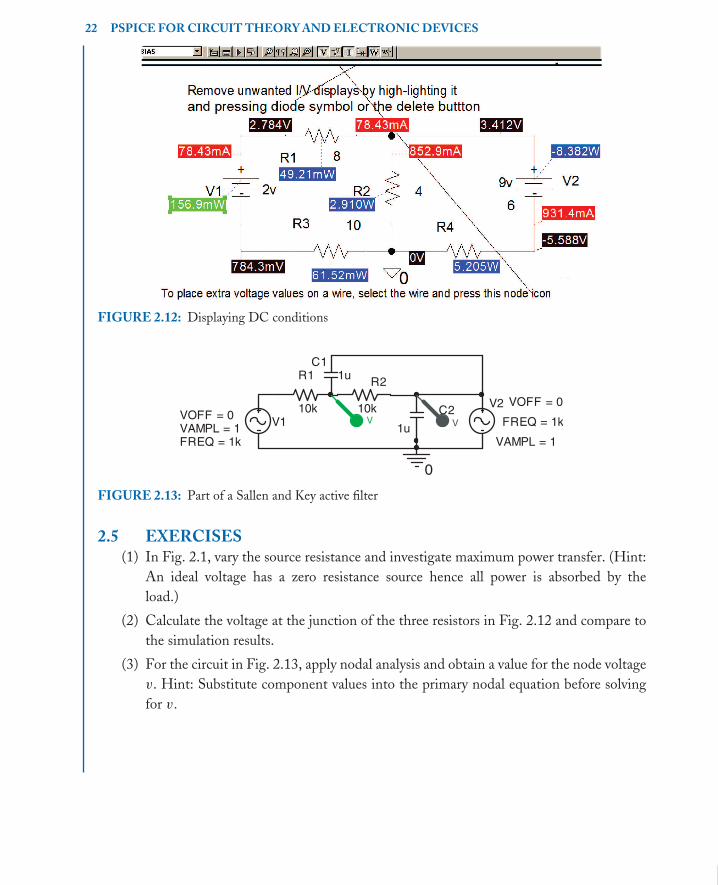
FIGURE 2.10: Changing the digits
Select the PSpice/Bias Points/Preferences menu. Enter 4 in the Displayed Precision
as shown in Fig. 2.11 and it will display the number to four decimal points.
After simulation, select the V/I icons to display DC current and voltages shown in
Fig. 2.12.
To remove redundant voltage or current displays, press the icon to the right of the voltage
or current icons. To add extra voltage displays on a wire, select the wire and press the little node
junction icon beside the main V icon. Make sure Bias Point is ticked in the Analysis Setup
menu.
FIGURE 2.11: Setting the digits
book Mobk059 March 9, 2007 10:21
22 PSPICE FOR CIRCUIT THEORY AND ELECTRONIC DEVICES
FIGURE 2.12: Displaying DC conditions
R1
10k
R2
10k
C11u
C2
1u
0
V2
FREQ = 1k
VAMPL = 1
VOFF = 0
V1
FREQ = 1kVAMPL = 1VOFF = 0
VV
FIGURE 2.13: Part of a Sallen and Key active filter
2.5 EXERCISES(1) In Fig. 2.1, vary the source resistance and investigate maximum power transfer. (Hint:
An ideal voltage has a zero resistance source hence all power is absorbed by the
load.)
(2) Calculate the voltage at the junction of the three resistors in Fig. 2.12 and compare to
the simulation results.
(3) For the circuit in Fig. 2.13, apply nodal analysis and obtain a value for the node voltage
v. Hint: Substitute component values into the primary nodal equation before solving
for v.

book Mobk059 March 9, 2007 10:21
23
C H A P T E R 3
Transient Circuits and LaplaceTransforms
3.1 TRANSIENT ANALYSISComplex signals, such as step or pulse-type signals applied to CR, LR circuits, and LCR
circuits, are analyzed in a much simpler fashion using the Laplace transform (Pierre Laplace
1749–1825). Laplace tables and partial fraction expansion methods are used when transforming
from the s-domain back to the time domain.
3.2 LAPLACE TRANSFORM AND CAPACITANCEThe Laplace Transform of a function f (t) is
LT{ f (t)} = F(s ) =∫ ∞
0
f (t)e−s tdt (3.1)
The current–voltage relationship for a capacitor in the time domain, with an initial voltage
across the capacitor plates V0 (consider this as a step voltage), is
vC (t) =1
C
∫ t
0
i(t)dt + V0 (3.2)
Laplace transforming equation (3.2):
LT{vC (t)} = LT
{
1
C
∫ t
0
i(t)dt + V0
}
(3.3)
The Laplace transform for integration and step functions, is 1/s, hence (3.3) becomes
Vc (s ) =1
s CIc (s ) +
V0
s(3.4)
All transformed circuit variables are shown capitalized in the Laplace equivalent circuit.
Figs. 3.1(a) and 3.1(b) show a capacitor representation in the time and s domains where
the reactance 1/sC I is in series with the initial condition voltage, V0/s, but acting in the sense
shown in Fig. 3.1(b).

book Mobk059 March 9, 2007 10:21
24 PSPICE FOR CIRCUIT THEORY AND ELECTRONIC DEVICES
FIGURE 3.1: Transformed capacitance
3.3 INDUCTANCEThe current–voltage–time relationship for an inductor, with an initial current, I0, is
vL(t) = Ldi
dt+ I0 (3.5)
The Laplace transform of (3.5) is
LT{vL(t)} = VL(s ) = LT
(
Ldi
dt+ I0
)
= s LI (s ) − LI0 (3.6)
An inductor representation in the time domain is shown in Fig. 3.2(a) and the Laplace transform
of an inductor is shown in Fig. 3.2(b) as a reactance sL ohms in series with the initial condition
voltage, LI Volts but in the same direction as the input voltage.
The transformed circuit may also be expressed as a Norton equivalent circuit with the
Norton admittance in parallel with a current source.
3.4 FIRST-ORDER CR AND LR CIRCUITSFigure 3.3 shows a high-pass filter that is used to couple amplifier stages together for the
purposes of DC isolating each stage. A pair of differential markers measures the voltage across
FIGURE 3.2: Transformed inductance

book Mobk059 March 9, 2007 10:21
TRANSIENT CIRCUITS AND LAPLACE TRANSFORMS 25
FIGURE 3.3: High-pass CR circuit
a component that is not connected to the ground reference point, such as the voltage across the
capacitor. Select the PSpice/Markers/ Voltage Differential to place two consecutive markers,
where one marker has a plus symbol and the other has a negative symbol (or use the icons from
the top marker icon toolbar).
Apply the Laplace transform and obtain expressions for the capacitor and resistor voltages.
We may obtain current or voltage expressions in time using the inverse Laplace transform table
given in the appendix. After simulation, compare your calculations to the simulation results for
currents and voltages evaluated at certain times. The Sw tClose switch part from the eval.olb
library is closed at time t = 0 s (Assume the capacitor is initially uncharged). Evaluate the
capacitor voltage at t = 5 s, where V 1 = 10 V, R1 = 2 �, C = 1 F. Capacitance entered in
PSpice as 1 F (no space between the number and the unit) is interpreted as 1 Femto farads—a
much smaller capacitor, so leave out the F symbol.
3.4.1 SolutionThe first switch, sw tClose, closes at a certain time (Note: the sw tOpen switch opens at a
specified time). DLclick the sw tClose part to set the following parameters:
Time to close = TCLOSE = 0 s,
Transient time = TTRAN = 1 us,
Switch resistance when closed = RCLOSED = 0.01 �, and
Switch resistance when opened = ROPEN = 1 Meg
Other mechanical switches are available in the discrete.olb library. The voltage across the
capacitor increases exponentially because the current into the capacitor accumulates charge on
the capacitor plates. The capacitor current, however, decreases exponentially with time because
the capacitor voltage that is building up with time opposes the source voltage. The circuit time
constant, τ = CR, is the time it takes for the capacitor voltage to charge up to 63 % of the applied
step voltage. The time constant is also found by extrapolating the initial slope of the capacitor
voltage with a straight line until it intersects a line drawn across from the final capacitor voltage
to the y-axis. The time constant τ is then measured by dropping a perpendicular line from

book Mobk059 March 9, 2007 10:21
26 PSPICE FOR CIRCUIT THEORY AND ELECTRONIC DEVICES
the intercept to the time axis. The Laplace transform for a step voltage V1 is V1/s , hence the
current is the step voltage divided by the total circuit impedance R+ 1/sC as
IR(s ) =Voltage
Impedance=
10/s
2 + 1/s=
10
2s + 1=
5
s + 1/2=
5
s + 0.5(3.7)
From the Laplace tables, we see that the inverse Laplace transform of 1/(s + a) is e−at , where
a = 0.5 so that Eq. (3.7) when converted to the time domain is 5e−0.5t. The current at t = 5 s
is
iR(t) = 5e−0.5t∣
∣
∣
t=5⇒ iR(5) = 5e−0.5×5 = 5e−2.5 = 0.414 A (3.8)
3.4.2 Partial Fraction ExpansionPartial fraction expansion (PFE) is necessary to transform an equation in s , back to an equation
in time, where the equation in s has no direct equivalent in the Laplace tables. For example,
the capacitor voltage in the previous example is obtained by multiplying the current in (3.8) by
the capacitor reactance to yield
Vc (s ) = I (s )
(
1
s C
)
=(
5
s + 0.5
) (
1
s
)
= 51
(s + 0.5)(s )(3.9)
The two functions 1/(s + 0.5) and 1/s are in the Laplace tables, but the product of the two is
not, so we need to separate the parts using the partial fraction expansion method. The constant
5 is temporarily ignored, so separate the two parts in (3.9) by introducing two new constants A
and B as
1
(s + 0.5)(s )=
A
(s + 0.5)+
B
(s )=
A(s ) + B(s + 0.5)
(s + 0.5)(s )=
(A + B)s + B0.5)
(s + 0.5)(s )(3.10)
Combine all s terms and equate the right and left terms of the top part of (3.10) i.e.
1 = (A + B)(s ) + B0.5 ⇒ (A + B)(s ) = 0 and 0.5B = 1 ⇒ B = 2 (3.11)
Now A + B = 0 since s is not zero and there are no s terms on the LHS of (3.11). This implies
that A = −B = −2. Substitute these values back into (3.10):
Vc (s ) =(
5
s + 0.5
)(
1
s
)
= 51
(s + 0.5)(s )= 5
[
2
s−
2
s + 0.5
]
= 10
[
1
s−
1
s + 0.5
]
(3.12)
The inverse Laplace equivalent for the two parts of (3.12) yields the capacitor voltage in the
time domain as
vc (t) = 10(1 − e−0.5t) V (3.13)

book Mobk059 March 9, 2007 10:21
TRANSIENT CIRCUITS AND LAPLACE TRANSFORMS 27
The capacitor voltage at time t = 5 s is
vc (5) = 10(1 − e−0.5×5) = 10(1 − e−2.5) = 9.17 V (3.14)
3.4.3 Initial ConditionsThere are several methods for setting initial circuit conditions. The Run to time should be set
to at least five time constants in order to display an almost-charged condition on the capacitor.
The first method is to set Analysis type: Time Domain (Transient), Run to time = 15 s,
Maximum step size = 20 ms and tick Skip initial transient solution. This allows PSpice to
charge the capacitor from a zero charge state. The second technique is to select the capacitor and
type in zero volts on an IC parameter (a capacitor parameter). The third technique uses the
IC1 part placed at a junction or the IC2 part placed across the capacitor and a desired voltage
entered. These parts selected from the special.olb library are used to place a final voltage on a
capacitor thus speeding up charging and, hence, simulation times. Press F11 to simulate and
display the voltages across C and R as shown in Fig. 3.4.
FIGURE 3.4: Transient response

book Mobk059 March 9, 2007 10:21
28 PSPICE FOR CIRCUIT THEORY AND ELECTRONIC DEVICES
FIGURE 3.5: The original and Thevenin equivalent circuits
3.5 EXAMPLE 2Fig. 3.5 shows an electrical circuit and the Thevenin equivalent circuit. With C initially
uncharged at time t = 0 s, and switch S1 (Sw tOpen part) closed, the capacitor starts to
charge. Switch S2 (Sw tClose part) is then closed, and S1 opened simultaneously after 3 s.
Obtain an expression, using the Laplace Transform, for the current in C as a function of s
(Hint: Apply Thevenin’s theorem to the left of C , treating C as the load). Obtain an expression
in time for the capacitor voltage and evaluate it at t = 3 s. V 1 = 20 V, R1 = R2 = 4 �,
C = 1 F.
3.5.1 SolutionThe original circuit is simplified by applying Thevenin’s theorem to yield an equivalent resistance
of 2 � because the resistors are now in parallel when you replace the voltage source by a short-
circuit link. In this example, the source is considered an ideal voltage source, and hence has a
zero source resistance. The voltage at the junction of the two resistors to the left of the capacitor
is determined by applying the potential divider principle. Remove the load C . The Thevenin
equivalent voltage is (10/s ) V, i.e. half the input voltage (look up potential divider in the index).
The complete equivalent circuit is shown at the right in Fig. 3.5. The current is calculated by
dividing the Thevenin step voltage by the circuit impedance as
IR(s ) =10/s
2 + 1/s
( s
s
)
=10
2s + 1÷
2
2=
5
s + 1/2=
5
s + 0.5
From the Laplace tables in Appendix A, we convert IR(s ) to current as a function of time
IR(t) = 5e−0.5t

book Mobk059 March 9, 2007 10:21
TRANSIENT CIRCUITS AND LAPLACE TRANSFORMS 29
The current at 3 s is IR(3) = 5e−0.5×3 = 5e−1.5 = 1.11 A. An expression for the capacitor
voltage is obtained by multiplying the current by the capacitor reactance as
Vc (s ) = IR(s )
(
1
s C
)
=(
5
s + 0.5
) (
1
s
)
There are no entries in the Laplace tables for this product, so we need to apply PFE in order
to separate the voltage expression into two functions that are in the tables. For example:
51
(s + 0.5)(s )= 5
(
A
s + 0.5+
B
s
)
= 5
(
A(s ) + B(s + 0.5)
(s + 0.5)(s )
)
= 5
(
(A + B)s + B0.5)
(s + 0.5)(s )
)
To determine A and B, equate the top part of the left-hand side of this equation to the RHS:
1 = (A + B)(s ) + B0.5 ⇒ (A + B)(s ) = 0 ⇒ (A + B) = 0 ⇒ A = −B
This means that 1 = 0.5B ⇒ B = 2
V c (s ) = I (s )
(
1
s C
)
=(
5
s + 0.5
)(
1
s
)
= 5
[
2
s−
2
s + 0.5
]
= 10
[
1
s−
1
s + 0.5
]
From the Laplace tables, we see that 1/s is equivalent to 1 in the time domain and 1/(s + 0.5)
is equivalent to e−0.5t . The capacitor voltage in the time domain is
vc (t) = 10(1 − e−0.5t) V
At t = 3 s, the 20 V supply is disconnected by opening S1 and closing S2, thus allowing the
capacitor to charge to vc (3) = 10(1 − e−0.5×3) = 7.76 V. The circuit now comprises a voltage
source 7.76/s V in series with a 2 � resistance and a 1 F capacitor. However, this voltage source is
not a constant voltage supply and so decays exponentially vc (t) = 10e−0.5t . The current changes
direction instantaneously because the capacitor cannot charge instantaneously but decays in an
exponential manner. Select the Analysis/Transient menu and set Run to time to 15 s and
Maximum step size (default value). Press F11 to simulate and produce the current and voltage
waveforms shown in Fig. 3.6.
3.6 EXAMPLE 3Fig. 3.7 shows a switch open for a long time which is then closed at t = 0.2 s. Obtain
an expression for the inductor current as a function of s . Using the Laplace tables, get an
expression for the inductor current in time and evaluate at t = 0, 0.2 and 0.3 s. Assume zero
initial conditions and R1 = R2 = 5 �, L = 2 H, V1 = 1 V.

book Mobk059 March 9, 2007 10:21
30 PSPICE FOR CIRCUIT THEORY AND ELECTRONIC DEVICES
FIGURE 3.6: Current and voltage waveforms
3.6.1 SolutionLaplace transforming the circuit yields the current as
IL(s ) =1/s
2s + 10=
1
s
1
2s + 10=
1
(s )
1/2
(s + 5)= 0.5
[
1
(s )(s + 5)
]
=A
s+
B
s + 5
V1 1
+
-
U1 TCLOSE = 0.2s1 2
R1 5 R2 5
L1 2
0
I
V
FIGURE 3.7: Switch closed at 0.2 s

book Mobk059 March 9, 2007 10:21
TRANSIENT CIRCUITS AND LAPLACE TRANSFORMS 31
FIGURE 3.8: Inductor current
Ignore the 0.5 factor and equate the top left-hand side of the equation to the right-hand side as
1 = (A + B)(s ) + A5 ⇒ A = 1/5 and (A + B)(s ) = 0 ⇒ (A + B) = 0, or, B = −A = −1/5
Another method of solving PFE coefficients is [ 1s +5 ]S=0 ⇒ A = 1
5 and [ 1s ]S=−5 ⇒ B = − 1
5
IL(s ) = 0.5
[
1/5
s−
1/5
s + 5
]
=0.5
5
[
1
s−
1
s + 5
]
= 0.1(1 − e−5t)
The current at t = 0.2 s is i = 63 mA (see Fig. 3.8). Closing the switch at t = 0.2 s reduces
the circuit resistance to 5 �, However, the inductor initial voltage is now equal to the current at
0.2 s multiplied by the inductance, i.e. VL = I (0.2)L = (63 mA)(2 Henries) = 0.106 V. The
initial voltage direction is in the opposite direction to the voltage drop across the inductance.
The current is the voltage (1/s + 0.106)/impedance i.e.
IL(s ) =1/s + 0.126
2s + 5=
1/2s
s + 2.5+
0.063
s + 2.5=
0.5
(s )(s + 2.5)+
0.063
s + 2.5

book Mobk059 March 9, 2007 10:21
32 PSPICE FOR CIRCUIT THEORY AND ELECTRONIC DEVICES
Apply partial fraction expansion to the first part 1(s )(s +2.5) = [ A
s + Bs +2.5 ] and solve
[
1
s + 2.5
]
S=0
⇒ A =1
2.5and
[
1
s
]
S=−2.5
⇒ B = −1
2.5
IL(s ) = 0.5
[
1/2.5
s−
1/2.5
s + 2.5
]
+0.063
s + 2.5=
.5
2.5
[
1
s−
1
s + 2.5
]
+0.063
s + 2.5
This current as a function of time is written from the Laplace tables as
IL(t) = 0.2(1 − e−2.5t) + 0.063e−2.5t mA
Note: We evaluate this last expression at t = 0.3 s by substituting the elapsed time of 0.1 s =(0.3 s–0.2 s), and not 0.3 s, which is the total time.
IL(0.1) = 0.2(1 − e−2.5×0.1) + 0.063e−2.5×0.1 = 92 mA
Set Run to time = 3 s, Maximum step size = 500 u. Press F11 to simulate to display the
inductor current in Fig. 3.8.
Note the inductor voltage has a distinct discontinuity at the time of switching.
3.7 EXAMPLE 4The switch in Fig. 3.9 is initially opened and then closed at t = 80 ms. Using the Laplace
transform, obtain an expression in s for the inductor current. Hence, calculate a value for
the inductor current at t = 80 ms. Assume the inductor is initially uncharged. R1 = 5 �,
R2 = 20 �, L = 0.1 H, I1 = 2 A, I2 = 3 A.
FIGURE 3.9: Problem 4 using parallel current sources

book Mobk059 March 9, 2007 10:21
TRANSIENT CIRCUITS AND LAPLACE TRANSFORMS 33
3.7.1 SolutionBefore the switch is closed, calculate the inductor current by applying the current divider
principle to I1, R2, and L1:
IL(s ) =2
s
20
20 + s 0.1=
(
2
s
) (
200
200 + s
)
=400
s
1
(200 + s )= 400
[
A
s+
B
s + 200
]
Solve for A and B using partial fraction expansion [ 1s +200 ]s =0 ⇒ A = 1
200 and [ 1s ]s =−200 ⇒
B = − 1200 .
IL(s ) =400
200
[
1 −1
s + 200
]
⇒ IL(t) = 2[
1 − e−200t]
A
When the switch is closed at t = 80 ms, the inductor current is IL(80 ms) = 2(1 −e−200×80ms) = 2 A. The initial inductor current I0 produces a back EMF I0 = 80 mV. The
equivalent circuit is a generator in series with the inductor reactance. Complete the solution
by combining the two current sources into one source and the two resistances into one resis-
tance. Set Analysis to Analysis type: Time Domain (Transient), Run to time = 500 ms, and
Maximum step size = 10 us. Press F11 to plot the inductor current shown in Fig. 3.10.
FIGURE 3.10: Inductor current

book Mobk059 March 9, 2007 10:21
34 PSPICE FOR CIRCUIT THEORY AND ELECTRONIC DEVICES
C110u
R1
1k
V3 1V
+
-
V115
+
-
L1
1
R5
5
V4 1
+
-
L2
2
U1
TOPEN = 0.02
1 2
V5
2v
+
-
V7
.67
+
-
V6
.67
+
-
U3
TCLOSE = 0.2
1 2
U7
TOPEN = 0.75ms
1 2
U6
TCLOSE = 0.75ms
1
2 R9
2.5
V81
+
-
C2 1
R65
R2 5k
U2TCLOSE = 0.02
1
2
U5
TCLOSE = 0
1 2
V2 1V
+
-
U8
TCLOSE = 2 1 2
C3
1
R8
2.5
R31 R41
U4
TCLOSE = 0.1
1 2
R7
0.133m
0
0 00
0
I
I
I
V
I V
FIGURE 3.11: Switching circuits
3.8 EXERCISE(1) Investigate the transient exercises shown in Fig. 3.11.

book Mobk059 March 9, 2007 10:21
35
C H A P T E R 4
Transfer Functions and SystemParameters
4.1 TRANSFER FUNCTIONSA transfer function comprises numerator and denominator parts with each part containing one
or more factors. We may use a LAPLACE part to plot the transfer function frequency response
or the impulse response. The default Laplace part has a unity numerator and denominator is
1 + s, which is a low-pass filter with a 1 rs−1 cut-off frequency. Each transfer function factor
entered is separated by a multiplier operator “*”. For example, if the numerator is 5 s, then enter
it as 5*s. A fourth-order polynomial, factored into two second-order polynomials, has each
polynomial enclosed by brackets () but separated by a “*” symbol between each pair of brackets.
4.2 BUTTERWORTH TRANSFER FUNCTIONS AND THELAPLACE PART
A second-order transfer function is formed from an inverted second-order Butterworth
loss function with a cut-off frequency ω20 = 100 ⇒ ω0 = 10 rs−1 ⇒ f0 = 10 rs−1/(2π ) =
1.59 Hz. The Butterworth loss function is de-normalized by replacing the normalized complex
frequency variable $ with the complex frequency variable, s , divided by the cut-off frequency
[ref: 1]. The transfer function is therefore
H(s ) =Vout
Vin=
1
$2 + 1.414$ + 1
∣
∣
∣
∣
$=s /10
=1
( s10 )2 + 1.414 s
10 + 1=
100
s 2 + 14.14s + 100(4.1)
Draw the schematic in Fig. 4.1 and use the Net Alias icon to place a name on the output wire.
Select the Laplace part, Rclick and select Edit Properties. In the DENOMinator box,
enter the transfer function denominator (s ∗s + 14.14∗s + 100), and 100 in the NUMerator
box. In the top right-hand corner press the small x to exit the properties. To plot the frequency
response, place a dB marker (From the PSpice/Markers/Advanced menu) on the output port.
From the Analysis Setup menu, set the sweep parameters shown in Fig. 4.2 to plot 1001 points
for each decade in the response from 0.1 Hz to 10 kHz.
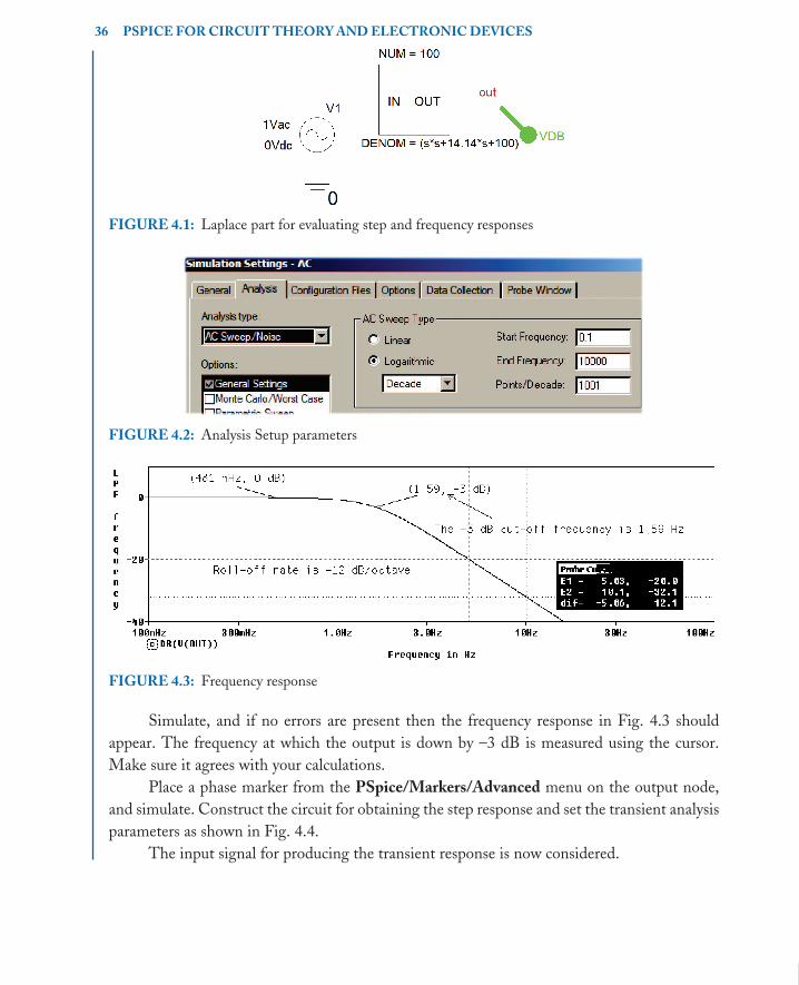
book Mobk059 March 9, 2007 10:21
36 PSPICE FOR CIRCUIT THEORY AND ELECTRONIC DEVICES
FIGURE 4.1: Laplace part for evaluating step and frequency responses
FIGURE 4.2: Analysis Setup parameters
FIGURE 4.3: Frequency response
Simulate, and if no errors are present then the frequency response in Fig. 4.3 should
appear. The frequency at which the output is down by –3 dB is measured using the cursor.
Make sure it agrees with your calculations.
Place a phase marker from the PSpice/Markers/Advanced menu on the output node,
and simulate. Construct the circuit for obtaining the step response and set the transient analysis
parameters as shown in Fig. 4.4.
The input signal for producing the transient response is now considered.

book Mobk059 March 9, 2007 10:21
TRANSFER FUNCTIONS AND SYSTEM PARAMETERS 37
FIGURE 4.4: Transient analysis parameters
FIGURE 4.5: Step response testing
4.2.1 Piece-wise Linear Part (VPWL)A piece-wise linear (VPWL) shown in Fig. 4.5, part generates a unit step function whose
parameters are displayed on the schematic. Alternatively, use a VDC part as a step voltage
source.
The step response in Fig. 4.6 shows the step response as an exponentially decaying
sinusoidal signal. Separate the input and output signals using Alt PP, Ctrl X, Ctrl V on a
variable selected at the bottom left of the Probe output.
4.3 PROBE GRID AND CURSORS ICONSThe function of each cursor icon is given in a little information box that pops up when you
place the mouse cursor on each one as shown in Fig. 4.7. To place specific values on a plot,
turn on the cursor, select the maximum-value icon (fifth one from the left) to place intersecting
cursors at the maximum value.

book Mobk059 March 9, 2007 10:21
38 PSPICE FOR CIRCUIT THEORY AND ELECTRONIC DEVICES
FIGURE 4.6: Unit step response
FIGURE 4.7: Probe cursor icons
Pressing the second last icon on the right places a pair of x and y values at the largest
value location. This may be repeated for other peaks by pressing the maximum value icon again
and pressing the second last icon, where it places another pair of x and y values at the second
largest value, and so on.
The percentage overshoot (PO), is the maximum value minus the step value divided
by the step value and multiplied by 100 %. For a unit step, the overshoot is the maximum
value of the step response minus one and then multiplied by 100 %. So, in this case it is
(1.0429-1)*100 % = 4.29 % (see Section 4.9).
4.4 ELAPLACE PART AND THE STEP RESPONSEWe can measure system parameters such as rise time and steady-state values by applying
a step signal and measuring different parameters from the step response. In second-order
systems, we measure overshoot, settling time and natural frequency from the step response.
The ELAPLACE part in Fig. 4.8 can be used to obtain step and impulse responses by entering
the transfer function into the XFORM box.

book Mobk059 March 9, 2007 10:21
TRANSFER FUNCTIONS AND SYSTEM PARAMETERS 39
FIGURE 4.8: The Elaplace part
FIGURE 4.9: VPWL step generator spreadsheet
A low-pass filter transfer function, with a cut-off frequency 1000 r/s ( fc = 159 Hz), is
expressed as
H(s ) =Vout
Vin=
ωp
s + ωp
∣
∣
∣
∣
ω=1000
=1000
s + 1000(4.2)
Select the VPWL generator part, Rclick and select Edit Properties and enter the parameter as
shown in Fig. 4.9. This creates a step function with the voltage, at time t1 = 0 s, equal to 10 V.
Rclick the ELAPLACE and select Edit Properties to display the part properties shown
in Fig. 4.10. Enter the transfer function 100/(s+100) in the A column of the XFORM row.

book Mobk059 March 9, 2007 10:21
40 PSPICE FOR CIRCUIT THEORY AND ELECTRONIC DEVICES
FIGURE 4.10: Elaplace part parameter spreadsheet
FIGURE 4.11: Transient Analysis parameters
Terminate the ELAPLACE output with a port left part from the right-hand menu and
set the Transient Analysis parameters as shown in Fig. 4.11.
Press the simulate icon (Or the F11 key), and the step response in Fig. 4.12 should
appear.
We will show in Section 4.9 how to measure the rise time.
4.5 CHEBYCHEV TRANSFER FUNCTIONS IMPULSE RESPONSEA second-order Chebychev loss function with 2 dB ripple (ε = 0.746) in the passband is
$2 + 0.804$ + 0.823. Invert this function and denormalize by replacing $ with s /1000 to
produce the following transfer function:
H(s ) =Vout
Vin=
1
$2 + 0.804$ + 0.823
∣
∣
∣
∣
$=s /1000
=106
s 2 + 804s + 823.103(4.3)

book Mobk059 March 9, 2007 10:21
TRANSFER FUNCTIONS AND SYSTEM PARAMETERS 41
FIGURE 4.12: First-order step response
FIGURE 4.13: Impulse parameters
The maximum response occurs at the resonant frequency.
ω20 = 823 krs−1 ⇒ f0 = (
√
ω20)/2π =
√823 kr−1
/2π = 145 Hz
However, this is not the same as the passband edge frequency. The gain at DC is
1 Meg/0.823 Meg = 1.21. Fig. 4.13 shows an ELAPLACE part with the transfer func-
tion entered in the XFORM as 1e6/(s ∗s + 804∗s + 823K). Select the VPWL part and enter
the impulse input signal parameters to produce a 10 V pulse with a width of 2 us.
Set Analysis to Analysis type: Time Domain (Transient), Run to time = 100 ms, and
Maximum step size = 1 us. Press F11 to simulate. Separate the overlapping displays by creating
two more extra plots using the Alt PP buttons twice. Delete and select the output variable you
wish to move by selecting the V(out) variable and pressing the Ctrl X buttons. Paste the copied
variable into the new plot with Ctrl V.

book Mobk059 March 9, 2007 10:21
42 PSPICE FOR CIRCUIT THEORY AND ELECTRONIC DEVICES
FIGURE 4.14: Impulse and frequency response
4.5.1 Unsynchronizing Probe PlotsOn the top plot, select Plot/Unsyncronize X-Axis and press the FFT icon. Unsynchronizing
the x-axis enables us to plot the frequency response but keep the other plots still in the time
domain as shown in Fig. 4.14. You might need to increase the transient Run to time to 1 s in
the analysis setup to achieve good frequency resolution.
Measure the frequency at the max of the display and the time between peaks in the
middle plot (verify it is equal to 1/ f 0). Measure the overshoot, settling time, and natural
frequency. There is an error at the beginning of the frequency response but see Section 4.7 for
an explanation.
4.6 FIRST-ORDER LOW-PASS FILTER STEP AND IMPULSERESPONSES
Impulse testing is useful for assessing system stability. An impulse is created using the VPULSE
part by setting the period much larger compared to the pulse width as shown in Fig. 4.15, where
the impulse is 10 ns wide and the period is 10 s.

book Mobk059 March 9, 2007 10:21
TRANSFER FUNCTIONS AND SYSTEM PARAMETERS 43
FIGURE 4.15: LPF
FIGURE 4.16: Vpulse generator parameters
FIGURE 4.17: Transient analysis parameters
Enter the VPULSE generator parameters shown in Fig. 4.16 and set the Transient
Analysis as shown in Fig. 4.17.
Transient Analysis parameters are shown in Fig. 4.17. After simulation, create separate
display using Alt PP and place the output signal on top by applying Ctrl X on the selected
output variable at the bottom left of the Probe output. The x-axis range is changed from a
Run to time of 15 ms to 10 us so that the impulse signal and response can be observed clearly,
as shown in Fig. 4.18.

book Mobk059 March 9, 2007 10:21
44 PSPICE FOR CIRCUIT THEORY AND ELECTRONIC DEVICES
FIGURE 4.18: The impulse response
FIGURE 4.19: Frequency response
4.7 OBTAINING THE FREQUENCY RESPONSE FROM THEIMPULSE RESPONSE
The Fast Fourier Transform (FFT) icon displays the frequencies contained in a complex signal
but is also useful for obtaining the frequency response from the impulse response. The amplitude
frequency response in Fig. 4.19 was obtained from the impulse response by selecting the FFT
icon from the Probe screen toolbar. In this experiment, we wish to obtain the frequency response

book Mobk059 March 9, 2007 10:21
TRANSFER FUNCTIONS AND SYSTEM PARAMETERS 45
FIGURE 4.20: Changing the x-axis
for the low-pass filter by applying an impulse to the circuit. However, a small error will occur at
the beginning of the frequency response. Run to time = 15 ms results in the incorrect display
from 0 Hz to 66.66 Hz (66 Hz = 1/15 ms).
Making the Run to time larger increases the resolution in the frequency domain and also
reduces the error at the start. Change the frequency axis by selecting an x-axis number and
setting the parameters as shown in Fig. 4.20.
We should remember this technique when we cannot carry out a normal ac frequency
response, for example, when a circuit contains switch components, such as in a switched
capacitor circuit, and requires a transient analysis [ref: 1].
4.8 THE LOW-PASS C R FILTER STEP RESPONSEFrom the step response, we may determine system parameters, such as rise time, and steady-
state value. In second-order systems, we may measure overshoot, settling time, and natural
frequency. Draw the schematic shown in Fig. 4.21 using a VDC part to provide a step input
signal.
From Analysis/Transient Analysis menu, tick Skip initial transient solution and set
the Run to time to 1 ms. If we use a VPULSE generator instead of the VDC part, then make
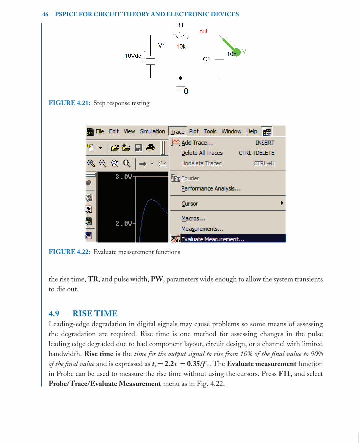
book Mobk059 March 9, 2007 10:21
46 PSPICE FOR CIRCUIT THEORY AND ELECTRONIC DEVICES
FIGURE 4.21: Step response testing
FIGURE 4.22: Evaluate measurement functions
the rise time, TR, and pulse width, PW, parameters wide enough to allow the system transients
to die out.
4.9 RISE TIMELeading-edge degradation in digital signals may cause problems so some means of assessing
the degradation are required. Rise time is one method for assessing changes in the pulse
leading edge degraded due to bad component layout, circuit design, or a channel with limited
bandwidth. Rise time is the time for the output signal to rise from 10% of the final value to 90%
of the final value and is expressed as tr = 2.2τ = 0.35/f c . The Evaluate measurement function
in Probe can be used to measure the rise time without using the cursors. Press F11, and select
Probe/Trace/Evaluate Measurement menu as in Fig. 4.22.

book Mobk059 March 9, 2007 10:21
TRANSFER FUNCTIONS AND SYSTEM PARAMETERS 47
FIGURE 4.23: Evaluate measurement functions
FIGURE 4.24: Rise-time measurement using Evaluate Measurement function
Select Risetime (1) from the list of functions in Fig. 4.23 to place it in the Trace
Expression box.
Replace the default “1” value in the function brackets with the capacitor voltage V(out)
function, selected from the list on the left. Fig. 4.24 shows the Evaluate Measurement function
evaluated at the bottom as 10% final value to 90% final value equal to tr = 2.2τ = 2.2 C R =2.2∗1e4∗10e − 9 = 219 us.

book Mobk059 March 9, 2007 10:21
48 PSPICE FOR CIRCUIT THEORY AND ELECTRONIC DEVICES
FIGURE 4.25: Second-order LCR circuit
4.10 STEP RESPONSE OF A SERIES-TUNED LCR CIRCUITThe second-order resonant LCR circuit in Fig. 4.25 investigates “circuit damping” by varying
the circuit resistance and observing the waveforms. Select the resistance and change the default
1 k� to {Rvar} (brackets included).
A PARAM part defines Name1 = RVAR for the resistance, and Value1 = 1. From the
Analysis Setup menu, select Parametric, and set Name to RVAR. Set Start Value = 20 �,
End Value = 200 � and a 60 � resistance increment. Set the Analysis tab to Analysis type:
Time Domain (Transient), Run to time = 15 ms, and Maximum step size = 1 us. After
pressing F11 to simulate, a small screen of Available Sections will appear, so select OK, or
press the ENTER button. The range of damping from underdamped to overdamp is shown in
the step response in Fig. 4.26.
4.10.1 OvershootOvershoot is a measure of the step response of a circuit. When a circuit is underdamped
the output rises to a maximum of 1.38 V, an excess of 0.38 V for a 1 V step. Use the
Probe/Trace/Evaluate Measurement Functions in Probe to measure all parameters. For
example, the overshoot function: Overshoot(V(C1:2)), yields an over shoot of 38% as shown at
the bottom of Fig. 4.26. You should also notice at the bottom of the display symbols representing
each trace. Selecting any one of these symbols shows the information for a particular value of
the swept variable.
4.11 EXERCISES(1) Use an ABM E part to create the integrator in Fig. 4.27. The input data is applied
using a VPWL part, or a VPULSE part with ±1 V amplitude, PW =1 ns, and PER
= 2 n. Here, τ = CR = 1 k� × 2 pF = 2 ns.
(2) An oscilloscope probe reduces the effect of the input oscilloscope capacitance on a
signal. Without such a probe, a step or pulse signal has the rise time degraded. The
10:1 oscilloscope probe in Fig. 4.28 is calibrated by attaching the probe end onto the

book Mobk059 March 9, 2007 10:21
TRANSFER FUNCTIONS AND SYSTEM PARAMETERS 49
FIGURE 4.26: Range of damping coefficients
FIGURE 4.27: Integration using the E part
reference square wave signal on the front panel of the oscilloscope. In normal usage,
the probe tip variable capacitance is adjusted by inserting a small plastic trimming
tool and adjusting it to produce the best displayed square wave. The best display is
where the applied signal looks like the original reference but reduced in amplitude by a
factor of 10.

book Mobk059 March 9, 2007 10:21
50 PSPICE FOR CIRCUIT THEORY AND ELECTRONIC DEVICES
Rl
1meg
Rs
50
Vstep
V1 = 0
V2 = 1
TR = 1p
TF = 1p
PER = 1
PW = 0.1
+-
PARAMETER
CVAR = 11p
Rtip 9meg
Ctip {cvar}
Cl
100pF
0Oscilloscope 10by 1 probe
V
FIGURE 4.28: Oscilloscope probe
FIGURE 4.29: Different values of Cvar
This is simulated in PSpice using a PARAM part to vary Ctip from 1 pF to 30 pF
in steps of 1 pF. Use the Evaluate Measurement function Risetime (V (Cl:1)) from
the list. Determine from Fig. 4.29, the best value for cvar. The best value occurs when
the displayed scope signal is a square wave (This occurs when the output voltage is
one tenth of the input voltage—hence the probe name). A useful exercise is to plot the

book Mobk059 March 9, 2007 10:21
TRANSFER FUNCTIONS AND SYSTEM PARAMETERS 51
FIGURE 4.30: RMS meter in block form
FIGURE 4.31: Comparison of Probe function RMS () to the RMS meter
frequency response for this Probe circuit using a VAC part and run an AC analysis for
the different cvar capacitor values. What should you observe (high-pass or low-pass
response?)
(3) The true RMS meter in Fig. 4.30 is constructed from ABM parts (GVALUE and
EVALUE). Apply a 1 kHz, 1 V sinusoidal signal using a VSIN part. To square the
input voltage, enter EXP = V(in)*V(in), or (V(in)**2) into the GVALUE part. The
integrator is followed by an EVALUE part using the IF then ELSE statement as: IF
(TIME<=0, 0, sqrt(V(1)/TIME)). This avoids convergence problems, but also gets
the square root of the voltage on the wire labeled 1. Run a transient analysis for 50 ms.
Fig. 4.31 compares the RMS output to the probe function RMS (V(RMSout)). Both
eventually settle down to the same output voltage of 0.707 V.

book Mobk059 March 9, 2007 10:21
52 PSPICE FOR CIRCUIT THEORY AND ELECTRONIC DEVICES
(4) Repeat the previous exercise for a pulse waveform. The power of a pulse waveform is
P =1
T
τ∫
0
V 2
Rdt =
1
T R(V 2t)τ0 =
τ
T
V 2
RW (4.4)
The RMS value is
VRMS =√
τ
TV V (4.5)
Note: For a square wave τ = T/2, so the RMS value is V/√
2—the same as a pure
sinusoidal signal.

book Mobk059 March 9, 2007 10:21
53
C H A P T E R 5
AC Circuits and Circuit Theorems
5.1 AC CIRCUIT THEORYCapacitors and inductors have frequency-dependant reactive properties making them useful
for modifying the frequency content of signals. In this chapter, we apply circuit theorems to
a range of circuits such as series and parallel resonant circuits used in many communication
circuits where important concepts, such as selectivity and Q-factor are examined.
5.2 CAPACITORSTwo metal plates of area of A and separated by an insulator thickness d and absolute permittivity
ε has capacitance:
C =εA
d(5.1)
Connecting a voltage V across a capacitor deposits a charge, Q coulombs, on its plates
(Charles Coulomb 1738–1806). Since current is proportional to the rate of change of charge
with time and Q = C V , therefore
i =d Q
dt= C
d V
dt(5.2)
A voltage Vc (t) = Vm sin ωt across a capacitor C produces current that leads the voltage by 90◦.
i = Cd Vc
dt= C
d (Vm sin ωt)
dt= ωC Vm cos ωt =
Vm
1/ωCcos ωt =
Vm
XCcos ωt = Im cos ωt
(5.3)
Rearranging (5.3) yields the capacitive reactance:
XC = Vm/Im = 1/ωC � (5.4)
Capacitive reactance decreases with frequency increase and is an open circuit at DC. We may
express the current–voltage relationship as susceptance and is the reciprocal of reactance defined
as Bc = Im/Vm = ωC Siemens.

book Mobk059 March 9, 2007 10:21
54 PSPICE FOR CIRCUIT THEORY AND ELECTRONIC DEVICES
FIGURE 5.1: Capacitive reactance
5.2.1 Capacitive Reactance PlotCapacitive reactance is investigated using the schematic in Fig. 5.1, where a VAC generator
part is connected to the capacitor via a small resistance that represents the source resistance of
the voltage source.
Set the Analysis tab to Analysis type: AC Sweep/Noise, AC Sweep Type to Linear,
Start Frequency = 0.01, End Frequency = 10, Points/Decade = 10,000 (this large value
gives a smoother reactance plot). There are two techniques for plotting signals in Probe. The
first technique is to place markers on the schematic, which, after simulation, automatically
plots the required voltage or current waveforms. The second technique uses no markers but the
variables are selected after pressing the Trace/ Add Trace menu from the Probe screen shown
in Fig. 5.2.
Alternatively, press the Insert button and in Trace Expression box, select the variables
V(C: 2)/I(C) from the list to plot positive capacitive reactance. When the plot shown in
Fig. 5.4, select an x-axis parameter or the space beside it, and it will open the menu shown in
Fig. 5.3.
Change the Scale to Log and add a title by selecting Use this title and typing a name in
the Axis Title box.
FIGURE 5.2: Select the voltage variable

book Mobk059 March 9, 2007 10:21
AC CIRCUITS AND CIRCUIT THEOREMS 55
FIGURE 5.3: Changing the x-axis to logarithmic
5.2.2 Capacitor Current and Voltage WaveformsTo observe the phase relationships between the capacitor current and voltage, we need to carry
out a transient analysis and measure the time between the peak values. The VAC generator is
replaced by a VSIN generator whose parameters are shown in Table 5.1.
Enter the VSIN generator parameters: VOFF = 0, VAMPL = 1 and FREQ = 10.
Set the Analysis tab to Analysis type: Time Domain (Transient), Run to time = 0.2, and
FIGURE 5.4: Capacitive reactance

book Mobk059 March 9, 2007 10:21
56 PSPICE FOR CIRCUIT THEORY AND ELECTRONIC DEVICES
TABLE 5.1: VSIN Parameters
PARAMETER MEANING
AC Voltage amplitude
VOFF Offset voltage
VAMPL Peak voltage value
FREQ Frequency
TD Delay
DF Damping factor
PHASE Phase
Maximum step size = 100 us. The coarseness of the plot depends on the Maximum step size
which should be decreased whenever you observe triangulation, or straight lines, where they
should be curved. To plot microamps and volts on the same plot, requires adding a different
y-axis for each signal, otherwise the current signal will appear to be zero. This is fixed by adding
a new Y -axis from the Plot menu and selecting Add Y Axis (or Ctrl Y). Select the left-hand
side of the inner vertical Y -axis and you should see the Y-axis number is 2.
Double chevrons ≫ on the y-axis indicates which axis is selected. From the Trace menu,
select Add, or press the icon and insert the capacitor voltage V(C:2) in the Trace Expression
box. Lclick on the left-hand side of the outer vertical y-axis (The added axis), and observe
the Y-axis number is 1. Press the insert button (or select the insert icon) and select the I(C1)
variable. Two variables should now be displayed as shown in Fig. 5.5. The phase difference
between current and voltage signals is determined indirectly using cursors to measure the time
difference, 1t, between the two selected signals and converted to degrees using the following
expression:
T
360=
1t
θ⇒ θ =
360.1t
T=
360.25 ms
100 ms= 90◦ (5.5)
T is the period of the signal (equal to 100 ms for a 10 Hz a sinusoid) and has a phase of 2π
(360◦).
5.3 INDUCTORSThe current and voltage in an inductor (Michael Faraday 1791–1867) are related:
E = Ldi
dt(5.6)
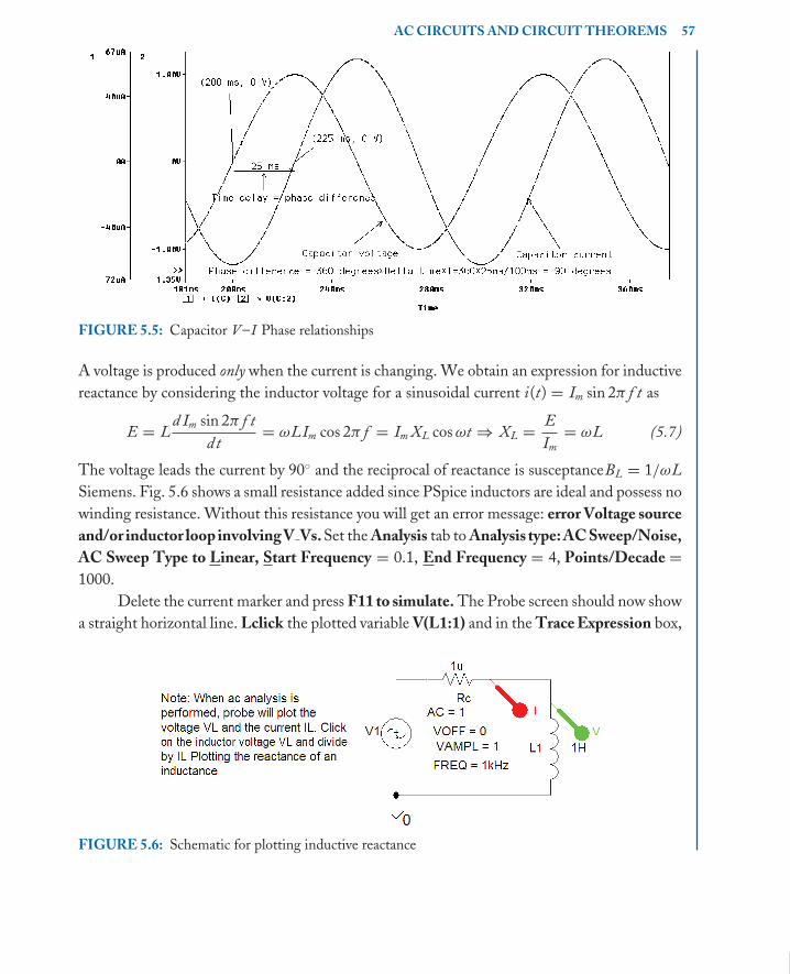
book Mobk059 March 9, 2007 10:21
AC CIRCUITS AND CIRCUIT THEOREMS 57
FIGURE 5.5: Capacitor V –I Phase relationships
A voltage is produced only when the current is changing. We obtain an expression for inductive
reactance by considering the inductor voltage for a sinusoidal current i(t) = Im sin 2π f t as
E = Ld Im sin 2π f t
dt= ωLIm cos 2π f = Im XL cos ωt ⇒ XL =
E
Im= ωL (5.7)
The voltage leads the current by 90◦ and the reciprocal of reactance is susceptanceBL = 1/ωL
Siemens. Fig. 5.6 shows a small resistance added since PSpice inductors are ideal and possess no
winding resistance. Without this resistance you will get an error message: error Voltage source
and/or inductor loop involving V Vs. Set the Analysis tab to Analysis type: AC Sweep/Noise,
AC Sweep Type to Linear, Start Frequency = 0.1, End Frequency = 4, Points/Decade =1000.
Delete the current marker and press F11 to simulate. The Probe screen should now show
a straight horizontal line. Lclick the plotted variable V(L1:1) and in the Trace Expression box,
FIGURE 5.6: Schematic for plotting inductive reactance

book Mobk059 March 9, 2007 10:21
58 PSPICE FOR CIRCUIT THEORY AND ELECTRONIC DEVICES
FIGURE 5.7: Inductive reactance plot
divide the variable by the inductor current i.e. V(L1:1)/I(L1). Change x-axis Scale to Linear
scale by selecting the log/lin icon. This makes the inductive reactance ωL plotted as a linear
increase with frequency shown in Fig. 5.7. The impedance of an ideal inductor (Joseph Henry
1797–1878) is zero at zero frequency (DC) and is an open circuit at infinity frequency.
5.3.1 Inductor Signal Phase MeasurementPlace a current marker on the output. Set the Analysis tab to Analysis type: Time Domain
(Transient), Run to time = 10 ms, and Maximum step size = 1 us. Press F11 to simulate and
display the inductor current and voltage, as shown in Fig. 5.8. However, it is necessary to use
the previous procedure for measuring capacitor V –I phase relationships i.e. in Probe, add a
new axis (Ctrl Y) in order to display the current with an appropriate range.
The phase difference between current and voltage signals is determined indirectly using
cursors to measure the time difference, 1t, between the two selected signals and converted to
degrees using the following expression:
T
360=
1t
θ⇒ θ =
360 × 1t
T=
360 × 250u
1000us= 90◦ (5.8)
The period T is 1 ms for a 1 kHz a sinusoid equal to a phase of 2π360◦.
5.4 AC CIRCUIT THEOREMSThevenin’s theorem (Leon Thevenin 1857–1926) states that any two-terminal circuit may be
replaced by an equivalent circuit comprising an impedance measured across the open-circuit

book Mobk059 March 9, 2007 10:21
AC CIRCUITS AND CIRCUIT THEOREMS 59
FIGURE 5.8: Inductor V –I phase plot
output determinals, but with all sources replaced by their internal impedances, and placed in
series with the voltage measured across the output terminals when open circuited.
5.4.1 Thevenin’s TheoremThe large value resistance ZL in Fig. 5.9 represents an open-circuit load in order to measure
values for the Thevenin equivalent circuit. Apply a 10 V VAC part and measure the current
and voltage in each loop using the IPRINT and VPRINT parts (a printer symbol). Loop
currents are logged by ammeters, mesh1, and mesh2 and the measurements from these virtual
instruments are contained in an output file accessed from the PSpice/View Output File menu
(see Fig. 5.13).
DLclick the AC voltage source V 1, and enter 10 V and phase angle = 0 in the Edit
Properties spreadsheet. Vprint1 (A printer symbol in the special.olb library) is used to record
voltage values in the Output file. Select the meter and enter the Vprint1 voltmeter parameters
FIGURE 5.9: Two-loop circuit

book Mobk059 March 9, 2007 10:21
60 PSPICE FOR CIRCUIT THEORY AND ELECTRONIC DEVICES
FIGURE 5.10: The VPRINT1 parameters
as shown in the spreadsheet shown in Fig. 5.10. Type ok, or y, beside a parameter you wish
displayed in the output file.
The IPRINT1 part measures the current in each loop, and is placed in series with a
component. Select the part and fill in the required parameters as per the VPRINT part. Specify
the ammeter parameters by typing ok beside each parameter required in the output file. Set the
Analysis tab to Analysis type: AC Sweep/Noise, AC Sweep Type to Linear, Start Frequency
= 100, End Frequency = 100, Points/Decade = 1. The analysis is carried out when the start
and end frequencies are equal, i.e. at one frequency only. In this example, the capacitance C1
has a reactance of 200 � at a frequency of 100 Hz.
5.4.2 Thevenin ImpedanceApply Thevenin’s theorem to the left of the load ZL, which is a large resistance (10 Meg)
representing an open circuit. Create the equivalent circuit and place it on the same schematic
area. Replacing ZL with the complex conjugate of the Thevenin impedance ensures maximum
power transfer between the circuit and the load. The Thevenin impedance is R2 in series with
R1 in parallel with Xc 1. Replace the V 1 supply with its internal resistance, which is zero.
ZTH = R2 +R1(− j XC1)
R1 − j XC1= 20 +
100(− j200)
100 − j200= 100 − j40 � (5.9)
Maximum power is transferred when the load is equal to the complex conjugate of the Thevenin
impedance. The load impedance for maximum power transfer is therefore set to the complex
conjugate of the Thevenin impedance i.e.ZLOAD = 100 + j40 �. The inductance is calculated

book Mobk059 March 9, 2007 10:21
AC CIRCUITS AND CIRCUIT THEOREMS 61
FIGURE 5.11: Thevenin equivalent circuit
from the reactance as
XL = 2π f L = 40 � ⇒ L =40
2π100= 0.0637 H (5.10)
PSpice only accepts capacitance in farads and inductance in henries, so we must calculate, from
the capacitive and inductive reactance, the equivalent value in farads, or henries, at the frequency
of simulation. The Thevenin impedance is formed from a 100 � resistance in series with a
capacitance whose reactance is – j40 �. We determine the capacitance from the capacitive
reactance at 100 Hz as
XC =1
2π f C= 40 � ⇒ C =
1
2π f XC=
1
2π100.40= 39.78 uF (5.11)
Note: Thevenin circuit components in polar form are converted to rectangular form. The resistive
part (the real part) is z cos θ = 100 �, and the reactance (the imaginary part) is z sin θ = 40 �.
5.4.3 Thevenin VoltageThe Thevenin voltage is calculated by applying the potential divider principle as
VTH =− j XC1
R1 − j XC1V1 =
− j200
100 − j20010 = 8.94∠ − 26.56 V (5.12)
Place the Thevenin equivalent circuit shown in Fig. 5.11 beside the original schematic.
5.5 NORTON EQUIVALENT CIRCUITThe Norton impedance (Edward Norton 1898–1983) is the same as the Thevenin impedance,
i.e. ZN = ZTH. The Norton current (the short-circuit current) is obtained from the Thevenin
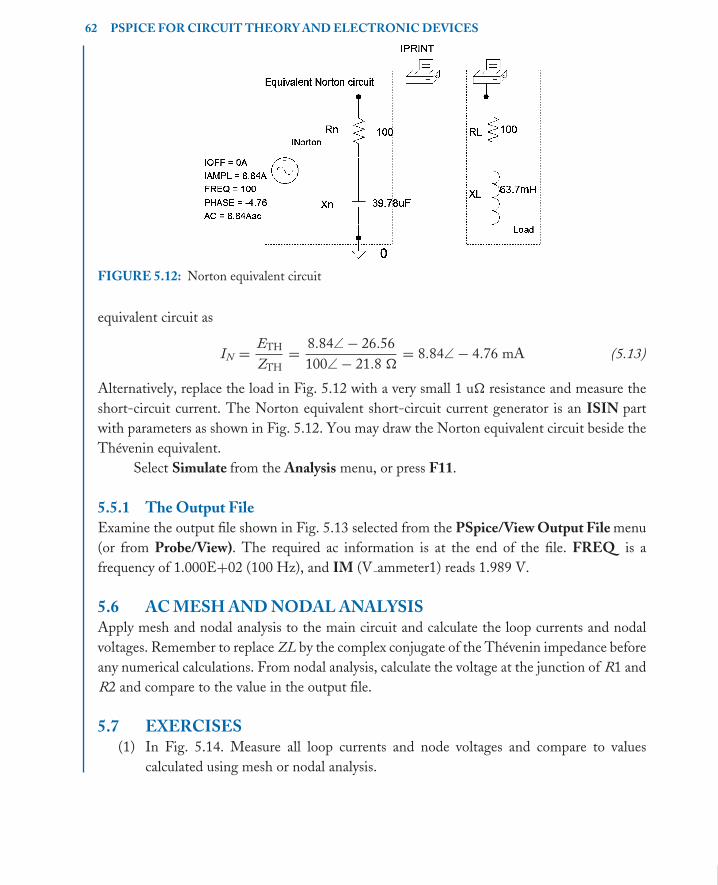
book Mobk059 March 9, 2007 10:21
62 PSPICE FOR CIRCUIT THEORY AND ELECTRONIC DEVICES
FIGURE 5.12: Norton equivalent circuit
equivalent circuit as
IN =ETH
ZTH=
8.84∠ − 26.56
100∠ − 21.8 �= 8.84∠ − 4.76 mA (5.13)
Alternatively, replace the load in Fig. 5.12 with a very small 1 u� resistance and measure the
short-circuit current. The Norton equivalent short-circuit current generator is an ISIN part
with parameters as shown in Fig. 5.12. You may draw the Norton equivalent circuit beside the
Thevenin equivalent.
Select Simulate from the Analysis menu, or press F11.
5.5.1 The Output FileExamine the output file shown in Fig. 5.13 selected from the PSpice/View Output File menu
(or from Probe/View). The required ac information is at the end of the file. FREQ is a
frequency of 1.000E+02 (100 Hz), and IM (V ammeter1) reads 1.989 V.
5.6 AC MESH AND NODAL ANALYSISApply mesh and nodal analysis to the main circuit and calculate the loop currents and nodal
voltages. Remember to replace ZL by the complex conjugate of the Thevenin impedance before
any numerical calculations. From nodal analysis, calculate the voltage at the junction of R1 and
R2 and compare to the value in the output file.
5.7 EXERCISES(1) In Fig. 5.14. Measure all loop currents and node voltages and compare to values
calculated using mesh or nodal analysis.

book Mobk059 March 9, 2007 10:21
AC CIRCUITS AND CIRCUIT THEOREMS 63
FIGURE 5.13: The output file
(2) Investigate the schematic in Fig. 5.15 and measure all loop currents and node
voltages.
(3) Develop a Norton equivalent circuit with respect to the load ZL, for the circuit
shown in Fig. 5.16. Hence, calculate component for the equivalent circuit and a
value for ZL, for maximum power transfer. If the load ZL is replaced by a voltage
source V 2, apply nodal analysis and obtain an equation in matrix form relating the
circuit components and parameters. R1 = 100 �, R2 = 20 �, XL = j618 �, V1 =10 sin 2π100t V.
(4) For the network in Fig. 5.17, write expressions for the currents in XL1 andXL2 in a
matrix form. Calculate the node voltage at the junction of XL1 and XL2 using nodal
analysis. R1 = 100 �, XL1 = XL2 = j100 �, V 1 = 1 ∠0 V, V 2 = 2 ∠0 V.
FIGURE 5.14: Mesh problem

book Mobk059 March 9, 2007 10:21
64 PSPICE FOR CIRCUIT THEORY AND ELECTRONIC DEVICES
FIGURE 5.15: Mesh problem
FIGURE 5.16: Mesh problem
FIGURE 5.17: Mesh problem: Series and parallel resonant circuits

book Mobk059 March 9, 2007 10:21
65
C H A P T E R 6
Series and Parallel-tuned Resonance
6.1 RESONANCEThe resonance phenomenon occurs in a second-order system containing capacitors and induc-
tors. A circuit containing resistance, capacitance, and inductance will become purely resistive
at the resonant frequency when the inductive reactance equals the equal capacitive reactance.
Selectivity is the ability of the resonant circuit to extract the resonant frequency and attenuate
other frequencies. Selectivity is measured by a Q-factor, which, for a series-tuned circuit, is
the ratio of the inductive (or capacitive reactance) to the total resistance in the circuit (this
includes source and load resistances). It is a measure of how well the circuit extracts a band of
frequencies with little attenuation but rejects other frequencies outside this band. Selectivity is
also dependent on the inductor-capacitor ratio.
A high Q-factor value means high selectivity and a low Q-factor means low selectivity.
For good series-tuned selectivity, the circuit must be fed from a voltage source because the
source resistance feeding the circuit has minimum resistance and hence has minimum effect on
the Q-factor (Ideal voltage source impedance is zero). Any series resistance added will reduce
the overall selectivity. A parallel-tuned circuit is fed from a current source because it has a high
source resistance and hence minimum loading. Any external resistive loading reduces the overall
selectivity of the parallel-tuned circuit.
6.2 SERIES-TUNED CIRCUITFig. 6.1 shows a series-tuned circuit with inductance, capacitance, and resistance R representing
source and coil resistances. The total circuit impedance is
Z = ES/ lS = R + j (XL − XC ) (6.1)
The total reactance is zero at the resonant frequency f 0 ( j terms are zero).
(XL − XC ) = 0 ⇒ XL = XC or ωL = 1/ωC (6.2)

book Mobk059 March 9, 2007 10:21
66 PSPICE FOR CIRCUIT THEORY AND ELECTRONIC DEVICES
FIGURE 6.1: A series-tuned circuit
Cross-multiplying (6.2) yields an expression for resonance as
ω2 =1
LC⇒ ω =
1√
LC⇒ f0 =
1
2π√
LC(6.3)
Below resonance, the circuit impedance is capacitive i.e. a leading phase angle. Above resonance
the circuit is inductive i.e. lagging phase angle and at f0, the phase is zero ( j term is zero).
6.2.1 Current ResponseMaximum current flows at resonance when the circuit is purely resistive. We can measure the
−3 dB bandwidth from the current response in Fig. 6.2 by expanding the area around the
−3 dB area using the magnifying glass icon. However, it may be necessary to simulate again
but with a smaller frequency range for better resolution.
FIGURE 6.2: Current response

book Mobk059 March 9, 2007 10:21
SERIES AND PARALLEL-TUNED RESONANCE 67
6.3 EXAMPLEA VSIN generator ES = 10 sin 2π f tV is connected to a series-tuned circuit. L = 470 uH and
C = 10 nF. If the total resistance is 4 �, calculate and verify by simulation: The frequency of
resonance f0, the phase of the circuit a decade above and below f0, and the value of the current
at f 0.
6.3.1 SolutionResonance occurs at f0 = 1/2π
√LC = 73 · 45. The phase is θ = tan−1(XL − XC )/R =
tan−1(2π f L − 1/2π f C)/R. The phase a decade above resonance f = 734.5 kHz is θ =tan−1(2167 · 9 − 21 · 679)/4 = 89◦53′. The phase a decade below resonance f = 7.345 kHz
is θ = tan−1(21.679 − 02167.9)/4 = −89◦53. The impedance at resonance is
Z = R + j (XL − XC ) = 4 + j (216 · 79 − 216 · 79) = 4 + j0 �
The current at resonance is calculated by dividing the voltage by the impedance:
is ( f0) = ES/R = 10 sin 2π f t/4 = 2 · 5 sin 2π f t
6.4 Q-FACTORThe Q-factor is a measure of SELECTIVITY which is the ability of a resonant circuit to select
out a band of frequencies whilst attenuating other frequencies outside this band. The Q-factor
is obtained from the ratio of the energy stored in the coil reactance to the energy dissipated in
the circuit resistance. Typical coil Q-factors’ range is 20–80, but capacitor Q-factors are much
bigger with values in the thousands. Because of the large difference in Q-factor values, the
resonant circuit selectivity is determined mainly by the inductor Q-factor.
Q =Energy stored
Energy dissipated per cycle=
ωL
R=
reactance
resistance=
1/ωC
R=
1
ωC R(6.4)
6.4.1 The −3 dB BandwidthTo compare the selectivity of resonant circuits, we introduce the −3 dB bandwidth defined
as the difference in two frequencies, f 1, and f 2, frequencies where the output voltage falls
by 3 dB from the maximum at f 0. At these frequencies, the resistance in the circuit is equal
to the total reactance i.e. R = XT = XL − XC = 2π fi L − 1/2π fi C . However, the total re-
actance decreases on either side of the resonant frequency, so we equate the resistance to
the reactance on either side and solve. Capacitive reactance below resonance is greater than
inductive reactance i.e. R = 1/ω1C − ω1L = ω2L − 1/ω2C so multiplying by ω1C yields
1 − ω21 LC = ω1ω2LC − ω1C/ω2C . At resonance, this reduces toLC = 1/ω2
0. To obtain an
book Mobk059 March 9, 2007 10:21
68 PSPICE FOR CIRCUIT THEORY AND ELECTRONIC DEVICES
expression for the quality factor, replace LC to yield:
1 −ω2
1
ω02
=ω1ω2
ω20
−ω1
ω2= 1 +
ω1
ω2=
ω1ω2
ω20
+ω2
1
ω20
(6.5)
ω1 + ω2
ω2=
ω1(ω1 + ω2)
ω20
= ω20 = ω1ω2 (6.6)
f 20 = f1 f2 ⇒ f0 =
√
( f1 f2) (6.7)
The relationship between f 0, BW, and Q is
Q = f0/BW (6.8)
Any resistance added to a series-tuned circuit decreases the Q-factor, so the circuit must be
fed from a voltage source and not a current source. However, a real voltage source has resistance
and will reduce the overall selectivity.
6.5 VOLTAGES ACROSS L AND C AT RESONANCEWe will now see how we can get voltage magnification in passive resonant circuits—a phe-
nomenon called Q-magnification. The current at the resonant frequency, f0, is
i = ES/R (6.9)
Hence, the inductor voltage is
VL = i j XL (6.10)
Substituting (6.9) into (6.10) yields the magnitude of the inductor voltage as
|VL| = ES(XL)/R (6.11)
Since the quality factor is Q = XL/R, then
|VL| = QES (6.12)
The voltage across the inductor is Q times the source voltage at resonance (Nikola Tesla
1856–1943). A similar analysis for the capacitor voltage Vc = −i j XC yields
|Vc | = ES XC/R = QES (6.13)

book Mobk059 March 9, 2007 10:21
SERIES AND PARALLEL-TUNED RESONANCE 69
FIGURE 6.3: Voltage response across R = 200 �, C , and L
The capacitor voltage is Q times the applied voltage and occurs across L and C at resonance
forming the basis of the Q-meter. For example, if ES = 10 V and Q = 50, then the voltage
VL across the coil is 500 V. Q-magnification results in peak voltages as shown in Fig. 6.3 for
R = 20 �, C = 10 nF, and L = 470 uH. The peaks will tend to merge at the resonant frequency
for Q-factors greater than 10, but will separate for low value Q-factors.
The voltage across the inductance falls off at low frequencies displaying high-pass filter
characteristics, whilst the voltage across the capacitor rolls-off at high frequencies giving a
low-pass filter response. The resistor voltage, on the other hand, has a bandpass response.
The voltages across C and L are picked up using differential voltage markers from the
Marker menu. The peak separation is evident only for low Q-factor values (this is achieved
by increasing the resistance to 200 �). Note: An alternative to plotting the resistor voltage
is to including the node at either end of the resistor in the trace expression dialogue box
in the Probe screen as V (R1:2) -V (R1:1). These are the alias voltages at either end of the
resistance.
To obtain an expression for the frequency at which the peak capacitor voltage occurs
means differentiating the capacitor voltage with respect to frequency and equating the result to
zero. Another useful facility in probe is the Append command found in the File menu where
you may combine simulation data from another simulation e.g. example.dat. However, the
appended file must have a different name, and have the same x-axis settings. Measure the peak
voltages V C and V L. The maximum voltage is Q times the source voltage, so we may calculate
a value by dividing the maximum voltage by the source voltage. To change the cursor from one
trace to another, click the diamond/square symbol at the bottom of the Probe output besides
the measured parameter.

book Mobk059 March 9, 2007 10:21
70 PSPICE FOR CIRCUIT THEORY AND ELECTRONIC DEVICES
6.6 UNIVERSAL RESPONSE CURVEThe normalized current in a series-tuned circuit is defined by a universal response curve equation
that contains two factors: a fractional de-tuning factor x and the Q-factor and is defined as
i =ES
Z=
ES
R + j (XL − XC )=
ES/R
1 + j (XL − XC )/R(6.14)
At f 0, maximum current is i0 = Es /R, so substitute into (6.14)
i =i0
1 + j (ωL − 1/ωC)/R(6.15)
Take out ωL
i =i0
1 + j ωLR (1 − 1
ω2 LC)
=i0
1 + j (ω0
ω0)ωL
R (1 − 1ω2 LC
)=
i0
1 + j (ω0 LR ) ω
ω0(1 − 1
ω2 LC)
(6.16)
where ω20 = 1/LC and Q0 = ω0L/R.
i =i0
1 + j Q0 (ω/ω0 − ω0/ω)(6.17)
Normalize the current by dividing by i0 to give the magnitude and angle as
∣
∣
∣
∣
i
i0
∣
∣
∣
∣
=1
√
1 + Q20 (ω/ω0 − ω0/ω)2
∠ − tan−1 Q0 (ω/ω0 − ω0/ω) (6.18)
6.7 SELECTIVITY OF A SERIES-TUNED RESONANT CIRCUITWe use a Param part from the special.olb library to investigate how resistance changes the
circuit bandwidth as shown in Fig. 6.4. Select the PARAM part, Rclick, and select Edit
FIGURE 6.4: Selectivity testing

book Mobk059 March 9, 2007 10:21
SERIES AND PARALLEL-TUNED RESONANCE 71
FIGURE 6.5: Selectivity versus circuit resistance
Properties. Enter a new row in the spreadsheet and place Rvar in the first column and 1 in the
second column.
DLclick the R1 value and enter {Rvar} (Make sure to include the brackets {}). From the
Analysis Setup menu, click Parametric, and set the following parameters: Global Parameter,
Sweep Type = Linear, Name = Rvar, Start Value = 1, End Value = 200, Increment = 50.
Enter Rvar (no curly brackets) in the name box, and set the Start, End, and Increment to: 50,
200, and 50. Click on AC Sweep and set the Analysis tab to Analysis type: AC Sweep/Noise,
AC Sweep Type to Linear, Start Frequency = 50k, End Frequency = 150k, Points/Decade
= 1000 to produce the response shown in Fig. 6.5.
Measure the −3 dB bandwidth for the biggest resistance and calculate the Q-factor
value. Compare to the measured value. The resistance determines the selectivity because the
larger the resistance, the larger the bandwidth but a smaller Q-factor results. The bandwidth is
1 kHz for a resonant frequency f0 = 100 kHz, and the loaded Q-factor is 100 (remember
BW = f0/QL). Set the Start Frequency = 10k, End Frequency = 1000k and Points/Decade
= 1000. For detailed information around the resonant frequency region, choose a Linear sweep
in the set-up menu and reduce the frequency range between 90 kHz and 110 kHz and simulate.
Reducing the frequency axis in Probe will not increase the resolution.

book Mobk059 March 9, 2007 10:21
72 PSPICE FOR CIRCUIT THEORY AND ELECTRONIC DEVICES
FIGURE 6.6: Phase marker
6.7.1 L/C Ratio and SelectivityThe Q-factor changes when the L/C ratio in a series-tuned circuit is changed. Since Q = ω0L/r
and ω0 = 1/√
LC , then substituting for the resonant frequency yields
Q =1
√LC
L
r=
1
r
√
L
C(6.19)
The Q-factor is proportional to the L/C ratio and is inversely proportional to the circuit
resistance. In Fig. 6.6, calculate the resonant frequency f0, Q-factor, and the −3 dB band-
width for R = 2� and 200 �, and verify these values from the current amplitude (IR) and
phase responses (Ip) for R = 2�. Measure the resonant frequency and the −3 dB band-
width. Repeat for R = 200 �, and plot VL, VC , VR, and the circuit impedance “seen” by the
source.
6.8 SERIES-TUNED LC R PHASE RESPONSEFig. 6.6 shows a current phase marker placed across the 20 � resistor to plot the phase
response.
Be very careful about placing and rotating components on the screen, as it may produce
unexpected results. With the cursor icon selected, pressing the icon makes the cursor jump
to the middle of the phase response. Pressing the icon places x and y signal values at this
point. For very high Q values, the slope of the phase response is very steep around resonance, so
you might not be able to measure accurately the phase at resonance. One solution is to increase
the number of points plotted and/or decrease the frequency range around resonance. Press F11
to obtain the phase response in Fig. 6.7.
Select the magnifying glass icon to examine the region around the resonant point. If the
response is not smooth, repeat the analysis but with a reduced frequency range and an increased
number of points. Measure the frequency on the phase response at −45◦, 0◦, and +45◦ and
calculate the bandwidth. Lclick the mouse button for the first cursor and move the mouse,

book Mobk059 March 9, 2007 10:21
SERIES AND PARALLEL-TUNED RESONANCE 73
FIGURE 6.7: Current phase response
then click the right mouse button for the second cursor. The cursors may be moved to find the
−3 dB frequency values (If the display is not in dB, then measure the frequency where the
voltage is reduced by 70.7% of the maximum voltage). For example, if the maximum voltage is
10 V, then measure the frequencies f1 and f2 on either side of the resonant frequency where
the voltage is reduced to 7.07 V. Dividing f 0 by the BW to calculate the loaded Q-factor.
From the phase response, compare measured and calculated bandwidths.
6.9 IMPEDANCE OF A SERIES-TUNED CIRCUITTo plot the circuit impedance, run a simulation without markers placed on the circuit. From
the Probe screen, click the Trace menu (or press the insert key), and add a trace as in Fig. 6.8.
From the list, select V(VIN) and insert “/” in the Trace Expression box at the bottom left side
of the screen end and then select I(Vin).
The impedance of the tuned circuit Z = V(source)/ I(Vin) is plotted in Fig. 6.9 with the
x-axis set to log. A minimum value occurs at the resonant frequency and is the resistance of the
inductor.
FIGURE 6.8: Trace expression box

book Mobk059 March 9, 2007 10:21
74 PSPICE FOR CIRCUIT THEORY AND ELECTRONIC DEVICES
FIGURE 6.9: Series impedance plot
6.10 FOURIER SERIESA periodic function, f (t), with period T and fundamental frequency, f 0, may be generated
using the sum of N weighted cosine and sine components using the Fourier series expansion
(Joseph Fourier 1768–1830):
f (t) = V0 +N
∑
n=1
(an cos 2πn f0t + bn sin 2πn f0t) (6.20)
V 0 is a DC term, f 0 is the fundamental frequency of the signal and weighting coefficients an
and bn. Thus, a square wave may be broken into a series of harmonic terms and represented by
the equation in (6.20) [ref: 6].
6.10.1 Series-Tuned Circuit as a Low-Pass FilterA 100 kHz square wave applied to the series-tuned resonant circuit in Fig. 6.10 has the
fundamental component of the 100 kHz square wave extracted by the low-pass filter.
FIGURE 6.10: Second-order LPF

book Mobk059 March 9, 2007 10:21
SERIES AND PARALLEL-TUNED RESONANCE 75
TABLE 6.1: VPULSE Parameters
DC = 0 (offset)
AC = 0.1 (amplitude)
V1 = 0 (space value)
V2 = 1 (mark value)
TD = 0 s (delay time)
TR = 0.1 us (rise time)
TF = 0.1 us (fall time)
PW = 5 us (pulse width)
PER = 10 us (pulse period)
Place a VPULSE generator from the source.olb library and set the parameters as shown
in Table 6.1. Enter numerical values only (The parameter description is for your informa-
tion only). The pulse period PER Tp = 10 us is the inverse of the resonant frequency
f0 = 100 kHz and the pulse width PW = 5 us (for an equal mark-space ratio).
6.10.2 The Output FileThe junction at L and C is labeled out. Select the analysis set-up icon and set the parameters
as shown. Select the Output File Options as shown in Fig. 6.11, and tick the Perform
Fourier Analysis parameters. The two variable entered in Output Vars box are: V(in) V(out),
where in and out are the wire segment names separated by a space. The input and output
spectral information will be in the output file accessed from the PSpice/View Output File
menu.
FIGURE 6.11: Transient set-up

book Mobk059 March 9, 2007 10:21
76 PSPICE FOR CIRCUIT THEORY AND ELECTRONIC DEVICES
FIGURE 6.12: Input and output signals
Press F11 to simulate. The plot shown in Fig. 6.12 is for R = 20 �.
The extra plots were obtained pressing Alt PP keys and copying the input and output
variables onto the extra plots. From Probe, select Plot/Unsynchronize X Axis menu to change
the horizontal axis to frequency. Press the FFT icon to display the two plots in the frequency
domain. The extracted 100 kHz sine wave signal has a period of 10 us. The step size is
automatically adjusted by the PSpice dynamic internal algorithm step size change, increasing
its size during periods when there is little activity, but decreasing the step size for rapid time
changing events. Too large a Maximum step size value makes the display too course and
angular in shape. The ratio Run to time/Maximum step size specifies the number of points
plotted. For example, 100 points are plotted if the ratio is 100 us/1 us. A small Maximum
step size value will make the analysis time longer but it will produce a smoother-looking plot
(reduce this parameter if you have convergence problems). If you observe triangular-shaped
signal waveforms, as in Fig. 6.13, it means the maximum step size chosen is not small enough.
A rule of thumb is to set the Maximum step size to Run to time /1000. So for example, if Run
to time = 15 s, then Maximum step size is set to 15 ms.
The Start saving data after is useful if you wish to calculate and display data from a
time other than zero. For example, set the delay to 99 us if you wish to plot the signal starting
from 99 us. It is also useful for reducing the output data contained in the Probe output file (file
extension .out). Repeat the above simulation for R = 200 �.
6.11 SKIP INITIAL CONDITIONSIn the Analysis Setup/Transient menu, the Skip initial conditions forces PSpice to use initial
conditions on an inductor or capacitor. If not checked, PSpice calculates the initial conditions

book Mobk059 March 9, 2007 10:21
SERIES AND PARALLEL-TUNED RESONANCE 77
FIGURE 6.13: Maximum step size too large results in a distorted plot
treating capacitors as open circuits and inductors as short circuits. Care must be taken to
ensure that the Skip initial conditions box is unchecked in schematics where initial conditions
are required. The Fast Fourier Transform icon (FFT) in Probe is useful for examining the
frequency components of a complex signal, as demonstrated in Fig. 6.14.
Increase the Run to time and/or decrease the Maximum step size to increase the FFT
resolution. The spectrum of the output signal displayed in the top plot shows higher spectral
components almost eliminated by the filtering action of the circuit.
6.12 PARALLEL-TUNED LC R CIRCUITThe parallel-tuned circuit in Fig. 6.15 shows a capacitor in parallel with an inductor whose
series coil resistance is r c . The circuit is fed from a current source comprising an ideal current
source in parallel with a large source resistance value, hence the source resistance will produce
FIGURE 6.14: Spectrum of a square wave

book Mobk059 March 9, 2007 10:21
78 PSPICE FOR CIRCUIT THEORY AND ELECTRONIC DEVICES
FIGURE 6.15: Parallel LCR circuit
minimum loading. Note: In PSpice, the voltage and current sources are ideal, hence a current
source resistance is an open circuit, whilst a voltage source resistance is a short circuit. We
need to add a resistance across the current source in order to simulate, otherwise an error will
occur. Likewise, it is good practice to add a source resistance in series with a voltage source.
Sometimes it is necessary to represent a current source as a voltage source in series with a high
resistance.
It is easier to analyze this circuit if we replace the coil resistance and reactance of the series
branching Z = Rc + jωL with an equivalent parallel admittance consisting of a conductance G
and susceptance B, i.e. Y = G + j B.
Y =1
Z=
1
Rc + jωL×
Rc − jωL
Rc − jωL=
Rc
R2c + ω2L2
− jωL
R2c + ω2L2
= G + j B (6.21)
Inverting the conductance G gives the equivalent parallel resistance
RP =1
G=
R2c + ω2L2
Rc= Rc +
ω2L2
Rc= Rc +
ω2L2
Rc
(
×Rc
×Rc
)
= Rc +ω2L2
R2c
Rc (6.22)
Introduce the Q-factor Q0 = ωLRc
into (6.22)
RP = Rc + Q20 Rc (6.23)
This resistance is called the dynamic impedance of the circuit at resonance (it is resistive at
resonance). We can make the approximation RP ≈ Q20 Rc , and is valid for Q0 > 10. The parallel
reactance is
XLP =1
B=
R2c + ω2L2
ωL= ωL +
R2c
ωL
(
×ωL
×ωL
)
= ωL +(
Rc
ωL
)2
ωL (6.24)

book Mobk059 March 9, 2007 10:21
SERIES AND PARALLEL-TUNED RESONANCE 79
FIGURE 6.16: Equivalent parallel LCR circuit
Substituting for the unloaded Q-factor yields
XLP = ωL +ωL
Q2(6.25)
The circuit is now represented by the equivalent circuit shown in Fig. 6.16.
For Q values greater than 10, we make the approximation that the parallel inductive
reactance is equal to the series inductive reactance i.e. XLP ≈ XLS = ωL. At resonance, the
total reactance is zero, so XLP = XLS = XC .
R2c + ω2
0 L2
ω0L=
1
ω0C⇒ R2
c + ω20 L2 = L/C (6.26)
Rearranging (6.26) gives an expression for the frequency of resonance as
ω20 =
1
L2
[
L
C− R2
c
]
=1
LC−
R2c
L2(6.27)
Expressed in hertz:
f0 =1
2π
√
1
LC−
R2c
L2(6.28)
From (6.22) we can write
G =Rc
R2c + ω2L2
=1
RP(6.29)
Replacing R2c + ω2L2 with L/C from (6.26) yields the dynamic impedance as
RP =L
Rc C(6.30)

book Mobk059 March 9, 2007 10:21
80 PSPICE FOR CIRCUIT THEORY AND ELECTRONIC DEVICES
To express Q in terms of the dynamic impedance Rp and XL, multiply (6.30) by the resonant
frequency as
RP =L
C Rc
(
ω0
ω0
)
=ω0L
ω0C Rc(6.31)
The Q-factor is Q0 = ω0 LRc
= 1ω0C Rc
, so we may write (6.31) as
RP = ω0LQ0 = Q0/ω0C (6.32)
6.12.1 Universal Response CurveThe normalized impedance of a parallel-tuned circuit is expressed in terms of the Q-factor and
the fractional de-tuning factor, x. The impedance of a parallel-tuned circuit is
Z =(Rc + j XL)(− j XC )
Rc + j XL − j XC(6.33)
We simplify this expression by assuming a high Q-factor coil, so that XL ≫ rc
Z =XC XL
Rc + j (XL − XC )=
L/C
Rc + j (XL − XC )(6.34)
Dividing (6.34) above and below by r c
Z =L/C Rc
1 + j1/Rc (XL − XC )(6.35)
The impedance at resonance is called the dynamic impedance RP = L/C Rc , even though it is
resistive. Divide (6.35) by the dynamic impedance to normalize as
Z
RP=
1
1 + j1/Rc (XL − XC )=
1
1 + jωL/Rc (1 − 1/ω2LC)=
1
1 + jωL/Rc (1 − ω20/ω
2)(6.36)
Z
RP=
1
1 + j ωLRc
× ω0
ω0(1 − ω2
0
ω2 )=
1
1 + j ωLRc
× ω0 LRc
( ωω0
− ω0
ω)
=1
1 + j Q0
(
ωω0
− ω0
ω
) (6.37)
The fractional de-tuning factor, x, is
x =ω0 − ω
ω0= 1 −
ω
ω0⇒
ω
ω0= 1 − x (6.38)
So that ωω0
= 1 − x ⇒ ω0
ω= 1
1−x . Combine these two equations yields
ω
ω0−
ω0
ω=
1 − x
1−
1
1 − x=
1 − 2x + x2 − 1
1 − x=
x2 − 2x
1 − x(6.39)

book Mobk059 March 9, 2007 10:21
SERIES AND PARALLEL-TUNED RESONANCE 81
Substitute (6.39) into (6.37) and express the magnitude of the result as∣
∣
∣
∣
Z
RP
∣
∣
∣
∣
=1
√
1 + Q20
(
ωω0
− ω0
ω
)2=
1√
1 + Q20
(
x2−2x1−x
)2(6.40)
For x ≪ 1, i.e. frequencies close to f 0 we can approximate (6.40) as∣
∣
∣
∣
Z
RP
∣
∣
∣
∣
≈1
√
1 + 4Q20x2
(6.41)
Expressed in terms of the fractional de-tuning, α∣
∣
∣
∣
Z
RP
∣
∣
∣
∣
=1
√
(1 + 4Q20α
2(6.42)
6.12.2 Relationship Between the Resonant Frequency and Bandwidth
A similar result for the series-tuned normalized current is |i/ i0| = 1/
√
1 + 4Q20α
2, hence the
normalized power is
i2 R
i20 R
=P
P0=
1
1 + 4Q20x2
(6.43)
The −3 dB frequency is where the maximum output power P 0 falls to half of its value.
1 + 4Q20x2 = 2 ⇒ 4Q2
0x2 = 1
4Q20x2 = 1 ⇒ x2 =
1
4Q20
⇒ x = ±1
2Q0
Defining x as
x =ω0 − ω
ω0=
1ω
ω0=
1 f
f0= ±
1
2Q0(6.44)
Since the bandwidth is 21 f , we may write
21 f
f0=
BW
f0=
1
Q0⇒ Q0 =
f0
BW(6.45)
6.12.3 Loaded Q-factorA parallel-tuned circuit is connected to a nonideal current source with a high impedance
source. The source will load the tuned circuit because any extra resistance in parallel reduces
the Q-factor. Because of this, we must introduce the loaded Q-factor. The equivalent parallel

book Mobk059 March 9, 2007 10:21
82 PSPICE FOR CIRCUIT THEORY AND ELECTRONIC DEVICES
resistance at resonance is the dynamic impedance Rp and is reduced by any external resistance
REXT placed in parallel with the circuit. The loaded Q-factor is QL = RT/XL, with the total
resistive loading RT = RS//RP//REXT = RRP
R+RP= RP
1+RP /R , and R = RS REXT/(RS + REXT).
6.13 EXAMPLEThe drain circuit of a FET tuned radio frequency amplifier has a 100 pF capacitor placed in
parallel with an inductor L, whose unloaded Q-factor is 100. If the frequency of resonance is
1 MHz and the transistor output resistance is 20 k�, calculate the loaded Q-factor, inductance,
and loaded bandwidth.
6.13.1 SolutionThe total resistive loading on the tuned circuit consists of the transistor output impedance and
the dynamic impedance in parallel R = RS RP/(RS + RP ). The dynamic impedance using the
unloaded Q-factor is
RP =QU L
ω0C=
100
2π (1 × 10⁶)(100 × 10−12)=
106
2π� = 159 k�
Substitute the two impedances, gives the total resistive loading R = 20.103×159.103
20.103+159.103 = 17.76 k�.
Since the unloaded Q-factor is greater than 10, then the dynamic impedance RP ≈Q2
U L Rc , hence the coil resistance is 159 × 103/(100)2 = Rc = 15.9 �. The loaded Q-
factor QL = QU I
1+RP /R = 1001+159k/17.76k = 10 and the unloaded Q-factor is QU L = ω0L/Rc ⇒
L = QU L Rc /ω0 = 100(15 · 9)/2π (1 × 10⁶) = 0 · 253 mH. The unloaded bandwidth is
f 0/QU L = 1 MHz/100 = 10 kHz, and the loaded bandwidth is 1 MHz/10 k = 100 kHz
[ref: 3].
6.14 PROBLEMFor the circuit in Fig. 6.17, calculate the unloaded and loaded Q-factors, resonant frequency,
the −3 dB bandwidth (BW) and the dynamic impedance. Compare these calculations to
the simulate resultants from the voltage amplitude response. Plot the phase and impedance
responses across the circuit (do not include the source resistance).
An ideal voltage source resistance is zero, so connecting it across a parallel LCR circuit
would destroy the circuit selectivity. The circuit must therefore be fed from a current source
(An ideal current source has an infinite source resistance) and here we mimic a current source
as a voltage source in series with a high source resistance. Set the Analysis tab to Analysis type:
AC Sweep/Noise, AC Sweep Type to Logarithmic, Start Frequency = 100, End Frequency
= 1000k, Points/Decade = 1000. In general, to set the frequency range you need to calculate

book Mobk059 March 9, 2007 10:21
SERIES AND PARALLEL-TUNED RESONANCE 83
FIGURE 6.17: Thevenin equivalent circuit for a current source
the resonant frequency first. The Start Frequency and End Frequency values are then set a
decade above and below the resonant frequency and the x-axis set to Linear.
6.15 FREQUENCY RESPONSE OF A PARALLEL-TUNED CIRCUITThe parallel-tuned frequency response is shown in Fig. 6.18.
Use the cursors and magnifying tool to measure the −3 dB bandwidth and resonant
frequency accurately. If the plot looks triangular, reset the frequency range from 90 k to 120 k
and simulate. Remember using the magnifying tool does not increase the number of plotted
points, so you need to reduce the frequency range and/or the number of points plotted. From
Probe/Trace/Evaluate measurement menu, press the sixth icon shown in Fig. 6.19.
FIGURE 6.18: Output voltage in dB

book Mobk059 March 9, 2007 10:21
84 PSPICE FOR CIRCUIT THEORY AND ELECTRONIC DEVICES
FIGURE 6.19: Evaluate measurement icon
Select the −3 dB bandwidth (1 dB) function Bandwidth (1, dB) function from the list
shown in Fig. 6.20. Replace “1” with the required function i.e. Bandwidth(V(Ct:2), 3), where
3 represents the −3 dB point.
From the Trace/Measurements menu the sub menu in Fig. 6.21 appears. Pressing Eval
opens a further menu and you need to browse the directory and insert the function V(Ct:2) to
display the bandwidth as 3.966 kHz. However, this information disappears when you press ok.
Place a phase marker from the PSpice/Markers/Advanced menu to observe the phase
response shown in Fig. 6.22.
The phase at the resonant frequency is zero, but why is the phase of the voltage and current
zero at DC (Hint: Assume the capacitor reactance is infinite and the inductive reactance is zero
at very low frequencies)?
6.16 DYNAMIC IMPEDANCETo plot the impedance of the circuit, press the insert button on the keyboard, and in the Trace
Expression box shown in Fig. 6.23, insert V1(Vsource)/ I(Vsource).
The circuit impedance Z = V1(Vsource)/I(Vsource) is shown in Fig. 6.24. Measure the
impedance at the resonant frequency and subtract the 50 k� source resistance and verify the
dynamic impedance is (Rp = L1/Ctrc ) = 8.7 k�.
6.16.1 Loaded and Unloaded Q-factorAny extra resistance in parallel with the tuned circuit reduces the unloaded Q-factor to a smaller
value called the loaded Q-factor, so a current source, although having a high source impedance,
FIGURE 6.20: The −3 dB BW evaluate measurement function

book Mobk059 March 9, 2007 10:21
SERIES AND PARALLEL-TUNED RESONANCE 85
FIGURE 6.21: Measurement function display
still reduces the dynamic impedance and hence the Q-factor. To determine the Q-factor, the
dynamic resistance Rp , and the AC coil resistance Rc, draw the schematic in Fig. 6.25. Set the
VSIN generator to 10 V at a resonant frequency of 100 kHz. Measure the output voltage across
the capacitor. From potential division, and the measured values input and output voltages V s
and V out, calculate the dynamic impedance Rp , the AC coil resistance Rc , and QU L.
FIGURE 6.22: Phase relationship for the capacitor voltage
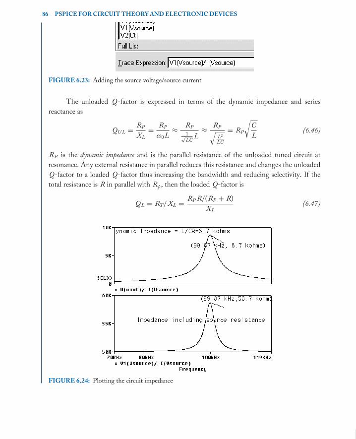
book Mobk059 March 9, 2007 10:21
86 PSPICE FOR CIRCUIT THEORY AND ELECTRONIC DEVICES
FIGURE 6.23: Adding the source voltage/source current
The unloaded Q-factor is expressed in terms of the dynamic impedance and series
reactance as
QU L =RP
XL=
RP
ω0L≈
RP
1√LC
L≈
RP√
L2
LC
= RP
√
C
L(6.46)
RP is the dynamic impedance and is the parallel resistance of the unloaded tuned circuit at
resonance. Any external resistance in parallel reduces this resistance and changes the unloaded
Q-factor to a loaded Q-factor thus increasing the bandwidth and reducing selectivity. If the
total resistance is R in parallel with Rp , then the loaded Q-factor is
QL = RT/XL =RP R/(RP + R)
XL(6.47)
FIGURE 6.24: Plotting the circuit impedance

book Mobk059 March 9, 2007 10:21
SERIES AND PARALLEL-TUNED RESONANCE 87
FIGURE 6.25: Q-factor measurement
R is the source resistance in parallel with external resistive loading REXT, hence the total
resistance is R = RS REXT/(RS + REXT). The loaded Q in terms of the unloaded Q-factor is
QL =RP
XL
1
1 + RP/R=
QU L
1 + RP/R(6.48)
The Q-factor increases as the C/L ratio increases and is the opposite result to that obtained
for the series-tuned circuit. Simulate to produce the result in Fig. 6.26. The output voltage is
calculated by potential division at f 0, as 4.39 V for an input Vin = 10 V:
Vout = VinRP
RP + Rs=
Vin
1 + Rs /RP(6.49)
Rs is the source resistance and the dynamic impedance RP = L/C Rc (Rc is the ac coil resistance
and is not easily measured but assume 10 �). If the measured voltage across the circuit is 4.39
FIGURE 6.26: Measure the voltage at f0

book Mobk059 March 9, 2007 10:21
88 PSPICE FOR CIRCUIT THEORY AND ELECTRONIC DEVICES
V, then from potential division we have 4.38 = 10/(1 + Rs /RP ) ⇒ Rs /RP = 1.28 ⇒ RP =Rs /1.28 = 50.103/1.28 = 38.9 k�.
Compare this value to the theoretical value:
RP =L
C Rc=
10−3
2.54 × 10−9.10= 39.37 k� (6.50)
The measured resonant frequency is f 0 = 99.86 kHz and the unloaded Q-factor is calculated
as
QU L = RP/XLP ≈ RP/XLS = 38,900/(2π f0L) = 38,900/(2π99.8) = 62
The loaded Q-factor = R/XLP , is approximately equal to R/XLS, where R is Rp in parallel
with Rs equal to 21.87 k�.
6.17 TRANSFORMERSWilliam Stanley (1858–1916) built an induction coil that was the precursor to the transformer.
A transformer has primary and secondary coils magnetically coupled, with each winding wound
on the same former (core) made from materials such as iron, steel but RF transformers generally
have an air core. All PSpice schematics require a ground part so we have to attach a second
ground symbol to the secondary or a very large resistance between primary and secondary as
shown in Fig. 6.27, otherwise we get a floating error as it “sees” the secondary circuit floating.
This is a useful technique whenever a floating error occurs, for example, if the output
component is a capacitor then one end is seen as floating. The transformer used here is a
K3019PL 3C8 part in the eval.olb library and the new power markers are located on the
component as shown.
FIGURE 6.27: Transformer

book Mobk059 March 9, 2007 10:21
SERIES AND PARALLEL-TUNED RESONANCE 89
FIGURE 6.28: Transformer parameters
6.17.1 Transformer ParametersOther transformers are: K502T300 3C8, K528T500 3C8, K Linear, XFRM LINEAR and
XFRM NONLINEAR. Edit the properties by Rclicking and selecting Edit Properties to
enter the parameters as shown in Fig. 6.28.
Transformer parts such as the XFRM LINEAR part require coupling and inductance
values.
6.17.2 Matching TransformerMaximum power transfer is transferred from a source to a load only when they are equal. A
transformer can “match” a load to a source and to show this we need to derive expressions
for the primary and secondary parameters in terms of the ratio of the primary and secondary
turns-ratio. To simplify the analysis, assume the power in the primary circuit is equal to the
power in the secondary circuit—a valid approximation because transformers are very efficient
and dissipate little power, hence we may write
vP iP = iSvS ⇒ vP =iP
iSvS (6.51)
Equate the primary ampere-turns to the secondary ampere-turns as
iP NP = iS NS ⇒iP
iS=
NS
NP= n ⇒ iP =
iS
n(6.52)
Substituting (6.52) into (6.51) yields
vP = nvS (6.53)
The primary impedance is the primary voltage divided by the primary current. Substituting for
the primary current and voltage from (6.52) and (6.53) yields
ZP =vP
iP=
nvS
iS/n⇒ ZP = n2 ZS (6.54)
Fig. 6.29 shows the input and output power dissipated in the source and load resistances.

book Mobk059 March 9, 2007 10:21
90 PSPICE FOR CIRCUIT THEORY AND ELECTRONIC DEVICES
FIGURE 6.29: Matching transformer for maximum power transfer
The primary circuit “see” a much higher resistance i.e. n2 times the load resistance. For
n2 = 100, the primary circuit is “looking” at 1000 � and not 10 �. Any resistance connected
to the secondary side will appear in the primary side of the transformer, as that resistance
multiplied by the square of the turns-ratio n. A multi-winding transformer may also be created
using the K Linear part that links together individual inductor coil names.
6.18 POWER SUPPLIES: RECTIFICATION AND REGULATIONThe schematic in Fig. 6.30 shows the input 220 V RMS mains voltage (311 V peak) with a
mains frequency of 50 Hz for European electricity supplies but is 110 V/60 Hz in the United
States. The 0.001 � mains source resistance is small since it is a voltage source and R5 is a
large terra-ohm (1 T�) resistance to avoid a floating error. Differential voltage markers from
the Markers menu are placed across the secondary terminals as shown. These are necessary
since the measurement reference is not with respect to the ground. Be sure to remove R5 if you
are creating a printed circuit.
FIGURE 6.30: Power supply

book Mobk059 March 9, 2007 10:21
SERIES AND PARALLEL-TUNED RESONANCE 91
FIGURE 6.31: Setting the turns-ratio for the mains transformer
The ripple voltage is calculated
Vpeak ripple =√
3Vr (RMS) =√
3(2.4IDC/C) (6.55)
The DC voltage across C is
VDC = Vsec − Vpeak ripple (6.56)
6.18.1 Power Supply WaveformsSelect the properties by Rclicking and entering the transformer parameters: coupling = 0.999,
L1 TURNS = 2000 and L2 TURNS = 65. The primary voltage peak is 311 V, and the
secondary peak is 10 V—a turns-ratio of 30:1, as shown in Fig. 6.31.
Set the transient analysis to display a few cycles after simulation as shown in Fig. 6.32.
Verify using (6.55) and (6.56) that all voltage waveforms have the correct values.
Fig. 6.33 shows a display of the RMS and instantaneous power in the load.
6.18.2 Power Supply Voltage RegulationThe ripple voltage shown in Fig. 6.34 may manifest itself in audio power amplifiers as an audible
120 Hz mains hum (remember it is a rectified sine wave so it is twice the mains frequency
supply). To eliminate ripple we need to regulate the power supply using a voltage regulator.
The 15 V regulated power supply has a larger number of secondary winding turns to increase
the secondary output voltage in order for the LM7815 regulator to work correctly. This voltage
regulator is not part of the evaluation version so we use the symbol from mylib.olb and attach
to it the LM7815c model downloaded from the Internet.
The regulated voltage is clearly seen from Fig. 6.35 where the ripple voltage is reduced.
6.19 GROUND BOUNCEThe schematic in Fig. 6.36 investigates “ground bounce”. PSpice hides digital IC power supply
pins but we may connect power supplies to the hidden pins by DLclicking the IC and ticking
Power Pins Visible.

book Mobk059 March 9, 2007 10:21
92 PSPICE FOR CIRCUIT THEORY AND ELECTRONIC DEVICES
FIGURE 6.32: Power supply waveforms
Decouple each IC by placing a 100 nF capacitor close to the IC supply pin. In digital
circuits, fast rise-time signals produce problems in the DC supply lines because PCB power
supply tracks and IC pins possess inductance and hence, together with track capacitance,
produces oscillatory signals on the DC rails. Select the 7474 IC D flip-flop part, RClick/Edit
FIGURE 6.33: Output power

book Mobk059 March 9, 2007 10:21
SERIES AND PARALLEL-TUNED RESONANCE 93
FIGURE 6.34: Voltage regulation
Properties, to show the properties spreadsheet. In the spreadsheet tick Power Pins Visible as
shown in Fig. 6.37.
The power supply connections, normally hidden, have inductance and capacitance added
to mimic the effects of PCB and IC output capacitance and inductance and allow us to
investigate how these components produce oscillatory signals on the power supply line rails.
Observe ground bounce at the bottom of Fig. 6.38.
FIGURE 6.35: Regulated output voltage

book Mobk059 March 9, 2007 10:21
94 PSPICE FOR CIRCUIT THEORY AND ELECTRONIC DEVICES
FIGURE 6.36: Ground bounce
6.20 POWER FACTOR CORRECTIONThe circuit in Fig. 6.39 is used to investigate power factor (PF) correction as demanded by the
electricity suppliers. We use the Trace Expression facility in Probe to plot certain mathematical
expressions for the power in the circuit. The instantaneous power in a passive load is the product
of the instantaneous load current and load voltage. For a sinusoidal signal, the power is
p(t) = v(t)i(t) = Vm cos(ωt + φ)Im cos(ωt + θ ) (6.57)
FIGURE 6.37: The 7474 spreadsheet

book Mobk059 March 9, 2007 10:21
SERIES AND PARALLEL-TUNED RESONANCE 95
FIGURE 6.38: Ground bounce waveforms
Expanding (6.57) yields
p(t) = 0.5Vm Im cos θ + 0.5Vm Im cos(2ωt + φ + θ ) (6.58)
The first part of (6.57) is the average power consumed and charged for, by the electricity
suppliers. Power factor angle is zero for resistive loads and the average power is 0.5 V m I m =V RMS I RMS W. A lagging PF = cos ϕ = φ − θ is positive for inductive loads, and a negative
leading PF for capacitive loads, as shown in Fig. 6.40. To plot degrees in PSpice, we must
multiply the angle in radians by pi/180 (= 1/57.3), i.e.
V(vin : +)∗I(R1)∗cos(VP(vin : +)∗pi/180 − IP(R1)∗pi/180)
FIGURE 6.39: Power factor correction

book Mobk059 March 9, 2007 10:21
96 PSPICE FOR CIRCUIT THEORY AND ELECTRONIC DEVICES
FIGURE 6.40: Power factor waveforms
6.20.1 Average Power and Apparent PowerAs the power factor angle increases, the average power decreases, but the peak load current
remains unchanged producing increased resistive losses which increases the costs to the electrical
suppliers. They, in turn, charge the consumer for producing nonunity power factors. The
apparent power is defined as
0.5Vm Im =p(t)
cos θ=
p(t)
PFVA (6.59)
Fig. 6.40 shows the power factor varying from zero, for a pure reactive load, to unity for a
resistive load. The second term in (6.57) has a zero average value and is the power stored in
the reactive elements of the load and returned to the source. When positive, the total power is
greater than the average power and is absorbed by the load. When negative, the total power is
less than the average power. When power factors are less than 0.5, the peak value of the second
FIGURE 6.41: Parallel-tuned LCR circuit

book Mobk059 March 9, 2007 10:21
SERIES AND PARALLEL-TUNED RESONANCE 97
FIGURE 6.42: Frequency response
term exceeds the average power, and on negative peaks, power flows from the load back to the
source. Reactive power is measured in volt-amp reactive (VARS) and is Q = 0.5Vm Im sin θ .
Complex power, S, has dimensions of volt-amp (VA) and is related to average power P and
the peak reactive power, Q, as S = P + j Q, where P and Q are the resistive and reactive load
components defined: P = 0.5I 2m R and Q = 0.5I 2
m X.
6.21 EXERCISES(1) Fig. 6.41 shows a resonant circuit fed from a voltage source in series with a large
resistance Rs thus simulating a current source. Determine the −3 dB bandwidth,
loaded and unloaded Q-factor, and the dynamic impedance Rs = 110 k�, Rc = 10 �,
Ct = 5.3 nF, L1 = 470 uH,
(2) The parallel-tuned frequency response is shown in Fig. 6.42.
(3) For the LCR circuit in Fig. 6.43, with V1(t) = 5 sin 2π f t, R1 = 50 �, C1 = 10 uF,
L1 = 100 mH, determine the resonant frequency, loaded Q-factor, and maximum peak
current. Use a PARAM part/Parametric Sweep to vary the capacitance to investigate
the effect on the resonant frequency and the Q-factor (Q = 1/r√
L/C).
FIGURE 6.43: Series-tuned LCR circuit

book Mobk059 March 9, 2007 10:21
98 PSPICE FOR CIRCUIT THEORY AND ELECTRONIC DEVICES
FIGURE 6.44: Bandstop series-tuned circuit
(4) The bandstop series-tuned circuit in Fig. 6.44 has a transfer function given as
H(s ) =s L + 1/s C
R + s L + 1/s C=
s 2LC + 1
s C R + s 2LC + 1=
s 2 + 1/LC
s 2 + s R/L + 1/LC
=s 2 + ω2
0
s 2 + (ω0/Q)s + ω20
(6.60)
A bandpass transfer function is
H(s ) =R
R + s L + 1/s C=
s C R
s C R + s 2LC + 1=
s R/L
s 2 + s R/L + 1/LC
=s (ω0/Q)
s 2 + (ω0/Q)s + ω20
(6.61)
The bandstop filter response as shown in Fig. 6.45.
FIGURE 6.45: Bandstop frequency response

book Mobk059 March 9, 2007 10:21
SERIES AND PARALLEL-TUNED RESONANCE 99
FIGURE 6.46: Rectification
Show that (6.61) is the same as subtracting (6.61) from 1.
(5) In power factor correction, verify the relationship between apparent power (VA), real
power (Watts), and reactive power (VARS) as VA =√
P 2 + Q2.
(6) Investigate the power supply in Fig. 6.46.
(7) Investigate the center-tap transformer in Fig. 6.47 using XFRM LINEAR parts.
(8) Reduce the circuit in Fig. 6.48 to an equivalent series circuit, by converting the
parallel combination of C1 and R2. Hence, show that the resonant frequency is
ω0 =√
( 1C1L1 − 1
C12 R22 ). Calculate the resonant frequency, Q-factor, and the −3 dB
Bandwidth for R1 = 10 �, R2 = 100 k�, L1 = 1 mH, C1 = 1nF. Simulate and
compare measured results to the calculated values.
FIGURE 6.47: Centre-tap transformer

book Mobk059 March 9, 2007 10:21
100 PSPICE FOR CIRCUIT THEORY AND ELECTRONIC DEVICES
FIGURE 6.48: Series-tuned circuit

book Mobk059 March 9, 2007 10:21
101
C H A P T E R 7
Semiconductor Devicesand Characteristics
7.1 SEMICONDUCTOR DEVICESElectronic devices are investigated by examining the device input and output current–voltage
characteristics. Device parameters, such as the input and output resistances, current and voltage
gains etc, are measured from the characteristics plotted. PSpice allows nested sweep operations
where more than one parameter is required to be swept at any given time. For example, plotting
the output transistor characteristic requires sweeping the output voltage for a range of swept
input base currents.
7.2 THE FORWARD AND REVERSE-BIASED DIODECHARACTERISTIC
Fig. 7.1 shows a low-power diode (John Bardeen 1908–1991) in series with a current limiting
resistor R1. The diode current, junction voltage V d , and temperature T (degrees Kelvin) are
related:
Id = I0(e q Vd /kT − 1) (7.1)
The reverse saturation current is I 0∼= 10 −12 Amps, q is the charge = 1.6 × 10 −16 C , and the
Boltzmann constant k is equal to 1.38 × 10 −23 J /T.
Select DC Sweep and enter the parameters shown in Fig. 7.2. We may plot diode current
versus the voltage across the cathode–anode by placing a current marker as shown and sweeping
the input voltage.
Press F11 to simulate to plot the diode characteristic of diode current versus the swept
input voltage. This is not the correct characteristic, however as it is necessary to change the
swept input voltage to the voltage across the diode V1(D1). Select the space between the x-axis
numbers and the menu shown in Fig. 7.3 should appear.
Select Axis Variable and highlight V1(D1), which automatically places it in the Trace
Expression box as shown in Fig. 7.4. Press Ok.

book Mobk059 March 9, 2007 10:21
102 PSPICE FOR CIRCUIT THEORY AND ELECTRONIC DEVICES
FIGURE 7.1: Circuit for plotting diode characteristic
Fig. 7.3 will appear again so select Scale Linear and press OK. Place cursors as shown
in Fig. 7.5 and measure the DC resistance on the forward-biased diode characteristic.
7.3 DIODE PARAMETERSThe following parameters are obtained from the diode characteristic:
r The DC resistance (static resistance),
r The dynamic resistance, and
r The average AC resistance
The diode DC resistance V/I = 212 � is measured from the characteristic shown in Fig. 7.6. To
obtain the dynamic ac resistance, use a second cursor on a magnified portion of the characteristic.
FIGURE 7.2: Sweep parameters

book Mobk059 March 9, 2007 10:21
SEMICONDUCTOR DEVICES AND CHARACTERISTICS 103
FIGURE 7.3: Changing the x-axis variable
An AC voltage across the diode produces a larger resistance than that measured in
Fig. 7.6. Increase the separation between the two cursors and measure the average resistance
which is a much larger resistance than measured from the inverse of the slope.
7.4 DC LOAD LINEThe load line plotted in Fig. 7.7 is a useful technique for selecting quiescent DC operating
conditions.
FIGURE 7.4: Selecting a variable

book Mobk059 March 9, 2007 10:21
104 PSPICE FOR CIRCUIT THEORY AND ELECTRONIC DEVICES
FIGURE 7.5: Forward diode characteristic
Increase the swept input voltage to 15 V and superimpose a load line on the characteristic
by selecting Trace/Add (a trace menu in Probe) and entering (5V -V1(D1))/500 in the Trace
Expression. Read the Q-point values from the intersection of the 1 k� load line and the diode
characteristic. An ordinary diode is not designed to operate in the reverse breakdown region,
but Fig. 7.8 shows the result when the DC is increased past the breakdown region.
FIGURE 7.6: Magnified section to measure delta changes in V and I

book Mobk059 March 9, 2007 10:21
SEMICONDUCTOR DEVICES AND CHARACTERISTICS 105
FIGURE 7.7: Determine the quiescent conditions using the load line
7.5 VOLTAGE REGULATIONZener diodes (William Shockley 1910–1989) are designed to operate in the reverse breakdown
region because this region is heavily doped when compared to conventional diodes and so
produces a smaller breakdown voltage. The junction voltage remains almost constant even
when the reverse diode current changes. This simple regulator may be applied to limiting the
FIGURE 7.8: Reversed-biased diode characteristic

book Mobk059 March 9, 2007 10:21
106 PSPICE FOR CIRCUIT THEORY AND ELECTRONIC DEVICES
FIGURE 7.9: Simple voltage regulator
amplitude of signals applied to digital circuits, thus ensuring that the signal from an analog
source is at a constant level less than 5 V for a 4.7 V zener diode.
7.5.1 Zener Diode CharacteristicThe voltage regulator in Fig. 7.9 shows the zener diode operating in its reverse bias mode.
The reverse diode characteristic is obtained by sweeping the voltage V1 in the reverse
direction (see Fig.7.2) with the following values: Analysis type: DC Sweep, Sweep Variable
= Voltage source, Name: V1, Linear, Start Value = –40, End Value = 40, Increment =0.1. Press F11, and in Probe, change the x-axis variable from V V1 to V2(D1). Fig. 7.10
FIGURE 7.10: Zener characteristic

book Mobk059 March 9, 2007 10:21
SEMICONDUCTOR DEVICES AND CHARACTERISTICS 107
FIGURE 7.11: 4.7 V regulator
shows the complete diode I–V characteristic. V z is the zener breakdown voltage in the reverse
direction. The forward-biased characteristic is similar to a conventional diode. A small zener
diode impedance, Zs = d Vs /d Is , in the breakdown region, makes it useful as a voltage reference
(An ideal voltage source resistance is zero).
The device maintains a constant voltage across its terminals even though the current
through it is changing. However, the reverse current must be sufficiently large to keep it
operating in the breakdown region, thus ensuring correct circuit operation. The minimum
zener current I z(min) is approximately 0.1 (P z/V z). If the diode keeps working, then the diode
power dissipation Pz = V ∗z Iz must not be exceeded. The unregulated input voltage must be
large enough to supply sufficient diode breakdown current. The load RL across the regulator
cannot be too small because it would draw excessive current, leaving insufficient current to keep
the diode in the breakdown region.
7.5.2 Zener Diode RegulationFig. 7.11 is a voltage piece-wise linear (VPWL) part where the input signal source, after selection
and Rclicking/Edit Properties, has the time–voltage pair values entered in the spreadsheet.
Fig. 7.12 shows how the zener diode limits the amplitude of the output signal.
To plot the output voltage for a range of input voltage–the transfer function) shown in
Fig. 7.13, we need to change the x-axis from Time to the input voltage v1(Vin).
We do this from Probe by selecting an x-axis number and from the menu select Axis
Variable. Highlighting V1(Vin) from the list automatically places it in the Trace Expression
box, so press OK.
7.6 SILICON-CONTROLLED RECTIFIERA thyristor is a silicon-controlled rectifier (SCR) that can be used to control power to devices
such light bulbs, drills etc. We need to obtain the I-V characteristics in order to understand

book Mobk059 March 9, 2007 10:21
108 PSPICE FOR CIRCUIT THEORY AND ELECTRONIC DEVICES
FIGURE 7.12: Input and output signals
the device operation. Draw the SCR schematic and set the Primary and secondary sweeps as
shown in Fig. 7.14.
Press the simulation F11 key to plot the Press F11 to plot the SCR characteristic as
shown in Fig. 7.15. To investigate for different swept ranges, use the log command in Probe
to separate the key strokes automatically. Add a new y-axis to accommodate the gate current.
FIGURE 7.13: Transfer function

book Mobk059 March 9, 2007 10:21
SEMICONDUCTOR DEVICES AND CHARACTERISTICS 109
FIGURE 7.14: SCR schematic for plotting the I-V characteristics
7.7 TRIAC CONTROLLERDraw the Triac schematic in Fig. 7.16 and set the Parametric Sweep parameters as shown.
The variable resistance, Rvar, controls the power in the load, Rload. We see in Fig. 7.17 how
the power is halved when the resistance is increased to 9 kohms.
7.8 THE BIPOLAR TRANSISTORThree-terminal transistor devices (Walter Brattain 1902–1987), such as the bipolar junction
transistor (BJT) or the field effect transistor (FET), are characterized by examining input and
output characteristics. These characteristics are plotted by sweeping external DC supplies using
FIGURE 7.15: Triac signals

book Mobk059 March 9, 2007 10:21
110 PSPICE FOR CIRCUIT THEORY AND ELECTRONIC DEVICES
FIGURE 7.16: Triac controller schematic
nested DC sweeps (allows more than one parameter to be swept at any given time). Parameters
measured from the characteristic are then used to design amplifiers with specific gains, input
and output impedances, quiescent bias points, etc.
7.8.1 The Input and Output BJT CharacteristicsA transistor may be connected in three modes: common-emitter, common-base, and common-
collector. Fig. 7.18 shows a common-emitter connected transistor, where the emitter is
“common” to the input and output circuits. A current source connected to the base
FIGURE 7.17: SCR waveforms

book Mobk059 March 9, 2007 10:21
SEMICONDUCTOR DEVICES AND CHARACTERISTICS 111
Vcc
9v
+
-
Ib
10uA
IDC
+-
Q1
Q2N2222
0
Q2
Q2N2222VB 1v
+
-
Vcc1 9v
+
-
0
RB
10kI
I
FIGURE 7.18: Common emitter mode
terminal is simulated as a DC voltage source VDC part in series with a high resistance RB
(Or we may also use an IDC current source part as shown). To obtain the input charac-
teristic, sweep the input voltage source by selecting the Analysis Setup menu and ticking
DC Sweep.
The input characteristic is a plot of base-emitter voltage versus base current shown in
Fig. 7.19. However, be careful and plot the emitter-base voltage and not the swept input
voltage. After simulation, change the x-axis by selecting the x-axis variable, and in the Trace
Expression box, change V VB to V(RB:2). Similarly, from the Trace menu, add the y variable
I(RB) in the Trace Expression box. The transistor ac input impedance h ie is obtained from
the inverse of the slope of the characteristic over a small region.
FIGURE 7.19: The input characteristic

book Mobk059 March 9, 2007 10:21
112 PSPICE FOR CIRCUIT THEORY AND ELECTRONIC DEVICES
FIGURE 7.20: Enter the Primary base current sweep parameters
7.8.2 The Output CharacteristicThe output characteristic is obtained by sweeping the collector-emitter voltage VCC. The input
current source is swept over a range of base currents using a secondary nested sweep for a range
of swept collector voltages. From the Analysis menu, select DC Sweep shown in Fig. 7.20 and
set the Vcc parameters in the Primary Sweep menu.
Select the Secondary Sweep and enter the values shown in Fig. 7.21.
Press the F11 button to obtain the output characteristic as in Fig. 7.22.
FIGURE 7.21: Setting the collector sweep voltage parameters

book Mobk059 March 9, 2007 10:21
SEMICONDUCTOR DEVICES AND CHARACTERISTICS 113
FIGURE 7.22: Output characteristic in CE mode
7.8.3 DC Load LinesLoad lines are useful for selecting quiescent operating conditions. Obtain the output character-
istic as before but increase the collector voltage, Vcc, to 15 V. To superimpose a load line on the
output characteristic as shown in Fig. 7.23, click the Probe Trace menu and select Add/Trace.
FIGURE 7.23: Transistor load line

book Mobk059 March 9, 2007 10:21
114 PSPICE FOR CIRCUIT THEORY AND ELECTRONIC DEVICES
In the Trace Expression box, enter (15V -V Vcc)/1.8k to superimpose a 1.8 k� load line on
the characteristic. Select a Q-point to permit maximum signal swing without distortion.
7.9 JUNCTION FIELD-EFFECT TRANSISTORThe JFET (Julius Edgar Lilienfeld 1881–1963) is a voltage-operated device, unlike the BJT,
where the output current is controlled by an input current. We define a trans-conductance, g m ,
obtained from the slope of the FET transfer (input) characteristic. The output characteristic is
plotted using a nested loop, as was utilized for obtaining the BJT characteristics explained in
the previous section. The output transistor resistance, r DS, is measured from the inverse of the
slope of the output characteristic.
7.9.1 The Common Source JFET Transistor Input CharacteristicThe J2N3819 field-effect transistor is an N-channel device with a P-type gate so the gate source
is reversed biased with the battery connected in the common source JFET schematic as shown
in Fig. 7.24. Note: Reverse both batteries for the J2N3820 FET, since this is a P-channel with
an N-type gate.
The drain current, gate–source voltage, and pinch-off voltage are related as
Ids = Ids s
(
1 −Vgs
VP O
)2
(7.2)
Differentiate the drain current (7.2) with respect to the gate–source voltage to yield:
d Ids
d Vgs=
2Ids s
−Vpo
(
1 −Vgs
VPO
)
(7.3)
Expressing (7.3) in terms of the trans-conductance g m :
gm = gmo
(
1 −Vgs
VPO
)
(7.4)
FIGURE 7.24: Circuit for obtaining the FET characteristics

book Mobk059 March 9, 2007 10:21
SEMICONDUCTOR DEVICES AND CHARACTERISTICS 115
FIGURE 7.25: Setting the parameters for DC sweep
Thus the mutual trans-conductance is a function of the gate–source voltage. Plot the rate of
change of drain current with the gate–source voltage V gs . The trans-conductance g m is obtained
from the slope of the transfer characteristic around the selected quiescent operating point.
gm =1IDS
1VG S
∣
∣
∣
∣
VDS=10V
(7.5)
Place a current marker at the drain. From the Analysis Setup menu in Fig. 7.25, select DC
Sweep and tick Voltage source. Enter vG S in the Name box and set the parameters as shown.
Press F11 to simulate. Measure the DC current and voltage conditions after simulating
by using the voltage V and current I icons. In Fig 7.26, select a quiescent drain–source current
Idsq approximately half way between 0 and the maximum drain current I ds s . This is made
easier if we add a load line as explained in the next section.
7.9.2 Adding a Load Line to the Transfer CharacteristicThe common source JFET amplifier is self-biased by the voltage developed across a resistance
placed from source to ground. The biasing voltage in previous circuits is not now required
since the current flowing through the resistance produces a quiescent bias voltage from the
voltage drop across R1. It is called self-biased because it uses its own source current to set up
a bias voltage across the resistance. From the input characteristic, select a quiescent current
approximately half way up the y-axis and drop a perpendicular to the x-axis and read the voltage
Vdsq. From these values we determine a suitable value for the source–gate biasing resistance
R1.
V1 = −VG SQ = −IDSQ R1 ⇒ R1 = VG SQ/IDSQ = 0.97V/5.4 mA = 180 � (7.6)

book Mobk059 March 9, 2007 10:21
116 PSPICE FOR CIRCUIT THEORY AND ELECTRONIC DEVICES
FIGURE 7.26: Transfer function with load line
We can superimpose a biasing 180 � load line on the mutual characteristic as shown in Fig. 7.26,
by selecting the Trace menu in Probe and Add Trace. In the Trace expression box, add the
expression (V Vgs)/180. Reset the current axis to 12 mA by clicking on any y-axis variable
or the space beside the variable and select User Defined and place the new y-axis limits. In
practice, the DC voltage source is replaced by a large resistance and not with a short circuit, as
this would short out any ac input signal connected across the gate–source terminals. The value
of RG in Fig. 7.27 is 1meg (with no space between 1 and MEG), and not 1m, which is a milliohm.
No DC voltage is dropped across this resistance since the current in the input circuit is almost
zero (= 1.249 picoamp ≈ 0) and will not change the DC conditions.
FIGURE 7.27: Inserting a 1 M� resistance

book Mobk059 March 9, 2007 10:21
SEMICONDUCTOR DEVICES AND CHARACTERISTICS 117
FIGURE 7.28: VSIN generator
Measure the quiescent conditions obtained by the source resistance R1, and compare
V G SQ and I DSQ to those selected using the load line. Note: Adding a load resistance RL in the
drain circuit will change the quiescent conditions by reducing the DC current and hence the
bias across R1, so we must factor this into the final design.
7.9.3 Quiescent DC Operating PointA JFET amplifier is normally biased in a linear region of the characteristic, so a good choice
for the quiescent DC point is in the constant current region. If the selected Q-point is too
close to the pinch-off voltage, the signal will clip at certain input signal levels. A good choice
of quiescent biasing minimizes signal distortion and allows for a symmetrical signal swing. The
JFET is biased so that the drain–source voltage is roughly halfway between the supply voltage
and the pinch-off voltage. To demonstrate incorrect bias, connect a VSIN generator as shown
in Fig. 7.28 where the bias is set by the generator offset value. The generator produces a sine
wave whose amplitude increases exponentially with time and whose instantaneous output is
defined as
v(t) = VAMP sin(2π (FREQt + PHASE/360))e−t DF + VOFF (7.7)
In (7.7), the variable generator parameters are capitalized. VOFFset provides a DC bias and
an exponentially increasing sine wave with time is achieved by changing –DF to DF.
The result of incorrect biasing in a JFET amplifier is shown in Fig. 7.29. Clipping occurs
when the sine signal increases in amplitude to a certain level.
7.9.4 JFET Output CharacteristicDC nested sweeps contain two nested loops to plot the JFET output characteristics. The second
sweep variable is selected once the primary sweep value has been specified in the DC Sweep

book Mobk059 March 9, 2007 10:21
118 PSPICE FOR CIRCUIT THEORY AND ELECTRONIC DEVICES
FIGURE 7.29: Output current and voltage waveforms
Analysis type box. Set up the circuit shown in Fig. 7.30 and place a current marker at the
drain.
Set up a nested sweep from the Analysis type menu by selecting DC Sweep. Tick Voltage
source and enter the vdd parameters for the main loop as shown in Fig. 7.31.
Tick Secondary Sweep as shown in Fig. 7.32 and set the Sweep variable parameters for
the gate–source inner sweep voltage V gs.
Simulate with the F11 key. To superimpose a load line on the family of output charac-
teristics, select the Trace menu, and add a trace with Add Trace. The x-axis variable in Probe
vgs 1v
+
-
J1
g sd
vdd
10v
+
-
0
I
FIGURE 7.30: Output characteristic circuit
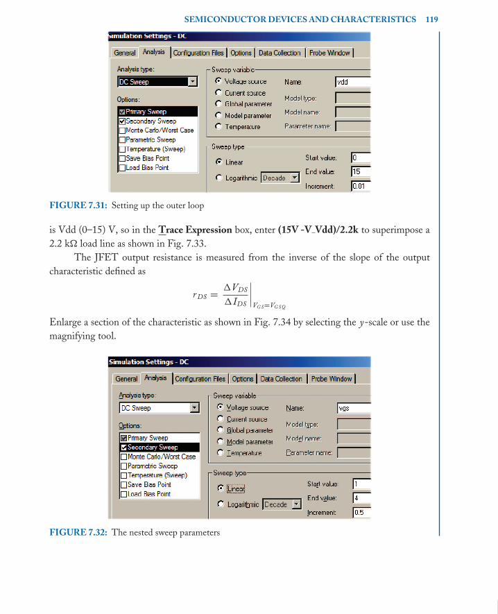
book Mobk059 March 9, 2007 10:21
SEMICONDUCTOR DEVICES AND CHARACTERISTICS 119
FIGURE 7.31: Setting up the outer loop
is Vdd (0–15) V, so in the Trace Expression box, enter (15V -V Vdd)/2.2k to superimpose a
2.2 k� load line as shown in Fig. 7.33.
The JFET output resistance is measured from the inverse of the slope of the output
characteristic defined as
r DS =1VDS
1IDS
∣
∣
∣
∣
VG S=VG SQ
Enlarge a section of the characteristic as shown in Fig. 7.34 by selecting the y-scale or use the
magnifying tool.
FIGURE 7.32: The nested sweep parameters

book Mobk059 March 9, 2007 10:21
120 PSPICE FOR CIRCUIT THEORY AND ELECTRONIC DEVICES
FIGURE 7.33: JFET output characteristic for a 1 k� load line
7.9.5 Effect of Temperature on the JFET Transfer CharacteristicSemiconductor devices behave differently over a range of temperature (Ludwig Boltzmann
1844–1906) values, so it is important to investigate circuit behavior for a temperature sweep
using the schematic in Fig. 7.35.
FIGURE 7.34: Enlarged section of the output characteristic

book Mobk059 March 9, 2007 10:21
SEMICONDUCTOR DEVICES AND CHARACTERISTICS 121
vdd
15v
+
-
vgs
5v
+
-
0
To sweep the temp
on the vgs char,
open up the setup
and using nested
sweep, set the temp
to -20 to 50 in steps
of 10 degrees
J2
gsd I
FIGURE 7.35: Investigating device change with temperature
From the Analysis tab menu, select DC Sweep and tick Temperature (Sweep) with
parameters as in Fig. 7.36.
Press OK, and the effects of temperature on the characteristic are displayed in Fig. 7.37.
Differentiating the drain current Ids = Ids s [1 − (Vgs /VP O )2], yields ⇒ d Ids
d Vgs= 2Ids s
−VP O(1 −
Vgs
VP O) = gm = gmo (1 − Vgs
VP O). The mutual conductance is a function of the gate source voltage
V gs and is measured from the transfer characteristic. In Probe, press the “Add a trace” icon
and the screen in Fig. 7.38 appears. Select the differential operator D( ) from the list
on the right, and in the brackets place the selected variable ID(J1) from the list on the
left.
FIGURE 7.36: Select temperature as the DC nested sweep
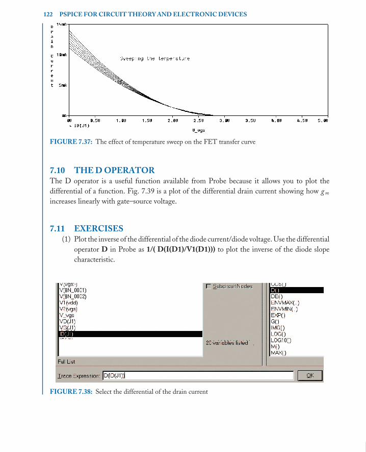
book Mobk059 March 9, 2007 10:21
122 PSPICE FOR CIRCUIT THEORY AND ELECTRONIC DEVICES
FIGURE 7.37: The effect of temperature sweep on the FET transfer curve
7.10 THE D OPERATORThe D operator is a useful function available from Probe because it allows you to plot the
differential of a function. Fig. 7.39 is a plot of the differential drain current showing how g m
increases linearly with gate–source voltage.
7.11 EXERCISES(1) Plot the inverse of the differential of the diode current/diode voltage. Use the differential
operator D in Probe as 1/( D(I(D1)/V1(D1))) to plot the inverse of the diode slope
characteristic.
FIGURE 7.38: Select the differential of the drain current

book Mobk059 March 9, 2007 10:21
SEMICONDUCTOR DEVICES AND CHARACTERISTICS 123
FIGURE 7.39: Differential of drain current
(2) In Fig. 7.40, investigate the diode turn on/off times using a VPULSE generator with
a very fast ±5 V pulse (I suggest TR = TF = 0.1ns, PW = 10 ns, PER = 20 ns). Plot
the diode current.
(3) Plot the Zener diode impedance in the different regions of the characteristic. Use the
D operator.
FIGURE 7.40: Measuring diode turn on/off times

book Mobk059 March 9, 2007 10:21
124 PSPICE FOR CIRCUIT THEORY AND ELECTRONIC DEVICES
FIGURE 7.41: The Table part
(4) Obtain the characteristics for the SCR and TRIAC devices. Download a model for the
unijunction transistor (UJT). This is a three-terminal device with different character-
istics to the conventional bipolar transistor. Construct a UJT circuit symbol, junction
schematic, and plot the output characteristics showing the negative resistance region.
(5) Investigate the TABLE part in Fig. 7.41. From the Analysis Setup/DC Sweep/Sweep
Variable /Voltage Source, Name = vin. The sweep parameters: Start Value: 0, End
Value 10V, and Increment 1.
(6) Investigate the BJT switching schematic in Fig. 7.42.
(7) Investigate the differential amplifier shown in Fig. 7.43.
(8) Investigate root locus plotting using DIFF and Laplace parts in Fig. 7.44. Analysis
tab to Analysis type: AC Sweep/Noise, AC Sweep Type to Logarithmic, Start
Frequency = 0.001, End Frequency = 10, Points/Decade = 10,001.
Press F11 to produce the locus plot shown in Fig. 7.45 but change the x-axis to
R(v(out)) and the y-axis to IMG(v(out)). Both of these functions are available from
Trace/Add Trace in Probe. However, in the latest edition of PSpice, there is now
FIGURE 7.42: BJT switch

book Mobk059 March 9, 2007 10:21
SEMICONDUCTOR DEVICES AND CHARACTERISTICS 125
FIGURE 7.43: Differential amplifier
Vin
1V +-
NUM = 24*(s-0.5)
DENOM = ((s+1)**2)*(s+2)
IN OUT
0
Out
V
FIGURE 7.44: A closed-loop control system
FIGURE 7.45: Change y-axis to IMG(v(out)) and x-axis to R(v(out))

book Mobk059 March 9, 2007 10:21
126 PSPICE FOR CIRCUIT THEORY AND ELECTRONIC DEVICES
a Nyquist sub routine plot which makes things very simple. After simulation, select
Trace/Add Trace and in the functions or macros window (top right hand corner),
select Nyquist Plot(1) and substitute V(Out) for the 1 in the brackets.
Make sure the x-axis Scale is Linear as the plot encompasses a zero value.

book Mobk059 March 9, 2007 10:21
127
C H A P T E R 8
Operational Amplifier Characteristics
8.1 IDEAL OPERATIONAL AMPLIFIERSThe normal operational amplifier (opamp) has two-input terminals and a single-output for
amplifying the voltage difference between the inverting and noninverting input terminals. An
ideal opamp has an infinite input impedance Ri = ∞�, zero output impedance Ro = 0 �, and
infinite gain, A. A nonideal op-amp has a very high input resistance, very low output resistance,
and a very high gain.
8.1.1 The Inverting Operational Amplifier and Virtual EarthFig. 8.1 shows a voltage-controlled voltage source (VCVS) E part (Analog.olb library) modeling
the operational amplifier in the linear range. The input impedance is set to 2 M�, with an
75 � output impedance but with no frequency limitations (see exercise 10 at the end of the
chapter). Apply a 1 VDC part and press F11 to simulate and display the bias conditions. A
very large gain 1010 produces a voltage at the junction of R1 and R2 of 477 pV, which is almost
FIGURE 8.1: An ABM op amplifier model

book Mobk059 March 9, 2007 10:21
128 PSPICE FOR CIRCUIT THEORY AND ELECTRONIC DEVICES
FIGURE 8.2: Open circuit opamp
zero. Hence, this point is called a virtual earth. This simple linear opamp model overcomes
the limitations of the evaluation version in a situation requiring a large number of operational
amplifiers (there is also an ideal opamp part available).
Draw the operational amplifier shown in Fig. 8.2.
The full gain of the ua741 operational amplifier is available in this comparator so that,
because of the large gain, a small input voltage will easily saturate the output to the rail
voltage. The transfer function characteristics may be read from the output file accessed from
the PSpice/View Output File menu, or from Probe/View.
Small signal characteristics
r V(Out)/V vin = 1.963E+05
r Input resistance at V vin = 9.963E+05
r Output resistance AT V(Out) = 1.494E+02
However, you must first select the Analysis Setup/Bias Point and set the Output File Options
as shown in Fig. 8.3. Out is the output wire segment name using the Net Alias icon explained
below, and the Input source name to Vin.
Use the Place Net Alias icon to place a name on a wire. When you open up this menu,
type the name out in the Alias box as shown in Fig. 8.4. This produces a little square which
must be dragged over to the wire segment and placed accurately on the wire. The wire segment
must be long enough to accommodate the name.
Draw the inverting amplifier shown in Fig. 8.5.
To investigate noise analysis for the circuit in Fig. 8.5, set the parameters as shown in
the insert menu and run an AC analysis. To list the main noise contributors, open the output
file from Probe.

book Mobk059 March 9, 2007 10:21
OPERATIONAL AMPLIFIER CHARACTERISTICS 129
FIGURE 8.3: Transfer function characteristics
FIGURE 8.4: Placing a wire alias name
FIGURE 8.5: Inverting mode opamp

book Mobk059 March 9, 2007 10:21
130 PSPICE FOR CIRCUIT THEORY AND ELECTRONIC DEVICES
FIGURE 8.6: Slew rate limiting
8.1.2 Slew Rate LimitingThe VSIN part has Freq set to 100 kHz, VAMP = 1 V (A peak value), and VOFF = 0.
⌈Note there is no space between the variable value and the dimensions, i.e. 100k, not 100 k
as this will produce an error “ERROR – Expecting keyword STIMULUS, saw k”⌉. Carry out
a transient analysis with Run to time = 50 us, Maximum step size = 100 n and compare
the slewed output signal in Fig. 8.6 to the input sine wave. Simulating a schematic produces
several files, one of which is the Probe output called Figure 8-005.dat which when selected
from Probe should produce a blank screen, so click Trace/Add Trace, and select the output
signal (Or press the Insert key).
Use the Place Net Alias icon to name a wire segment vout. To measure the output
distortion for different input voltages, open the Analysis Setup/Transient menu. Place a tick
on Perform Fourier Analysis, Center frequency = 100 k, Number of Harmonics = 10,
and Output Variables: = v(vout). From Probe, select the icon from the left-hand toolbar to
examine the harmonic analysis information at the end of the .out text file.
8.2 THE NONINVERTING OPERATIONAL AMPLIFIERThe gain for the noninverting configuration shown in Fig. 8.7 is
Avc = Vout/Vin (8.1)
β is a portion of the output fed back from the output to the input. The output voltage is
Vout = A(Vin − βVout) = AVin − β AVout ⇒ Vout(1 + β A) = AVin (8.2)

book Mobk059 March 9, 2007 10:21
OPERATIONAL AMPLIFIER CHARACTERISTICS 131
FIGURE 8.7: Noninverting configuration
Av =Vout
Vin=
A
1 + β A(8.3)
If the open–loop gain is large then we may write (8.3) as
Av =1
1/A + β≈
1
0 + β≈
1
β(8.4)
The feedback factor is
β =Rb
Rb + Ra⇒ Av ≃
1
β≃
Rb + Ra
Rb= 1 +
Ra
Rb(8.5)
8.2.1 Gain–Bandwidth ProductA PARAM part investigates the concept of GAIN–BANDWIDTH product and shows how
the gain and bandwidth parameters are interlinked i.e. if the gain is reduced then the bandwidth
increased and vice versa.
Rclick the PARAM part, select Edit Properties and add a new row with Ra entered
in the first column and 1k in the second column. Go back to the schematic and select the
resistance Ra and enter {Ra} rather than an actual resistance value. We wish to carry out a
frequency response for the different values of the resistor to be swept, so select the Analysis
tab from the simulation icon and select Analysis type: AC Sweep/Noise, AC Sweep Type
to Linear, Start Frequency = 10, End Frequency = 1000k, Points/Decade = 1000. Tick
Parametric Sweep in the Options menu and set the parameters shown in Fig. 8.8. Enter the
values for Ra in the Value List with each value separated by a space.

book Mobk059 March 9, 2007 10:21
132 PSPICE FOR CIRCUIT THEORY AND ELECTRONIC DEVICES
FIGURE 8.8: Using Param and list
Press F11, and a Probe screen message “Available Sections” appears. Select OK to plot
the frequency response as shown in Fig. 8.9. Measure the passband gain and –3 dB point on
each response.
The gain–bandwidth product is investigated using Performance Analysis (PA) available
in Probe/Trace menu. PA allows you see how a characteristic, such as the gain bandwidth
FIGURE 8.9: Noninverting frequency response

book Mobk059 March 9, 2007 10:21
OPERATIONAL AMPLIFIER CHARACTERISTICS 133
FIGURE 8.10: GB product using Performance Analysis
product in this case, varies when the feedback resistor, Ra is varied. Simulate the previous
schematic, and from the Probe output, press ok from Available Sections. Press the PA icon
(Two crossed flags) and a further menu headed Performance Analysis appears, so press OK.
Select the Trace Add icon and enter Cutoff Lowpass 3dB(V(vout))*Max(V(vout)) in the
Trace Expression box to produce the display in Fig. 8.10.
8.3 AUDIO POWER AMPLIFIERSNPN and PNP power transistor symbols are created using the QbreakN and QbreakP parts
from the break library. Place QbreakN and QbreakP parts on a new schematic area. Select
one of these symbols and it should turn green. Rclick, and select Edit Properties from the list.
From this properties menu, select QbreakN in the second column and replace it with TIP31.
Select the Display icon to get the Design Properties menu where the name is entered as shown
in Fig. 8.11. Tick Name and Value to display the name and value on the schematic. Press OK
Select the transistor and Rclick. From the displayed list, select Edit Pspice Model to run the
PSpice Model Editor. The demo version will not allow you to save the new power transistor
however, but if you are using the full version then you can save it to yourcircuitname.lib. Save
the results by selecting Part and Save to Library. The contents of the .lib file are shown in
Fig. 8.12.
The first line is the model name. However, we can still use the power transistor from
MYLIB.lib that was added previously. Repeat this procedure for the TIP32 power transistor
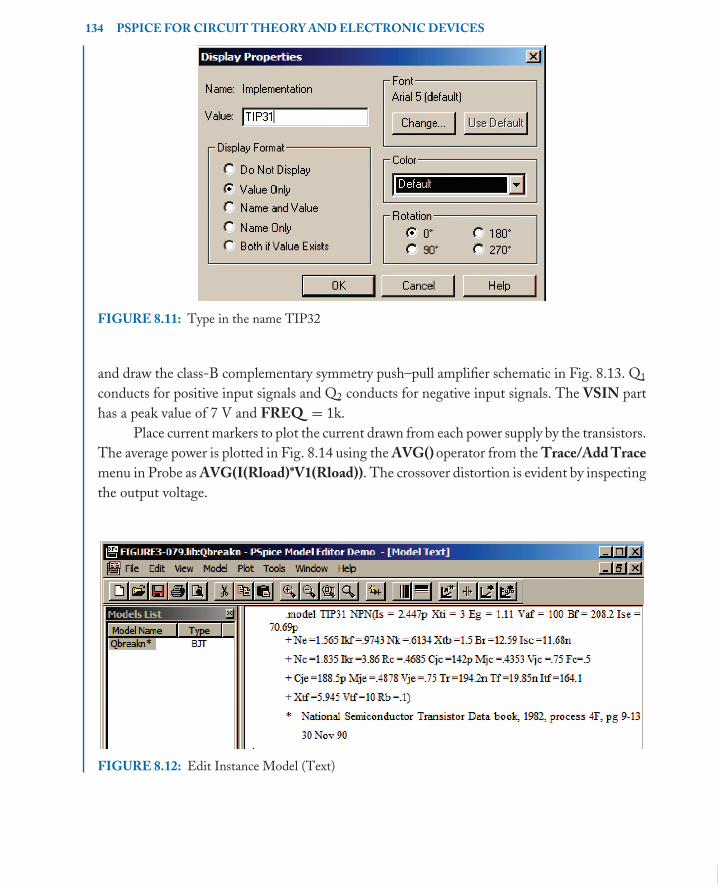
book Mobk059 March 9, 2007 10:21
134 PSPICE FOR CIRCUIT THEORY AND ELECTRONIC DEVICES
FIGURE 8.11: Type in the name TIP32
and draw the class-B complementary symmetry push–pull amplifier schematic in Fig. 8.13. Q1
conducts for positive input signals and Q2 conducts for negative input signals. The VSIN part
has a peak value of 7 V and FREQ = 1k.
Place current markers to plot the current drawn from each power supply by the transistors.
The average power is plotted in Fig. 8.14 using the AVG() operator from the Trace/Add Trace
menu in Probe as AVG(I(Rload)*V1(Rload)). The crossover distortion is evident by inspecting
the output voltage.
FIGURE 8.12: Edit Instance Model (Text)

book Mobk059 March 9, 2007 10:21
OPERATIONAL AMPLIFIER CHARACTERISTICS 135
FIGURE 8.13: Push–pull amplifier
A power amplifier converts the DC input power to useful AC output power but in the
process of doing this some power is dissipated in the circuit components. We need to consider
the input power, the output power, and the power wasted in the circuit. The amplifier efficiency
is calculated by considering the maximum input and output powers, and the maximum transistor
power dissipation. A sinusoidal test signal is applied to the amplifier and we must consider the
power in the load. The peak output voltage across the load RL is Vp , then the output current
is Ip = Vp/RL. The maximum output power (RMS) is Po = Vp√2
Ip√2
= V 2p
2RL. If we assume ideal
FIGURE 8.14: Class-B push–pull power amplifier

book Mobk059 March 9, 2007 10:21
136 PSPICE FOR CIRCUIT THEORY AND ELECTRONIC DEVICES
transistors, then the output power is Po = V 2c c
2RL. The average value for a sinusoidal test signal
over half a period (T/2 = π ) is
Vav =1
T
T/2∫
0
Vp sin(2π ft)dt = −Vp
T
[
cos(2π ft)
2π f
]T/2
0
= −Vp
2π[cos(π ) − cos(0)] =
Vp
π(8.6)
The average single-line power supply current is Iav = (2Vp/π )/RL, hence the total average
power from the source is Ps = Vc c Iav = Vc c (2Vp/π )/RL. The efficiency is the ratio of output
to input power as a percentage as
η =Po
Ps=
(
V 2p /2RL
)
Vc c (2/π )(Vp/RL)× 100 % =
π
4
Vp
Vc c× 100 % (8.7)
The maximum efficiency for class-B operation with Vp = Vc c is η = π4
Vc c
Vc c× 100 % = 78.54 %.
The power dissipation for each transistor is the difference between the supply power and the
power dissipated in the load:
PD = Ps − Po = Vc c2
π
Vp
RL−
V 2p
2RL(8.8)
Differentiate (8.8) with respect to V p and equate to zero. This gives the maximum transistor
power dissipation P D(max) d PD
d Vp= 2
π
Vc c
RL− Vp
RL= 0. If Vp = 2Vc c /π , then (8.8) yields
PD(max) =2
π
2
π
V 2c c
RLVc c −
4
π2
V 2c c
2RL=
2
π2
V 2c c
RL≈ 0.2
V 2c c
RL(8.9)
The total amplifier dissipation is PD(max) = 0.4Po (max), so the average power for each
transistor is PD(max) = 0.2o (max). Set Analysis to Analysis type: Time Domain (Transient),
Run to time = 3ms, and Maximum step size = 1us, Press F11 to observe the crossover
distortion shown in Fig. 8.15.
8.3.1 The Output FilePress the FFT icon to show the distortion harmonics due to cross-over distortion. Measure
each harmonic Dn and insert into the expression %total =√
D21 + D2
2 + D23 + · · ·, to give an
approximate percentage distortion. Alternatively, measure the percentage harmonic distortion
by selecting the output file icon in Probe (located on the icon toolbar at the left). Measure
the distortion by naming the output wire VO and setting the parameters in the Transient/
Fourier analysis menu as: Perform Fourier Analysis, Center Frequency = 1k, Number of
Harmonics = 10, and Output Variables = v(VO). The results of this analysis are found at

book Mobk059 March 9, 2007 10:21
OPERATIONAL AMPLIFIER CHARACTERISTICS 137
FIGURE 8.15: Crossover distortion
the end of the output file shown below (opened from the Analysis menu, or the View menu in
Probe).
FOURIER COMPONENTS OF TRANSIENT RESPONSE V(VO)DC COMPONENT = 7.156562E+00HARMONIC FREQUENCY FOURIER NORMALIZED PHASE NORMALIZEDNO (HZ) COMPONENT COMPONENT (DEG) PHASE (DEG)
1 1.000E+03 4.970E+0 1.000E+0 4.770E−01 0.000E+002 2.000E+03 1.347E−03 2.711E−04 −1.506E+02 −1.511E+023 3.000E+03 8.964E−05 1.804E−05 −1.398E+02 −1.403E+024 4.000E+03 1.990E−04 4.004E−05 1.736E+02 1.732E+025 5.000E+03 1.631E−04 3.282E−05 1.764E+02 1.760E+026 6.000E+03 1.331E−04 2.677E−05 1.756E+02 1.752E+027 7.000E+03 1.139E−04 2.292E−05 1.748E+02 1.744E+028 8.000E+03 9.921E−05 1.996E−05 1.740E+02 1.735E+029 9.000E+03 8.806E−05 1.772E−05 1.737E+02 1.732E+02
10 1.000E+04 7.833E−05 1.576E−05 1.730E+02 1.725E+02
TOTAL HARMONIC DISTORTION = 2.805018E-02 PERCENT
Compare the total harmonic distortion of 2.8 % to that calculated using % distortion =√
D21 + D2
2 + D23 + .... The previous circuit is modified to include a trickle bias as shown in
Fig. 8.16. This quasi-complimentary push–pull amplifier has the output transistors connected in
a Darlington pair configuration to reduce crossover distortion and yield lower output impedance
values.

book Mobk059 March 9, 2007 10:21
138 PSPICE FOR CIRCUIT THEORY AND ELECTRONIC DEVICES
FIGURE 8.16: Improved power amplifier design
Make Rt variable in order to investigate crossover distortion. Change it from 47 k� to
{rvar}, and place a Param part to define the name and value. The average power is plotted in
Fig. 8.17 using the AVG( ) operator from the Trace/Add Trace (or the insert button) function
in Probe.
8.4 MOSFET DEVICE CHARACTERISTICDraw the MOSFET schematic shown in Fig. 8.18.
Set vdd to 5 V, and sweep vg from 0 V to 5 V to plot the transfer characteristic shown in
Fig. 8.19.
Fig. 8.20 shows the output characteristic obtained by setting the Primary Sweep vdd
from 0 to 5 V in steps of 0.1 V, and the Secondary Sweep vg from 0 to 6 V in steps
of 0.5 V.
Draw the complimentary symmetry metal oxide (CMOS) schematic in Fig. 8.21.
The breakout symbol models Mbreakp3 and MbreakN3 are then associated with the
two models listed in the comments in Section 8.4.1. Sweep vin from 0 to 5 V, in steps of 0.001,
Press F11 to simulate and plot the vin/vout characteristic shown in Fig. 8.22.
This characteristic shows that when the input level has a high positive value it causes the
PMOS to turn off and the NMOS to turn on, thus making the output go to 0 V. When the

book Mobk059 March 9, 2007 10:21
OPERATIONAL AMPLIFIER CHARACTERISTICS 139
FIGURE 8.17: Average power output
input level is low, it causes the PMOS to turn on and the NMOS to turn off, which results in
the output going high i.e. 5 V.
8.4.1 CMOS ModelThe model for the MbreakP3 part is
.MODEL NCH NMOS (level=2 LD=0.15U TOX=200.0E−10 NSUB=5.37E+15+ VTO=0.74 KP=8.0E−05 GAMMA=0.54 PHI=0.6 U0=656 UEXP=0.157 UCRIT=31444+ DELTA=2.34 VMAX=55261 Xj=0.2U LAMBDA=0.037 NFS=1E+12 NEFF=1.001 NSS=1E+11+ TPG=1.0 RSH=70.00+ CGDO=4.3E−10 CGSO=4.3E−10 Cj=0.0003 Mj=0.66+ CJSW=8.0E−10 MJSW=0.24 PB=0.58
vg1v
+
-
vdd
9v
+
-M1
IRF9140
0
IRF150=n-channel mosfet- enhancement
IRF140=p-channel mosfet- enhancement
I
FIGURE 8.18: MOSFET circuit

book Mobk059 March 9, 2007 10:21
140 PSPICE FOR CIRCUIT THEORY AND ELECTRONIC DEVICES
FIGURE 8.19: Transfer characteristic
FIGURE 8.20: Output characteristic

book Mobk059 March 9, 2007 10:21
OPERATIONAL AMPLIFIER CHARACTERISTICS 141
vdd
5v
+
-
vin1v
+
-
M4
PCH
M3
NCH
out
0
V
FIGURE 8.21: CMOS inverter
The model for the MbreakN3 part is
.MODEL PCH PMOS(level=2 LD=0.15U TOX=200.0E−10 NSUB=4.33E+15+ VTO=−0.74 KP=2.70E−05 GAMMA=0.58 PHI=0.6 U0=262 UEXP=0.324 UCRIT=65720+ DELTA=1.79 VMAX=25694 Xj=0.25U LAMBDA=0.061 NFS=1E+12 NEFF=1.001 NSS=1E+11+ TPG=1.0 RSH=121.00+ CGDO=4.3E−10 CGSO=4.3E−10 Cj=0.0005 Mj=0.51+ CJSW=1.35E−10 MJSW=0.24 PB=0.64
FIGURE 8.22: A plot of the input voltage versus the output voltage

book Mobk059 March 9, 2007 10:21
142 PSPICE FOR CIRCUIT THEORY AND ELECTRONIC DEVICES
FIGURE 8.23: Two-input NAND gate
8.4.2 Nand GateDraw the two-input NAND gate schematic shown in Fig. 8.23 using the CMOS devices
investigated in the previous section. Included in the schematic is a 7400 part for comparison
purposes.
A 100 pF capacitor on the output eliminates spikes in the output waveform. To test
the gate, apply two STIM generator parts to the two inputs. The STIM parts’ param-
eters are shown in Fig. 8.24. The startloop command loops to produce an infinite test
string.
The NAND gate truth table is shown in Table 8.1. Here we see that there is no output
when the two inputs are identical but the output goes high for all other combinations.
FIGURE 8.24: STIM1 and STIM2 parameters

book Mobk059 March 9, 2007 10:21
OPERATIONAL AMPLIFIER CHARACTERISTICS 143
TABLE 8.1: NAND Gate
A B C
0 0 1
0 1 1
1 0 1
1 1 0
Comparing our model to an existing two-input 7400 NAND part shows how the “home-
made gate” gives comparable results, as shown in Fig. 8.25.
8.4.3 Nor GateDraw the NOR gate schematic displayed in Fig. 8.26, and compare its performance to a
standard 7402 NOR part.
The two-input NOR gate truth table in Table 8.2 shows an output present only when
the two inputs are different.
Press F11 to simulate and produce the gate waveforms that are displayed in Fig. 8.27.
FIGURE 8.25: NAND gate waveforms

book Mobk059 March 9, 2007 10:21
144 PSPICE FOR CIRCUIT THEORY AND ELECTRONIC DEVICES
TABLE 8.2: Nor Gate
A B C
A B C
0 0 1
0 1 0
1 0 0
1 1 0
8.5 EXERCISES(1) Fig. 8.28 shows a schematic for obtaining the ua741 offset characteristics: The input
offset voltage is the input voltage required to bring the output voltage to zero with zero
signal voltage applied. The maximum, or short-circuit current output is obtained using
a small output resistance (1 u�), and plotting the output current.
To measure the offset voltage (mV), make all the parameters of the VSIN part zero and
do a DC sweep from –1mV to +1mV, in steps of 0.1uV. This should produce a graph
showing the output voltage saturating at ± rail voltage, but with a positive sloping part
in the middle of the plot. The offset voltage is the input voltage necessary to make the
output voltage zero as shown from the response in Fig. 8.29. The open-loop gain is
measured from the slope of the graph. In a real ua741 circuit, a potentiometer is placed
FIGURE 8.26: A two-input NOR gate

book Mobk059 March 9, 2007 10:21
OPERATIONAL AMPLIFIER CHARACTERISTICS 145
FIGURE 8.27: Two-input NOR gate waveforms
across the offset adjusting pins and then connected to the negative supply where it is
adjusted to reduce offsets. These pins are displayed in the PSpice ua741 symbol, but
are not actually modeled.
Measure the input bias current by pressing the “I” icon but with both inputs grounded
to earth.
FIGURE 8.28: Open-loop measurements

book Mobk059 March 9, 2007 10:21
146 PSPICE FOR CIRCUIT THEORY AND ELECTRONIC DEVICES
FIGURE 8.29: The open-loop transfer function
(2) To measure the input and output impedances, follow the procedure outlined in [ref:
3]. Measure the output impedance by injecting a voltage as shown and plotting the
ratio of voltage/current as shown in Fig. 8.30.
(3) Investigate the opamp open-loop gain characteristics using the schematic shown in
Fig. 8.31.
The response should be similar to that shown in Fig. 8.32.
(4) Investigate the Schmitt trigger circuit shown in Fig. 8.33. A VPWL part generates a
saw-toothed signal to sweep the input.
The reference voltage Vref = Vo R1/(R1 + R2) = 14.6.1k/(1k + 10k) = 1.3 V. Mea-
sure the slew rate and compare to the ua741 specification. Change the x-axis to
FIGURE 8.30: The output impedance

book Mobk059 March 9, 2007 10:21
OPERATIONAL AMPLIFIER CHARACTERISTICS 147
FIGURE 8.31: Noninverting op amp
Vin, and press Alt PP for a new upper plot axis in time as in Fig. 8.34 (select the
Plot/Unsynchronize X-Axis menu for the upper plot). This is equivalent to changing
the oscilloscope time base to the X − Y mode and connecting a triangle wave from
a function generator to the x-plates. Modify Fig. 8.33 to produce the circuit in Fig.
8.35. The hysterisis diagram shown in Fig. 8.36 is now plotted in the reverse direction
when compared to Fig. 8.34. Add a noise generator in series with vsweep to verify the
effectiveness of hysterisis.
FIGURE 8.32: Gain-Bandwidth product

book Mobk059 March 9, 2007 10:21
148 PSPICE FOR CIRCUIT THEORY AND ELECTRONIC DEVICES
FIGURE 8.33: Schmitt-trigger circuit
(5) Investigate the astable oscillator using a ua741 IC in Fig. 8.37. The circuit to the right
is for comparing the charging capacitors in each circuit.
The frequency of the square wave is calculated as
f0 =1
2C R3 ln[2(R2/R1) + 1](8.10)
(6) To reduce crossover distortion, modify the previous circuit by adding transistors con-
figured as diodes to achieve trickle bias as shown in Fig. 8.38 [Ref: 5 Appendix A].
FIGURE 8.34: Schmitt trigger hysterisis

book Mobk059 March 9, 2007 10:21
OPERATIONAL AMPLIFIER CHARACTERISTICS 149
FIGURE 8.35: Schmitt trigger
The waveforms for this improved amplifier are shown in Fig. 8.39.
(7) Investigate the operational amplifier model using ABM parts shown in Fig. 8.40. The
operational amplifier transfer function is entered in the Laplace part as a low-pass filter
with a 30 rs−1 cut-off frequency (pole frequency f c = 4.78 Hz). The Diff part sums
the input signals and the Gain part represents the very large open-loop gain of 100 k.
FIGURE 8.36:

book Mobk059 March 9, 2007 10:21
150 PSPICE FOR CIRCUIT THEORY AND ELECTRONIC DEVICES
FIGURE 8.37: Astable oscillator
FIGURE 8.38: Improved power amplifier

book Mobk059 March 9, 2007 10:21
OPERATIONAL AMPLIFIER CHARACTERISTICS 151
FIGURE 8.39: Power amplifier signals
The limit part limits the output to a value a little below the power supply value. We
could use the Glimit part (contains the gain and limit parts) [ref: 4].
(8) The schematic in Fig. 8.41 uses the very good specification AD8041 opamp. Select the
resistor R2 and enter the value {Rgain}. Place and select a Param part from the Special
library. Highlight NAME1, and enter Rgain in the Value box. Similarly, select the
VALUE1 attribute, and enter 1k in the Value box. From the Analysis Setup menu,
selectParametric, and in that sub menu, define Name = Rgain, Start Value = 1k,End
Value = 100k, and Increment = 20k.
The frequency response in Fig. 8.41 shows how the AD8041 is a much superior op
amplifier with a much larger passband frequency range compared to the very poor
ua741 op amp frequency response.
FIGURE 8.40: Constructing an opamp from ABM parts

book Mobk059 March 9, 2007 10:21
152 PSPICE FOR CIRCUIT THEORY AND ELECTRONIC DEVICES
FIGURE 8.41: Inverting op amp
FIGURE 8.42: Frequency response
Anytime you get results that are unexpected, or the results don’t agree with your
calculations, suspect the limitations of the ua741 and substitute a better device such as
the AD8041.
REFERENCES[1] P. Tobin, PSpice for Filters and Transmission Lines. Morgan Claypool publishers (Feb
2007).

book Mobk059 March 9, 2007 10:21
OPERATIONAL AMPLIFIER CHARACTERISTICS 153
[2] P. Tobin, (2007) PSpice for Digital Signal Processing. San Rafael, CA: Morgan Claypool,
2007.
[3] P. Tobin, PSpice for Analog Communications Engineering. San Rafael, CA: Morgan
Claypool, 2007.
[4] M. E. Herniter Merrill, Schematic Capture with PSpice. New York: Macmillan, 1994.
[5] OrCAD PSpice for Windows, Volume II: Devices, Circuits, and Operational Amplifiers
(3rd Edition) (Paperback) by Roy W. Goody New Jersey.
[6] Tobin Paul, PSpice for Digital Communications Morgan Claypool publishers Feb 2007.

book Mobk059 March 9, 2007 10:21
154 PSPICE FOR CIRCUIT THEORY AND ELECTRONIC DEVICES
APPENDIX A: LAPLACE AND z-TRANSFORM TABLE
LAPLACE z-TRANSFORM
FUNCTION f (t) TRANSFORM f (n) (t = nT = n)
Unit step u(t)1
su(n)
z
z − 1
Unit impulse δ(t) 1 δ(n) 1
Unit ramp T1
s 2N
nz
(z − 1)2
Polynomial tn n!
s n+1tn T2z(z + 1)
(z − 1)2for n = 2
Decaying e−at 1
(s + a)e−anu(n)
z
z − e−an
exponential
Growing1
a(1 − e−at)
1
(s + a)(s )
1
a(1 − e−an)
z(1 − e−an)
a(z − 1)(z − e−an)exponential
Sine sin(ωt)ω
(s 2 + ω2)sin(nθ )u(n)
z sin nθ
z2 − 2z sin nθ + 1
Cosine cos(ωt)s
(s 2 + ω2)cos(nθ )u(n)
z(z − cos nθ )
z2 − 2z cos nθ + 1
Damped sine e−at sin(ωt)ω
[(s + a)2 + ω2)]e−an sin(nθ )
ze−an sin(nθ )
z2 − 2ze−an cos nθ + e−2an
Damped cosine e−at cos(ωt)(s + a)
[(s + a)2 + ω2)]e−an cos(nθ )
z2 − ze−an cos(nθ )
z2 − 2ze−an cos nθ + e−2an
Delay f (t − k) e−s k f (n − k) z−k

book Mobk059 March 9, 2007 10:21
155
Index
abc icon, 6
abm part, 149
add a load line, 116
add a trace icon, 121
admittance, 20
agnd, 7
analysis menu, 59, 62
analysis setup icon, 112
analysis setup menu, 9, 13
apparent power, 96
append file, 69
assigned current direction, 19
astable oscillator, 148
average power, 95
avg() operator, 138
bandwidth (1, dB), 84
bias point, 21
BJT switch, 124
Boltzmann constant, 101
capacitive reactance, 53
capacitor, 3
charge , 53
clipping, 117
coefficient of coupling, 89
complex conjugate, 60
crossover distortion, 148
current divider, 11
current marker, 6
current probe, 115
cursor icon, 16
cursor peak, 16
d-operator, 122
Darlington connection, 137
3 dB bandwidth, 72
dc nested sweep, 112
dc sweep, 13, 112, 115
decade, 83
diff part, 149
differential, 122
differential voltage markers, 69
diode characteristic, 101
displayed precision, 21
dynamic impedance, 84
e part, 48
e- part, 127
Edit Simulation Settings, 13
elaplace part, 38
error voltage source, 57
evaluate measurement, 46
evaluate measurement function, 84
exponentially- decaying sinusoidal, 37
FFT, 77
FFT resolution, 77
FFT:, 44
file menu, 1
first-order circuit, 24
flipping a component, 4

book Mobk059 March 9, 2007 10:21
156 PSPICE FOR CIRCUIT THEORY AND ELECTRONIC DEVICES
floating error, 7, 88
Fourier series expansion, 74
gain-bandwidth product, 131
get parts icon, 6
glimit part, 149
ground bounce, 91
ground symbol, 7
idc part, 11
ideal, 78
ideal current source, 82
if then else, 51
imaginary part, 62
increments, 9
inductor, 24
inductor loop involving V Vs, 57
initial voltage, 23
input characteristic, 110
input offset voltage, 144
instantaneous power, 94
inverting amplifier, 128
iprint1 part, 60
isin part, 62
j2n3819, 114
K3019PL 3C8, 89
K502T300 3C8, 89
K528T500 3C8, 89
K Linear, 89
Laplace part, 149
Laplace transform, 23
linear sweep, 9, 71
linear to log icon, 16
loaded Q-factor, 82
magnetic coupling, 88
magnifying tool, 83
mark voltage differential, 25
markers menu, 25
maximize the schematic, 1
maximum power, 16
maximum power transfer, 60, 89
maximum step size, 76
mesh and nodal analysis, 62
mesh currents, 18
multi-winding transformer, 90
mutual admittance, 20
mutual impedance, 18
name box, 9
NAND, 142
nested DC sweeps, 110
New Simulation Profile, 13
no print delay, 76
non-ideal op-amp, 127
NOR, 143
nor, 143
Norton equivalent circuit, 24, 62
Ohm’s law, 6
operational amplifier, 127, 130
oscilloscope probe, 48
output file, 62
parallel-tuned circuit, 77, 82
param part, 48, 70, 151
param’ part, 4, 13
part name, 3
partial fraction expansion, 26, 33
passband gain, 132
periodic function, 74
piece-wise linear generator, 37

book Mobk059 March 9, 2007 10:21
INDEX 157
pinch-off voltage, 117
Place Net Alias, 128
places of decimals, 20
potential divider, 9
potential division, 88
power dissipation, 107
power factor, 95
power supplies, 91
power supply decoupling, 92
primary turns, 89, 91
Q-factor, 72
Q-point, 114
quasi-complimentary push–pull, 137
quiescent DC point, 117
Reactive power, 97
regulation, 107
resistive loading, 12
resonant frequency, 72
reverse breakdown region, 104
reverse saturation current, 101
ripple voltage, 91
rise-time, 92
risetime, 46
root locus plot, 124
rvar, 71
skip initial transient solution, 45
saturation current, 121
secondary, 89, 91
self admittance, 20
self-impedance, 18
series-tuned circuit, 65, 70, 74
short-circuit current, 144
shortcut commands, 6
significant digits, 20
silicon-controlled rectifier, 107
skip initial conditions, 76
slope, 114
step function, 23
susceptance, 57
sweep type, 9
symmetrical signal swing, 117
table part, 124
tee-network, 18
temperature sweep, 121
Thevenin equivalent circuit, 28
Thevenin equivalent impedance, 60
Thevenin voltage, 61
thyristor, 107
TIP32 power transistor, 133
to copy an element , 6
to discontinue using element, 6
to paste element, 6
to rotate a component , 6
toolbar icons, 1
trace add, 130
trace add icon, 15
trace expression box, 15, 47, 116
trace menu, 56, 116
transfer conductance, 114
transfer function, 9
transformer, 89
true rms meter, 51
turns-ratio, 91
two-port network, 10
ua741, 3
UJT, 124
v and i icons, 11, 20
variable capacitor, 49

book Mobk059 March 9, 2007 10:21
158 PSPICE FOR CIRCUIT THEORY AND ELECTRONIC DEVICES
VARS, 99
VCVS, 127
voffset, 117
voltage piece-wise linear vpwl, 107
voltage regulator, 106
voltage-controlled voltage source,
127
vprint1 part, 59
vpulse generator, 123
vpulsepart, 42
vpwl generator, 39
vrsc part, 101
vsin generator, 55
vsin part, 59
w, 4
wildcard, 3
wire tool, 6
x-axis variable, 101
xform, 41
XFRM LINEAR, 89
XFRM NONLINEAR, 89
zener diode, 105

book Mobk059 March 9, 2007 10:21
159
Author Biography
Paul Tobin graduated from Kevin Street College of Technology (now the Dublin Institute of
Technology) with honours in electronic engineering and went to work for the Irish National
Telecommunications company. Here, he was involved in redesigning the analogue junction
network replacing cables with PCM systems over optical fibres. He gave a paper on the design
of this new digital junction network to the Institute of Engineers of Ireland in 1982 and was
awarded a Smith testimonial for one of the best papers that year. Having taught part-time
courses in telecommunications systems in Kevin Street, he was invited to apply for a full-time
lecture post. He accepted and started lecturing full time in 1983. Over the last twenty years he
has given courses in telecommunications, digital signal processing and circuit theory.
He graduated with honours in 1998 having completed a taught MSc in various DSP
topics and a project using the Wavelet Transform and neural networks to classify EEG (brain
waves) associated with different mental tasks. He has been a ‘guest professor’ in the Institut
Universitaire de Technologie (IUT), Bethune, France for the past four years giving courses in
PSpice simulation topics. He wrote an unpublished book on PSpice but was persuaded by Joel
Claypool (of Morgan and Claypool Publishers) at an engineering conference in Puerto Rico
(July 2006), to break it into five PSpice books. One of the books introduces a novel way of
teaching DSP using PSpice. There are over 500 worked examples in the five books covering
a range of topics with sufficient theory and simulation results from basic circuit theory right
up to advanced communication principles. Most of these worked example circuit have been
thoroughly ‘student tested’ by Irish and International students and should mean little or no
errors but alas. . . He married Marie and had four grown sons and his hobbies include playing
modern jazz on double bass and piano but grew up playing G-banjo and guitar. His other
hobby is flying and obtained a private pilots license (PPL) in the early 80’s.

book Mobk059 March 9, 2007 10:21