overview of optoelectronic devices and materials research group (odm) alf adams optoelectronic...
TRANSCRIPT

abcdefghijklm
Overview of Optoelectronic Devices and Materials
Research Group (ODM)
Alf Adams
Optoelectronic Devices and Materials Research Group
Tel +44 (0)1483 879310Fax +44 (0)1483 876781
abcdefghijklm
University of Surrey
School of Physics and Chemistry
Guildford, SurreyGU2 7XH, UK
abcdefghijklm
Overview of Optoelectronic Devices and Materials
Research Group (ODM)
Eoin O’Reilly
Optoelectronic Devices and Materials Research Group
Tel +44 (0)1483 876785Fax +44 (0)1483 876781
abcdefghijklm
University of Surrey
School of Physics and Chemistry
Guildford, SurreyGU2 7XH, UK
abcdefghijklm
Overview of Optoelectronic Devices and Materials
Research Group (ODM)
Jeremy Allam
Optoelectronic Devices and Materials Research Group
Tel +44 (0)1483 876799Fax +44 (0)1483 876781
abcdefghijklm
University of Surrey
School of Physics and Chemistry
Guildford, SurreyGU2 7XH, UK

abcdefghijklm
Overview of Optoelectronic Devices and Materials
Research Group (ODM)
Optoelectronic Devices and Materials Research Group
Tel +44 (0)1483 876800Fax +44 (0)1483 876781
abcdefghijklm
University of Surrey
School of Physics and Chemistry
Guildford, SurreyGU2 7XH, UK

abcdefghijklm
ODM quotes...
• Exploring the fundamental physics of laser-matter interactions, developing new materials for photonics and advanced optics.
• We do experiment and theory with rigour and vigour A.R. Adams, FRS
• Fun and innovative science, plus the bonus of a massive (well-paid) jobs boom in photonics/laser science
Take the challenge, ODM
• Although less than one PhD in 12 specializes in optics/lasers, this subfield accounted for almost one-fourth of the potentially permanent positions outside of academia
Recently released employment report, American Institute of Physics

abcdefghijklm
III-N and II-VI materials
Visible wave-
lengths: displays
• III-N materials (AlN, GaN, InN) for blue light emitters
• “dilute nitrides” (GaNAs, GaInNAs) are promising for the infrared (large bowing gives small bandgap)

abcdefghijklm
Bandstructure of zincblende semiconductors
• not only the bandgap, but also energies of ‘critical points’ in the bandstructure (E, EL, EX) are important for optoelectronic device performance

abcdefghijklm
Conventional III-V semiconductors
1.3 µm, 1.55µm telecoms bands
• GaInAs lattice-matched to InP dominates applications in optical telecoms

abcdefghijklm
Semiconductor Materials
B O
In
C
Si
Ge
Sn
N
Al P
Ga As
Sb
Se
S
Zn
TeCd
III IV V VIII
2
3
4
5
per
iod
groupCommon tetrahedral
(zincblende) semconductors:
group IVIII-VII-VI
• Silicon is ubiquitous in electronics, but interacts relatively weakly with light
• direct-gap III-V’s are used for light emission and detection in the visible and near-infrared

abcdefghijklm
The Physics Department will be hosting a
Postgraduate Recruitment Fair
on Wednesday 13th Februaryat 16:00 in 7AC05 and corridors
including at 17:15 a short talk on ‘Research Opportunities and Funding’ by Prof. Tostevin
Come and find out about opportunities for PhD or Masters degrees in the Department of Physics and
related departments in the University of Surrey.
Other local Universities have also been invited.
To all students graduating in 2002

abcdefghijklm
ODM: world leaders in …
• use of hydrostatic pressure to investigate physical
• processes in semiconductors and optoelectronic devices
• elucidation of loss mechanisms in semiconductor lasers
• design and characterisation of strained-layer quantum well lasers
• theory of strained quantum dots
• understanding physical properties of dilute nitrides

abcdefghijklm
ODM Past
• the ODM group founded 1986 by Alf Adams
• numerous achievements in understanding and improving semiconductor optoelectronic devices,
e.g.– determined loss mechanisms in lasers for
telecommunications and origin of “T0 problem”– invention of strained-layer quantum well lasers: now
ubiquitous in communications and data storage (CDs)
• work on semiconductor lasers recognised by: – election of Prof. Adams to Royal Society – award of Duddel Medal of Institute of Physics

abcdefghijklm
ODM Present
• presently 30 ODM group members: – 10 academic staff, – 5 Postdocs, – 2 Support– 13 PhD students
• >£2M in current research grants
• Surrey Physics rated “4A” in Research Assessment Exercise
• A varied and exciting research portfolio

abcdefghijklm
ODM Members• Academic Staff:
– Prof. Alf Adams (Group Leader)– Prof. Jeremy Allam– Dr. Alexey Andreev– Prof. Alan Crocker– Dr. Dave Faux – Dr. Jeff Hosea– Dr. Steve Hughes– Dr. Dave Lancefield– Dr. Ben Murdin– Prof. Eoin O’Reilly (Deputy G/L)
• Research Staff– Dr. S. Jin– Dr. X. Li– Dr. S. Tomic– Mrs. G. E. Smith
• Support Staff– Dr. C. N. Ahmad
• Emeritus Professor– Prof. Keith Puttick
• Visiting Staff– Dr. P. Charsley– Prof. P. E. J. Flewitt– Prof. P. D. Greene– Prof. W. F. Sherman
• Research Students– S. Choulis– D. Clarke– S. Constant– A. Crawford– S. W. Ellaway– R. Fehse– K. Hild– G. C. Knowles– A. Lindsay– S. Ngarize (Joint Biology)– A. C. Tanczos (Joint Chem.)

abcdefghijklm
• £10M funding• 100 occupants• purpose-designed building completed end of 2001• emphasis on industry-relevant, cross-disciplinary
research• integration of physics and electronic engineering
activities for high-bandwidth communicationsphysics electronic engineering
… into new Advanced Technology Institute:
Optoelectronic Devices and MaterialsSolid-State Electronics
BiosensorsFood Science
Integration of related research activities...
ODM Future
abcdefghijklm
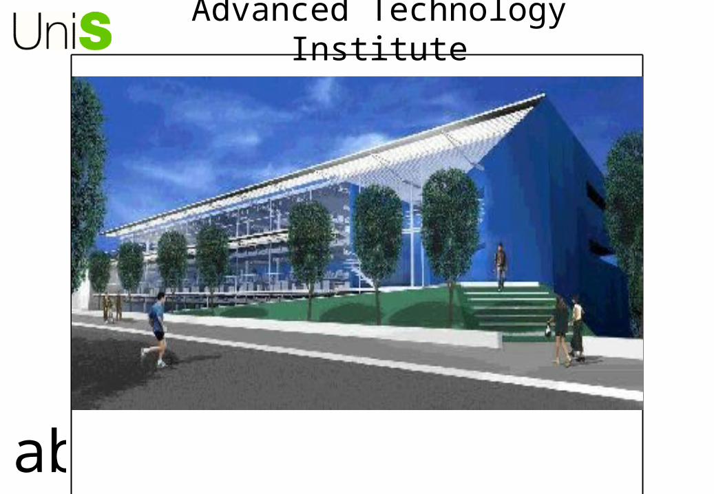
Advanced Technology Institute
abcdefghijklm
ATI: a £10m UniS/HEFCE 50:50 Joint Venture
For UniS
* Building on existing strengths while allowing for new initiatives
* A high-technology beacon at the campus entrance
* A research hotel for chosen industry
For HEFCE
* Joint Infrastructure Fund (JIF) support for state of the art projects
* Support of strategic research for future industry
* A strengthening of science that underpins biotechnology
RATIONALE:
* Co-locate six research groups from three Schools to stimulate cross-disciplinary research:
Microwave subsystems, lasers and optoelectronics, large area electronics, ion beam applications, high pressure, biosensors
* Rationalise the use of cleanroom facilities at UniS* Multi-purpose facility capable of rapid redirection of use. A new
concept in university research management
abcdefghijklm
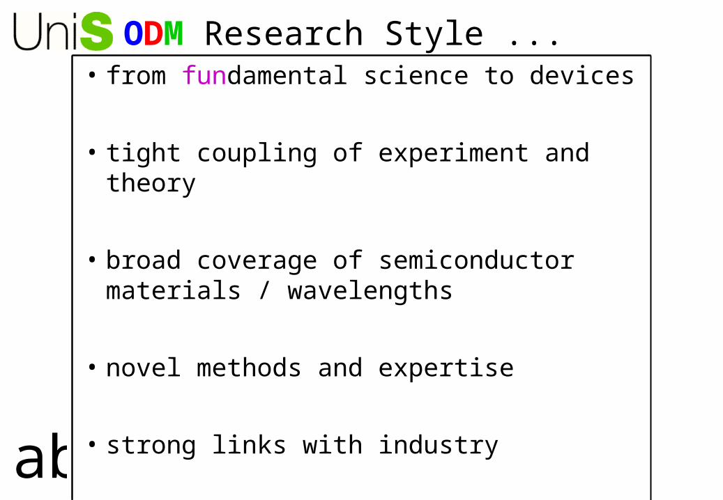
ODM Research Style ...• from fundamental science to devices
• tight coupling of experiment and theory
• broad coverage of semiconductor materials / wavelengths
• novel methods and expertise
• strong links with industry

abcdefghijklm
ODM … fundamental to applied
Fundamental
Applied
Fundamental interactions
Device character-
isation
Systems concepts
Systems character-
isation
Material properties
Device concepts
Device modelling
and optimisation
System modelling
and optimisation
Materialcharacter-
isation
ODM - Physics Department
collaboration with Electronic Engineering Dept and Industry

abcdefghijklm
new devicedesign
device character-
isation
ODM … theory AND experiment
wafer growth
test structure fabrication
advanced device fabrication
device modelling
material charact-erisation
basictheory
physical device
conceptbasic
experi-ments
material properties
device proof-of-principle
device fab.

abcdefghijklm
ODM … theory AND experimentexperimental
method
novel optical characterisation
hydrostatic pressure
light emission from lasers / LEDs
electrical characterisation
femtosecond measurements
theoretical method
strain distribution and wavefunctions
electronic structure calculations
gain calculation
Monte Carlo simulation
first-principle calculations
phenomena studied
growth & structure e.g. quantum dots
dependence on composition
optical gain / loss in semiconductor
electron transport
ultrafast phenomena

abcdefghijklm
ODM ... on your wavelength!
UV visible NIR MIR FIR MMW RFSpectral range:
Applic-ations:
optical storage
displays
opticalcomms
sensing
imaging radar
wireless
Experi-mental methods:
THz
FELUltrafast
electronics
tunable lasers / OPA
Novel materials/structures:
dilute nitrides:GaInNAs <-> GaInNSb
inter-subband devices:Quantum Cascade LD
GaN InGaAs Electronics:Si, SiGe
GaAs
Pb salts
InGaAsP HgCdTe
Materials for sources:

abcdefghijklm
ODM ... facilities and expertise
Experimental facilities
New ATI facilities
Theoretical methods
• application of hydrostatic pressure to optoelectronic devices and materials
• novel modulated reflectance methods • users of FELIX Free Electron Laser• wide range of standard methods:
optical, electronic, cryogenic
• bandstructures and transition rates of semiconductor nanostructures• mechanical-electronic-optical properties of strained semiconductors• novel ultrafast photon-electron interactions and transport
•new ultrafast laser facility•extensive clean room for fabrication
abcdefghijklm
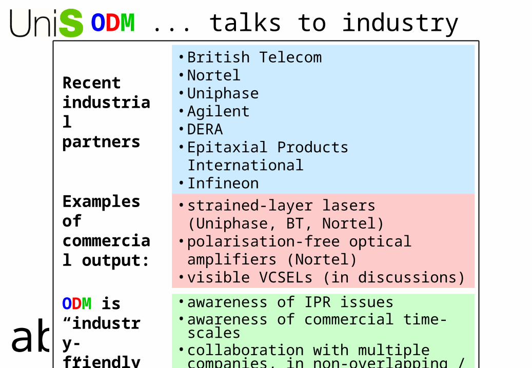
ODM ... talks to industry
Recent industrial partners
• awareness of IPR issues• awareness of commercial time-scales• collaboration with multiple companies, in
non-overlapping / non-competing projects
ODM is “industry-friendly”:
Examples of commercial output:
• strained-layer lasers (Uniphase, BT, Nortel)
• polarisation-free optical amplifiers (Nortel)• visible VCSELs (in discussions)
• British Telecom• Nortel• Uniphase• Agilent • DERA• Epitaxial Products International• Infineon

abcdefghijklm
ODM ... collaboration model
Industrial collaborator
wafer growth
teststructure fabrication
advanced device fabrication
device character-isation
new device design
device modelling
material character-isation basic
theory
physical device concept
UniS-ODM
Close collaboration of UniS-ODM with industry
tightly-coupled experiments
and modelling on real-world
devices