overview of emerging nanotechnology - jst · overview of emerging nanotechnology kazunobu tanaka...
TRANSCRIPT

Overview of Emerging Nanotechnology
Kazunobu Tanaka
Principal FellowCenter for Research and Development Strategy (CRDS)
Japan Science and Technology Agency (JST)
JST-DFG workshop on NanoelectronicsKarasuma Kyoto Hotel, Kyoto, 21-23 January 2009

Nanotechnology(Nanoscience and Nanotechnology)
- Definition- World-wide Public Funding- Evolution of Nanotechnology

Nanoscience & Nanotechnology(Nanotechnology)
Phenomena, Properties, Functions,Ability to measure, control, and manipulate matterIn a range of 1-100 nm : “Nano-world”(from atomic scale up to ~100 molecular diameter)
Enabling novel applications:Nanoelectronics, Nano-biotechnology,Nano-manufacturing, NEMS, and focus will beon Food, Water, Environment, Energy, Materials
World-wide public R&D funding started in 2001, initiated by NNI (USA),
and now roughly 30 countries have their own NNI’s

Courtesy: MC. Roco
Public R&D Funding to Nanotechnology
Rapid rise after 2001, and still keeps increasing

Nanoscience & Nanotechnologybefore and after the Year of 2001
What’s an essential difference between them?
R&D projects on nanoscience & nanotechnology from early 1980’s up to 2001 / A challenge to nano-worldwithin a framework of each independent discipline
National Nanotechnology Initiatives after 2001 /Integrative projects with huge R&D budget (Investment)Interdisciplinary collaboration is strongly encouraged inorder to create new frontiers of nanoscience & nano-technology towards “Innovation” (Funding Policy)
R&D Outcome ← Investment + Funding PolicyHow to promote interdisciplinary collaboration

Evolution of NanotechnologyFirst generation (~1990~) Independent Nano
Access to Nano-world (1-100nm) in each independent discipline; via top-down, bottom-up or combination
TEM, STM, ALE, lithography, CNT, supra-molecule
Second generation (~2000~) Fusion NanoInterdisciplinary fusion of Nano-worlds of different disciplines
low-k material via block-copolymer process,graphene on Si, DNA transistor, nano-DDS
Third generation (~2010~) Integration NanoIntegration of various Nano-worlds into functional sytems
molecular E, nano-bot, hierarchical self-assembly
Interdisciplinary fusion, Integration - Key issues

Courtesy: MC. Roco
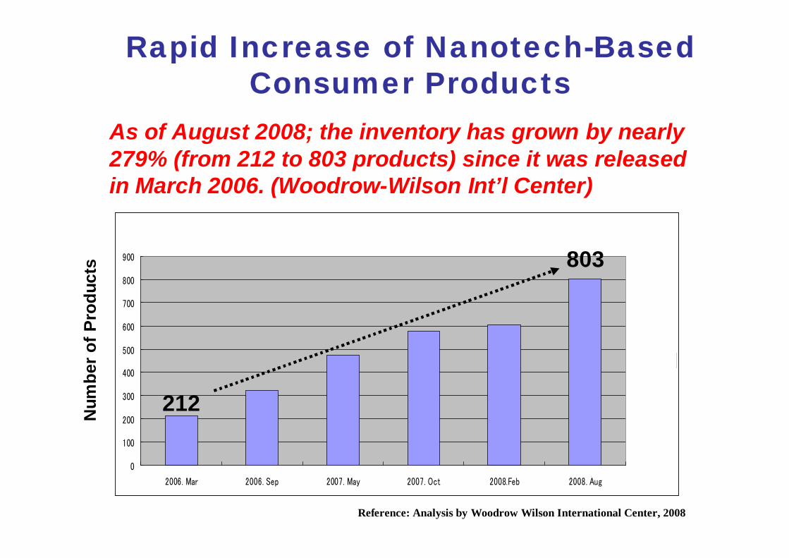
As of August 2008; the inventory has grown by nearly 279% (from 212 to 803 products) since it was released in March 2006. (Woodrow-Wilson Int’l Center)
Rapid Increase of Nanotech-Based Consumer Products
製品の数
0
100
200
300
400
500
600
700
800
900
2006. Mar 2006. Sep 2007. May 2007. Oct 2008.Feb 2008. Aug
製品の数
803
Reference: Analysis by Woodrow Wilson International Center, 2008
Num
ber o
f Pro
duct
s
212

Nanotechnology-based ProductsRapid increase after 2006
Nanotechnology-based goods in the worldPEN (W-W Int‘l Center, USA) 803 (Aug, 2008)
Practical Use of Nanotechnology in JapanSurveillance Study (JST-CRDS, Japan) 386 (Dec, 2007)
“Nanomark” commercial goods in Taiwan“Nanomark” system (2005,Taiwan) >100 (Jan, 2008)
World market prediction corrected – from US$1T to US$3.1T ( in 2015 )

Articles on the nanotechnology published in newspapers and magazines, etc. were retrieved, and classified into "Research stage", "Development stage", and "Practical use stage". Period covered: 2004-2007Retrieval object: Nikkei high technology, Nikkei Nano business, weekly nanotech, and Report of Funding (NEDO/JST)
130
39
60
32
Nano materials
1454105154133213276442Total
3863412234314194Practical use
58928395411394201D
47943103565741147R
TotalMeas./ Analysis
Medical / Biotech
Environ. / Energy
Indust.material
LifeElectronicsStage
Electronics
Daily Goods
Industrial material
Environment / Energy
Medical / Biotechnology
Measurement / Analysis
Nanomaterials
From the investigation at 2008.12 by JST_CRDS
Practical use of nanotechnology(2004 – 2007)
Total 386
Daily goods 141Electronics 94Indust. Materials 43
Practical Use of Nanotechnology in Japan

Status of Japan National R&D Program on
Nanotechnology / Materialas

Cabinet OfficeCouncil for S&T Policy
(CSTP)Minister of Statefor S&T Policy
MIC
Min
istry
of I
nter
nal
Aff
airs
and
C
omm
unic
atio
ns
MEX
TM
inis
try o
f Edu
catio
n C
ultu
re, S
ports
, S&
T
MH
LWM
inis
try o
f Hea
lth,
Labo
r and
Wel
fare
MA
FFM
inis
try o
f Agr
icul
ture
, Fo
rest
ry a
nd F
isher
ies
MET
IM
inis
try o
f Eco
nom
y,
Trad
e an
d In
dust
ry
MLI
TM
inis
try o
f La
nd,
Infr
astru
ctur
e an
d Tr
ansp
ort
MO
EM
inis
try o
f th
e En
viro
nmen
t
Promotion System of S&T Policy in Japan
Relevant ministries in S&T policy
Image: Office ofPrime Minister
JSPS
JST NEDO
Prime Minister
Courtesy: CSTP

Building an S&T Basic Plan towards the Future of Japan
●Increasing R&D budget
17 trillion yen (actual expenditure 17.6 trillion).
●Structuring a new R&D system
Support plan for post-doctoral fellows, etc.
●Increasing R&D budget
17 trillion yen (actual expenditure 17.6 trillion).
●Structuring a new R&D system
Support plan for post-doctoral fellows, etc.
●Key policies
-Prioritization of R&D on national/social subjects
-Doubling of competitive research fundsTotal budget : 24 trillion yen (actual expenditure 21.1 trillion)
●Key policies
-Prioritization of R&D on national/social subjects
-Doubling of competitive research fundsTotal budget : 24 trillion yen (actual expenditure 21.1 trillion)
●Key policies●Key policies1st Basic Plan
(FY 1996-2000)
3rd Basic Plan
(FY 2006-2010)
How to nurture creative S&T human resources?Further reform of S&T systems, leading to higher performance,Strategic prioritization of R&D themes.
2nd Basic Plan
(FY 2001-2005)
*Total budget target:25 trillion Yen(€210/$270 billion)roughly 1% of GDP
Courtesy: CSTP

Strategic priority setting in S&T
As for policy-mission oriented R&D4 priority promotion areas + 4 promotion areas were set up in the 2nd and 3rd S&T Basic Plans
4 priority promotion areas :Life scienceITEnvironment scienceNanotechnology and Materials (FY2001~)
The Second S&T Basic Plan (FY2001-2005)The Third S&T Basic Plan (FY2006-2010)

Public Funding forNanotechnology/Materials in Japan2nd S&T Basic Plan (FY2001 - FY2005)¥460B /5yrs3rd S&T Basic Plan (FY2006 - FY2010)¥76.2B /FY2006¥78.6B /FY2007¥86.5B /FY2008
NT&M shares 4~5% of total funding for 8 promotion areas (LS, IT, Env., NT&M, Energy, Mnf, Infra, Frtr)
Funding gradually increases since 2001, and will keep the level at least up to 2010

Progress in Nanoscience & Nanotechnology
(Japan – up to 2008)Materials
Strongly-correlated electrons system / Transparent Amorphous Oxide Semiconductor / TiO2 photocatalysis – Commercialization/ CNT – Super growth / Fe pnictide - Superconductor
Nano-biotechnology Cell sheet Engineering – Tissue Eng. without scaffolds / Drug Delivery System (DDS)
Nano-electronicsSi technology / More Moore, More than Moore, Beyond CMOSSpintronics – Tunneling Magneto Resistance / MRAM Organic Electronics – EL, transistor, Solar cellsMolecular Electronics?
Further progress ← Integration & Evolution ofNanoscience & Nanotechnology

Japan National R&D Program on Nanotechnology / Materials (1)
Observations mainly from activities up to 2005FY (2nd S&T BP)One of the top three countries highly contributing to Nanoscience & Nanotechnology publications and patents / Strongest in S&T of NanomaterialsTechnology Strategy Road Map (METI) Nanotechnology Business Road Map (NBCI)Internaitonal Nanotechnology Exhibition & ConferenceThe biggest scale in the world !But frustrated by slow technology-transfer of research output to new and existing industry “Excellent scientific outcome, but some frustration in tech-transfer to innovation” – International Advisory Committee for the evaluation of JST Basic Research Program (Jan 2006)
Policy makers complained of slow return of their investment although It takes time before any emerging technology drives real innovation

Japan National R&D Program on Nanotechnology / Materials (2)
The 3rd Science and Technology Basic Plan (2006-10FY) Nanotechnology / Materials - 10 Strategic S&T Priorities①Materials for reducing costs of clean Energy, ②Materials for replacing rare or deficit materials, ③Nanotech and Materials supporting security and safety, ④Materials for innovation, ⑤Electronics for Break-through Devices, ⑥Nano-biotechnology and Nano-medical Technology for very early diagnosis, ⑦R & D for the Social Acceptance of Nanotechnology, ⑧Advanced R & D at Innovation COE’s for commercialization of Nanotechnology, ⑨Nano-measurement and Nano-Processing technology, ⑩X-ray Free Electron Lasers
Inter-ministry Projects (CSTP)Nano-DDS, Medical use nano devices (2005 FY ~/ 2nd Basic Plan)Responsible R&D of Nanotechnology (2007FY~/ 3rd Basic Plan)
Inter-ministry CollaborationsMaterials Strategy for replacing Rare, Deficit or Toxic materials (METI / MEXT 2006FY~)Nanoelectronics (METI / MEXT 2007FY~)
Inter-ministry coordination – being improved

Japan National R&D Program on Nanotechnology / Materials (3)
Social Acceptance (Responsible R & D)Project “ Standardization of Nanoparticle Risk Evaluation Method ”2005-2007FY/ METI, AISTProject “Facilitation of Public Acceptance of Nanotechnology ”2005FY / MEXT, METI, MHLW, MOENEDO Project “Risk Assessment & Management of Manufactured Nanomaterials” 2006-2010FY / AIST , Univs , Industry / US$ 20MLate start, but running under strong inter-ministry collaborationCoordinated by CSTP
User Facilities NetworkNanotechnology Support Project (MEXT/2002-2006FY)14 Centers/open facilities/no charge system/US$2M/YEncouraging new SME’s to participate in NanotechnologyNot enough for accelerating interdisciplinary collaborationCharge system started in the second phase (2007~)
Social Acceptance, User Facilities – most important components, but funding is not enough
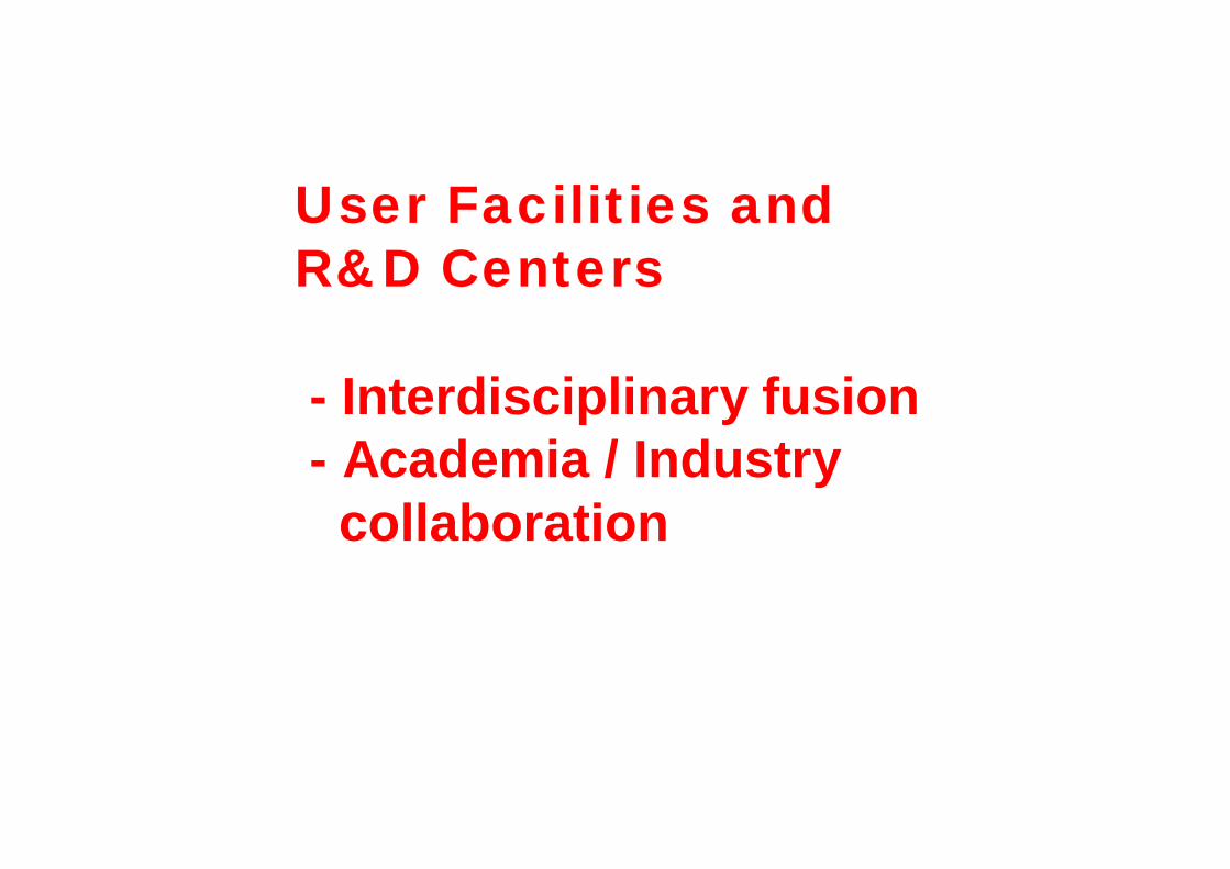
User Facilities and R&D Centers
- Interdisciplinary fusion- Academia / Industrycollaboration
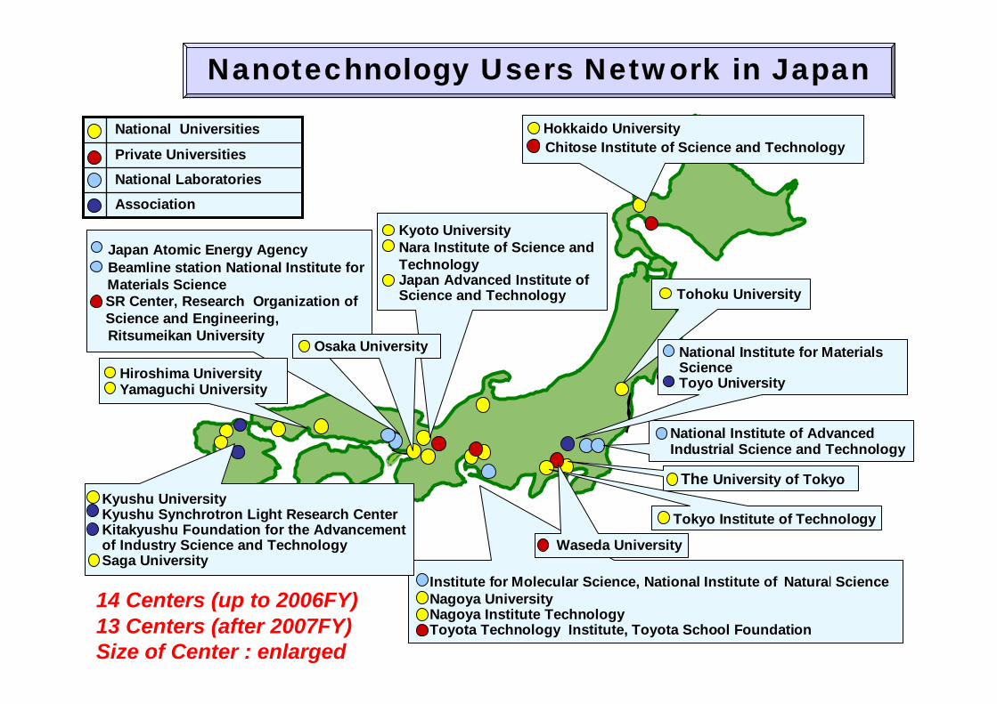
Institute for Molecular Science, National Institute of Natural ScienceNagoya UniversityNagoya Institute TechnologyToyota Technology Institute, Toyota School Foundation
Japan Atomic Energy AgencyBeamline station National Institute for Materials ScienceSR Center, Research Organization of Science and Engineering, Ritsumeikan University
Hiroshima UniversityYamaguchi University
The University of Tokyo
Association
National Laboratories
Private Universities
National Universities
Nanotechnology Users Network in Japan
Tohoku University
Kyoto University Nara Institute of Science andTechnologyJapan Advanced Institute of Science and Technology
National Institute of Advanced Industrial Science and Technology
Tokyo Institute of Technology
Waseda University
Hokkaido UniversityChitose Institute of Science and Technology
Osaka University
Kyushu UniversityKyushu Synchrotron Light Research CenterKitakyushu Foundation for the Advancementof Industry Science and TechnologySaga University
National Institute for Materials ScienceToyo University
14 Centers (up to 2006FY)13 Centers (after 2007FY)Size of Center : enlarged

韓国
Strategic Investment to Facilities / Accelerating Interdisciplinary CollaborationMulti-Funding System needed for Sustainable Operation of User Facilities
※Numbers in Table: Fraction(%) of total Revenue
(※USA, Japan: FY2001-2005, Korea: FY2001-2007, Taiwan: FY2003-2008)
米国 台湾 日本
Revenue of Nanotech. User Facilities
R&D77%
Social Dimension
8%Facilities
15%
R&D78%
Education6%Facilities
16%
1%Facilities19%
R&D80%
R&D97.5%
2.5%
Education Facilities
USA Korea Taiwan Japan
Countries Government(%)
Charging System (%)
Mat.Fund.From Reg. Gov. (%)
ConsortiumDonation (%)
USA(NNIN 13centers) 30 30Korea(KANC) 30 7 58 5UK(MNT Network) 50Japan(14centers) 100 - - -
40
50

Courtesy: MC. Roco

UC BerkeleyStanfordUCSBUCLA
Arizona State RiceTX A&M
UT DallasUT Austin
Notre DamePurdue
Pen State
Michigan
SUNY AlbanyHarvardMIT
YaleRPI
U of MD
WIN
INDEX
MINDNRI Funded Universities
SWANIndustry-Gov-AcademiaAllience (35 univs)
Four Institutes(21 states)
NRI Mission:Demonstrate novel “beyond CMOS”computing devices
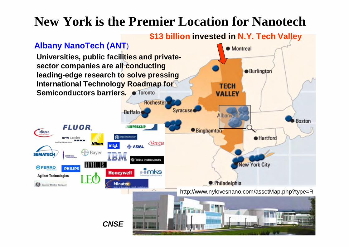
New York is the Premier Location for Nanotech
Albany NanoTech (ANT)Universities, public facilities and private-sector companies are all conducting leading-edge research to solve pressing International Technology Roadmap for Semiconductors barriers.
$13 billion invested in N.Y. Tech Valley
CNSE
http://www.nylovesnano.com/assetMap.php?type=R

Courtesy: R. DeKeersmaecker

Courtesy: R. DeKeersmaecker

Coutesy: MC. Roco
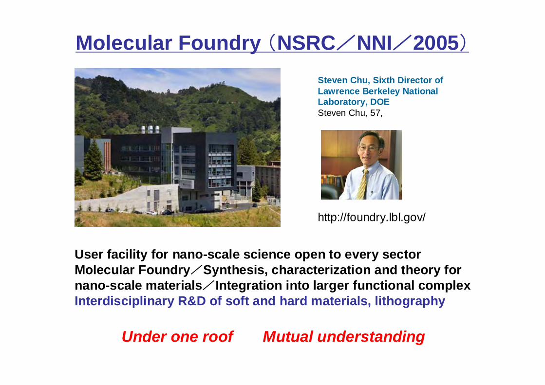
http://foundry.lbl.gov/
Steven Chu, Sixth Director of Lawrence Berkeley National Laboratory, DOESteven Chu, 57,
Molecular Foundry (NSRC/NNI/2005)
User facility for nano-scale science open to every sectorMolecular Foundry/Synthesis, characterization and theory for nano-scale materials/Integration into larger functional complexInterdisciplinary R&D of soft and hard materials, lithography
Under one roof Mutual understanding

Obama’s Remarkable Choice for Energy SecretaryThis is a signal Obama’s administration will “value science”. “We will make decisions based on the facts, and we understand that facts demand bold action,” Obama said.
Berkeley Lab Director Steven Chu shared the 1997 Nobel Prize in Physics for "development of methods to cool and trap atoms with laser light."
Steven Chu
http://wonkroom.thinkprogress.org/2008/12/10/steven-chu-new-energy/

Government funding projects
Next generation device project
2001 2002 2003 2004 2005 2006 2007 2008 2009 2010 2011 2012 2013 20
METI/NEDO MIRAI project
MEXT Si Nanoelectronics project
METI Nanoelectronics project
JST / MEXTWatanabe-CREST Project
Courtesy: H. Watanabe

✔ Next stage R&D programs,especially Nano-electronics, to be launched in 2010 by the new public-private framework, based on study with
industries, such as
COCN
✔ MEXT & METI’s joint initiative, working together with relevant universities &
industries and the Cabinet office,
CSTP
✔ Mutually beneficial Tie-Up with universities to be developed, cooperated
with MEXT, especially taking account of the
2 aspects bellow
(1) Human resource development of next generation with the most advanced nanotech knowledge & facilities
(2) Concentrated investment to the most advanced nanotech facilities with wide range of use by researchers ofpartnered labs
✔ International researchcooperation to be promoted, searching for innovative front edge
✔ International joint research on advanced Nano-electronics of 1M$ to be globally offered by AIST (2009 budget request)
Nanotech Research Competence in Tsukuba & New Framework of Public-Private Collaboration for Nanotech Driven Innovation
930 MHz NMR
Cluster of Research Labs of Naonotech Leading Companies
In TSUKUBA
National Institute forMaterials Science
National Institute of Advanced Industrial Science &Technology*
4500㎡(class 3) CR Gross area : 600m2
Nano-Processing Facility
Mitsubishi Chemical Group Science & Technology Research Center, Inc. Tsukuba Area
AstellasPharmaceutical Inc., Tsukuba (Miyukigaoka, Toukoudai)
Sumitomo Chemical Co., Ltd. Tsukuba Research Laboratory
KURARAY CO., LTD. Tsukuba Research Laboratories
Hitachi Chemical Co.,Ltd.TsukubaResearch Lab
ULVAC JAPAN, Ltd. Tsukuba Institute for Super Materials
JSR Corporation Tsukuba Research Laboratories
Texas Instruments Japan Tsukuba Technology Center (TRDC)
Intel K.K. Tsukuba
NEC Corporation Tsukuba Research Laboratories
UHV TEM
物質molecular
材料material
部材device/
component製品
product
Two 300m2 CRsand 100m2 CR
Power Electronics Research Center
✔ Research Association Law to be amended in 2009 to promote open-innovation type of R&D
consortium
✔ Nano-material safetyreseach program to be proposed in 2010 internationally by AIST, jointly worked with NBCIG
LOB A
L Link
ACADEMIC Link
✔ Essential Nonotech-facilities, such as SCR, to be renovated to highly energy efficient & all-around test device foundry, funded by METI (2009 budget request)
✔ Nano-tube joint R&D program to be proposed by AIST in 2010 as its core competence
- Japan's sole National Institute specializing in materials science, principally funded by MEXT (Ministry of Education, Culture, Sports, Science & Technology).
- All 450 researchers involved in various fields of materials science, based on the concept of “Nanotechnology-Driven Materials Science for Sustainability”.
- World's top level research facilities such as Ultra-High Voltage Electron Microscopes, High Magnetic Field (37.3 Tesla) and Solid-State NMR (930MHz).
- Top research organization in Japan as for the number of published papers on materials science per one researcher.
- Press on with globalization and fostering researchers as a world-leading research center.
- One of the Centers of Advanced Nanotechnology Network (NIMS Center for Nanotechnology Network)
- Japan's largest National Institute with 2400 researchers conducting research from the base to the application on various fields of industrial technology, principally funded by METI (Ministry of Economy , Trade & Industry).
- About 800 researchers involved in Nanotechnology driven field (Nano-electronics , Nano-photonics, Nano-materials etc.), based on the concept of “Integration for Innovation”.
- More than 10 clean rooms, such as the super clean room (SCR:4500m2) under Millennium Research for Advanced Information Technology (MIRAI) project, collaborated with the private consortium “Selete”and various clean rooms essential for a wide range of Nanotech-driven-research (Silicon, Inorganic and Organic Devices, MEMS etc.)
- One of the Centers of Advanced Nanotechnology Network (Nano-Processing Partnership Platform)
<Draft Concept>
Courtesy: R. Doi (METI)

SummaryNanotechnogyWorld-wide Investment (public and private) keepsincreasing from $9.5B (2005) up to $14.9B (2008)Nanotech-based goods – rapid increase after 2006
Now in the second generation (Fusion Nano)Towards the third generation (Integration Nano)
User Facilities and R&D Open Centers are cruciallyImportant for promoting and accelerating inter-disciplinary fusion and integration of various types ofnanoworlds developed independently.
Nano-electronicsIMEC, Albany, NRI, ・・・, New R&D center in Japan?
YES, WE CAN