overeenkomst - cordis.europa.eu ict large-scale integrating project deliverable d7.12 – part 1...
TRANSCRIPT
ICT-611439
TERASEL
Thermoplastically deformable circuits for embedded randomly shaped electronics
Instrument : Large-scale integrating project (IP) Thematic Priority : Information and Communication Technologies (ICT)
Deliverable D7.12
Final Report
Part 1 : Final publishable summary
Due date of deliverable : 30.9.2016
Actual submission date : 25.11.2016
Start date of Project : 1.10.2013 Duration : 36 months
Responsible Beneficiary : imec Revision : 2.0 Contributing Beneficiaries : All Contact person : Jan Vanfleteren – imec
Project co-funded by the European Commission within the Seventh Framework Programme (2007-2013)
Dissemination Level
PU Public X
PP Restricted to other programme participants (including the Commission Services
RE Restricted to a group specified by the consortium (including the Commission Services)
CO Confidential, only for members of the consortium (including the Commission Services)
TERASEL ICT Large-scale integrating project Deliverable D7.12 – Part 1
ICT-611439 - 1/70 - 25.11.2016
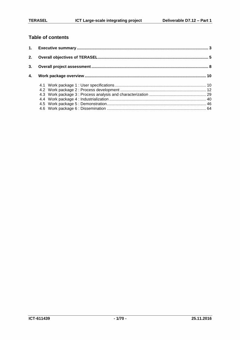
Table of contents 1. Executive summary ...................................................................................................................... 3 2. Overall objectives of TERASEL ................................................................................................... 5 3. Overall project assessment ......................................................................................................... 8 4. Work package overview ............................................................................................................. 10
4.1 Work package 1 : User specifications .................................................................................. 10 4.2 Work package 2 : Process development ............................................................................. 12 4.3 Work package 3 : Process analysis and characterization ................................................... 29 4.4 Work package 4 : Industrialization ....................................................................................... 40 4.5 Work package 5 : Demonstration ......................................................................................... 46 4.6 Work package 6 : Dissemination ......................................................................................... 64
TERASEL ICT Large-scale integrating project Deliverable D7.12 – Part 1
ICT-611439 - 2/70 - 25.11.2016
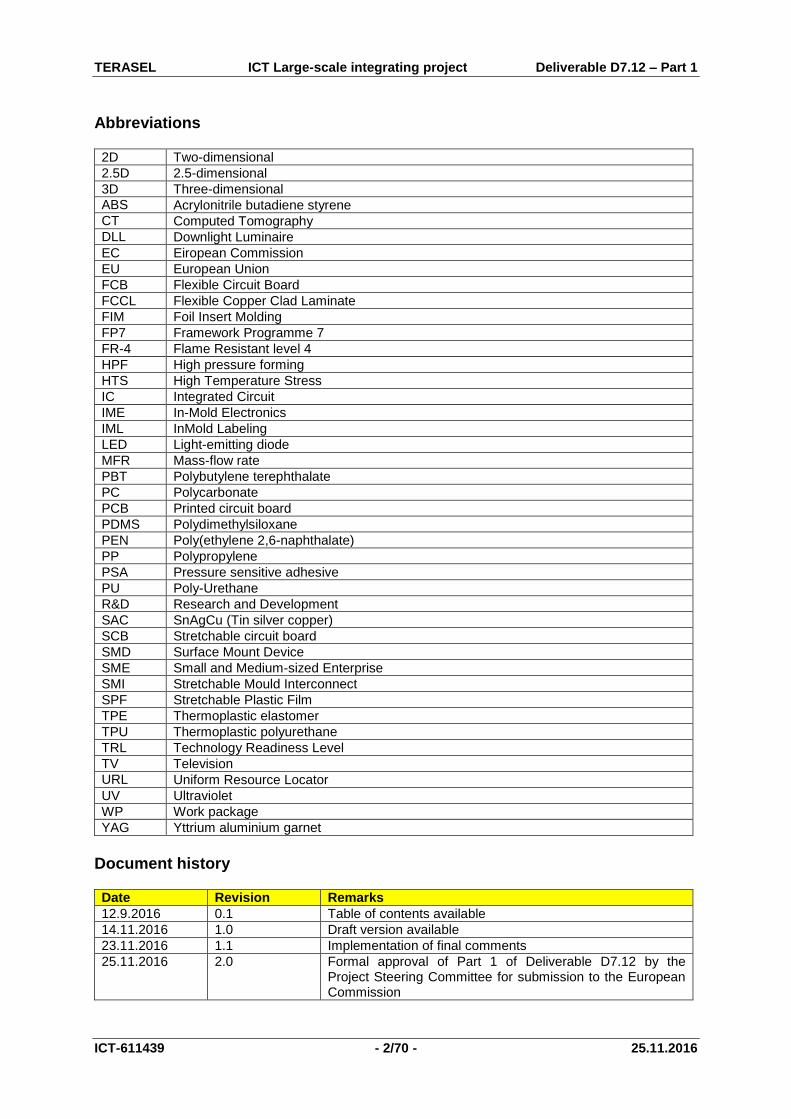
Abbreviations 2D Two-dimensional
2.5D 2.5-dimensional
3D Three-dimensional
ABS Acrylonitrile butadiene styrene
CT Computed Tomography
DLL Downlight Luminaire
EC Eiropean Commission
EU European Union
FCB Flexible Circuit Board
FCCL Flexible Copper Clad Laminate
FIM Foil Insert Molding
FP7 Framework Programme 7
FR-4 Flame Resistant level 4
HPF High pressure forming
HTS High Temperature Stress
IC Integrated Circuit
IME In-Mold Electronics
IML InMold Labeling
LED Light-emitting diode
MFR Mass-flow rate
PBT Polybutylene terephthalate
PC Polycarbonate
PCB Printed circuit board
PDMS Polydimethylsiloxane
PEN Poly(ethylene 2,6-naphthalate)
PP Polypropylene
PSA Pressure sensitive adhesive
PU Poly-Urethane
R&D Research and Development
SAC SnAgCu (Tin silver copper)
SCB Stretchable circuit board
SMD Surface Mount Device
SME Small and Medium-sized Enterprise
SMI Stretchable Mould Interconnect
SPF Stretchable Plastic Film
TPE Thermoplastic elastomer
TPU Thermoplastic polyurethane
TRL Technology Readiness Level
TV Television
URL Uniform Resource Locator
UV Ultraviolet
WP Work package
YAG Yttrium aluminium garnet
Document history Date Revision Remarks
12.9.2016 0.1 Table of contents available
14.11.2016 1.0 Draft version available
23.11.2016 1.1 Implementation of final comments
25.11.2016 2.0 Formal approval of Part 1 of Deliverable D7.12 by the Project Steering Committee for submission to the European Commission
TERASEL ICT Large-scale integrating project Deliverable D7.12 – Part 1
ICT-611439 - 3/70 - 25.11.2016
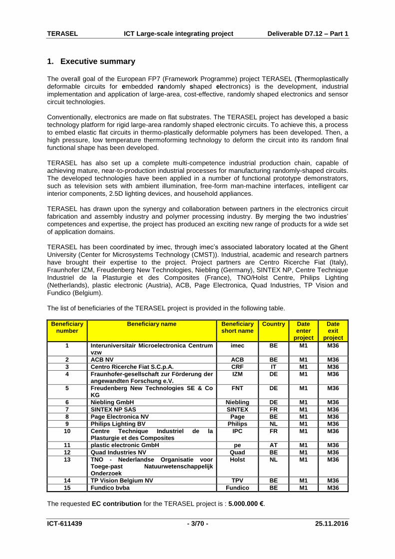
1. Executive summary The overall goal of the European FP7 (Framework Programme) project TERASEL (Thermoplastically deformable circuits for embedded randomly shaped electronics) is the development, industrial implementation and application of large-area, cost-effective, randomly shaped electronics and sensor circuit technologies. Conventionally, electronics are made on flat substrates. The TERASEL project has developed a basic technology platform for rigid large-area randomly shaped electronic circuits. To achieve this, a process to embed elastic flat circuits in thermo-plastically deformable polymers has been developed. Then, a high pressure, low temperature thermoforming technology to deform the circuit into its random final functional shape has been developed. TERASEL has also set up a complete multi-competence industrial production chain, capable of achieving mature, near-to-production industrial processes for manufacturing randomly-shaped circuits. The developed technologies have been applied in a number of functional prototype demonstrators, such as television sets with ambient illumination, free-form man-machine interfaces, intelligent car interior components, 2.5D lighting devices, and household appliances. TERASEL has drawn upon the synergy and collaboration between partners in the electronics circuit fabrication and assembly industry and polymer processing industry. By merging the two industries’ competences and expertise, the project has produced an exciting new range of products for a wide set of application domains. TERASEL has been coordinated by imec, through imec’s associated laboratory located at the Ghent University (Center for Microsystems Technology (CMST)). Industrial, academic and research partners have brought their expertise to the project. Project partners are Centro Ricerche Fiat (Italy), Fraunhofer IZM, Freudenberg New Technologies, Niebling (Germany), SINTEX NP, Centre Technique Industriel de la Plasturgie et des Composites (France), TNO/Holst Centre, Philips Lighting (Netherlands), plastic electronic (Austria), ACB, Page Electronica, Quad Industries, TP Vision and Fundico (Belgium). The list of beneficiaries of the TERASEL project is provided in the following table.
Beneficiary number
Beneficiary name Beneficiary short name
Country Date enter
project
Date exit
project
1 Interuniversitair Microelectronica Centrum vzw
imec BE M1 M36
2 ACB NV ACB BE M1 M36
3 Centro Ricerche Fiat S.C.p.A. CRF IT M1 M36
4 Fraunhofer-gesellschaft zur Förderung der angewandten Forschung e.V.
IZM DE M1 M36
5 Freudenberg New Technologies SE & Co KG
FNT DE M1 M36
6 Niebling GmbH Niebling DE M1 M36
7 SINTEX NP SAS SINTEX FR M1 M36
8 Page Electronica NV Page BE M1 M36
9 Philips Lighting BV Philips NL M1 M36
10 Centre Technique Industriel de la Plasturgie et des Composites
IPC FR M1 M36
11 plastic electronic GmbH pe AT M1 M36
12 Quad Industries NV Quad BE M1 M36
13 TNO - Nederlandse Organisatie voor Toege-past Natuurwetenschappelijk Onderzoek
Holst NL M1 M36
14 TP Vision Belgium NV TPV BE M1 M36
15 Fundico bvba Fundico BE M1 M36
The requested EC contribution for the TERASEL project is : 5.000.000 €.
TERASEL ICT Large-scale integrating project Deliverable D7.12 – Part 1
ICT-611439 - 4/70 - 25.11.2016
The TERASEL project website address is : www.terasel.eu The project has been launched on October 1, 2013 for a duration of 36 months. The Project Coordinator and contact person for the TERASEL project is : Prof. Dr. Jan Vanfleteren Imec - Interuniversitair Microelectronica Centrum vzw Technologiepark 15 – Building iGent B-9052 Zwijnaarde Belgium Tel : +32-9-264.53.60 E-mail : [email protected]
TERASEL ICT Large-scale integrating project Deliverable D7.12 – Part 1
ICT-611439 - 5/70 - 25.11.2016
2. Overall objectives of TERASEL
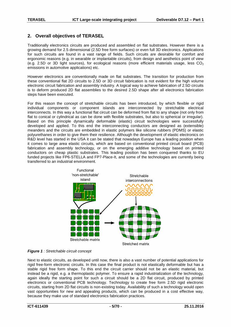
Traditionally electronics circuits are produced and assembled on flat substrates. However there is a growing demand for 2.5 dimensional (2.5D free form surfaces) or even full 3D electronics. Applications for such circuits are found in a vast range of fields. Such circuits are desirable for comfort and ergonomic reasons (e.g. in wearable or implantable circuits), from design and aesthetics point of view (e.g. 2.5D or 3D light sources), for ecological reasons (more efficient materials usage, less CO2 emissions in automotive applications) etc. However electronics are conventionally made on flat substrates. The transition for production from these conventional flat 2D circuits to 2.5D or 3D circuit fabrication is not evident for the high volume electronic circuit fabrication and assembly industry. A logical way to achieve fabrication of 2.5D circuits is to deform produced 2D flat assemblies to the desired 2.5D shape after all electronics fabrication steps have been executed. For this reason the concept of stretchable circuits has been introduced, by which flexible or rigid individual components or component islands are interconnected by stretchable electrical interconnects. In this way a functional flat circuit can be deformed from flat to any shape (not only from flat to conical or cylindrical as can be done with flexible substrates, but also to spherical or irregular). Based on this principle dynamically deformable (elastic) circuit technologies were successfully developed and applied. To this end the interconnecting conductors are designed as (extensible) meanders and the circuits are embedded in elastic polymers like silicone rubbers (PDMS) or elastic polyurethanes in order to give them their resilience. Although the development of elastic electronics on R&D level has started in the USA it can be stated that nowadays Europe has a leading position when it comes to large area elastic circuits, which are based on conventional printed circuit board (PCB) fabrication and assembly technology, or on the emerging additive technology based on printed conductors on cheap plastic substrates. This leading position has been conquered thanks to EU funded projects like FP6-STELLA and FP7-Place-It, and some of the technologies are currently being transferred to an industrial environment.
Figure 1 : Stretchable circuit concept Next to elastic circuits, as developed until now, there is also a vast number of potential applications for rigid free-form electronic circuits. In this case the final product is not elastically deformable but has a stable rigid free form shape. To this end the circuit carrier should not be an elastic material, but instead be a rigid, e.g. a thermoplastic polymer. To ensure a rapid industrialization of the technology, again ideally the starting point for such a circuit should be a 2D flat circuit, produced by printed electronics or conventional PCB technology. Technology to create free form 2.5D rigid electronic circuits, starting from 2D flat circuits is non-existing today. Availability of such a technology would open vast opportunities for new and appealing products, which can be produced in a cost effective way, because they make use of standard electronics fabrication practices.
TERASEL ICT Large-scale integrating project Deliverable D7.12 – Part 1
ICT-611439 - 6/70 - 25.11.2016
This leads us to the formulation of the core objective of the TERASEL project The EU research institutes and companies, leading the worldwide technology developments and industrialisation efforts on large area elastic circuits have taken full advantage of this leading position to tackle the challenge of developing, applying and industrializing the technology for 1-time, thermoplastically deformable circuits. To this end an equally important participation of research institutes and production companies from the polymer processing sector is necessary and, hence, also leading research and industrial knowledge centres from this field are partners in TERASEL. This multidisciplinary consortium has developed different processes for 1-time deformable circuits, based on 3 different elastic circuits technologies, which are close to additive printing and PCB technology technologies. In a simplified way of representation these processes consist of following principle steps:
Circuit design
2D manufacturing on a flat substrate of the electronic / sensor circuit and assembly of the components
Application of the polymer, thus encapsulating the circuit, and deformation of the embedded flat circuit and the polymer encapsulant from its initial 2D shape to the final 2.5D free form shape
Testing and use of the obtained 2.5D rigid free form circuit. Because the TERASEL project has such a strong starting point with its knowledge on elastic circuits, the partners believe that the necessary technology and processes can be developed in a reasonably short time (1.5 to 2 years). Therefore the consortium was confident that in this 3 year project it would be feasible to set up a complete production chain of industrial design, fabrication and application steps for free form rigid circuits by the end of the project. A key objective of TERASEL therefore is to establish this value chain, which would consist uniquely of TERASEL project partners. This production chain should allow a rapid scaling up to volume production. Nevertheless the established technology platform has also allowed the transfer of the developed technologies to partners, external to TERASEL, who might then become a link in the value chain. In TERASEL the developed technologies has been demonstrated in 5 applications of various fields :
Automotive (Centro Ricerche Fiat)
Lighting (Philips Lighting)
Consumer : Ambilight Television (TP Vision)
Ergonomic man-machine interface (Quad Industries)
Consumer : Household appliance (plastic electronic) Many more applications can be envisaged. Furthermore, the different partners in the consortium cover all necessary competences in electronics circuit fabrication and polymer processing, on an R&D level, as well as on industrial scale. TERASEL has 4 research partners, 5 large industrial entities and 6 SME’s, in total 15 partners from 6 different EU countries. Figure 2 lists the partners, their competences and their position in the production chain.

TERASEL ICT Large-scale integrating project Deliverable D7.12 – Part 1
ICT-611439 - 7/70 - 25.11.2016
Figure 2 : Listing of the partners with their competences and position in the production chain. This aim to develop processes and strongly work towards industrialisation is perfectly anticipating to one of the “key novelties” which will be introduced in the Horizon 2020 Framework Programme. Indeed these key novelties will include “more support for innovation and activities close to the market, leading to a direct economic stimulus”. This is exactly the aim of TERASEL, which thus could be considered as a forerunner project for the current Horizon 2020 Framework Programme.
TERASEL ICT Large-scale integrating project Deliverable D7.12 – Part 1
ICT-611439 - 8/70 - 25.11.2016
3. Overall project assessment Research in the domain of stretchable electronics has been going on since about 15 years now. Nearly all developments concentrate on dynamically deformable, i.e. elastic circuits. Even today a vast number of research activities is going on, resulting in new materials like intrinsically stretchable conductors, insulators, semiconductors, use of materials like hydrogels in soft electronics, novel devices like stretchable thin-film transistors, pressure and strain sensors, etc. However, when it comes to industrialisation and commercialisation one issue which consistently comes up, concerns the integration of these materials and novel components in larger systems. The interconnections of these components, and more in particular the interface between soft components and rigid standard electronics, which is always necessary to build a functional system, is the key weak point in the system when it comes to mechanical reliablility and durability of the product. Many of the groups, involved in TERASEL, also have a strong track record in the development of dynamically stretchable circuits. Thanks to the support of former projects like FP6-STELLA and FP7-Place-It, it can be stated that these groups are in the forefront when it comes to the development and application of elastic circuit technologies, which have the potential for being transferred to an industrial environment. Until now, however, these research projects have not led to wide industrial activity or products on the market, although decent reliability for the technologies was demonstrated. One exception is the USA based company MC10, which recently launched a smart patch, which has a limited stretchability, but it remains to be seen if this will be a commercial success. One reason for this very limited market uptake is that there is still a lack of confidence by producers and customers in the technology. When using electronic products which are exposed to continuous deformation, chances for defects due to misuse, like e.g. extreme bending or overstretching remain high. Product developers do not want to take the risk of the perception by the customer of delivering low quality products. For this reasons we believe that TERASEL is in a much better position as far as potential industrialisation of the technology is concerned. Although still the same technological principles as for dynamically stretchable circuits are used (stretchability by meander shaping of the conductors, production of the circuits on flat carriers, use of components-off-the-shelf (COTS), component assembly by established technologies (soldering or use of conductive adhesives,...) now the carrier is not an elastic polymer anymore, but instead rigid thermoplastic materials are used. The consequence is that after production the electronics are completely integrated in a rigid free-form plastic carrier, and thus retain their shape, without the components or connections being exposed to continuous stress due to shape changes of the smart object. The plastic carrier protects the embedded circuit and contributes to the robustness of the product. In the sections below the reader will find an extensive description of the activities which were deployed in the frame of 3 years of TERASEL. It is clear that these activities include the generation of technology and user specifications, basic technology development and technology demonstration, i.e. the type of activities which can be found in most of the other EC funded or other collaborative projects of this type. What makes TERASEL a special FP7 project is the fact that also a considerable amount of activities were directed towards the industrialisation of the developed technologies and demonstrators. This was included in the workplan precisely because we strongly believe in the high potential for industrialisation, because of the argumentation, outlined above. The aim of the project was to create industrial value chains, which in future would be able to produce smart plastic objects in moderate or large volumes. Therefore, all necessary competences were gathered in the consortium : end-users, partners from electronics manufacturing industry and from polymer processing industry, supported by the necessary specialised R&D institutes. When looking back at the project it can be stated that we succeeded not only in developing the necessary basic technologies with the required reliability properties, and apply these technologies in a number (5) of demonstrators, but moreover we succeeded in setting up the industrial production chains, capable to produce these demonstrators in reasonable quantities. The status at the end of the project concerning potential industrialisation was quantified in terms of TRL levels, and it was concluded that TERASEL allowed us to increase the TRL level with 2 units (from level 3-4 to level 5-6). This means that some issues remain before actual production can start, but we succeeded in realising considerable progress to such an industrialisation, and further steps to be taken are clear and to our mind deliverable. The will and enthousiasm to proceed on the road to industrial production of smart plastic objects is substantiated by participation of TERASEL partners in a number of follow-up

TERASEL ICT Large-scale integrating project Deliverable D7.12 – Part 1
ICT-611439 - 9/70 - 25.11.2016
projects (e.g. part of the granted H2020-InSCOPE project, with participation of Philips Lighting, TNO and imec, or a Flemish Community funded project with participation of ACB and IMEC in a different field of application, which cannot be disclosed here). From our contacts and dissemination activities it is indeed clear that besides the applications, served in TERASEL, many other can benefit from the TERASEL technologies to create new products and services. We strongly believe that TERASEL is only the start and the initiator project for delivering practicable technologies for the creation of smart plastic objects which will find their way to the market in this IoT era.

TERASEL ICT Large-scale integrating project Deliverable D7.12 – Part 1
ICT-611439 - 10/70 - 25.11.2016
4. Work package overview
4.1 Work package 1 : User specifications A. Work package objectives The objectives of Work package 1 of TERASEL are to understand the requirements of various actors based on a selection of use cases and applications of one-time deformable electronics, to gain insight in the different processes and to converge to process concepts to be investigated in the further work packages of the project. WP1 as such laid the foundation and set the proper direction to the development of the process technologies. WP1 is divided in 2 tasks, the first related to the requirements set by the end-users, the second related to the determination of production flow chain for 1-time deformable circuits.
B. Major achievements 1. User specifications The objective of this first task was the identification of the main specifications for the targeted demonstrators as well as the definition of components and processes for final development. The end-users’ specifications have been identified in terms of functionality, non-functional requirements, and design constraints including:
Targeted applications
Manufacturing process parameters
Materials: Plastic foils, inks, resins, adhesives
Required electronics components The five demonstrators are composed by functional plastic sheets embedded within the plastic component. This requires identification and investigation of the relevant manufacturing processes and specifications. The substrate technologies have been developed in WP2 (Process development) and WP3 (Process analysis and characterization) in order to match these specifications.
2. Process concept definition The overall scientific and technological aim of TERASEL was the development of large area randomly shaped electronics and sensor circuits, starting from flat circuits, which are fabricated and assembled using technologies from mainstream printed circuit board (PCB) manufacturing and electronics assembly industry. The process flow for such a circuit consists of following key steps:
Production of the circuit and assembly of the components using standard PCB and flex foil production facilities (but with adjusted parameters), i.e. after this step the circuit has a flat format, because standard electronic circuits are always produced and assembled in this way.
Application, already during the flat circuit production of previous step 1, and/or after finishing step 1, of a polymer which will serve as the carrier / embedding material of the circuit and which will allow a 1-time thermoplastic deformation of the circuit.
Deformation by thermoforming of the flat, polymer embedded circuit, from flat towards its final, free-form shape.
A representation of the process flow is shown in Figure 3.

TERASEL ICT Large-scale integrating project Deliverable D7.12 – Part 1
ICT-611439 - 11/70 - 25.11.2016
Electronic components embedded between polymer sheets
Stretched electronic circuit
Still functioning electronic components
Thermoformed polymer sheet
Forming b
Figure 3 : Process flow for turning a flat electronic circuit into a 3D electronic circuit by a forming process It is clear that electronic components and sensors cannot be deformed (in most of the cases not even bent), therefore the key feature for randomly shaped electronics is 1-time stretchable electrical interconnections, which connect the rigid components / component islands. When stretched they will maintain their electrical interconnection function, and therefore after deformation the circuit will keep its functionality, which it had in the flat state. In TERASEL, 3 versions for randomly-shaped electronics were developed and compared in terms of performance, cost, and potential for industrialization:
A first high density version, based on the use of polyimide foil, Cu stretchable conductors, SnAgCu solder assembly, and the use of a high T temporary carrier for the production of the circuit. This version is based on imec’s SMI (stretchable mould interconnect) technology for elastic circuits.
A second high density version, based on the use of laminated Cu on poly-urethane (PU) carrier foil and low T solder or adhesive component assembly. This version is based on FhG-IZM/FNT’s SCB (stretchable circuit board) technology for elastic circuits.
A third version which is a cost-effective version, based on the use of cheap plastic foil, Ag ink printed conductors and adhesive assembly of the components. This version is based on Holst’s SPF (stretchable plastic foil) based technology for elastic circuits.
In the sections that follow, for these 3 technologies the process concept descriptions for lab scale and industrial scale application are given.
Figure 4 : A thermoformed and overmoulded part realized in the 3 different technologies: SMI Technology, SCB Technology and SPF Technology
In the following sections, more insights are given in the technological details of the different technologies.

TERASEL ICT Large-scale integrating project Deliverable D7.12 – Part 1
ICT-611439 - 12/70 - 25.11.2016
4.2 Work package 2 : Process development A. Work package objectives The technologies for deformable electronics are based on the methodologies used for the fabrication of stretchable electronics. Three different approaches for stretchable electronics were employed: the SMI, the SCB and the SPF technology. The stretchability of the realized products is implemented through stretchable conductors between commercial (rigid) electronic components. Typical stretchable electronics target at high elasticity and softness – typcial use cases are medical, wearable, and textile electronics – while TERASEL aims at rigid three-dimensional freeform devices with integrated electronics. Thus the methodologies (design rules, fabrication approaches) developed for stretchable devices had to be modified in order to display rigidity, while being extendible at least once in a forming process. The requested rigidity was implemented by thermoplastic carrier panels, on which stretchable circuitries were directly build-up, or into which prefabricated stretchable system were integrated. The electronic systems realized in this way are thus stretchable electronics (by design) embedded into or attached onto a thermoplastic matrix. The fabrication for the circuitry and assembly of components are throughout done in panel level processing approaches. Subsequent to the fabrication, the functional systems were subjected to thermoplastic, high pressure forming processes and/or overmolding with additional polymers in order to shape the devices into its final three dimensional form. In Work package 2 the complete process chain for three dimensional formable systems was developed.
B. Major achievements 1. Circuit fabrication a. SMI technology The one-time deformable SMI process, graphically represented in Figure 5, starts with the production of carrier boards. The prevalent choice for substrate is 1.5 mm FR-4 glass-reinforced epoxy laminate, being both readily available at every PCB manufacturer and compatible with all the processing steps. The reusable pressure sensitive adhesive (PSA) comes in the form of a double sided tape, Taconic FH20LB TacSil tape, which is applied to the FR-4 using a hot roll laminator at 120°C as shown in step (b) of Figure 5. The boards are afterwards stacked in a vacuum press for one hour at 200°C and 2 MPa, and pre-baked in a vapour phase reflow oven using a default profile for SAC305 reflow soldering. These steps remove any moisture from the carrier board, and cause existing air bubbles to expand ahead of time. The flexible circuit board (FCB) which forms the basis for the SMI technology is fabricated using the default PCB processing steps without carrier board, as shown in step (d) of Figure 5. Typically UBE UPISEL SR-1220 flexible copper clad laminate (FCCL) is used with 50 µm of polyimide and 18 µm of copper, but a large variety of laminates were tested so far. This FCB is rolled onto the carrier board with counter traction to avoid wrinkling, resulting in a board as presented in step (e) of Figure 5. The next step (f) defines the stretchable interconnect support outline – the islands and meanders – by cutting the polyimide using a conventional depaneling laser. By tuning the laser ablation parameters it is possible to cut the FCB without damaging the PSA. Preference exists for picosecond pulse length UV Nd:YAG lasers as these leave less debris, which can negatively affect the PSA’s adhesive strength. On commercially available systems the spacing between the copper and the circuit outline should exceed 100 µm, making the minimum interconnect width ± 250 µm. The residuals not part of the circuit are then peeled away from the carrier, leaving behind the desired circuit (step g). Assembly is done using the proven method of stencil printing, pick-and-place assembly, and finally reflow soldering resulting in an assembled circuit as shown in step (h) of Figure 5. No-clean flux is advised as other types might negatively affect the long term performance of the device.

TERASEL ICT Large-scale integrating project Deliverable D7.12 – Part 1
ICT-611439 - 13/70 - 25.11.2016
Figure 5 : Stretchable Mould Interconnect (SMI) process flow for one-time deformable electronics. (a) Blank FR-4 board is cut to size. (b) Pressure sensitive adhesive is applied to FR-4 board. (c) Polyimide flexible copper clad laminate (FCCL) is cut to size. (d) The copper layer of the FCCL is etched into the desired pattern, resulting in the flex foil. (e) The flex foil is attached to the carrier made in step b. (f) The outline of the meanders and islands is cut into the flex foil without damaging the pressure sensitive adhesive. (g) The residual areas are peeled away. (h) Components are placed and assembled using reflow soldering. (i) A top layer of thermoplastic material is laminated onto the circuit. (j) The thermoplastic material is released from the carrier together with the circuit. (k) Additional layers are added to the laminate. The circuit is transferred into the thermoplastic laminate using lamination, as shown in step (i) of Figure 5. A thermoplastic elastomer (TPE) such as thermoplastic polyurethane (TPU) acts as an adhesive layer for the laminate and conforms to the circuit profile. At the same time the adhesion between most TPEs and the silicone based PSA is limited, allowing the TPE film to selectively remove the circuit from the carrier board without damaging either of them, resulting in the laminate shown in step (j) of Figure 5. Because the used TPE layers are very thin (± 100 µm) an additional rigid thermoplastic sheet (e.g. polycarbonate) is added on top. This sheet provides holes allowing some of the components to fit through, while others stay covered. To avoid damage to the components during lamination a suitable press pad needs to be added to the press book. Conventional multi-layer flex-rigid press pads were deemed unsuitable, leading to the use of Rogers BISCO Foam HT-870 as press pad. The resulting press book, illustrated in Figure 6, is able to conform to height differences in excess of 1 mm and is able to deal with pressure sensitive components such as zero insertion force (ZIF)
TERASEL ICT Large-scale integrating project Deliverable D7.12 – Part 1
ICT-611439 - 14/70 - 25.11.2016
connectors. Using the correct materials the thermoplastic laminate, now containing the circuit, debonds itself from the carrier board post-lamination. This laminate can then be built up further using lamination and over-moulding steps, resulting in the final laminate presented in step (k) of Figure 5. Symmetric laminates are recommended as this often places the circuit along the neutral stress line.
Figure 6 : Press book used for first-stage lamination of Stretchable Moulded Interconnect laminates. Finally the laminate is vacuum formed using the aforementioned processes. A key difference here with normal processing is the importance of sheet alignment. Failure to align the sheet properly will lead to component misplacement on the final 3D-shape, and might affect the functionality of the device. If a large component ends up in an area with a small bending radius the component can break, or at the very least excessive strain will be applied on the solder joint leading to device failure. For this a system with alignment pins and markers can be implemented on the machine’s clamping frame with relatively minor effort. The alignment pins should be kept away from the inside edge of the clamping frame, as this can lead to tears in the laminate during forming which causes vacuum leaks and badly formed parts as a result. In Figure 7, the parallel meander testvehicle is shown which was realized using the SMI technology.
Figure 7 : Parallel meander test vehicle before and after forming.
TERASEL ICT Large-scale integrating project Deliverable D7.12 – Part 1
ICT-611439 - 15/70 - 25.11.2016
b. SCB technology In the SCB (stretchable circuit board) technology the circuitry is build up using thermoplastic polyurethane as a carrier matrix. Typically the thickness of that matrix is around 200 µm. It contains wavy or meandering copper interconnector between electronic components. Electronic components are either grouped in areas were stretchability of the final system is inhibited or they are distributed over the device area. At the locations where components are assembled the polyurethane matrix has a window opened in order to access the copper structures. In order to be compatible with the reflow soldering of components a solder mask is applied and structured over the copper. As described in the section component assembly SnBi is used as a low temperature solder for reflow assembly of components. The fabrication of an SCB substrate is depicted in Figure 8. The sequence is (1.) Lamination of a copper foil (35 µm thick) onto a polyurethane sheet (100 µm thick), followed by (2.) photolithographic structuring of the copper sheet, (3. and 4.) application and structuring of a solder mask, (5.) lamination of a second (pre-cut) polyurethane sheet (again 100 µm) in order to embed the Cu tracks, (6.) finally a surface finish is applied on the copper pads. Throughout processing the substrate is fixed onto a temporary rigid carrier board. The build-up is fully compatible with printed circuit board fabrication procedures and chemistry.
Figure 8 : schematic representation of the SCB fabrication process. In order to provide the requested rigidity to the substrates an additional thermoplastic carrier board is laminated to the SCB substrate, schematically depicted in Figure 9. Among the large variety of potential materials polycarbonate was chosen throughout the project as material for the backing panel. The thickness of backing panels was adapted to different end-use scenarios. It typically was in the range between 250 µm and 2 mm.
Figure 9 : Rigidization of the SCB substrate by lamination of a polycarbonate panel.
A an example of an SCB substrate is shown in Figure 10. In that case a colored (white) polyurethane layer was used as the upper encapsulating sheet.
TERASEL ICT Large-scale integrating project Deliverable D7.12 – Part 1
ICT-611439 - 16/70 - 25.11.2016
Figure 10 : Example of a finished SCB substrate prior to component assembly.
c. SPF technology In the SPF technology, the conducting circuitry is printed. Although inkjet printing may also be applied, screen printing technology is more mature and is therefore the preferred process in most applications. In this additive process, the circuitry is printed in the desired pattern, in a single process step. After printing, the applied paste is cured. Usually thermal curing is involved, although other processes, such as UV curing, may be applied as well. When common printing materials are applied, the circuit is printed in the shape of meandering tracks, on a relatively rigid and thermally stable carrier (e.g. polyethylene naphthalate or PEN), which is then laser structured. This results in a freestanding circuit on a carrier, which exhibits stretchability by the meander shaped tracks. This stretchability is required during the thermoforming step, when the device is transformed into its final 3D shape. Before further processing, the freestanding circuit is laminated between a thermoformable substrate (e.g. PC) and a rubbery cover layer (e.g. TPU). Maximum stretchability of these structures depends on the applied meanders, but is usually in the order of 70 %. A relatively new development concerns thermoformable printing pastes. At elevated (thermoforming) temperatures, these materials become intrinsically stretchable. Therefore, the circuit can be printed directly on the thermoformable substrate, in straight tracks, as the required stretchability comes from the circuit material itself. For several state of the art thermoformable printing pastes, stretchability is in the order of 100 %. Figure 11 and Figure 12 give a schematic overview of both application methods.
Figure 11 : Principle of the direct method. The conducting tracks are printed on a thermoformable substrate (PC) (2), after which the components are assembled (3) Eventually a cover layer may be applied, but this is not required.
TERASEL ICT Large-scale integrating project Deliverable D7.12 – Part 1
ICT-611439 - 17/70 - 25.11.2016
Figure 12 : Principle of the meander method. The conducting tracks are printed on an intermediate layer (PEN)(2), supplied with components (3), laser cut, following the meander shape (4), and laminated between a thermoformable substrate (PC) and a rubbery top cover (TPU) (5). Examples of both application methods are shown in Figure 13.
Figure 13 : Printed stretchable interconnections. The left picture (direct method) shows straight tracks, printed with a stretchable ink; the right picture (menader method) shows meander shaped tracks, printed with a standard ink on a carrier. Some important aspects that should be considered:
The smallest details that can be printed are about 100 µm, and the minimum distance between two printed objects is of the same order;
The relatively low conductivity of printed circuitry (compared to metallic copper) should be considered. This implies that, for high current applications, the printed tracks should not be too narrow. Of course, track thickness could also be increased, but very thick tracks have a poor form stability before curing, which gives rise to other problems.
2. Component assembly a. SMI technology Assembly is done using the proven method of stencil printing, pick-and-place assembly, and finally reflow soldering resulting in an assembled circuit.
TERASEL ICT Large-scale integrating project Deliverable D7.12 – Part 1
ICT-611439 - 18/70 - 25.11.2016
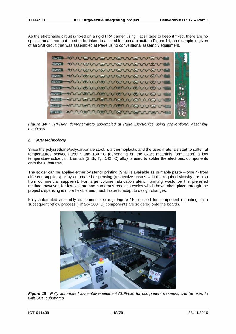
As the stretchable circuit is fixed on a rigid FR4 carrier using Tacsil tape to keep it fixed, there are no special measures that need to be taken to assemble such a circuit. In Figure 14, an example is given of an SMI circuit that was assembled at Page using conventional assembly equipment.
Figure 14 : TPVision demonstrators assembled at Page Electronics using conventional assembly machines
b. SCB technology Since the polyurethane/polycarbonate stack is a thermoplastic and the used materials start to soften at temperatures between 150 ° and 180 °C (depending on the exact materials formulation) a low temperature solder, tin bismuth (SnBi, Tm=142 °C) alloy is used to solder the electronic components onto the substrates. The solder can be applied either by stencil printing (SnBi is available as printable paste – type 4- from different suppliers) or by automated dispensing (respective pastes with the required vicosity are also from commercial suppliers). For large volume fabrication stencil printing would be the preferred method, however, for low volume and numerous redesign cycles which have taken place through the project dispensing is more flexible and much faster to adapt to design changes. Fully automated assembly equipment, see e.g. Figure 15, is used for component mounting. In a subsequent reflow process (Tmax= 160 °C) components are soldered onto the boards.
Figure 15 : Fully automated assembly equipment (SiPlace) for component mounting can be used to with SCB substrates.
TERASEL ICT Large-scale integrating project Deliverable D7.12 – Part 1
ICT-611439 - 19/70 - 25.11.2016
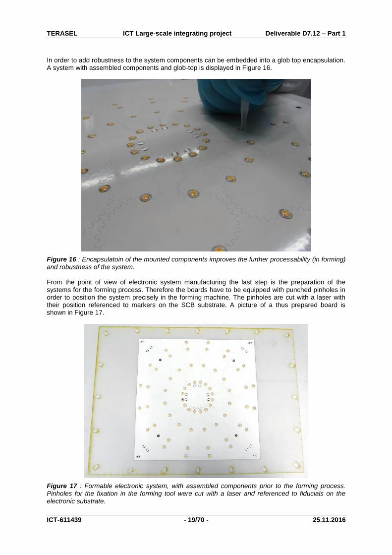
In order to add robustness to the system components can be embedded into a glob top encapsulation. A system with assembled components and glob-top is displayed in Figure 16.
Figure 16 : Encapsulatoin of the mounted components improves the further processability (in forming) and robustness of the system. From the point of view of electronic system manufacturing the last step is the preparation of the systems for the forming process. Therefore the boards have to be equipped with punched pinholes in order to position the system precisely in the forming machine. The pinholes are cut with a laser with their position referenced to markers on the SCB substrate. A picture of a thus prepared board is shown in Figure 17.
Figure 17 : Formable electronic system, with assembled components prior to the forming process. Pinholes for the fixation in the forming tool were cut with a laser and referenced to fiducials on the electronic substrate.
TERASEL ICT Large-scale integrating project Deliverable D7.12 – Part 1
ICT-611439 - 20/70 - 25.11.2016
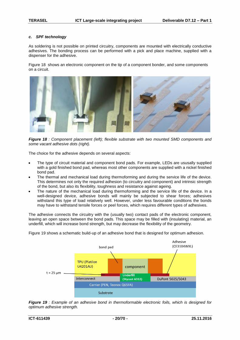
c. SPF technology As soldering is not possible on printed circuitry, components are mounted with electrically conductive adhesives. The bonding process can be performed with a pick and place machine, supplied with a dispenser for the adhesive. Figure 18 shows an electronic component on the tip of a component bonder, and some components on a circuit.
Figure 18 : Component placement (left); flexible substrate with two mounted SMD components and some vacant adhesive dots (right). The choice for the adhesive depends on several aspects:
The type of circuit material and component bond pads. For example, LEDs are ususally supplied with a gold finished bond pad, whereas most other components are supplied with a nickel finished bond pad.
The thermal and mechanical load during thermoforming and during the service life of the device. This determines not only the required adhesion (to circuitry and component) and intrinsic strength of the bond, but also its flexibility, toughness and resistance against ageing.
The nature of the mechanical load during thermoforming and the service life of the device. In a well-designed device, adhesive bonds will mainly be subjected to shear forces; adhesives withstand this type of load relatively well. However, under less favourable conditions the bonds may have to withstand tensile forces or peel forces, which requires different types of adhesives.
The adhesive connects the circuitry with the (usually two) contact pads of the electronic component, leaving an open space between the bond pads. This space may be filled with (insulating) material, an underfill, which will increase bond strength, but may decrease the flexibility of the geometry. Figure 19 shows a schematic build-up of an adhesive bond that is designed for optimum adhesion.
Figure 19 : Example of an adhesive bond in thermoformable electronic foils, which is designed for optimum adhesive strength.

TERASEL ICT Large-scale integrating project Deliverable D7.12 – Part 1
ICT-611439 - 21/70 - 25.11.2016
3. Polymer application a. Injection moulding Polymer application is dedicated to the implementation of injection moulding process in order to overmould the stretchable electronics circuits. This process, developed by the Centre Industriel de la Plasturgie et des Composites (IPC) enables the manufacturing of 3D rigid polymer parts containing several embedded electric and electronic functions. In order to achieve this result, several challenges have to be tackled, in particular:
The materials compatibility between the electronic system and the polymer part
The functionality of the electronic circuit and components after overmoulding
The stretchability of the electronic film during the process Materials compatibility study The analysis of the compatibility between materials and processes is the first challenge to be tackled. This validation is mandatory in order to ensure an optimal integration of the stretchable electronic functions in the final 3D plastic parts. Several combinations of stretchable electronics elements (substrates, components, etc) and overmoulding materials (ABS/PC, PC, PBT, TPU) are evaluated using a dedicated flat test vehicle.
Figure 20 : Vertical injection moulding machine for overmoulding trials
Figure 21 : Functional LED on PCB after overmoulding with PC
For samples with electronic components, the functionality of the devices is checked after overmoulding: light emission for LED (Figure 21), resistance measurement, etc. Visual inspection reveals local damage on soldering and components near the injection gate, related to polymer material temperature and pressure. Peeling test are also performed in order to characterize the adhesion with the injected material: best adhesion results are obtained for ABS / PC on Krystalflex foil, and PC on Platilon foil. Metalized structures distortion and resulting design rules Local damaging of stretchable electronics near the injection gate during overmoulding is observed on Platilon film with Cu dot matrix samples. Thus, a specific analysis of the pattern distortion due to the injection process is carried out, focusing on two parameters: the injected polymer material viscosity, and the injection speed. Two grades of PC are compared: Makrolon 2207 (melt mass-flow rate (MFR) of 38 g/(10 min)), and Calibre 300-15 (MFR of 15 g/(10 min)). With the same set of injection parameters, the viscous material induces much higher damages than the fluid material, as depicted in Figure 22 and Figure 23. With the fluid material, the injection speed can be increased up to the machine limits without inducing any visible damage on the foil. On the contrary, for the viscous material, the injection speed needs to be decreased down to 10 cm
3/s in order to avoid the foil
distortion.

TERASEL ICT Large-scale integrating project Deliverable D7.12 – Part 1
ICT-611439 - 22/70 - 25.11.2016
Overmoulding trials involving various injection speed values reveal that with viscous material like Calibre, the injection speed greatly influences the distortion of the film near the injection gate. At high injection speed, the Platilon foil is greatly damaged, inducing large displacement of Cu dots. This behavior can be explained by the higher pressure and temperature (due to material self-heating) applied on the film at high injection speed.
Figure 22 : Overmoulding with Makrolon: almost no distortion
Figure 23 : Overmoulding with Calibre: local large distortion
Figure 24 : Overmoulded sam-ple with deflection structure
In order to avoid the foil damaging near the injection gate, several solutions are suggested and implemented. The most efficient approach is to integrate a specific Cu structure in front of the injection gate (Figure 24). These structures can be manufactured at the same time as the rest of the electronic circuit. Different design of so-called “deflection structures” are implemented on Cu dot matrix samples and tested, clearly showing their efficiency. Stretchability of the electronics on 3D-shaped test vehicles In order to evaluate the compatibility of stretchable electronics films with 3D polymer parts manufacturing processes, a specific 3D test vehicle is proposed. A dedicated mould enabling a combination of thermoforming and overmoulding in the same tool is used on a Billion Hercule 2000 (320 Tons) injection moulding machine. Evaluations are performed using two PC materials: Makrolon 2207, and Lexan LUX 2010T 11204. Thermoforming of TPU foils is difficult, due to the softness of the material. The heated TPU foils tend to collapse from the mould cavity after the thermoforming step. With an additional PC layer, the stretchable electronics samples reach a sufficient stiffness to retain their 3D-shape after thermoforming. However, PC needs high thermoforming temperature, resulting in an excessive heating of the TPU. For SCB and SPF samples, the PC layer is applied on only one side of the material stack, as summarized in Table 1. This leads to an inevitable damaging of the TPU layer, either by sticking to the mould or due to the injected material, depending on the processing configuration. In the case of SMI samples, embedded on both sides with PC layers, the overheated TPU layer is fully protected. Thus, this configuration offers the best results in terms of process compatibility.
SMI SCB SPF
PC 125µm
TPU 100µm TPU 50µm TPU 100µm
OSRAM 0603 CHIP LED
Copper 18µm Copper 35µm Silver ink 10µm
Polyimide 50µm Soldermask 30µm PEN 125µm
TPU 100µm TPU 100µm PC 250µm
PC 125µm PC 250µm
Table 1 : Material stack for SMI, SCB, and SPF technologies on LED circuit samples for 3D overmoulding

TERASEL ICT Large-scale integrating project Deliverable D7.12 – Part 1
ICT-611439 - 23/70 - 25.11.2016
A specific circuit design for the 3D test vehicle, with meander-shaped conductive tracks and LEDs, is designed. The electronic samples are manufactured with the 3 technologies, according to the material stack described in Table 1. The overmoulding is performed using polycarbonate material. Figure 25 depicts a functional SMI LED circuit after thermoforming and overmoulding. The LED circuit is fully embedded between the foil and the injected polycarbonate, resulting in a smooth part surface. The material stack, in particular involving PC layers, enables the foil to keep its 3D shape after forming. The functionality of the circuit is validated, even in the areas with small radius of curvature (down to 1 mm). High stretchability on the meanders is also highlighted (up to 65%).
Figure 25 : SMI circuit after thermoforming and overmoul-ding
Figure 26 : SCB circuit after pre-heating and overmoulding
Figure 27 : SPF circuit after pre-heating and overmoulding
In the case of SCB samples (Figure 26), the thermoforming step reveals the lack of stretchability of the soldermask beneath the LED. In order to avoid the cracking of this material during the process, a specific local reinforcement is required, or a pre-heating before overmoulding can be applied instead of the thermoforming. However, this second approach induces wrinkles on the final part. The design of the SPF samples (Figure 27) includes only one layer of PC opened around each LED: in these areas, the unprotected TPU layer can be damaged during the foil heating, and result in holes preventing the proper thermoforming. In addition, a delamination is often observed between the TPU and the PC layers, starting in the LED area and spreading along the meanders. As for SCB samples, a pre-heating can be performed instead of the thermoforming, in order to limit these risks. In conclusion, the comparative analysis of the three stretchable electronics technologies reveals clear behaviour differences during thermoforming and overmoulding. The best compatibility is obtained for SMI samples. Promising integration results are nonetheless obtained with SCB and SPF samples, with identified potential improvements.
b. Large area overmolding SINTEX NP focused on large area overmolding, in preparation for the industrial stage of the TERASEL project. The first step was to make an injection mould embedding special features to hold a plastic foil in the cavity before injection of the polymer. The mould allows production of a 285 x 385 mm part, 3 mm thickness. These dimensions have been chosen to fit the SINTEX NP thermoforming machine clamping frame. Injection hot runner nozzle was first located at the centre of the part, but was later on shifted to one side of the cavity. This mould is intended for mounting on a horizontal 400 T press, leading to a vertical orientation of the cavity. Features to hold the foil are vacuum nozzles and punching tips at each corner. Some results are enumerated here bellow:
The flowing melted material inside the mould cavity lead to a localized degradation of the substrate in front of the injection gate. Therefore, tracks and components must be about 30mm away from the injection gate.
Also, an effective way to reduce such damages is to use a large side gate.

TERASEL ICT Large-scale integrating project Deliverable D7.12 – Part 1
ICT-611439 - 24/70 - 25.11.2016
Important consideration is also the kind of material used in the substrate sheet. Indeed, injected material may soften and even melt the overmolded sheet. In some cases, this results to wrinkles on the substrate. To avoid this effects, a right choice of all the involved materials in the final part must be done. For example, while a 300 µm PU sheet is rather easily overmolded by a PC on a small area (using a proper mould design), it’s almost impossible on a large area as in the above described mould. One way to solve such issues is to laminate a protective layer on the sheet and then inject the thermoplastic material on this face. This protective layer must be stiffer than the original functional sheet.
Using proper injection settings and materials, tracks and components are not physically damaged by this process. However, due to the high maximum temperature peak and high pressure they endure during overmolding, the most sensitive components must be carefully tested afterward. This has been done in reliability tests on small samples overmolded by IPC.
4. Forming process a. High pressure forming In 1984, Curt Niebling founded the tool-making company Niebling-Junior, specializing in processing plastics. In 1989, the crucial breakthrough came with the patented invention of isostatic high pressure forming (HPF), (also known as the „Niebling process“), which allowed the forming of different plastic films for the first time. Today, Niebling is a worldwide leading provider of solutions for forming technology made in Germany. The contactless heating system warms the film on both sides to the exact pre-defined temperature. As opposed to thermoforming, the film is heated up only to its glass transition temperature in order to keep the core „stable“ and thus clearly attain higher repeatable accuracies while keeping distortion low. This is especially important in achieving optimum results in position printing on film. The actual forming occurs through heated and compressed air (up to 300 bar), that „presses“ on the film without coming into contact with the surface of the film. This enables visible parts to be processed, for example films with piano black or a hard coating that partially require a follow-up treatment with UV curing. Due to its modular set-up, Niebling forming systems can be flexibly configured based on customer specifications. From the semi-automated system with manual loading and film removal up to fully automated high-end systems, each system is adjusted to your project with the assistance of our experts. All the steps can be run in one single in-line process with assembly robots and conveyor belt solutions. Follow-up treatments with UV radiation as well as the punching of films and inspection with high-resolution cameras are possible, for a 24/7 operation. An industrial system control unit and process monitoring allows to minimize manpower for running operations and to monitor them remotely. The well-developed „Niebling Process“ offers totally new options in design and functionality. Classic coating, printing or galvanizing options are being replaced more and more by the in-mold process. Foil Insert Molding (FIM) and In-Mold Labeling (IML) offer special benefits here when compared to conventional processes. In the case of In-Mold Electronics (IME), electronic, optic and sensory parts are integrated into the plastic films and are already formed ready for operation. Surface structures or even printed images remain reproducible in the high-pressure forming process, including sharp details and molding radii. The automobile industry sets high quality demands, along with a high level of cost awareness. Otherwise, innovation and design rank first. The high-pressure process answers to all demands with one solution. Three-dimensional clock faces, switch edgings and panels are only a small excerpt of the parts manufactured using the „Niebling Process“. In the sports and consumer goods industry, the trend is clearly towards printed designs and shapes that are exactly produced with the HPF process. Industrial designers now have fully new design freedom to construct electrical and medical equipment using isostatic high pressure forming. Niebling designs and builds the molds and cutting tools needed for the process on demand in their own tool construction department. If required, they will also provide support in the design and building
TERASEL ICT Large-scale integrating project Deliverable D7.12 – Part 1
ICT-611439 - 25/70 - 25.11.2016
of injection molding tools. Before investing in a high pressure forming system, Niebling offers the option of using their available capacities for a „one-off production“. High Pressure Forming provides a wide range of applications. Classical forming of all kinds of plastic films:
Utilization of various materials
Functional integration
Integration of conductive structures
Over forming on carrier / molded parts
Forming of material thicknesses up to 12mm
Essential advantages and characteristics:
High positioning accuracy
Low material distortion
High Pressure – low forming temperature
The Forming Process contains 5 phases
Tempering / Heating (Pre-warming, Heating)
Closing
High Pressure Phase
Inflow
Dwell time
Evacuation
Opening / Ejection
Removal
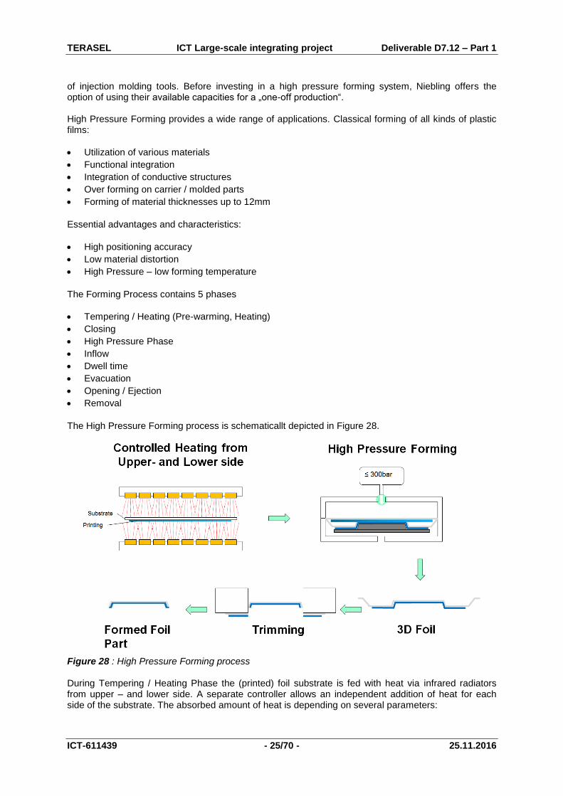
The High Pressure Forming process is schematicallt depicted in Figure 28.
Figure 28 : High Pressure Forming process During Tempering / Heating Phase the (printed) foil substrate is fed with heat via infrared radiators from upper – and lower side. A separate controller allows an independent addition of heat for each side of the substrate. The absorbed amount of heat is depending on several parameters:

TERASEL ICT Large-scale integrating project Deliverable D7.12 – Part 1
ICT-611439 - 26/70 - 25.11.2016
Radiation temperature of the heater elements
Heating time
Reflection rate of the film substrate
Surrounding temperature level / Substrate temperature:
The higher the set heater temperature and the longer the heating time, the higher the substrate
temperature and the bigger the depth of heat penetration into the substrate.
Depending on substrate type and part geometry, the substrate is heated up to the glass transition
temperature and over.
Therefore: The heating system allows a part specific tempering and profile (depending on part
geometry, material, ink system).
The compiled amount of heat over time is depending on the absorption rate of the substrate
material and the printed ink layers.
Dark or black areas heat up quicker than light or reflective areas.
Different materials have different absorption rates and therefore heat up differently.
Different materials and ink types end up in an immense amount of different combination options
for each and every application.
Therefore: Every application needs a specific parameter set
The part specific temperature settings for new applications typically have to be developed in
iteration.
The usage of an optional infrared camera is very helpful in the development of an optimized
temperature distribution and parameter set.
The camera scans the warmed film directly after it leaves the heating and prior to entering the
forming station and provides an IR picture to the user screen.
The temperature of the forming tool contributes as well an important factor to the forming result, as
it influences the temperature transition of the film substrate.
A high tool temperature reduces the cooling effect of the film during the forming process and
supports a defined shaping of geometrical details.
However, a too high tool temperature can lead to a damage of both the substrate material and the
printed ink layers.
b. Vacuum forming SINTEX NP has performed vacuum thermoforming on several sheet materials, from bare PU to overmolded composite PU/PC sheets with copper or ink traces and components. The goal was to test feasibility to form these materials, and specifically the composite and overmolded foils. Theses samples have been mainly produced for stretching and reliability characterization. Compared to usual thermoforming of sheets made of a single material, the machine settings must be more accurate. Indeed, TERASEL sheets can be considered as composite, each layer having its own behaviour against melting and stretching. Moreover, mostly depending on the thermoplastic substrate colour, embedded tracks and components may have a highly different infrared radiation absorption and heat diffusion, leading to hot or cold localized areas. This particularity had to be taken into account when thermoforming such sheets. Some design rules have been identified:
For laminated foils, it is mandatory to avoid trapping air in-between two layers, even micro-bubbles. When thermoforming, such trapped air results in bubbles, large delamination areas, and sometimes blisters.
Also, for the same reasons, drying of the sheet is mandatory, and finger traces must be avoided prior to forming.
Any mark on the foil is accentuated by the thermoforming process. For example, on overmolded foils, ejector marks must be avoided.
TERASEL ICT Large-scale integrating project Deliverable D7.12 – Part 1
ICT-611439 - 27/70 - 25.11.2016
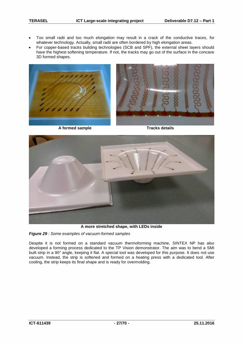
Too small radii and too much elongation may result in a crack of the conductive traces, for whatever technology. Actually, small radii are often bordered by high elongation areas.
For copper-based tracks building technologies (SCB and SPF), the external sheet layers should have the highest softening temperature. If not, the tracks may go out of the surface in the concave 3D formed shapes.
A formed sample Tracks details
A more stretched shape, with LEDs inside
Figure 29 : Some examples of vacuum-formed samples Despite it is not formed on a standard vacuum thermoforming machine, SINTEX NP has also developed a forming process dedicated to the TP Vision demonstrator. The aim was to bend a SMI built strip in a 90° angle, keeping it flat. A special tool was developed for this purpose. It does not use vacuum. Instead, the strip is softened and formed on a heating press with a dedicated tool. After cooling, the strip keeps its final shape and is ready for overmolding.

TERASEL ICT Large-scale integrating project Deliverable D7.12 – Part 1
ICT-611439 - 28/70 - 25.11.2016
CAD view of a prototype forming tool A 90° bended strip with lighting LEDs
Figure 30 : Dedicated tool developed for the TP Vision demonstrator
5. Test and repair methodology Specific process requirements resulting from the forming process, i.e. the elongation due to the forming process at a given position of a product, were tested and investigated using test vehicles with different degrees on complexity. At an initial level test were conducted with simple dot matrix structures, which were subsequently measured. In a next step various wave or meander layouts were subjected to forming tests and optimized towards a lean but robust circuit layout of the overall system. At different steps in the fabrication chain visual, x-ray and electrical tests are implemented in order to achieve as high as possible a fabrication yield. An example of an x-ray inspection is shown in Figure 31.
Figure 31 : X-ray inspection of assembled components revealing shorts between bond pads. Repair of the formable systems is possible only in certain stages of the fabrication process. A defective solder interconnection can be repaired by de-soldering and manual repair. However, once components are embedded in a glob-top, repair without disruptive destruction of the system is no longer possible. For each of the fabrication methodologies SMI, SCB or SPF based formable electronics a proper fabrication chain was established with intermittent test procedures. In this way a high process robustness was achieved and the necessary repair cycles reduced to a minimum.

TERASEL ICT Large-scale integrating project Deliverable D7.12 – Part 1
ICT-611439 - 29/70 - 25.11.2016
4.3 Work package 3 : Process analysis and characterization A. Work package objectives The activities in this Work package 3 were situated in different fields:
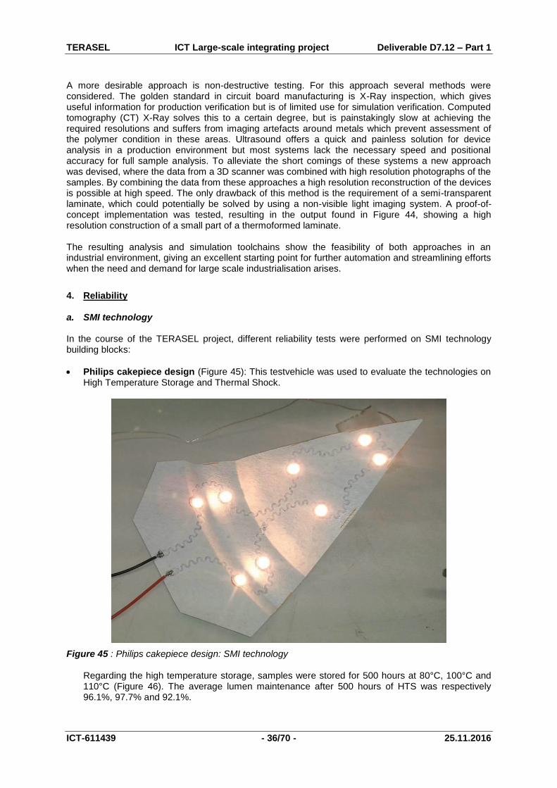
Reliability test vehicles were produced using the technologies developed in work package 2. They were subjected to classic reliability tests like hot humidity, thermal cycling, etc. By this, shortcomings in the technologies could be identified. These tests helped to improve the technologies to make them ready to be used in the demonstrators.
Basic components were realized: general building blocks like stretchable interconnects and more dedicated building blocks like the 90 degree bend for the TPVision demonstrator
Methodologies were created to analyse formed samples by scanning them, processing the information and relating them the mechanical models
Design rules were created for 2.5 D electronic circuits based on experiments and knowledge gathered during the construction of the demonstrators.
B. Major achievements 1. Technology basic building blocks a. Stretchable interconnects There was already a lot of knowledge available in the consortium on the design of stretchable interconnects. Every stretchable interconnect can be defined by its width, radius and angle (Figure 32)
Figure 32 : Definition of a stretchable interconnect Within the TERASEL project, different testvehicles (Figure 33) were developed to identify which designs for the meanders are best working in relation to the deformation of the plastic (Figure 34). As meanders were designed in the past for cyclic deformations, now they should work for a 1 time deformation.
R
w
α

TERASEL ICT Large-scale integrating project Deliverable D7.12 – Part 1
ICT-611439 - 30/70 - 25.11.2016
Figure 33 : Testvehicle including different variations of meanders Parameters for R, α and w were determined in function of a given strain.
Figure 34 : Example of the local deformation measurement. Regions of maximum deformation are at the foot of the elliptical shape.
b. Connectors Different connectors have been made in function of the CRF demonstrator using the SCB technology (Figure 35). The main conclusions of the tests were that crimped connectors fulfill the electrical requirements during reliability, but show some mechanical change in humidity storage. This can be solved by over-moulding or casting.

TERASEL ICT Large-scale integrating project Deliverable D7.12 – Part 1
ICT-611439 - 31/70 - 25.11.2016
Figure 35 : Deformable connectors using SCB technology
c. 90 degree bend Within the project, a high number of testvehicles has been made to realize the in-plane 90 degree bend in function of the TPVision demonstrator. The aim is to bend stretchable strips including RGB leds in a flat way. Special tools were made to guide the bending while heating the deformable strip. The main difficulty is to avoid wrinkles appearing during the bending process. Using local cutting of the strip, mechanical flat bending, and controlled remelting of the TPU (with protective Kapton layers in order to avoid the sticking of the TPU), leads to good results. An additional overmoulding step, fixes the strip (Figure 36).
Figure 36 : Testvehicle for the 90 degree bend

TERASEL ICT Large-scale integrating project Deliverable D7.12 – Part 1
ICT-611439 - 32/70 - 25.11.2016
a. Capacitive turning knob As the end-user for this demonstrator, was a company specialed in printed electronics (Quad), the technology chosen to realize this building block was the SPF technology. Different designs have been realized and evaluated, using a direct and indirect method for printing the silver paste to realize the building block. It has been observed that the direct method is simplest to manufacture and most reliable after forming (Figure 37). The indirect method has issues with buckling/compression.
Figure 37 : Building block capacitive turning knob
b. Capacitive touch interfaces Designs proposed by suppliers of capacitive ICs have been modified to get a thermoformable design. This has led to chequered areas for capacitive touch, which have allowed a functional capacitive touch building block (Figure 38). However, the chequered areas lead to a lot of buckling. A layout option for the area filling of capacitive structures which is more appropriate for thermoforming is the “segmented area-filling” has been proposed and evaluated during the project.
Figure 38 : Capacitive sensor structures for wheel and slider realized in SCB technology and subsequently formed with the elliptical forming tool.
c. Integrated LEDs Within Terasel, integration of light elements is done by means of using SMD Leds. A whole range of test vehicles have been realized to proof the feasibility of integrating light elements in thermoformed parts. In Figure 39, we give some examples of testvehicles with integrated lights.

TERASEL ICT Large-scale integrating project Deliverable D7.12 – Part 1
ICT-611439 - 33/70 - 25.11.2016
Figure 39 : Examples of testvehicles with integrated LEDs The overmoulding of LEDs was tested during the project. It was shown that PP/PC overmoulded samples come out without any visible defects (wrinkling, blistering, detachment,…). After cooling, samples have been tested to evaluate the right operation of the LEDs: in case of PC 100% LEDs are still working after injection molding, in case of PP 80% LEDs are still working after injection molding (Figure 40).
Figure 40 : Samples with over-moulded LEDs during operational tests
d. Heat spreading elements Integrated LEDs for lighting application generate a lot of heat. Use of copper as heat distribution material has been evaluated with very good results. A pad design around the LED components has been proposed (Figure 41), designs for large surfaces of thermoformable heatspreaders have been proposed and the use of metal sheets during forming process was demonstrated.
Figure 41 : Dedicated, deformable pad designs for heat dissipation around LED components

TERASEL ICT Large-scale integrating project Deliverable D7.12 – Part 1
ICT-611439 - 34/70 - 25.11.2016
2. Design rules In the course of the TERASEL project, a set of design rules to make thermoplastically deformed electronic circuits has been collected. The design rules are coming from experience with the testvehicles and demonstrators that were produced and evaluated in the course of the project. The design rules include:
Rules for designing an electronic circuit which is meant to be one time deformable in the end. As a starting point for the design rules, the rules were taken from dynamically deformable circuits. They were evaluated and adjusted when needed.
Rules for designing forming tools, in order that these tools are compatible with the forming of thermoplastically deformable circuits.
Rules for injection moulding tools, in order that these tools are compatible with the overmoulding of electronic circuits.
During the making of the demonstrators, a lot of design iterations took place. We collected all design data and collected what worked and did not work. An example is given below, where for the Philips power balance demonstrator, a lot of design iterations were made in order to position the LED in the middle after forming took place. In every design, the design of the stretchable interconnects is different (Figure 42).
Figure 42 : Design iterations including different stretchable interconnect designs for the Philips power balance demonstrator
3. Simulation To achieve industrialisation of a new technology having a software toolchain to assist with product design is an important aspect. For the TERASEL project the main focus of this effort was on predictive simulation of circuit placement, which helps the circuit designer correctly place the circuit elements on the flat substrate to achieve a desired position on the final deformed object. A secondary aspect of this is measuring and comparing samples to these simulation results; this requires an accurate measurement system capable of achieving the required resolution over a large volume. The first aspect, simulation, quickly branches into two possible paths. A full-fledged multi-physics simulation is an attractive option, and would lead to a lot of interesting data. But solving such a complex system takes tremendous computational effort, and in many cases would take days or weeks to solve on anything but the fastest computational clusters. Since these aren’t widely available within industry an alternative path was taken. By simplifying the problem to something which is possible to run quickly on a desktop computer useful information can still be extracted. This approach is more useful for a circuit designer because it gives rapid – although less exact – feedback on design choices. To achieve this proposed simulation methodology a commercially available simulation engine (Accuform T-SIM) was used. Because it operates on the “conservation of volume” principle that holds true for most thermoforming operations a simple modelling approach to implement features inside the polymer is to locally modify the polymer temperature at the start of the simulation. For example a rigid
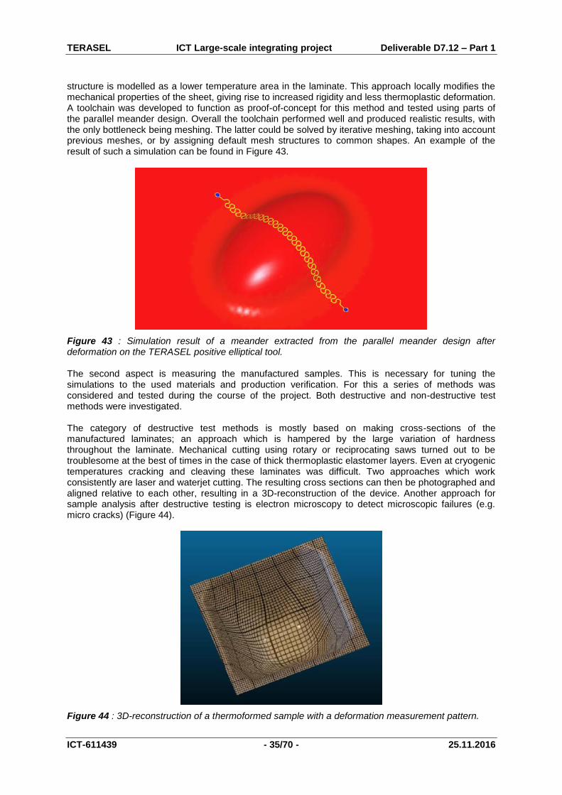
TERASEL ICT Large-scale integrating project Deliverable D7.12 – Part 1
ICT-611439 - 35/70 - 25.11.2016
structure is modelled as a lower temperature area in the laminate. This approach locally modifies the mechanical properties of the sheet, giving rise to increased rigidity and less thermoplastic deformation. A toolchain was developed to function as proof-of-concept for this method and tested using parts of the parallel meander design. Overall the toolchain performed well and produced realistic results, with the only bottleneck being meshing. The latter could be solved by iterative meshing, taking into account previous meshes, or by assigning default mesh structures to common shapes. An example of the result of such a simulation can be found in Figure 43.
Figure 43 : Simulation result of a meander extracted from the parallel meander design after deformation on the TERASEL positive elliptical tool. The second aspect is measuring the manufactured samples. This is necessary for tuning the simulations to the used materials and production verification. For this a series of methods was considered and tested during the course of the project. Both destructive and non-destructive test methods were investigated. The category of destructive test methods is mostly based on making cross-sections of the manufactured laminates; an approach which is hampered by the large variation of hardness throughout the laminate. Mechanical cutting using rotary or reciprocating saws turned out to be troublesome at the best of times in the case of thick thermoplastic elastomer layers. Even at cryogenic temperatures cracking and cleaving these laminates was difficult. Two approaches which work consistently are laser and waterjet cutting. The resulting cross sections can then be photographed and aligned relative to each other, resulting in a 3D-reconstruction of the device. Another approach for sample analysis after destructive testing is electron microscopy to detect microscopic failures (e.g. micro cracks) (Figure 44).
Figure 44 : 3D-reconstruction of a thermoformed sample with a deformation measurement pattern.
TERASEL ICT Large-scale integrating project Deliverable D7.12 – Part 1
ICT-611439 - 36/70 - 25.11.2016
A more desirable approach is non-destructive testing. For this approach several methods were considered. The golden standard in circuit board manufacturing is X-Ray inspection, which gives useful information for production verification but is of limited use for simulation verification. Computed tomography (CT) X-Ray solves this to a certain degree, but is painstakingly slow at achieving the required resolutions and suffers from imaging artefacts around metals which prevent assessment of the polymer condition in these areas. Ultrasound offers a quick and painless solution for device analysis in a production environment but most systems lack the necessary speed and positional accuracy for full sample analysis. To alleviate the short comings of these systems a new approach was devised, where the data from a 3D scanner was combined with high resolution photographs of the samples. By combining the data from these approaches a high resolution reconstruction of the devices is possible at high speed. The only drawback of this method is the requirement of a semi-transparent laminate, which could potentially be solved by using a non-visible light imaging system. A proof-of-concept implementation was tested, resulting in the output found in Figure 44, showing a high resolution construction of a small part of a thermoformed laminate. The resulting analysis and simulation toolchains show the feasibility of both approaches in an industrial environment, giving an excellent starting point for further automation and streamlining efforts when the need and demand for large scale industrialisation arises.
4. Reliability a. SMI technology In the course of the TERASEL project, different reliability tests were performed on SMI technology building blocks:
Philips cakepiece design (Figure 45): This testvehicle was used to evaluate the technologies on High Temperature Storage and Thermal Shock.
Figure 45 : Philips cakepiece design: SMI technology
Regarding the high temperature storage, samples were stored for 500 hours at 80°C, 100°C and 110°C (Figure 46). The average lumen maintenance after 500 hours of HTS was respectively 96.1%, 97.7% and 92.1%.

TERASEL ICT Large-scale integrating project Deliverable D7.12 – Part 1
ICT-611439 - 37/70 - 25.11.2016
After 500 hours all LEDs are still operational
80�C
100�C110�C
Figure 46 : SMI samples after 500 hours storing at high temperatures
For the thermal shock tests, light-up tests were performed on all samples and after 500 hours, all LEDs were still operational.
90 degree bend samples: Samples were subjected to thermal cycling having a temperature profile defined as -55°C to 125°C with 20 minute dwell time. 500 cycles were performed without noticable increase in trace resistance and samples still functional after 500 cycles..
b. SCB technology Polyurethane under extended temperature and temperature cycling load. A discernible yellowing (along with increased absorbance of light) of the material is a definitive exclusion criterion of polyurethanes as topmost layer in consumer applications. In subsequent build-ups typically an additional top-layer was applied in the build-up, which provides the required optical and aesthetical robustness. Even worse was the development of glob top encapsulations which became dark brown after extended reliability stressing conditions. This is however not a basic problem of the overall approach. There is a good chance to solve such issues by using other material formulations and eventually alternative material suppliers. In total SCB based formable systems performed satisfactory from an electrical and mechanical point of view. Only drawbacks are materials related issues as described above.
c. SPF technology The SPF technology comprises several process steps: (screen) printing of conductive circuitry, laser cutting of the printed structure, component mounting with conducting adhesive, lamination and thermoforming. Most of these steps are well-developed and give reliable results. The intrinsic stretchability under thermoforming conditions of the paste itself for instance was determined to be 80 – 100 %. From the experiments with the turning knob demonstrators, the paste structure on the edge experiences a stretch upon thermoforming reaching 100 % and is still fully functional in conductivity after thermoforming. A relatively unknown factor is the bonding of components. As the thermoforming is accompanied by unusual and challenging mechanical load (a combination of tensile, shear and peel forces), a separate evaluation track was dedicated to the effect of bonding parameters on the performance of the adhesive bonds during thermoforming. Basic evaluation was done in shear and flex tests; herewith, the effect of several bond parameters was measured, and the optimum combination of parameters was investigated. After that, thermoforming experiments were performed with a specially developed test vehicle, which contained optimally bonded, standard SMD components with different size, orientation and surface finish. The strain in the regions around the components varied from about 0 to almost 100 %. A function test after the thermoforming revealed what strain levels the glued components could withstand.

TERASEL ICT Large-scale integrating project Deliverable D7.12 – Part 1
ICT-611439 - 38/70 - 25.11.2016
Starting from a frequently used ‘reference adhesive bond’, the following parameters were varied:
Adhesive
Substrate thickness
Printing paste circuitry
Bond thickness
Underfill
Cover layer Shear testing gave the results as shown in the Table 2 below.
Sample parameter
Reference value Actual value Shear force (N)
Reference 5.2 ± 1.6
Circuit DuPont 5025 DuPont 5043 4.9 ± 2.6
Substrate PEN 125 µm PEN 50 µm 7.3 ± 2.6
Adhesive CE 3104 WXL Eccobond CE 8500 0.7 ± 0.4
CE 3104 WXL Ablebond 2030 SC 3.3 ± 1.0
Bond thickness 25 µm 50 µm 10.4 ± 3.0
Underfill No underfill Eccobond UF 3811 13.0 ± 2.4
No underfill Stycast A312 18.8 ± 5.0
Bond pad finish Tin (Sn) Gold (Au) 11.3 ± 1.5
Table 2 : Shear test results for bonded SMD components on printed circuitry In the flex test, the samples with bonded components are subjected to repetitive bending. On regular intervals, the electrical resistance of the adhesive bonds are measured. Usually the bonds will fail after a number of flex cycles. Two components orientations were applied, in which the length direction of the components was either parallel or perpendicular to the length direction of the bending roll. The results for all flex tests, with both orientations, are presented in Table 3.
Sample parameter
Actual value Flex test result
Parallel Perpendicular
Reference No defects Ca. 50 % failure after 1000 cycles
Circuit DuPont 5043 No defects Ca. 50 % failure after 1000 cycles
Substrate PEN 50 µm No defects Ca. 30 % failure after 8000 cycles
Adhesive CE 8500 No defects Ca. 90 % failure after 2000 cycles
2030 SC No defects Ca. 70 % failure after 2000 cycles
Bond thickness
50 µm No defects Ca. 30 % failure after 3500 cycles
Underfill UF 3811 No defects Ca. 40 % failure after 200 cycles
A312 No defects No defects
Table 3 : Flex test results for bonded SMD components on printed circuitry. Each flex cycle contains two bending/unbending steps over a 10 mm bending roll. The terms ‘parallel’ and ‘perpendicular’ refer to the length directions of components and bending roll. Adding underfill Stycast A312 to the bond significantly increases performance under mechanical load. Based on the experimental results, the following conclusions can be drawn:
Application of an underfill, preferably Stycast A312, significantly improves bond performance. This holds for both the static load (shear test) and dynamical load (flex test);
Use of a relatively thin substrate may also improve bond performance;
A thicker bond line has a positive effect on bond performance, although it should be noted that this is primarily caused by the fact that a thicker adhesive dot is squeezed out more when the component is pressed onto it. So, the positive effect mainly comes from a surface increase; but at
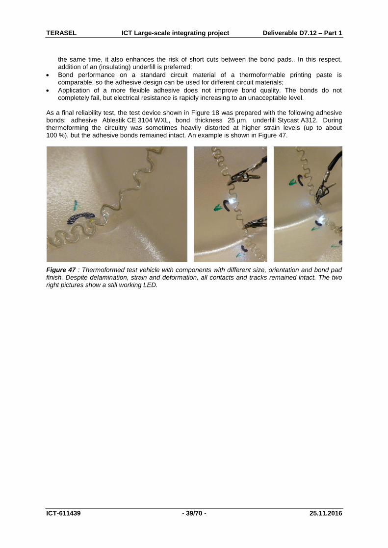
TERASEL ICT Large-scale integrating project Deliverable D7.12 – Part 1
ICT-611439 - 39/70 - 25.11.2016
the same time, it also enhances the risk of short cuts between the bond pads.. In this respect, addition of an (insulating) underfill is preferred;
Bond performance on a standard circuit material of a thermoformable printing paste is comparable, so the adhesive design can be used for different circuit materials;
Application of a more flexible adhesive does not improve bond quality. The bonds do not completely fail, but electrical resistance is rapidly increasing to an unacceptable level.
As a final reliability test, the test device shown in Figure 18 was prepared with the following adhesive bonds: adhesive Ablestik CE 3104 WXL, bond thickness 25 µm, underfill Stycast A312. During thermoforming the circuitry was sometimes heavily distorted at higher strain levels (up to about 100 %), but the adhesive bonds remained intact. An example is shown in Figure 47.
Figure 47 : Thermoformed test vehicle with components with different size, orientation and bond pad finish. Despite delamination, strain and deformation, all contacts and tracks remained intact. The two right pictures show a still working LED.

TERASEL ICT Large-scale integrating project Deliverable D7.12 – Part 1
ICT-611439 - 40/70 - 25.11.2016
4.4 Work package 4 : Industrialization
A. Work package objectives Starting point of this WP are three substrate technologies for stretchable printed circuit boards in lab-scale and technologies for polymer application which have never been applied to those stretchable circuit boards. It was the intention to prepare the transfer of the lab-scale processes into an industrial environment. The second objective was to identify or establish the respective value chain and finally, the third objective referred to cost modelling of the demonstrators. Within this work package the following goals are summarized:
Assessment of the manufacturability of all building blocks in all selected processes
Assessment of the process flow to meet cost requirements and to obtain sufficient yield figures.
Investigate logistics to describe the handling challenges not only within the different production sites, but especially the transfer of semi-finished products from one manufacturer to the other.
B. Major achievements All process flows have been setup in detail. The cost model established by TNO/Holst was executed on a generic test vehicle to compare the different substrate technologies based on the initially generated process flows. The process flows are updated for the final demonstrators and the results – if possible – compared to existing solutions. The technology vs demonstrator selection was performed with a risk based tool of Philips, updated and finished. The output was used to evaluate a Technology Readiness Level at the end of the project to judge the change in TRL from beginning to the end of the project. Based on an evaluation per technology the overall TRL was raised by 2 from 3-4 to 5-6. The process flows have been shown in Section 2 of this report. It was the activity of Work package 4 to identify steps that seemed critical while transferring into an industrial environment. Most of the issues identified during the course of the project were solved directly (a few topics are mentioned at the end of this section). That was based on the close cooperation between institutes and industrial partners. The value chain was created on the realization of the demonstrators, It included the availability of all materials and equipment and also calculations who would be the producer and whether there is request for a supplier of individual process steps due to missing workload for specific equipment. Depending on volume some process steps cannot be run in full capacity thus sub-contracting is the solution. E.g., in terms of base material for SCB technology the lamination of Cu on PU film is only cost effective by a materials supplier who aggregates different.requests. Currently, the inquired volumes do not lead to “realistic” pricing of the base material. Open items and future research Some items are still open at the end of the project:
One common observation was the “missing software tool for design rules”. It is quite clear that, although a number of design rules have been generated, no software tool is available to automatically apply these rules. It was also clear that there was no partner who would be able to generate such a software package as it was also not primarily intended. However, the implementation of design rules relies heavily on the availability of standardized procedures. Thus, software design tools are an identified gap during the project.
A second big issue was the appearance of formats that did not fit with standard equipment formats. E.g. in the case of CRF the lamination and laser cutting equipment at IZM and at ENMECH was not completely sufficient. The formats at PCB or Flex manufacturing are almost
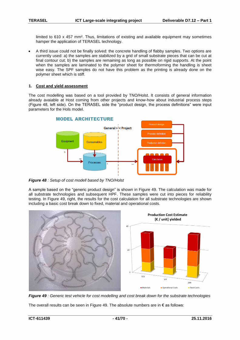
TERASEL ICT Large-scale integrating project Deliverable D7.12 – Part 1
ICT-611439 - 41/70 - 25.11.2016
limited to 610 x 457 mm². Thus, limitations of existing and available equipment may sometimes hamper the application of TERASEL technology.
A third issue could not be finally solved: the concrete handling of flabby samples. Two options are currently used: a) the samples are stabilized by a grid of small substrate pieces that can be cut at final contour cut; b) the samples are remaining as long as possible on rigid supports. At the point when the samples are laminated to the polymer sheet for thermoforming the handling is sheet wise easy. The SPF samples do not have this problem as the printing is already done on the polymer sheet which is stiff.
1. Cost and yield assessment The cost modelling was based on a tool provided by TNO/Holst. It consists of general information already avaiable at Host coming from other projects and know-how about industrial process steps (Figure 48, left side). On the TERASEL side the “product design, the process definitions” were input parameters for the Hols model.
Figure 48 : Setup of cost modell based by TNO/Holst A sample based on the “generic product design” is shown in Figure 49. The calculation was made for all substrate technologies and subsequent HPF. These samples were cut into pieces for reliability testing. In Figure 49, right, the results for the cost calculation for all substrate technologies are shown including a basic cost break down to fixed, material and operational costs.
Figure 49 : Generic test vehicle for cost modelling and cost break down for the substrate technologies The overall results can be seen in Figure 49. The absolute numbers are in € as follows:
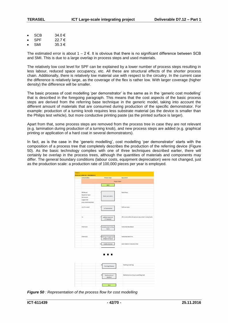
TERASEL ICT Large-scale integrating project Deliverable D7.12 – Part 1
ICT-611439 - 42/70 - 25.11.2016
SCB 34.0 €
SPF 22.7 €
SMI 35.3 € The estimated error is about 1 – 2 €. It is obvious that there is no significant difference between SCB and SMI. This is due to a large overlap in process steps and used materials. The relatively low cost level for SPF can be explained by a lower number of process steps resulting in less labour, reduced space occupancy, etc. All these are structural effects of the shorter process chain. Additionally, there is relatively low material use with respect to the circuitry. In the current case the difference is relatively large, as the coverage of the flex is rather low. With larger coverage (higher density) the difference will be smaller. The basic process of cost modelling ‘per demonstrator’ is the same as in the ‘generic cost modelling’ that is described in the foregoing paragraph. This means that the cost aspects of the basic process steps are derived from the referring base technique in the generic model, taking into account the different amount of materials that are consumed during production of the specific demonstrator. For example: production of a turning knob requires less substrate material (as the device is smaller than the Philips test vehicle), but more conductive printing paste (as the printed surface is larger). Apart from that, some process steps are removed from the process tree in case they are not relevant (e.g. lamination during production of a turning knob), and new process steps are added (e.g. graphical printing or application of a hard coat in several demonstrators). In fact, as is the case in the ‘generic modelling’, cost modelling ‘per demonstrator’ starts with the composition of a process tree that completely describes the production of the referring device (Figure 50). As the basic technology complies with one of three techniques described earlier, there will certainly be overlap in the process trees, although the quantities of materials and components may differ. The general boundary conditions (labour costs, equipment depreciation) were not changed, just as the production scale: a production rate of 100,000 pieces per year is employed.
Figure 50 : Representation of the process flow for cost modelling
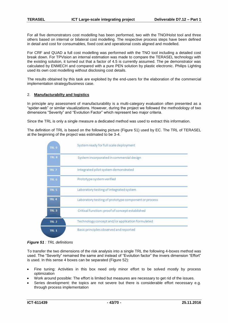
TERASEL ICT Large-scale integrating project Deliverable D7.12 – Part 1
ICT-611439 - 43/70 - 25.11.2016
For all five demonstrators cost modelling has been performed, two with the TNO/Holst tool and three others based on internal or bilateral cost modelling. The respective process steps have been defined in detail and cost for consumables, fixed cost and operational costs aligned and modelled. For CRF and QUAD a full cost modelling was performed with the TNO tool including a detailed cost break down. For TPVision an internal estimation was made to compare the TERASEL technology with the existing solution, it turned out that a factor of 4.5 is currently assumed. The pe demonstrator was calculated by ENMECH and compared with a pure PEN solution by plastic electronic. Philips Lighting used its own cost modelling without disclosing cost details. The results obtained by this task are exploited by the end-users for the elaboration of the commercial implementation strategy/business case.
2. Manufacturabilty and logistics In principle any assessment of manufacturability is a multi-category evaluation often presented as a “spider-web” or similar visualizations. However, during the project we followed the methodology of two dimensions “Severity” and “Evolution Factor” which represent two major criteria. Since the TRL is only a single measure a dedicated method was used to extract this information. The definition of TRL is based on the following picture (Figure 51) used by EC. The TRL of TERASEL at the beginning of the project was estimated to be 3-4.
Figure 51 : TRL definitions To transfer the two dimensions of the risk analysis into a single TRL the following 4-boxes method was used. The “Severity” remained the same and instead of “Evolution factor” the invers dimension “Effort” is used. In this sense 4 boxes can be separated (Figure 52):
Fine tuning: Activities in this box need only minor effort to be solved mostly by process optimization
Work around possible: The effort is limited but measures are necessary to get rid of the issues.
Series development: the topics are not severe but there is considerable effort necessary e.g. through process implementation

TERASEL ICT Large-scale integrating project Deliverable D7.12 – Part 1
ICT-611439 - 44/70 - 25.11.2016
New research: the items are critical and it looks as if a considerable effort is necessary or no vision of an appropriate solution is available. This represents gaps which lead to new research proposals, e.g.
Each of the topics, issues or risks for each technology can be assigned to one of the four boxes.
Figure 52 : 4-box-model to derive TRL from risk analysis In a dedicated workshop the procedure was performed for the basic technologies and the results is shown in Table 4. Additionally, the TRL at the beginning of the project was estimated per technology. There was no dedicated procedure at the beginning to fix the TRL. For the substrate technologies an assessment of the maturity is possible on the results of PLACE-iT. That is the base for the last column in Table 4.
Technology TRL at end of project TRL beginning of project (estimated)
SCB 6 4
SMI 4-6 3-4
SPF 6 3 (technology just started by TNO)
HPF 5 (-6) Low with respect to TERASEL
VM/IM 5 Low with respect to TERASEL
Lamination 4-5 Low with respect to TERASEL
Table 4 : TRL based on workshop at GM 11 in Turin per technology The summary for the evolution through the project is given by Figure 53 indicating that overall the level has been raised by two.
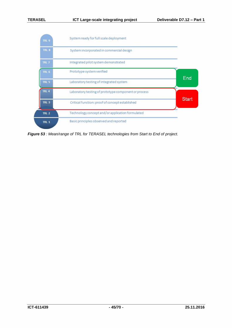
TERASEL ICT Large-scale integrating project Deliverable D7.12 – Part 1
ICT-611439 - 45/70 - 25.11.2016
Figure 53 : Mean/range of TRL for TERASEL technologies from Start to End of project.

TERASEL ICT Large-scale integrating project Deliverable D7.12 – Part 1
ICT-611439 - 46/70 - 25.11.2016
4.5 Work package 5 : Demonstration
A. Work package objectives The objective of this work package is the design, fabrication and evaluation of a number of functional demonstrators, using TERASEL technologies, and paving the way to future products, which can be made in a commercially viable way only by use of the novel TERASEL technology. To show the large business potential of TERASEL technology, 5 different demonstrators have been fabricated in a wide field of applications:
Automotive (Glove box panel with embedded electronics, CRF)
Consumer electronics (TV Ambilight, TP Vision)
Man-machine interfaces (3D touch-wheel button, Quad Industries)
Lighting (Down Light Luminair, Philips)
Household products (Washing machine interface, Plastic Electronic) The first objective of WP5 was to set the functionalities that were needed by the end-users, then the demonstrators were designed to match the functionalities and the technologic capabilities. A first set of prototypes were produced and tested to optimize the process chain. Finally, fully functional devices were fabricated for the reliability testing and the assessment of the functionalities. The final goal was to produce the WP5 demonstrators using the TERASEL established "industrial chains", thus proving the validity and proper operation of these chains. A lot of efforts were done by the end-users to test the demonstrators in terms of functionalities and reliability, in order to get functional devices that can withstand the severe requirements necessary to have a real commercial product. This challenge has really improved the development level of the TERASEL technologies. It is remarkable to notice that each demonstrator has its own features and technical challenges to be faced as it is shown in the following table. Figure 54 depicts graphically how the different demonstrators embody different level of stretch and electronic complexity. In the following parts, a specific description for each demo is provided.
Figure 54 : graphical representation of different levels of stretch and electronics complexity requested by the demonstrators.
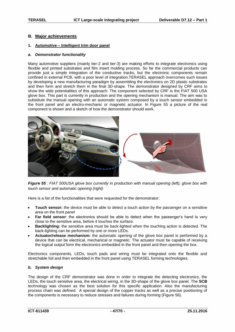
TERASEL ICT Large-scale integrating project Deliverable D7.12 – Part 1
ICT-611439 - 47/70 - 25.11.2016
B. Major achievements 1. Automotive – Intelligent trim door panel a. Demonstrator functionality Many automotive suppliers (mainly tier-2 and tier-3) are making efforts to integrate electronics using flexible and printed substrates and film insert molding process. So far the commercial products can provide just a simple integration of the conductive tracks, but the electronic components remain confined in external PCB, with a poor level of integration.TERASEL approach overcomes such issues by developing a new manufacturing paradigm by assembling the electronics on 2D plastic substrates and then form and stretch them in the final 3D-shape. The demonstrator designed by CRF aims to show the wide potentialities of this approach: The component selected by CRF is the FIAT 500 USA glove box. This part is currently in production and the opening mechanism is manual. The aim was to substitute the manual opening with an automatic system composed by a touch sensor embedded in the front panel and an electro-mechanic or magnetic actuator. In Figure 55 a picture of the real component is shown and a sketch of how the demonstrator should work.
Figure 55 : FIAT 500USA glove box currently in production with manual opening (left), glove box with
touch sensor and automatic opening (right)
Here is a list of the functionalities that were requested for the demonstrator:
Touch sensor: the device must be able to detect a touch action by the passenger on a sensitive area on the front panel
Far field sensor: the electronics should be able to detect when the passenger’s hand is very close to the sensitive area, before it touches the surface.
Backlighting: the sensitive area must be back-lighted when the touching action is detected. The back-lighting can be performed by one or more LEDs.
Actuator/release mechanism: the automatic opening of the glove box panel is performed by a device that can be electrical, mechanical or magnetic. The actuator must be capable of receiving the logical output form the electronics embedded in the front panel and then opening the box.
Electronics components, LEDs, touch pads and wiring must be integrated onto the flexible and stretchable foil and then embedded in the front panel using TERASEL forming technologies. b. System design
The design of the CRF demonstrator was done in order to integrate the detecting electronics, the LEDs, the touch sensitive area, the electrical wiring, in the 3D-shape of the glove box panel. The SCB technology was chosen as the best solution for this specific application. Also the manufacturing process chain was defined. A special design of the copper tracks as well as a precise positioning of the components is necessary to reduce stresses and failures during forming (Figure 56).

TERASEL ICT Large-scale integrating project Deliverable D7.12 – Part 1
ICT-611439 - 48/70 - 25.11.2016
Figure 56 : Layout of the SCB film for the CRF demonstrator c. Demonstrator assembly Fully working demonstrators have been fabricated using SCB substrate technology, lamination and high pressure forming. Electronics film has been assembled on a planar stack and then formed in a 3D shape without damaging the components and losing functionalities (Figure 57). The final outcome is a compact and robust device with embedded electronics and wiring that opens the doors to a new way of thinking the plastic components inside the car: no more as passive parts but as carriers of new functionalities. The smart glove box has been assembled successfully in the dashboard of a FIAT 500 (Figure 58).
Figure 57 : Glove box cover with embedded electronic. The SCB electronic film is integrated in the PC panel. The touch sensitive area is able to detect the user’s touch and then drives the LEDs and opening system

TERASEL ICT Large-scale integrating project Deliverable D7.12 – Part 1
ICT-611439 - 49/70 - 25.11.2016
d. Demonstrator characterisation The glove box panel was tested form different points of view. First, the requested functionalities have been evaluated in different environmental conditions. Then the panels were submitted to different ageing and reliability tests according to the automotive requirements. The functionalities requested have been successfully implemented in the demonstrator. The final assessment of the glove box demonstrator is positive. The remaining open issues are not so critical and are very likely to be solved. The CRF demonstrator is a successful concept that can be extended to many interiors automotive components: the plastic surfaces can be enriched with sensors, actuators, LED, buttons that now need bulky electronic boards and electromechanical switches. The new technology coming out from TERASEL is lighter, more reliable, easier to be shaped by the designers will.
Figure 58 : FIAT 500 dashboard. On the left the standard glove box, on the right the smart glove box with embedded electronics.
2. Consumer electronics – TV Ambilight a. Demonstrator functionality Today’s customers for consumer electronics devices desire maximum functionality and appeal while looking for great value, this also applies to the television market. The visual attractiveness of a television is not only a matter of best viewing experience, but also of its ability to blend in different home environments. The Ambilight
® function in Philips televisions is an important factor in enabling a
better immersive experience. It aims at creating light effects around the television that correspond to the video content, effectively increasing the image canvas when enjoying movies and video in the home.
Figure 59 : Ambilight casting a glow on the wall behind a Philips TV
TERASEL ICT Large-scale integrating project Deliverable D7.12 – Part 1
ICT-611439 - 50/70 - 25.11.2016
At the same time, design trends expect that the television evolves towards ever thinner and slimmer devices. Beyond the challenges to fit all common mechanics and electronics in ever smaller volumes, the Ambilight functionality should not undermine this evolution. In its common implementation, this feature requires a complex set of circuit boards and electrical and mechanical interconnections, that add their own set of constraints that at first seem to go counter to the design statement expectations.
b. System design At the core of the Ambilight system lays a series of LEDs driven by control electronics on a set of rigid circuit boards. This requires a large number of connections and considerable mechanical design effort. If these circuits could be integrated more tightly in the back cover of a television, maybe even fully embedded in the plastic of the back cover, this would open up the next step in size reduction. Now this would require a process which entails both deformation of the circuit and over-moulding in the plastic back cover. Both challenges fit nicely in the objectives of the TERASEL project. Furthermore, as an additional benefit and driver for the innovation, the technique would also open up opportunities to leverage inventory and production optimisations, not only for Ambilight but also in other cases where electronics and interconnections come at a premium, since the mechanical flexibility of the circuits would allow reduction in diversity of parts for different products and has the potential to simplify assembly steps in factories. With TERASEL, methods were investigated to reduce this complexity, and by extension also the cost, while still enabling attractive sleek and thin design propositions. The experiments have concentrated on bending circuit boards at angles of 90° in the plane of the board, and integrating these flexed boards in plastic assemblies for compactness. In view of cost and large quantities for the given application domain in consumer electronics, SMI is considered as the basic flex PCB process. It consists of following main steps :
Process steps
Flex sheet manufacturing
Sheet component placement
Sheet cutting in strips
Strips bending over 90º in plane of strip, clamping
Overmoulding of strips in plastic component
Realization of electrical connections to strips
c. Demonstrator assembly TP Vision defined the corner part of a lighting module of its Ambilight system as its demonstrator. SMI technology was used to produce the LED strips first as straight circuits, followed by realizing a 90º turn by bending/stretching the straight circuit in the corner area, and by embedding the circuit in a thermoplastic polymer. Using a specific tool (a heating press allowing hot bending of the strip that keeps its bent shape after cooling), bending was achieved. LEDs are protected against heat and positioned according to their final position in the TV set back cover. As the carrier flex material is soft, a reinforcement part is needed to keep it flat for the overmoulding step coming next. During over-moulding, the strip is fully embedded in a plastic carrier, safe the LED optical windows and the connectors. After extraction from the mould and cooling, the assembly is ready to be tested and evaluated.

TERASEL ICT Large-scale integrating project Deliverable D7.12 – Part 1
ICT-611439 - 51/70 - 25.11.2016
Figure 60 : Flexible PCB strips in sheet, with components in place
Figure 61 : Bending tool in action, showing flex PCB and protective PC sheet
Figure 62 : Flex PCB after bending, showing working connection and components

TERASEL ICT Large-scale integrating project Deliverable D7.12 – Part 1
ICT-611439 - 52/70 - 25.11.2016
Figure 63 : Flex PCB strip bent over 90º applied to a TV back cover
d. Demonstrator characterisation While from the onset it was clear that the set targets of small radius bend combined with stringent mechanical tolerances would be very challenging for the partners in the project, a number of important steps were realized. Bending over 90° is achieved. Remaining issues were encountered in the overmoulding process, where additional attention was necessary to avoid component damage, wrinkling and positioning mismatches. Following Table 5 gives a synoptic overview of design capabilities with a brief assessment of the achieved results.
Achievements
Bending over 90° in PCB plane Demonstrated
Overmoulding Achieved, with design limitations in turn radius
Connectors integration Achieved, requiring steps to safeguard the mechanical integrity of the connectors during overmoulding
Large size (>1m) of strips Concept can be realized with existing flex techniques to unfold a larger serpentine
Electrical resistance Over large lengths of more than 1 meter, the electrical conductors tend to show excessive resistance. Additional current carrying paths – adjacent or in multiple layers – can alleviate this.
Table 5 : Overview of design capabilities and assessment of results Furthermore, the units have been subjected to environmental stress tests cycling through commercial temperature and humidity ranges without negative effects. Select stress, durability and environmental testing was successful. Overall, the results show the potential for simplification of inventory of parts and assemblies for a wide range of products in which they can be integrated. They also illustrate capabilities of the technology for novel design propositions. From these results, the path to industrialization is very well conceivable, and for all issues identified, a solution is either existing or can be envisioned based on previous experiences in similar domains.
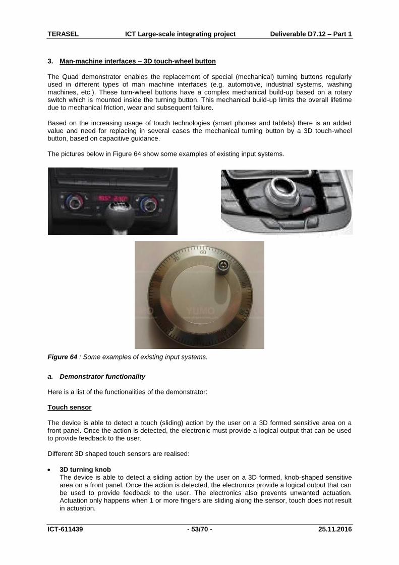
TERASEL ICT Large-scale integrating project Deliverable D7.12 – Part 1
ICT-611439 - 53/70 - 25.11.2016
3. Man-machine interfaces – 3D touch-wheel button The Quad demonstrator enables the replacement of special (mechanical) turning buttons regularly used in different types of man machine interfaces (e.g. automotive, industrial systems, washing machines, etc.). These turn-wheel buttons have a complex mechanical build-up based on a rotary switch which is mounted inside the turning button. This mechanical build-up limits the overall lifetime due to mechanical friction, wear and subsequent failure. Based on the increasing usage of touch technologies (smart phones and tablets) there is an added value and need for replacing in several cases the mechanical turning button by a 3D touch-wheel button, based on capacitive guidance. The pictures below in Figure 64 show some examples of existing input systems.
Figure 64 : Some examples of existing input systems.
a. Demonstrator functionality Here is a list of the functionalities of the demonstrator: Touch sensor The device is able to detect a touch (sliding) action by the user on a 3D formed sensitive area on a front panel. Once the action is detected, the electronic must provide a logical output that can be used to provide feedback to the user. Different 3D shaped touch sensors are realised:
3D turning knob The device is able to detect a sliding action by the user on a 3D formed, knob-shaped sensitive area on a front panel. Once the action is detected, the electronics provide a logical output that can be used to provide feedback to the user. The electronics also prevents unwanted actuation. Actuation only happens when 1 or more fingers are sliding along the sensor, touch does not result in actuation.
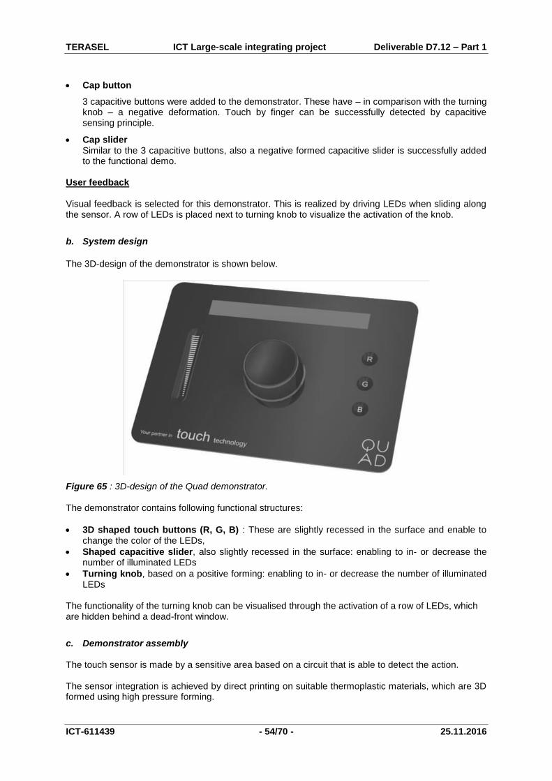
TERASEL ICT Large-scale integrating project Deliverable D7.12 – Part 1
ICT-611439 - 54/70 - 25.11.2016
Cap button
3 capacitive buttons were added to the demonstrator. These have – in comparison with the turning knob – a negative deformation. Touch by finger can be successfully detected by capacitive sensing principle.
Cap slider Similar to the 3 capacitive buttons, also a negative formed capacitive slider is successfully added to the functional demo.
User feedback Visual feedback is selected for this demonstrator. This is realized by driving LEDs when sliding along the sensor. A row of LEDs is placed next to turning knob to visualize the activation of the knob.
b. System design
The 3D-design of the demonstrator is shown below.
Figure 65 : 3D-design of the Quad demonstrator. The demonstrator contains following functional structures:
3D shaped touch buttons (R, G, B) : These are slightly recessed in the surface and enable to change the color of the LEDs,
Shaped capacitive slider, also slightly recessed in the surface: enabling to in- or decrease the number of illuminated LEDs
Turning knob, based on a positive forming: enabling to in- or decrease the number of illuminated LEDs
The functionality of the turning knob can be visualised through the activation of a row of LEDs, which are hidden behind a dead-front window.
c. Demonstrator assembly The touch sensor is made by a sensitive area based on a circuit that is able to detect the action.
The sensor integration is achieved by direct printing on suitable thermoplastic materials, which are 3D formed using high pressure forming.

TERASEL ICT Large-scale integrating project Deliverable D7.12 – Part 1
ICT-611439 - 55/70 - 25.11.2016
Backlighting and driving electronics are integrated on PCB using conventional technologies. The electronics will drive LEDs to provide visual user feedback. These LEDs are implemented with conventional technologies. The capacitive front panel is further integrated – together with the driving electronics – in a housing. The final module is shown in Figure 66.
Figure 66 : Final assembled module of the Quad demonstrator.
d. Demonstrator characterisation The turning knob has many possible applications, therefore general reliability testing under demanding environmental conditions has been done. The turning knob has been successfully submitted to the following test conditions: 1. Accelerated temperature tests
- 100°C - 1000 hours
2. Thermal cycle tests - -40°C / +85 °C – dwell time 30 min @ max temp - 500 cycles
3. High temperature storage
Figure 67 : Final assembled module of the Quad demonstrator.
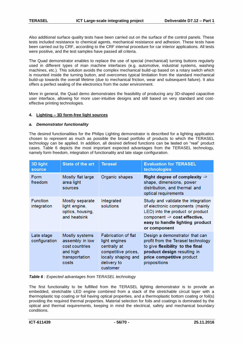
TERASEL ICT Large-scale integrating project Deliverable D7.12 – Part 1
ICT-611439 - 56/70 - 25.11.2016
Also additional surface quality tests have been carried out on the surface of the control panels. These tests included resistance to chemical agents, mechanical resistance and adhesion. These tests have been carried out by CRF, according to the CRF internal procedure for car interior applications. All tests were positive, and the test samples have passed all criteria. The Quad demonstrator enables to replace the use of special (mechanical) turning buttons regularly used in different types of man machine interfaces (e.g. automotive, industrial systems, washing machines, etc.). This solution avoids the complex mechanical build-up based on a rotary switch which is mounted inside the turning button, and overcomes typical limitation from the standard mechanical build-up towards the overall lifetime (due to mechanical friction, wear and subsequent failure). It also offers a perfect sealing of the electronics from the outer environment. More in general, the Quad demo demonstrates the feasibility of producing any 3D-shaped capacitive user interface, allowing for more user-intuitive designs and still based on very standard and cost-effective printing technologies.
4. Lighting – 3D form-free light sources a. Demonstrator functionality The desired functionalities for the Philips Lighting demonstrator is described for a lighting application chosen to represent as much as possible the broad portfolio of products to which the TERASEL technology can be applied. In addition, all desired defined functions can be tested on “real” product cases. Table 6 depicts the most important expected advantages from the TERASEL technology, namely form freedom, integration of functionality and late stage configuration.
Table 6 : Expected advantages from TERASEL technology
The first functionality to be fulfilled from the TERASEL lighting demonstrator is to provide an embedded, stretchable LED engine combined from a stack of the stretchable circuit layer with a thermoplastic top coating or foil having optical properties, and a thermoplastic bottom coating or foil(s) providing the required thermal properties. Material selection for foils and coatings is dominated by the optical and thermal requirements, keeping in mind the electrical, safety and mechanical boundary conditions.

TERASEL ICT Large-scale integrating project Deliverable D7.12 – Part 1
ICT-611439 - 57/70 - 25.11.2016
Another important functionality for the lighting demonstrators is the reliability of the product. This concerns the initial reliability like for the stretchable circuit design that should provide the possibility to take into account the conductor trace and solder joint integrity after stretching. Also the thermo-forming technology should not affect structural integrity of the composite. The reliability during lifetime should be as defined for in the specifications and will be tested accordingly.
Figure 68 : Down light luminaire chosen for the demonstration of TERASEL technology for lighting application
The chosen downlight luminaire as depicted in Figure 68 should fulfil the combination of a central task light with variable beam angle with ambient light at the periphery of the lamp and luminaire, easy connections, and semi-manufactured goods can be stored
b. System design The system design for the Philips Lighting demonstrators is worked out in such a way that it can fulfil the functionalities defined for the Philips demonstrator functionality and in the user specifications. The system design shows how the functionalities are implemented in physical LED application demonstrators. It describes for the lighting demonstrator the size, shape, materials and final construction. In addition, the thermal and optical layout and the processing challenges related to the materials stack have been worked out. The substrate composition, and the forming technologies, are selected. The process flow for the manufacturing of the demonstrators has been worked out. The lighting demonstrator has been chosen to fit in existing application, and has to provide an embedded, stretchable LED engine combined from a stack of the stretchable circuit layer, and a thermoplastic bottom coating or foil(s) providing the required thermal properties. Material selection for foils and coatings is dominated by the thermal and optical requirements, keeping in mind the electrical, safety, optical and mechanical boundary conditions. The lighting demonstrators have also been designed in such a way, that the reliability of the product is provided. This concerns the initial reliability like for the stretchable circuit design that should provide the conductor trace and solder joint integrity after stretching. Also the thermo-forming technology should not affect structural integrity of the composite. This all leads to the choice of system design and TERASEL technologies as described in the Figure 69 below.
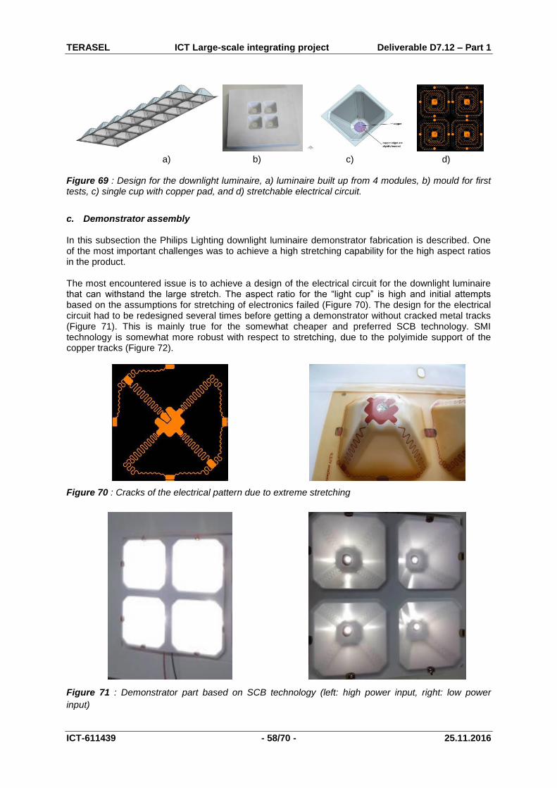
TERASEL ICT Large-scale integrating project Deliverable D7.12 – Part 1
ICT-611439 - 58/70 - 25.11.2016
a) b) c) d)
Figure 69 : Design for the downlight luminaire, a) luminaire built up from 4 modules, b) mould for first tests, c) single cup with copper pad, and d) stretchable electrical circuit.
c. Demonstrator assembly In this subsection the Philips Lighting downlight luminaire demonstrator fabrication is described. One of the most important challenges was to achieve a high stretching capability for the high aspect ratios in the product. The most encountered issue is to achieve a design of the electrical circuit for the downlight luminaire that can withstand the large stretch. The aspect ratio for the “light cup” is high and initial attempts based on the assumptions for stretching of electronics failed (Figure 70). The design for the electrical circuit had to be redesigned several times before getting a demonstrator without cracked metal tracks (Figure 71). This is mainly true for the somewhat cheaper and preferred SCB technology. SMI technology is somewhat more robust with respect to stretching, due to the polyimide support of the copper tracks (Figure 72).
Figure 70 : Cracks of the electrical pattern due to extreme stretching
Figure 71 : Demonstrator part based on SCB technology (left: high power input, right: low power
input)
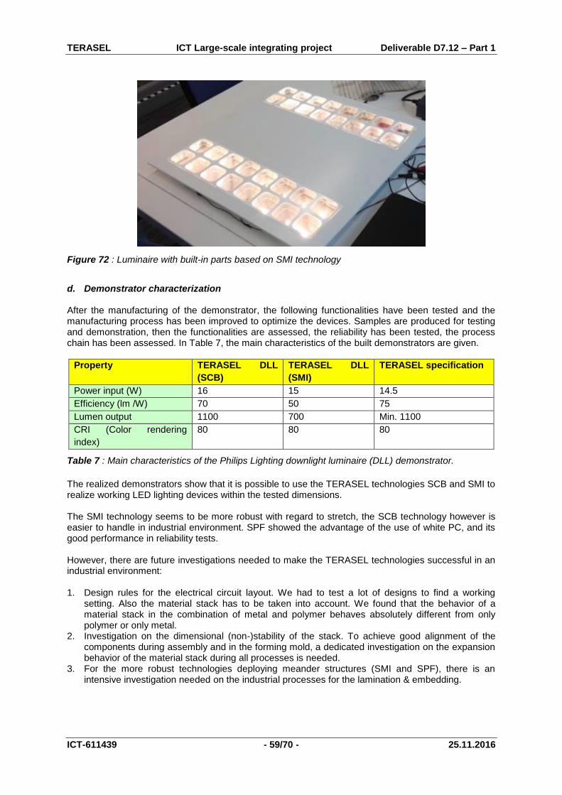
TERASEL ICT Large-scale integrating project Deliverable D7.12 – Part 1
ICT-611439 - 59/70 - 25.11.2016
Figure 72 : Luminaire with built-in parts based on SMI technology
d. Demonstrator characterization After the manufacturing of the demonstrator, the following functionalities have been tested and the manufacturing process has been improved to optimize the devices. Samples are produced for testing and demonstration, then the functionalities are assessed, the reliability has been tested, the process chain has been assessed. In Table 7, the main characteristics of the built demonstrators are given.
Property TERASEL DLL
(SCB)
TERASEL DLL
(SMI)
TERASEL specification
Power input (W) 16 15 14.5
Efficiency (lm /W) 70 50 75
Lumen output 1100 700 Min. 1100
CRI (Color rendering
index)
80 80 80
Table 7 : Main characteristics of the Philips Lighting downlight luminaire (DLL) demonstrator.
The realized demonstrators show that it is possible to use the TERASEL technologies SCB and SMI to realize working LED lighting devices within the tested dimensions. The SMI technology seems to be more robust with regard to stretch, the SCB technology however is easier to handle in industrial environment. SPF showed the advantage of the use of white PC, and its good performance in reliability tests. However, there are future investigations needed to make the TERASEL technologies successful in an industrial environment: 1. Design rules for the electrical circuit layout. We had to test a lot of designs to find a working
setting. Also the material stack has to be taken into account. We found that the behavior of a material stack in the combination of metal and polymer behaves absolutely different from only polymer or only metal.
2. Investigation on the dimensional (non-)stability of the stack. To achieve good alignment of the components during assembly and in the forming mold, a dedicated investigation on the expansion behavior of the material stack during all processes is needed.
3. For the more robust technologies deploying meander structures (SMI and SPF), there is an intensive investigation needed on the industrial processes for the lamination & embedding.
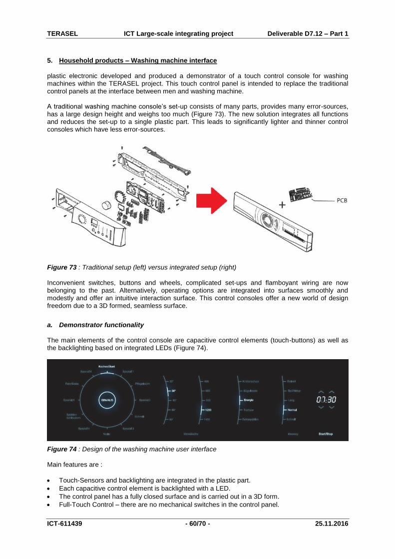
TERASEL ICT Large-scale integrating project Deliverable D7.12 – Part 1
ICT-611439 - 60/70 - 25.11.2016
5. Household products – Washing machine interface plastic electronic developed and produced a demonstrator of a touch control console for washing machines within the TERASEL project. This touch control panel is intended to replace the traditional control panels at the interface between men and washing machine. A traditional washing machine console’s set-up consists of many parts, provides many error-sources, has a large design height and weighs too much (Figure 73). The new solution integrates all functions and reduces the set-up to a single plastic part. This leads to significantly lighter and thinner control consoles which have less error-sources.
Figure 73 : Traditional setup (left) versus integrated setup (right) Inconvenient switches, buttons and wheels, complicated set-ups and flamboyant wiring are now belonging to the past. Alternatively, operating options are integrated into surfaces smoothly and modestly and offer an intuitive interaction surface. This control consoles offer a new world of design freedom due to a 3D formed, seamless surface.
a. Demonstrator functionality The main elements of the control console are capacitive control elements (touch-buttons) as well as the backlighting based on integrated LEDs (Figure 74).
Figure 74 : Design of the washing machine user interface Main features are :
Touch-Sensors and backlighting are integrated in the plastic part.
Each capacitive control element is backlighted with a LED.
The control panel has a fully closed surface and is carried out in a 3D form.
Full-Touch Control – there are no mechanical switches in the control panel.
TERASEL ICT Large-scale integrating project Deliverable D7.12 – Part 1
ICT-611439 - 61/70 - 25.11.2016
Black-Panel-Effect: The light is only ON where it is needed.
The user is guided through the operating procedure in a user-friendly, intelligent, and intuitive way by the light concept.
Unique combination of black-panel-effect, full-touch controlling and 3D form of the surface in one single control console.
With the black-panel-effect, the operator is guided through the settings and can manage his/her programs intuitively:
At the beginning, only the on/off touch-area is backlighted because all other functions are redundant at the moment.
By touching the on/off touch-area, other options are visible, but still only those, that make sense and that can be activated at the time.
As soon as the operator selects the washing program, additional options concerning the washing temperature, the spinning speed or other relevant settings will be suggested.
This intelligent control guidance facilitates the operating of washing machines because unimportant functions stay in the background. Also, a good feedback concept is important to assure the operator that his/her input instructions are detected and carried out correctly. The control console for washing machines offers well-matched optical feedback. The features of the control console for washing machines is presented with the help of a demonstrator, whose technical realization was supported by the TERASEL consortium.
b. System design The control panel is designed as 3D formed film laminate (multiskin film) which is mounted into a frame (Window-Panel) (Figure 75). Basically, the multiskin layer stack consists of :
A circuit carrier film, on which all the needed electronic components are mounted,
A light-layer with light separator and light guides to achieve the required light properties
The décor film to realize the black panel effect.
Figure 75 : Layer stack of the multiskin film The surface of the demonstrator shows a slight 3D-form like required from the market (Figure 76).
TERASEL ICT Large-scale integrating project Deliverable D7.12 – Part 1
ICT-611439 - 62/70 - 25.11.2016
Figure 76 : Surface and form of the demonstrator Different stretchable substrate technologies have been evaluated for the use at this control panel for washing machines. Because the control panel for washing machines is equipped with 40 LEDs, the conductive traces on the circuit carrier need a certain conductivity. The use of higher conductive copper is preferred to printed silver. Furthermore, the circuit design requires at least two interconnected layers. Cost assumptions as well as production readiness were also taken into account.
c. Demonstrator assembly In total, 50 demonstrators in different variants of circuit carrier technologies and surface decorations have been fabricated in three production runs.
Figure 77 : Demonstrator of the third production run with chrome décor It was proved that the multiskin layer stack is particularly suitable for this kind of 3D control panels. High light requirements in terms of light density, light homogeneity and light separation of adjacent lighting elements where met with this special layer stack.
TERASEL ICT Large-scale integrating project Deliverable D7.12 – Part 1
ICT-611439 - 63/70 - 25.11.2016
d. Demonstrator characterization Functional tests, reliability tests and surface quality tests have been performed with the demonstrators. Several variants of circuit carrier technologies and surface decorations have been tested and compared. In fact, there are several ways to produce the control panel for washing machines, each having its own benefits and drawbacks There are options for very cost effective production as well as options with very good performance under harsh conditions. The goal of plastic electronic in the TERASEL project was to produce a large 3D formed touch control panel with relatively high complexity. This goal was clearly achieved. Various demonstrators of a washing machine control panel were built and tested and an industrial value chain to produce such devices was identified. In order to spread information about this awesome new technology und to give interested parties the chance to evaluate it properly for their own applications, plastic electronic decided to make available the documentation and the demonstrator itself at plastic electronic’s online shop https://plastic-electronic.com/product-category/touchskin/washing-machine/.
TERASEL ICT Large-scale integrating project Deliverable D7.12 – Part 1
ICT-611439 - 64/70 - 25.11.2016
4.6 Work package 6 : Dissemination
A. Work package objectives The objective of this Work package 6 is to evaluate the exploitation potential of the knowledge built up during the TERASEL project after the end of the project. More specifically it aims at defining the importance and size of the expected economic exploitation potential of the TERASEL results in Europe and more specifically within the countries and regions of the partners involved in the TERASEL project. A specific dissemination strategy will be developed to communicate and transfer the results of the TERASEL project in the first place within the TERASEL consortium, but also outside the consortium. Different approaches will be pursued.
B. Major achievements 1. Generic dissemination activities a. TERASEL website
The TERASEL public website can be accessed through the url www.terasel.eu. It targets a broad audience. Therefore, the website displays information of a fairly general nature about the project. The home page gives a first introduction to the project. Recent news and events are shown on the front page as well. A tab-based navigation menu allows accessing partner information, event information, press publications, and links to related websites. Relevant information will be uploaded as it becomes available in the course of the project. The public website has been developed by imec. Access statistics to this website are monitored using Google Analytics tools. This public TERASEL website is "static", in the sense that it can be updated only by the webmaster. Consortium restricted information about the TERASEL project is exchanged using a separate platform that uses the SharePoint collaboration tool, which is a commercial web-based information management system. This platform uses a password enforced policy and can be accessed by consortium members only through a link provided on the public website. Since this separate platform is not used for dissemination purposes, it is not described further in this report. The TERASEL public website has been updated frequently by imec in the course of the project. It has a steadily growing visitor base and still targets a broad audience, and therefore the website displays information of a general nature about the project in combination with a series of technical teasers to draw the attention of companies. The home page lists the most recent news related to the TERASEL project. A tab-based navigation menu allows accessing further information, such as:
Project goals,
Intended applications,
Technologies used,
Consortium members,
Dissemination,
Interesting links,
Private document repository,
and Contact information.

TERASEL ICT Large-scale integrating project Deliverable D7.12 – Part 1
ICT-611439 - 65/70 - 25.11.2016
b. TERASEL project presentation A TERASEL project presentation has been generated, which provides a general presentation that can be used for dissemination purposes (conferences, fairs, etc.) to present to the wide public the objectives, research and developments of the project. It provides details about the solutions targeted by TERASEL, as well as basic information on the rationale and proposed solutions for the development, industrial implementation and application of large-area, cost-effective, randomly shaped electronics and sensor circuit technologies. The compiled presentation has been reviewed by all partners. Its content can then be shown to the wide public. The TERASEL project presentation is a living document. It has been regularly updated throughout the entire duration of the Project in order to reflect the changes in, and developments within the project. The presentation is available on the project web-based server SharePoint and is then be ready to be used by all partners.
c. TERASEL promotional movie The TERASEL Description of Work foresees the production of a promotional movie about the TERASEL project that will highlight the main developments of the project and how the project impacts technology, what the possible applications are and how it intends to create business and employment. The language in the movie is supposed to be understandable to a non-technical and broad public. Experience has learned that such a movie greatly enhances the visibility of a research project with a non-specialized audience and increases the chances for industrial take-up of the developed technologies. Furthermore, it allows reaching a much broader audience than travelling to workshops and conferences and participation to exhibits would allow. The TERASEL video has a duration of 6:35 minutes and acknowledges the EU FP7 funding scheme in the movie’s credits. The video has been finalized on September 15, 2016. It has been presented for the first time on the TERASEL Workshop in Orbassano, Italy on September 21, 2016 and is available on the TERASEL project website (http://www.terasel.eu/) as well as on the websites of several partners and on youtube (https://www.youtube.com/watch?v=hRhCTkQxshk).
d. TERASEL Workshop The TERASEL consortium decided during the final project year to organize a final workshop in order to disseminate the project results to interested representatives from industry. This workshop was not foreseen in the Description of Work of TERASEL. The TERASEL Workshop has been organized at the premises of Centro Ricerche Fiat (CRF) in Orbassano (Torino), Italy on September 21, 2016, just before the official end of the project. It was hosted by Nello Li Pira and Luca Belforte from CRF. The agenda of the workshop is presented in Figure 78. It consisted of a number of introductory presentations on the TERASEL technologies, the industrialization aspects and finally the overview of the different end-user TERASEL demonstrations. After the buffet lunch the audience had ample time to take a close look at the different technological and end-user demonstrations of the project results. The workshop was closed with an intensive networking event. All presentations are available on the TERASEL website.
08h30 – 09h00 Registration and Coffee
09h00 – 10h15 Introduction sessions
09h00 “Welcome” – Nello Li Pira, CRF 09h05 “Project Presentation” – Jan Vanfleteren, imec 09h35 “Technology Description” – Thomas Löher, Fraunhofer IZM
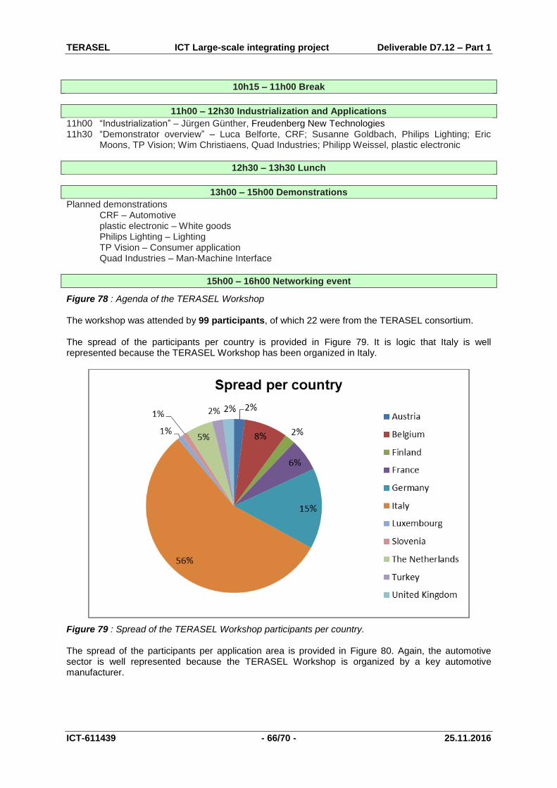
TERASEL ICT Large-scale integrating project Deliverable D7.12 – Part 1
ICT-611439 - 66/70 - 25.11.2016
10h15 – 11h00 Break
11h00 – 12h30 Industrialization and Applications
11h00 “Industrialization” – Jürgen Günther, Freudenberg New Technologies 11h30 “Demonstrator overview” – Luca Belforte, CRF; Susanne Goldbach, Philips Lighting; Eric
Moons, TP Vision; Wim Christiaens, Quad Industries; Philipp Weissel, plastic electronic
12h30 – 13h30 Lunch
13h00 – 15h00 Demonstrations
Planned demonstrations CRF – Automotive plastic electronic – White goods Philips Lighting – Lighting TP Vision – Consumer application Quad Industries – Man-Machine Interface
15h00 – 16h00 Networking event
Figure 78 : Agenda of the TERASEL Workshop The workshop was attended by 99 participants, of which 22 were from the TERASEL consortium. The spread of the participants per country is provided in Figure 79. It is logic that Italy is well represented because the TERASEL Workshop has been organized in Italy.
Figure 79 : Spread of the TERASEL Workshop participants per country. The spread of the participants per application area is provided in Figure 80. Again, the automotive sector is well represented because the TERASEL Workshop is organized by a key automotive manufacturer.

TERASEL ICT Large-scale integrating project Deliverable D7.12 – Part 1
ICT-611439 - 67/70 - 25.11.2016
Figure 80 : Spread of the TERASEL Workshop participants per application area.
e. TERASEL Newsletters The TERASEL Newsletters have the aim to support the dialog between the TERASEL Consortium and the development communities, which work on similar topics, respectively potential customers. The following reader groups are targeted :
Project partners
European Commission, EC Reviewers, Project Officer
Development community
Potential customers
Interested public So far the dominant way of publishing is by electronic means (pdf-file). The newsletter is available in the download area of the project web page: www.terasel.eu The TERASEL newsletters are published roughly every 9 months. In total 4 Newsletters were generated in the course of the TERASEL project :
Newsletter 1 : Iinforms about all general subjects of the TERASEL project, the objectives, the possible applications, the background and the partners.
Newsletter 2 : Informs about further progress of the TERASEL project, which is now half way its duration of 36 months. This second issue of the TERASEL Newsletter presents some aspects of the project in more detail. Emphasis is on the polymer processing. Also work on 2 end-user applications is presented. Finally, also a short report is provided on a major dissemination effort, namely the Ghent Light Festival 2015.
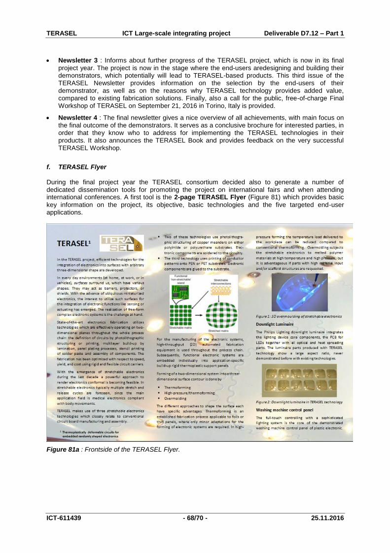
TERASEL ICT Large-scale integrating project Deliverable D7.12 – Part 1
ICT-611439 - 68/70 - 25.11.2016
Newsletter 3 : Informs about further progress of the TERASEL project, which is now in its final project year. The project is now in the stage where the end-users aredesigning and building their demonstrators, which potentially will lead to TERASEL-based products. This third issue of the TERASEL Newsletter provides information on the selection by the end-users of their demonstrator, as well as on the reasons why TERASEL technology provides added value, compared to existing fabrication solutions. Finally, also a call for the public, free-of-charge Final Workshop of TERASEL on September 21, 2016 in Torino, Italy is provided.
Newsletter 4 : The final newsletter gives a nice overview of all achievements, with main focus on the final outcome of the demonstrators. It serves as a conclusive brochure for interested parties, in order that they know who to address for implementing the TERASEL technologies in their products. It also announces the TERASEL Book and provides feedback on the very successful TERASEL Workshop.
f. TERASEL Flyer During the final project year the TERASEL consortium decided also to generate a number of dedicated dissemination tools for promoting the project on international fairs and when attending international conferences. A first tool is the 2-page TERASEL Flyer (Figure 81) which provides basic key information on the project, its objective, basic technologies and the five targeted end-user applications.
Figure 81a : Frontside of the TERASEL Flyer.

TERASEL ICT Large-scale integrating project Deliverable D7.12 – Part 1
ICT-611439 - 69/70 - 25.11.2016
Figure 81b : Backside of the TERASEL Flyer.
g. TERASEL Booklet During the final project year the TERASEL consortium decided also to generate a number of dedicated dissemination tools for promoting the project on international fairs and when attending international conferences. A second tool is the 20-page A5-size TERASEL Booklet which provides more detailed information on the project than the previously described TERASEL Flyer. The Table of Contents of the TERASEL Booklet is as follows : 1. Introduction and motivation
- General - Basic idea / approach - Background on stretchable electronics and thermoplastics
2. Technologies - Stretchable circuit boards with meandering copper : SMI, SCB and SPF : Brief description of the
technology including schematic drawing and pictures of prototypes, as well as design constraints and design rules
- Thermoplastic materials : Joining electronics and thermoplastics - Forming processes : Thermo-forming, High Pressure Forming, injection moulding : Description
of the technology, pictures of the equipment and very brief typical parameters
3. Demonstrators - Glovebox demo (CRF) - Turning knob (Quad) - Ambilight demo(TPVision) - Touch interface (PE) - Powerbalance for lighting (Philips)

TERASEL ICT Large-scale integrating project Deliverable D7.12 – Part 1
ICT-611439 - 70/70 - 25.11.2016
Each demonstrator provides a short description of the use case, a description of the actual demonstrator and the potential of the the TERASEL technology and future application scenario.
4. Prespective
5. Project consortium
h. TERASEL Book The TERASEL consortium will publish in co-operation with River Publishers a book on the TERASEL project. River Publishers is an international publisher that publishes research monographs, professional books, handbooks, edited volumes and journals with focus on key research areas within the fields of Science, Technology and Medicine. The book publication will be intended for graduate level students, researchers and professionals. The book will be available in print and electronic format. In this way, the needs are met of the modern day researcher, student and engineer. As was the case for the TERASEL Workshop, this TERASEL Book was also not foreseen in the Description of Work of TERASEL. The book will cover the results of the TERASEL project, giving people more insights in the technologies and possible applications. It will become a reference book for one time deformable electronic circuits. The table of contents of the book is as follows: 1. Introduction and motivation
2. Technologies for one time deformable circuits - SMI Technology - SCB Technology - SPF Technology - High pressure forming - Thermoforming Technology - Overmoulding Technology
3. Demonstrators - Glovebox demo (CRF) - Turning knob (Quad) - Ambilight demo(TPVision) - Touch interface (PE) - Powerbalance for lighting (Philips)
4. Industrialization of TERASEL technologies
5. Conclusions and Outlook
2. Partner-specific dissemination activities
The following partner-specific activities have been performed during the TERASEL project :
The generation of 8 scientific publications, 3 in Period 1 and 5 in Period 2.
The presentation of 58 scientific/technical presentations at international conferences, 26 in Period 1 and 32 in Period 2.
The presence on 16 international fairs and exhibitions, 4 in Period 1 and 12 in Period 2.
The performing of 36 other dissemination activities (workshops, training, customer visits, etc.), 17 in Period 1 and 19 in Period 2.