ovation i/o reference manual ref 1150 - …ftp.ruigongye.com/200807/ref_1150.pdfref_1150 i contents...
TRANSCRIPT
Ovation I/O Reference Manual REF_1150
November 2005

Copyright Notice
Since the equipment explained in this manual has a variety of uses, the user and those responsible for applying this equipment must satisfy themselves as to the acceptability of each application and use of the equipment. Under no circumstances will Emerson Process Management be responsible or liable for any damage, including indirect or consequential losses resulting from the use, misuse, or application of this equipment.
The text, illustrations, charts, and examples included in this manual are intended solely to explain the use and application of the Ovation® unit. Due to the many variables associated with specific uses or applications, Emerson Process Management cannot assume responsibility or liability for actual use based upon the data provided in this manual.
No patent liability is assumed by Emerson Process Management with respect to the use of circuits, information, equipment, or software described in this manual.
No part of this publication may be reproduced, stored in a retrieval system, or transmitted in any form or by any means, including electronic, mechanical, photocopying, recording or otherwise without the prior express written permission of Emerson Process Management.
The document is the property of and contains Proprietary Information owned by Emerson Process Management and/or its subcontractors and suppliers. It is transmitted in confidence and trust, and the user agrees to treat this document in strict accordance with the terms and conditions of the agreement under which it was provided.
This manual is printed in the USA and is subject to change without notice.
Ovation and WEStation are registered trademarks of Emerson Process Management. All other trademarks or registered trademarks are the property of their respective holders.
Copyright © Emerson Process Management Power & Water Solutions, Inc. All rights reserved.
Emerson Process Management Power & Water Solutions
200 Beta Drive Pittsburgh, PA 15238
USA
E-Mail: [email protected] Website: http://www.EmersonProcess.com
REF_1150 i
Contents
1 Introduction to the Ovation I/O Reference Manual 1 1.1 What is the purpose of the Ovation Input/Output Modules? ............................................... 1 1.2 Description of Terms ........................................................................................................... 2
2 Noise Minimization Techniques 5 2.1 What are the Causes of Electrical Noise? .......................................................................... 5 2.2 Noise Discrimination ........................................................................................................... 6
2.2.1 Energy Level ..................................................................................................... 6 2.3 Noise Sources..................................................................................................................... 8 2.4 Noise Classes ..................................................................................................................... 8 2.5 Noise Rejection ................................................................................................................... 9
2.5.1 What Types of Digital Signal Noise Rejection are Used? ................................. 9 2.6 Analog Signal Shielding Techniques ................................................................................ 12 2.7 What are some Common Input Considerations?.............................................................. 14
2.7.1 4 to 20 mA Signal Considerations................................................................... 14
3 I/O Module General Information 15 3.1 What General Information Should I Know About Ovation I/O Modules? .......................... 15
3.1.1 Ovation Module Features ................................................................................ 16 3.2 What are the I/O Module Types? ...................................................................................... 22
3.2.1 Analog Input Modules...................................................................................... 23 3.2.2 Analog Output Modules................................................................................... 23 3.2.3 Digital Input Modules....................................................................................... 24 3.2.4 Digital Output Modules .................................................................................... 24 3.2.5 Specialty Modules ........................................................................................... 25
3.3 Ovation Module Choices................................................................................................... 25 3.4 Installing Ovation Modules................................................................................................ 29 3.5 Ovation Module Configuration and Status ........................................................................ 30 3.6 Ovation Module Diagnostic LEDs ..................................................................................... 30 3.7 What is Involved in the Replacement of User Serviceable Fuses? .................................. 31
3.7.1 Electronics Module Fuses ............................................................................... 31 3.7.2 Personality Module Fuses............................................................................... 31 3.7.3 Ovation Cabinet Fuses.................................................................................... 33
Table of Contents
ii REF_1150
3.8 Personality Module Jumpers.............................................................................................33 3.9 I/O Environmental Specifications ......................................................................................34
4 Analog Input Module (13 bits) 37 4.1 Description ........................................................................................................................ 37 4.2 Module Group Information ................................................................................................37
4.2.1 Electronics Modules (Emods).......................................................................... 37 4.2.2 Personality Modules (Pmods) ......................................................................... 38 4.2.3 Subsystems, Analog Input (13 Bit) .................................................................. 38
4.3 Module Specific Information.............................................................................................. 39 4.3.1 External Power Supplies ................................................................................. 39 4.3.2 Thermocouple Function................................................................................... 40
4.4 Wiring Information .............................................................................................................44 4.4.1 13-Bit Analog Input Terminal Block Wiring Information .................................. 44 4.4.2 13-Bit Analog Input Field Connection Wiring Diagrams (Non-CE Mark Certified) 46 4.4.3 13-Bit Analog Input Field Connection Wiring Diagrams (CE Mark Certified).. 47
4.5 Address Location Information ........................................................................................... 48 4.5.1 Configuration and Status Register .................................................................. 48
4.6 Diagnostic LEDs................................................................................................................52 4.7 Specifications .................................................................................................................... 53
5 Analog Input Module (14 bits) 55 5.1 Description ........................................................................................................................ 55 5.2 Module Group Information ................................................................................................55
5.2.1 Electronics Modules (Emods).......................................................................... 55 5.2.2 Personality Modules (Pmods) ......................................................................... 55 5.2.3 Subsystems, Analog Input (14 Bit) .................................................................. 56
5.3 Module Specific Information.............................................................................................. 56 5.3.1 Module Block Diagram ....................................................................................56 5.3.2 External Power Supplies ................................................................................. 57
5.4 Wiring Information .............................................................................................................57 5.4.1 14-Bit Analog Input Terminal Block Wiring Information .................................. 57 5.4.2 14-Bit Analog Input Field Connection Wiring Diagrams (Non-CE Mark Certified) 59 5.4.3 14-Bit Analog Input Field Connection Wiring Diagrams (CE Mark Certified).. 60
5.5 Address Location Information ........................................................................................... 60 5.5.1 Configuration and Status Register .................................................................. 60
5.6 Diagnostic LEDs................................................................................................................63 5.7 Specifications .................................................................................................................... 64
6 Analog High Speed Input Module (14 bits) 67 6.1 Description ........................................................................................................................ 67 6.2 Module Group Information ................................................................................................67
6.2.1 Electronics Module (Emod) ............................................................................. 67 6.2.2 Personality Module (Pmod) ............................................................................. 68

Table of Contents
REF_1150 iii
6.2.3 Subsystems, Analog Input (14 bit High Speed) .............................................. 68 6.3 Module Specific Information.............................................................................................. 69
6.3.1 Module Block Diagram ....................................................................................69 6.3.2 External Power Supplies ................................................................................. 69 6.3.3 Thermocouple Function................................................................................... 70
6.4 Wiring Information .............................................................................................................74 6.4.1 High Speed Analog Input Terminal Block Wiring Information - Pmod 1C31227 74 6.4.2 High Speed Analog Input Terminal Block Wiring Information - Pmod 1C31116 76 6.4.3 High Speed Analog Input Field Connection Wiring Diagrams ........................ 77 6.4.4 Non-CE Mark Systems.................................................................................... 78 6.4.5 CE Mark Systems............................................................................................ 79 6.4.6 Non-CE Mark Certified Systems ..................................................................... 80 6.4.7 CE Mark Certified Systems ............................................................................. 81
6.5 Address Location Information ........................................................................................... 82 6.5.1 High Speed Analog Input Address Locations (Group 1) ................................. 82 6.5.2 High Speed Analog Input Address Locations (Group 2) ................................. 84 6.5.3 High Speed Analog Input Address Locations (Group 3) ................................. 86 6.5.4 High Speed Analog Input Address Locations (Group 4) ................................. 88
6.6 Diagnostic LEDs................................................................................................................91 6.7 Specifications .................................................................................................................... 92
7 Analog Output Module 93 7.1 Description ........................................................................................................................ 93 7.2 Module Group Information ................................................................................................93
7.2.1 Electronics Modules (Emods).......................................................................... 93 7.2.2 Personality Module (Pmod) ............................................................................. 93 7.2.3 Subsystems, Analog Output............................................................................ 94
7.3 Wiring Information .............................................................................................................94 7.3.1 Analog Output Terminal Block Wiring Information .......................................... 94 7.3.2 Analog Output Field Connection Wiring Diagrams (Non-CE Mark Certified).. 95 7.3.3 Analog Output Field Connection Wiring Diagrams (CE Mark Certified).......... 96
7.4 Address Location Information ........................................................................................... 96 7.4.1 Configuration and Status Register .................................................................. 96 7.4.2 Output Current Status Register ....................................................................... 98
7.5 Diagnostic LEDs................................................................................................................98 7.6 Specifications .................................................................................................................... 99
8 Contact Input Module 101 8.1 Description ...................................................................................................................... 102 8.2 Module Group Information ..............................................................................................102
8.2.1 Electronics Module (Emod) ........................................................................... 102 8.2.2 Personality Module (Pmod) ........................................................................... 102 8.2.3 Subsystems, Contact Input ........................................................................... 103
8.3 Wiring Information ...........................................................................................................103 8.3.1 Contact Input Terminal Block Wiring Information.......................................... 103 8.3.2 Field Wiring Restrictions:...............................................................................104 8.3.3 Field Wiring Cable Lengths ........................................................................... 104

Table of Contents
iv REF_1150
8.3.4 Contact Input Front End Field Connection Wiring Diagrams ........................ 105 8.3.5 Contact Input Cable Impedances in Field Wiring.......................................... 106
8.4 Address Location Information ......................................................................................... 109 8.4.1 Configuration and Status Register ................................................................ 109
8.5 Diagnostic LEDs..............................................................................................................110 8.6 Specifications .................................................................................................................. 111
9 Compact Contact Input Module 113 9.1 Description ...................................................................................................................... 114 9.2 Module Group Information ..............................................................................................114
9.2.1 Electronics Module (Emod) ........................................................................... 114 9.2.2 Foam Insert ...................................................................................................115 9.2.3 Subsystems, Compact Contact Input............................................................115
9.3 Wiring Information ...........................................................................................................115 9.3.1 Compact Contact Input Terminal Block Wiring Information .......................... 115 9.3.2 Field Wiring Restrictions:...............................................................................116 9.3.3 Field Wiring Cable Lengths ........................................................................... 116 9.3.4 Compact Contact Input Front End Field Connection Wiring Diagrams......... 118 9.3.5 Compact Contact Input Cable Impedances in Field Wiring .......................... 119
9.4 Address Location Information ......................................................................................... 122 9.4.1 Configuration and Status Register ................................................................ 122
9.5 Diagnostic LEDs..............................................................................................................123 9.6 Specifications .................................................................................................................. 124
10 Digital Input Module 125 10.1 Description ...................................................................................................................... 125 10.2 Module Group Information ..............................................................................................125
10.2.1 Electronics Modules (Emods)........................................................................125 10.2.2 Personality Modules (Pmods) .......................................................................126 10.2.3 Subsystems, Digital Input..............................................................................126
10.3 Module Specific Information............................................................................................ 127 10.3.1 External Power Supplies - Single-Ended Digital Input Front End ................. 127 10.3.2 External Power Supplies - Differential Digital Input Front End...................... 128
10.4 Wiring Information ...........................................................................................................129 10.4.1 Digital Input Terminal Block Wiring Information ............................................ 129 10.4.2 Field Wiring Considerations for the Digital Input Configuration .................... 130 10.4.3 Non-CE Mark Certified Systems ...................................................................131 10.4.4 CE Mark Certified Systems ...........................................................................132
10.5 Address Location Information ......................................................................................... 133 10.5.1 Configuration and Status Register ................................................................ 133
Table of Contents
REF_1150 v
10.6 Diagnostic LEDs..............................................................................................................134 10.7 Specifications .................................................................................................................. 135
11 Compact Digital Input Module 137 11.1 Description ...................................................................................................................... 137 11.2 Module Group Information ..............................................................................................138
11.2.1 Electronics Modules (Emods)........................................................................138 11.2.2 Personality Module (Pmod) ........................................................................... 138 11.2.3 Foam Insert ...................................................................................................138 11.2.4 Subsystems, Compact Digital Input ..............................................................138
11.3 Module Specific Information............................................................................................ 139 11.3.1 External Power Supplies ...............................................................................139
11.4 Wiring Information ...........................................................................................................139 11.4.1 Compact Digital Input Terminal Block Wiring Information............................. 139 11.4.2 Field Wiring Considerations for the Single-Ended Compact Digital Input Front End 141 11.4.3 Field Wiring Considerations for the Differential Compact Digital Input Front End 142 11.4.4 Field Wiring Considerations for the 16 Individually Fused Compact Digital Input Front End ...............................................................................................................143 11.4.5 Non-CE Mark Certified System .....................................................................145 11.4.6 CE Mark Certified System.............................................................................146
11.5 Address Location Information ......................................................................................... 147 11.5.1 Configuration and Status Register ................................................................ 147
11.6 Diagnostic LEDs..............................................................................................................148 11.7 Specifications .................................................................................................................. 149
12 Digital Output Module 151 12.1 Description ...................................................................................................................... 151 12.2 Module Group Information ..............................................................................................151
12.2.1 Electronics Module (Emod) ........................................................................... 151 12.2.2 Personality Modules (Pmods) .......................................................................152 12.2.3 Subsystems, Digital Output ...........................................................................152
12.3 Module Specific Information............................................................................................ 153 12.3.1 External Power Supplies ...............................................................................153 12.3.2 Relay Panels .................................................................................................153 12.3.3 Blown Fuse Detection Circuit ........................................................................164
12.4 Wiring Information ...........................................................................................................164 12.4.1 Digital Output Terminal Block Wiring Information ......................................... 164 12.4.2 Digital Output Field Connection Wiring Diagrams......................................... 166 12.4.3 Relay Panel Application Diagrams................................................................ 171
12.5 Address Location Information ......................................................................................... 173 12.5.1 Digital Output Address Locations..................................................................173

Table of Contents
vi REF_1150
12.6 Diagnostic LEDs..............................................................................................................175 12.7 Specifications .................................................................................................................. 175
13 HART Analog Input Module 177 13.1 Description ...................................................................................................................... 177 13.2 Module Group Information ..............................................................................................177
13.2.1 Electronics Module (Emod) ........................................................................... 177 13.2.2 Personality Module (Pmod) ........................................................................... 178 13.2.3 Subsystems, HART Analog Input (16 Bit) .....................................................178
13.3 Module Specific Information............................................................................................ 179 13.3.1 Module Block Diagram ..................................................................................179 13.3.2 External Power Supplies ...............................................................................181
13.4 Wiring Information ...........................................................................................................182 13.4.1 HART Analog Input Terminal Block Wiring Information ................................ 182 13.4.2 HART Analog Input Field Connection Wiring Diagrams (Non-CE Mark Certified Systems) 183 13.4.3 HART Analog Input Field Connection Wiring Diagrams (CE Mark Certified Systems) 184 13.4.4 Field Wiring Cable Requirements ................................................................. 185
13.5 Address Location Information ......................................................................................... 188 13.5.1 Configuration and Status Register ................................................................ 188 13.5.2 HART Analog Input Enable Register (Address 14 or E in Hex) .................... 190
13.6 Diagnostic LEDs..............................................................................................................191 13.7 Specifications .................................................................................................................. 192
14 HART High Performance Analog Input Module 193 14.1 Description ...................................................................................................................... 193 14.2 Module Group Information ..............................................................................................194
14.2.1 Personality Module (Pmod) ........................................................................... 194 14.2.2 Electronics Module (Emod) ........................................................................... 194 14.2.3 Subsystems, HART HP Analog Input (16 Bit) ............................................... 194
14.3 Module Specific Information............................................................................................ 195 14.3.1 Module Block Diagram and Field Connection Wiring Diagram..................... 195
15 HART H. P. Analog Input Subsystem Block Diagram Error! Bookmark not defined.
15.1.1 External Power Supplies ...............................................................................197 15.2 Wiring Information ...........................................................................................................198
15.2.1 HART HP Analog Input Personality Module Information .............................. 198 15.2.2 HART HP Analog Input Terminal Block Wiring Information .......................... 198 15.2.3 Field Wiring Cable Requirements ................................................................. 199
15.3 Address Location Information ......................................................................................... 200 15.3.1 HART HP Analog Input Address Locations................................................... 200

Table of Contents
REF_1150 vii
15.4 Diagnostic LEDs..............................................................................................................204 15.5 Specifications .................................................................................................................. 205
16 HART Analog Output Module 207 16.1 Description ...................................................................................................................... 207 16.2 Module Group Information ..............................................................................................207
16.2.1 Electronics Module (Emod) ........................................................................... 207 16.2.2 Personality Module (Pmod) ........................................................................... 207 16.2.3 Subsystems, HART Analog Output (14 Bit) .................................................. 208
16.3 Module Specific Information............................................................................................ 209 16.3.1 Module Block Diagrams ................................................................................209 16.3.2 External Power Supplies ...............................................................................210
16.4 Wiring Information ...........................................................................................................211 16.4.1 HART Analog Output Terminal Block Wiring Information ............................. 211 16.4.2 HART Analog Output Field Connection Wiring Diagrams (Non-CE Mark Certified Systems)...........................................................................................................212 16.4.3 HART Analog Output Field Connection Wiring Diagrams (CE Mark Certified Systems) 213 16.4.4 Field Wiring Cable Requirements ................................................................. 213
16.5 Address Location Information ......................................................................................... 214 16.5.1 Configuration and Status Register ................................................................ 214 16.5.2 Open Loop Detect Register........................................................................... 217
16.6 Diagnostic LEDs..............................................................................................................219 16.7 Specifications .................................................................................................................. 220
17 HART High Performance Analog Output Module 223 17.1 Description ...................................................................................................................... 223 17.2 Module Group Information ..............................................................................................223
17.2.1 Electronics Module (Emod) ........................................................................... 223 17.2.2 Subsystems, HART Analog Output (16 Bit) .................................................. 223
17.3 Module Specific Information............................................................................................ 225 17.3.1 Module Block Diagrams ................................................................................225
17.4 Wiring Information ...........................................................................................................226 17.4.1 Output Terminal Block Wiring Information .................................................... 226 17.4.2 HART H.P. Analog Output Field Wiring Connections with Personality Module Foam Cavity Insert (Non-CE Mark Certified System) .....................................................228 17.4.3 HART H. P. Analog Output Field Wiring Connections with Personality Module (Non-CE Mark Certified System) ....................................................................................228 17.4.4 Field Wiring Cable Requirements ................................................................. 229
17.5 Address Location Information ......................................................................................... 229 17.5.1 HART High Performance Analog Output Module Registers ......................... 229

Table of Contents
viii REF_1150
17.6 Diagnostic LEDs..............................................................................................................233 17.7 Specifications .................................................................................................................. 234
18 Link Controller (LC) Module 235 18.1 Description ...................................................................................................................... 235 18.2 Module Group Information ..............................................................................................235
18.2.1 Electronics Module (Emod) ........................................................................... 235 18.2.2 Personality Modules (Pmods) .......................................................................235 18.2.3 Subsystems, Link Controller..........................................................................236
19 Loop Interface Module 237 19.1 Description ...................................................................................................................... 237 19.2 Module Group Information ..............................................................................................238
19.2.1 Module Groups..............................................................................................238 19.2.2 Electronic Modules (Emods) ......................................................................... 238 19.2.3 Personality Modules (Pmods) .......................................................................238 19.2.4 Subsystems, Loop Interface..........................................................................239
19.3 Module Specific Information............................................................................................ 241 19.3.1 Modes of Operation....................................................................................... 241 19.3.2 Manual Station Control..................................................................................241 19.3.3 Normal and Inverse Analog Output...............................................................242 19.3.4 External Power Supplies ...............................................................................242
19.4 Wiring Information ...........................................................................................................243 19.4.1 Loop Interface Terminal Block Wiring Information ........................................ 243 19.4.2 Loop Interface Field Connection Wiring Diagrams ....................................... 246 19.4.3 SLIM Serial Port Connector........................................................................... 259
19.5 Address Location Information ......................................................................................... 260 19.5.1 Configuration and Status Register ................................................................ 260 19.5.2 Secondary Configuration and Status Register .............................................. 261 19.5.3 Point Quality Register....................................................................................262
19.6 Diagnostic LEDs..............................................................................................................262 19.7 Specifications .................................................................................................................. 264
20 Pulse Accumulator Module 269 20.1 Description ...................................................................................................................... 269 20.2 Module Group Information ..............................................................................................269
20.2.1 Electronics Modules (Emods)........................................................................269 20.2.2 Personality Modules (Pmods) .......................................................................270
20.3 Wiring Information ...........................................................................................................271 20.3.1 Pulse Accumulator Terminal Block Wiring Information ................................. 271 20.3.2 Pulse Accumulator Field Connection Wiring Diagrams (Non-CE Mark Certified) 273 20.3.3 Pulse Accumulator Field Connection Wiring Diagrams (CE Mark Certified) 278
20.4 Address Location Information ......................................................................................... 281 20.4.1 Configuration and Status Register ................................................................ 281 20.4.2 Secondary Configuration and Status Register .............................................. 284
Table of Contents
REF_1150 ix
20.5 Diagnostic LEDs..............................................................................................................286 20.6 Specifications .................................................................................................................. 286
20.6.1 Input Signal Levels ........................................................................................288
21 Relay Output Module 291 21.1 Description ...................................................................................................................... 291 21.2 Module Group Information ..............................................................................................291
21.2.1 Electronic Module (Emod) .............................................................................291 21.3 Module Specific Information............................................................................................ 293
21.3.1 External Power Supplies ...............................................................................293 21.3.2 Using Relay Output Bases ............................................................................ 294 21.3.3 Blown Fuse Detection Circuit ........................................................................295
21.4 Wiring Information ...........................................................................................................295 21.4.1 Relay Output Terminal Block Wiring Information .......................................... 295 21.4.2 Relay Output Terminal Block Wiring Information .......................................... 297 21.4.3 Relay Output Field Connection Wiring Diagrams (Non-CE Mark Certified).. 299 21.4.4 Relay Output Field Connection Wiring Diagrams (CE Mark Certified).......... 300
21.5 Address Location Information ......................................................................................... 301 21.5.1 Configuration and Status Register ................................................................ 301
21.6 Diagnostic LEDs..............................................................................................................302 21.7 Specifications .................................................................................................................. 303
22 RTD Module (4 Channel) 305 22.1 Description ...................................................................................................................... 305 22.2 Module Group Information ..............................................................................................305
22.2.1 Electronics Modules (Emods)........................................................................305 22.2.2 Personality Modules (Pmods) .......................................................................305 22.2.3 Subsystems, RTD Module.............................................................................306
22.3 Wiring Information ...........................................................................................................306 22.3.1 RTD (4 Channel) Systems (Using Pmod 1C31164G0) Terminal Block Wiring Information ...................................................................................................................... 306 22.3.2 RTD (4 Channel) Systems (Using Pmod 1C31164G02) Terminal Block Wiring Information ...................................................................................................................... 307 22.3.3 Systems Using Personality Module 1C31164G01 ........................................ 308 22.3.4 Non-CE Mark Systems Using Personality Module 1C31164G02 ................. 309 22.3.5 CE Mark Certified Systems Using Personality Module 1C31164G02........... 310
22.4 Address Location Information ......................................................................................... 311 22.4.1 Configuration and Status Register ................................................................ 311
22.5 Diagnostic LEDs..............................................................................................................313 22.6 Specifications .................................................................................................................. 313
22.6.1 RTD Ranges..................................................................................................314
23 RTD Module (8 Channel) 317 23.1 Description ...................................................................................................................... 317 23.2 Module Group Information ..............................................................................................318
23.2.1 Electronics Module (Emod) ........................................................................... 318 23.2.2 Personality Module (Pmod) ........................................................................... 318
Table of Contents
x REF_1150
23.2.3 Subsystems, 8-Channel RTD Module........................................................... 318 23.3 Wiring Information ...........................................................................................................318
23.3.1 RTD (8 Channel) Systems (Using Pmod 5X00121G01) Terminal Block Wiring Information ...................................................................................................................... 318 23.3.2 Module and Field Connection Wiring ............................................................319 23.3.3 Module Block Diagram and Field Connection Wiring Diagram..................... 321
23.4 Address Location Information ......................................................................................... 322 23.4.1 Configuration and Status Register ................................................................ 322 23.4.2 Channel Scale Configuration Registers ........................................................ 323
23.5 Diagnostic LEDs..............................................................................................................325 23.6 Specifications .................................................................................................................. 325
23.6.1 8-Channel RTD Ranges ................................................................................326
24 Sequence of Events Module 329 24.1 Description ...................................................................................................................... 330 24.2 Module Group Information ..............................................................................................331
24.2.1 Electronics Modules (Emods)........................................................................331 24.2.2 Personality Modules (Pmods) .......................................................................331 24.2.3 Subsystems, Sequence of Events ................................................................ 331
24.3 Module Specific Information............................................................................................ 331 24.3.1 External Power Supplies ...............................................................................331
24.4 Wiring Information, Sequence of Events Modules.......................................................... 332 24.4.1 Sequence of Events Digital Input Field Interface Modules ........................... 332 24.4.2 Sequence of Events Contact Field Interface Modules .................................. 340
24.5 Address Location Information ......................................................................................... 347 24.5.1 Sequence of Events Contact Input Configuration and Status Register ........ 347
24.6 Diagnostic LEDs..............................................................................................................348 24.7 Specifications .................................................................................................................. 348
25 Compact Sequence of Events Module 351 25.1 Description ...................................................................................................................... 352 25.2 Module Group Information ..............................................................................................353
25.2.1 Electronics Modules (Emods)........................................................................353 25.3 Module Specific Information............................................................................................ 354
25.3.1 External Power Supplies ...............................................................................354 25.4 Wiring Information, Sequence of Events Modules.......................................................... 355
25.4.1 Sequence of Events Digital Input Field Interface Modules ........................... 355 25.4.2 Sequence of Events Contact Field Interface Modules .................................. 364
25.5 Diagnostic LEDs..............................................................................................................371 25.6 Specifications .................................................................................................................. 371
26 Servo Driver Module 373 26.1 Description ...................................................................................................................... 373 26.2 Operation......................................................................................................................... 374
26.2.1 AD/DA Conversion and Timing .....................................................................374
Table of Contents
REF_1150 xi
26.3 Module Groups................................................................................................................375 26.3.1 Electronics Modules (Emods)........................................................................375 26.3.2 Personality Modules (Pmods) .......................................................................375 26.3.3 Subsystems, Servo Driver.............................................................................375
26.4 Module Specific Information............................................................................................ 376 26.4.1 Servo Driver Modes.......................................................................................376 26.4.2 Using the Serial Port for Calibration, Settings............................................... 379 26.4.3 Using the Serial Port for Calibration, Connections........................................ 379 26.4.4 Performing Calibration................................................................................... 380 26.4.5 Valve Position Control ................................................................................... 384 26.4.6 Controller Interface........................................................................................386 26.4.7 Servo Driver Commands ...............................................................................389
26.5 Wiring Information ...........................................................................................................394 26.5.1 Servo Driver Terminal Block Wiring Information ........................................... 394 26.5.2 Servo Driver Field Connection Wiring Diagrams........................................... 396
26.6 Address Location Information ......................................................................................... 399 26.6.1 Configuration and Status Register ................................................................ 399 26.6.2 Severe Errors Status Register....................................................................... 401
26.7 Diagnostics...................................................................................................................... 403 26.7.1 EPROM Checksum Error .............................................................................. 403
26.8 Diagnostic LEDs..............................................................................................................404 26.9 Specifications .................................................................................................................. 405
27 SLIM (Small Loop Interface Module) 407 27.1 Description ...................................................................................................................... 408 27.2 Module Specific Information............................................................................................ 409
27.2.1 Features ........................................................................................................409 27.2.2 Groups and Modes........................................................................................409
27.3 Wiring Information ...........................................................................................................413 27.3.1 Wiring ............................................................................................................413
27.4 Specifications .................................................................................................................. 414
28 Speed Detector Module 415 28.1 Description ...................................................................................................................... 415 28.2 Module Group Information ..............................................................................................415
28.2.1 Electronics Module (Emod) ........................................................................... 415 28.2.2 Personality Module (Pmod) ........................................................................... 415 28.2.3 Subsystems, Speed Detector........................................................................416
28.3 Wiring Information ...........................................................................................................417 28.3.1 Speed Detector Terminal Block Wiring Information ...................................... 417 28.3.2 Speed Detector Field Connection Wiring Diagrams ..................................... 418
28.4 Address Location Information ......................................................................................... 420 28.4.1 Configuration and Status Register ................................................................ 420
Table of Contents
xii REF_1150
28.5 Diagnostic LEDs..............................................................................................................422 28.6 Specifications .................................................................................................................. 422
29 Valve Positioner Module 425 29.1 Descriptions .................................................................................................................... 426
29.1.1 Description for Single VP Module .................................................................426 29.2 Module Group Information ..............................................................................................429
29.2.1 Electronic Modules (Emods) ......................................................................... 429 29.2.2 Personality Modules (Pmods) .......................................................................430
29.3 Module Specific Information............................................................................................ 432 29.3.1 Firmware Levels ............................................................................................432 29.3.2 Primary/Backup Status Transitions ............................................................... 433 29.3.3 Valve Positioner Modes.................................................................................434 29.3.4 Controller Interface........................................................................................438 29.3.5 Configuration Commands.............................................................................. 442 29.3.6 SLIM (Small Loop Interface Module) Interface.............................................. 447 29.3.7 Valve Positioner Control................................................................................ 449
29.4 Calibration ....................................................................................................................... 451 29.4.1 Performing Calibration Using the Serial Port ................................................ 451 29.4.2 Performing Calibration Using a Graphic........................................................ 455 29.4.3 Performing Redundant VP Calibration .......................................................... 459
29.5 Wiring Information ...........................................................................................................460 29.5.1 Valve Positioner Terminal Block Wiring Information ..................................... 460 29.5.2 Valve Positioner Field Connection Wiring Diagram (Non-CE Mark) ............. 462 29.5.3 Valve Positioner Field Connection Wiring Diagram (CE Mark)..................... 466 29.5.4 Swapping Connections to Affect the Output .................................................469
29.6 SLIM Serial Port Connector ............................................................................................ 469 29.7 Address Location Information ......................................................................................... 470
29.7.1 Configuration and Status Register ................................................................ 470 29.7.2 Secondary Configuration and Status Register .............................................. 471
29.8 Diagnostics...................................................................................................................... 472 29.8.1 DA Readback Error .......................................................................................472
29.9 Troubleshooting .............................................................................................................. 474 29.9.1 Online VP Replacement ................................................................................474 29.9.2 Demodulator Gain .........................................................................................475 29.9.3 LVDT Wiring Problems (6-wire LVDT) ..........................................................476 29.9.4 Servo Wiring Problems.................................................................................. 477
29.10 Diagnostic LEDs..............................................................................................................477 29.11 Specifications .................................................................................................................. 478
30 Ovation Local I/O 481 30.1 Description ...................................................................................................................... 481 30.2 Local I/O Features...........................................................................................................482 30.3 Controller Cabinet Components (Local I/O).................................................................... 482
30.3.1 Controller Cabinet Components and Cabling (local I/O)............................... 484 30.3.2 Controller Backplane (CBO)..........................................................................485

Table of Contents
REF_1150 xiii
30.4 Extended I/O Cabinet Components ................................................................................486 30.5 Cabinet Components (Controller and Extended Cabinet) .............................................. 488 30.6 General Requirements for I/O Cable ..............................................................................491
30.6.1 Local I/O Communications Cable (5A26141)................................................ 491 30.6.2 Selecting the IOIC (PCI) Cards .....................................................................491
30.7 Local I/O Status LEDs.....................................................................................................491 30.7.1 LEDs for PCQL Card.....................................................................................492 30.7.2 LEDs for PCRL Card .....................................................................................492
31 Ovation Remote I/O 495 31.1 Description ...................................................................................................................... 495 31.2 Remote I/O Features....................................................................................................... 496 31.3 Controller Cabinet Components (Remote I/O)................................................................496
31.3.1 Controller Cabinet Components and Cabling (local and remote I/O)............ 499 31.3.2 Controller Backplane (CBO)..........................................................................500 31.3.3 MAU with Typical Fiber-Optic Connector Pairs............................................. 501 31.3.4 Example of Typical MAU Cable Connections to Remote Nodes .................. 502
31.4 Remote Node Cabinet Components ............................................................................... 503 31.4.1 Typical Remote Node Cabinet ......................................................................505 31.4.2 Remote Node Controller (RNC) .................................................................... 506 31.4.3 Remote Node Transition Panel (TND) ..........................................................506
31.5 Extended I/O Cabinet Components ................................................................................507 31.5.1 Cabinet Components (Controller, Remote Node, and Extended Cabinet) ... 509 31.5.2 Ovation Standard I/O Modules and Base Units ............................................ 510 31.5.3 Relay Output Modules and Bases.................................................................511 31.5.4 I/O Dual Branch Transition Panel (ROP) ...................................................... 512 31.5.5 Ovation I/O Single Branch Transition Panels................................................ 513
31.6 General Requirements for I/O Cable ..............................................................................513 31.6.1 I/O Communications Cable (5A26141) ......................................................... 513
31.7 Configuring Remote I/O Cabinets ...................................................................................514 31.7.1 Placing the MAU Module...............................................................................514
31.8 Diagnostic LEDs..............................................................................................................518 31.8.1 LEDs for PCRR Card ....................................................................................519
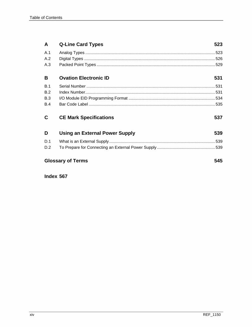
Table of Contents
xiv REF_1150
A Q-Line Card Types 523 A.1 Analog Types ..................................................................................................................523 A.2 Digital Types ................................................................................................................... 526 A.3 Packed Point Types ........................................................................................................529
B Ovation Electronic ID 531 B.1 Serial Number ................................................................................................................. 531 B.2 Index Number..................................................................................................................531 B.3 I/O Module EID Programming Format ............................................................................ 534 B.4 Bar Code Label ...............................................................................................................535
C CE Mark Specifications 537
D Using an External Power Supply 539 D.1 What is an External Supply .............................................................................................539 D.2 To Prepare for Connecting an External Power Supply ................................................... 539
Glossary of Terms 545
Index 567
REF_1150 1
IN THIS SECTION
What is the purpose of the Ovation Input/Output Modules? ...............................................1 Description of Terms ...........................................................................................................2
1.1 WHAT IS THE PURPOSE OF THE OVATION INPUT/OUTPUT MODULES?
The Ovation Distributed Control System provides modulating control, sequential control, and data acquisition for a variety of system applications. This system consists of a configurable mix of functional Input/Output (I/O) modules that communicate on the I/O bus to the Ovation Controller.
I/O modules provide an interface between the Ovation Controller and the processes in the plant. Ovation I/O modules are “plug-in” components with built-in fault tolerance and diagnostics. They are able to operate on a wide range of signals and perform a multitude of functions.
The Ovation I/O modules are locked into base units. These base units are housed in the Controller cabinets where they are mounted on DIN rails and wired to the appropriate field devices.
The standard modular components typically consist of the following:
Electronics module (Emod) Personality module (Pmod) Base Unit (containing the field terminations)
The relay output modular components consist of the following:
Electronics module Base Unit (containing the field terminations)
The following information describes the I/O modules and their usage in the Ovation system.
Detailed information about Ovation cabinets can be found in the applicable Planning book. (See Planning and Installing Your Ovation System.)
S E C T I O N 1
INTRODUCTION TO THE OVATION I/O REFERENCE MANUAL
1.2 Description of Terms
2 REF_1150
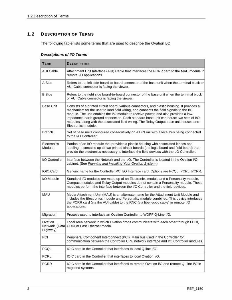
1.2 DESCRIPTION OF TERMS
The following table lists some terms that are used to describe the Ovation I/O.
Descriptions of I/O Terms
TE RM DE S C RI P T I O N
AUI Cable Attachment Unit Interface (AUI) Cable that interfaces the PCRR card to the MAU module in remote I/O applications.
A Side Refers to the left side board-to-board connector of the base unit when the terminal block or AUI Cable connector is facing the viewer.
B Side Refers to the right side board-to-board connector of the base unit when the terminal block or AUI Cable connector is facing the viewer.
Base Unit Consists of a printed circuit board, various connectors, and plastic housing. It provides a mechanism for the user to land field wiring, and connects the field signals to the I/O module. The unit enables the I/O module to receive power, and also provides a low-impedance earth ground connection. Each standard base unit can house two sets of I/O modules, along with the associated field wiring. The Relay Output base unit houses one Electronics module.
Branch Set of base units configured consecutively on a DIN rail with a local bus being connected to the I/O Controller.
Electronics Module
Portion of an I/O module that provides a plastic housing with associated lenses and labeling. It contains up to two printed circuit boards (the logic board and field board) that provide the electronics necessary to interface the field devices with the I/O Controller.
I/O Controller Interface between the Network and the I/O. The Controller is located in the Ovation I/O cabinet. (See Planning and Installing Your Ovation System.)
IOIC Card Generic name for the Controller PCI I/O Interface card. Options are PCQL, PCRL, PCRR.
I/O Module Standard I/O modules are made up of an Electronics module and a Personality module. Compact modules and Relay Output modules do not contain a Personality module. These modules perform the interface between the I/O Controller and the field devices.
MAU Media Attachment Unit (MAU) is an alternate name for the Attachment Unit Module and includes the Electronics module and Personality module combined. This device interfaces the PCRR card (via the AUI cable) to the RNC (via fiber-optic cable) in remote I/O applications.
Migration Process used to interface an Ovation Controller to WDPF Q-Line I/O.
Ovation Network (Data Highway)
Local area network in which Ovation drops communicate with each other through FDDI, CDDI or Fast Ethernet media.
PCI Peripheral Component Interconnect (PCI). Main bus used in the Controller for communication between the Controller CPU network interface and I/O Controller modules.
PCQL IOIC card in the Controller that interfaces to local Q-line I/O.
PCRL IOIC card in the Controller that interfaces to local Ovation I/O.
PCRR IOIC card in the Controller that interfaces to remote Ovation I/O and remote Q-Line I/O in migrated systems.
1.2 Description of Terms
REF_1150 3
TE RM DE S C RI P T I O N
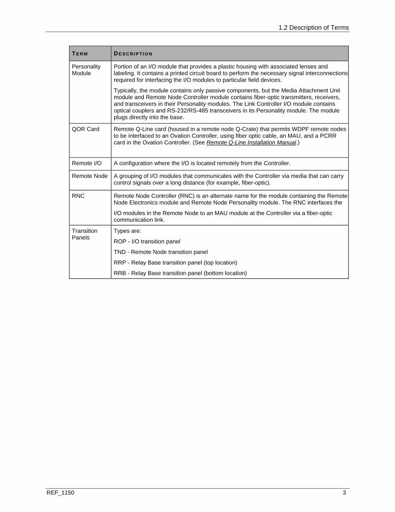
Personality Module
Portion of an I/O module that provides a plastic housing with associated lenses and labeling. It contains a printed circuit board to perform the necessary signal interconnections required for interfacing the I/O modules to particular field devices.
Typically, the module contains only passive components, but the Media Attachment Unit module and Remote Node Controller module contains fiber-optic transmitters, receivers, and transceivers in their Personality modules. The Link Controller I/O module contains optical couplers and RS-232/RS-485 transceivers in its Personality module. The module plugs directly into the base.
QOR Card Remote Q-Line card (housed in a remote node Q-Crate) that permits WDPF remote nodes to be interfaced to an Ovation Controller, using fiber optic cable, an MAU, and a PCRR card in the Ovation Controller. (See Remote Q-Line Installation Manual.)
Remote I/O A configuration where the I/O is located remotely from the Controller.
Remote Node A grouping of I/O modules that communicates with the Controller via media that can carry control signals over a long distance (for example, fiber-optic).
RNC Remote Node Controller (RNC) is an alternate name for the module containing the Remote Node Electronics module and Remote Node Personality module. The RNC interfaces the
I/O modules in the Remote Node to an MAU module at the Controller via a fiber-optic communication link.
Transition Panels
Types are:
ROP - I/O transition panel
TND - Remote Node transition panel
RRP - Relay Base transition panel (top location)
RRB - Relay Base transition panel (bottom location)

REF_1150 5
IN THIS SECTION
What are the Causes of Electrical Noise? .......................................................................... 5 Noise Discrimination ........................................................................................................... 6 Noise Sources..................................................................................................................... 8 Noise Classes ..................................................................................................................... 8 Noise Rejection ................................................................................................................... 9 Analog Signal Shielding Techniques ................................................................................12 What are some Common Input Considerations?..............................................................14
2.1 WHAT ARE THE CAUSES OF ELECTRICAL NOISE?
A wide variety of analog and/or digital circuits are associated with the Ovation System’s installation. There are low-level voltage circuits, high-level voltage circuits, circuits that transfer information, and circuits that transfer power. These circuits are placed into two categories: noise-producing circuits and noise-sensitive circuits.
Noise problems typically occur when transmitting analog (voltage, current, and other measured values) or digital information (on/off conditions, pulse trains or similar data) via inter-connected or wired circuits. The information carried by signals in such circuits may become distorted during transfer and errors may result from this distortion.
The difference between the signal of transmitted information and the signal of that information as received is called noise (see the figures in Energy Level (see page 6) and Frequency (see page 7)). The noise minimization techniques briefly described in this section focus on preventing errors by either eliminating the noise, or when elimination is not possible, performing steps to lessen its impact.
The following topics discuss the causes of electrical noise in your Ovation system and the recommended techniques for eliminating or reducing that noise.
Noise Discrimination (see page 6). Noise Sources (see page 7). Noise Classes (see page 8). Noise Rejection (see page 9). Analog Signal Shielding Techniques (see page 12). Common Input Considerations (see page 14).
S E C T I O N 2
NOISE MINIMIZATION TECHNIQUES

2.2 Noise Discrimination
6 REF_1150
2.2 NOISE DISCRIMINATION
Natural signal properties (such as the peaks of a digital signal) or conditions created during signal transmission (such as the voltage of the analog signal) are used to make the desired information in the signal appear different from the noise. The recovery of correct information from a noisy signal therefore depends upon the ability to subtract the noise from the desired information.
Three components of a signal that can be used to separate the desired information from a noisy signal are:
Energy Level (see page 6). Frequency (see page 7). Noise Sources (see page 7) (of both Signal and Noise).
The following information explains how each of these components can be applied to minimize errors that may occur because of a noisy signal.
2.2.1 ENERGY LEVEL
The energy level is the total energy for the signal plus any induced noise. If there is a significant difference between the signal and the noise, then the noise is rejected easily by thresholding techniques (as identified as Desirable in the following figure). If there is not a significant difference between the signal and the noise, then the noise is not easily rejected (as identified as Undesirable in the following figure).
IdealSignal
IdealSignal
SevereNoise
Imposed
Signalplus
Noise
Undesirable
The noise and signal have insufficientamplitude contrast to permit simplethreshold discrimination.
Desirable
Threshold discrimination is possible becauseof sufficient contrast between noise and signal amplitude.
1 threshold
0 threshold
Figure 1: Amplitude Discrimination Example
2.2 Noise Discrimination
REF_1150 7
Frequency
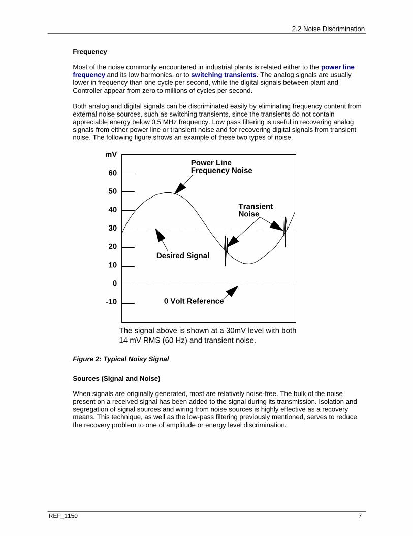
Most of the noise commonly encountered in industrial plants is related either to the power line frequency and its low harmonics, or to switching transients. The analog signals are usually lower in frequency than one cycle per second, while the digital signals between plant and Controller appear from zero to millions of cycles per second.
Both analog and digital signals can be discriminated easily by eliminating frequency content from external noise sources, such as switching transients, since the transients do not contain appreciable energy below 0.5 MHz frequency. Low pass filtering is useful in recovering analog signals from either power line or transient noise and for recovering digital signals from transient noise. The following figure shows an example of these two types of noise.
mV
60
50
40
30
20
10
0
-10
Power LineFrequency Noise
0 Volt Reference
Desired Signal
TransientNoise
The signal above is shown at a 30mV level with both14 mV RMS (60 Hz) and transient noise.
Figure 2: Typical Noisy Signal
Sources (Signal and Noise)
When signals are originally generated, most are relatively noise-free. The bulk of the noise present on a received signal has been added to the signal during its transmission. Isolation and segregation of signal sources and wiring from noise sources is highly effective as a recovery means. This technique, as well as the low-pass filtering previously mentioned, serves to reduce the recovery problem to one of amplitude or energy level discrimination.
2.3 Noise Sources
8 REF_1150
2.3 NOISE SOURCES
The following devices and circuits are common sources of noise:
Inductive devices, such as relays and solenoids. AC and DC power circuits, and wiring. Switchgear. Fast-rise-time sources: thyristors and certain solid-state switching circuits. Variable-frequency or variable current devices.
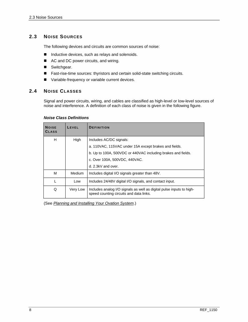
2.4 NOISE CLASSES
Signal and power circuits, wiring, and cables are classified as high-level or low-level sources of noise and interference. A definition of each class of noise is given in the following figure.
Noise Class Definitions
NOI SE CL AS S
LEV E L DE FI N I T I O N
H High Includes AC/DC signals:
a. 110VAC, 115VAC under 15A except brakes and fields.
b. Up to 100A, 500VDC or 440VAC including brakes and fields.
c. Over 100A, 500VDC, 440VAC.
d. 2.3kV and over.
M Medium Includes digital I/O signals greater than 48V.
L Low Includes 24/48V digital I/O signals, and contact input.
Q Very Low Includes analog I/O signals as well as digital pulse inputs to high-speed counting circuits and data links.
(See Planning and Installing Your Ovation System.)
2.5 Noise Rejection
REF_1150 9
2.5 NOISE REJECTION
2.5.1 WHAT TYPES OF DIGITAL SIGNAL NOISE REJECTION ARE USED?
The Ovation System employs three specific noise rejection measures for digital signal plant interconnections:
Low pass filtering. Substantial signal levels (48 VDC or 115 VAC). Isolation or optical coupling.
Low pass filtering and the use of large signal level techniques provide frequency and energy level discrimination, respectively.
Isolation of the digital signal receiver from ground is important as a means for rejecting noise which causes both wires in a signal pair to change voltage-to-ground potentials. An example of this type of isolation is a signal source (transmitter) which is grounded at a point remote from the receiver, where transmitter and receiver grounds are not at the same voltage. In this case, ground potential difference appears as a voltage on both wires of the corresponding signal pair.
Another example in which isolation may be required to reject ground potential difference noise would be in circuits where coupling exists between signal wires, inducing a potential in both wires. Induced potentials can occur when signal wires are present in environments with changing electromagnetic or electrostatic fields. Isolation may be required in this case.
An optical isolator (also known as an opto-isolator) may be used to bring digital signals into the receiver. No receiver response to noise can occur unless signal line noise current flows. Low frequency current, which may flow as a result of equal noise voltage-to-ground potentials on both wires of the signal pair, is eliminated if the signal wires are not grounded at more than one point. This is called the common-mode voltage.
Note: High frequency noise currents can flow using stray capacitance as part of their path. This requires the use of low pass filtering in addition to the optical isolation.
Analog Signal Noise Rejection
Analog signal isolation is provided for the same reasons that are discussed for digital signals (see page 9). However, since analog signals are typically low level, filtering and isolation noise rejection techniques are more critical for analog signals than for digital signals.
Analog signal filtering is achieved by averaging applied signals for one cycle (or an integer multiple of cycles) of the AC power line frequency. Power line related noise, at the power line frequency and its harmonics, has exactly zero average value when the average is taken over exactly one cycle and is filtered out of the signal by this technique.
Transient noise (high frequency damped ringing) has zero average value for averages taken over time periods much longer than the duration of the transients.
2.5 Noise Rejection
10 REF_1150
Output Signal Noise Rejection
Digital output signals from the Ovation System to the plant are electromechanical or semiconductor outputs which are electrically isolated from the Controller. Analog output signals from the Ovation system to the plant are either voltage or current outputs which are also electrically isolated from the Controller.
Noise-Sensitive Circuit Noise Rejection
All transmitting, low-level analog and digital circuits must be assumed to be noise-sensitive and to require special protection against noise. Field signals from process transducers (thermocouples, RTDs, and so forth) are especially susceptible to noise. Noise can be coupled into these sensitive circuits in three ways:
Electrostatic coupling via distributed capacitances. Electromagnetic coupling via distributed inductances. Conductive coupling, such as circuits sharing a common return.
Noise suppression for these noise sensitive circuits involves one or more of the following basic measures:
Physical separation (see page 10) between noise-producing and noise-sensitive circuits. Twisted-pair wiring (see page 10) for signal connection within plant. Proper grounding (see page 11), especially avoiding multiple grounding of cable shields and
proper shielding, especially cable shielding. Surge protection (see page 11) to IEEE and ANSI standards.
PHYSICAL CIRCUIT SEPARATION
Circuit separation is a simple and effective means of electrostatic and electromagnetic field induced noise control. This is because electrostatic and electromagnetic fields decay with increasing distance, producing lower amplitude noise and maintaining a good signal-to-noise ratio.
TWISTED-PAIR WIRING
Twisted-pair wiring suppresses noise by acting to eliminate circuit loops which are sensitive to stray electromagnetic fields. For this reason, it is recommended that all analog signal circuit connections should be made with twisted-pair wire. Digital signal connections should carry a group return (or common) wired in the same cable as the signal wires.
Twisted pairs are also recommended in digital circuits where unusually noisy environments exist. Twisting of the signal wire and its return conductor becomes increasingly important as the length of the two becomes greater, and as the distance from noise sources becomes less. In twisted pairs or small cables (less than 1/2 inch outer conductor circle diameter), a twist rate of at least one to two twists per foot is recommended.
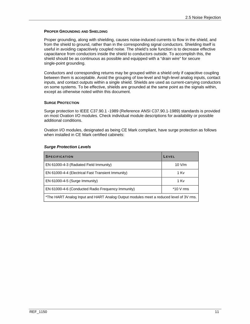
2.5 Noise Rejection
REF_1150 11
PROPER GROUNDING AND SHIELDING
Proper grounding, along with shielding, causes noise-induced currents to flow in the shield, and from the shield to ground, rather than in the corresponding signal conductors. Shielding itself is useful in avoiding capacitively coupled noise. The shield’s sole function is to decrease effective capacitance from conductors inside the shield to conductors outside. To accomplish this, the shield should be as continuous as possible and equipped with a “drain wire” for secure single-point grounding.
Conductors and corresponding returns may be grouped within a shield only if capacitive coupling between them is acceptable. Avoid the grouping of low-level and high-level analog inputs, contact inputs, and contact outputs within a single shield. Shields are used as current-carrying conductors on some systems. To be effective, shields are grounded at the same point as the signals within, except as otherwise noted within this document.
SURGE PROTECTION
Surge protection to IEEE C37.90.1 -1989 (Reference ANSI C37.90.1-1989) standards is provided on most Ovation I/O modules. Check individual module descriptions for availability or possible additional conditions.
Ovation I/O modules, designated as being CE Mark compliant, have surge protection as follows when installed in CE Mark certified cabinets:
Surge Protection Levels
SP E CI F I C AT I O N LEV E L
EN 61000-4-3 (Radiated Field Immunity) 10 V/m
EN 61000-4-4 (Electrical Fast Transient Immunity) 1 Kv
EN 61000-4-5 (Surge Immunity) 1 Kv
EN 61000-4-6 (Conducted Radio Frequency Immunity) *10 V rms
*The HART Analog Input and HART Analog Output modules meet a reduced level of 3V rms.
2.6 Analog Signal Shielding Techniques
12 REF_1150
2.6 ANALOG SIGNAL SHIELDING TECHNIQUES
For noise suppression purposes, analog signals of less than one volt is considered low-level and (as is the case with all analog signals), require shielding. Individually twisted and shielded pairs should be used for all analog input signal wiring. Multi-pair cable can be used if each twisted pair in the cable has its own insulated shield. Use the following guidelines to shield signals:
Ground the analog signal shield. Ground the shield at one end only, preferably to a single point at the signal source, except as
otherwise noted in this document. Connect the low side of the signal to the shield at the signal source. If the shield cannot be
conveniently grounded at or near the signal source, ground it at the Controller. An ideal analog signal field connection is shown in the following figure
Run the shield (unbroken) from the transducer to the shield terminal of the Analog to Digital (A/D) front-end at the Analog Input module. (See Planning and Installing Your Ovation System.) Maintain shield continuity at junction boxes when they are used.
A/D
A/D Guard
Twisted Pair
UnbrokenCable Shield
Drain Wire
Single PointGround
ES
Figure 3: Ideal Analog Signal Field Connection
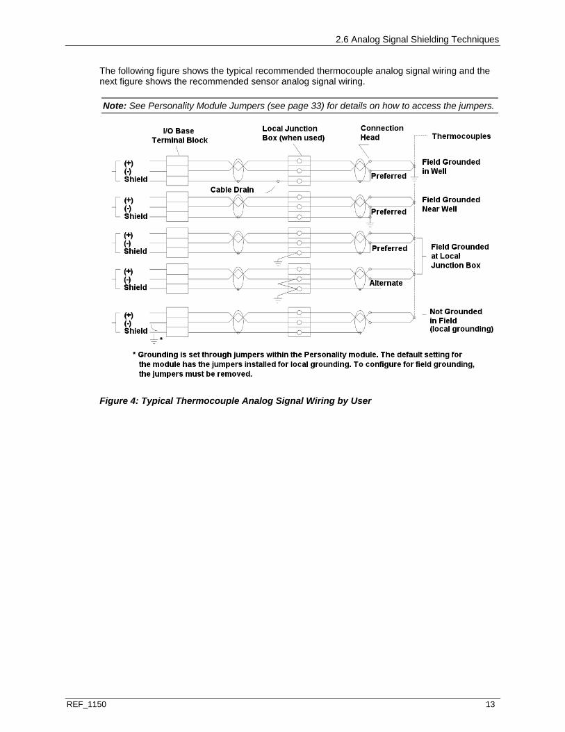
2.6 Analog Signal Shielding Techniques
REF_1150 13
The following figure shows the typical recommended thermocouple analog signal wiring and the next figure shows the recommended sensor analog signal wiring.
Note: See Personality Module Jumpers (see page 33) for details on how to access the jumpers.
Figure 4: Typical Thermocouple Analog Signal Wiring by User
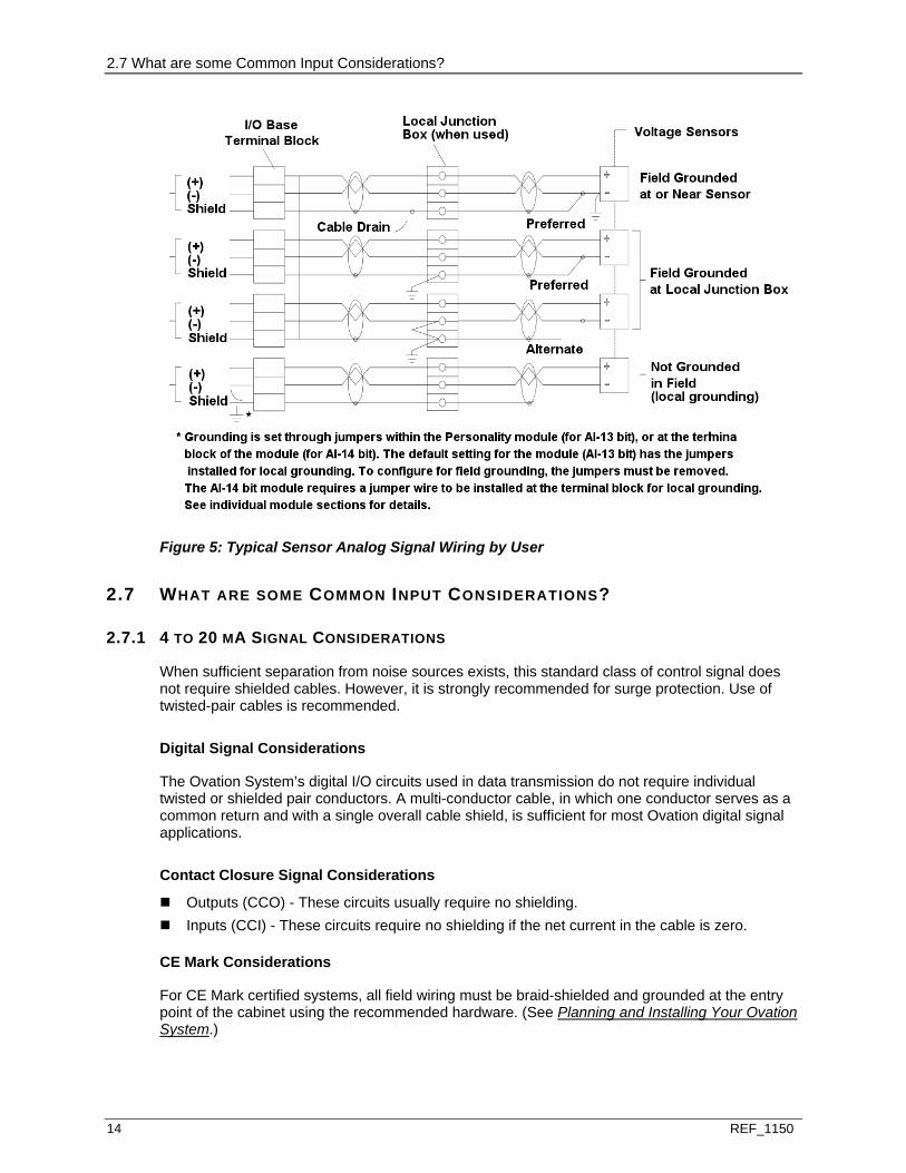
2.7 What are some Common Input Considerations?
14 REF_1150
Figure 5: Typical Sensor Analog Signal Wiring by User
2.7 WHAT ARE SOME COMMON INPUT CONSIDERATIONS?
2.7.1 4 TO 20 MA SIGNAL CONSIDERATIONS
When sufficient separation from noise sources exists, this standard class of control signal does not require shielded cables. However, it is strongly recommended for surge protection. Use of twisted-pair cables is recommended.
Digital Signal Considerations
The Ovation System’s digital I/O circuits used in data transmission do not require individual twisted or shielded pair conductors. A multi-conductor cable, in which one conductor serves as a common return and with a single overall cable shield, is sufficient for most Ovation digital signal applications.
Contact Closure Signal Considerations
Outputs (CCO) - These circuits usually require no shielding. Inputs (CCI) - These circuits require no shielding if the net current in the cable is zero.
CE Mark Considerations
For CE Mark certified systems, all field wiring must be braid-shielded and grounded at the entry point of the cabinet using the recommended hardware. (See Planning and Installing Your Ovation System.)
REF_1150 15
IN THIS SECTION
What General Information Should I Know About Ovation I/O Modules? .......................... 15 What are the I/O Module Types? ......................................................................................22 Ovation Module Choices ...................................................................................................25 Installing Ovation Modules ................................................................................................29 Ovation Module Configuration and Status ........................................................................30 Ovation Module Diagnostic LEDs .....................................................................................30 What is Involved in the Replacement of User Serviceable Fuses? .................................. 31 Personality Module Jumpers.............................................................................................33 I/O Environmental Specifications ......................................................................................34
3.1 WHAT GENERAL INFORMATION SHOULD I KNOW ABOUT OVATION I/O MODULES?
The following information gives an over-all view of the standard Ovation Electronic and Personality Modules including:
Features (see page 16) I/O Module types (see page 22) Module choices (see page 25) (which personality modules go with which electronic modules) Installation (see page 29) Configuration (see page 30) Diagnostics LEDs (see page 30) User Serviceable Fuses (see page 31) Personality Module Jumpers (see page 33) I/O environmental specifications (see page 34)
S E C T I O N 3
I/O MODULE GENERAL INFORMATION
3.1 What General Information Should I Know About Ovation I/O Modules?
16 REF_1150
3.1.1 OVATION MODULE FEATURES Ovation I/O is available in both remote and local configurations. Modular, “plug-in” components. Quick installation and configuration of the modules. DIN Rail mounting of the I/O Base Units. Wiring schematic labels are provided on Personality modules and foam inserts. Wiring directions (Normally Closed, Normally Open, Common) are provided on the Base Unit
for Relay Output modules. Writable surface labels are provided on Electronics modules so that up to 16 point names can
be identified on each label. The labels on the Personality and Electronics modules are color-coded to match the
appropriate modules. Unique base unit interconnection scheme eliminates most power and communications wiring. Module style, group, serial number, and revision are stored electronically on each I/O module. “Hot swapping” capabilities streamline maintenance. (See Planning and Installing Your
Ovation System.) Status indicators that display standardized diagnostic LED color codes. Up to 128 Local Ovation module units per Controller. Up to 1024 Remote Ovation module units per Controller. Base Unit common to all Standard I/O modules. Two Base Unit styles (G2R and KUEP) are available for Relay Output modules. Testpoint/probe holder on each field terminal of standard I/O Base Units. Built-in spare fuse holders and wire strip gauge in standard I/O Base Units. Most modules are CE Mark compliant.
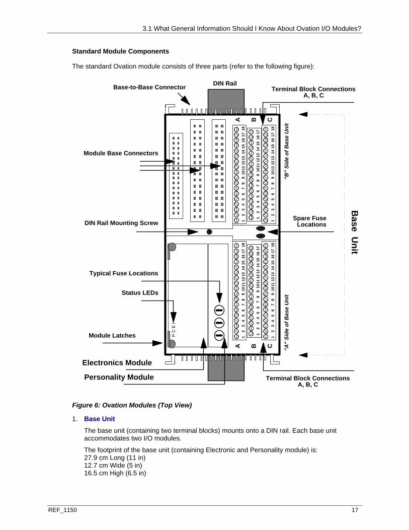
3.1 What General Information Should I Know About Ovation I/O Modules?
REF_1150 17
Standard Module Components
The standard Ovation module consists of three parts (refer to the following figure):
12
34
56
78
910
1112
1314
1516
1718
12
34
56
78
910
1112
1314
1516
1718
12
34
56
78
910
1112
1314
1516
17
A B C
12
34
56
78
910
1112
1314
1516
1718
12
34
56
78
910
1112
1314
1516
1718
12
34
56
78
910
1112
1314
1516
17
A B C
P C
E I
DIN Rail
Module Base Connectors
DIN Rail Mounting Screw
Terminal Block ConnectionsA, B, C
Status LEDs
Typical Fuse Locations
Electronics Module
Base-to-Base Connector Terminal Block ConnectionsA, B, C
Base U
nit
Personality Module
Spare Fuse Locations
"A"
Side
of B
ase
Uni
t"B
" Si
de o
f Bas
e U
nit
Module Latches
Figure 6: Ovation Modules (Top View)
1. Base Unit
The base unit (containing two terminal blocks) mounts onto a DIN rail. Each base unit accommodates two I/O modules.
The footprint of the base unit (containing Electronic and Personality module) is: 27.9 cm Long (11 in) 12.7 cm Wide (5 in) 16.5 cm High (6.5 in)
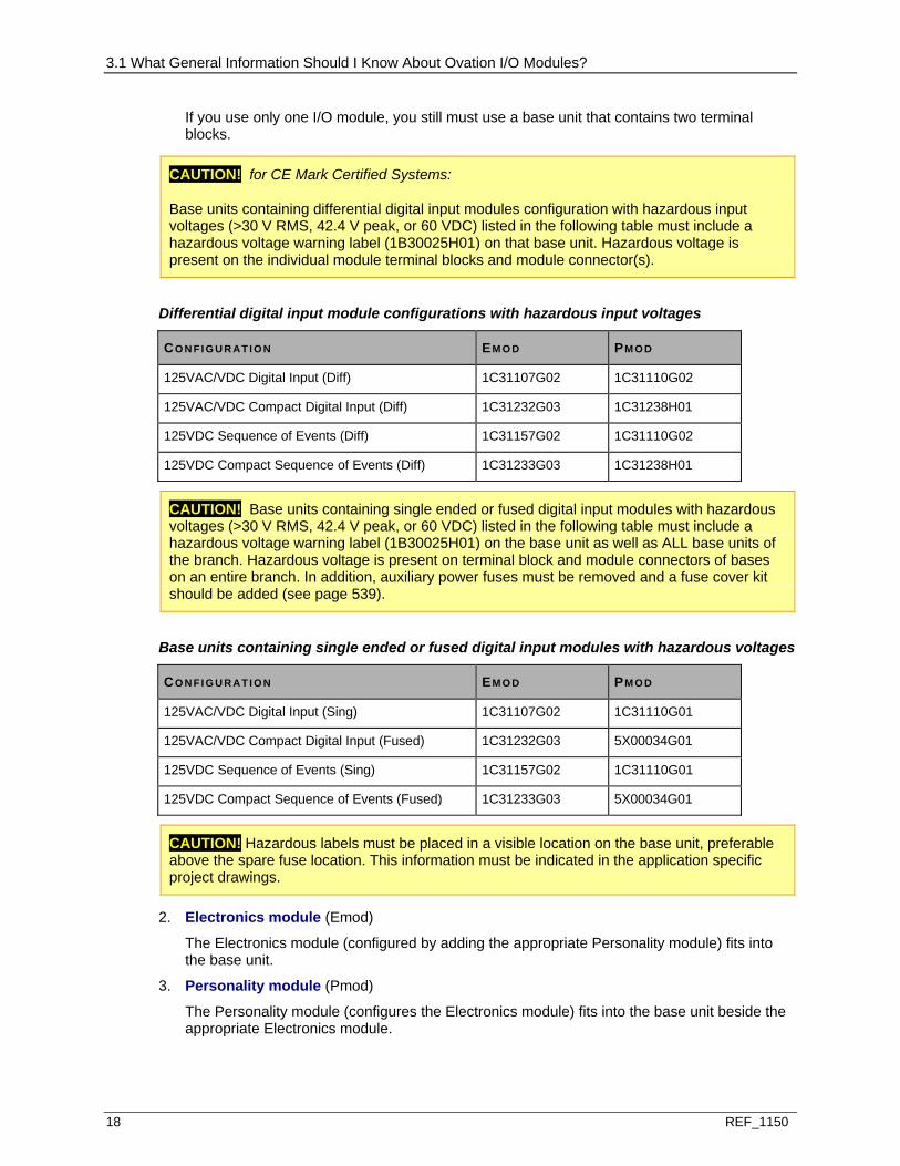
3.1 What General Information Should I Know About Ovation I/O Modules?
18 REF_1150
If you use only one I/O module, you still must use a base unit that contains two terminal blocks.
CAUTION! for CE Mark Certified Systems:
Base units containing differential digital input modules configuration with hazardous input voltages (>30 V RMS, 42.4 V peak, or 60 VDC) listed in the following table must include a hazardous voltage warning label (1B30025H01) on that base unit. Hazardous voltage is present on the individual module terminal blocks and module connector(s).
Differential digital input module configurations with hazardous input voltages
CO N FI G U R AT I O N EM O D PM O D
125VAC/VDC Digital Input (Diff) 1C31107G02 1C31110G02
125VAC/VDC Compact Digital Input (Diff) 1C31232G03 1C31238H01
125VDC Sequence of Events (Diff) 1C31157G02 1C31110G02
125VDC Compact Sequence of Events (Diff) 1C31233G03 1C31238H01
CAUTION! Base units containing single ended or fused digital input modules with hazardous voltages (>30 V RMS, 42.4 V peak, or 60 VDC) listed in the following table must include a hazardous voltage warning label (1B30025H01) on the base unit as well as ALL base units of the branch. Hazardous voltage is present on terminal block and module connectors of bases on an entire branch. In addition, auxiliary power fuses must be removed and a fuse cover kit should be added (see page 539).
Base units containing single ended or fused digital input modules with hazardous voltages
CO N FI G U R AT I O N EM O D PM O D
125VAC/VDC Digital Input (Sing) 1C31107G02 1C31110G01
125VAC/VDC Compact Digital Input (Fused) 1C31232G03 5X00034G01
125VDC Sequence of Events (Sing) 1C31157G02 1C31110G01
125VDC Compact Sequence of Events (Fused) 1C31233G03 5X00034G01
CAUTION! Hazardous labels must be placed in a visible location on the base unit, preferable above the spare fuse location. This information must be indicated in the application specific project drawings.
2. Electronics module (Emod)
The Electronics module (configured by adding the appropriate Personality module) fits into the base unit.
3. Personality module (Pmod)
The Personality module (configures the Electronics module) fits into the base unit beside the appropriate Electronics module.
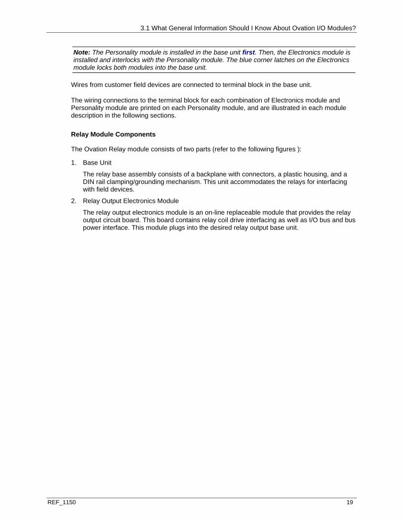
3.1 What General Information Should I Know About Ovation I/O Modules?
REF_1150 19
Note: The Personality module is installed in the base unit first. Then, the Electronics module is installed and interlocks with the Personality module. The blue corner latches on the Electronics module locks both modules into the base unit.
Wires from customer field devices are connected to terminal block in the base unit.
The wiring connections to the terminal block for each combination of Electronics module and Personality module are printed on each Personality module, and are illustrated in each module description in the following sections.
Relay Module Components
The Ovation Relay module consists of two parts (refer to the following figures ):
1. Base Unit
The relay base assembly consists of a backplane with connectors, a plastic housing, and a DIN rail clamping/grounding mechanism. This unit accommodates the relays for interfacing with field devices.
2. Relay Output Electronics Module
The relay output electronics module is an on-line replaceable module that provides the relay output circuit board. This board contains relay coil drive interfacing as well as I/O bus and bus power interface. This module plugs into the desired relay output base unit.
3.1 What General Information Should I Know About Ovation I/O Modules?
20 REF_1150
The wires from the customer field devices are connected to the terminal block in the base unit.
DIN Rail
DIN Rail Mounting Screw
Base-to-Base Connector
Base U
nit
Module Latches
R7
R6
R5
R4
R3
R2
R1
R8
R15
R14
R13
R12
R11
R10
R9
R16
TB1
Electronics Module
Fuse
Terminal BlockConnections
"A"
Side
of B
ase
Uni
t"B
" Si
de o
f Bas
e U
nit
LOC
KED
OPE
NP
CE
I2
34
56
78
910
1112
1314
1516
REL
AY
OU
TPU
T
1C31
219G
01LO
CK
ED
OPE
N1
TB2
TB3
TB4
TB5
TB6
TB7
TB8
TB9
TB10
TB11
TB12
TB13
TB14
TB15
TB16
Figure 7: Relay Output Panel G2R
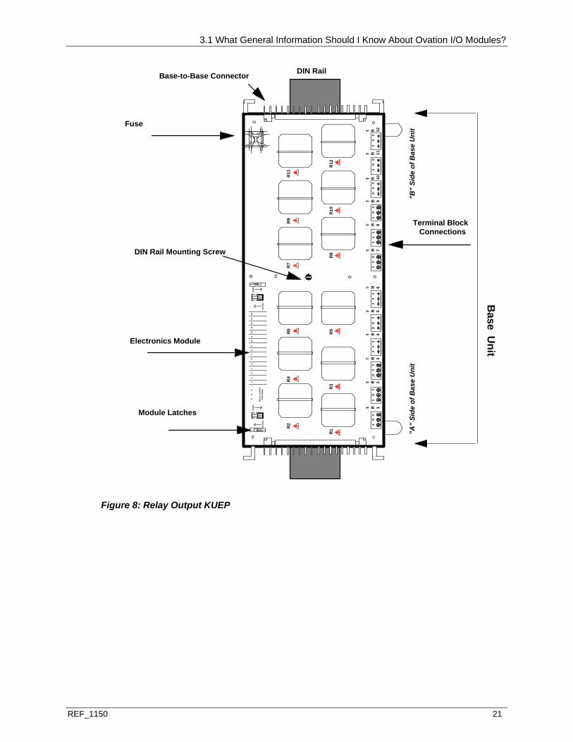
3.1 What General Information Should I Know About Ovation I/O Modules?
REF_1150 21
DIN Rail
DIN Rail Mounting Screw
Base-to-Base ConnectorB
ase Unit
Module Latches
Electronics Module
Fuse
Terminal BlockConnections
"A"
Side
of B
ase
Uni
t"B
" Si
de o
f Bas
e U
nit
LOC
KED
OPE
NP
CE
I2
34
56
78
910
1112
1314
1516
REL
AY
OU
TPU
T
1C31
219G
01LO
CK
ED
OPE
N
R1R
2
R3
R4
R6
R5
R8
R7
R9
R10
R12
R11
T B 1
T B 2
T B 3
T B 4
T B 5
T B 6
T B 7
T B 8
T B 9
T B 10
T B 11
T B 12
1
Figure 8: Relay Output KUEP
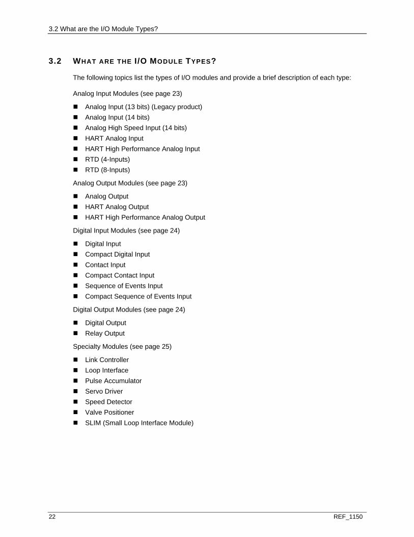
3.2 What are the I/O Module Types?
22 REF_1150
3.2 WHAT ARE THE I/O MODULE TYPES?
The following topics list the types of I/O modules and provide a brief description of each type:
Analog Input Modules (see page 23)
Analog Input (13 bits) (Legacy product) Analog Input (14 bits) Analog High Speed Input (14 bits) HART Analog Input HART High Performance Analog Input RTD (4-Inputs) RTD (8-Inputs)
Analog Output Modules (see page 23)
Analog Output HART Analog Output HART High Performance Analog Output
Digital Input Modules (see page 24)
Digital Input Compact Digital Input Contact Input Compact Contact Input Sequence of Events Input Compact Sequence of Events Input
Digital Output Modules (see page 24)
Digital Output Relay Output
Specialty Modules (see page 25)
Link Controller Loop Interface Pulse Accumulator Servo Driver Speed Detector Valve Positioner SLIM (Small Loop Interface Module)
3.2 What are the I/O Module Types?
REF_1150 23
3.2.1 ANALOG INPUT MODULES
Analog Input (13 bits) (see page 37) - (Legacy product) - provides interface to eight individually isolated analog inputs with sampling rates of approximately 10 time/sec. Several voltage and current configurations are available including cold junction compensation for thermocouple inputs.
Analog Input (14 bits) (see page 55) - provides an interface to eight individually isolated analog inputs with a minimum sampling rate of 10 time/sec. A low cost 4-20 mA current input is available along with a 1V voltage input (legacy) configuration.
Analog High Speed Input (14 bits) (see page 67) - provides an interface to eight individually isolated analog inputs with sampling rates of medium speed (16/20 time/sec.) or high speed (50/60 times/sec.). Several voltage and current input configurations are available including cold junction compensation for thermocouple inputs.
HART Analog Input (see page 177) - provides an interface for eight HART field devices with 4-20 mA current loop analog inputs (common reference). In addition to the analog inputs, digital information can be exchanged between HART compliant devices and the Controller.
HART High Performance Analog Input (see page 193) - provides an interface for eight HART field devices with 4-20 mA current loop analog inputs (common reference). In addition to the analog inputs, digital information can be exchanged between HART compliant devices and the Controller.
RTD 4-Input (see page 305) - provides an interface to four Resistance Temperature Detectors. Several 3 and 4 wire RTD types are supported. A 50/60 Hz filtered configuration is available for CE Mark applications.
RTD 8-Input (see page 317) - provides interface to eight Resistance Temperature Detectors. Several 3 and 4 wire RTD types are supported.
3.2.2 ANALOG OUTPUT MODULES
Analog Output (see page 93) - provides an interface to four individually isolated analog outputs using 12 bit digital-to-analog converters.
HART Analog Output (see page 207) - provides an interface for eight HART field devices with 4-20 mA current loop analog outputs (common reference). In addition to the outputs, digital information can be exchanged between HART compliant devices and the Controller.
HART High Performance Analog Output (see page 223) - provides an interface for eight HART field devices with 4-20 mA current loop analog outputs (common reference). In addition to the outputs, digital information can be exchanged between HART compliant devices and the Controller.
3.2 What are the I/O Module Types?
24 REF_1150
3.2.3 DIGITAL INPUT MODULES
Digital Input (see page 125) - provides an interface for 16 digital inputs. The following input configurations are available: 24V, 48V, and 125V Isolated Differential or Single Ended (common return).
Compact Digital Input (see page 137) - provides a low cost interface for 16 digital inputs by eliminating the need for a Pmod. The following input configurations are available: 24V or 48V Isolated Differential or Single Ended (common return), or 125V isolated differential. If desired, a Pmod can be added to individually fuse inputs (with common return).
Contact Input (see page 101) - provides an interface for 16 digital contact inputs with common return. A +48V on-board power supply provides current limited contact wetting.
Compact Contact Input (see page 113) - provides a low cost interface for 16 digital contact inputs with common return by eliminating the need for a Pmod. A +48V on-board power supply provides current limited contact wetting.
Sequence of Events Input (see page 329) - provides an interface for 16 digital inputs with time tagging information to within 125 ms. An event tagging mask and filters to reject state changes and input chatter are provided along with time synchronization to the Controller with 1 ms resolution. Several input configurations are available.
Compact Sequence of Events Input (see page 351) - provides a low cost interface for 16 digital inputs with time tagging information to within 125 ms. An event tagging mask and filters to reject state changes and input chatter is provided along with time synchronization to the Controller with 1 ms resolution. Several input configurations are available. If desired, a Pmod can be added to individually fuse the inputs (with common return).
3.2.4 DIGITAL OUTPUT MODULES
Digital Output (see page 151) - provides an interface to 16 single ended digital outputs. 5 to 60 VDC loads up to 500 mA each can be controlled (Total current limited by fuse rating.) This module can also be used to interface KU, G2R or solid state relay panels for increased switching capability.
Relay Output (see page 291) - provides an interface to either 12 KU relay or 16 G2R relay outputs. Special relay bases connect directly to the Ovation I/O branches and house the Relay Output Electronics module and relays.
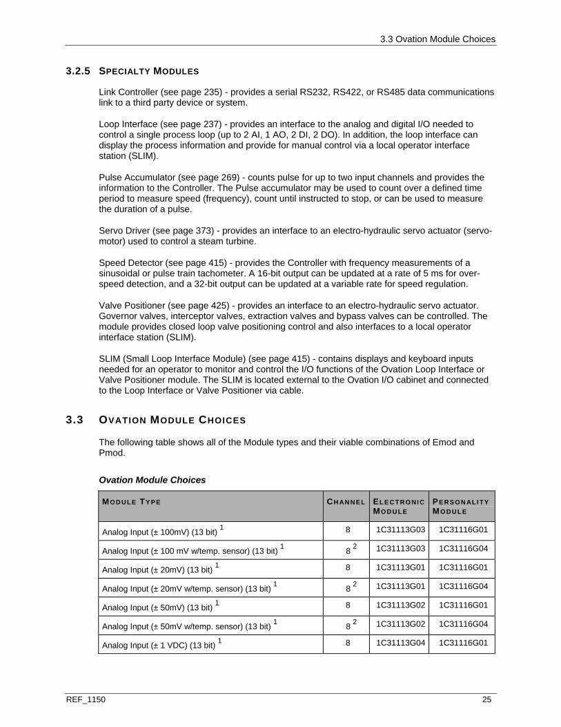
3.3 Ovation Module Choices
REF_1150 25
3.2.5 SPECIALTY MODULES
Link Controller (see page 235) - provides a serial RS232, RS422, or RS485 data communications link to a third party device or system.
Loop Interface (see page 237) - provides an interface to the analog and digital I/O needed to control a single process loop (up to 2 AI, 1 AO, 2 DI, 2 DO). In addition, the loop interface can display the process information and provide for manual control via a local operator interface station (SLIM).
Pulse Accumulator (see page 269) - counts pulse for up to two input channels and provides the information to the Controller. The Pulse accumulator may be used to count over a defined time period to measure speed (frequency), count until instructed to stop, or can be used to measure the duration of a pulse.
Servo Driver (see page 373) - provides an interface to an electro-hydraulic servo actuator (servo-motor) used to control a steam turbine.
Speed Detector (see page 415) - provides the Controller with frequency measurements of a sinusoidal or pulse train tachometer. A 16-bit output can be updated at a rate of 5 ms for over-speed detection, and a 32-bit output can be updated at a variable rate for speed regulation.
Valve Positioner (see page 425) - provides an interface to an electro-hydraulic servo actuator. Governor valves, interceptor valves, extraction valves and bypass valves can be controlled. The module provides closed loop valve positioning control and also interfaces to a local operator interface station (SLIM).
SLIM (Small Loop Interface Module) (see page 415) - contains displays and keyboard inputs needed for an operator to monitor and control the I/O functions of the Ovation Loop Interface or Valve Positioner module. The SLIM is located external to the Ovation I/O cabinet and connected to the Loop Interface or Valve Positioner via cable.
3.3 OVATION MODULE CHOICES
The following table shows all of the Module types and their viable combinations of Emod and Pmod.
Ovation Module Choices
MO D U LE TY PE CH AN N E L EL E C T RO NI C MO D U LE
PE R S O N AL I T Y MO D U LE
Analog Input (± 100mV) (13 bit) 1 8 1C31113G03 1C31116G01
Analog Input (± 100 mV w/temp. sensor) (13 bit) 1 8 2 1C31113G03 1C31116G04
Analog Input (± 20mV) (13 bit) 1 8 1C31113G01 1C31116G01
Analog Input (± 20mV w/temp. sensor) (13 bit) 1 8 2 1C31113G01 1C31116G04
Analog Input (± 50mV) (13 bit) 1 8 1C31113G02 1C31116G01
Analog Input (± 50mV w/temp. sensor) (13 bit) 1 8 2 1C31113G02 1C31116G04
Analog Input (± 1 VDC) (13 bit) 1 8 1C31113G04 1C31116G01

3.3 Ovation Module Choices
26 REF_1150
MO D U LE TY PE CH AN N E L EL E C T RO NI C MO D U LE
PE R S O N AL I T Y MO D U LE
Analog Input (± 10 VDC) (13 bit) 1 8 1C31113G06 1C31116G01
Analog Input (± 5 VDC) (13 bit) 1 8 1C31113G05 1C31116G01
Analog Input (0-20 or 4-20 mA Local PS) (13 bit) 1 8 1C31113G05 1C31116G03
Analog Input (0-20 or 4-20 mA Remote PS) (13 bit) 1 8 1C31113G05 1C31116G02
Analog Input (4-20 mA) (14 bit Low Speed) 8 1C31224G01 1C31227G01
Analog Input (± 1 VDC) (14 bit Low Speed) 1 8 1C31224G02 1C31227G02
Analog Input (4-20 mA) (14 bit High Speed (HS)) 8 5X00070G01 1C31227G01
Analog Input (± 100mV, ± 250mV, ± 1V) (14 bit HS) 8 5X00070G02 1C31227G02
Analog Input (± 5V, ± 10V) (14 bit HS) 8 5X00070G03 1C31227G02
Analog Input (± 1mA, (using 250mV) 2 wire Local PS) (14 bit HS) (Turbine)
8 5X00070G02 1C31116G03
Analog Input (± 1mA, (using 250mV) 4wire field powered) (14 bit HS) (Turbine)
8 5X00070G02 1C31116G02
Analog Input (± 20mV, ± 50mV, ± 100mV) (Thermocouple) (14 bit MS)
8 5X00070G04 1C31116G04
Analog Output (0 to +10 V) 4 1C31129G02 1C31132G01
Analog Output (0 to +5 V) 4 1C31129G01 1C31132G01
Analog Output (0-20 or 4-20 mA w/diagnostics) 4 1C31129G03 1C31132G01
Analog Output (0-20 or 4-20 mA w/o diagnostics) 4 1C31129G04 1C31132G01
Contact Input w/Onboard 48 V wetting (Compact) 16 1C31234G01 Cavity Insert 3
Contact Input w/Onboard 48 V wetting 1 16 1C31142G01 1C31110G03
Digital Input (125 VAC/VDC differential) 1 16 1C31107G02 1C31110G02
Digital Input (125 VAC/VDC single ended) 16 1C31107G02 1C31110G01
Digital Input (24 VAC/VDC or 48 VDC differential) 1 16 1C31107G01 1C31110G02
Digital Input (24 VAC/VDC or 48 VDC single ended) 1 16 1C31107G01 1C31110G01
Digital Input (125 VAC/VDC Indiv. Fused) (Compact) 16 1C31232G03 5X00034G01
Digital Input (125 VAC/VDC differential) (Compact) 16 1C31232G03 Cavity Insert 3
Digital Input (24/48 VAC/VDC Indiv. Fused) (Compact) 16 1C31232G02 5X00034G01
Digital Input (24 or 48 VAC/VDC differential) (Compact) 16 1C31232G02 Cavity Insert 3
Digital Input (24 or 48 VDC single ended) (Compact) 16 1C31232G01 Cavity Insert 3
Digital Output (5-60 VDC) Single ended direct 16 1C31122G01 1C31125G01
Digital Output (relay pnl comm, Local PS) 16 1C31122G01 1C31125G02
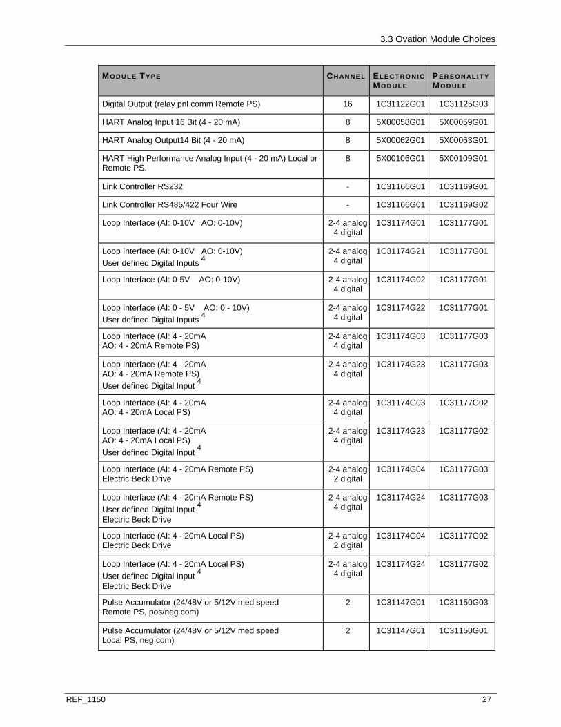
3.3 Ovation Module Choices
REF_1150 27
MO D U LE TY PE CH AN N E L EL E C T RO NI C MO D U LE
PE R S O N AL I T Y MO D U LE
Digital Output (relay pnl comm Remote PS) 16 1C31122G01 1C31125G03
HART Analog Input 16 Bit (4 - 20 mA) 8 5X00058G01 5X00059G01
HART Analog Output14 Bit (4 - 20 mA) 8 5X00062G01 5X00063G01
HART High Performance Analog Input (4 - 20 mA) Local or Remote PS.
8 5X00106G01 5X00109G01
Link Controller RS232 - 1C31166G01 1C31169G01
Link Controller RS485/422 Four Wire - 1C31166G01 1C31169G02
Loop Interface (AI: 0-10V AO: 0-10V) 2-4 analog4 digital
1C31174G01 1C31177G01
Loop Interface (AI: 0-10V AO: 0-10V) User defined Digital Inputs 4
2-4 analog4 digital
1C31174G21 1C31177G01
Loop Interface (AI: 0-5V AO: 0-10V) 2-4 analog4 digital
1C31174G02 1C31177G01
Loop Interface (AI: 0 - 5V AO: 0 - 10V) User defined Digital Inputs 4
2-4 analog4 digital
1C31174G22 1C31177G01
Loop Interface (AI: 4 - 20mA AO: 4 - 20mA Remote PS)
2-4 analog4 digital
1C31174G03 1C31177G03
Loop Interface (AI: 4 - 20mA AO: 4 - 20mA Remote PS) User defined Digital Input 4
2-4 analog4 digital
1C31174G23 1C31177G03
Loop Interface (AI: 4 - 20mA AO: 4 - 20mA Local PS)
2-4 analog4 digital
1C31174G03 1C31177G02
Loop Interface (AI: 4 - 20mA AO: 4 - 20mA Local PS) User defined Digital Input 4
2-4 analog4 digital
1C31174G23 1C31177G02
Loop Interface (AI: 4 - 20mA Remote PS) Electric Beck Drive
2-4 analog2 digital
1C31174G04 1C31177G03
Loop Interface (AI: 4 - 20mA Remote PS) User defined Digital Input 4 Electric Beck Drive
2-4 analog4 digital
1C31174G24 1C31177G03
Loop Interface (AI: 4 - 20mA Local PS) Electric Beck Drive
2-4 analog2 digital
1C31174G04 1C31177G02
Loop Interface (AI: 4 - 20mA Local PS) User defined Digital Input 4 Electric Beck Drive
2-4 analog4 digital
1C31174G24 1C31177G02
Pulse Accumulator (24/48V or 5/12V med speed Remote PS, pos/neg com)
2 1C31147G01 1C31150G03
Pulse Accumulator (24/48V or 5/12V med speed Local PS, neg com)
2 1C31147G01 1C31150G01
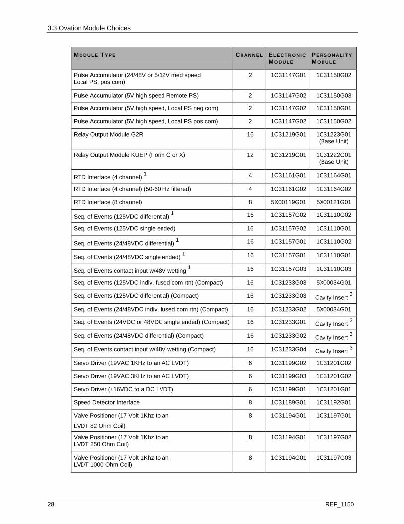
3.3 Ovation Module Choices
28 REF_1150
MO D U LE TY PE CH AN N E L EL E C T RO NI C MO D U LE
PE R S O N AL I T Y MO D U LE
Pulse Accumulator (24/48V or 5/12V med speed Local PS, pos com)
2 1C31147G01 1C31150G02
Pulse Accumulator (5V high speed Remote PS) 2 1C31147G02 1C31150G03
Pulse Accumulator (5V high speed, Local PS neg com) 2 1C31147G02 1C31150G01
Pulse Accumulator (5V high speed, Local PS pos com) 2 1C31147G02 1C31150G02
Relay Output Module G2R 16 1C31219G01 1C31223G01 (Base Unit)
Relay Output Module KUEP (Form C or X) 12 1C31219G01 1C31222G01 (Base Unit)
RTD Interface (4 channel) 1 4 1C31161G01 1C31164G01
RTD Interface (4 channel) (50-60 Hz filtered) 4 1C31161G02 1C31164G02
RTD Interface (8 channel) 8 5X00119G01 5X00121G01
Seq. of Events (125VDC differential) 1 16 1C31157G02 1C31110G02
Seq. of Events (125VDC single ended) 16 1C31157G02 1C31110G01
Seq. of Events (24/48VDC differential) 1 16 1C31157G01 1C31110G02
Seq. of Events (24/48VDC single ended) 1 16 1C31157G01 1C31110G01
Seq. of Events contact input w/48V wetting 1 16 1C31157G03 1C31110G03
Seq. of Events (125VDC indiv. fused com rtn) (Compact) 16 1C31233G03 5X00034G01
Seq. of Events (125VDC differential) (Compact) 16 1C31233G03 Cavity Insert 3
Seq. of Events (24/48VDC indiv. fused com rtn) (Compact) 16 1C31233G02 5X00034G01
Seq. of Events (24VDC or 48VDC single ended) (Compact) 16 1C31233G01 Cavity Insert 3
Seq. of Events (24/48VDC differential) (Compact) 16 1C31233G02 Cavity Insert 3
Seq. of Events contact input w/48V wetting (Compact) 16 1C31233G04 Cavity Insert 3
Servo Driver (19VAC 1KHz to an AC LVDT) 6 1C31199G02 1C31201G02
Servo Driver (19VAC 3KHz to an AC LVDT) 6 1C31199G03 1C31201G02
Servo Driver (±16VDC to a DC LVDT) 6 1C31199G01 1C31201G01
Speed Detector Interface 8 1C31189G01 1C31192G01
Valve Positioner (17 Volt 1Khz to an
LVDT 82 Ohm Coil)
8 1C31194G01 1C31197G01
Valve Positioner (17 Volt 1Khz to an LVDT 250 Ohm Coil)
8 1C31194G01 1C31197G02
Valve Positioner (17 Volt 1Khz to an LVDT 1000 Ohm Coil)
8 1C31194G01 1C31197G03
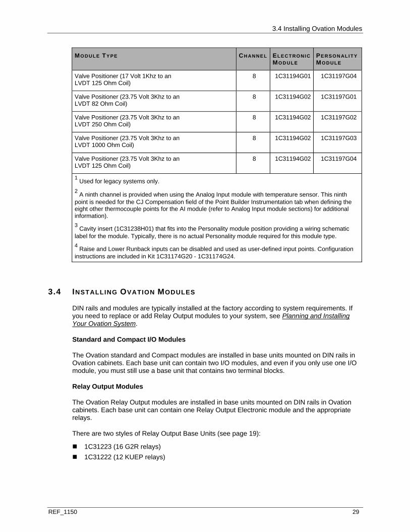
3.4 Installing Ovation Modules
REF_1150 29
MO D U LE TY PE CH AN N E L EL E C T RO NI C MO D U LE
PE R S O N AL I T Y MO D U LE
Valve Positioner (17 Volt 1Khz to an LVDT 125 Ohm Coil)
8 1C31194G01 1C31197G04
Valve Positioner (23.75 Volt 3Khz to an LVDT 82 Ohm Coil)
8 1C31194G02 1C31197G01
Valve Positioner (23.75 Volt 3Khz to an LVDT 250 Ohm Coil)
8 1C31194G02 1C31197G02
Valve Positioner (23.75 Volt 3Khz to an LVDT 1000 Ohm Coil)
8 1C31194G02 1C31197G03
Valve Positioner (23.75 Volt 3Khz to an LVDT 125 Ohm Coil)
8 1C31194G02 1C31197G04
1 Used for legacy systems only. 2 A ninth channel is provided when using the Analog Input module with temperature sensor. This ninth point is needed for the CJ Compensation field of the Point Builder Instrumentation tab when defining the eight other thermocouple points for the AI module (refer to Analog Input module sections) for additional information). 3 Cavity insert (1C31238H01) that fits into the Personality module position providing a wiring schematic label for the module. Typically, there is no actual Personality module required for this module type. 4 Raise and Lower Runback inputs can be disabled and used as user-defined input points. Configuration instructions are included in Kit 1C31174G20 - 1C31174G24.
3.4 INSTALLING OVATION MODULES
DIN rails and modules are typically installed at the factory according to system requirements. If you need to replace or add Relay Output modules to your system, see Planning and Installing Your Ovation System.
Standard and Compact I/O Modules
The Ovation standard and Compact modules are installed in base units mounted on DIN rails in Ovation cabinets. Each base unit can contain two I/O modules, and even if you only use one I/O module, you must still use a base unit that contains two terminal blocks.
Relay Output Modules
The Ovation Relay Output modules are installed in base units mounted on DIN rails in Ovation cabinets. Each base unit can contain one Relay Output Electronic module and the appropriate relays.
There are two styles of Relay Output Base Units (see page 19):
1C31223 (16 G2R relays) 1C31222 (12 KUEP relays)

3.5 Ovation Module Configuration and Status
30 REF_1150
3.5 OVATION MODULE CONFIGURATION AND STATUS
An Ovation I/O module has 16 address locations, but a module might not use all 16 addresses.
There are four possible address locations in each I/O module that are reserved for special use. Three of these addresses provide configuration (Write) and status (Read) information.
Definitions for these locations are provided for each module in the module reference pages:
Address word 13 (D in Hex) is present for every module and is used for configuration and status. The module status provides diagnostic information that is read by the Controller when it is on-line. The status register can be read by using the Point Information window at an Ovation Operator Station. The Bit Pattern Field can be read on the Hardware Tab of the Point Information window (See the Ovation Operator Station User Guide.)
Address word 14 (E in Hex) is used as a secondary or expansion configuration register and is only used when needed.
Address word 12 (C in Hex) is used for reporting point specific fault information and optionally as an expansion configuration register.
Address word 15 (F in Hex), is used for the module Electronic ID (see page 531) information. This location and its use are identical for all modules.
Configuration settings for these registers for a point can be viewed in the applicable Point Builder section of your system manuals. (See Ovation Developer Studio User Guide for the Windows system, and Ovation Point Builder User Guide or Ovation I/O Builder User Guide for the Solaris system.)
3.6 OVATION MODULE DIAGNOSTIC LEDS
Every Ovation module contains diagnostic LEDs. These are used to indicate the status of the module and to alert you to any module problems.
All I/O modules contain the following LEDs:
P = (Green) Power OK LED is lit when the power supply to the module is good. C = (Green) Communications OK LED is lit when the Controller is communicating with the
module, and when the communication watchdog timer is not timed out. E = (Red) Optional External Error LED is lit when there is a problem external to the module,
such as a blown common auxiliary power supply fuse. I = (Red) Internal Fault LED is lit when a failure internal to the module has occurred. This LED
is typically an indication that the Electronics module needs to be replaced.
Note: A communication timeout also lights the Internal Fault LED and turns off the Communications OK LED.
The other LEDs for each module vary according to the functions of the module. Definitions for LEDs are provided for each module in their individual sections.

3.7 What is Involved in the Replacement of User Serviceable Fuses?
REF_1150 31
3.7 WHAT IS INVOLVED IN THE REPLACEMENT OF USER SERVICEABLE FUSES?
Some Electronics modules (Emods) and Personality modules (Pmods) may contain fuses. These fuses are typically 5 x 20 mm micro-fuses, and are conveniently located (see page 17) for easy replacement.
3.7.1 ELECTRONICS MODULE FUSES
If a fuse needs to be replaced, push the fuse cap in, turn it one-quarter turn counter-clockwise, and the fuse pops up. Replace the blown fuse with an exact replacement fuse. Fuse sizes are indicated on the Electronics module label. Refer to the following table for descriptions of fuses used by Ovation Electronics modules.
Note: In CE Mark Certified systems, the project drawings MUST include any fuses and their ratings, if they are replaceable by a qualified technician.
Electronics Module Fuses
TYP E RAT I N G MO DE L PAR T NUM BE R
5 x 20 mm cartridge 0.50A; 250V; Fast acting
Compact Digital Input Emod 1C31232G01
Compact Sequence of Events Emod 1C31233G01
EX06100
3.7.2 PERSONALITY MODULE FUSES
If a 5x20 mm cartridge fuse needs to be replaced, push the fuse cap in, turn it one-quarter turn counter-clockwise, and the fuse pops up. Replace the blown fuse with an exact replacement fuse. Fuse sizes are indicated on the Personality module label. Refer to the following table for descriptions of fuses used by Ovation Personality modules.
If the fuse is a micro fuse, pull the blown fuse out of its holder and plug the replacement fuse into the vacated holder.
Note: In CE Mark Certified systems, the project drawings MUST include any fuses and their ratings, if they are replaceable by a qualified technician.
Personality Module Fuses
TYP E RAT I N G MO DE L PAR T NUM BE R
5 x 20 mm cartridge 0.50A; 250V; Fast acting
Digital Input Pmods Sequence of Events 1C31110G01
EX06100

3.7 What is Involved in the Replacement of User Serviceable Fuses?
32 REF_1150
TYP E RAT I N G MO DE L PAR T NUM BE R
5 x 20 mm cartridge 0.063A; 250V;Fast acting
Analog Input Pmods 1C31116G02 - G03
Loop Interface Pmods 1C31177G02 - G03
EX06102
5 x 20 mm cartridge 0.63A; 250V; Fast acting
Pulse Accum. Pmods 1C31150G01 - G03
EX06071
5 x 20 mm cartridge 1.0A; 250V Fast acting
Relay Base 16 G2R - 1C31223G01 EX06104
5 x 20 mm cartridge 1.25A; 250V; Fast acting
Loop Interface Pmods 1C31177G01 - G03
Digital Output Pmods - 1C31125G01
Valve Positioner Pmods 1C31197G01 - G04
Relay Panels (Solid State) 5A22410H01 - H02
Relay Panels (16 G2R) - 5A22411H01
EX06098
5 x 20 mm cartridge 2.0A; 250V; Fast acting
Relay Panels (8 KU) - 5A22412H01
Relay Base (12 KUEP) - 1C31222G01
EX06105
5 x 20 mm cartridge
3.15A;250V Fast acting
Digital Output Pmods - 1C31125G02 EX06101
Micro-Fuse
Plug-in
0.5A;125V Fast acting
16 Point Individually fused, Digital Input Pmod - 5X00034G01
HART Analog Input Pmods 5X00063G01
1X00030H02
Micro-Fuse
Plug-in
0.063A;125V Fast acting
HART Analog Input Pmods Analog Inputs - 5X00059G01
1X00030H01
Micro-Fuse
Plug-in
0.6A;125V Fast acting
HART Analog Output Pmods 5X00063G01
1X00030H05
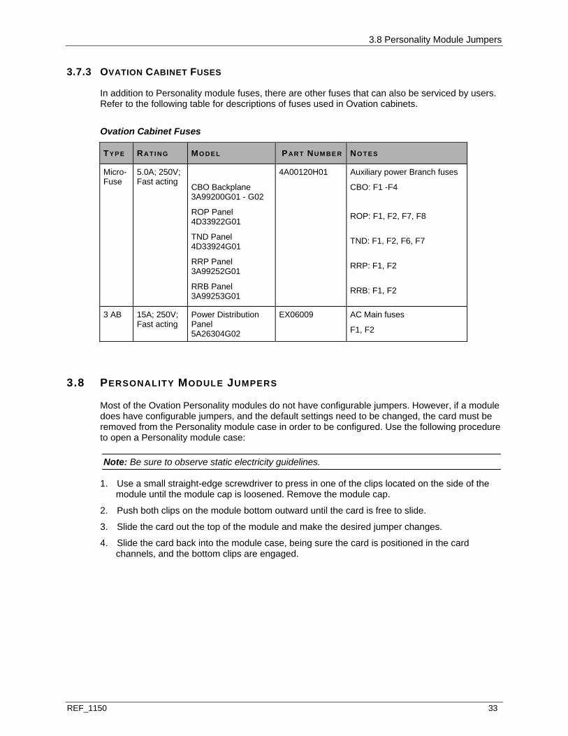
3.8 Personality Module Jumpers
REF_1150 33
3.7.3 OVATION CABINET FUSES
In addition to Personality module fuses, there are other fuses that can also be serviced by users. Refer to the following table for descriptions of fuses used in Ovation cabinets.
Ovation Cabinet Fuses
TYP E RAT I N G MO DE L PAR T NUM BE R NO T ES
Micro-Fuse
5.0A; 250V; Fast acting
CBO Backplane 3A99200G01 - G02
ROP Panel 4D33922G01
TND Panel 4D33924G01
RRP Panel 3A99252G01
RRB Panel 3A99253G01
4A00120H01 Auxiliary power Branch fuses
CBO: F1 -F4 ROP: F1, F2, F7, F8
TND: F1, F2, F6, F7
RRP: F1, F2
RRB: F1, F2
3 AB 15A; 250V; Fast acting
Power Distribution Panel 5A26304G02
EX06009 AC Main fuses
F1, F2
3.8 PERSONALITY MODULE JUMPERS
Most of the Ovation Personality modules do not have configurable jumpers. However, if a module does have configurable jumpers, and the default settings need to be changed, the card must be removed from the Personality module case in order to be configured. Use the following procedure to open a Personality module case:
Note: Be sure to observe static electricity guidelines.
1. Use a small straight-edge screwdriver to press in one of the clips located on the side of the module until the module cap is loosened. Remove the module cap.
2. Push both clips on the module bottom outward until the card is free to slide.
3. Slide the card out the top of the module and make the desired jumper changes.
4. Slide the card back into the module case, being sure the card is positioned in the card channels, and the bottom clips are engaged.
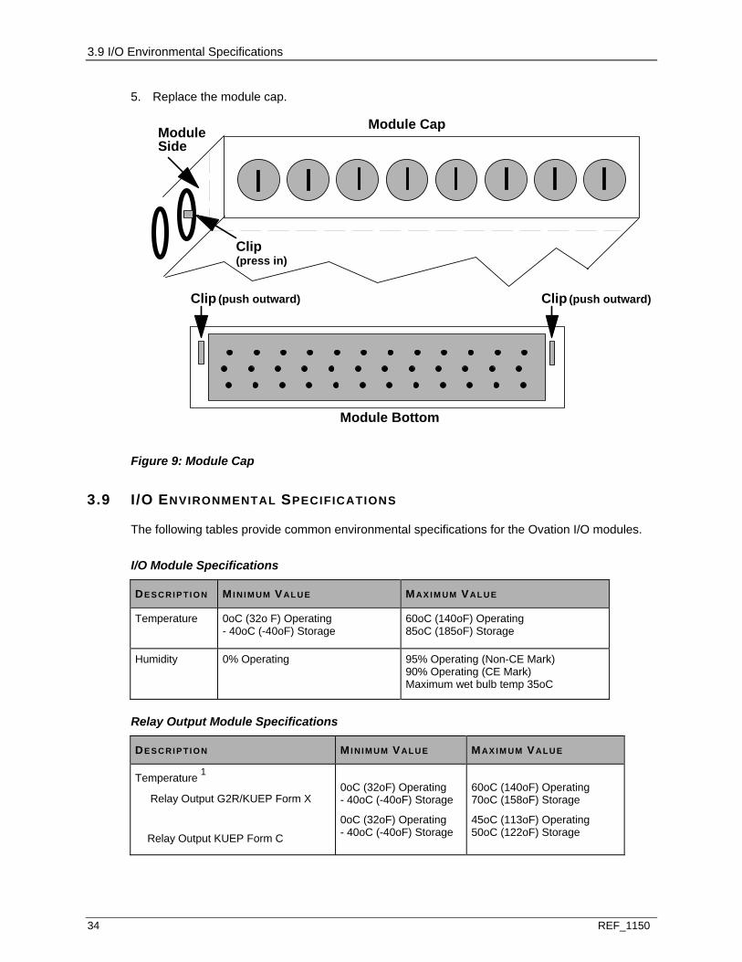
3.9 I/O Environmental Specifications
34 REF_1150
5. Replace the module cap.
Module Cap
Module Bottom
Clip (push outward)
Clip
ModuleSide
(press in)
Clip (push outward)
Figure 9: Module Cap
3.9 I/O ENVIRONMENTAL SPECIFICATIONS
The following tables provide common environmental specifications for the Ovation I/O modules.
I/O Module Specifications
DE S C RI P T I O N MI NI M UM VAL U E MAX I M UM VAL U E
Temperature
0oC (32o F) Operating - 40oC (-40oF) Storage
60oC (140oF) Operating 85oC (185oF) Storage
Humidity
0% Operating
95% Operating (Non-CE Mark) 90% Operating (CE Mark) Maximum wet bulb temp 35oC
Relay Output Module Specifications
DE S C RI P T I O N MI NI M UM VAL U E MAX I M UM VAL U E
Temperature 1
Relay Output G2R/KUEP Form X
Relay Output KUEP Form C
0oC (32oF) Operating - 40oC (-40oF) Storage
0oC (32oF) Operating - 40oC (-40oF) Storage
60oC (140oF) Operating 70oC (158oF) Storage
45oC (113oF) Operating 50oC (122oF) Storage
3.9 I/O Environmental Specifications
REF_1150 35
DE S C RI P T I O N MI NI M UM VAL U E MAX I M UM VAL U E
Humidity
Relay Output G2R
Relay Output KUEP Form X/Form C
35% Operating
N/A
85% Operating (Non-CE Mark)Maximum wet bulb temp 35oC
N/A
1 See Relay Output Module (see page 291) for additional temperature and derating information relative to specific cabinet configuration.


REF_1150 37
IN THIS SECTION
Description ........................................................................................................................ 37 Module Group Information ................................................................................................37 Module Specific Information..............................................................................................39 Wiring Information .............................................................................................................44 Address Location Information ...........................................................................................48 Diagnostic LEDs................................................................................................................52 Specifications .................................................................................................................... 53
4.1 DESCRIPTION
The Ovation Analog Input Module with associated Personality Module provides signal conditioning and analog-to-digital conversion for eight individually-isolated analog inputs. Field inputs are surge protected and routed by the appropriate Personality Module and then sent to the Electronics Module for conversion.
The Analog Input Module (13 bits) is applicable for CE Mark Certified Systems.
Note: I/O Module General Information (see page 15) contains environmental, installation, wiring, and fuse information for I/O modules.
4.2 MODULE GROUP INFORMATION
4.2.1 ELECTRONICS MODULES (EMODS)
There are six groups of Electronics modules for the Analog Input Module:
1C31113G01 provides voltage input range of ± 20 mV. 1C31113G02 provides voltage input range of ± 50 mV. 1C31113G03 provides voltage input range of ± 100 mV. 1C31113G04 provides voltage input range of ± 1 V. 1C31113G05 provides voltage input range of ± 5 V. 1C31113G06 provides voltage input range of ± 10 V.
S E C T I O N 4
ANALOG INPUT MODULE (13 BITS)
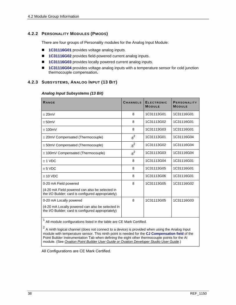
4.2 Module Group Information
38 REF_1150
4.2.2 PERSONALITY MODULES (PMODS)
There are four groups of Personality modules for the Analog Input Module:
1C31116G01 provides voltage analog inputs. 1C31116G02 provides field-powered current analog inputs. 1C31116G03 provides locally powered current analog inputs. 1C31116G04 provides voltage analog inputs with a temperature sensor for cold junction
thermocouple compensation.
4.2.3 SUBSYSTEMS, ANALOG INPUT (13 BIT)
Analog Input Subsystems (13 Bit)
RAN G E CH AN N E L S EL E C T RO NI C MO D U LE
PE R S O N AL I T Y MO D U LE
± 20mV 8 1C31113G01 1C31116G01
± 50mV 8 1C31113G02 1C31116G01
± 100mV 8 1C31113G03 1C31116G01
± 20mV Compensated (Thermocouple) 82 1C31113G01 1C31116G04
± 50mV Compensated (Thermocouple) 82 1C31113G02 1C31116G04
± 100mV Compensated (Thermocouple) 82 1C31113G03 1C31116G04
± 1 VDC 8 1C31113G04 1C31116G01
± 5 VDC 8 1C31113G05 1C31116G01
± 10 VDC 8 1C31113G06 1C31116G01
0-20 mA Field powered
(4-20 mA Field powered can also be selected in the I/O Builder; card is configured appropriately)
8 1C31113G05 1C31116G02
0-20 mA Locally powered
(4-20 mA Locally powered can also be selected in the I/O Builder; card is configured appropriately)
8 1C31113G05 1C31116G03
1 All module configurations listed in the table are CE Mark Certified. 2 A ninth logical channel (does not connect to a device) is provided when using the Analog Input module with temperature sensor. This ninth point is needed for the CJ Compensation field of the Point Builder Instrumentation Tab when defining the eight other thermocouple points for the AI module. (See Ovation Point Builder User Guide or Ovation Developer Studio User Guide.)
All Configurations are CE Mark Certified.
4.3 Module Specific Information
REF_1150 39
4.3 MODULE SPECIFIC INFORMATION
4.3.1 EXTERNAL POWER SUPPLIES
Note: Module power specifications (main and auxiliary) refer to the actual power drawn by the module from the 24VDC main power supply and from the auxiliary power supply (if required) and NOT from the AC or DC Mains.
If the Analog Input module uses the 1C31116G03 Personality module (configured with locally powered current analog inputs), the required voltage source may be obtained from the internal auxiliary power supply (backplane) or it may be obtained from an external power supply.
If an external power supply is used, Using an External Power Supply (see page 539) contains steps to be undertaken before connecting the external power supply to the Analog Input module base unit terminal block. The Analog Input module auxiliary supply voltage level (24 VDC or 48 VDC) depends on the external transmitter devices being interfaced to the Analog Input module’s analog inputs.

4.3 Module Specific Information
40 REF_1150
4.3.2 THERMOCOUPLE FUNCTION
When two dissimilar metals (a thermocouple) are joined together, a voltage (the Seebeck Voltage) is generated between them. This voltage is directly related to the temperature at the junction of the two metals. The relationship between the voltage and the temperature can be best described by a fifth order polynomial, determined by the two types of metals that are joined.
To measure the voltage (Vt) between the two metals, a voltmeter (in this case, an analog input card) must be connected to each wire. Unfortunately, this produces two new junctions and voltages (V1 and V2) between the terminals and the thermocouples. The following formula is used to find Vt: Vt = Vm -V1 -V2.
It is not possible to measure V1 and V2 without inducing more junctions and voltages; therefore, the analog input subsystem has a temperature sensor on the Personality module (1C31116G04) to measure the temperature (Tj) at the terminal block of the base unit.
A conversion formula, determined from the junction metal and thermocouple metals, is used to calculate the combined voltage of V1 and V2. This is called Cold Junction Compensation.
Figure 10: Thermocouple Illustration

4.3 Module Specific Information
REF_1150 41
Assigning Thermocouple Coefficients
Use the Instrumentation tab of the Point Builder to select the Field Instrumentation Type (B or TB, E or TE, J or TJ, K or TK, R or TR, S or TS, T or TT). The Ovation system then assigns the default thermocouple coefficients based on the Type selected. Refer to the following table for these coefficient definitions.
If you override the default coefficients by entering new values, the new values remain until you select another thermocouple type. The values then return to the values for the type just selected.
Thermocouple Coefficient Definitions
Thermocouple Type
Standard Temperature Range
Actual range in MV / TEMP Best Fit
B or TB 400 to 1100 Degrees C
800 to 2000 Degrees F
0.000 to 13.814 (0 to 1820)
0.006 to 13.814 (0 to 3308)
20 mv card
20 mv card
Fahrenheit
COEF_1 = 3.5164700E+02 COEF_2 = 6.1388490E+05 COEF_3 = – 1.5397740E+08 COEF_4 = 3.3593730E+10 COEF_5 = – 4.0518260E+12 COEF_6 = 2.0039330E+14 COEF_7 = – 2.0E-06 COEF_8 = 0.0
Centigrade
COEF_1 = 1.7758167E+02 COEF_2 = 3.4104717E+05 COEF_3 = – 8.5543000E+07 COEF_4 = – 8.5543000E+07 COEF_5 = – 8.5543000E+07 COEF_6 = 1.1132961E+14 COEF_7 = – 2.0E-06 COEF_8 = 0.0
E or TE – 18 to 286 Degrees C 0 to 550 Degrees F
– 18 to 661 Degrees C 0 to 1200 Degrees F
– 18 to 1000 Degrees C 0 to 1832 Degrees F
– 9.835 to 19.945 (– 270 to 286) – 9.835 to 19.945 (– 450 to 548)
– 9.835 to 49.992 (– 270 to 661) – 9.835 to 49.956 (– 450 to 1221)
– 9.835 to 76.358 (– 270 to 1000) – 9.835 to 76.358 (– 450 to 1832)
20 mv card 20 mv card
50 mv card 50 mv card
100 mv card 100 mv card
Fahrenheit
COEF_1 = 3.1672830E+01 COEF_2 = 3.0306280E+04 COEF_3 = – 3.3449490E+05 COEF_4 = 6.8495880E+06 COEF_5 = – 6.9753490E+07 COEF_6 = 2.9236530E0+08 COEF_7 = – 1.0939E-03 COEF_8 = 3.365E-05
Centigrade
COEF_1 = – 1.8176111E-01 COEF_2 = 1.6836822E+04 COEF_3 = – 1.8583050E+05 COEF_4 = 3.8053267E+06 COEF_5 = – 3.8751939E+07 COEF_6 = 1.6242517E+08 COEF_7 = – 1.71E-05 COEF_8 = 6.057E-05
J or TJ – 18 to 365 Degrees C – 140 to 700 Degrees F – 18 to 760 Degrees C – 140 to 1400 Degrees F
– 8.096 to 19.971 (– 210 to 366) – 8.137 to 19.977 (– 350 to 691) – 8.096 to 42.922 (– 210 to 760) – 8.137 to 42.922 (– 350 to 1400)
20 mv card 20 mv card 50 mv card 50 mv card

4.3 Module Specific Information
42 REF_1150
Thermocouple Type
Standard Temperature Range
Actual range in MV / TEMP Best Fit
Fahrenheit
COEF_1 = 3.112531E+01 COEF_2 = 3.6070270E+04 COEF_3 = – 4.2886170E+05 COEF_4 = 2.2613820E+07 COEF_5 = – 5.1743790E+08 COEF_6 = 3.9727830E+09 COEF_7 = – 9.256E-04 COEF_8 = 2.862E-05
Centigrade
COEF_1 = – 4.8593889E-01 COEF_2 = 2.0039039E+04 COEF_3 = – 2.3825650E+05 COEF_4 = 1.2563233E+07 COEF_5 = – 2.8746550E+08 COEF_6 = 2.2071017E+09 COEF_7 = – 9.76E-06 COEF_8 = 5.1516E-05
K or TK – 18 to 480 Degrees C 0 to 900 Degrees F
– 18 to 1230 Degrees C 0 to 2250 Degrees F
– 18 to 1370 Degrees C 0 to 2500 Degrees F
– 6.458 to 19.959 (– 270 to 484) – 6.456 to 19.978 (– 450 to 904)
– 6.458 to 49.988 (– 270 to 1232) – 6.456 to 49.996 (– 450 to 2250)
– 6.458 to 54.875 (– 270 to 1372) – 6.456 to 54.845 (– 450 to 2500)
20 mv card 20 mv card
50 mv card 50 mv card
100 mv card 100 mv card
Fahrenheit
COEF_1 = 3.0344730E+01 COEF_2 = 4.4031910E+04 COEF_3 = 1.615839E+05 COEF_4 = – 1.616257E+07 COEF_5 = 4.4011090E+08 COEF_6 = – 3.599650E+09 COEF_7 = – 7.259E-04 COEF_8 = 2.243E-05
Centigrade
COEF_1 = – 9.1959444E-01 COEF_2 = 2.4462172E+04 COEF_3 = 8.9768833E+04 COEF_4 = – 8.9792056E+06 COEF_5 = 2.4450606E+08 COEF_6 = – 1.9998056E+09 COEF_7 = – 8.14E-06 COEF_8 = 4.0374E-05
R or TR 260 to 1100 Degrees C 500 to 2000 Degrees F
0.000 to 19.998 (0 to 1684) 0.089 to 19.997 (0 to 3063)
20 mv card 20 mv card
Fahrenheit
COEF_1 = 8.3628480E+01 COEF_2 = 2.2737160E+05 COEF_3 = – 1.2482860E+07 COEF_4 = 1.2062540E+09 COEF_5 = – 7.4221280E+10 COEF_6 = 1.89930000E+12 COEF_7 = – 1.084E-04 COEF_8 = 3.24E-06
Centigrade
COEF_1 = 2.8682489E+01 COEF_2 = 1.2631756E+05 COEF_3 = – 6.9349222E+06 COEF_4 = 6.7014111E+08 COEF_5 = – 4.1234044E+10 COEF_6 = 1.0551667E+12 COEF_7 = – 4.72E-06 COEF_8 = 5.832E-06
S or TS 400 to 1100 Degrees C 750 to 2000 Degrees F
0.000 to 18.698 (0 to 1768) -0.092 to 18.696 (0 to 3214)
20 mv card 20 mv card
Fahrenheit
COEF_1 = 1.1803440E+02 COEF_2 = 1.9859180E+05 COEF_3 = – 1.9730960E+04 COEF_4 = – 5.0093290E+08 COEF_5 = 4.1104880E+10 COEF_6 = – 1.1557940E+12 COEF_7 = – 1.0847E-04 COEF_8 = 3.26E-06
Centigrade
COEF_1 = 4.7796889E+01 COEF_2 = 1.1032878E+05 COEF_3 = – 1.0961644E+04 COEF_4 = – 2.7829606E+08 COEF_5 = 2.2836044E+10 COEF_6 = – 6.4210778E+11 COEF_7 = – 4.15E-06 COEF_8 = 5.868E-06
T or TT -46 to 400 Degrees C -50 to 750 Degrees F
-6.258 to 19.945 (-270 to 385) -6.254 to 19.979 (-450 to 726)
20 mv card 20 mv card
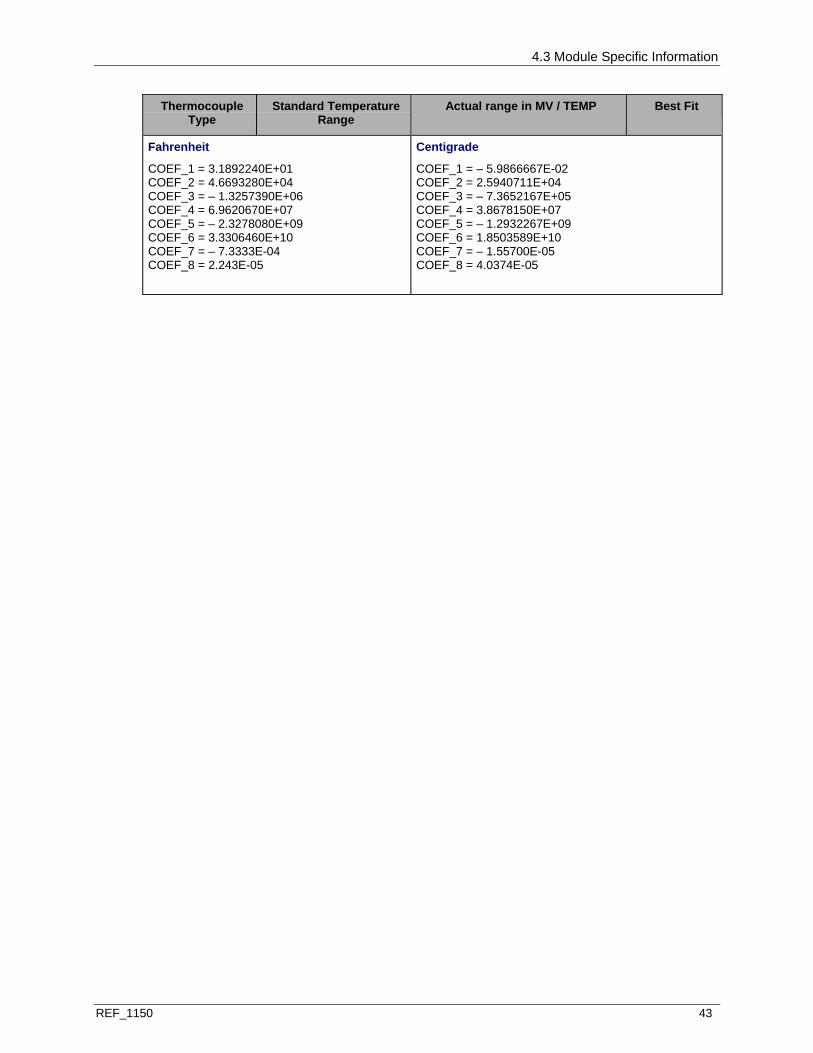
4.3 Module Specific Information
REF_1150 43
Thermocouple Type
Standard Temperature Range
Actual range in MV / TEMP Best Fit
Fahrenheit
COEF_1 = 3.1892240E+01 COEF_2 = 4.6693280E+04 COEF_3 = – 1.3257390E+06 COEF_4 = 6.9620670E+07 COEF_5 = – 2.3278080E+09 COEF_6 = 3.3306460E+10 COEF_7 = – 7.3333E-04 COEF_8 = 2.243E-05
Centigrade
COEF_1 = – 5.9866667E-02 COEF_2 = 2.5940711E+04 COEF_3 = – 7.3652167E+05 COEF_4 = 3.8678150E+07 COEF_5 = – 1.2932267E+09 COEF_6 = 1.8503589E+10 COEF_7 = – 1.55700E-05 COEF_8 = 4.0374E-05
4.4 Wiring Information
44 REF_1150
4.4 WIRING INFORMATION
4.4.1 13-BIT ANALOG INPUT TERMINAL BLOCK WIRING INFORMATION
Each Personality module has a simplified wiring diagram label on its side, which appears above the terminal block. This diagram indicates how the wiring from the field is to be connected to the terminal block in the base unit.
The diagrams for the analog input Personality modules are illustrated in the following figure. The following table lists and defines the abbreviations used in those diagrams.
Figure 11: Terminal Block Connections for the Analog Input Personality Modules
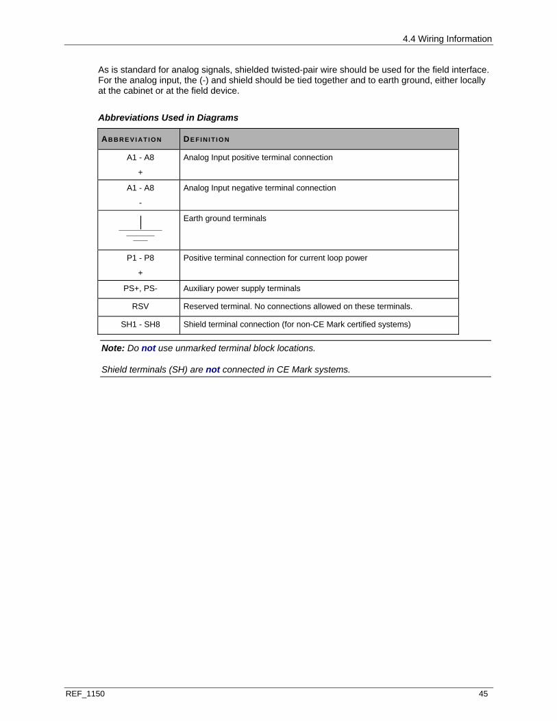
4.4 Wiring Information
REF_1150 45
As is standard for analog signals, shielded twisted-pair wire should be used for the field interface. For the analog input, the (-) and shield should be tied together and to earth ground, either locally at the cabinet or at the field device.
Abbreviations Used in Diagrams
AB B R E V I AT I ON DE FI N I T I O N
A1 - A8
+
Analog Input positive terminal connection
A1 - A8
-
Analog Input negative terminal connection
Earth ground terminals
P1 - P8
+
Positive terminal connection for current loop power
PS+, PS- Auxiliary power supply terminals
RSV Reserved terminal. No connections allowed on these terminals.
SH1 - SH8 Shield terminal connection (for non-CE Mark certified systems)
Note: Do not use unmarked terminal block locations.
Shield terminals (SH) are not connected in CE Mark systems.
4.4 Wiring Information
46 REF_1150
4.4.2 13-BIT ANALOG INPUT FIELD CONNECTION WIRING DIAGRAMS (NON-CE MARK CERTIFIED)
Figure 12: Field Connections, Analog Input Personality Module (Non-CE Mark)
Note: See Personality Module Jumpers (see page 33) for details on accessing the jumpers.

4.4 Wiring Information
REF_1150 47
4.4.3 13-BIT ANALOG INPUT FIELD CONNECTION WIRING DIAGRAMS (CE MARK CERTIFIED)
Figure 13: Field Connections for the Analog Input Personality Module (CE Mark)
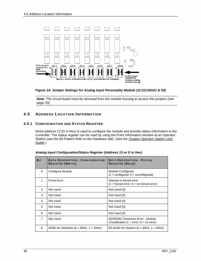
4.5 Address Location Information
48 REF_1150
Figure 14: Jumper Settings for Analog Input Personality Module (1C31116G01 & 04)
Note: The circuit board must be removed from the module housing to access the jumpers (see page 33).
4.5 ADDRESS LOCATION INFORMATION
4.5.1 CONFIGURATION AND STATUS REGISTER
Word address 13 (D in Hex) is used to configure the module and provide status information to the Controller. The status register can be read by using the Point Information window at an Operator Station (see the Bit Pattern field on the Hardware tab). (See the Ovation Operator Station User Guide.)
Analog Input Configuration/Status Register (Address 13 or D in Hex)
BI T DAT A DE S C R I P T I O N - CO NF I G U R AT I O N RE GI S T E R (WRI T E)
DAT A DE S C R I P T I O N - ST AT U S RE GI S T E R (RE AD)
0 Configure Module Module Configured (1 = configured; 0 = unconfigured)
1 Force Error Internal or forced error (1 = forced error; 0 = no forced error)
2 Not Used Not Used (0)
3 Not Used Not Used (0)
4 Not Used Not Used (0)
5 Not Used Not Used (0)
6 Not Used Not Used (0)
7 Not Used EEPROM Checksum Error - Module Uncalibrated (1 = error; 0 = no error)
8 50/60 Hz Selection (0 = 60Hz, 1 = 50Hz) 50 Hz/60 Hz System (0 = 60Hz; 1 = 50Hz)
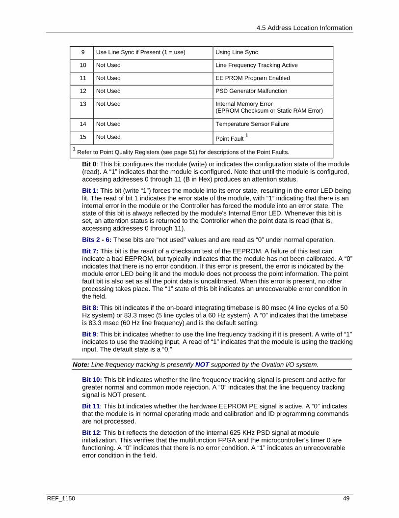
4.5 Address Location Information
REF_1150 49
9 Use Line Sync if Present (1 = use) Using Line Sync
10 Not Used Line Frequency Tracking Active
11 Not Used EE PROM Program Enabled
12 Not Used PSD Generator Malfunction
13 Not Used Internal Memory Error (EPROM Checksum or Static RAM Error)
14 Not Used Temperature Sensor Failure
15 Not Used Point Fault 1 1 Refer to Point Quality Registers (see page 51) for descriptions of the Point Faults.
Bit 0: This bit configures the module (write) or indicates the configuration state of the module (read). A “1” indicates that the module is configured. Note that until the module is configured, accessing addresses 0 through 11 (B in Hex) produces an attention status.
Bit 1: This bit (write “1”) forces the module into its error state, resulting in the error LED being lit. The read of bit 1 indicates the error state of the module, with “1” indicating that there is an internal error in the module or the Controller has forced the module into an error state. The state of this bit is always reflected by the module's Internal Error LED. Whenever this bit is set, an attention status is returned to the Controller when the point data is read (that is, accessing addresses 0 through 11).
Bits 2 - 6: These bits are “not used” values and are read as “0” under normal operation.
Bit 7: This bit is the result of a checksum test of the EEPROM. A failure of this test can indicate a bad EEPROM, but typically indicates that the module has not been calibrated. A “0” indicates that there is no error condition. If this error is present, the error is indicated by the module error LED being lit and the module does not process the point information. The point fault bit is also set as all the point data is uncalibrated. When this error is present, no other processing takes place. The “1” state of this bit indicates an unrecoverable error condition in the field.
Bit 8: This bit indicates if the on-board integrating timebase is 80 msec (4 line cycles of a 50 Hz system) or 83.3 msec (5 line cycles of a 60 Hz system). A “0” indicates that the timebase is 83.3 msec (60 Hz line frequency) and is the default setting.
Bit 9: This bit indicates whether to use the line frequency tracking if it is present. A write of “1” indicates to use the tracking input. A read of “1” indicates that the module is using the tracking input. The default state is a “0.”
Note: Line frequency tracking is presently NOT supported by the Ovation I/O system.
Bit 10: This bit indicates whether the line frequency tracking signal is present and active for greater normal and common mode rejection. A “0” indicates that the line frequency tracking signal is NOT present.
Bit 11: This bit indicates whether the hardware EEPROM PE signal is active. A “0” indicates that the module is in normal operating mode and calibration and ID programming commands are not processed.
Bit 12: This bit reflects the detection of the internal 625 KHz PSD signal at module initialization. This verifies that the multifunction FPGA and the microcontroller's timer 0 are functioning. A “0” indicates that there is no error condition. A “1” indicates an unrecoverable error condition in the field.
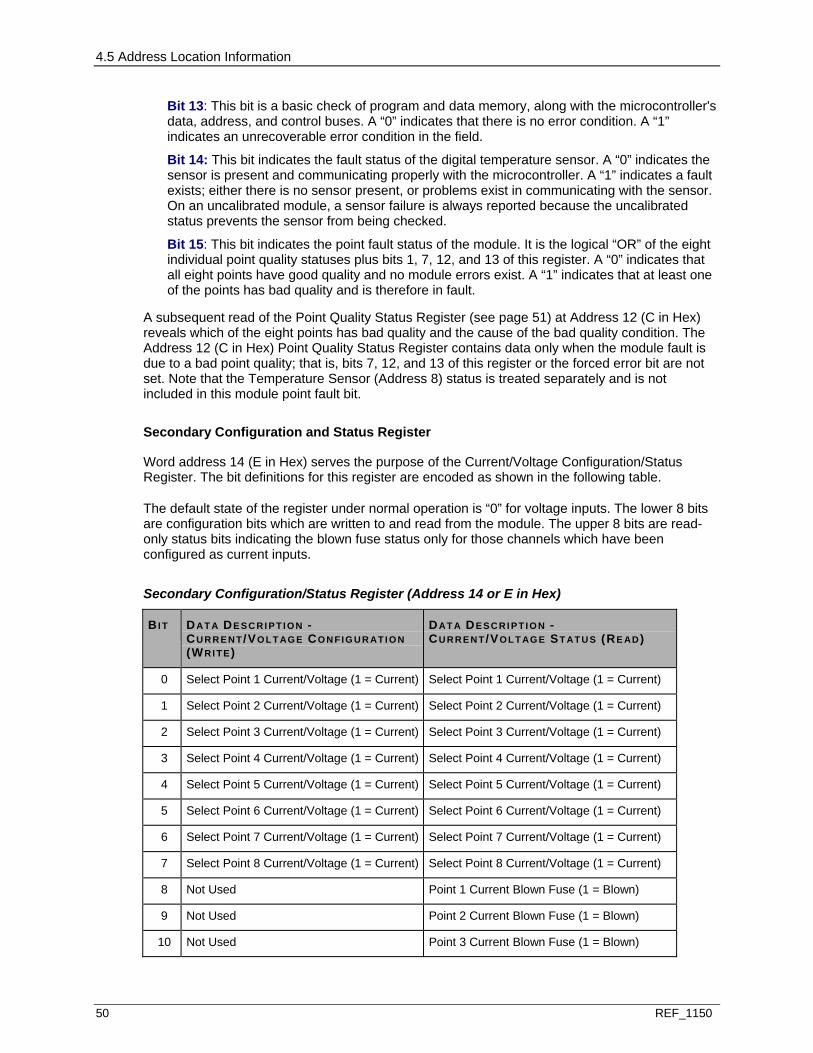
4.5 Address Location Information
50 REF_1150
Bit 13: This bit is a basic check of program and data memory, along with the microcontroller's data, address, and control buses. A “0” indicates that there is no error condition. A “1” indicates an unrecoverable error condition in the field.
Bit 14: This bit indicates the fault status of the digital temperature sensor. A “0” indicates the sensor is present and communicating properly with the microcontroller. A “1” indicates a fault exists; either there is no sensor present, or problems exist in communicating with the sensor. On an uncalibrated module, a sensor failure is always reported because the uncalibrated status prevents the sensor from being checked.
Bit 15: This bit indicates the point fault status of the module. It is the logical “OR” of the eight individual point quality statuses plus bits 1, 7, 12, and 13 of this register. A “0” indicates that all eight points have good quality and no module errors exist. A “1” indicates that at least one of the points has bad quality and is therefore in fault.
A subsequent read of the Point Quality Status Register (see page 51) at Address 12 (C in Hex) reveals which of the eight points has bad quality and the cause of the bad quality condition. The Address 12 (C in Hex) Point Quality Status Register contains data only when the module fault is due to a bad point quality; that is, bits 7, 12, and 13 of this register or the forced error bit are not set. Note that the Temperature Sensor (Address 8) status is treated separately and is not included in this module point fault bit.
Secondary Configuration and Status Register
Word address 14 (E in Hex) serves the purpose of the Current/Voltage Configuration/Status Register. The bit definitions for this register are encoded as shown in the following table.
The default state of the register under normal operation is “0” for voltage inputs. The lower 8 bits are configuration bits which are written to and read from the module. The upper 8 bits are read-only status bits indicating the blown fuse status only for those channels which have been configured as current inputs.
Secondary Configuration/Status Register (Address 14 or E in Hex)
BI T DAT A DE S C R I P T I O N - CU R R E N T/VOLT AG E CO N FI G U R AT I O N (WRI TE)
DAT A DE S C R I P T I O N - CU R R E N T/VO L T AG E ST AT U S (RE AD)
0 Select Point 1 Current/Voltage (1 = Current) Select Point 1 Current/Voltage (1 = Current)
1 Select Point 2 Current/Voltage (1 = Current) Select Point 2 Current/Voltage (1 = Current)
2 Select Point 3 Current/Voltage (1 = Current) Select Point 3 Current/Voltage (1 = Current)
3 Select Point 4 Current/Voltage (1 = Current) Select Point 4 Current/Voltage (1 = Current)
4 Select Point 5 Current/Voltage (1 = Current) Select Point 5 Current/Voltage (1 = Current)
5 Select Point 6 Current/Voltage (1 = Current) Select Point 6 Current/Voltage (1 = Current)
6 Select Point 7 Current/Voltage (1 = Current) Select Point 7 Current/Voltage (1 = Current)
7 Select Point 8 Current/Voltage (1 = Current) Select Point 8 Current/Voltage (1 = Current)
8 Not Used Point 1 Current Blown Fuse (1 = Blown)
9 Not Used Point 2 Current Blown Fuse (1 = Blown)
10 Not Used Point 3 Current Blown Fuse (1 = Blown)
4.5 Address Location Information
REF_1150 51
11 Not Used Point 4 Current Blown Fuse (1 = Blown)
12 Not Used Point 5 Current Blown Fuse (1 = Blown)
13 Not Used Point 6 Current Blown Fuse (1 = Blown)
14 Not Used Point 7 Current Blown Fuse (1 = Blown)
15 Not Used Point 8 Current Blown Fuse (1 = Blown)
Point Quality Register
Word address 12 (C in Hex) serves the purpose of reporting the point quality of the eight channel inputs. The bit definitions for this register are encoded as shown in the following table.
Point Quality Register (Address 12 or C in Hex)
Point Bit Description
1 0 Auto Calibration Reasonability Check Failed
1 Overrange Input/Blown Fuse/Open Loop/Open Thermocouple
2 2 Auto Calibration Reasonability Check Failed
3 Overrange Input/Blown Fuse/Open Loop/Open Thermocouple
3 4 Auto Calibration Reasonability Check Failed
5 Overrange Input/Blown Fuse/Open Loop/Open Thermocouple
4 6 Auto Calibration Reasonability Check Failed
7 Overrange Input/Blown Fuse/Open Loop/Open Thermocouple
5 8 Auto Calibration Reasonability Check Failed
9 Overrange Input/Blown Fuse/Open Loop/Open Thermocouple
6 10 Auto Calibration Reasonability Check Failed
11 Overrange Input/Blown Fuse/Open Loop/Open Thermocouple
7 12 Auto Calibration Reasonability Check Failed
13 Overrange Input/Blown Fuse/Open Loop/Open Thermocouple
8 14 Auto Calibration Reasonability Check Failed
15 Overrange Input/Blown Fuse/Open Loop/Open Thermocouple
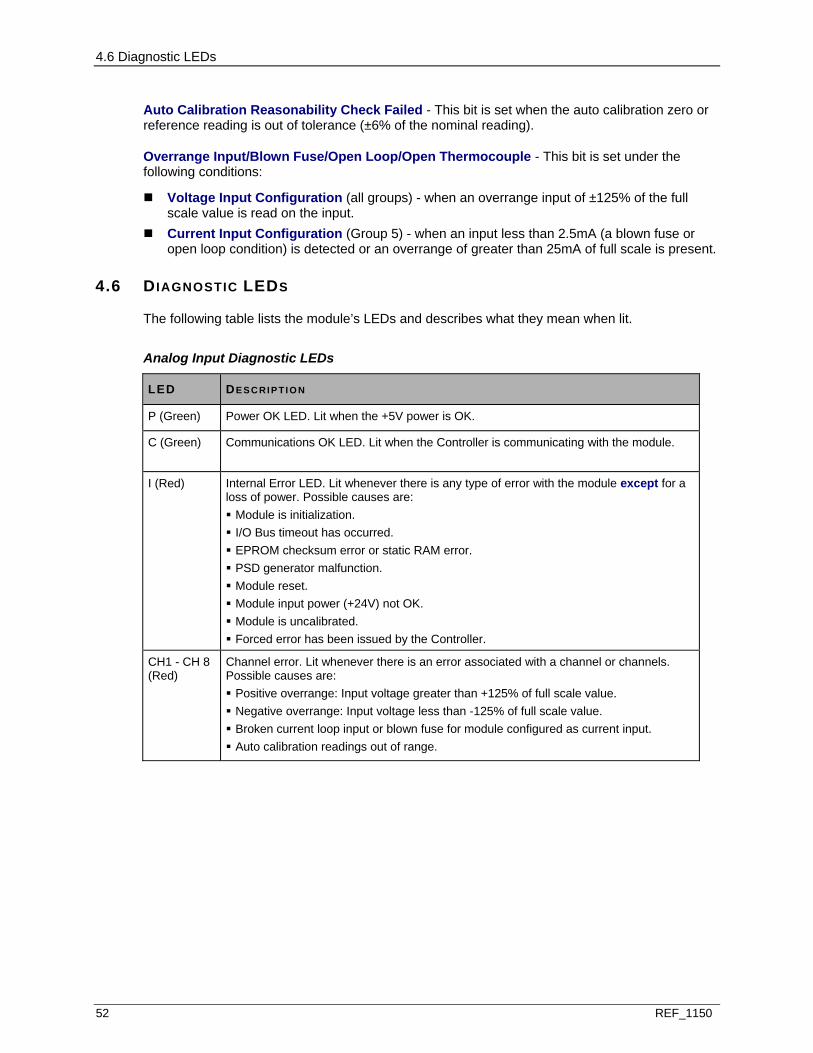
4.6 Diagnostic LEDs
52 REF_1150
Auto Calibration Reasonability Check Failed - This bit is set when the auto calibration zero or reference reading is out of tolerance (±6% of the nominal reading).
Overrange Input/Blown Fuse/Open Loop/Open Thermocouple - This bit is set under the following conditions:
Voltage Input Configuration (all groups) - when an overrange input of ±125% of the full scale value is read on the input.
Current Input Configuration (Group 5) - when an input less than 2.5mA (a blown fuse or open loop condition) is detected or an overrange of greater than 25mA of full scale is present.
4.6 DIAGNOSTIC LEDS
The following table lists the module’s LEDs and describes what they mean when lit.
Analog Input Diagnostic LEDs
LED DE S C RI P T I O N
P (Green) Power OK LED. Lit when the +5V power is OK.
C (Green) Communications OK LED. Lit when the Controller is communicating with the module.
I (Red) Internal Error LED. Lit whenever there is any type of error with the module except for a loss of power. Possible causes are: Module is initialization. I/O Bus timeout has occurred. EPROM checksum error or static RAM error. PSD generator malfunction. Module reset. Module input power (+24V) not OK. Module is uncalibrated. Forced error has been issued by the Controller.
CH1 - CH 8 (Red)
Channel error. Lit whenever there is an error associated with a channel or channels. Possible causes are: Positive overrange: Input voltage greater than +125% of full scale value. Negative overrange: Input voltage less than -125% of full scale value. Broken current loop input or blown fuse for module configured as current input. Auto calibration readings out of range.
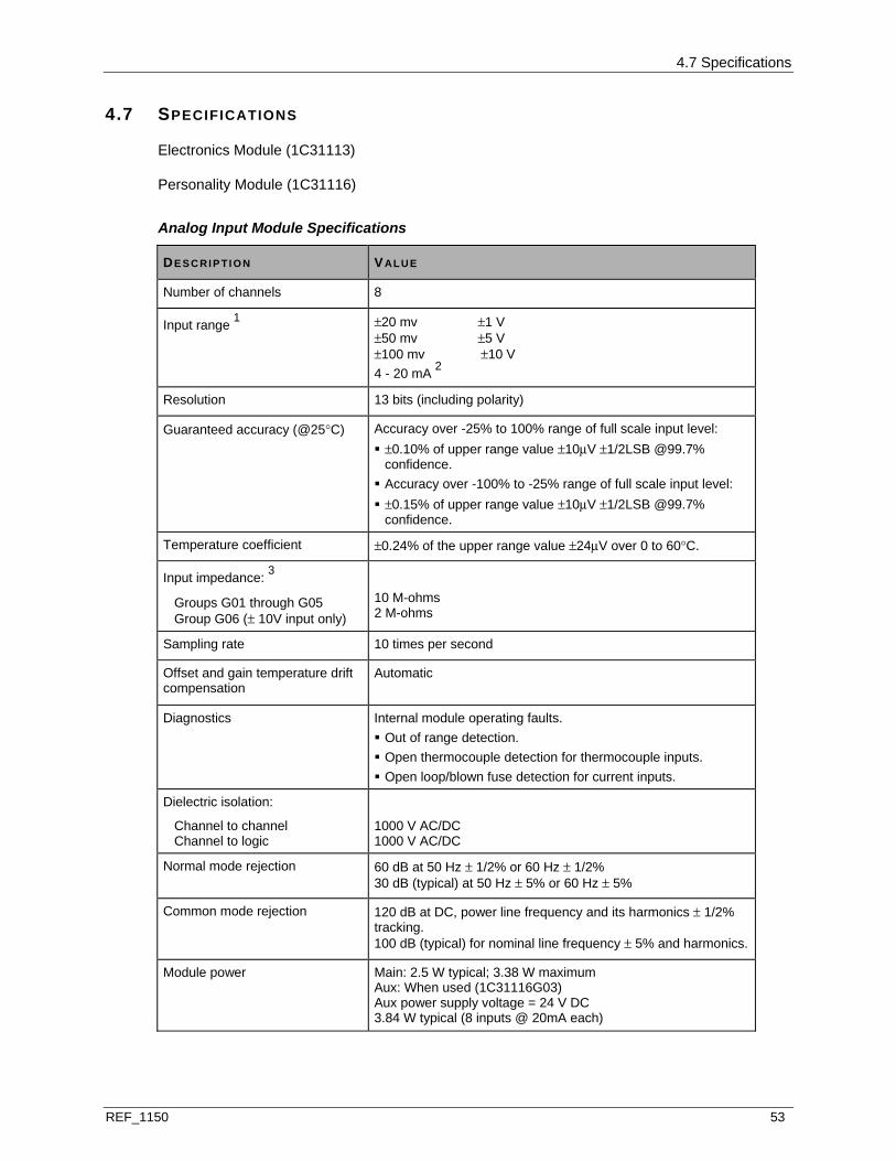
4.7 Specifications
REF_1150 53
4.7 SPECIFICATIONS
Electronics Module (1C31113)
Personality Module (1C31116)
Analog Input Module Specifications
DE S C RI P T I O N VAL U E
Number of channels 8
Input range 1 ±20 mv ±1 V ±50 mv ±5 V ±100 mv ±10 V 4 - 20 mA 2
Resolution 13 bits (including polarity)
Guaranteed accuracy (@25°C) Accuracy over -25% to 100% range of full scale input level: ±0.10% of upper range value ±10μV ±1/2LSB @99.7% confidence.
Accuracy over -100% to -25% range of full scale input level: ±0.15% of upper range value ±10μV ±1/2LSB @99.7% confidence.
Temperature coefficient ±0.24% of the upper range value ±24μV over 0 to 60°C.
Input impedance: 3
Groups G01 through G05 Group G06 (± 10V input only)
10 M-ohms 2 M-ohms
Sampling rate 10 times per second
Offset and gain temperature drift compensation
Automatic
Diagnostics Internal module operating faults. Out of range detection. Open thermocouple detection for thermocouple inputs. Open loop/blown fuse detection for current inputs.
Dielectric isolation:
Channel to channel Channel to logic
1000 V AC/DC 1000 V AC/DC
Normal mode rejection 60 dB at 50 Hz ± 1/2% or 60 Hz ± 1/2% 30 dB (typical) at 50 Hz ± 5% or 60 Hz ± 5%
Common mode rejection 120 dB at DC, power line frequency and its harmonics ± 1/2% tracking. 100 dB (typical) for nominal line frequency ± 5% and harmonics.
Module power Main: 2.5 W typical; 3.38 W maximum Aux: When used (1C31116G03) Aux power supply voltage = 24 V DC 3.84 W typical (8 inputs @ 20mA each)
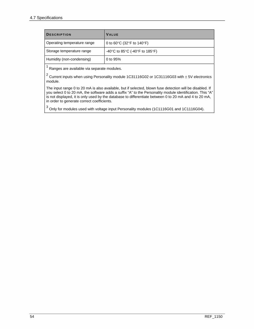
4.7 Specifications
54 REF_1150
DE S C RI P T I O N VAL U E
Operating temperature range 0 to 60°C (32°F to 140°F)
Storage temperature range -40°C to 85°C (-40°F to 185°F)
Humidity (non-condensing) 0 to 95%
1 Ranges are available via separate modules. 2 Current inputs when using Personality module 1C31116G02 or 1C31116G03 with ± 5V electronics module.
The input range 0 to 20 mA is also available, but if selected, blown fuse detection will be disabled. If you select 0 to 20 mA, the software adds a suffix “A” to the Personality module identification. This “A” is not displayed, it is only used by the database to differentiate between 0 to 20 mA and 4 to 20 mA, in order to generate correct coefficients. 3 Only for modules used with voltage input Personality modules (1C1116G01 and 1C1116G04).

REF_1150 55
IN THIS SECTION
Description ........................................................................................................................ 55 Module Group Information ................................................................................................55 Module Specific Information..............................................................................................56 Wiring Information .............................................................................................................57 Address Location Information ...........................................................................................60 Diagnostic LEDs................................................................................................................63 Specifications .................................................................................................................... 64
5.1 DESCRIPTION
The combined Personality and Electronics Modules form the 14 Bit Analog Input Module. Eight sets of individually isolated input channels are provided. The input signals are conditioned and routed through the appropriate Personality Module to the Electronics Module. The Personality Module also provides surge protection to protect the input circuits of the Electronics Module. The Electronics Module performs the analog to digital conversions and provides interfacing to the Ovation Serial I/O Bus.
No thermocouple provisions are provided for this module.
Note: I/O Module General Information (see page 15) contains environmental, installation, wiring, and fuse information for I/O modules.
5.2 MODULE GROUP INFORMATION
5.2.1 ELECTRONICS MODULES (EMODS)
There are two groups of Electronics modules for the 14 Bit Analog Input Module:
1C31224G01 provides current signals with an input range of 4 to 20 mA. 1C31224G02 provides voltage signals with an input range of ± 1V.
5.2.2 PERSONALITY MODULES (PMODS)
There are two groups of Personality modules for the 14 Bit Analog Input Module:
1C31227G01 provides current signals with an input range of 4 to 20 mA. 1C31227G02 provides voltage signals with an input range of ± 1V.
S E C T I O N 5
ANALOG INPUT MODULE (14 BITS)
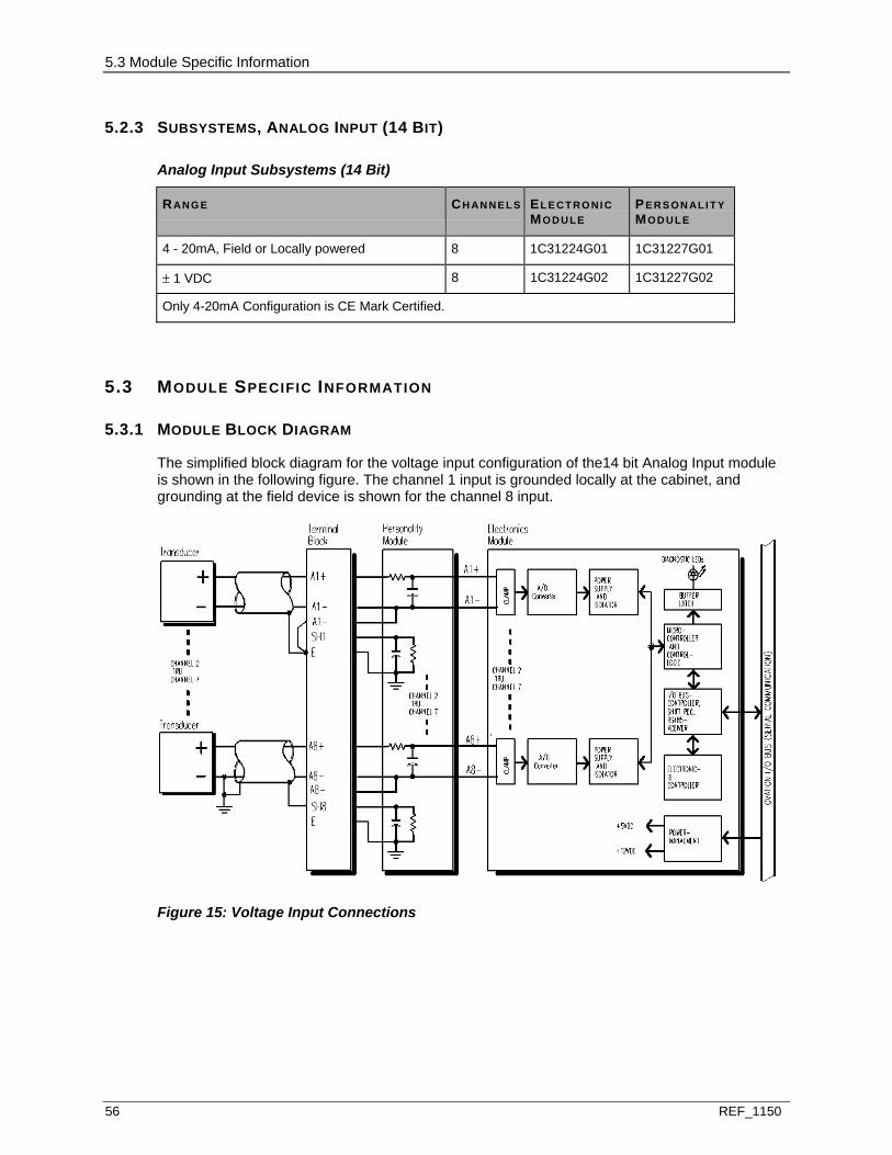
5.3 Module Specific Information
56 REF_1150
5.2.3 SUBSYSTEMS, ANALOG INPUT (14 BIT)
Analog Input Subsystems (14 Bit)
RAN G E CH AN N E L S EL E C T RO NI C MO D U LE
PE R S O N AL I T Y MO D U LE
4 - 20mA, Field or Locally powered 8 1C31224G01 1C31227G01
± 1 VDC 8 1C31224G02 1C31227G02
Only 4-20mA Configuration is CE Mark Certified.
5.3 MODULE SPECIFIC INFORMATION
5.3.1 MODULE BLOCK DIAGRAM
The simplified block diagram for the voltage input configuration of the14 bit Analog Input module is shown in the following figure. The channel 1 input is grounded locally at the cabinet, and grounding at the field device is shown for the channel 8 input.
Figure 15: Voltage Input Connections
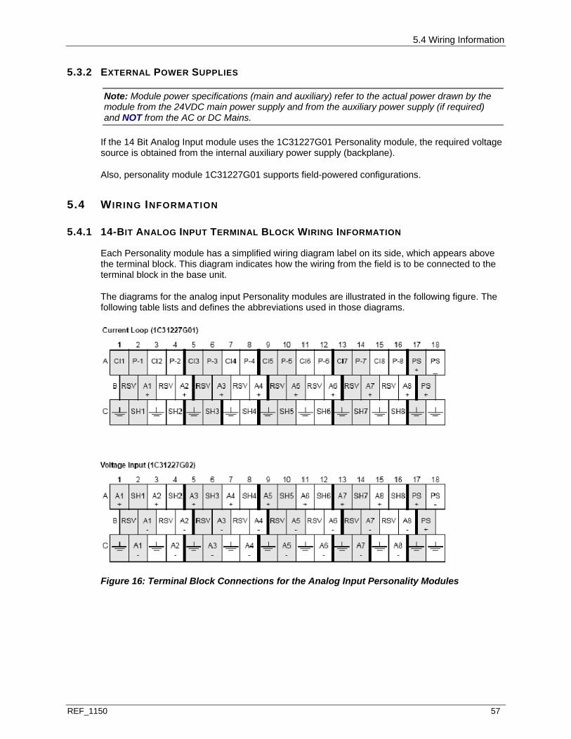
5.4 Wiring Information
REF_1150 57
5.3.2 EXTERNAL POWER SUPPLIES
Note: Module power specifications (main and auxiliary) refer to the actual power drawn by the module from the 24VDC main power supply and from the auxiliary power supply (if required) and NOT from the AC or DC Mains.
If the 14 Bit Analog Input module uses the 1C31227G01 Personality module, the required voltage source is obtained from the internal auxiliary power supply (backplane).
Also, personality module 1C31227G01 supports field-powered configurations.
5.4 WIRING INFORMATION
5.4.1 14-BIT ANALOG INPUT TERMINAL BLOCK WIRING INFORMATION
Each Personality module has a simplified wiring diagram label on its side, which appears above the terminal block. This diagram indicates how the wiring from the field is to be connected to the terminal block in the base unit.
The diagrams for the analog input Personality modules are illustrated in the following figure. The following table lists and defines the abbreviations used in those diagrams.
Figure 16: Terminal Block Connections for the Analog Input Personality Modules

5.4 Wiring Information
58 REF_1150
Abbreviations Used in Diagrams
AB B R E V I AT I ON DE FI N I T I O N
A1 - A8
+
Analog Input positive terminal connection (connected to the positive terminal of the field device).
A1 - A8
-
Analog Input negative terminal connection (voltage input group only).
P-1 - P-8 Loop power output terminals (for locally powered loops).
CI1 - CI8 Current input terminals.
SH1 - SH8 Shield terminal connection.
RSV Reserved terminal. No connections allowed on these terminals.
Earth ground terminals.
PS+, PS- Auxiliary power supply terminals.
Use shielded twisted pair wire for the field wiring. Tie the Analog Input negative terminal and shield together and to earth ground, either locally at the cabinet or at the field device. Voltage inputs use the 1C31227G02 Personality Modules. Grounding the shield and the analog input negative terminal at the cabinet or at the field device is arranged by the proper Terminal Block connections.
Similarly, current inputs using the 1C31227G01 Personality Modules can accommodate field or locally powered devices by using the correct terminal block connections.
The Personality Modules have a field connection diagram label on top of each module to facilitate field wiring. The figures in 14-Bit Analog Input Field Connection Wiring Diagrams (Non-CE Mark Certified) (see page 59) show the implementations of the field connections for the various Personality Module and field device combinations.
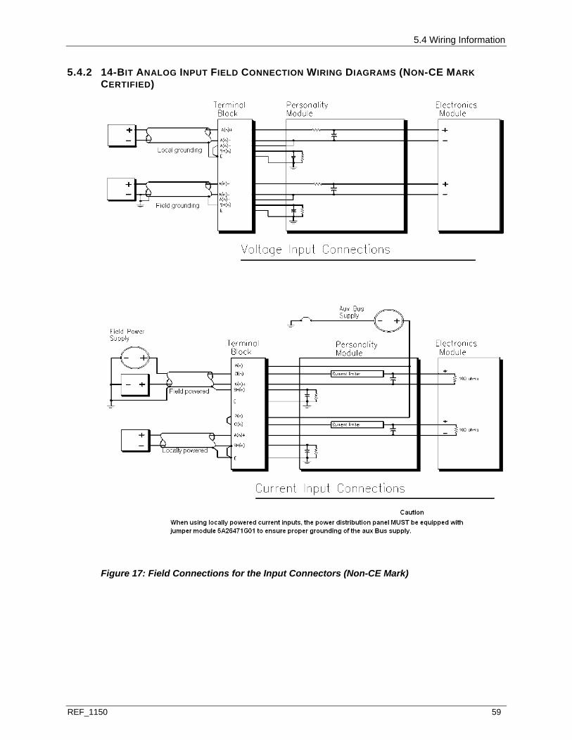
5.4 Wiring Information
REF_1150 59
5.4.2 14-BIT ANALOG INPUT FIELD CONNECTION WIRING DIAGRAMS (NON-CE MARK CERTIFIED)
Figure 17: Field Connections for the Input Connectors (Non-CE Mark)

5.5 Address Location Information
60 REF_1150
5.4.3 14-BIT ANALOG INPUT FIELD CONNECTION WIRING DIAGRAMS (CE MARK CERTIFIED)
Figure 18: Field Connections for the Input Connectors (CE Mark)
5.5 ADDRESS LOCATION INFORMATION
5.5.1 CONFIGURATION AND STATUS REGISTER
Word address 13 (D in Hex) is used to configure the module and provide status information to the Controller. The status register can be read by using the Point Information window at an Operator Station (See the Operator Station User Guide).
14-Bit Analog Input Configuration/Status (Address 13 or D in Hex)
BI T DAT A DE S C R I P T I O N - CO N FI G U R AT I O N REGI S TE R (WRI TE)
DAT A DE S C R I P T I O N - ST AT U S REGI S TER (RE AD)
0 Configure Module Module Configured
(1 = configured; 0 = unconfigured)
1 Force Error Internal or forced error
(1 = forced error; 0 = no forced error)
2 0, (ADD4 bit during diagnostics) Not Used (0)
3 0, (ADD5 bit during diagnostics) Not Used (0)
4 0, (ADD6 bit during diagnostics) Warming
5 0, (ADD7 bit during diagnostics) Not Used (0)

5.5 Address Location Information
REF_1150 61
BI T DAT A DE S C R I P T I O N - CO N FI G U R AT I O N REGI S TE R (WRI TE)
DAT A DE S C R I P T I O N - ST AT U S REGI S TER (RE AD)
6 0, (ADD8 bit during diagnostics) Not Used (0)
7 0, (DIAG_SET, initiates diagnostics) Module is not calibrated
8 50/60 Hz Selection (0 = 60Hz, 1 = 50Hz) 50 Hz/60 Hz System (0 = 60Hz; 1 = 50Hz)
9 A/D conversion rate selection bit
(0 = Normal, 1 = High speed)
A/D conversion rate bit
(0 = Normal, 1 = High speed)
10 0, (SYS_CAL, initiates system calibration during diagnostics)
SYS_CAL in progress (during diagnostics)
11 SELF_CAL (initiates self calibration) SYS_CAL completed (during diagnostics)
12 Not defined SYS_CAL failed (during diagnostics)
13 Not defined Internal Memory Error
(FLASH Checksum, Register, or Static RAM Error)
14 Not defined Module in diagnostic mode (during diagnostics)
15 Not defined Point Fault 1
1 Refer to the Point Quality Register for descriptions of the Point Faults.
Bits defined for diagnostics are used only during factory testing.
Bit 0: This bit configures the module (write) or indicates the configuration state of the module (read). A “1” indicates that the module is configured. Note that until the module is configured, reading from addresses 0 through 11 (B in Hex) produces an attention status.
Bit 1: This bit (write “1”) forces the module into its error state, resulting in the error LED being lit. The read of bit 1 indicates that there is an internal module error, or the Controller has forced the module into the error state. The state of this bit is always reflected by the module's Internal Error LED. Whenever this bit is set, an attention status is returned to the Controller when addresses 0 through 11 (B in Hex) are read.
Bits 2-3: These bits are not used and are read as “0” under normal operation.
Bit 4: This bit (read) indicates that the module is in the “Warming” state. This state exists after power up and terminates after 8.16 seconds. The module is in the error condition during the warm up period.
Bits 5-6: These bits are not used and are read as “0” under normal operation.
Bit 7: This bit is the result of a checksum test of the EEPROM. A failure of this test can indicate a bad EEPROM, but typically indicates that the module has not been calibrated. A “0” indicates that there is no error condition. If an error is present, the error is indicated by the module error LED being lit. The point fault bit is set as all the point data is not calibrated. The “1” state of this bit indicates an unrecoverable error condition in the field.
Bits 8: A write to this bit configures the conversion rate of the A/C converters as follows:
CO N VE R SI O N RAT E (1 /SE C) BI T 8
20 (for 60Hz systems) 0
25 (for 50Hz systems) 1
5.5 Address Location Information
62 REF_1150
The status of these bits (read) indicate the conversion rate to which the module is set.
Bit 9: Reserved
Bit 10: This bit is not used and is read as “0” under normal operation.
Bit 11: This bit (write) is used to initiate self-calibration. The sampling rate during self-calibration will be 2 per second. The status (read) bit is not used and is read as “0” under normal operation.
Bit 12: This bit is not used and is read as “0” under normal operation.
Bit 13: This bit (read) indicates that the module has internal memory error (FLASH, checksum, Register, or Static RAM error). If this error is present, the module error LED is lit, the point fault bit is also set since the condition of the module is undetermined.
Bit 14: This bit is not used and is read as “0” under normal operation.
Bit 15: This bit indicates the point fault status of the module. It is the logical “OR” of the eight individual point quality statuses plus bits 1, 7, 12, and 13 of this register. A “0” indicates that all eight points have good quality and no module errors exist.
When bits 1, 4, 7 or 13 of the Status Register are not set, this bit (when set to “1”) indicates that at least one of the points has bad quality.
A subsequent read of the Point Quality Register at Address 12 (C in Hex) reveals the point(s) that have bad quality (see the following table). The Address 12 (C in Hex) Point Quality Register contains data only when the module fault is due to a bad point quality.
Secondary Configuration and Status Register
Word address 14 (E in Hex) is not used and is read as “0” under normal operation.
Point Quality Register
Word address 12 (C in Hex) serves the purpose of reporting the point quality of the eight channel inputs. The bit definitions for this register are encoded as shown in the following table.
Point Quality Register (Address 12 or C in Hex)
POI NT BI T DE S C RI P T I O N
1 0 Communication to the Isolated Channel Failed
1 Overrange Input/Blown Fuse/Open Loop
2 2 Communication to the Isolated Channel Failed
3 Overrange Input/Blown Fuse/Open Loop
3 4 Communication to the Isolated Channel Failed
5 Overrange Input/Blown Fuse/Open Loop
4 6 Communication to the Isolated Channel Failed
7 Overrange Input/Blown Fuse/Open Loop
5 8 Communication to the Isolated Channel Failed
5.6 Diagnostic LEDs
REF_1150 63
POI NT BI T DE S C RI P T I O N
9 Overrange Input/Blown Fuse/Open Loop
6 10 Communication to the Isolated Channel Failed
11 Overrange Input/Blown Fuse/Open Loop
7 12 Communication to the Isolated Channel Failed
13 Overrange Input/Blown Fuse/Open Loop
8 14 Communication to the Isolated Channel Failed
15 Overrange Input/Blown Fuse/Open Loop
Communication to the Isolated Channel Failed - This bit is set when the communication to the corresponding isolated channel has failed.
Overrange Input/Blown Fuse/Open Loop – This bit is set as follows:
Current Input (Group 1) – When an input current less than 2.5mA (a blown fuse or open loop condition) is detected, or an overrange (greater than 24.6mA) of full scale is present.
Voltage Input (Group 2) – When an overrange input of ±121% of the full scale value is read.
5.6 DIAGNOSTIC LEDS
The following table lists the module’s LEDs and describes what they mean when lit.
14-Bit Analog Input Diagnostic LEDs
LED DE S C RI P T I O N
P (Green) Power OK LED. Lit when the +5V power is OK.
C (Green) Communications OK LED. Lit when the Controller is communicating with the module.
I (Red) Internal Error LED. Lit whenever there is any type of error with the module except for a loss of power. Possible causes are: Module initialization is in progress. I/O Bus timeout has occurred. Register, static RAM, or FLASH checksum error. Module reset Module is uncalibrated. Forced error has been received from the Controller. Communication between the Field and Logic boards failed.
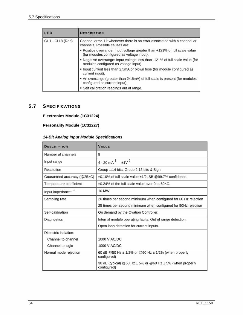
5.7 Specifications
64 REF_1150
LED DE S C RI P T I O N
CH1 - CH 8 (Red) Channel error. Lit whenever there is an error associated with a channel or channels. Possible causes are: Positive overrange: Input voltage greater than +121% of full scale value (for modules configured as voltage input).
Negative overrange: Input voltage less than -121% of full scale value (for modules configured as voltage input).
Input current less than 2.5mA or blown fuse (for module configured as current input).
An overrange (greater than 24.6mA) of full scale is present (for modules configured as current input).
Self calibration readings out of range.
5.7 SPECIFICATIONS
Electronics Module (1C31224)
Personality Module (1C31227)
14-Bit Analog Input Module Specifications
DE S C RI P T I O N VAL U E
Number of channels 8
Input range 4 - 20 mA 1 ±1V 2
Resolution Group 1:14 bits, Group 2:13 bits & Sign
Guaranteed accuracy (@25×C) ±0.10% of full scale value ±1/2LSB @99.7% confidence.
Temperature coefficient ±0.24% of the full scale value over 0 to 60×C.
Input impedance: 3 10 MW
Sampling rate 20 times per second minimum when configured for 60 Hz rejection
25 times per second minimum when configured for 50Hz rejection
Self-calibration On demand by the Ovation Controller.
Diagnostics Internal module operating faults. Out of range detection.
Open loop detection for current inputs.
Dielectric isolation:
Channel to channel
Channel to logic
1000 V AC/DC
1000 V AC/DC
Normal mode rejection 60 dB @50 Hz ± 1/2% or @60 Hz ± 1/2% (when properly configured)
30 dB (typical) @50 Hz ± 5% or @60 Hz ± 5% (when properly configured)
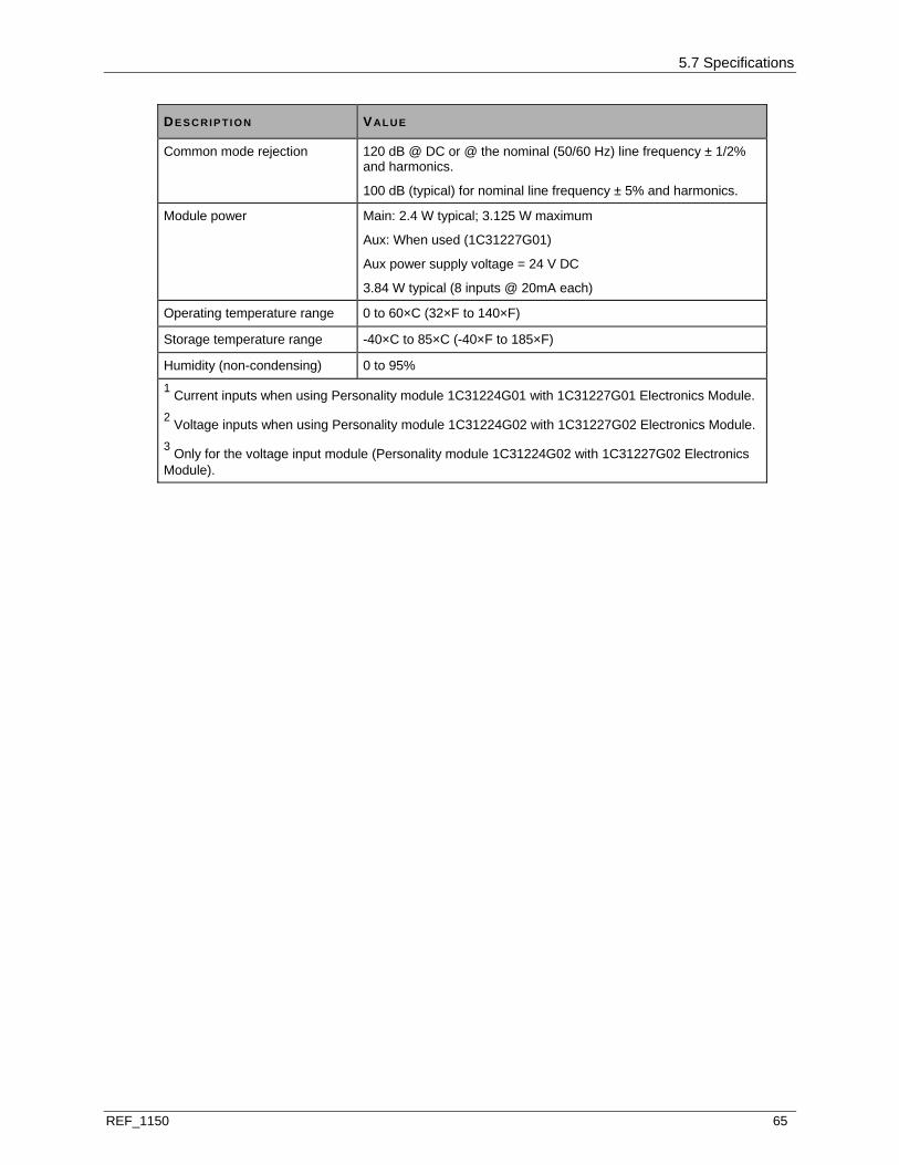
5.7 Specifications
REF_1150 65
DE S C RI P T I O N VAL U E
Common mode rejection 120 dB @ DC or @ the nominal (50/60 Hz) line frequency ± 1/2% and harmonics.
100 dB (typical) for nominal line frequency ± 5% and harmonics.
Module power Main: 2.4 W typical; 3.125 W maximum
Aux: When used (1C31227G01)
Aux power supply voltage = 24 V DC
3.84 W typical (8 inputs @ 20mA each)
Operating temperature range 0 to 60×C (32×F to 140×F)
Storage temperature range -40×C to 85×C (-40×F to 185×F)
Humidity (non-condensing) 0 to 95% 1 Current inputs when using Personality module 1C31224G01 with 1C31227G01 Electronics Module. 2 Voltage inputs when using Personality module 1C31224G02 with 1C31227G02 Electronics Module. 3 Only for the voltage input module (Personality module 1C31224G02 with 1C31227G02 Electronics Module).

REF_1150 67
IN THIS SECTION
Description ........................................................................................................................ 67 Module Group Information ................................................................................................67 Module Specific Information..............................................................................................69 Wiring Information .............................................................................................................74 Address Location Information ...........................................................................................82 Diagnostic LEDs................................................................................................................91 Specifications .................................................................................................................... 92
6.1 DESCRIPTION
The combined Personality and Electronics Modules form the High Speed Analog Input Module. Eight sets of individually isolated input channels provide 14-bit resolution with 50 or 60 samples per second conversion rates. The input signals are conditioned and routed through the appropriate Personality Module to the Electronics Module. The Personality Module also provides surge protection to protect the input circuits of the Electronics Module. The Electronics Module performs the analog to digital conversions and provides interfacing to the Ovation Serial I/O Bus.
The 14 bit High Speed Analog Input is applicable for CE Mark certified systems.
Note: I/O Module General Information (see page 15) contains information on for environmental, installation, wiring, and fuse information for I/O modules.
6.2 MODULE GROUP INFORMATION
6.2.1 ELECTRONICS MODULE (EMOD)
There are four groups of Electronics modules for the High Speed Analog Input Module:
5X00070G01 interfaces to current signals with an input range of 4 to 20 mA. 5X00070G02 interfaces to voltage signals with an input range of ±1V, ±250mV, ±100mV. 5X00070G03 interfaces to voltage signals with an input range of ±5V, ±10V. 5X00070G04 interfaces to thermocouple inputs ± 20mV, ± 50Vm, ± 100mV.
S E C T I O N 6
ANALOG HIGH SPEED INPUT MODULE (14 BITS)
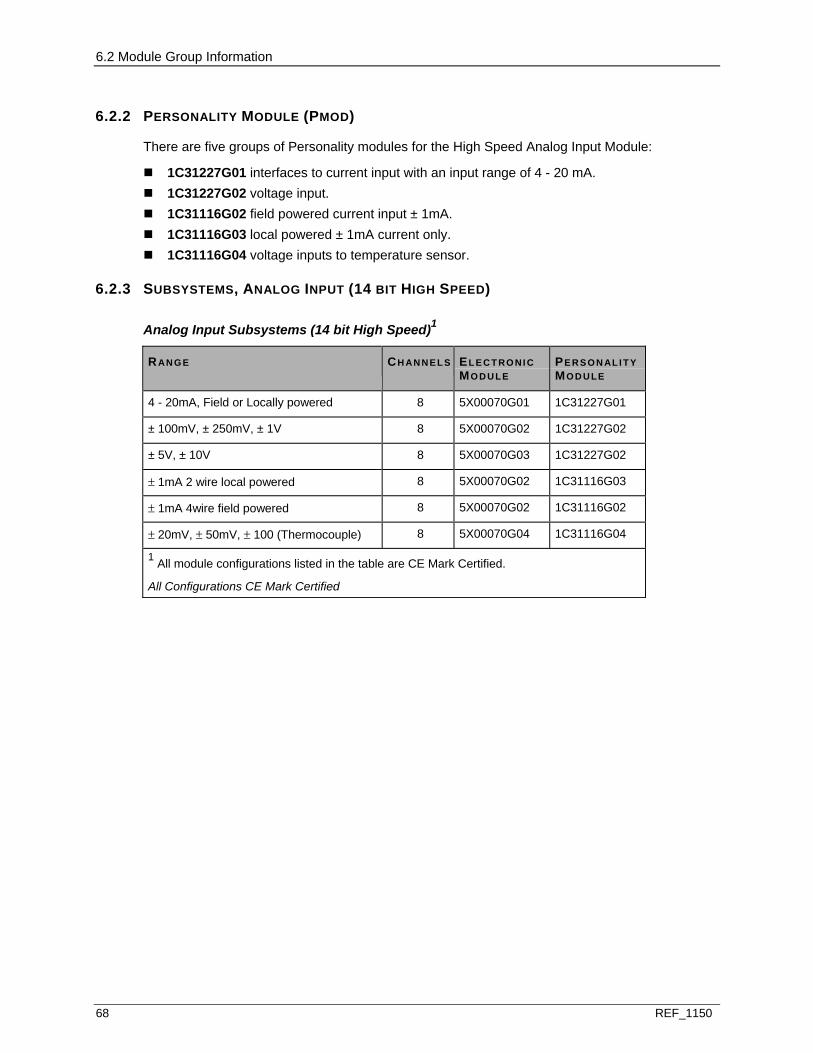
6.2 Module Group Information
68 REF_1150
6.2.2 PERSONALITY MODULE (PMOD)
There are five groups of Personality modules for the High Speed Analog Input Module:
1C31227G01 interfaces to current input with an input range of 4 - 20 mA. 1C31227G02 voltage input. 1C31116G02 field powered current input ± 1mA. 1C31116G03 local powered ± 1mA current only. 1C31116G04 voltage inputs to temperature sensor.
6.2.3 SUBSYSTEMS, ANALOG INPUT (14 BIT HIGH SPEED)
Analog Input Subsystems (14 bit High Speed)1
RAN G E CH AN N E L S EL E C T RO NI C MO D U LE
PE R S O N AL I T Y MO D U LE
4 - 20mA, Field or Locally powered 8 5X00070G01 1C31227G01
± 100mV, ± 250mV, ± 1V 8 5X00070G02 1C31227G02
± 5V, ± 10V 8 5X00070G03 1C31227G02
± 1mA 2 wire local powered 8 5X00070G02 1C31116G03
± 1mA 4wire field powered 8 5X00070G02 1C31116G02
± 20mV, ± 50mV, ± 100 (Thermocouple) 8 5X00070G04 1C31116G04
1 All module configurations listed in the table are CE Mark Certified.
All Configurations CE Mark Certified
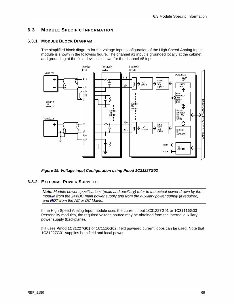
6.3 Module Specific Information
REF_1150 69
6.3 MODULE SPECIFIC INFORMATION
6.3.1 MODULE BLOCK DIAGRAM
The simplified block diagram for the voltage input configuration of the High Speed Analog Input module is shown in the following figure. The channel #1 input is grounded locally at the cabinet, and grounding at the field device is shown for the channel #8 input.
Figure 19: Voltage input Configuration using Pmod 1C31227G02
6.3.2 EXTERNAL POWER SUPPLIES
Note: Module power specifications (main and auxiliary) refer to the actual power drawn by the module from the 24VDC main power supply and from the auxiliary power supply (if required) and NOT from the AC or DC Mains.
If the High Speed Analog Input module uses the current input 1C31227G01 or 1C31116G03 Personality modules, the required voltage source may be obtained from the internal auxiliary power supply (backplane).
If it uses Pmod 1C31227G01 or 1C1116G02, field powered current loops can be used. Note that 1C31227G01 supplies both field and local power.

6.3 Module Specific Information
70 REF_1150
6.3.3 THERMOCOUPLE FUNCTION
When two dissimilar metals (a thermocouple) are joined together, a voltage (the Seebeck Voltage) is generated between them. This voltage is directly related to the temperature at the junction of the two metals. The relationship between the voltage and the temperature can be best described by a fifth order polynomial, determined by the two types of metals that are joined.
To measure the voltage (Vt) between the two metals, a voltmeter (in this case, an analog input card) must be connected to each wire. Unfortunately, this produces two new junctions and voltages (V1 and V2) between the terminals and the thermocouples. The following formula is used to find Vt: Vt = Vm -V1 -V2.
It is not possible to measure V1 and V2 without inducing more junctions and voltages; therefore, the analog input subsystem has a temperature sensor on the Personality module (1C31116G04) to measure the temperature (Tj) at the terminal block of the base unit.
A conversion formula, determined from the junction metal and thermocouple metals, is used to calculate the combined voltage of V1 and V2. This is called Cold Junction Compensation.
Figure 20: Thermocouple Illustration
6.3 Module Specific Information
REF_1150 71
Temperature Sensor Personality Module (1C31116G04)
Personality module 1C1116G04 of the analog input subsystem includes a temperature sensor IC. This is used for measuring the temperature of the terminal block to provide cold junction compensation for thermocouple inputs.
This module is used in conjunction with a terminal block cover (1C31207H01) to maintain a uniform temperature of the terminal block and sensor area. The cover fits over an entire base; however, the sensor only accurately measures the temperature under the half of the cover where the temperature sensor personality module is installed. Therefore, if both modules under the cover require cold junction compensation, they each require the temperature sensor personality module.
Note: Installation instructions for the terminal block cover are provided in the Temperature Compensation Cover Mounting Kit (1B30047G01).
The Group 4 Personality module provides a terminal block temperature measurement feature with the following specifications:
Sampling Rate = 600 msec, maximum, 300 msec, typical Resolution = +/- 0.5×C (+/- 0.9 ×F) Accuracy = +/- 0.5×C over a 0×C to 70×C range
(+/- 0.9 ×F over a 32×F to 158×F range)
(See Ovation Record Type Reference Manual, Ovation Point Builder User Guide, and Ovation Developer Studio User Guide.)
Assigning Thermocouple Coefficients
Use the Instrumentation tab of the Point Builder to select the Field Instrumentation Type (B or TB, E or TE, J or TJ, K or TK, R or TR, S or TS, T or TT). The Ovation system then assigns the default thermocouple coefficients based on the Type selected. Refer to the following table for these coefficient definitions.
If you override the default coefficients by entering new values, the new values remain until you select another thermocouple type. The values then return to the values for the type just selected.
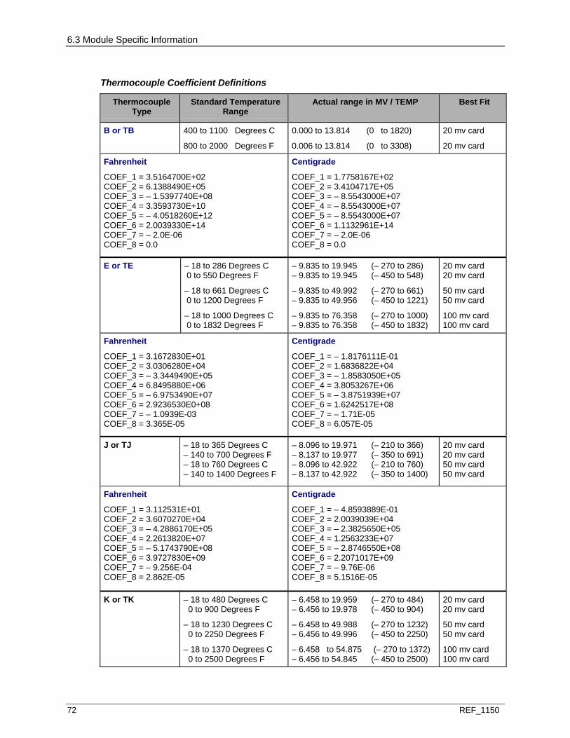
6.3 Module Specific Information
72 REF_1150
Thermocouple Coefficient Definitions
Thermocouple Type
Standard Temperature Range
Actual range in MV / TEMP Best Fit
B or TB 400 to 1100 Degrees C
800 to 2000 Degrees F
0.000 to 13.814 (0 to 1820)
0.006 to 13.814 (0 to 3308)
20 mv card
20 mv card
Fahrenheit
COEF_1 = 3.5164700E+02 COEF_2 = 6.1388490E+05 COEF_3 = – 1.5397740E+08 COEF_4 = 3.3593730E+10 COEF_5 = – 4.0518260E+12 COEF_6 = 2.0039330E+14 COEF_7 = – 2.0E-06 COEF_8 = 0.0
Centigrade
COEF_1 = 1.7758167E+02 COEF_2 = 3.4104717E+05 COEF_3 = – 8.5543000E+07 COEF_4 = – 8.5543000E+07 COEF_5 = – 8.5543000E+07 COEF_6 = 1.1132961E+14 COEF_7 = – 2.0E-06 COEF_8 = 0.0
E or TE – 18 to 286 Degrees C 0 to 550 Degrees F
– 18 to 661 Degrees C 0 to 1200 Degrees F
– 18 to 1000 Degrees C 0 to 1832 Degrees F
– 9.835 to 19.945 (– 270 to 286) – 9.835 to 19.945 (– 450 to 548)
– 9.835 to 49.992 (– 270 to 661) – 9.835 to 49.956 (– 450 to 1221)
– 9.835 to 76.358 (– 270 to 1000) – 9.835 to 76.358 (– 450 to 1832)
20 mv card 20 mv card
50 mv card 50 mv card
100 mv card 100 mv card
Fahrenheit
COEF_1 = 3.1672830E+01 COEF_2 = 3.0306280E+04 COEF_3 = – 3.3449490E+05 COEF_4 = 6.8495880E+06 COEF_5 = – 6.9753490E+07 COEF_6 = 2.9236530E0+08 COEF_7 = – 1.0939E-03 COEF_8 = 3.365E-05
Centigrade
COEF_1 = – 1.8176111E-01 COEF_2 = 1.6836822E+04 COEF_3 = – 1.8583050E+05 COEF_4 = 3.8053267E+06 COEF_5 = – 3.8751939E+07 COEF_6 = 1.6242517E+08 COEF_7 = – 1.71E-05 COEF_8 = 6.057E-05
J or TJ – 18 to 365 Degrees C – 140 to 700 Degrees F – 18 to 760 Degrees C – 140 to 1400 Degrees F
– 8.096 to 19.971 (– 210 to 366) – 8.137 to 19.977 (– 350 to 691) – 8.096 to 42.922 (– 210 to 760) – 8.137 to 42.922 (– 350 to 1400)
20 mv card 20 mv card 50 mv card 50 mv card
Fahrenheit
COEF_1 = 3.112531E+01 COEF_2 = 3.6070270E+04 COEF_3 = – 4.2886170E+05 COEF_4 = 2.2613820E+07 COEF_5 = – 5.1743790E+08 COEF_6 = 3.9727830E+09 COEF_7 = – 9.256E-04 COEF_8 = 2.862E-05
Centigrade
COEF_1 = – 4.8593889E-01 COEF_2 = 2.0039039E+04 COEF_3 = – 2.3825650E+05 COEF_4 = 1.2563233E+07 COEF_5 = – 2.8746550E+08 COEF_6 = 2.2071017E+09 COEF_7 = – 9.76E-06 COEF_8 = 5.1516E-05
K or TK – 18 to 480 Degrees C 0 to 900 Degrees F
– 18 to 1230 Degrees C 0 to 2250 Degrees F
– 18 to 1370 Degrees C 0 to 2500 Degrees F
– 6.458 to 19.959 (– 270 to 484) – 6.456 to 19.978 (– 450 to 904)
– 6.458 to 49.988 (– 270 to 1232) – 6.456 to 49.996 (– 450 to 2250)
– 6.458 to 54.875 (– 270 to 1372) – 6.456 to 54.845 (– 450 to 2500)
20 mv card 20 mv card
50 mv card 50 mv card
100 mv card 100 mv card
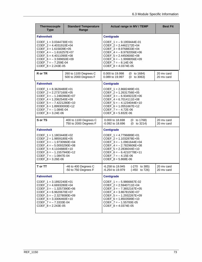
6.3 Module Specific Information
REF_1150 73
Thermocouple Type
Standard Temperature Range
Actual range in MV / TEMP Best Fit
Fahrenheit
COEF_1 = 3.0344730E+01 COEF_2 = 4.4031910E+04 COEF_3 = 1.615839E+05 COEF_4 = – 1.616257E+07 COEF_5 = 4.4011090E+08 COEF_6 = – 3.599650E+09 COEF_7 = – 7.259E-04 COEF_8 = 2.243E-05
Centigrade
COEF_1 = – 9.1959444E-01 COEF_2 = 2.4462172E+04 COEF_3 = 8.9768833E+04 COEF_4 = – 8.9792056E+06 COEF_5 = 2.4450606E+08 COEF_6 = – 1.9998056E+09 COEF_7 = – 8.14E-06 COEF_8 = 4.0374E-05
R or TR 260 to 1100 Degrees C 500 to 2000 Degrees F
0.000 to 19.998 (0 to 1684) 0.089 to 19.997 (0 to 3063)
20 mv card 20 mv card
Fahrenheit
COEF_1 = 8.3628480E+01 COEF_2 = 2.2737160E+05 COEF_3 = – 1.2482860E+07 COEF_4 = 1.2062540E+09 COEF_5 = – 7.4221280E+10 COEF_6 = 1.89930000E+12 COEF_7 = – 1.084E-04 COEF_8 = 3.24E-06
Centigrade
COEF_1 = 2.8682489E+01 COEF_2 = 1.2631756E+05 COEF_3 = – 6.9349222E+06 COEF_4 = 6.7014111E+08 COEF_5 = – 4.1234044E+10 COEF_6 = 1.0551667E+12 COEF_7 = – 4.72E-06 COEF_8 = 5.832E-06
S or TS 400 to 1100 Degrees C 750 to 2000 Degrees F
0.000 to 18.698 (0 to 1768) -0.092 to 18.696 (0 to 3214)
20 mv card 20 mv card
Fahrenheit
COEF_1 = 1.1803440E+02 COEF_2 = 1.9859180E+05 COEF_3 = – 1.9730960E+04 COEF_4 = – 5.0093290E+08 COEF_5 = 4.1104880E+10 COEF_6 = – 1.1557940E+12 COEF_7 = – 1.0847E-04 COEF_8 = 3.26E-06
Centigrade
COEF_1 = 4.7796889E+01 COEF_2 = 1.1032878E+05 COEF_3 = – 1.0961644E+04 COEF_4 = – 2.7829606E+08 COEF_5 = 2.2836044E+10 COEF_6 = – 6.4210778E+11 COEF_7 = – 4.15E-06 COEF_8 = 5.868E-06
T or TT -46 to 400 Degrees C -50 to 750 Degrees F
-6.258 to 19.945 (-270 to 385) -6.254 to 19.979 (-450 to 726)
20 mv card 20 mv card
Fahrenheit
COEF_1 = 3.1892240E+01 COEF_2 = 4.6693280E+04 COEF_3 = – 1.3257390E+06 COEF_4 = 6.9620670E+07 COEF_5 = – 2.3278080E+09 COEF_6 = 3.3306460E+10 COEF_7 = – 7.3333E-04 COEF_8 = 2.243E-05
Centigrade
COEF_1 = – 5.9866667E-02 COEF_2 = 2.5940711E+04 COEF_3 = – 7.3652167E+05 COEF_4 = 3.8678150E+07 COEF_5 = – 1.2932267E+09 COEF_6 = 1.8503589E+10 COEF_7 = – 1.55700E-05 COEF_8 = 4.0374E-05
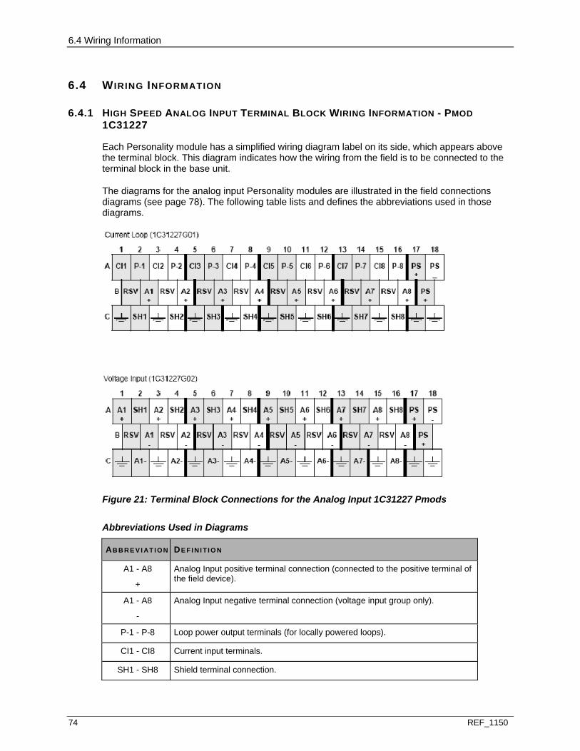
6.4 Wiring Information
74 REF_1150
6.4 WIRING INFORMATION
6.4.1 HIGH SPEED ANALOG INPUT TERMINAL BLOCK WIRING INFORMATION - PMOD 1C31227
Each Personality module has a simplified wiring diagram label on its side, which appears above the terminal block. This diagram indicates how the wiring from the field is to be connected to the terminal block in the base unit.
The diagrams for the analog input Personality modules are illustrated in the field connections diagrams (see page 78). The following table lists and defines the abbreviations used in those diagrams.
Figure 21: Terminal Block Connections for the Analog Input 1C31227 Pmods
Abbreviations Used in Diagrams
AB B R E V I AT I ON DE FI N I T I O N
A1 - A8
+
Analog Input positive terminal connection (connected to the positive terminal of the field device).
A1 - A8
-
Analog Input negative terminal connection (voltage input group only).
P-1 - P-8 Loop power output terminals (for locally powered loops).
CI1 - CI8 Current input terminals.
SH1 - SH8 Shield terminal connection.

6.4 Wiring Information
REF_1150 75
AB B R E V I AT I ON DE FI N I T I O N
RSV Reserved terminal. No connections allowed on these terminals.
Earth ground terminals.
PS+, PS- Auxiliary power supply terminals.
Use shielded twisted pair wire for the field wiring. Tie the Analog Input negative terminal and shield together and to earth ground, either locally at the cabinet or at the field device. Voltage inputs use the 1C31227G02 Personality Modules. Grounding the shield and the analog input negative terminal at the cabinet or at the field device is arranged by the proper Terminal Block connections.
Similarly, current inputs using the 1C31227G01 Personality Modules can accommodate field or locally powered devices by using the correct terminal block connections.
The Personality Modules have a field connection diagram label on top of each module to facilitate field wiring. The following figures show the implementations of the field connections for the various Personality Module and field device combinations.
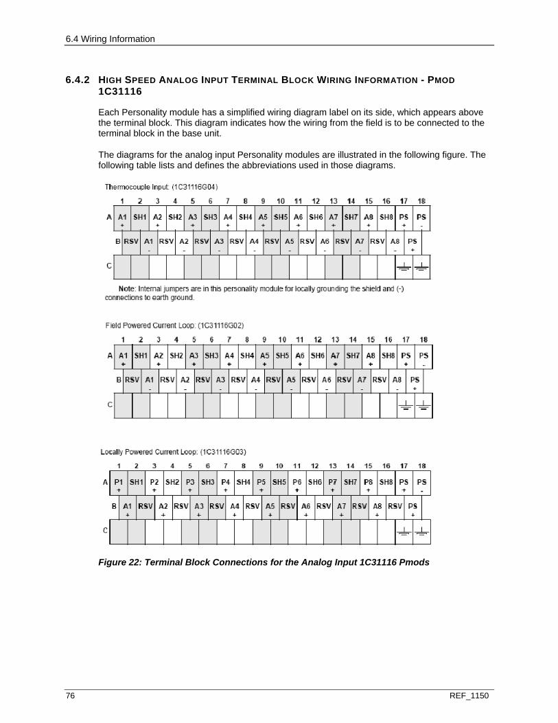
6.4 Wiring Information
76 REF_1150
6.4.2 HIGH SPEED ANALOG INPUT TERMINAL BLOCK WIRING INFORMATION - PMOD 1C31116
Each Personality module has a simplified wiring diagram label on its side, which appears above the terminal block. This diagram indicates how the wiring from the field is to be connected to the terminal block in the base unit.
The diagrams for the analog input Personality modules are illustrated in the following figure. The following table lists and defines the abbreviations used in those diagrams.
Figure 22: Terminal Block Connections for the Analog Input 1C31116 Pmods
6.4 Wiring Information
REF_1150 77
Terminal Block Connections for the Analog Input 1C31116 Pmods
Abbreviations Used in Diagrams
AB B R E V I AT I ON DE FI N I T I O N
A1 - A8
+
Analog Input positive terminal connection.
A1 - A8
-
Analog Input negative terminal connection.
Earth ground terminals.
P1 - P8
+
Positive terminal connection for current loop power.
PS+, PS- Auxiliary power supply terminals.
RSV Reserved terminal. No connections allowed on these terminals.
SH1 - SH8 Shield terminal connection (for non-CE Mark certified systems).
Note: Do not use unmarked terminal block locations.
Shield terminals (SH) are not connected in CE Mark systems.
6.4.3 HIGH SPEED ANALOG INPUT FIELD CONNECTION WIRING DIAGRAMS
As is standard for analog signals, shielded twisted-pair wire should be used for the field interface. For the analog input, the negative (-) and shield should be tied together and to earth ground, either locally at the cabinet or at the field device.
The following four figures show how the various Personality modules require these connections or how the options are implemented. The fifth drawing illustrates the jumper settings for the Personality module.

6.4 Wiring Information
78 REF_1150
6.4.4 NON-CE MARK SYSTEMS
Figure 23: Field Connections for the Input Connectors (Non-CE Mark)

6.4 Wiring Information
REF_1150 79
6.4.5 CE MARK SYSTEMS
Figure 24: Field Connections for the Input Connectors (CE Mark)

6.4 Wiring Information
80 REF_1150
6.4.6 NON-CE MARK CERTIFIED SYSTEMS
Figure 25: Field Connections for the Analog Input Pmod (Non-CE Mark)
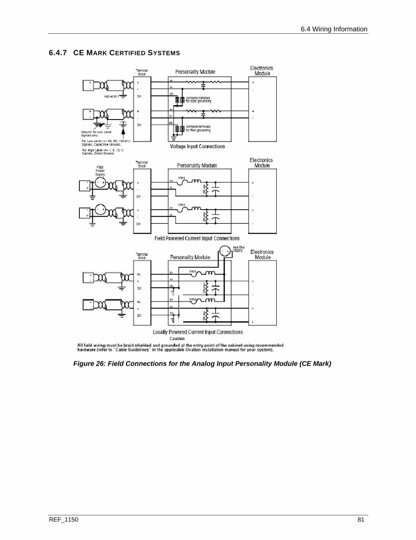
6.4 Wiring Information
REF_1150 81
6.4.7 CE MARK CERTIFIED SYSTEMS
Figure 26: Field Connections for the Analog Input Personality Module (CE Mark)
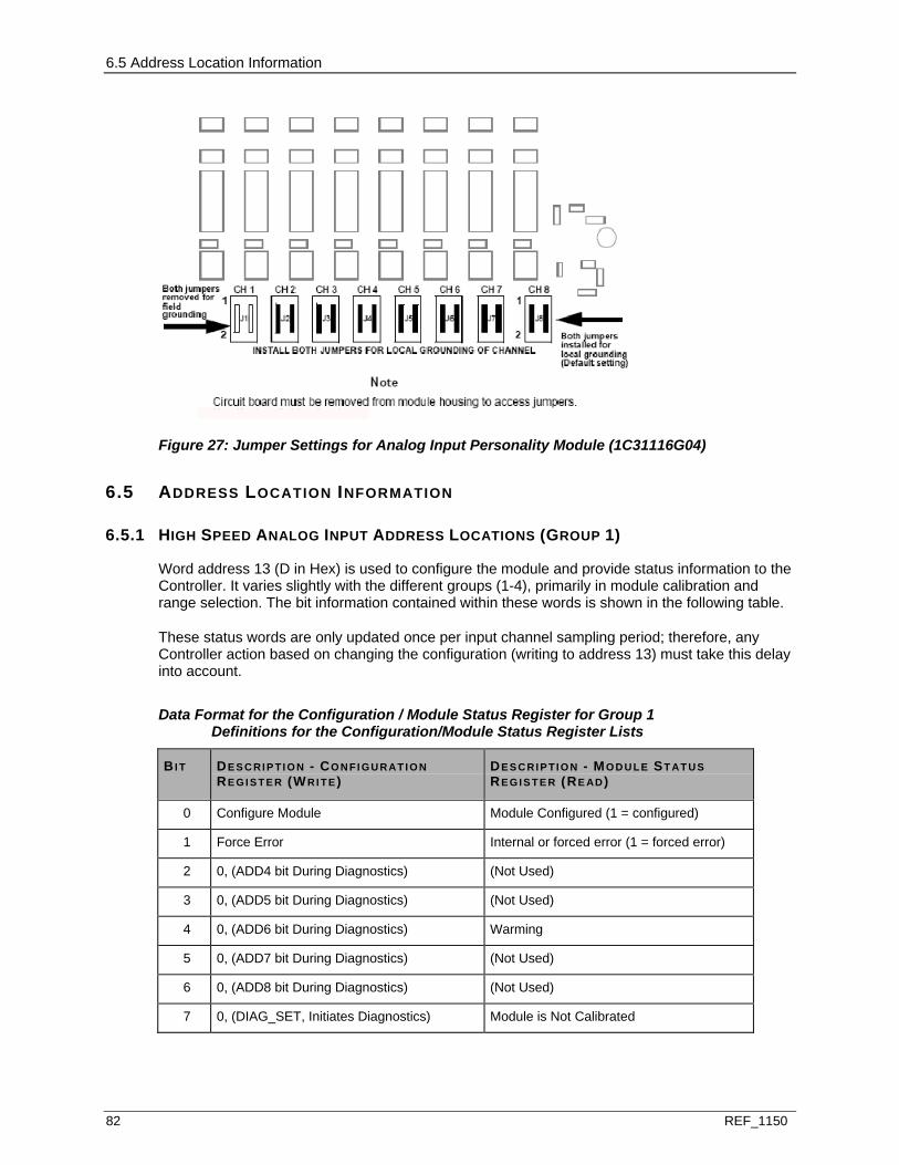
6.5 Address Location Information
82 REF_1150
Figure 27: Jumper Settings for Analog Input Personality Module (1C31116G04)
6.5 ADDRESS LOCATION INFORMATION
6.5.1 HIGH SPEED ANALOG INPUT ADDRESS LOCATIONS (GROUP 1)
Word address 13 (D in Hex) is used to configure the module and provide status information to the Controller. It varies slightly with the different groups (1-4), primarily in module calibration and range selection. The bit information contained within these words is shown in the following table.
These status words are only updated once per input channel sampling period; therefore, any Controller action based on changing the configuration (writing to address 13) must take this delay into account.
Data Format for the Configuration / Module Status Register for Group 1 Definitions for the Configuration/Module Status Register Lists
BI T DE S C RI P T I O N - CO N FI GU RAT I O N RE GI S T E R (WRI T E)
DE S C RI P T I O N - MO D U LE ST AT U S RE GI S T E R (RE AD)
0 Configure Module Module Configured (1 = configured)
1 Force Error Internal or forced error (1 = forced error)
2 0, (ADD4 bit During Diagnostics) (Not Used)
3 0, (ADD5 bit During Diagnostics) (Not Used)
4 0, (ADD6 bit During Diagnostics) Warming
5 0, (ADD7 bit During Diagnostics) (Not Used)
6 0, (ADD8 bit During Diagnostics) (Not Used)
7 0, (DIAG_SET, Initiates Diagnostics) Module is Not Calibrated

6.5 Address Location Information
REF_1150 83
8 50/60 Hz Selection (1 = 50Hz) 50 Hz/60 Hz System (1 = 50Hz)
9 Not Defined (Not Used)
10 0, (Initiates system calibration during Diagnostics)
SYS_CAL In Progress (During Diagnostics)
11 SELF_CAL (Initiates Self Calibration) SYS_CAL Completed (During Diagnostics)
12 Not Defined SYS_CAL Failed (During Diagnostics)
13 Not Defined Internal Memory Error
14 Not Defined Module In Diagnostic Mode (During Diagnostics)
15 Not Defined Point Fault 1
1 Refer to the Point Quality Register for the descriptions of the Point Faults.
Bits defined for Diagnostics are only used during factory testing.
The bit definitions for this register are encoded as shown in the above table and described below:
Bit 0: This bit configures the module (write) or indicates the configuration state of the module (read). A “1” indicates that the module is configured. Note that until the module is configured, reading from addresses 0 through 11 (B in Hex) produces an attention status.
Bit 1: This bit (write “1”) forces the module into the error state, resulting in the error LED being lit. The read of bit “1” indicates that there is an internal module error, or the Controller has forced the module into the error state. The state of this bit is always reflected by the module’s Internal Error LED. Whenever this bit is set, an attention status is returned to the Controller when addresses 0 through 11 (B in Hex) are read.
Bits 2-3: These bits are not used and are read as “0” under normal operation.
Bit 4: This bit (read) indicates that the module is in the Warming state. This state exists after power up and terminates after 8.16 seconds. The module is in the error condition during the warm up period.
Bits 5-6: These bits are not used and read as “0” under normal operation.
Bit 7: This bit (read) is the result of a checksum test of the EEPROM. A failure of this test can indicate a bad EEPROM, but it typically indicates that the module has not been calibrated. A “0” indicates that there is no error condition. If an error is present, the module error LED is lit. The point fault bit is also set since all the point data is not calibrated. The “1” state of this bit indicates an unrecoverable error condition in the field.
Bit 8: The status of this bit (read) indicates the conversion rate of the module; write to this bit configures the conversion rate of A/D converters as shown in the following table.
Conversion Rate (1/sec.) Bit 8
60 (for 60Hz systems) 0
50 (for 50Hz systems) 1
Bit 9: This bit is not used and is read as “0” under normal operation.
Bit 10: This bit is not used and is read as “0” under normal operation.
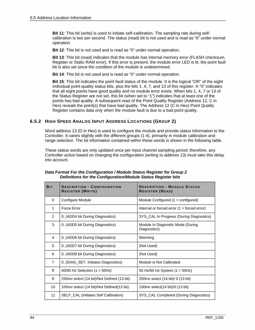
6.5 Address Location Information
84 REF_1150
Bit 11: This bit (write) is used to initiate self-calibration. The sampling rate during self-calibration is two per second. The status (read) bit is not used and is read as “0” under normal operation
Bit 12: This bit is not used and is read as “0” under normal operation.
Bit 13: This bit (read) indicates that the module has internal memory error (FLASH checksum, Register or Static RAM error). If this error is present, the module error LED is lit, the point fault bit is also set since the condition of the module is undetermined.
Bit 14: This bit is not used and is read as “0” under normal operation.
Bit 15: This bit indicates the point fault status of the module. It is the logical “OR” of the eight individual point-quality status bits, plus the bits 1, 4, 7, and 13 of this register. A “0” indicates that all eight points have good quality and no module error exists. When bits 1, 4, 7 or 13 of the Status Register are not set, this bit (when set to “1”) indicates that at least one of the points has bad quality. A subsequent read of the Point Quality Register (Address 12, C in Hex) reveals the point(s) that have bad quality. The Address 12 (C in Hex) Point Quality Register contains data only when the module fault is due to a bad point quality.
6.5.2 HIGH SPEED ANALOG INPUT ADDRESS LOCATIONS (GROUP 2)
Word address 13 (D in Hex) is used to configure the module and provide status information to the Controller. It varies slightly with the different groups (1-4), primarily in module calibration and range selection. The bit information contained within these words is shown in the following table.
These status words are only updated once per input channel sampling period; therefore, any Controller action based on changing the configuration (writing to address 13) must take this delay into account.
Data Format For the Configuration / Module Status Register for Group 2 Definitions for the Configuration/Module Status Register bits
BI T DE S C RI P T I O N - CO N FI GU RAT I O N RE GI S T E R (WRI T E)
DE S C RI P T I O N - MO D U LE ST AT U S RE GI S T E R (RE AD)
0 Configure Module Module Configured (1 = configured)
1 Force Error Internal or forced error (1 = forced error)
2 0, (ADD4 bit During Diagnostics) SYS_CAL In Progress (During Diagnostics)
3 0, (ADD5 bit During Diagnostics) Module In Diagnostic Mode (During Diagnostics)
4 0, (ADD6 bit During Diagnostics) Warming
5 0, (ADD7 bit During Diagnostics) (Not Used)
6 0, (ADD8 bit During Diagnostics) (Not Used)
7 0, (DIAG_SET, Initiates Diagnostics) Module is Not Calibrated
8 50/60 Hz Selection (1 = 50Hz) 50 Hz/60 Hz System (1 = 50Hz)
9 250mv select (14 bit)/Not Defined (13 bit) 250mv select (14 bit)/ 0 (13 bit)
10 100mv select (14 bit)/Not Defined(13 bit) 100mv select(14 bit)/0 (13 bit)
11 SELF_CAL (Initiates Self Calibration) SYS_CAL Completed (During Diagnostics)

6.5 Address Location Information
REF_1150 85
12 0, (Initiates system calibration during Diagnostics)
SYS_CAL Failed (During Diagnostics)
13 0, Lock Calibration Gain (concurrent with the initiation of calibration during diagnostics)
Internal Memory Error
14 0, Clear Calibration (concurrent with the initiation of calibration during diagnostics)
(Not Used)1
15 Not Defined Point Fault 1
1 Refer to the Point Quality Register for the descriptions of the Point Faults
Bits defined for Diagnostics are only used during factory testing.
The bit definitions for this register are encoded as shown in the above table and described below:
Bit 0: This bit configures the module (write) or indicates the configuration state of the module (read). A “1” indicates that the module is configured. Note that until the module is configured, reading from addresses 0 through 11 (B in Hex) produces an attention status.
Bit 1: This bit (write “1”) forces the module into the error state, resulting in the error LED being lit. The read of bit “1” indicates that there is an internal module error, or the Controller has forced the module into the error state. The state of this bit is always reflected by the module’s Internal Error LED. Whenever this bit is set, an attention status is returned to the Controller when addresses 0 through 11 (B in Hex) are read.
Bits 2-3: These bits are not used and are read as “0” under normal operation.
Bit 4: This bit (read) indicates that the module is in the Warming state. This state exists after power up and terminates after 8.16 seconds. The module is in the error condition during the warm up period.
Bits 5-6: These bits are not used and are read as “0” under normal operation.
Bit 7: This bit (read) is the result of a checksum test of the EEPROM. A failure of this test can indicate a bad EEPROM, but it typically indicates that the module has not been calibrated. A “0” indicates that there is no error condition. If an error is present, the module error LED is lit. The point fault bit is also set since all the point data is not calibrated. The “1” state of this bit indicates an unrecoverable error condition in the field.
Bit 8: The status of this bit (read) indicates the conversion rate of the module, write to this bit configures the conversion rate of A/D converters as shown in the following table.
Conversion Rate (1/sec.) Bit 8
60 (for 60Hz systems) 0
50 (for 50Hz systems) 1
Bits 9-10: These bits are used to configure the ranges.
Full Scale Bit 9 Bit 10
1V 0 0
250 mv 1 0
100 mv 0 1
invalid 1 1
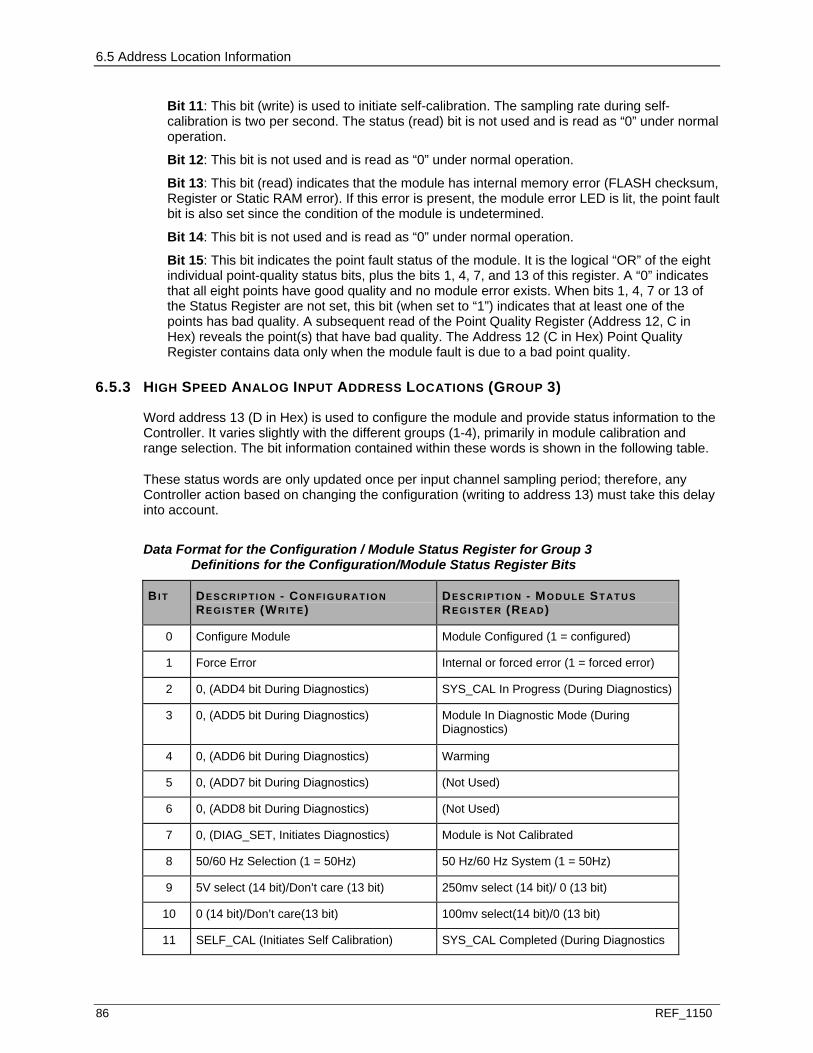
6.5 Address Location Information
86 REF_1150
Bit 11: This bit (write) is used to initiate self-calibration. The sampling rate during self-calibration is two per second. The status (read) bit is not used and is read as “0” under normal operation.
Bit 12: This bit is not used and is read as “0” under normal operation.
Bit 13: This bit (read) indicates that the module has internal memory error (FLASH checksum, Register or Static RAM error). If this error is present, the module error LED is lit, the point fault bit is also set since the condition of the module is undetermined.
Bit 14: This bit is not used and is read as “0” under normal operation.
Bit 15: This bit indicates the point fault status of the module. It is the logical “OR” of the eight individual point-quality status bits, plus the bits 1, 4, 7, and 13 of this register. A “0” indicates that all eight points have good quality and no module error exists. When bits 1, 4, 7 or 13 of the Status Register are not set, this bit (when set to “1”) indicates that at least one of the points has bad quality. A subsequent read of the Point Quality Register (Address 12, C in Hex) reveals the point(s) that have bad quality. The Address 12 (C in Hex) Point Quality Register contains data only when the module fault is due to a bad point quality.
6.5.3 HIGH SPEED ANALOG INPUT ADDRESS LOCATIONS (GROUP 3)
Word address 13 (D in Hex) is used to configure the module and provide status information to the Controller. It varies slightly with the different groups (1-4), primarily in module calibration and range selection. The bit information contained within these words is shown in the following table.
These status words are only updated once per input channel sampling period; therefore, any Controller action based on changing the configuration (writing to address 13) must take this delay into account.
Data Format for the Configuration / Module Status Register for Group 3 Definitions for the Configuration/Module Status Register Bits
BI T DE S C RI P T I O N - CO N FI GU RAT I O N RE GI S T E R (WRI T E)
DE S C RI P T I O N - MO D U LE ST AT U S RE GI S T E R (RE AD)
0 Configure Module Module Configured (1 = configured)
1 Force Error Internal or forced error (1 = forced error)
2 0, (ADD4 bit During Diagnostics) SYS_CAL In Progress (During Diagnostics)
3 0, (ADD5 bit During Diagnostics) Module In Diagnostic Mode (During Diagnostics)
4 0, (ADD6 bit During Diagnostics) Warming
5 0, (ADD7 bit During Diagnostics) (Not Used)
6 0, (ADD8 bit During Diagnostics) (Not Used)
7 0, (DIAG_SET, Initiates Diagnostics) Module is Not Calibrated
8 50/60 Hz Selection (1 = 50Hz) 50 Hz/60 Hz System (1 = 50Hz)
9 5V select (14 bit)/Don’t care (13 bit) 250mv select (14 bit)/ 0 (13 bit)
10 0 (14 bit)/Don’t care(13 bit) 100mv select(14 bit)/0 (13 bit)
11 SELF_CAL (Initiates Self Calibration) SYS_CAL Completed (During Diagnostics

6.5 Address Location Information
REF_1150 87
12 0, (Initiates system calibration during Diagnostics)
SYS_CAL Failed (During Diagnostics)
13 0, Lock Calibration Gain (concurrent with the initiation of calibration during diagnostics)
Internal Memory Error
14 0, Clear Calibration (concurrent with the initiation of calibration during diagnostics)
(Not Used)
15 Not Defined Point Fault 1
1 Refer to the Point Quality Register for the descriptions of the Point Faults.
Bits defined for Diagnostics are only used during factory testing.
The bit definitions for this register are encoded as shown in the above table and described below:
Bit 0: This bit configures the module (write) or indicates the configuration state of the module (read). A “1” indicates that the module is configured. Note that until the module is configured, reading from addresses 0 through 11 (B in Hex) produces an attention status.
Bit 1: This bit (write “1”) forces the module into the error state, resulting in the error LED being lit. The read of bit “1” indicates that there is an internal module error, or the Controller has forced the module into the error state. The state of this bit is always reflected by the module’s Internal Error LED. Whenever this bit is set, an attention status is returned to the Controller when addresses 0 through 11 (B in Hex) are read.
Bits 2-3: These bits are not used and are read as “0” under normal operation.
Bit 4: This bit (read) indicates that the module is in the Warming state. This state exists after power up and terminates after 8.16 seconds. The module is in the error condition during the warm up period.
Bits 5-6: These bits are not used and are read as “0” under normal operation.
Bit 7: This bit (read) is the result of a checksum test of the EEPROM. A failure of this test can indicate a bad EEPROM, but it typically indicates that the module has not been calibrated. A “0” indicates that there is no error condition. If an error is present, the module error LED is lit. The point fault bit is also set since all the point data is not calibrated. The “1” state of this bit indicates an unrecoverable error condition in the field.
Bit 8: The status of this bit (read) indicates the conversion rate of the module, write to this bit configures the conversion rate of A/D converters as shown in the following table.
Conversion Rate (1/sec.) Bit 8
60 (for 60Hz systems) 0
50 (for 50Hz systems) 1
Bits 9-10: These bits are used to configure the ranges as follows for 14 bit operation. For 13 bit operation, these bits have no meaning.
Full Scale Bit 9 Bit 10
10V 0 0
5V 1 0
2.5V(not supported) 0 1

6.5 Address Location Information
88 REF_1150
invalid 1 1
Bit 11: This bit (write) is used to initiate self-calibration. The sampling rate during self-calibration is two per second. The status (read) bit is not used and read as “0” under normal operation.
Bit 12: This bit is not used and is read as “0” under normal operation.
Bit 13: This bit (read) indicates that the module has internal memory error (FLASH checksum, Register or Static RAM error). If this error is present, the module error LED is lit, the point fault bit is also set as the condition of the module is undetermined.
Bit 14: This bit is not used and is read as “0” under normal operation.
Bit 15: This bit indicates the point fault status of the module. It is the logical “OR” of the eight individual point-quality status bits, plus the bits 1, 4, 7, and 13 of this register. A “0” indicates that all eight points have good quality and no module error exists. When bits 1, 4, 7 or 13 of the Status Register are not set, this bit (when set to “1”) indicates that at least one of the points has bad quality. A subsequent read of the Point Quality Register (Address 12, C in Hex) reveals the point(s) that have bad quality. The Address 12 (C in Hex) Point Quality Register contains data only when the module fault is due to a bad point quality.
6.5.4 HIGH SPEED ANALOG INPUT ADDRESS LOCATIONS (GROUP 4)
Word address 13 (D in Hex) is used to configure the module and provide status information to the Controller. It varies slightly with the different groups (1-4), primarily in module calibration and range selection. The bit information contained within these words is shown in the following tables.
These status words are only updated once per input channel sampling period; therefore, any Controller action based on changing the configuration (writing to address 13) must take this delay into account.
Data Format for the Configuration / Module Status Register for Group 4 Definitions for the Configuration/Module Status Register Bits
BI T DE S C RI P T I O N - CO N FI GU RAT I O N RE GI S T E R (WRI T E)
DE S C RI P T I O N - MO D U LE ST AT U S RE GI S T E R (RE AD)
0 Configure Module Module Configured (1 = configured)
1 Force Error Internal or forced error (1 = forced error)
2 0, (ADD4 bit During Diagnostics) SYS_CAL In Progress (During Diagnostics)
3 0, (ADD5 bit During Diagnostics) Module In Diagnostic Mode (During Diagnostics)
4 0, (ADD6 bit During Diagnostics) Warming
5 0, (ADD7 bit During Diagnostics) (Not Used)
6 0, (ADD8 bit During Diagnostics) (Not Used)
7 0, (DIAG_SET, Initiates Diagnostics) Module is Not Calibrated
8 50/60 Hz Selection (1 = 50Hz) 50 Hz/60 Hz System (1 = 50Hz)
9 50mv select (14 bit)/Don’t care (13 bit) 50mv select (14 bit)/ 0 (13 bit)
10 100mv select (14 bit)/Don’t care(13 bit) 100mv select (14 bit)/0 (13 bit)

6.5 Address Location Information
REF_1150 89
11 SELF_CAL (Initiates Self Calibration) SYS_CAL Completed (During Diagnostics)
12 0, (Initiates system calibration during Diagnostics)
SYS_CAL Failed (During Diagnostics)
13 0, Lock Calibration Gain (concurrent with the initiation of calibration during diagnostics)
Internal Memory Error
14 0, Clear Calibration (concurrent with the initiation of calibration during diagnostics)
Temperature Sensor Failure
15 Not Defined Point Fault 1
1 Refer to the Point Quality Register for the descriptions of the Point Faults
Bits defined for Diagnostics are only used during factory testing.
The bit definitions for this register are encoded as shown in the above table and described below:
Bit 0: This bit configures the module (write) or indicates the configuration state of the module (read). A “1” indicates that the module is configured. Note that until the module is configured, reading from addresses 0 through 11 (B in Hex) will produce an attention status.
Bit 1: This bit (write “1”) forces the module into the error state, resulting in the error LED being lit. The read of bit “1” indicates that there is an internal module error, or the Controller has forced the module into the error state. The state of this bit is always reflected by the module’s Internal Error LED. Whenever this bit is set, an attention status is returned to the Controller when addresses 0 through 11 (B in Hex) are read.
Bits 2-3: These bits are not used and are read as “0” under normal operation.
Bit 4: This bit (read) indicates that the module is in the “Warming” state. This state exists after power up and terminates after 8.16 seconds. The module will be in the error condition during the warm up period.
Bits 5-6: These bits are not used and are read as “0” under normal operation.
Bit 7: This bit (read) is the result of a checksum test of the EEPROM. A failure of this test can indicate a bad EEPROM, but it typically indicates that the module has not been calibrated. A “0” indicates that there is no error condition. If an error is present, the module error LED is lit. The point fault bit will also be set as all the point data is not calibrated. The “1” state of this bit indicates an unrecoverable error condition in the field.
Bit 8: The status of this bit (read) indicates the conversion rate of the input module, write to this bit configures the conversion rate of A/D converters as shown in the following table.
Conversion Rate (1/sec.) Bit 8
60 (for 60Hz systems) 0
50 (for 50Hz systems) 1
Bits 9-10: These bits are used to configure the ranges as follows
Full Scale Bit 9 Bit 10
20 mv 0 0
50 mv 1 0
100 mv 0 1
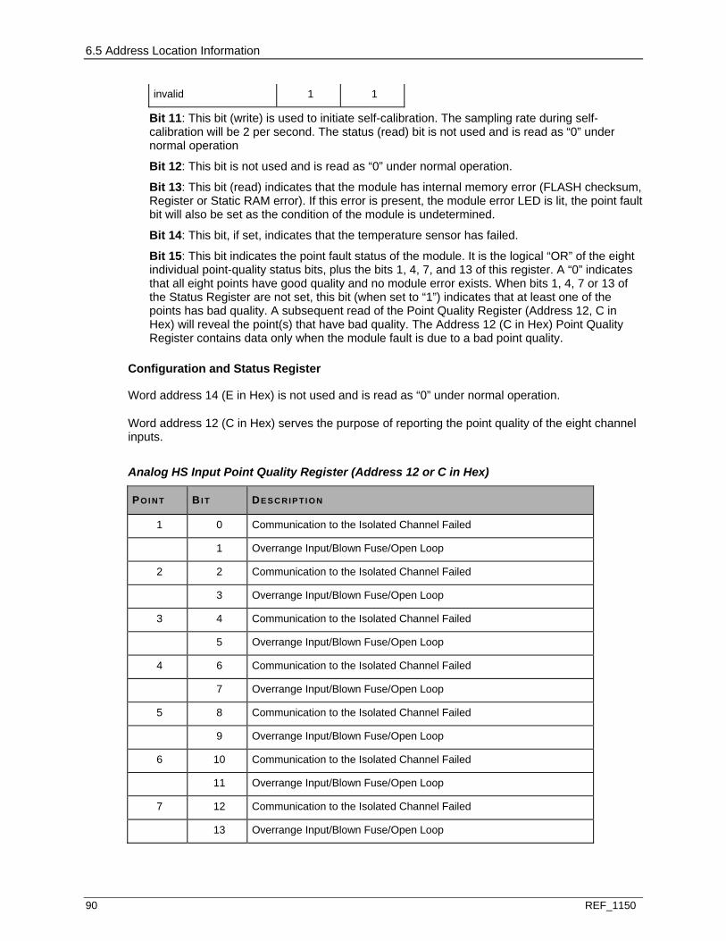
6.5 Address Location Information
90 REF_1150
invalid 1 1
Bit 11: This bit (write) is used to initiate self-calibration. The sampling rate during self-calibration will be 2 per second. The status (read) bit is not used and is read as “0” under normal operation
Bit 12: This bit is not used and is read as “0” under normal operation.
Bit 13: This bit (read) indicates that the module has internal memory error (FLASH checksum, Register or Static RAM error). If this error is present, the module error LED is lit, the point fault bit will also be set as the condition of the module is undetermined.
Bit 14: This bit, if set, indicates that the temperature sensor has failed.
Bit 15: This bit indicates the point fault status of the module. It is the logical “OR” of the eight individual point-quality status bits, plus the bits 1, 4, 7, and 13 of this register. A “0” indicates that all eight points have good quality and no module error exists. When bits 1, 4, 7 or 13 of the Status Register are not set, this bit (when set to “1”) indicates that at least one of the points has bad quality. A subsequent read of the Point Quality Register (Address 12, C in Hex) will reveal the point(s) that have bad quality. The Address 12 (C in Hex) Point Quality Register contains data only when the module fault is due to a bad point quality.
Configuration and Status Register
Word address 14 (E in Hex) is not used and is read as “0” under normal operation.
Word address 12 (C in Hex) serves the purpose of reporting the point quality of the eight channel inputs.
Analog HS Input Point Quality Register (Address 12 or C in Hex)
POI NT BI T DE S C RI P T I O N
1 0 Communication to the Isolated Channel Failed
1 Overrange Input/Blown Fuse/Open Loop
2 2 Communication to the Isolated Channel Failed
3 Overrange Input/Blown Fuse/Open Loop
3 4 Communication to the Isolated Channel Failed
5 Overrange Input/Blown Fuse/Open Loop
4 6 Communication to the Isolated Channel Failed
7 Overrange Input/Blown Fuse/Open Loop
5 8 Communication to the Isolated Channel Failed
9 Overrange Input/Blown Fuse/Open Loop
6 10 Communication to the Isolated Channel Failed
11 Overrange Input/Blown Fuse/Open Loop
7 12 Communication to the Isolated Channel Failed
13 Overrange Input/Blown Fuse/Open Loop

6.6 Diagnostic LEDs
REF_1150 91
8 14 Communication to the Isolated Channel Failed
15 Overrange Input/Blown Fuse/Open Loop
Communication to the Isolated Channel Failed - This bit is set when the communication to the corresponding isolated channel has failed.
Over-range Input/Blown Fuse/Open Loop – This bit is set as follows:
Current Input Emods – When an input current less than 2.5mA (a blown fuse or open loop condition) is detected, or an overrange (greater than 24.6mA) of full scale is present.
Voltage Input Emods – When an overrange input of ±121% of the full scale value is read.
6.6 DIAGNOSTIC LEDS
The following table lists the module’s LEDs and describes what they mean when lit.
High Speed Analog Input Diagnostic LEDs
LED DE S C RI P T I O N
P (Green) Power OK LED. Lit when the +5V power is OK
C (Green) Communications OK LED. Lit when the Controller is communicating with the module.
I (Red) Internal Error LED. Lit whenever there is any type of error with the module except for a loss of power. Possible causes are: Module initialization is in progress. I/O Bus timeout has occurred. Register, static RAM, or FLASH checksum error. Module reset Module is uncalibrated. Forced error has been received from the Controller Communication between the Field and Logic boards failed
CH1 - CH 8 (Red)
Channel error. Lit whenever there is an error associated with a channel or channels. Possible causes are: Positive overrange: Input voltage greater than +121% of full scale value (for modules configured as voltage input).
Negative overrange: Input voltage less than -121% of full scale value (for modules configured as voltage input).
Input current less than 2.5mA or blown fuse (for module configured as current input).
An overrange (greater than 24.6mA) of full scale is present (for modules configured as current input)
Self calibration readings out of range.
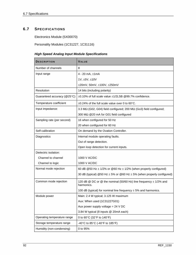
6.7 Specifications
92 REF_1150
6.7 SPECIFICATIONS
Electronics Module (5X00070)
Personality Modules (1C31227, 1C31116)
High Speed Analog Input Module Specifications
DE S C RI P T I O N VAL U E
Number of channels 8
Input range 4 - 20 mA, ±1mA
1V, ±5V, ±10V
±20mV, 50mV, ±100V, ±250mV
Resolution 14 bits (including polarity)
Guaranteed accuracy (@25°C) ±0.10% of full scale value ±1/2LSB @99.7% confidence.
Temperature coefficient ±0.24% of the full scale value over 0 to 60°C.
Input impedance: 3.3 MΩ (G02, G04) field configured; 200 MΩ (Go3) field configured;
300 MΩ @20 mA for G01 field configured
Sampling rate (per second) 16 when configured for 50 Hz
20 when configured for 60 Hz
Self-calibration On demand by the Ovation Controller.
Diagnostics Internal module operating faults.
Out of range detection.
Open loop detection for current inputs.
Dielectric isolation:
Channel to channel
Channel to logic
1000 V AC/DC
1000 V AC/DC
Normal mode rejection 60 dB @50 Hz ± 1/2% or @60 Hz ± 1/2% (when properly configured)
30 dB (typical) @50 Hz ± 5% or @60 Hz ± 5% (when properly configured)
Common mode rejection 120 dB @ DC or @ the nominal (50/60 Hz) line frequency ± 1/2% and harmonics.
100 dB (typical) for nominal line frequency ± 5% and harmonics.
Module power Main: 2.4 W typical; 3.125 W maximum
Aux: When used (1C31227G01)
Aux power supply voltage = 24 V DC
3.84 W typical (8 inputs @ 20mA each)
Operating temperature range 0 to 60°C (32°F to 140°F)
Storage temperature range -40°C to 85°C (-40°F to 185°F)
Humidity (non-condensing) 0 to 95%

REF_1150 93
IN THIS SECTION
Description ........................................................................................................................ 93 Module Group Information ................................................................................................93 Wiring Information .............................................................................................................94 Address Location Information ...........................................................................................96 Diagnostic LEDs................................................................................................................98 Specifications .................................................................................................................... 99
7.1 DESCRIPTION
The Analog Output Electronics Module uses low-power-drain 12-bit serial digital-to-analog converters (DACs) to provide four isolated output channels. The serial clock and data allow the four channels to be updated every 1.5 ms. The serial interface uses opto-isolators for high-voltage isolation.
The Analog Output Module is applicable for CE Mark Certified Systems.
Note: I/O Module General Information (see page 15) contains environmental, installation, wiring, and fuse information for I/O modules.
7.2 MODULE GROUP INFORMATION
7.2.1 ELECTRONICS MODULES (EMODS)
There are four groups of Electronics modules for the Analog Output Module:
1C31129G01 provides voltage output range of 0 to 5 V DC. 1C31129G02 provides voltage output range of 0 to 10 V. 1C31129G03 provides voltage output range of 0 to 20 mA with diagnostics. 1C31129G04 provides voltage output range of 0 to 20 mA without diagnostics.
7.2.2 PERSONALITY MODULE (PMOD)
There is one Personality module group for the Analog Output Module:
1C31132G01 routes field signals from the Electronics module to the terminal block.
S E C T I O N 7
ANALOG OUTPUT MODULE
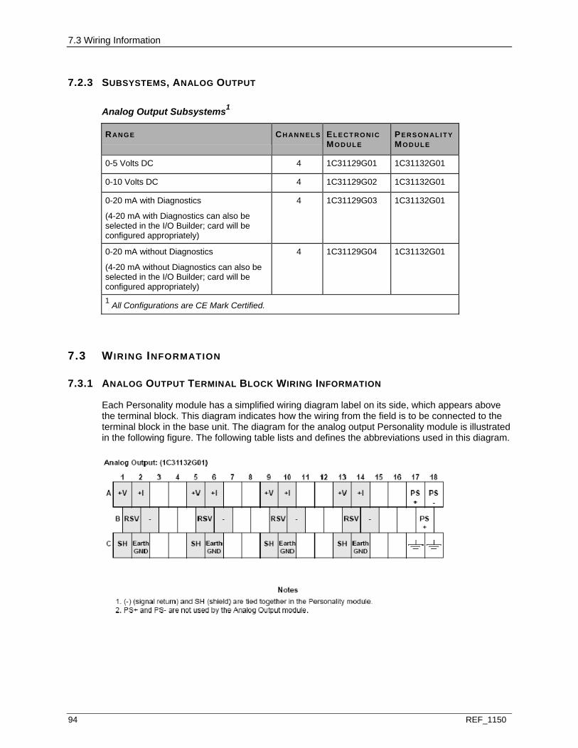
7.3 Wiring Information
94 REF_1150
7.2.3 SUBSYSTEMS, ANALOG OUTPUT
Analog Output Subsystems1
RAN G E CH AN N E L S EL E C T RO NI C MO D U LE
PE R S O N AL I T Y MO D U LE
0-5 Volts DC 4 1C31129G01 1C31132G01
0-10 Volts DC 4 1C31129G02 1C31132G01
0-20 mA with Diagnostics
(4-20 mA with Diagnostics can also be selected in the I/O Builder; card will be configured appropriately)
4 1C31129G03 1C31132G01
0-20 mA without Diagnostics
(4-20 mA without Diagnostics can also be selected in the I/O Builder; card will be configured appropriately)
4 1C31129G04 1C31132G01
1 All Configurations are CE Mark Certified.
7.3 WIRING INFORMATION
7.3.1 ANALOG OUTPUT TERMINAL BLOCK WIRING INFORMATION
Each Personality module has a simplified wiring diagram label on its side, which appears above the terminal block. This diagram indicates how the wiring from the field is to be connected to the terminal block in the base unit. The diagram for the analog output Personality module is illustrated in the following figure. The following table lists and defines the abbreviations used in this diagram.
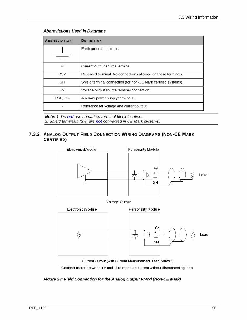
7.3 Wiring Information
REF_1150 95
Abbreviations Used in Diagrams
AB B R E V I AT I ON DE FI N I T I O N
Earth ground terminals.
+I Current output source terminal.
RSV Reserved terminal. No connections allowed on these terminals.
SH Shield terminal connection (for non-CE Mark certified systems).
+V Voltage output source terminal connection.
PS+, PS- Auxiliary power supply terminals.
- Reference for voltage and current output.
Note: 1. Do not use unmarked terminal block locations. 2. Shield terminals (SH) are not connected in CE Mark systems.
7.3.2 ANALOG OUTPUT FIELD CONNECTION WIRING DIAGRAMS (NON-CE MARK CERTIFIED)
Figure 28: Field Connection for the Analog Output PMod (Non-CE Mark)
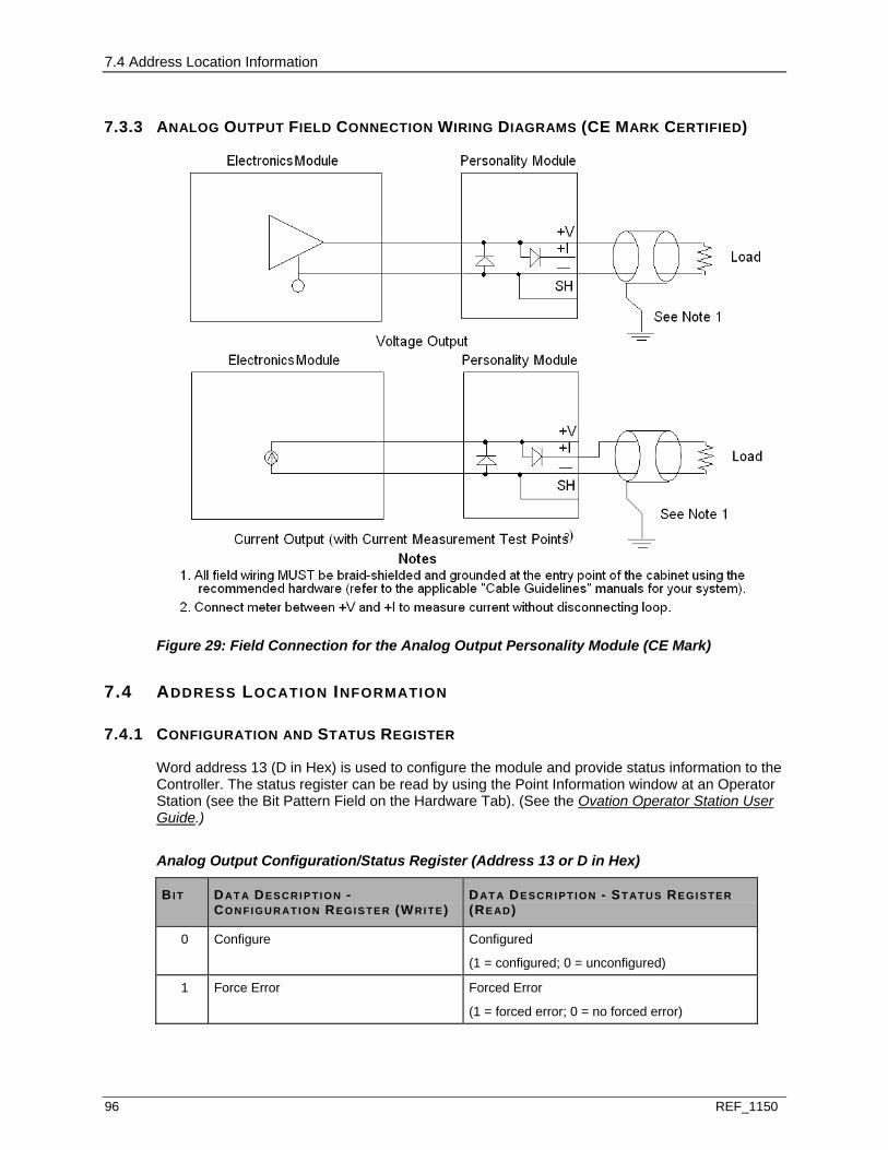
7.4 Address Location Information
96 REF_1150
7.3.3 ANALOG OUTPUT FIELD CONNECTION WIRING DIAGRAMS (CE MARK CERTIFIED)
Figure 29: Field Connection for the Analog Output Personality Module (CE Mark)
7.4 ADDRESS LOCATION INFORMATION
7.4.1 CONFIGURATION AND STATUS REGISTER
Word address 13 (D in Hex) is used to configure the module and provide status information to the Controller. The status register can be read by using the Point Information window at an Operator Station (see the Bit Pattern Field on the Hardware Tab). (See the Ovation Operator Station User Guide.)
Analog Output Configuration/Status Register (Address 13 or D in Hex)
BI T DAT A DE S C R I P T I O N - CO N FI G U R AT I O N REGI S TE R (WRI TE)
DAT A DE S C R I P T I O N - ST AT U S REGI S TER (RE AD)
0 Configure Configured
(1 = configured; 0 = unconfigured)
1 Force Error Forced Error
(1 = forced error; 0 = no forced error)
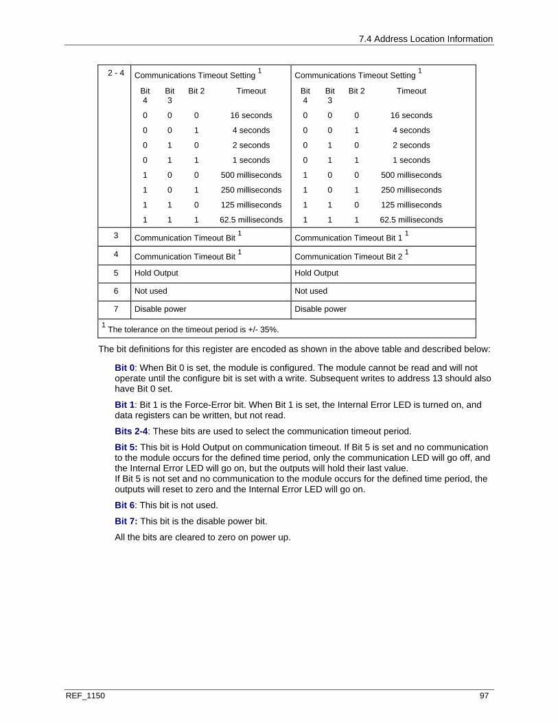
7.4 Address Location Information
REF_1150 97
2 - 4 Communications Timeout Setting 1
Bit 4
Bit 3
Bit 2 Timeout
0 0 0 16 seconds
0 0 1 4 seconds
0 1 0 2 seconds
0 1 1 1 seconds
1 0 0 500 milliseconds
1 0 1 250 milliseconds
1 1 0 125 milliseconds
1 1 1 62.5 milliseconds
Communications Timeout Setting 1
Bit 4
Bit 3
Bit 2 Timeout
0 0 0 16 seconds
0 0 1 4 seconds
0 1 0 2 seconds
0 1 1 1 seconds
1 0 0 500 milliseconds
1 0 1 250 milliseconds
1 1 0 125 milliseconds
1 1 1 62.5 milliseconds 3 Communication Timeout Bit 1 Communication Timeout Bit 1 1
4 Communication Timeout Bit 1 Communication Timeout Bit 2 1
5 Hold Output Hold Output
6 Not used Not used
7 Disable power Disable power
1 The tolerance on the timeout period is +/- 35%.
The bit definitions for this register are encoded as shown in the above table and described below:
Bit 0: When Bit 0 is set, the module is configured. The module cannot be read and will not operate until the configure bit is set with a write. Subsequent writes to address 13 should also have Bit 0 set.
Bit 1: Bit 1 is the Force-Error bit. When Bit 1 is set, the Internal Error LED is turned on, and data registers can be written, but not read.
Bits 2-4: These bits are used to select the communication timeout period.
Bit 5: This bit is Hold Output on communication timeout. If Bit 5 is set and no communication to the module occurs for the defined time period, only the communication LED will go off, and the Internal Error LED will go on, but the outputs will hold their last value. If Bit 5 is not set and no communication to the module occurs for the defined time period, the outputs will reset to zero and the Internal Error LED will go on.
Bit 6: This bit is not used.
Bit 7: This bit is the disable power bit.
All the bits are cleared to zero on power up.

7.5 Diagnostic LEDs
98 REF_1150
7.4.2 OUTPUT CURRENT STATUS REGISTER
The register at address 12 (C in Hex) is for diagnostics and is a read-only register. The overcurrent and undercurrent status bits may be read from this register. The following table shows the overcurrent and undercurrent bits for each channel. The overcurrent bits are used for both the voltage groups and current groups. The undercurrent bits only have meaning for the current group. The voltage output groups do not implement the undercurrent bit.
The simultaneous setting of a channel's overcurrent and undercurrent bits indicates a loss of Field Card power supply for that channel. Overcurrent and undercurrent bits indicate the output current status of this module and not the loop current.
Note: Group 4 current output Field Cards do not have these diagnostic capabilities and the overcurrent and undercurrent bits are strapped in the logical zero state. Since the Group 4 modules do not have diagnostics, the information is not available to the Ovation Controller to support redundancy logic calculations. Groups 1 and 2 do not have undercurrent indication.
Output Current Status Bits (Address 12 or C in Hex)
BI T DE S C RI P T I O N
0 Channel 1 Overcurrent
1 Channel 1 Undercurrent
2 Channel 2 Overcurrent
3 Channel 2 Undercurrent
4 Channel 3 Overcurrent
5 Channel 3 Undercurrent
6 Channel 4 Overcurrent
7 Channel 4 Undercurrent
7.5 DIAGNOSTIC LEDS
The following table lists the module’s LEDs and describes what they mean when lit.
Analog Output Diagnostic LEDs
LED DE S C RI P T I O N
P (Green) Power OK LED. Lit when the +5V power is OK.
C (Green) Communications OK LED. Lit when the Controller is communicating with the module.
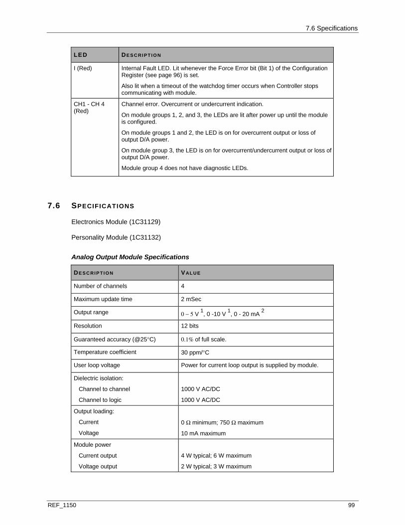
7.6 Specifications
REF_1150 99
LED DE S C RI P T I O N
I (Red) Internal Fault LED. Lit whenever the Force Error bit (Bit 1) of the Configuration Register (see page 96) is set.
Also lit when a timeout of the watchdog timer occurs when Controller stops communicating with module.
CH1 - CH 4 (Red)
Channel error. Overcurrent or undercurrent indication.
On module groups 1, 2, and 3, the LEDs are lit after power up until the module is configured.
On module groups 1 and 2, the LED is on for overcurrent output or loss of output D/A power.
On module group 3, the LED is on for overcurrent/undercurrent output or loss of output D/A power.
Module group 4 does not have diagnostic LEDs.
7.6 SPECIFICATIONS
Electronics Module (1C31129)
Personality Module (1C31132)
Analog Output Module Specifications
DE S C RI P T I O N VAL U E
Number of channels 4
Maximum update time 2 mSec
Output range 0 − 5 V 1, 0 -10 V 1, 0 - 20 mA 2
Resolution 12 bits
Guaranteed accuracy (@25°C) 0.1% of full scale.
Temperature coefficient 30 ppm/°C
User loop voltage Power for current loop output is supplied by module.
Dielectric isolation:
Channel to channel
Channel to logic
1000 V AC/DC
1000 V AC/DC
Output loading:
Current
Voltage
0 Ω minimum; 750 Ω maximum
10 mA maximum
Module power
Current output
Voltage output
4 W typical; 6 W maximum
2 W typical; 3 W maximum

7.6 Specifications
100 REF_1150
DE S C RI P T I O N VAL U E
Operating temperature range 0 to 60°C (32°F to 140°F)
Storage temperature range -40°C to 85°C (-40°F to 185°F)
Humidity (non-condensing) 0 to 95%
1 Overcurrent load indications. 2 Module supplied loop voltage, overcurrent and undercurrent diagnostic indication. Provides the ability to measure current without disconnecting loop.
REF_1150 101
IN THIS SECTION
Description ......................................................................................................................102 Module Group Information ..............................................................................................102 Wiring Information ...........................................................................................................103 Address Location Information .........................................................................................109 Diagnostic LEDs..............................................................................................................110 Specifications ..................................................................................................................111
S E C T I O N 8
CONTACT INPUT MODULE
8.1 Description
102 REF_1150
8.1 DESCRIPTION
The Contact Input Module, comprised of an Electronics module and Personality module, provides 16 contact input current detecting channels with common returns. The field side circuitry and terminal connections (see page 105) for three of these channels are shown (see page 104).
A +48V on-board power supply provides current limited contact wetting voltage if the contact is open. If the contact closes, current is drawn from the +10V supply which turns on the associated opto-isolator; thereby, relaying a closed contact state to the I/O bus. The opto-isolators and the isolation provided by the 10V and 48 Volt power supply provide high dielectric isolation between the field side and the logic or I/O bus side.
There are two methods of wiring field devices to the Contact Input Module termination block (see page 105). Each field contact may have a separate input and return line as shown for channel 1. Alternatively, field contacts wired to the same Contact Input Module may share a return line as shown for channels 2 and 3. For either wiring method, do not tie the contact return line to earth ground or a ground fault condition will occur as well as a degradation of the common mode surge protection.
Debouncing of a contact input signal is done by an RC filter and digital debouncer on the logic side. If a contact changes state for less than 3 msec, the change of state will always be rejected. If the Contact changes state for more than 7 msec, the change of state will always be accepted.
Ground fault detection circuitry on a Contact Input Module activates when an input or return line for any channel finds a low impedance (<5 K ohms) path to earth ground. A single ground fault wire will not cause an error in the point data, but multiple ground faults (if they include input and return lines) could cause faulty data (that is, channels appearing as if contacts are closed when they are really open).
When a ground fault occurs, the external error LED lights, and the GND Fault bit in the Status Register (see page 109) is set. If the GND Fault (see page 105) Attention Enable bit is set in the Configuration Register (see page 109), a ground fault is seen as a catastrophic error causing an attention status to be sent back to the Controller. The Contact Input Module is applicable for CE Mark Certified Systems.
Note: I/O Module General Information (see page 15) contains environmental, installation, wiring, and fuse information for I/O modules.
8.2 MODULE GROUP INFORMATION
8.2.1 ELECTRONICS MODULE (EMOD)
There is one Electronics module group for the Contact Input Module:
1C31142G01 provides 48 VDC on-card auxiliary power for 16 contact inputs with common return.
8.2.2 PERSONALITY MODULE (PMOD)
There is one Personality module group for the Contact Input Module:
1C31110G03 contains surge-protection components for 16 inputs.

8.3 Wiring Information
REF_1150 103
8.2.3 SUBSYSTEMS, CONTACT INPUT
Contact Input Subsystems
RAN G E CH AN N E L S EL E C T RO NI C MO D U LE
PE R S O N AL I T Y MO D U LE
48 VDC On-Card Auxiliary 16 1C31142G01 1C31110G03
All Configurations are CE Mark Certified.
8.3 WIRING INFORMATION
8.3.1 CONTACT INPUT TERMINAL BLOCK WIRING INFORMATION
Each Personality module has a simplified wiring diagram label on its side, which appears above the terminal block. This diagram indicates how the wiring from the field is to be connected to the terminal block in the base unit. The diagram for the contact input Personality module (also known as digital input) is illustrated in the following figure.
Figure 30: Terminal Block Connections for the Contact Input Personality Modules
The following table lists and defines the abbreviations used in this diagram.
Abbreviations Used in Diagrams
AB B R E V I AT I ON DE FI N I T I O N
1+ through 16+ Contact input positive terminal connection
1- through 16- Contact input negative terminal connection
Earth ground terminals
PS+, PS- Auxiliary Power Supply terminals
RSV Reserved terminal. No connection allowed on these terminals

8.3 Wiring Information
104 REF_1150
Note: Do not use terminal block locations marked RSV.
8.3.2 FIELD WIRING RESTRICTIONS:
The following definitions apply to the restrictions listed below:
Rshunt = contact shunt resistance Rcontact = resistance associated with a closed contact Rreturn = resistance of the common return line Rline = resistance of the non-common cable length to and from the contact Rwiring = Rcontact + Rline + 16Rreturn Rfault = resistance from either line to ground which causes a ground fault
Cable resistances (see page 106) that affect contact input performance. The following restrictions apply:
Under no-ground-fault conditions or if the channel return (low) line has a ground fault:
Rshunt across contact must be ≥ 10k ohms to always recognize an open contact as open.
Rshunt across contact must be ≥ 50k ohms to maintain the high level contact-wetting voltage.
If the input connection from a channel has a ground fault with the contact open:
Rshunt across contact must be ≥ 150k ohms to guarantee ground fault is detected. For a ground fault on the input or return connection to a channel:
Rfault from either line to ground must be ≤ 5K ohms to guarantee detection of the ground fault.
With or without ground fault conditions: Rwiring through field wiring to contact must by < 100 ohms to always recognize a closed
contact as closed.
8.3.3 FIELD WIRING CABLE LENGTHS
The following two tables list the maximum cable lengths for field wiring to the contacts. For both, assume Rcontact is 0 ohms.
The following table applies when there are individual common return lines brought to the card edge. This implies that Rreturn is 0 ohms.
Maximum Cable Length for 16 Individual Common Returns
WI R E GAU G E OHM S P E R TH O U S AN D FEE T - (SO LI D CO PPE R WI RE)
MAX I M UM CAB L E LE NG T H - (THO U S AN D S O F FE E T)
18 6.64 7.5
20 10.2 4.9
22 16.2 3.0

8.3 Wiring Information
REF_1150 105
The following table applies when all 16 channels share a common return line. In both tables, the Maximum Cable Length is the length of the cables from the termination block to the contacts in the field.
Maximum Cable Length for a Single Common Return for All 16 Inputs
WI R E GAU G E OHM S P E R TH O U S AN D FEE T - (SO LI D CO PPE R WI RE)
MAX I M UM CAB L E LE NG T H - (THO U S AN D S O F FE E T)
12 1.66 3.54
14 2.27 2.59
16 4.18 1.40
18 6.64 0.89
8.3.4 CONTACT INPUT FRONT END FIELD CONNECTION WIRING DIAGRAMS
Figure 31: Contact Input Module Front End
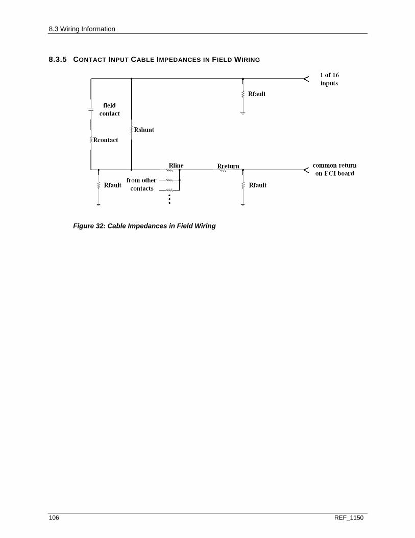
8.3 Wiring Information
106 REF_1150
8.3.5 CONTACT INPUT CABLE IMPEDANCES IN FIELD WIRING
Figure 32: Cable Impedances in Field Wiring
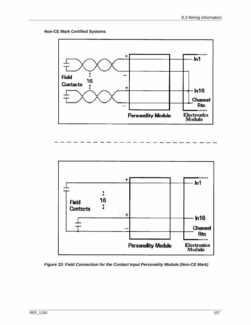
8.3 Wiring Information
REF_1150 107
Non-CE Mark Certified Systems
Figure 33: Field Connection for the Contact Input Personality Module (Non-CE Mark)
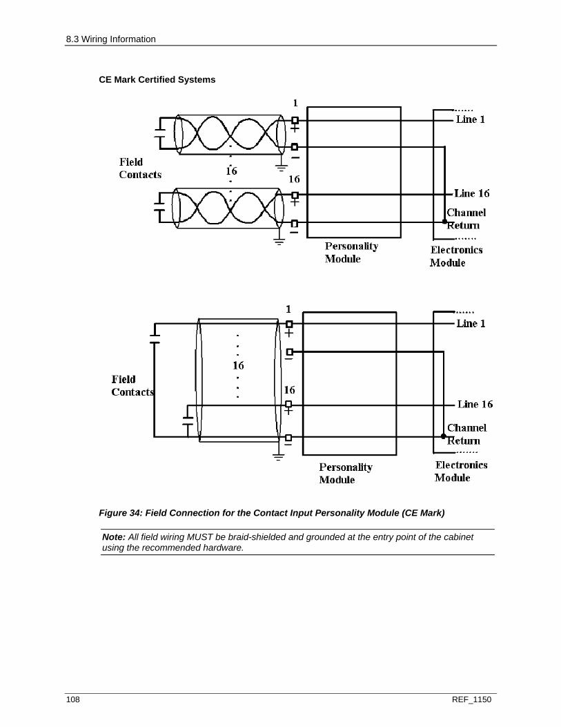
8.3 Wiring Information
108 REF_1150
CE Mark Certified Systems
Figure 34: Field Connection for the Contact Input Personality Module (CE Mark)
Note: All field wiring MUST be braid-shielded and grounded at the entry point of the cabinet using the recommended hardware.
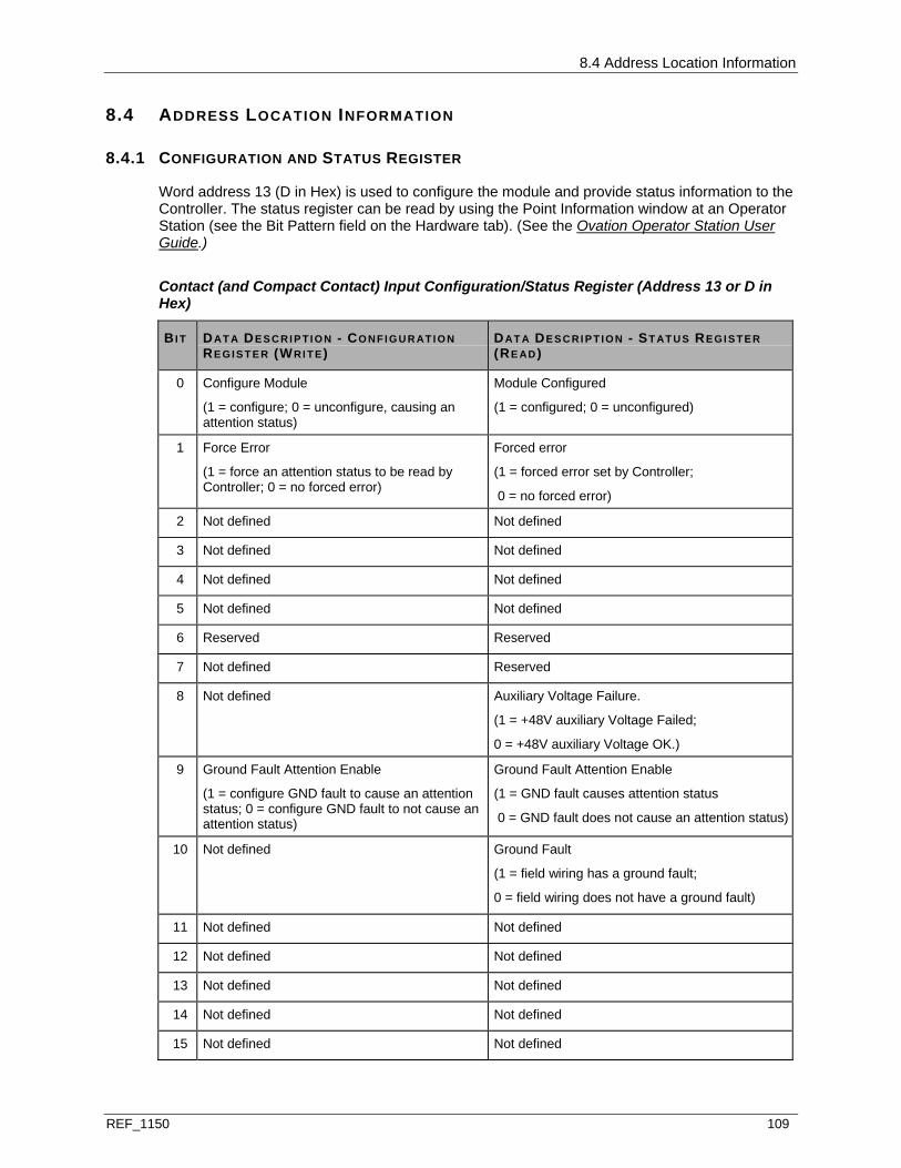
8.4 Address Location Information
REF_1150 109
8.4 ADDRESS LOCATION INFORMATION
8.4.1 CONFIGURATION AND STATUS REGISTER
Word address 13 (D in Hex) is used to configure the module and provide status information to the Controller. The status register can be read by using the Point Information window at an Operator Station (see the Bit Pattern field on the Hardware tab). (See the Ovation Operator Station User Guide.)
Contact (and Compact Contact) Input Configuration/Status Register (Address 13 or D in Hex)
BI T DAT A DE S C R I P T I O N - CO NF I G U R AT I O N RE GI S T E R (WRI T E)
DAT A DE S C R I P T I O N - ST AT U S REGI S TER (RE AD)
0 Configure Module
(1 = configure; 0 = unconfigure, causing an attention status)
Module Configured
(1 = configured; 0 = unconfigured)
1 Force Error
(1 = force an attention status to be read by Controller; 0 = no forced error)
Forced error
(1 = forced error set by Controller;
0 = no forced error)
2 Not defined Not defined
3 Not defined Not defined
4 Not defined Not defined
5 Not defined Not defined
6 Reserved Reserved
7 Not defined Reserved
8 Not defined Auxiliary Voltage Failure.
(1 = +48V auxiliary Voltage Failed;
0 = +48V auxiliary Voltage OK.)
9 Ground Fault Attention Enable
(1 = configure GND fault to cause an attention status; 0 = configure GND fault to not cause an attention status)
Ground Fault Attention Enable
(1 = GND fault causes attention status
0 = GND fault does not cause an attention status)
10 Not defined Ground Fault
(1 = field wiring has a ground fault;
0 = field wiring does not have a ground fault)
11 Not defined Not defined
12 Not defined Not defined
13 Not defined Not defined
14 Not defined Not defined
15 Not defined Not defined
8.5 Diagnostic LEDs
110 REF_1150
The bit definitions for this register are encoded as shown in the above table and described below:
Bit 0: After the Contact Input Module power is cycled, this bit is “0.” A “1” must be written to the Configure Module bit. If the module is not configured in this manner, an attention status will be sent to the Controller upon an attempt to read the point data. The bit may be read back through the Status Register.
Bit 1: The Force Error bit is “0” after the Contact Input module power is cycled. If the Controller sets the Force Error bit, an attention status is issued. The bit may be read back through the Status Register.
Bits 2-5, 7-8, & 10-15: These bits are not defined in the Configuration register and will be read as high in the Status register. These bits cannot be accessed by the Controller during a write to the module.
Bit 6 & 7: These bits are reserved in the Status Register.
Bit 8: This bit is set in the Status Register if the +48V supply on the FCI board fails.
Bit 9: The GND Fault Attention Enable bit is “0” after the Contact Input module power is cycled. This bit must be set by the Controller if a ground fault is to be treated as a catastrophic failure. If Bit 9 is set, a ground fault will cause an attention status to be returned to the Controller upon accessing the module, and no point data can be read. If the bit is not set, a ground fault will not inhibit the Controller from reading point data. In the latter case, if more than one ground fault occurs on the field wiring to a Contact Input Module, false point data may possibly be read on channels with open contacts.
Bit 10: This bit is set in the Status Register if a ground fault occurs in the field wiring.
8.5 DIAGNOSTIC LEDS
The following table lists the module’s LEDs and describes what they mean when lit.
Contact Input Diagnostic LEDs
LED DE S C RI P T I O N
P (Green) Power OK LED. Lit when the +5V power is OK.
C (Green) Communications OK LED. Lit when the Controller is communicating with the module.
E (Red) External Fault LED. Lit when GND Fault bit (Bit 10) of the Status Register (see page 109) is set. This indicates that a ground fault has occurred in the field wiring. An attention status is generated when the External Fault LED is lit only if the GND Fault Attention Enable bit (Bit 9) is set.
I (Red) Internal Fault LED. Lit whenever the Force Error bit (Bit 1) of the Configuration Register is set or when the on-board +48V/+10/V auxiliary power supply fails.
Also lit when a timeout of the watchdog timer occurs when Controller stops communicating with module.
An attention status is always generated when the LED is lit.
CH1 - CH 16 (Green)
Point Status LED. Lit when the input contact of the LED’s corresponding channel is closed.
8.6 Specifications
REF_1150 111
8.6 SPECIFICATIONS
Electronics Module (1C31142)
Personality Module (1C31110)
Contact Input Module Specifications
DE S C RI P T I O N VAL U E
Number of channels 16
On board auxiliary power supply 42 V minimum
55 V maximum
Propagation delay 7 mSec maximum
Contact bounce rejection
Always rejects contact change of state
Always accepts contact change of state
< 3 mSec
> 7 mSec
Closed contact output current 4 mA minimum
8 mA maximum
Diagnostics Internal module operating faults
Ground Fault Detection
Dielectric isolation:
Channel to logic
1000 V AC/DC
Module power 4.56 W typical
4.75 W maximum
Operating temperature range 0 to 60°C (32°F to 140°F)
Storage temperature range -40°C to 85°C (-40°F to 185°F)
Humidity (non-condensing) 0 to 95%


REF_1150 113
IN THIS SECTION
Description ......................................................................................................................114 Module Group Information ..............................................................................................114 Wiring Information ...........................................................................................................115 Address Location Information .........................................................................................122 Diagnostic LEDs..............................................................................................................123 Specifications ..................................................................................................................124
S E C T I O N 9
COMPACT CONTACT INPUT MODULE
9.1 Description
114 REF_1150
9.1 DESCRIPTION
The Compact Contact Input Module, comprised of an Electronics module, provides 16 contact input current detecting channels with common returns.
Additionally, a foam insert that includes a wiring diagram is available for placement in the Personality module cavity in the base unit.
A +48V on-board power supply provides current limited contact wetting voltage if the contact is open. If the contact closes, current is drawn from the +10V supply which turns on the associated opto-isolator; thereby, relaying a closed contact state to the I/O bus. The opto-isolators and the isolation provided by the 10V and 48 Volt power supply provide high dielectric isolation between the field side and the logic or I/O bus side.
There are two methods of wiring field devices to the Compact Contact Input Module termination block (see page 118). Each field contact may have a separate input and return line as shown for channel 1. Alternatively, field contacts wired to the same Contact Input Module may share a return line as shown for channels 2 and 3. For either wiring method, do not tie the contact return line to earth ground or a ground fault condition will occur as well as a degradation of the common mode surge protection.
Debouncing of a contact input signal is done by an RC filter and digital debouncer on the logic side. If a contact changes state for less than 3 msec, the change of state will always be rejected. If the Contact changes state for more than 7 msec, the change of state will always be accepted.
Ground fault detection circuitry on the Compact Contact Input Module activates when the input or return line for any channel finds a low impedance (<5K ohms) path to earth ground. A single wire with a ground fault will not cause an error in the point data, but multiple ground faults, if they include input and return lines, could cause faulty data (that is, channels appearing as if their contacts are closed when they are really open).
When a ground fault occurs, the external error LED lights, and the GND Fault bit in the Status Register is set. If the GND Fault Attention Enable bit is set in the Configuration Register, a ground fault (see page 118) is seen as a catastrophic error causing an attention status to be sent back to the Controller.
The Compact Contact Input module is applicable for CE Mark certified systems.
Note: I/O Module General Information (see page 15) contains environmental, installation, wiring, and fuse information for I/O modules.
9.2 MODULE GROUP INFORMATION
9.2.1 ELECTRONICS MODULE (EMOD)
There is one Electronics module group for the Compact Contact Input module:
1C31234G01 provides 48 VDC on-card auxiliary power for 16 contact inputs with common return.

9.3 Wiring Information
REF_1150 115
9.2.2 FOAM INSERT
There is no Personality module for the Compact Contact Input module. A foam insert is available that fits into the Personality module cavity in the Base Unit and provides wiring information.
1C31238H01
9.2.3 SUBSYSTEMS, COMPACT CONTACT INPUT
Compact Contact Input Subsystems 1
RAN G E CH AN N E L S EL E C T RO NI C MO D U LE
CAV I T Y
IN S E R T 2
Compact Contact with 48 VDC On-Card Auxiliary 16 1C31234G01 1C31238H01
1 All Configurations are CE Mark Certified. 2 This is an insert that fits into the Personality module position and provides a wiring schematic label for the module. There is no actual Personality module required for this module type.
9.3 WIRING INFORMATION
9.3.1 COMPACT CONTACT INPUT TERMINAL BLOCK WIRING INFORMATION
The available foam insert has a simplified wiring diagram label on its top, which appears above the terminal block. This diagram indicates how the wiring from the field is to be connected to the terminal block in the base unit. The diagram for the Compact Contact Input module is illustrated in the following figure. The following table lists and defines the abbreviations used in this diagram.
Figure 35: Terminal Block Connections for the Compact Contact Input Modules
Abbreviations Used in Diagrams
AB B R E V I AT I ON DE FI N I T I O N
1+ through 16+ Contact input positive terminal connection
1- through 16- Contact input negative terminal connection
Earth ground terminals

9.3 Wiring Information
116 REF_1150
AB B R E V I AT I ON DE FI N I T I O N
PS+, PS- Auxiliary Power Supply terminals
RSV Reserved terminal. No internal connection
9.3.2 FIELD WIRING RESTRICTIONS:
The following definitions apply to the restrictions listed below:
Rshunt = contact shunt resistance Rcontact = resistance associated with a closed contact Rreturn = resistance of the common return line Rline = resistance of the non-common cable length to and from the contact Rwiring = Rcontact + Rline + 16Rreturn Rfault = resistance from either line to ground which causes a ground fault
Cable resistances (see page 119) that affect contact input performance. The following restrictions apply:
Under no-ground-fault conditions or if the channel return (low) line has a ground fault:
Rshunt across contact must be ≥ 10k ohms to always recognize an open contact as open.
Rshunt across contact must be ≥ 50k ohms to maintain the high level contact-wetting voltage.
If the input connection from a channel has a ground fault with the contact open:
Rshunt across contact must be ≥ 150k ohms to guarantee ground fault is detected. For a ground fault on the input or return connection to a channel:
Rfault from either line to ground must be ≤ 5K ohms to guarantee detection of the ground fault.
With or without ground fault conditions: Rwiring through field wiring to contact must by < 100 ohms to always recognize a closed
contact as closed.
9.3.3 FIELD WIRING CABLE LENGTHS
The following two tables list the maximum cable lengths for field wiring to the contacts. For both, assume Rcontact is 0 ohms.
The following table applies when there are individual common return lines brought to the card edge. This implies that Rreturn is 0 ohms.
9.3 Wiring Information
REF_1150 117
Maximum Cable Length for 16 Individual Common Returns
WI R E GAU G E OHM S P E R TH O U S AN D FEE T - (SO LI D CO PPE R WI RE)
MAX I M UM CAB L E LE NG T H - (THO U S AN D S O F FE E T)
18 6.64 7.5
20 10.2 4.9
22 16.2 3.0
The following table applies when all 16 channels share a common return line. In both tables, the Maximum Cable Length is the length of the cables from the termination block to the contacts in the field.
Maximum Cable Length for a Single Common Return for All 16 Inputs
WI R E GAU G E OHM S P E R TH O U S AN D FEE T - (SO LI D CO PPE R WI RE)
MAX I M UM CAB L E LE NG T H - (THO U S AN D S O F FE E T)
12 1.66 3.54
14 2.27 2.59
16 4.18 1.40
18 6.64 0.89

9.3 Wiring Information
118 REF_1150
9.3.4 COMPACT CONTACT INPUT FRONT END FIELD CONNECTION WIRING DIAGRAMS
Figure 36: Compact Contact Input Module Front End

9.3 Wiring Information
REF_1150 119
9.3.5 COMPACT CONTACT INPUT CABLE IMPEDANCES IN FIELD WIRING
Figure 37: Cable Impedances in Field Wiring

9.3 Wiring Information
120 REF_1150
Non-CE Mark Certified Systems
Figure 38: Field Connection for the Compact Contact Input Module (Non-CE Mark)

9.3 Wiring Information
REF_1150 121
CE Mark Certified Systems
Figure 39: Field Connection for the Compact Contact Input Module (CE Mark)

9.4 Address Location Information
122 REF_1150
9.4 ADDRESS LOCATION INFORMATION
9.4.1 CONFIGURATION AND STATUS REGISTER
Word address 13 (D in Hex) is used to configure the module and provide status information to the Controller. The status register can be read by using the Point Information window at an Operator Station (see Bit Pattern field on the Hardware tab). (See Ovation Operator Station User Guide.)
Contact (and Compact Contact) Input Configuration/Status Register (Address 13 or D in Hex)
BI T DAT A DE S C R I P T I O N - CO NF I G U R AT I O N RE GI S T E R (WRI T E)
DAT A DE S C R I P T I O N - ST AT U S REGI S TER (RE AD)
0 Configure Module
(1 = configure; 0 = unconfigure, causing an attention status)
Module Configured
(1 = configured; 0 = unconfigured)
1 Force Error
(1 = force an attention status to be read by Controller; 0 = no forced error)
Forced error
(1 = forced error set by Controller; 0 = no forced error)
2 Not defined Not defined
3 Not defined Not defined
4 Not defined Not defined
5 Not defined Not defined
6 Reserved Reserved
7 Not defined Reserved
8 Not defined Auxiliary Voltage Failure.
(1 = +48V auxiliary Voltage Failed;
0 = +48V auxiliary Voltage OK.)
9 Ground Fault Attention Enable
(1 = configure GND fault to cause an attention status; 0 = configure GND fault to not cause an attention status)
Ground Fault Attention Enable
(1 = GND fault causes attention status
0 = GND fault does not cause an attention status)
10 Not defined Ground Fault
(1 = field wiring has a ground fault;
0 = field wiring does not have a ground fault)
11 Not defined Not defined
12 Not defined Not defined
13 Not defined Not defined
14 Not defined Not defined
15 Not defined Not defined

9.5 Diagnostic LEDs
REF_1150 123
The bit definitions for this register are encoded as shown in the above table and described below:
Bit 0: After the Contact Input Module power is cycled, this bit is “0.” A “1” must be written to the Configure Module bit. If the module is not configured in this manner, an attention status will be sent to the Controller upon an attempt to read the point data. The bit may be read back through the Status Register.
Bit 1: The Force Error bit is “0” after the Contact Input module power is cycled. If the Controller sets the Force Error bit, an attention status is issued. The bit may be read back through the Status Register.
Bits 2-5, 7-8, & 10-15: These bits are not defined in the Configuration register and will be read as high in the Status register. These bits cannot be accessed by the Controller during a write to the module.
Bit 6 & 7: These bits are reserved in the Status Register.
Bit 8: This bit is set in the Status Register if the +48V supply on the FCI board fails.
Bit 9: The GND Fault Attention Enable bit is “0” after the Contact Input module power is cycled. This bit must be set by the Controller if a ground fault is to be treated as a catastrophic failure. If Bit 9 is set, a ground fault will cause an attention status to be returned to the Controller upon accessing the module, and no point data can be read. If the bit is not set, a ground fault will not inhibit the Controller from reading point data. In the latter case, if more than one ground fault occurs on the field wiring to a Contact Input Module, false point data may possibly be read on channels with open contacts.
Bit 10: This bit is set in the Status Register if a ground fault occurs in the field wiring.
9.5 DIAGNOSTIC LEDS
The following table lists the module’s LEDs and describes what they mean when lit.
Compact Contact Input Diagnostic LEDs
LED DE S C RI P T I O N
P (Green) Power OK LED. Lit when the +5V power is OK
C (Green) Communications OK LED. Lit when the Controller is communicating with the module.
E (Red) External Fault LED. Lit when GND Fault bit (Bit 10) of the Status Register is set. This indicates that a ground fault has occurred in the field wiring. An attention status is generated when the External Fault LED is lit only if the GND Fault Attention Enable bit (Bit 9) is set.
I (Red) Internal Fault LED. Lit whenever the Force Error bit (Bit 1) of the Configuration Register is set or when the on-board +48V/+10/V auxiliary power supply fails. Also lit when a timeout of the watchdog timer occurs when Controller stops communicating with module. An attention status is always generated when the LED is lit.
CH1 - CH 16 (Green)
Point Status LED. Lit when the input contact of the LED’s corresponding channel is closed.
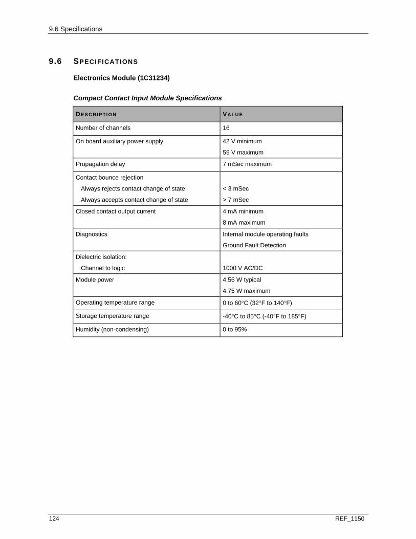
9.6 Specifications
124 REF_1150
9.6 SPECIFICATIONS
Electronics Module (1C31234)
Compact Contact Input Module Specifications
DE S C RI P T I O N VAL U E
Number of channels 16
On board auxiliary power supply 42 V minimum
55 V maximum
Propagation delay 7 mSec maximum
Contact bounce rejection
Always rejects contact change of state
Always accepts contact change of state
< 3 mSec
> 7 mSec
Closed contact output current 4 mA minimum
8 mA maximum
Diagnostics Internal module operating faults
Ground Fault Detection
Dielectric isolation:
Channel to logic
1000 V AC/DC
Module power 4.56 W typical
4.75 W maximum
Operating temperature range 0 to 60°C (32°F to 140°F)
Storage temperature range -40°C to 85°C (-40°F to 185°F)
Humidity (non-condensing) 0 to 95%
REF_1150 125
IN THIS SECTION
Description ......................................................................................................................125 Module Group Information ..............................................................................................125 Module Specific Information............................................................................................127 Wiring Information ...........................................................................................................129 Address Location Information .........................................................................................133 Diagnostic LEDs..............................................................................................................134 Specifications ..................................................................................................................135
10.1 DESCRIPTION
The Digital Input module contains 16 channels where each channel has voltage level sensing circuitry used to detect whether an input is on or off. The module is available with 16 isolated differential inputs, or 16 single-ended (common return) digital inputs with on-card blown fuse detection for the auxiliary power supply. The selection of the personality module determines if the inputs are differential or single-ended. The input voltage level monitored by the module is determined by the particular card group in the module.
The field side circuitry for the single ended configuration (see page 127), and for the differential configuration (see page 128) are described in their respective sections An input resistor provides the normal mode surge protection and limits the current during normal operation. An opto-isolator provides high dielectric isolation between the field side and the logic or I/O bus side.
The Single-Ended Digital Input configuration has a circuit used to monitor the presence of the auxiliary supply. Two cases cause this monitor circuitry to report a blown fuse status and issue an attention status to the Ovation Controller:
Fuse is blown on the Personality Module. Auxiliary supply level is lower than minimum On Input Voltage.
Note: I/O Module General Information (see page 15) contains environmental, installation, wiring, and fuse information for I/O modules.
10.2 MODULE GROUP INFORMATION
10.2.1 ELECTRONICS MODULES (EMODS)
There are two Electronics module for the Digital Input Module:
1C31107G01 provides for 24/48 VAC/VDC single-ended or differential inputs. 1C31107G02 provides for 125 VAC/VDC single-ended or differential inputs.
S E C T I O N 1 0
DIGITAL INPUT MODULE
10.2 Module Group Information
126 REF_1150
10.2.2 PERSONALITY MODULES (PMODS)
There are two Personality module groups for the Digital Input Module:
1C31110G01 provides for single-ended inputs. 1C31110G02 provides for differential inputs.
10.2.3 SUBSYSTEMS, DIGITAL INPUT
Digital Input Subsystems 1
RAN G E CH AN N E L S EL E C T RO NI C MO D U LE
PE R S O N AL I T Y MO D U L E
24/48 VAC/VDC
Single-ended
Differential
16
16
1C31107G01
1C31107G01
1C31110G01
1C31110G02
125 VAC/VDC
Single-ended
Differential
16
16
1C31107G02
1C31107G02
1C31110G01
1C31110G02 1 All configurations are CE Mark Certified.
When the 125VAC/VDC Digital Input Emod (1C31107G02) is used in applications without the Fused Pmod (5X00034G01), additional external fusing or other current limiting devices are recommended on the hazardous inputs to provide additional protection to the external wiring and power source.
CAUTION! CE Mark certified systems, Any base unit that contains a 125VAC/DC Digital Input Electronics module (1C31107G02) with a Differential Digital Input Personality Module (1C31110G02) and interfaces to hazardous voltage (>30 V RMS, 42.4 V peak, or 60 VDC) must include a hazardous voltage warning label (1B30025H01) on that base unit.
Any base unit that contains a 125VAC/DC Digital Input Electronics module (1C31107G02) with a Single-ended Digital Input Personality Module (1C31110G01) and interfaces to hazardous voltage (>30 V RMS, 42.4 V peak, or 60 VDC) must include a hazardous voltage warning label (1B30025H01) on ALL base units on the branch.
This label must be placed in a visible location on the base unit, preferably above the spare fuse location. The project drawings must indicate this.
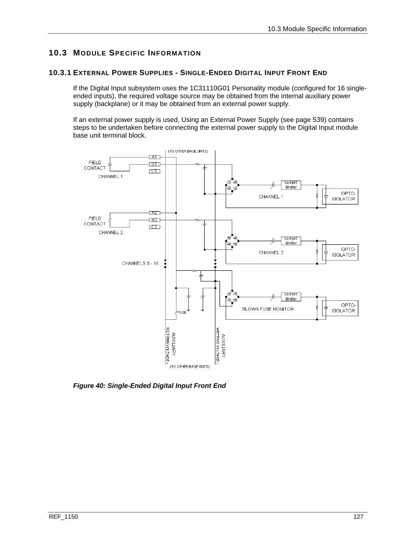
10.3 Module Specific Information
REF_1150 127
10.3 MODULE SPECIFIC INFORMATION
10.3.1 EXTERNAL POWER SUPPLIES - SINGLE-ENDED DIGITAL INPUT FRONT END
If the Digital Input subsystem uses the 1C31110G01 Personality module (configured for 16 single-ended inputs), the required voltage source may be obtained from the internal auxiliary power supply (backplane) or it may be obtained from an external power supply.
If an external power supply is used, Using an External Power Supply (see page 539) contains steps to be undertaken before connecting the external power supply to the Digital Input module base unit terminal block.
Figure 40: Single-Ended Digital Input Front End
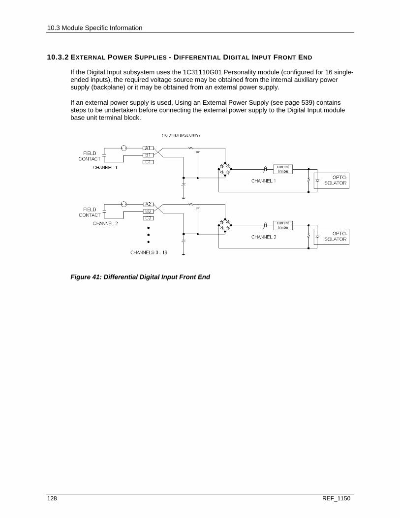
10.3 Module Specific Information
128 REF_1150
10.3.2 EXTERNAL POWER SUPPLIES - DIFFERENTIAL DIGITAL INPUT FRONT END
If the Digital Input subsystem uses the 1C31110G01 Personality module (configured for 16 single-ended inputs), the required voltage source may be obtained from the internal auxiliary power supply (backplane) or it may be obtained from an external power supply.
If an external power supply is used, Using an External Power Supply (see page 539) contains steps to be undertaken before connecting the external power supply to the Digital Input module base unit terminal block.
Figure 41: Differential Digital Input Front End
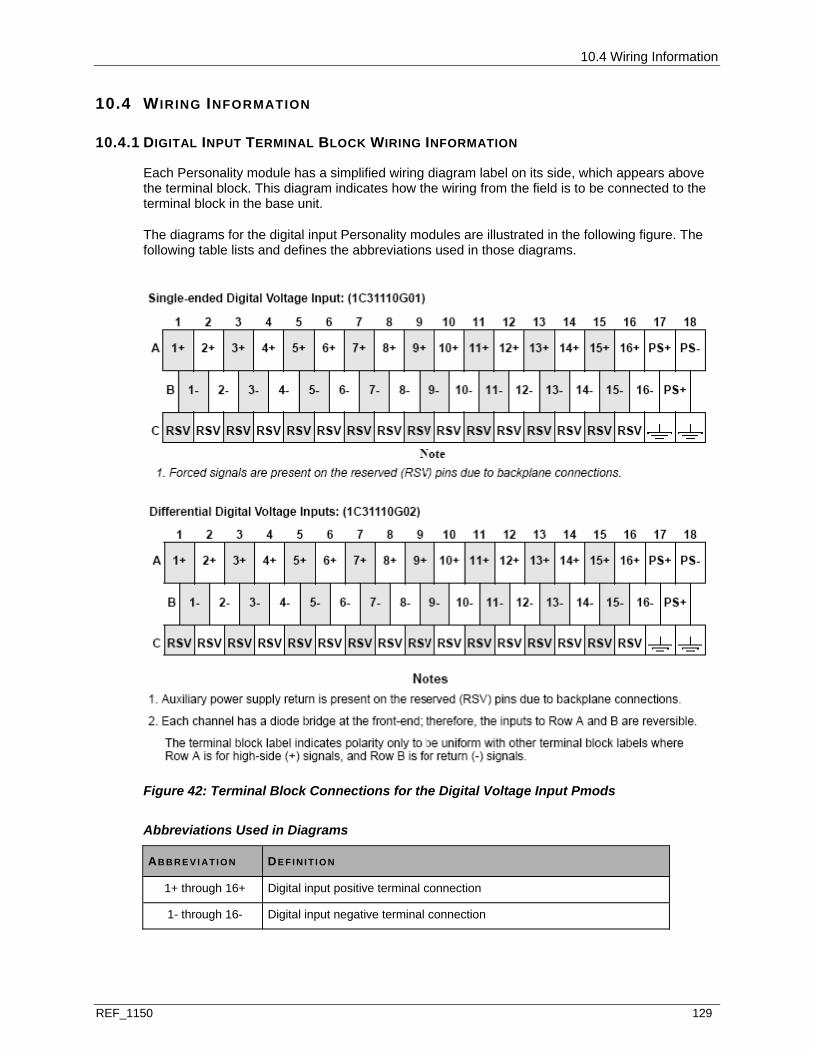
10.4 Wiring Information
REF_1150 129
10.4 WIRING INFORMATION
10.4.1 DIGITAL INPUT TERMINAL BLOCK WIRING INFORMATION
Each Personality module has a simplified wiring diagram label on its side, which appears above the terminal block. This diagram indicates how the wiring from the field is to be connected to the terminal block in the base unit.
The diagrams for the digital input Personality modules are illustrated in the following figure. The following table lists and defines the abbreviations used in those diagrams.
Figure 42: Terminal Block Connections for the Digital Voltage Input Pmods
Abbreviations Used in Diagrams
AB B R E V I AT I ON DE FI N I T I O N
1+ through 16+ Digital input positive terminal connection
1- through 16- Digital input negative terminal connection

10.4 Wiring Information
130 REF_1150
AB B R E V I AT I ON DE FI N I T I O N
Earth ground terminals
PS+, PS- Auxiliary Power Supply terminals
RSV Reserved terminal. No connection allowed on these terminals
Do not use terminal block locations marked RSV.
10.4.2 FIELD WIRING CONSIDERATIONS FOR THE DIGITAL INPUT CONFIGURATION
The following maximum resistances of the cable and the interfaced device apply:
24/48VDC - 175 KΩ 24 VAC - 50 KΩ 125 VDC - 250 KΩ 125 VAC - 50 KΩ

10.4 Wiring Information
REF_1150 131
10.4.3 NON-CE MARK CERTIFIED SYSTEMS
Single-Ended Digital Voltage Inputs
Differential Digital Voltage Inputs
1C31110G01 Personality Module
1C31110G02 Personality Module
ElectronicsModule
ElectronicsModuleAuxiliary
VoltageSupplies
In1
Rtn1
In16
Rtn16
PowerMonitor
Rtn
In1
Rtn1
In16
Rtn16
Channel1
Channel1
Channel16
Channel16
Figure 43: Field Connection for the Digital Input Personality Module (Non-CE Mark)
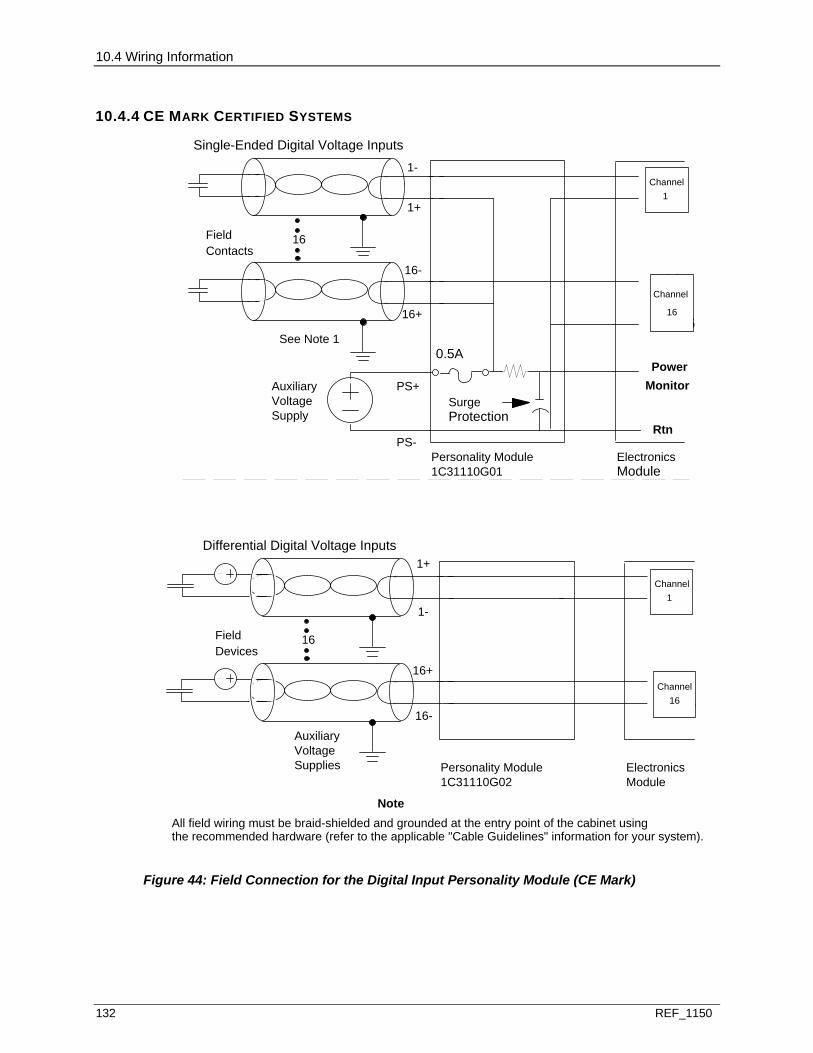
10.4 Wiring Information
132 REF_1150
10.4.4 CE MARK CERTIFIED SYSTEMS
Field
Single-Ended Digital Voltage Inputs
See Note 1
Contacts16
PS+
PS-
1-
1+
16-
16+
Rtn1
In1
Rtn16
In16
PowerMonitor
Rtn
Personality Module ElectronicsModule1C31110G01
SurgeProtection
AuxiliaryVoltageSupply
0.5A
Field
Differential Digital Voltage Inputs
Devices16
1-
1+
16-
16+
Rtn1
In1
Rtn16
In16
Personality Module ElectronicsModule1C31110G02
AuxiliaryVoltageSupplies
All field wiring must be braid-shielded and grounded at the entry point of the cabinet usingNote
the recommended hardware (refer to the applicable "Cable Guidelines" information for your system).
In1
Rtn
Rtn16
Rtn16
Rtn16
In16
In16
PowerMonitor
Rtn1
In1
In1
Channel1
Channel1
Channel16
Channel
16
Figure 44: Field Connection for the Digital Input Personality Module (CE Mark)
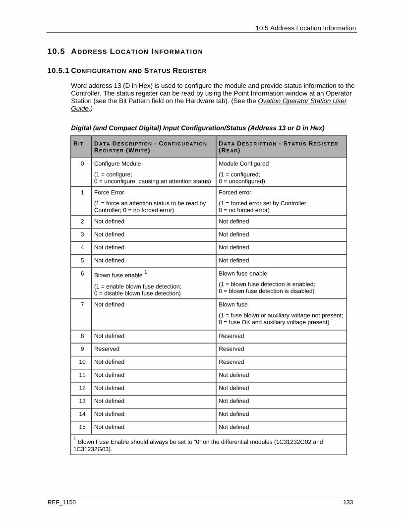
10.5 Address Location Information
REF_1150 133
10.5 ADDRESS LOCATION INFORMATION
10.5.1 CONFIGURATION AND STATUS REGISTER
Word address 13 (D in Hex) is used to configure the module and provide status information to the Controller. The status register can be read by using the Point Information window at an Operator Station (see the Bit Pattern field on the Hardware tab). (See the Ovation Operator Station User Guide.)
Digital (and Compact Digital) Input Configuration/Status (Address 13 or D in Hex)
BI T DAT A DE S C R I P T I O N - CO NF I G U R AT I O N RE GI S T E R (WRI T E)
DAT A DE S C R I P T I O N - ST AT U S REGI S TER (RE AD)
0 Configure Module
(1 = configure; 0 = unconfigure, causing an attention status)
Module Configured
(1 = configured; 0 = unconfigured)
1 Force Error
(1 = force an attention status to be read by Controller; 0 = no forced error)
Forced error
(1 = forced error set by Controller; 0 = no forced error)
2 Not defined Not defined
3 Not defined Not defined
4 Not defined Not defined
5 Not defined Not defined
6 Blown fuse enable 1
(1 = enable blown fuse detection; 0 = disable blown fuse detection)
Blown fuse enable
(1 = blown fuse detection is enabled; 0 = blown fuse detection is disabled)
7 Not defined Blown fuse
(1 = fuse blown or auxiliary voltage not present; 0 = fuse OK and auxiliary voltage present)
8 Not defined Reserved
9 Reserved Reserved
10 Not defined Reserved
11 Not defined Not defined
12 Not defined Not defined
13 Not defined Not defined
14 Not defined Not defined
15 Not defined Not defined
1 Blown Fuse Enable should always be set to “0” on the differential modules (1C31232G02 and 1C31232G03).
10.6 Diagnostic LEDs
134 REF_1150
Bit definitions for this register are encoded as shown in the table above and described below:
Bit 0: After the Compact Digital Input Module power is cycled, this bit is “0.” A “1” must be written to this bit. If the module is not configured in this manner, an attention status will be sent to the Controller upon an attempt to read the point data.
Bit 1: This bit is “0” after the Compact Digital Input Module power is cycled. If the Controller sets this bit, an attention status is issued.
Bits 2-5, 11-15: These bits are not defined in the Configuration register and will be read as high in the Status register.
Bit 6: The Blown Fuse Enable bit is “0” after the Digital Input module power is cycled. This bit must be set by the Controller for Compact Digital Input Modules, using the single-ended personality module, to detect a blown auxiliary power supply fuse when it reads the Status Register. Blown Fuse Enable should always be set to “0”on the differential modules (1C31232G02 and 1C31232G03). The bit may be read back through the Module Status Register.
Bit 7: This bit is set in the Status Register only if the Blown Fuse Enable bit (6) is set and the single-ended on-board auxiliary supply fuse has blown or the auxiliary voltage is not present. This bit is not defined in the Configuration Register.
Bit 8, 10: These bits are reserved in the Status Register. These bits are not defined in the Configuration Register.
Bit 9: This bit is reserved.
10.6 DIAGNOSTIC LEDS
The following table lists the module’s LEDs and describes what they mean when lit.
Digital Input Diagnostic LEDs
LED DE S C RI P T I O N
P (Green) Power OK LED. Lit when the +5V power is OK.
C (Green) Communications OK LED. Lit when the Controller is communicating with the Digital Input module.
E (Red) External Fault LED. Lit when the Blown Fuse bit (Bit 7) of the Status Register is set. This indicates the field supply fuse is blown or the auxiliary power supply is not present. This LED should never light if the Digital Input module is installed since the Blown Fuse Enable bit (Bit 6) of the Status Register should be set to the inactive state by the Controller.
I (Red) Internal Fault LED. Lit whenever the Force Error bit (Bit 1) of the Configuration Register (see page 48) is active or when a timeout of the watchdog timer occurs when the Controller stops communicating with the module.
CH1 - CH 16 (Green)
Point Status LED. Lit when the input voltage of the LED’s corresponding channel is greater than the channel’s minimum On Input Voltage.

10.7 Specifications
REF_1150 135
10.7 SPECIFICATIONS
Electronics Module (1C31107)
Personality Module (1C31110)
Digital Input Module Specifications
DE S C RI P T I O N VAL U E
Number of channels 16
Input range (single-ended or differential) 1 Refer to the table below.
Propagation delay of contact change of state 2
24V/48V DC
24VAC
125VDC
125VAC
1.9 mSec minimum; 25.5 mSec maximum
1.9 mSec minimum; 17.0 mSec maximum
1.9 mSec minimum; 35.0 mSec maximum
1.9 mSec minimum; 40.0 mSec maximum
Cable length (quality is 50pF/ft or better) 1000 feet maximum @ 50pF/ft or better
Diagnostics Internal module operating faults.
Blown fuse detection. 3
Dielectric isolation:
Channel to channel 4
Channel to logic
1000V DC 500V AC
1000V AC/DC
Module power (drawn from logic supply) Main: 1.1 W typical, 1.5 W maximum
Operating temperature range 0 to 60°C (32°F to 140°F)
Storage temperature range -40°C to 85°C (-40°F to 185°F)
Humidity (non-condensing) 0 to 95%
1 Input range level is dependent on module group. 2 Does not include cable capacitance. 3 Blown fuse detection applies to single-ended channel configuration only, where an on-board fuse is provided for the auxiliary power supply. 4 Channel to channel isolation applies to differential channel configuration only.
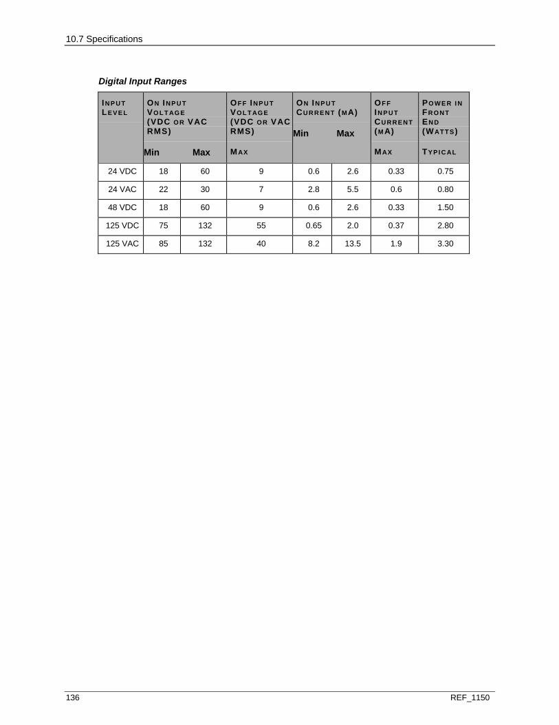
10.7 Specifications
136 REF_1150
Digital Input Ranges
IN P U T LEV E L
ON INP U T VO L T AG E (VDC O R VAC RMS)
Min Max
OF F INP U T VO L T AG E (VDC O R VACRMS)
MAX
ON INP U T CU R R E N T (MA)
Min Max
OF F IN P U T CU R R E N T (M A)
MAX
PO WE R I N FR O NT EN D (WAT T S)
TYPI C AL
24 VDC 18 60 9 0.6 2.6 0.33 0.75
24 VAC 22 30 7 2.8 5.5 0.6 0.80
48 VDC 18 60 9 0.6 2.6 0.33 1.50
125 VDC 75 132 55 0.65 2.0 0.37 2.80
125 VAC 85 132 40 8.2 13.5 1.9 3.30
REF_1150 137
IN THIS SECTION
Description ......................................................................................................................137 Module Group Information ..............................................................................................138 Module Specific Information............................................................................................139 Wiring Information ...........................................................................................................139 Address Location Information .........................................................................................147 Diagnostic LEDs..............................................................................................................148 Specifications ..................................................................................................................149
11.1 DESCRIPTION
The Compact Digital Input module contains 16 channels where each channel has voltage level sensing circuitry used to detect whether an input is on or off. The input voltage level sensed by the module is determined by the particular card group of the module.
The module is available for three options:
16 isolated differential inputs (unfused) (24/48 VAC/VDC or 125 VAC/VDC). 16 single-ended (common return) digital inputs with a common fuse and on-card blown fuse
detection for the auxiliary power supply (24/48 VDC). 16 individually fused digital inputs using a common power supply. Blown fuse detection is not
available with this option (24/48 VAC/VDC or 125 VAC/VDC).
The field side circuitry for the single-ended configuration (see page 141) and for the differential configuration (see page 142). The field side circuitry for the 16 individually fused configuration (see page 143). An input resistor provides the normal mode surge protection and limits the current during normal operation. An opto-isolator provides high dielectric isolation between the field side and the logic or I/O bus side.
The Single-Ended Digital Input configuration has a circuit used to monitor the presence of the auxiliary supply (blown fuse detection). Two cases cause this monitor circuitry to report a blown fuse status and issue an attention status to the Ovation Controller:
Fuse is blown on the Electronics Module. Auxiliary supply level is lower than minimum On Input Voltage.
In addition, a foam insert that includes a wiring diagram is available for placement in the Personality module cavity in the Base Unit in all configurations except the 16 point individually fused option which requires a personality module (5X00034). The compact digital input module is applicable for CE Mark certified systems
Note: I/O Module General Information (see page 15) contains environmental, installation, wiring, and fuse information for I/O modules.
S E C T I O N 1 1
COMPACT DIGITAL INPUT MODULE

11.2 Module Group Information
138 REF_1150
11.2 MODULE GROUP INFORMATION
11.2.1 ELECTRONICS MODULES (EMODS)
There are three Electronics module groups for the Compact Digital Input Module:
1C31232G01 provides for 24/48 VDC single-ended inputs. 1C31232G02 provides for 24/48 VAC/VDC differential inputs and supports the 16 point
individually fused option. 1C31232G03 provides for 125 VAC/VDC differential inputs and supports the 16 point
individually fused option.
11.2.2 PERSONALITY MODULE (PMOD)
There is one Personality module group for the Compact Digital Input Module:
5X00034G01 provides for 16 point individual fusing with a common supply. This is an optional Personality module that is available for use with the differential input Electronics modules (1C31232G02, 1C31232G03) for applications requiring individual point fusing with a common supply.
Note: This Personality Module is not available for use with Single Ended Electronics Module 1C3123G01.
11.2.3 FOAM INSERT
In the event that individual fusing is not required, a foam insert is available that fits into the Personality module cavity in the Base Unit and provides wiring information.
1C31238H01
11.2.4 SUBSYSTEMS, COMPACT DIGITAL INPUT
Compact Digital Input Subsystems 1
RAN G E CH AN N E L S EL E C T RO NI C MO D U LE
PE R S O N AL I T Y MODULE OR CAV I T Y
IN S E R T 2
24/48 VDC
Single-ended
16
1C31232G01
1C31238H011 (Cavity Insert)
24 VAC/VDC
48 VAC/VDC
Differential
16
1C31232G02
5X00034G01(Fused Pmod)
1C31238H011 (Cavity Insert)
125 VAC/VDC
Differential
16
1C31232G03
5X00034G01 (Fused Pmod)
1C31238H011 (Cavity Insert)

11.3 Module Specific Information
REF_1150 139
RAN G E CH AN N E L S EL E C T RO NI C MO D U LE
PE R S O N AL I T Y MODULE OR CAV I T Y
IN S E R T 2
1All Configurations are CE Mark Certified. 2 This is an insert that fits into the Personality module position and provides a wiring schematic label for the module.
When the 125VAC/VDC Compact Digital Input Emod (1C31232G03) is used in applications without the Fused Pmod (5X00034G01), additional external fusing or other current limiting devices are recommended on the hazardous inputs to provide additional protection to the external wiring and power source.
11.3 MODULE SPECIFIC INFORMATION
11.3.1 EXTERNAL POWER SUPPLIES
The required voltage source may be obtained from the internal auxiliary power supply (backplane) or it may be obtained from an external power supply when using the following modules:
1C31232G01 single-ended Electronic module (configured for 16 single-ended inputs). 1C31232G02 or 1C31232G03 16 point individually fused configuration Electronic modules
with 5X00034 Personality module.
If an external power supply is used, Using an External Power Supply (see page 539) contains steps to be undertaken before connecting the external power supply to the Compact Digital Input module base unit terminal block.
11.4 WIRING INFORMATION
11.4.1 COMPACT DIGITAL INPUT TERMINAL BLOCK WIRING INFORMATION
The available foam insert or Personality module has a simplified wiring diagram label on top, which appears above the terminal block. This diagram indicates how the wiring from the field is to be connected to the terminal block in the base unit.
The following table lists and defines the abbreviations used in the diagram.
Abbreviations Used in Diagrams
AB B R E V I AT I ON DE FI N I T I O N
1+ through 16+ Digital input positive terminal connection
1- through 16- Digital input negative terminal connection
Earth ground terminals
PS+, PS- Auxiliary Power Supply terminals
RSV Reserved terminal. Do not use.
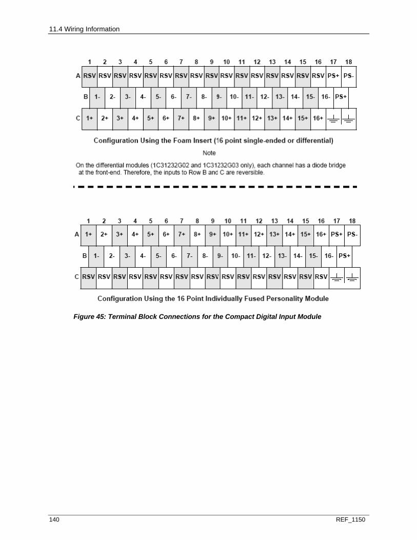
11.4 Wiring Information
140 REF_1150
Figure 45: Terminal Block Connections for the Compact Digital Input Module

11.4 Wiring Information
REF_1150 141
11.4.2 FIELD WIRING CONSIDERATIONS FOR THE SINGLE-ENDED COMPACT DIGITAL INPUT FRONT END
The following maximum resistances of the cable and the interfaced device apply:
24/48VDC - 175 KW 24 VAC - 50 KW 125 VDC - 225 KW 125 VAC - 50 KW
CAUTION! For CE Mark certified systems: Any base unit that contains a 125VAC/DC Compact Digital Input Electronics module (1C31232G03) with foam insert (1C31238H01) and interfaces to hazardous voltage (>30 V RMS, 42.4 V peak, or 60 VDC) must include a hazardous voltage warning label (1B30025H01) on that base unit.
Any base unit that contains a 125VAC/DC Compact Digital Input Electronics module (1C31232G03) with the individually fused Personality Module (5X00034G01) and interfaces to hazardous voltage (>30 V RMS, 42.4 V peak, or 60 VDC) must include a hazardous voltage warning label (1B30025H01) on ALL base units on the branch.
This label must be placed in a visible location on the base unit, preferably above the spare fuse location. The project drawings must indicate this.
OPTO-ISOLATOR
A1B1C1
FIELDCONTACT
CHANNEL 1currentlimiter
OPTO-ISOLATOR
currentlimiter
A2B2C2
FIELDCONTACT
CHANNEL 2
CHANNELS 3 - 16
WE
TTING
VO
LTAG
E +
WE
TTING
VO
LTAG
E -
(TO OTHER BASE UNITS)
(TO OTHER BASE UNITS)
FUSE
OPTO-ISOLATOR
currentlimiter
CHANNEL 1
CHANNEL 2
BLOWN FUSE MONITOR
AU
XILIA
RY
AU
XILIA
RY

11.4 Wiring Information
142 REF_1150
Figure 46: Single-Ended Compact Digital Input Front End
11.4.3 FIELD WIRING CONSIDERATIONS FOR THE DIFFERENTIAL COMPACT DIGITAL INPUT FRONT END
The following maximum resistances of the cable and the interfaced device apply:
24/48VDC - 175 KW 24 VAC - 50 KW 125 VDC - 225 KW 125 VAC - 50 KW
CAUTION! (For CE Mark Certified Systems): Any base unit that contains a 125VAC/DC Compact Digital Input Electronics module (1C31232G03) with foam insert (1C31238H01) and interfaces to hazardous voltage (>30 V RMS, 42.4 V peak, or 60 VDC) must include a hazardous voltage warning label (1B30025H01) on that base unit.
Any base unit that contains a 125VAC/DC Compact Digital Input Electronics module (1C31232G03) with the individually fused Personality Module (5X00034G01) and interfaces to hazardous voltage (>30 V RMS, 42.4 V peak, or 60 VDC) must include a hazardous voltage warning label (1B30025H01) on ALL base units on the branch.
This label must be placed in a visible location on the base unit, preferably above the spare fuse location. The project drawings must indicate this.
OPTO-ISOLATOR
A1B1C1FIELD
CONTACT
CHANNEL 1 currentlimiter
OPTO-ISOLATOR
currentlimiter
A2B2C2FIELD
CONTACT
CHANNEL 2
CHANNELS 3 - 16
(TO OTHER BASE UNITS)
CHANNEL 1
CHANNEL 2
DC
DC
*
*
* Auxiliary power supply may be AC or DC. If a DC supply is used, the polarity can beopposite of what is shown.
Figure 47: Differential Compact Digital Input Front End
11.4 Wiring Information
REF_1150 143
11.4.4 FIELD WIRING CONSIDERATIONS FOR THE 16 INDIVIDUALLY FUSED COMPACT DIGITAL INPUT FRONT END
The following maximum resistances of the cable and the interfaced device apply:
24/48VDC - 175 KW 24 VAC - 50 KW 125 VDC - 225 KW 125 VAC - 50 KW
CAUTION! (For CE Mark Certified Systems): Any base unit that contains a 125VAC/DC Compact Digital Input Electronics module (1C31232G03) with foam insert (1C31238H01) and interfaces to hazardous voltage (>30 V RMS, 42.4 V peak, or 60 VDC) must include a hazardous voltage warning label (1B30025H01) on that base unit.
Any base unit that contains a 125VAC/DC Compact Digital Input Electronics module (1C31232G03) with the individually fused Personality Module (5X00034G01) and interfaces to hazardous voltage (>30 V RMS, 42.4 V peak, or 60 VDC) must include a hazardous voltage warning label (1B30025H01) on ALL base units on the branch.
This label must be placed in a visible location on the base unit, preferably above the spare fuse location. The project drawings must indicate this.

11.4 Wiring Information
144 REF_1150
Figure 48: 16 Individually Fused Compact Digital Inputs Front End

11.4 Wiring Information
REF_1150 145
11.4.5 NON-CE MARK CERTIFIED SYSTEM
Field
Single-Ended Digital Voltage Inputs
Contacts16
PS+
PS-
1-
1+
16-
16+
PowerMonitor
Rtn
Electronics Module
SurgeProtection
AuxiliaryVoltageSupply
0.5A
Field
Differential Digital Voltage Inputs
Devices
1-
1+
16-
16+
AuxiliaryVoltageSupplies
16
Field
16 Individually Fused Digital Voltage Inputs
Contacts16
PS+
PS-
1+
1-
AuxiliaryVoltageSupply
0.5A
0.5A
16+
16-
Electronics Module
Electronics ModulePersonality Module
Channel1
Channel1
Channel1
Channel16
Channel16
Channel16
* Auxiliary power supply may be AC or DC. It a DC supply is used, the polarity can be opposite of what is shown.
*
*
Figure 49: Field Connections for the Compact Digital Input Module (Non-CE Mark)

11.4 Wiring Information
146 REF_1150
11.4.6 CE MARK CERTIFIED SYSTEM
Field
Single-Ended Digital Voltage Inputs
Contacts16
PS+
PS-
1-
1+
16-
16+
PowerMonitor
Rtn
Electronics Module
SurgeProtection
AuxiliaryVoltageSupply
0.5A
Field
Differential Digital Voltage Inputs
Devices
1-
1+
16-
16+
AuxiliaryVoltageSupplies
16
Field
16 Individually Fused Digital Voltage Inputs
Contacts16
PS+
PS-
1+
1-
AuxiliaryVoltageSupply
0.5A
0.5A
16+
16-
Electronics Module
Electronics ModulePersonality Module
Channel1
Channel1
Channel1
Channel16
Channel16
Channel16
* Auxiliary power supply may be AC or DC. It a DC supply is used, the polarity can be opposite of what is shown.
*
*
All field wiring
grounded at the entry
(refer to the
(each pair separately or all together) must be braid shielded and
point of the cabinet using the recommended hardwareapplicable "Cable Guidelines"information for your system).
Figure 50: Field Connections for the Compact Digital Input Module (CE Mark)

11.5 Address Location Information
REF_1150 147
11.5 ADDRESS LOCATION INFORMATION
11.5.1 CONFIGURATION AND STATUS REGISTER
Word address 13 (D in Hex) is used to configure the module and provide status information to the Controller. The status register can be read by using the Point Information window at an Operator Station (see the Bit Pattern field on the Hardware tab). (See the Ovation Operator Station User Guide.)
Digital (and Compact Digital) Input Configuration/Status (Address 13 or D in Hex)
BI T DAT A DE S C R I P T I O N - CO NF I G U R AT I O N RE GI S T E R (WRI T E)
DAT A DE S C R I P T I O N - ST AT U S REGI S TER (RE AD)
0 Configure Module
(1 = configure; 0 = unconfigure, causing an attention status)
Module Configured
(1 = configured; 0 = unconfigured)
1 Force Error
(1 = force an attention status to be read by Controller; 0 = no forced error)
Forced error
(1 = forced error set by Controller; 0 = no forced error)
2 Not defined Not defined
3 Not defined Not defined
4 Not defined Not defined
5 Not defined Not defined
6 Blown fuse enable 1
(1 = enable blown fuse detection; 0 = disable blown fuse detection)
Blown fuse enable
(1 = blown fuse detection is enabled; 0 = blown fuse detection is disabled)
7 Not defined Blown fuse
(1 = fuse blown or auxiliary voltage not present; 0 = fuse OK and auxiliary voltage present)
8 Not defined Reserved
9 Reserved Reserved
10 Not defined Reserved
11 Not defined Not defined
12 Not defined Not defined
13 Not defined Not defined
14 Not defined Not defined
15 Not defined Not defined
1 Blown Fuse Enable should always be set to “0” on the differential modules (1C31232G02 and 1C31232G03).

11.6 Diagnostic LEDs
148 REF_1150
Bit definitions for this register are encoded as shown in the table above and described below:
Bit 0: After the Compact Digital Input Module power is cycled, this bit is “0.” A “1” must be written to this bit. If the module is not configured in this manner, an attention status will be sent to the Controller upon an attempt to read the point data.
Bit 1: This bit is “0” after the Compact Digital Input Module power is cycled. If the Controller sets this bit, an attention status is issued.
Bits 2-5, 11-15: These bits are not defined in the Configuration register and will be read as high in the Status register.
Bit 6: The Blown Fuse Enable bit is “0” after the Digital Input module power is cycled. This bit must be set by the Controller for Compact Digital Input Modules, using the single-ended personality module, to detect a blown auxiliary power supply fuse when it reads the Status Register. Blown Fuse Enable should always be set to “0”on the differential modules (1C31232G02 and 1C31232G03). The bit may be read back through the Module Status Register.
Bit 7: This bit is set in the Status Register only if the Blown Fuse Enable bit (6) is set and the single-ended on-board auxiliary supply fuse has blown or the auxiliary voltage is not present. This bit is not defined in the Configuration Register.
Bit 8, 10: These bits are reserved in the Status Register. These bits are not defined in the Configuration Register.
Bit 9: This bit is reserved.
11.6 DIAGNOSTIC LEDS
The following table lists the module’s LEDs and describes what they mean when lit.
Compact Digital Input Diagnostic LEDs
LED DE S C RI P T I O N
P (Green) Power OK LED. Lit when the +5V power is OK.
C (Green) Communications OK LED. Lit when the Controller is communicating with the Compact Digital Input module.
E (Red) External Fault LED. Lit when the Blown Fuse bit (Bit 7) of the Status Register (see page 133) is set. This indicates the field supply fuse is blown or the auxiliary power supply is not present. This LED should never light if the Compact Digital Input module is installed since the Blown Fuse Enable bit (Bit 6) of the Status Register should be set to the inactive state by the Controller.
I (Red) Internal Fault LED. Lit whenever the Force Error bit (Bit 1) of the Configuration Register (see page 133) is active or when a timeout of the watchdog timer occurs when the Controller stops communicating with the module.
CH1 - CH 16 (Green) Point Status LED. Lit when the input voltage of the LED’s corresponding channel is greater than the channel’s minimum On Input Voltage.
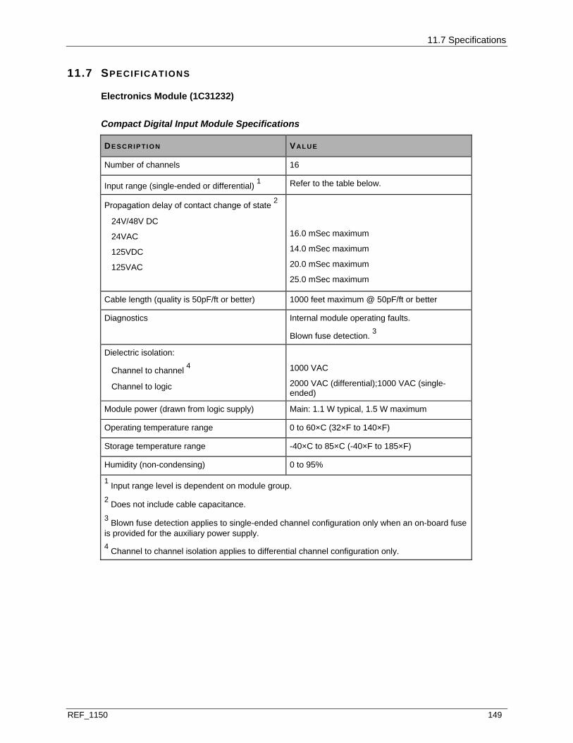
11.7 Specifications
REF_1150 149
11.7 SPECIFICATIONS
Electronics Module (1C31232)
Compact Digital Input Module Specifications
DE S C RI P T I O N VAL U E
Number of channels 16
Input range (single-ended or differential) 1 Refer to the table below.
Propagation delay of contact change of state 2
24V/48V DC
24VAC
125VDC
125VAC
16.0 mSec maximum
14.0 mSec maximum
20.0 mSec maximum
25.0 mSec maximum
Cable length (quality is 50pF/ft or better) 1000 feet maximum @ 50pF/ft or better
Diagnostics Internal module operating faults.
Blown fuse detection. 3
Dielectric isolation:
Channel to channel 4
Channel to logic
1000 VAC
2000 VAC (differential);1000 VAC (single-ended)
Module power (drawn from logic supply) Main: 1.1 W typical, 1.5 W maximum
Operating temperature range 0 to 60×C (32×F to 140×F)
Storage temperature range -40×C to 85×C (-40×F to 185×F)
Humidity (non-condensing) 0 to 95%
1 Input range level is dependent on module group. 2 Does not include cable capacitance. 3 Blown fuse detection applies to single-ended channel configuration only when an on-board fuse is provided for the auxiliary power supply. 4 Channel to channel isolation applies to differential channel configuration only.
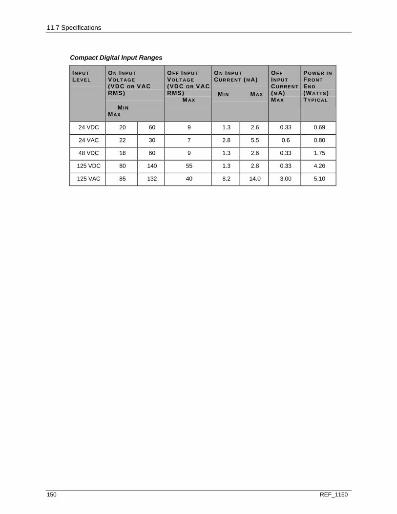
11.7 Specifications
150 REF_1150
Compact Digital Input Ranges
IN P U T LEV E L
ON INP U T VO L T AG E (VDC O R VAC RMS)
MI N MAX
OF F INP U T VO L T AG E (VDC O R VACRMS) MAX
ON INP U T CU R R E N T (MA)
MI N MAX
OF F IN P U T CU R R E N T (M A) MAX
PO WE R I N FR O NT EN D (WAT T S) TYPI C AL
24 VDC 20 60 9 1.3 2.6 0.33 0.69
24 VAC 22 30 7 2.8 5.5 0.6 0.80
48 VDC 18 60 9 1.3 2.6 0.33 1.75
125 VDC 80 140 55 1.3 2.8 0.33 4.26
125 VAC 85 132 40 8.2 14.0 3.00 5.10

REF_1150 151
IN THIS SECTION
Description ......................................................................................................................151 Module Group Information ..............................................................................................151 Module Specific Information............................................................................................153 Wiring Information ...........................................................................................................164 Address Location Information .........................................................................................173 Diagnostic LEDs..............................................................................................................175 Specifications ..................................................................................................................175
12.1 DESCRIPTION
The Ovation digital output module provides a means to switch up to 60 VDC at moderate currents (for example, relay coils and lamps). The digital output module contains 16 current sinking transistor outputs capable of switching 60 VDC loads at up to 500mA.
The digital output module provides configurable communication timeout periods and LEDs to indicate the status of each output.
The Digital Output Module is applicable for CE Mark Certified Systems.
Note: I/O Module General Information (see page 15) contains environmental, installation, wiring, and fuse information for I/O modules.
12.2 MODULE GROUP INFORMATION
12.2.1 ELECTRONICS MODULE (EMOD)
There is one Electronics module group for the Digital Output Module:
1C31122G01 provides for switching 60 VDC loads.
S E C T I O N 1 2
DIGITAL OUTPUT MODULE

12.2 Module Group Information
152 REF_1150
12.2.2 PERSONALITY MODULES (PMODS)
There are three Personality module groups for the Digital Output Module:
1C31125G01 is used to interface the digital output module to the field through the terminal blocks.
1C31125G02 is used to interface the digital output module to the relay modules when power is supplied locally (from the I/O backplane auxiliary power supply). It can also be used to interface the digital output module to the field through the terminal blocks.
1C31125G03 is used to interface the digital output module to the relay modules when power is supplied remotely (from the relay modules). It can also can be used to interface the digital output module to the field through the terminal blocks.
CAUTION! When 1C31125G03 is used, the returns for the remote power supply and the local power supply are connected together. Therefore, to avoid problems with differences in earth ground potentials, ensure that the power supply return lines are earth grounded at only ONE point.
12.2.3 SUBSYSTEMS, DIGITAL OUTPUT
Digital Output Subsystems 1
DE S C RI P T I O N CH AN N E L S EL E C T RO NI C MO D U LE O R PAN E L KI T
PE R S O N AL I T Y MO D U LE
0-60 VDC Single ended Direct 16 1C31122G01 1C31125G01
Relay Panel Interface:
Local Power Supply
Field Power Supply
16
16
1C31122G01
1C31122G01
1C31125G02
1C31125G03
Relay Panels:
Solid State Relay Panel (AC)
Solid State Relay Panel (DC)
G2R Relay Panel
(Low Power Electro-mechanical)
KU Relay Panel 2
(High Power Electro-mechanical)
16
16
16
16
5A22410G01
5A22410G02
5A22411G01
5A22412G01, G02, G03
1 All configurations are CE Mark certified, except AC/DC Solid State Relay Panels. 2 Two panels (8 relays each) are included in the KU Relay Panel kit 5A22412G01, G02, and G03.

12.3 Module Specific Information
REF_1150 153
12.3 MODULE SPECIFIC INFORMATION
12.3.1 EXTERNAL POWER SUPPLIES
The Digital Output module may obtain voltage from the internal auxiliary power supply (backplane) or from an external power supply.
If an external power supply is used, Using an External Power Supply (see page 539) contains steps to be undertaken before connecting the external power supply to the Digital Output module base unit terminal block. The external power supply DC output voltage level depends on the Digital Output module application.
12.3.2 RELAY PANELS
Relay panels are used to switch high currents and high voltages as required by various field devices. The Digital Output module interfaces to the relay modules through Groups 2 and 3 of the Personality modules and a standard cable.
The following table provides information about the three standard relay modules.
Relay Contact Ratings must be adhered to when utilizing the Digital Output Relay Panel Assemblies. The application must include external current limiting protection for the Digital Output Relay Panel Assemblies.
Digital Output Relay Panels
RE L AY MO D UL E CE MAR K
SI ZE NUM BE R O F CH AN N E L S
CO N T AC TTYP E
CO N T ACT RAT I N G
IN P U T PO WE R
CO N N E CT CAB L E
5A22410G01
Solid State
No 35.86 cm L
(14.12 in)
7.75 cm W
(3.05 in)
10.46 cm H
(4.12 in)
16 Solid State
(1 normally open)
3.5 amps @250 VAC at 25 °C
1.65 amps @250 VAC at 60 °C
246mA typ
310mA max
@26.4V
5A26148
5A22410G02
Solid State
No 35.86 cm L
(14.12 in)
7.75 cm W
(3.05 in)
10.46 cm H
(4.12 in)
16 Solid State
(1 normally open)
1.0 amps @200 VDC at 60 °C
246mA typ
310mA max
@26.4V
5A26148

12.3 Module Specific Information
154 REF_1150
RE L AY MO D UL E CE MAR K
SI ZE NUM BE R O F CH AN N E L S
CO N T AC TTYP E
CO N T ACT RAT I N G
IN P U T PO WE R
CO N N E CT CAB L E
5A22411G01
G2R Style
(Low Power Electromechanical)
Yes 45.09 cm L
(17.75 in)
7.75 cm W
(3.05 in)
6.05 cm H
(2.38 in)
16 Mechanical
(1 Form C)
10 amps @250 VAC
10 amps @30 VDC
453mA typ
610mA max
@26.4V
5A26148
5A22412G01 1
KUEP Style
(High Power Electromechanical)
Contains two
5A22412H01 panels and 16 4960A71H16 relays.
Yes
49.5 cm L
(19.5 in)
7.75 cm W
(3.05 in)
9.53 cm H
(3.75 in)
16
(using two panels)
Mechanical
(2 Form C)
10 amps @250 VAC
3 amps @150 VDC
1.32A typ
1.8A max
@26.4V
(for 2 relay panels) 2
5A26149
5A22412G02 1
KUEP Style
(High Power Electro-mechanical)
Contains two
5A22412H01 panels and 16 4960A71H05 relays.
Yes
49.5 cm L
(19.5 in)
7.75 cm W
(3.05 in)
9.53 cm H
(3.75 in)
16
(using two panels)
Mechanical
(Form X)
10 amps @250 VAC
10 amps @150 VDC
940mA typ
1.27A max
@26.4V
(for 2 relay panels) 2
5A26149
5A22412G03 1
KUEP Style
(High Power Electromechanical)
Contains two
5A22412H01 panels and up to 16 project specific relays.
Yes
49.5 cm L
(19.5 in)
7.75 cm W
(3.05 in)
9.53 cm H
(3.75 in)
16
(using two panels)
Project Specific
Project Specific
Project Specific
5A26149
1 Two panels required for 16 outputs. 2 If one panel is used, half the power is needed.

12.3 Module Specific Information
REF_1150 155
Solid State Relay Module for DIN Rail Layout (5A22410H01/5A22410H02) (Non CE Mark Certified Systems)
R16
R1
R15
R14
R13
R12
R11
R10
R9
R8
R7
R6
R5
R4
R3
R2
2
1N
C N
0 C
2
12
1
2
12
1
2
12
1
2
12
1
2
12
1
2
12
1
2
12
1
2
1
24 VDC Power Fuse24 VDC Power Connector
LED for 24VDCPower Failure
25 Pin "D"Connector
Relay
Retainer Screw
Contact Fuse
Contact StatusLED
Field WiringTerminalBlocks
24 VDC Alarm Relay
Figure 51: Solid State Relay Module for DIN Rail Layout (5A22410H01/5A22410H02)

12.3 Module Specific Information
156 REF_1150
Solid State Relay Module for DIN Rail Layout (5A22410H01/5A22410H02) (Non CE Mark Certified Systems)
R16
R1
R15
R14
R13
R12
R11
R10
R9
R8
R7
R6
R5
R4
R3
R2
2
1N
C N
0 C
2
12
1
2
12
1
2
12
1
2
12
1
2
12
1
2
12
1
2
12
1
2
1
24 VDC Power Fuse24 VDC Power Connector
LED for 24VDCPower Failure
25 Pin "D"Connector
Relay
Retainer Screw
Contact Fuse
Contact StatusLED
Field WiringTerminalBlocks
24 VDC Alarm Relay
Figure 52: Solid State Relay Module for DIN Rail Layout (5A22410H01/5A22410H02)
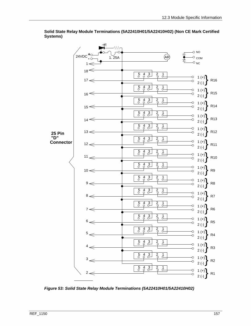
12.3 Module Specific Information
REF_1150 157
Solid State Relay Module Terminations (5A22410H01/5A22410H02) (Non CE Mark Certified Systems)
5 4 3 2 11 (+)2 (-)} R16
5 4 3 2 11 (+)2 (-)} R1
5 4 3 2 11 (+)2 (-)} R15
5 4 3 2 11 (+)2 (-)} R14
5 4 3 2 11 (+)2 (-)} R13
5 4 3 2 11 (+)2 (-)} R12
5 4 3 2 11 (+)2 (-)} R11
5 4 3 2 11 (+)2 (-)} R10
5 4 3 2 11 (+)2 (-)} R9
5 4 3 2 11 (+)2 (-)} R8
5 4 3 2 11 (+)2 (-)} R7
5 4 3 2 11 (+)2 (-)} R6
5 4 3 2 11 (+)2 (-)} R5
5 4 3 2 11 (+)2 (-)} R4
5 4 3 2 11 (+)2 (-)} R3
5 4 3 2 11 (+)2 (-)} R2
ARNO
COM
NC
1. 25A24VDC
1
18
17
16
15
14
13
12
11
10
9
8
7
6
5
4
3
2
+-
25 Pin"D"Connector
Figure 53: Solid State Relay Module Terminations (5A22410H01/5A22410H02)

12.3 Module Specific Information
158 REF_1150
G2R Style Relay Module for DIN Rail Layout (5A22411H01)
R16
R1
R15
R14
R13
R12
R11
R10
R9
R8
R7
R6
R5
R4
R3
R2
NC
N0
C24 VDC Power Fuse24 VDC Power Connector
LED for 24VDCPower Failure
25 Pin "D"Connector
Relay
Relay StatusLED
24 VDC Alarm Relay
Field Wiring
Contact Diagram
Relay RetainerClip
NC
N0
CN
C N
0 C
NC
N0
CN
C N
0 C
NC
N0
CN
C N
0 C
NC
N0
CN
C N
0 C
NC
N0
CN
C N
0 C
NC
N0
CN
C N
0 C
NC
N0
CN
C N
0 C
NC
N0
CN
C N
0 C
Terminal Blocks
Figure 54: G2R Style Relay Module for DIN Rail Layout (5A22411H01)
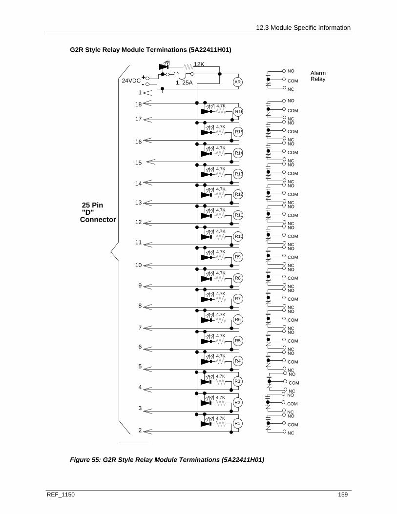
12.3 Module Specific Information
REF_1150 159
G2R Style Relay Module Terminations (5A22411H01)
AR
NO
COM
NC1. 25A24VDC
1
18
17
16
15
14
13
12
11
10
9
8
7
6
5
4
3
2
+-
25 Pin"D"Connector
4.7K
Alarm Relay
R16
12K
4.7KR15
4.7KR14
4.7KR12
4.7KR13
4.7KR11
4.7KR10
4.7KR8
4.7KR9
4.7KR7
4.7KR6
4.7KR5
4.7KR4
4.7KR2
4.7KR3
4.7KR1
NO
COM
NCNO
COM
NCNO
COM
NCNO
COM
NCNO
COM
NCNO
COM
NCNO
COM
NC
NO
COM
NC
NO
COM
NCNO
COM
NCNO
COM
NCNO
COM
NCNO
COM
NC
NO
COM
NC
NO
COM
NC
NO
COM
NC
Figure 55: G2R Style Relay Module Terminations (5A22411H01)
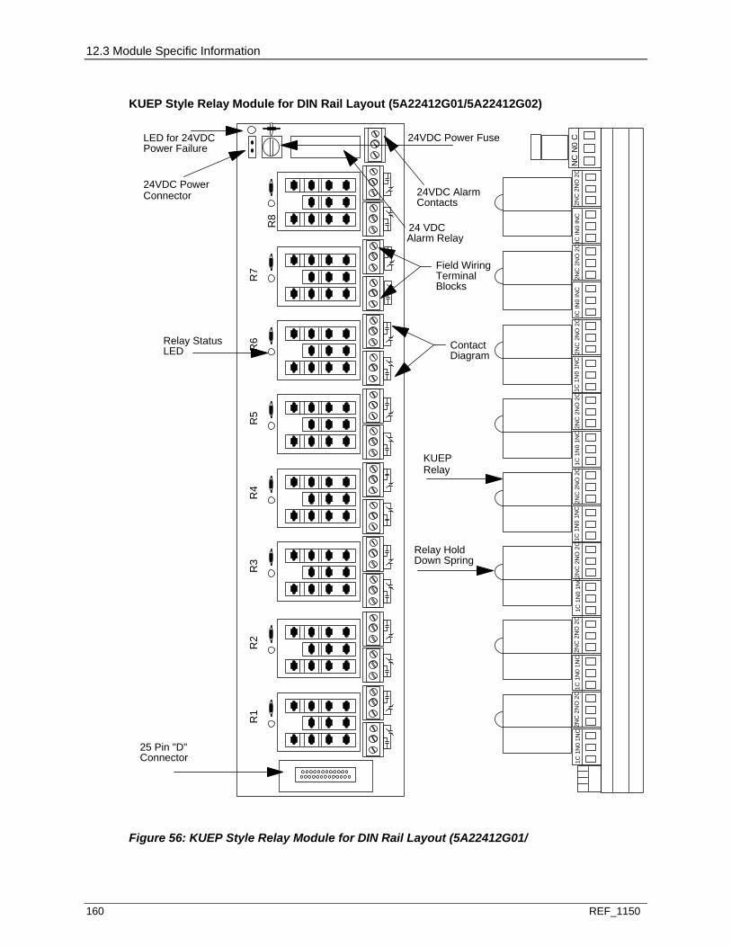
12.3 Module Specific Information
160 REF_1150
KUEP Style Relay Module for DIN Rail Layout (5A22412G01/5A22412G02)
R8
R7
R6
NC
N0
C24VDC Power Fuse
24VDC Power Connector
LED for 24VDCPower Failure
25 Pin "D"Connector
Relay StatusLED
24 VDC Alarm Relay
Contact
1C 1
N0
1NC
24VDC AlarmContacts
Field WiringTerminal
R5
R4
R3
R2
R1
Blocks
Diagram
KUEPRelay
Relay HoldDown Spring
1C 1
N0
1NC
1C 1
N0
1NC
1C 1
N0
1NC
1C 1
N0
1NC
1C 1
N0
1NC
IC IN
0 IN
CIC
IN0
INC
2NC
2N
O 2
C2N
C 2
NO
2C
2NC
2N
O 2
C2N
C 2
NO
2C
2NC
2N
O 2
C2N
C 2
NO
2C
2NC
2N
O 2
C2N
C 2
NO
2C
Figure 56: KUEP Style Relay Module for DIN Rail Layout (5A22412G01/

12.3 Module Specific Information
REF_1150 161
KUEP (2 Form C) Style Relay Module Terminations (5A22412G01)
AR
NO
COM
NCF11 2A24VDC
1
18
9
8
7
6
5
4
3
2
+-
25 Pin"D"Connector
4.7KR8
12K
4.7KR7
4.7KR6
4.7KR5
4.7KR4
4.7KR3
4.7KR2
4.7KR1
2NO
2C
2NC1NO
1C
1NC2NO
2C
2NC1NO
1C
1NC2NO
2C
2NC1NO
1C
1NC2NO
2C
2NC
1NO
1C
1NC
1NO
1C
1NC2NO
2C
2NC1NO
1C
1NC2NO
2C
2NC1NO
1C
1NC
2NO
2C
2NC
2NO
2C
2NC
1NO
1C
1NC
Note:Only the firsteight relays ofthe first relaypanel are shown.
Figure 57: KUEP (2 Form C) Style Relay Module Terminations (5A22412G01)

12.3 Module Specific Information
162 REF_1150
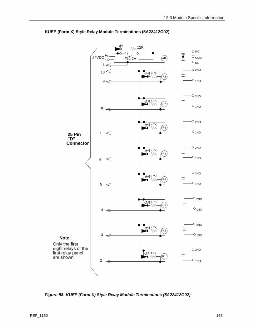
12.3 Module Specific Information
REF_1150 163
KUEP (Form X) Style Relay Module Terminations (5A22412G02)
AR
NO
COM
NCF11 2A24VDC
1
18
9
8
7
6
5
4
3
2
+-
25 Pin"D"Connector
4.7KR8
12K
4.7KR7
4.7KR6
4.7KR5
4.7KR4
4.7KR3
4.7KR2
4.7KR1
2NO
1NO
Note:Only the firsteight relays of thefirst relay panel
2NO
1NO
2NO
1NO
2NO
1NO
2NO
1NO
2NO
1NO
2NO
1NO
2NO
1NO
are shown.
Figure 58: KUEP (Form X) Style Relay Module Terminations (5A22412G02)
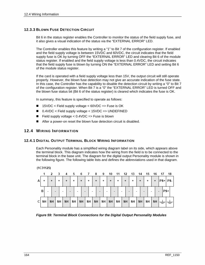
12.4 Wiring Information
164 REF_1150
12.3.3 BLOWN FUSE DETECTION CIRCUIT
Bit 6 in the status register enables the Controller to monitor the status of the field supply fuse, and it also gives a visual indication of the status via the “EXTERNAL ERROR” LED.
The Controller enables this feature by writing a “1” to Bit 7 of the configuration register. If enabled and the field supply voltage is between 15VDC and 60VDC, the circuit indicates that the field supply fuse is OK by turning OFF the “EXTERNAL ERROR” LED and clearing Bit 6 of the module status register. If enabled and the field supply voltage is less than 0.4VDC, the circuit indicates that the field supply fuse is blown by turning ON the “EXTERNAL ERROR” LED and setting Bit 6 of the module status register.
If the card is operated with a field supply voltage less than 15V, the output circuit will still operate properly. However, the blown fuse detection may not give an accurate indication of the fuse state. In this case, the Controller has the capability to disable the detection circuit by writing a “0” to Bit 7 of the configuration register. When Bit 7 is a “0” the “EXTERNAL ERROR” LED is turned OFF and the blown fuse status bit (Bit 6 of the status register) is cleared which indicates the fuse is OK.
In summary, this feature is specified to operate as follows:
15VDC < Field supply voltage < 60VDC => Fuse is OK 0.4VDC < Field supply voltage < 15VDC => UNDEFINED Field supply voltage < 0.4VDC => Fuse is blown After a power-on reset the blown fuse detection circuit is disabled.
12.4 WIRING INFORMATION
12.4.1 DIGITAL OUTPUT TERMINAL BLOCK WIRING INFORMATION
Each Personality module has a simplified wiring diagram label on its side, which appears above the terminal block. This diagram indicates how the wiring from the field is to be connected to the terminal block in the base unit. The diagram for the digital output Personality module is shown in the following figure. The following table lists and defines the abbreviations used in that diagram.
Figure 59: Terminal Block Connections for the Digital Output Personality Modules
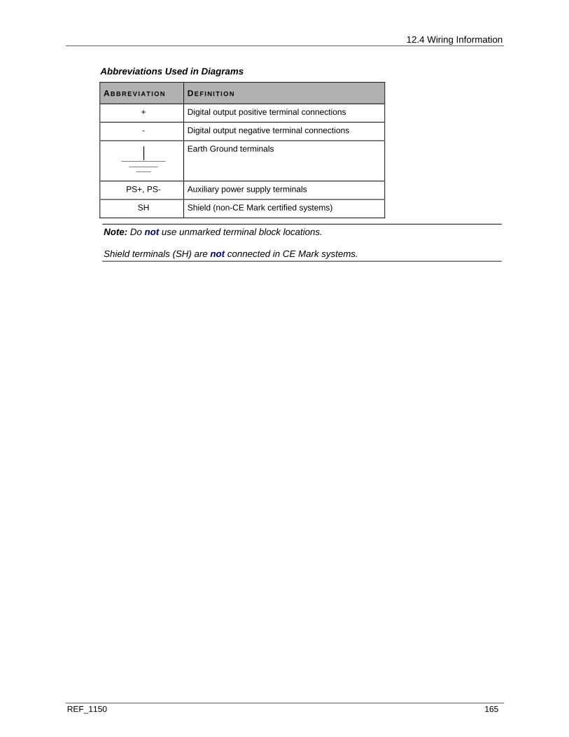
12.4 Wiring Information
REF_1150 165
Abbreviations Used in Diagrams
AB B R E V I AT I ON DE FI N I T I O N
+ Digital output positive terminal connections
- Digital output negative terminal connections
Earth Ground terminals
PS+, PS- Auxiliary power supply terminals
SH Shield (non-CE Mark certified systems)
Note: Do not use unmarked terminal block locations.
Shield terminals (SH) are not connected in CE Mark systems.

12.4 Wiring Information
166 REF_1150
12.4.2 DIGITAL OUTPUT FIELD CONNECTION WIRING DIAGRAMS
Electronics Module Personality Module
Load
1.25 APS+
+
-
PS-
SH
V (Local)
+-
Notes1. V (Local) is the I/O backplane auxiliary power supply.2. Shielded cables are required for IEC 801-5 compliance.
Group 1
1 of 16
1 of 16
Figure 60: Field Connection for the Digital Output Personality Module (Group 1) (Non-CE Mark Certified Systems)
Electronics Module Personality Module
Load
1.25 APS+
+
-
PS-
V (Local)
+-
Notes1. V (Local) is the I/O backplane auxiliary power supply.2. Shielded cables are required for IEC 801-5 compliance.
Group 1
1 of 16
1 of 16
3. All field wiring must be braid shielded and grounded at the entry point of the cabinet using therecommended hardware (see the appropriate "Cable Guidelines" information for your system).
Seenote 3
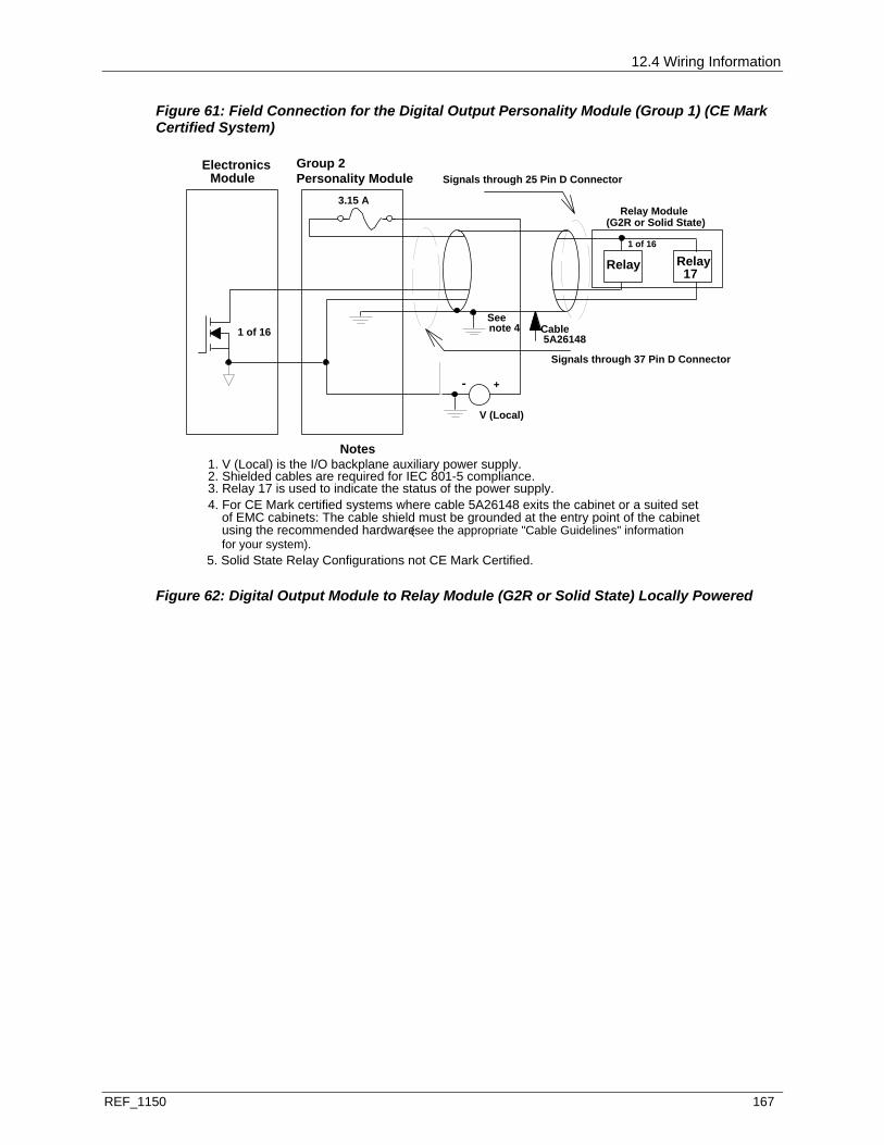
12.4 Wiring Information
REF_1150 167
Figure 61: Field Connection for the Digital Output Personality Module (Group 1) (CE Mark Certified System)
ElectronicsPersonality Module
3.15 A
V (Local)
+-
Notes1. V (Local) is the I/O backplane auxiliary power supply.2. Shielded cables are required for IEC 801-5 compliance.
Group 2
1 of 16
1 of 16
3. Relay 17 is used to indicate the status of the power supply.
Relay17
Relay
Relay Module(G2R or Solid State)
Signals through 37 Pin D Connector
Signals through 25 Pin D Connector
Cable 5A26148
4. For CE Mark certified systems where cable 5A26148 exits the cabinet or a suited setof EMC cabinets: The cable shield must be grounded at the entry point of the cabinet using the recommended hardware (see the appropriate "Cable Guidelines" information
Seenote 4
5. Solid State Relay Configurations not CE Mark Certified.
Module
for your system).
Figure 62: Digital Output Module to Relay Module (G2R or Solid State) Locally Powered
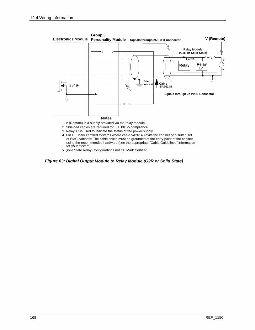
12.4 Wiring Information
168 REF_1150
Electronics Module Personality Module
Notes
2. Shielded cables are required for IEC 801-5 compliance.
Group 3
1 of 16
1 of 16
3. Relay 17 is used to indicate the status of the power supply.
Relay17
Relay
Relay Module(G2R or Solid State)
Signals through 37 Pin D Connector
1. V (Remote) is a supply provided via the relay module.
+
-
V (Remote)Signals through 25 Pin D Connector
Cable 5A26148
4. For CE Mark certified systems where cable 5A26148 exits the cabinet or a suited setof EMC cabinets: The cable shield must be grounded at the entry point of the cabinetusing the recommended hardware (see the appropriate "Cable Guidelines" information
Seenote 4
5. Solid State Relay Configurations not CE Mark Certified..for your system).
Figure 63: Digital Output Module to Relay Module (G2R or Solid State)

12.4 Wiring Information
REF_1150 169
Electronics Module Personality Module 3.15 A
Notes
1. V (Local) is the I/O backplane auxiliary power supply.2. Shielded cables are required for IEC 801-5 compliance.
Group 2
1 of 8
1 of 8
3. Relay 9 is used to indicate the status of the power supply.
Relay9
Relay
Relay Module(KUEP Style)
V (Local)
+-
1 of 8
1 of 8
Relay9
Relay
Relay Module(KUEP Style)
Signals through 37 Pin D Connector
Signals through 25 Pin D Connector
Signals through 25 Pin D Connector
Cable 5A26149
Cable 5A26149
Seenote 4
4. For CE Mark certified systems where cable 5A26149 exits the cabinet or a suited setof EMC cabinets: The cable shield must be grounded at the entry point of the cabinetusing the recommended hardware (see the appropriate "Cable Guidelines" information
Seenote 4
for your system).
Figure 64: Digital Output Module to Relay Module (KUEP Style) Locally Powered (Non-CE and CE Mark)
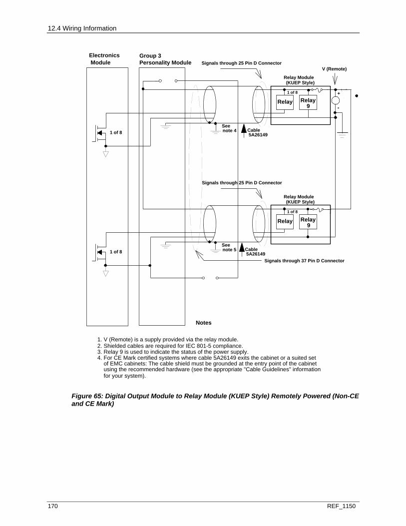
12.4 Wiring Information
170 REF_1150
ElectronicsPersonality Module
Notes
2. Shielded cables are required for IEC 801-5 compliance.
Group 3
1 of 8
1 of 8
3. Relay 9 is used to indicate the status of the power supply.
Relay9
Relay
Relay Module(KUEP Style)
1 of 8
1 of 8
Relay9
Relay
Relay Module(KUEP Style)
Signals through 37 Pin D Connector
1. V (Remote) is a supply provided via the relay module.
Module +
-
V (Remote)Signals through 25 Pin D Connector
Signals through 25 Pin D Connector
Cable 5A26149
Cable 5A26149
Seenote 4
Seenote 5
4. For CE Mark certified systems where cable 5A26149 exits the cabinet or a suited setof EMC cabinets: The cable shield must be grounded at the entry point of the cabinetusing the recommended hardware (see the appropriate "Cable Guidelines" informationfor your system).
Figure 65: Digital Output Module to Relay Module (KUEP Style) Remotely Powered (Non-CE and CE Mark)
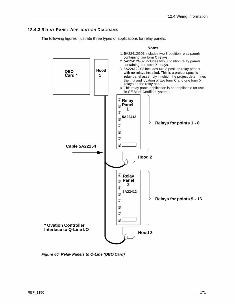
12.4 Wiring Information
REF_1150 171
12.4.3 RELAY PANEL APPLICATION DIAGRAMS
The following figures illustrate three types of applications for relay panels.
QBOCard *
Hood 1
RelayPanel
1
RelayPanel
2
Hood 2
Hood 3
Relays for points 1 - 8
Relays for points 9 - 16
Cable 5A22254
* Ovation Controller Interface to Q-Line I/O
R1
R8
R2
R3
R4
R5
R6
R7
R1
R8
R2
R3
R4
R5
R6
R7
Hood1
1. 5A22412G01 includes two 8 position relay panelscontaining two form C relays.
2. 5A22412G02 includes two 8 position relay panels
3. 5A22412G03 includes two 8 position relay panelscontaining one form X relays.
with no relays installed. This is a project specific relay panel assembly in which the project determinesthe mix and location of two form C and one form Xrelays on the relay panel.
4. This relay panel application is not applicable for usein CE Mark Certified systems.
5A22412.
5A22412.
Notes
Figure 66: Relay Panels to Q-Line (QBO Card)
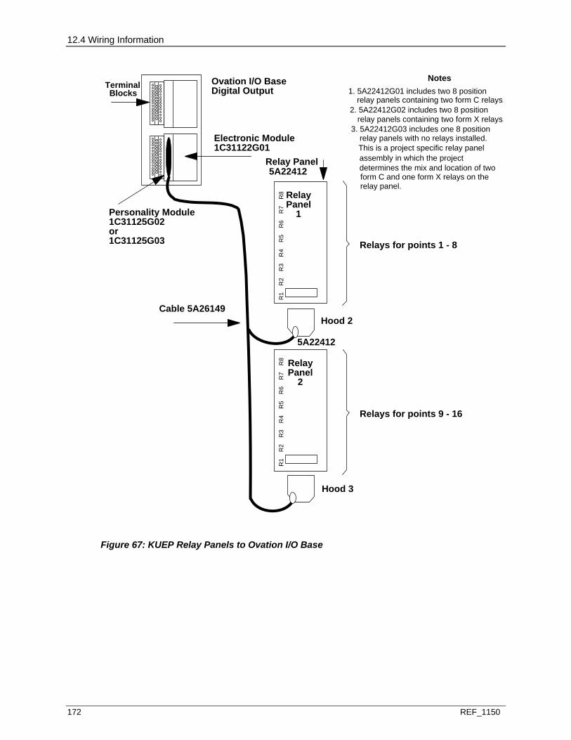
12.4 Wiring Information
172 REF_1150
RelayPanel
1
RelayPanel
2
Hood 2
Hood 3
Relays for points 1 - 8
Relays for points 9 - 16
Electronic Module1C31122G01
Personality Module1C31125G02or1C31125G03
Ovation I/O BaseDigital Output
Notes
Cable 5A26149
TerminalBlocks
Relay Panel 5A22412
R1
R8
R2
R3
R4
R5
R6
R7
R1
R8
R2
R3
R4
R5
R6
R7
1. 5A22412G01 includes two 8 position
5A22412
relay panels containing two form C relays.
relay panels containing two form X relays.2. 5A22412G02 includes two 8 position
3. 5A22412G03 includes one 8 position relay panels with no relays installed. This is a project specific relay panel
determines the mix and location of two
relay panel.
assembly in which the project
form C and one form X relays on the
Figure 67: KUEP Relay Panels to Ovation I/O Base
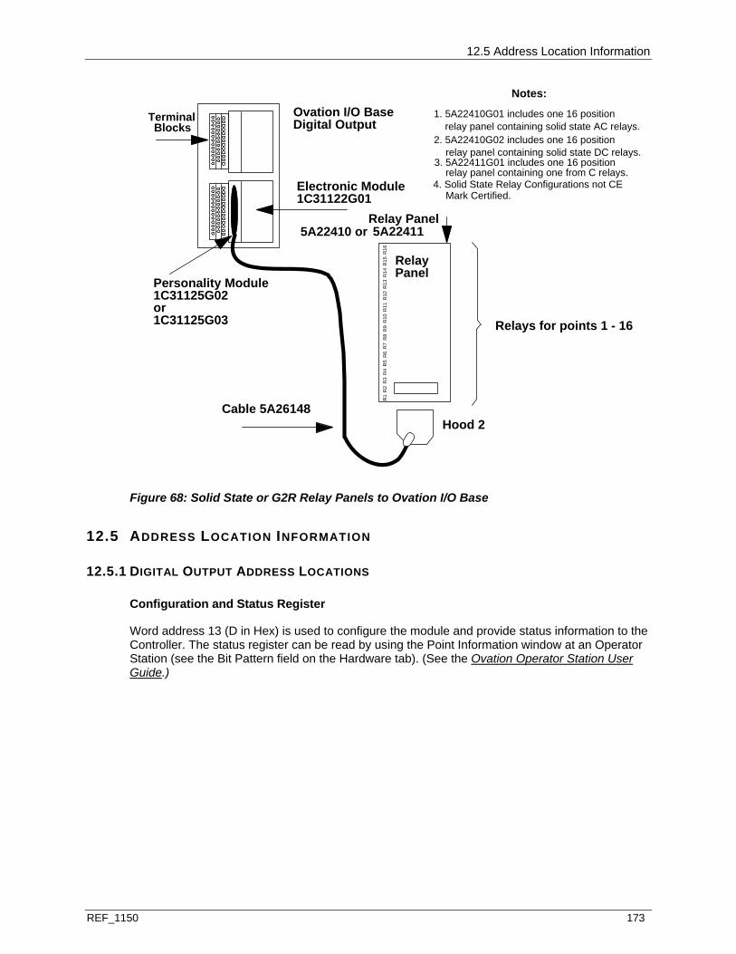
12.5 Address Location Information
REF_1150 173
RelayPanel
Hood 2
Relays for points 1 - 16
Electronic Module1C31122G01
Personality Module1C31125G02or1C31125G03
Ovation I/O BaseDigital Output
Cable 5A26148
TerminalBlocks
Relay Panel 5A22411
R1
R8
R2
R3
R4
R5
R6
R7
R9
R16
R10
R11
R12
R13
R14
R15
4. Solid State Relay Configurations not CE
5A22410 or
1. 5A22410G01 includes one 16 position
Notes:
2. 5A22410G02 includes one 16 positionrelay panel containing solid state AC relays.
relay panel containing solid state DC relays.3. 5A22411G01 includes one 16 position
relay panel containing one from C relays.
Mark Certified.
Figure 68: Solid State or G2R Relay Panels to Ovation I/O Base
12.5 ADDRESS LOCATION INFORMATION
12.5.1 DIGITAL OUTPUT ADDRESS LOCATIONS
Configuration and Status Register
Word address 13 (D in Hex) is used to configure the module and provide status information to the Controller. The status register can be read by using the Point Information window at an Operator Station (see the Bit Pattern field on the Hardware tab). (See the Ovation Operator Station User Guide.)
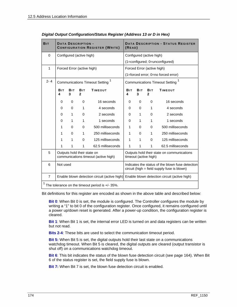
12.5 Address Location Information
174 REF_1150
Digital Output Configuration/Status Register (Address 13 or D in Hex)
BI T DAT A DE S C R I P T I O N - CO N FI G U R AT I O N REGI S TE R (WRI TE)
DAT A DE S C R I P T I O N - ST ATUS REGI S TER (RE AD)
0 Configured (active high) Configured (active high)
(1=configured; 0=unconfigured)
1 Forced Error (active high) Forced Error (active high)
(1=forced error; 0=no forced error)
2- 4 Communications Timeout Setting 1
BI T 4
BI T 3
BI T 2
T I M EO U T
0 0 0 16 seconds
0 0 1 4 seconds
0 1 0 2 seconds
0 1 1 1 seconds
1 0 0 500 milliseconds
1 0 1 250 milliseconds
1 1 0 125 milliseconds
1 1 1 62.5 milliseconds
Communications Timeout Setting 1
BI T 4
BI T 3
BI T 2
T I M EO U T
0 0 0 16 seconds
0 0 1 4 seconds
0 1 0 2 seconds
0 1 1 1 seconds
1 0 0 500 milliseconds
1 0 1 250 milliseconds
1 1 0 125 milliseconds
1 1 1 62.5 milliseconds 5 Outputs hold their state on
communications timeout (active high) Outputs hold their state on communications timeout (active high)
6 Not used Indicates the status of the blown fuse detection circuit (high = field supply fuse is blown)
7 Enable blown detection circuit (active high) Enable blown detection circuit (active high)
1 The tolerance on the timeout period is +/- 35%.
Bit definitions for this register are encoded as shown in the above table and described below:
Bit 0: When Bit 0 is set, the module is configured. The Controller configures the module by writing a “1” to bit 0 of the configuration register. Once configured, it remains configured until a power up/down reset is generated. After a power-up condition, the configuration register is cleared.
Bit 1: When Bit 1 is set, the internal error LED is turned on and data registers can be written but not read.
Bits 2-4: These bits are used to select the communication timeout period.
Bit 5: When Bit 5 is set, the digital outputs hold their last state on a communications watchdog timeout. When Bit 5 is cleared, the digital outputs are cleared (output transistor is shut off) on a communications watchdog timeout.
Bit 6: This bit indicates the status of the blown fuse detection circuit (see page 164). When Bit 6 of the status register is set, the field supply fuse is blown.
Bit 7: When Bit 7 is set, the blown fuse detection circuit is enabled.
12.6 Diagnostic LEDs
REF_1150 175
12.6 DIAGNOSTIC LEDS
The following table lists the module’s LEDs and describes what they mean when lit.
Digital Output Diagnostic LEDs
LED DE S C RI P TI O N
P (Green) Power OK LED. Lit when the +5V power is OK.
C (Green) Communications OK LED. Lit when the Controller is communicating with the module.
E (Red) External Fault LED. Lit when the field supply fuse is blown and the blown fuse detection circuit is enabled. Blown Fuse bit (Bit 7) of the Configuration Register (see page 173) enables or disables the fuse detection circuit (high = enabled).
I (Red) Internal Fault LED. Lit whenever the Force Error bit (Bit 1 of the Configuration Register (see page 173)) is active, or the Controller stops communicating with the module.
CH1 - CH 16 (Green)
If the LED is lit, this indicates that the output is in the ON state.
If the LED is not lit, this indicates that the output is in the OFF state.
12.7 SPECIFICATIONS
Electronics Module (1C31122)
Personality Module (1C31125)
Digital Output Module Specifications
DE S C RI P TI O N VALUE
Number of channels 16
Output voltage
Off voltage (maximum)
On voltage (maximum)
60 VDC
1.0 V @ 500mA
0.2 V @ 100mA
12.7 Specifications
176 REF_1150
DE S C RI P TI O N VALUE
Output current
Off current (maximum)
On current for all 16 outputs combined (max)
Personality module Group 1
Personality module Group 2 1
Personality module Group 3 1
On current for individual output (max)
25μA @ TA = 25°C, VDS = 60 VDC
250μA @ TA = 60°C, VDS = 60 VDC
Limited by fuse rating
890mA maximum for all 16 outputs
2.2A maximum for all 16 outputs
Limited by the fuse located on the relay module
500 mA
Blown fuse detection 2
Operating voltage range
15V ≤ field supply voltage ≤ 60V
Maximum propagation time 2.5 mSec for Rload=500Ω
Dielectric isolation: 3
Channel to logic
1000V AC/DC
Module power Main: 2.2 W typical, 3.3 W maximum
Aux used with no relay panels:
8 outputs on @ 100mA each
19.2 W (24V) typical
38.4 W (48V) typical
Aux used with the following relay panels:
Solid State panel with 16 relays: 5.9 W (24V) typical
G2R panel with 16 relays: 10.87 W (24V) typical
KUEP panel with 8 Form C relays: 15.84 W (24V) typical
2 KUEP panels with 16 Form C relays: 31.68 W (24V)typical
KUEP panel with 8 Form X relays: 11.28 W (24V) typical
2 KUEP panels with 16 Form X relays: 22.56 W (24V)typical
Operating temperature range 0 to 60°C (32°F to 140°F)
Storage temperature range -40°C to 85°C (-40°F to 185°F)
Humidity (non-condensing) 0 to 95%
1 The personality module Groups 2 and 3 are used to interface with the relay modules (see page 153).2 The user can configure the card to disable the blown fuse detection function.
3 All 16 channels have a common return which is isolated from the logic ground.
REF_1150 177
IN THIS SECTION
Description ......................................................................................................................177 Module Group Information ..............................................................................................177 Module Specific Information............................................................................................179 Wiring Information ...........................................................................................................182 Address Location Information .........................................................................................188 Diagnostic LEDs..............................................................................................................191 Specifications ..................................................................................................................192
13.1 DESCRIPTION
HART (Highway Addressable Remote Transducer) is a digital communication protocol designed for industrial process measurement applications. Field measurement devices (transmitters) interface a process control system via an analog 4-to-20 mA current loop. HART uses a low-level frequency shift-keyed sine wave signal that is superimposed on the standard 4-to-20 mA process measurement current loop. Since the HART sine wave signal is small and its average value is zero, the current loop analog 4-to-20 mA signal is not significantly affected by the presence of the HART signal. Using HART allows a field device to provide more than one measurement, which is a feature not available when using only the 4-to-20 A analog current signal.
“Smart” field devices may be described as field devices in which the analog 4-to-20 mA signal, digital communication, and sometimes power, co-exist on the same pair of wires. The Ovation HART Analog Input (HAI) module is a standard form factor Ovation I/O module, which will permit Ovation to communicate with HART devices.
The HART Analog Input Module is applicable for CE Mark configured systems.
Note: I/O Module General Information (see page 15) contains environmental, installation, wiring, and fuse information for I/O modules.
13.2 MODULE GROUP INFORMATION
13.2.1 ELECTRONICS MODULE (EMOD)
There is one Electronics Module group for the HART Analog Input Module:
5X00058G01 interfaces to eight current loop signals with an input range of 4-20 mA.
S E C T I O N 1 3
HART ANALOG INPUT MODULE
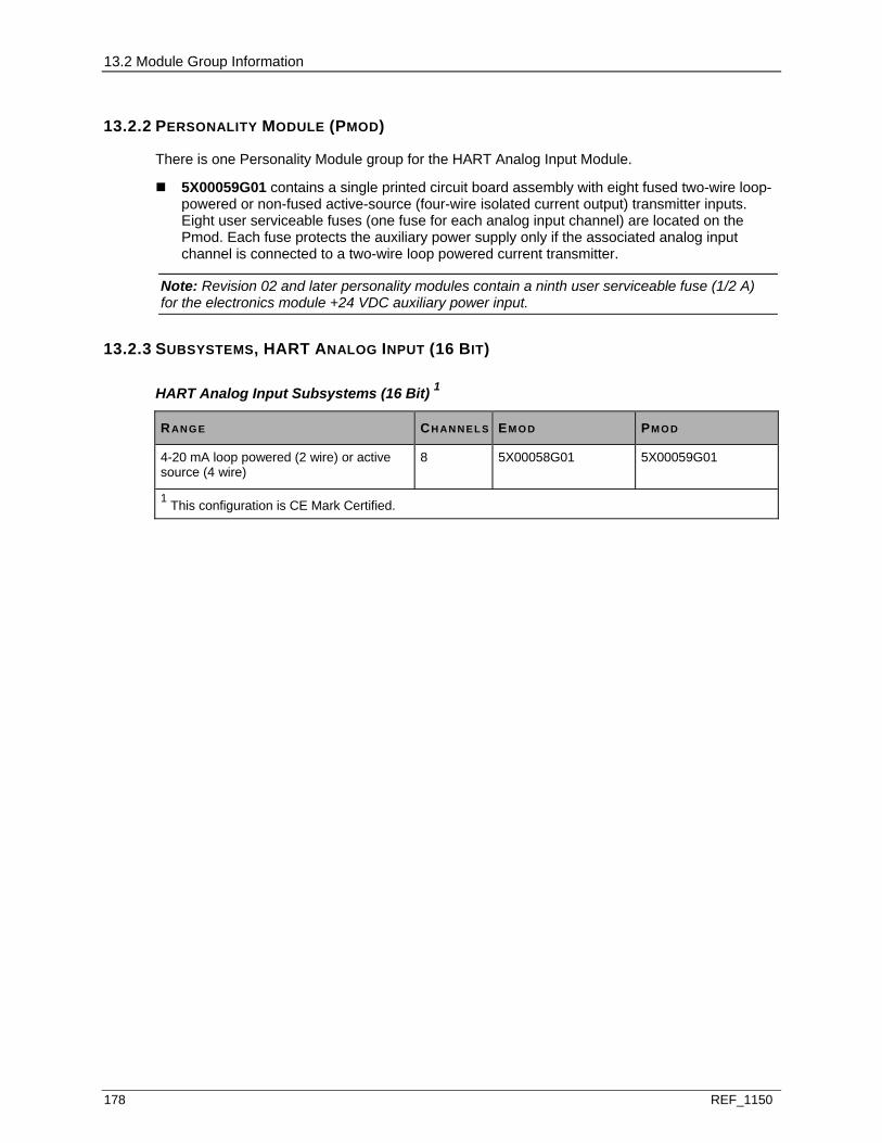
13.2 Module Group Information
178 REF_1150
13.2.2 PERSONALITY MODULE (PMOD)
There is one Personality Module group for the HART Analog Input Module.
5X00059G01 contains a single printed circuit board assembly with eight fused two-wire loop-powered or non-fused active-source (four-wire isolated current output) transmitter inputs. Eight user serviceable fuses (one fuse for each analog input channel) are located on the Pmod. Each fuse protects the auxiliary power supply only if the associated analog input channel is connected to a two-wire loop powered current transmitter.
Note: Revision 02 and later personality modules contain a ninth user serviceable fuse (1/2 A) for the electronics module +24 VDC auxiliary power input.
13.2.3 SUBSYSTEMS, HART ANALOG INPUT (16 BIT)
HART Analog Input Subsystems (16 Bit) 1
RANG E CH AN N E L S EM O D PM O D
4-20 mA loop powered (2 wire) or active source (4 wire)
8 5X00058G01 5X00059G01
1 This configuration is CE Mark Certified.
13.3 Module Specific Information
REF_1150 179
13.3 MODULE SPECIFIC INFORMATION
13.3.1 MODULE BLOCK DIAGRAM
The Ovation HART Analog Input Module assembly consists of two modules: an electronics module containing a logic printed circuit board (LHA) and a field printed circuit board (FHI). The simplified block diagram for the FHI field board is shown below. The electronics module is used in conjunction with a personality module, which contains a single printed circuit board (PHAI).
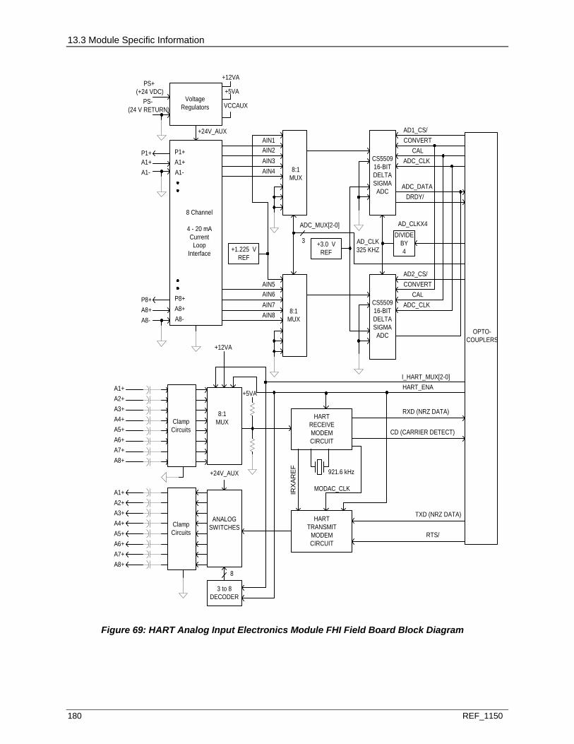
13.3 Module Specific Information
180 REF_1150
P1+A1+A1-
P8+A8+A8-
8 Channel
4 - 20 mACurrent
LoopInterface
AIN1AIN2AIN3AIN4
AIN5AIN6AIN7AIN8
+1.225 VREF
8:1MUX
8:1MUX
+3.0 VREF
CS550916-BITDELTASIGMA
ADC
CS550916-BITDELTASIGMA
ADC
AD1_CS/CONVERT
CALADC_CLK
AD2_CS/CONVERT
CALADC_CLK
ADC_DATADRDY/
ADC_MUX[2-0]
3DIVIDE
BY4
AD_CLKX4
AD_CLK325 KHZ
A1+
A8+
A1+A2+A3+A4+A5+A6+A7+A8+
8:1MUX
HARTRECEIVEMODEMCIRCUIT
RXD (NRZ DATA)
CD (CARRIER DETECT)
HARTTRANSMIT
MODEMCIRCUIT
A1+A2+A3+A4+A5+A6+A7+A8+
P1+
A1-
P8+
A8-
ANALOGSWITCHES
3 to 8DECODER
8
TXD (NRZ DATA)
RTS/
HART_ENAI_HART_MUX[2-0]
OPTO-COUPLERS
VoltageRegulators
PS+ (+24 VDC)
PS- (24 V RETURN)
+12VA
+5VA
VCCAUX
+5VA
+24V_AUX
+12VA
ClampCircuits
ClampCircuits
+24V_AUX
MODAC_CLK
921.6 kHz
IRXA
REF
Figure 69: HART Analog Input Electronics Module FHI Field Board Block Diagram

13.3 Module Specific Information
REF_1150 181
13.3.2 EXTERNAL POWER SUPPLIES
Note: Module power specifications (main and auxiliary) refer to the actual power drawn by the module from the 24 VDC main power supply and from the +24 VDC auxiliary power supply and NOT from the AC or DC mains.
The HART Analog Input Module utilizes the standard +24V Ovation main power supply to provide the power required for the logic circuitry.
The HART Analog Input Module utilizes a +24 auxiliary power supply to provide the power required for the field circuitry. This includes all 4-20 mA loop power, A/D conversion, and the remaining output channel components.
It is recommended that the HART Analog Input module utilize the Ovation cabinet’s Auxiliary +24V DC power that is obtained from the standard Ovation DIN Rail power supply auxiliary output.
However, if an external auxiliary power supply is utilized by the HART Analog Input module, the power supply output noise cannot exceed 2.2 mVRMS Maximum for all rated loads across the frequency range of 500 HZ to 10 kHZ, see the following figure.
mV RMS
138OutputNoise and Ripple 2.2
47 Hz 63 Hz 500 Hz 10 kHz 3.2 MHz Frequency (in Hz)
707
+20 dB/dec-40 dB/dec
Figure 70: Power Supply Output Noise Requirements
If an external power supply is used, Using an External Power Supply (see page 539) contains steps to be undertaken before connecting the external power supply to the Ovation I/O base unit terminal block.
In addition, all modules utilizing the auxiliary power supplies, including the HART modules, MUST utilize shielded I/O cables in order to suppress coupled noise and transients into the HART modules. This includes modules on the same branch utilizing the auxiliary power, or modules on other branches utilizing the same auxiliary power. This recommendation applies regardless of the type of power supply chosen by the user.
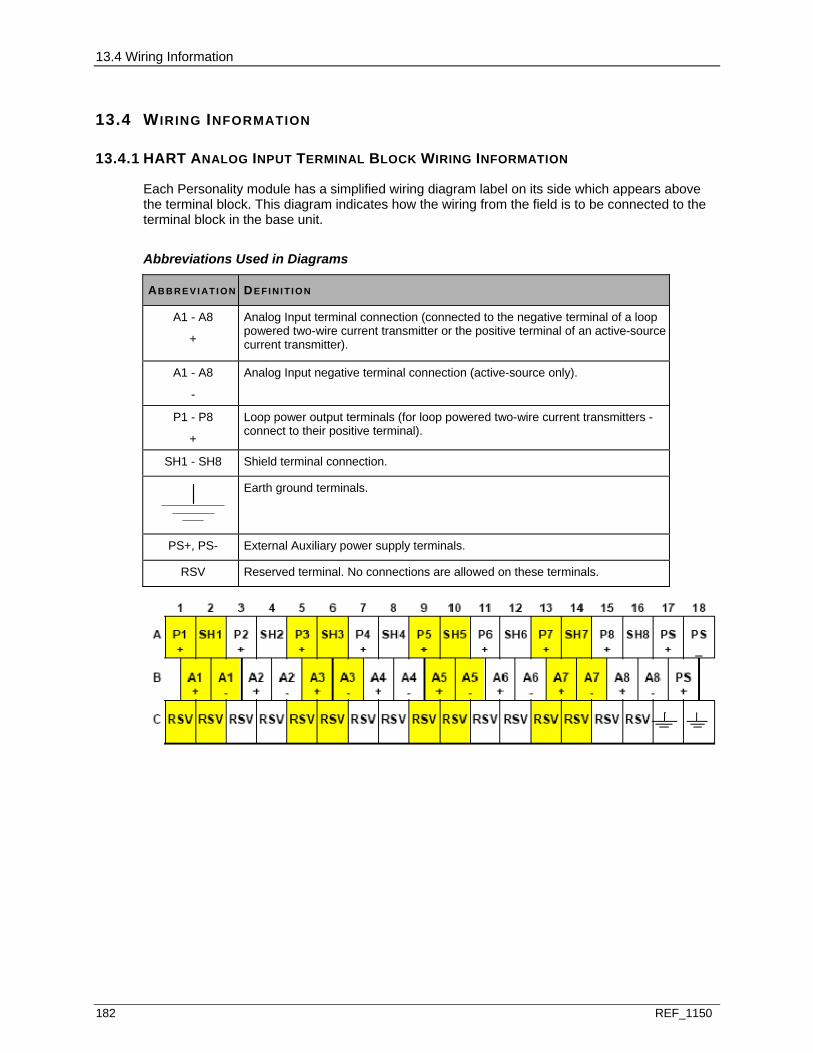
13.4 Wiring Information
182 REF_1150
13.4 WIRING INFORMATION
13.4.1 HART ANALOG INPUT TERMINAL BLOCK WIRING INFORMATION
Each Personality module has a simplified wiring diagram label on its side which appears above the terminal block. This diagram indicates how the wiring from the field is to be connected to the terminal block in the base unit.
Abbreviations Used in Diagrams
AB B R E V I AT I ON DE FI NI T I O N
A1 - A8
+
Analog Input terminal connection (connected to the negative terminal of a loop powered two-wire current transmitter or the positive terminal of an active-source current transmitter).
A1 - A8
-
Analog Input negative terminal connection (active-source only).
P1 - P8
+
Loop power output terminals (for loop powered two-wire current transmitters - connect to their positive terminal).
SH1 - SH8 Shield terminal connection.
Earth ground terminals.
PS+, PS- External Auxiliary power supply terminals.
RSV Reserved terminal. No connections are allowed on these terminals.

13.4 Wiring Information
REF_1150 183
13.4.2 HART ANALOG INPUT FIELD CONNECTION WIRING DIAGRAMS (NON-CE MARK CERTIFIED SYSTEMS)
Figure 71: HART Analog Input Connections (Non CE Mark)
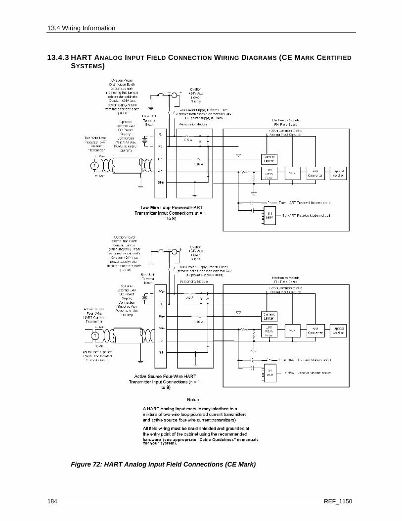
13.4 Wiring Information
184 REF_1150
13.4.3 HART ANALOG INPUT FIELD CONNECTION WIRING DIAGRAMS (CE MARK CERTIFIED SYSTEMS)
Figure 72: HART Analog Input Field Connections (CE Mark)
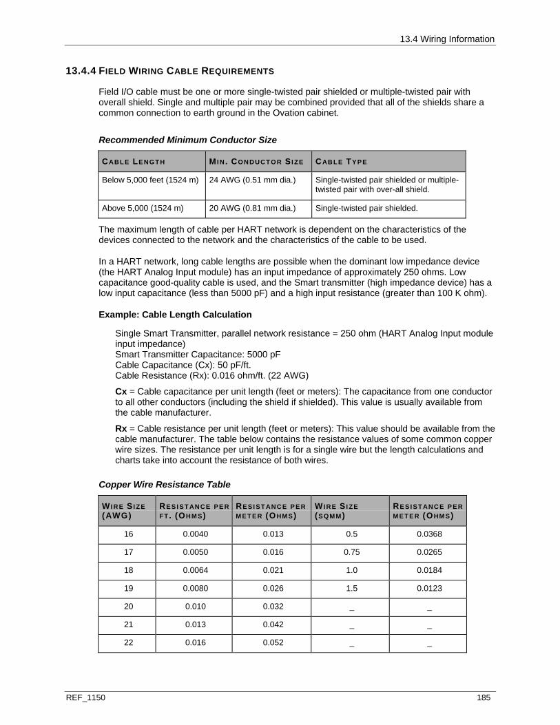
13.4 Wiring Information
REF_1150 185
13.4.4 FIELD WIRING CABLE REQUIREMENTS
Field I/O cable must be one or more single-twisted pair shielded or multiple-twisted pair with overall shield. Single and multiple pair may be combined provided that all of the shields share a common connection to earth ground in the Ovation cabinet.
Recommended Minimum Conductor Size
CABL E LE NGTH MI N. CO N D UC T O R SI ZE CABLE TY PE
Below 5,000 feet (1524 m) 24 AWG (0.51 mm dia.) Single-twisted pair shielded or multiple-twisted pair with over-all shield.
Above 5,000 (1524 m) 20 AWG (0.81 mm dia.) Single-twisted pair shielded.
The maximum length of cable per HART network is dependent on the characteristics of the devices connected to the network and the characteristics of the cable to be used.
In a HART network, long cable lengths are possible when the dominant low impedance device (the HART Analog Input module) has an input impedance of approximately 250 ohms. Low capacitance good-quality cable is used, and the Smart transmitter (high impedance device) has a low input capacitance (less than 5000 pF) and a high input resistance (greater than 100 K ohm).
Example: Cable Length Calculation
Single Smart Transmitter, parallel network resistance = 250 ohm (HART Analog Input module input impedance) Smart Transmitter Capacitance: 5000 pF Cable Capacitance (Cx): 50 pF/ft. Cable Resistance (Rx): 0.016 ohm/ft. (22 AWG)
Cx = Cable capacitance per unit length (feet or meters): The capacitance from one conductor to all other conductors (including the shield if shielded). This value is usually available from the cable manufacturer.
Rx = Cable resistance per unit length (feet or meters): This value should be available from the cable manufacturer. The table below contains the resistance values of some common copper wire sizes. The resistance per unit length is for a single wire but the length calculations and charts take into account the resistance of both wires.
Copper Wire Resistance Table
WI RE SI ZE (AWG)
RE SI ST AN C E P E R F T. (OHM S)
RE SI ST AN C E P E R M ET E R (OHMS)
WI RE S I ZE (S QM M)
RE SI ST AN C E P E R M ET E R (OHMS)
16 0.0040 0.013 0.5 0.0368
17 0.0050 0.016 0.75 0.0265
18 0.0064 0.021 1.0 0.0184
19 0.0080 0.026 1.5 0.0123
20 0.010 0.032 _ _
21 0.013 0.042 _ _
22 0.016 0.052 _ _
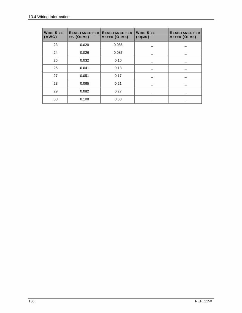
13.4 Wiring Information
186 REF_1150
WI RE SI ZE (AWG)
RE SI ST AN C E P E R F T. (OHM S)
RE SI ST AN C E P E R M ET E R (OHMS)
WI RE S I ZE (S QM M)
RE SI ST AN C E P E R M ET E R (OHMS)
23 0.020 0.066 _ _
24 0.026 0.085 _ _
25 0.032 0.10 _ _
26 0.041 0.13 _ _
27 0.051 0.17 _ _
28 0.065 0.21 _ _
29 0.082 0.27 _ _
30 0.100 0.33 _ _

13.4 Wiring Information
REF_1150 187
From the following figure, using cable capacitance (Cx) of 50 pF/unit length and resistance (Rx) of 0.016 ohm/unit length, a direct reading of the corresponding length on the y-axis is approximately 3600 feet (unit length of feet from above parameters).
Figure 73: Length Graph - Single Device Network

13.5 Address Location Information
188 REF_1150
13.5 ADDRESS LOCATION INFORMATION
13.5.1 CONFIGURATION AND STATUS REGISTER
Each of the 16 direct registers on the HART Analog Input module is summarized here and shown in more detail in the following tables. The status register can be read by using the Point Information window at an Operator’s Station.
HART Analog Input Register Map
RE G DAT A DE S C R I P T I O N - CO N FI G U R AT I O N REGI S TE R (WRI TE)
DAT A DE S C R I P T I O N - ST ATUS REGI S TER (RE AD)
0 Indirect Memory Index NA
1 Indirect Memory Data Indirect Memory Data
2 NA Analog Input - Channel 1
3 NA Analog Input - Channel 2
4 NA Analog Input - Channel 3
5 NA Analog Input - Channel 4
6 NA Analog Input - Channel 5
7 NA Analog Input - Channel 6
8 NA Analog Input - Channel 7
9 NA Analog Input - Channel 8
10 NA Firmware Status Flags
11 NA HAI Firmware Revision
12 NA Channel Error Bits
13 Module Configuration Register Module Status Register (See table below)
14 HART Enable NA
15 NA Module Electronic ID Data
HART AI Configuration/Status Register (Address 13 or D in Hex)
BI T DAT A DE S C R I P T I O N (WRI TE) DAT A DE S C R I P T I O N (RE AD)
0 Configure Module Module Configured (1 = configured; 0 = unconfigured)
1 Force Error Internal or forced error (1 = forced error; 0 = no forced error)
2 Reserved NA

13.5 Address Location Information
REF_1150 189
BI T DAT A DE S C R I P T I O N (WRI TE) DAT A DE S C R I P T I O N (RE AD)
3 Reserved NA
4 Reserved NA
5 Reserved NA
6 Reserved for Factory Test (must always be set to 0)
NA
7 Reserved for Factory Test (must always be set to 0)
NA
8 NA Hardware Error
9 NA Bank 1 reference error
10 NA Bank 2 reference error
11 Not Used Not Used
12 Not Used Not Used
13 Not Used Not Used
14 NA Field power failed
15 Reserved Reserved
Bit definitions for this register are encoded as shown in the above table are described below:
Bit 0: This bit configures the module (write) or indicates the configuration state of module (read). A “1” indicates that the module is configured.
Bit 1: Forces the module into error state, illuminating the module’s Error LED.
Bits 2 - 5, 11 - 13: Not used by the module.
Bits 6 - 7: Reserved for factory test, must always be set to 0.
Bit 8: Hardware error. Indicates one or more of the following is true:
- The FPGA did not program correctly on startup. - The EE memory checksum is incorrect. - The PROM checksum test has failed. - Internal memory diagnostic has failed.
Bit 9: Reference error on first mux/AD combination.
Bit 10: Reference error on second mux/AD combination.
Bit 14: Field power failed.
Bit 15: Reserved.

13.5 Address Location Information
190 REF_1150
13.5.2 HART ANALOG INPUT ENABLE REGISTER (ADDRESS 14 OR E IN HEX)
HART Analog Input Enable Register (Address 14 or E in Hex)
BI T DAT A DE S C R I P T I O N - CO N FI G U R AT I O N REGI S TE R (WRI TE)
DAT A DE S C R I P T I O N - ST ATUS REGI S TER (RE AD)
0 Multivariable Channel 1 Not Used
1 Multivariable Channel 2 Not Used
2 Multivariable Channel 3 Not Used
3 Multivariable Channel 4 Not Used
4 Multivariable Channel 5 Not Used
5 Multivariable Channel 6 Not Used
6 Multivariable Channel 7 Not Used
7 Multivariable Channel 8 Not Used
8 HART Enabled - Channel 1 Not Used
9 HART Enabled - Channel 2 Not Used
10 HART Enabled - Channel 3 Not Used
11 HART Enabled - Channel 4 Not Used
12 HART Enabled - Channel 5 Not Used
13 HART Enabled - Channel 6 Not Used
14 HART Enabled - Channel 7 Not Used
15 HART Enabled - Channel 8 Not Used

13.6 Diagnostic LEDs
REF_1150 191
Bit definitions for this register are encoded as shown in the above table and described below:
Bits 0-7: These bits are set to enable multivariable messaging. Refer to the IO configuration guide for additional information.
The HAI, HAO, and IAH modules have the ability to retrieve additional variables from a field device. These variables are referred to as ‘multivariables’ and are named PV (primary variable), SV (secondary variable), TV (tertiary variable), and QV (quarterly variable).
If the bit is set, the module will periodically retrieve whatever variables exist for the device.
The definitions of PV, SV, TV, and QV are found in the user’s manual for the field device supplied by the device manufacturer. The standard format of these four variables is IEEE 794, a floating-point format.
You must configure IO point records to cause the Controller to scan the module and retrieve the variables. (See the Point Builder User Guide or Developer Studio User Guide.)
Bits 8-15: In the IO configuration tool, you can set these flags on a per-channel basis to allow HART messaging, including multivariable messaging, to flow on that channel.
You should ensure that these bits are cleared for non-HART field devices. To avoid a HART communication error message, set each bit at “0” when connecting a non-HART output device.
13.6 DIAGNOSTIC LEDS
The following table lists the module’s LEDs and describes what they mean when lit.
HART Analog Input Diagnostic LEDs
LED DE S C RI P TI O N
P (Green) Power OK LED. Illuminated when the +5V power is OK.
C (Green) Communications OK LED. Illuminated when the Controller is communicating with the module.
E (Red) External Error LED. Illuminated upon loss of external auxiliary (field) power, as indicated by the loss of normal transitions of the EOC (end-of-convert) signal.
I (Red) Internal Error LED. Illuminated whenever there is any type of error within the module except for a loss of external auxiliary power. Possible causes are: The Controller sets the module’s Force Error bit. Communications with the Controller is lost. The ground or reference reading is out of range. Flash memory, EE memory or RAM diagnostic failure.
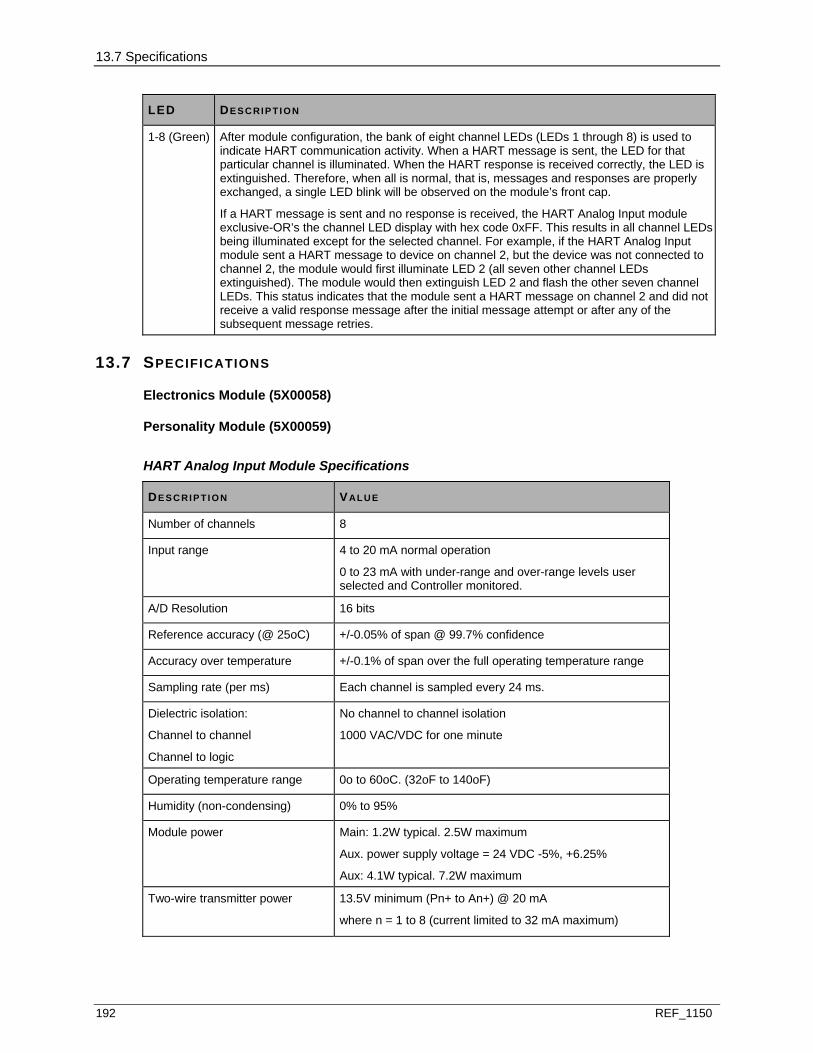
13.7 Specifications
192 REF_1150
LED DE S C RI P TI O N
1-8 (Green) After module configuration, the bank of eight channel LEDs (LEDs 1 through 8) is used to indicate HART communication activity. When a HART message is sent, the LED for that particular channel is illuminated. When the HART response is received correctly, the LED is extinguished. Therefore, when all is normal, that is, messages and responses are properly exchanged, a single LED blink will be observed on the module’s front cap.
If a HART message is sent and no response is received, the HART Analog Input module exclusive-OR’s the channel LED display with hex code 0xFF. This results in all channel LEDs being illuminated except for the selected channel. For example, if the HART Analog Input module sent a HART message to device on channel 2, but the device was not connected to channel 2, the module would first illuminate LED 2 (all seven other channel LEDs extinguished). The module would then extinguish LED 2 and flash the other seven channel LEDs. This status indicates that the module sent a HART message on channel 2 and did not receive a valid response message after the initial message attempt or after any of the subsequent message retries.
13.7 SPECIFICATIONS
Electronics Module (5X00058)
Personality Module (5X00059)
HART Analog Input Module Specifications
DE S C RI P TI O N VALUE
Number of channels 8
Input range 4 to 20 mA normal operation
0 to 23 mA with under-range and over-range levels user selected and Controller monitored.
A/D Resolution 16 bits
Reference accuracy (@ 25oC) +/-0.05% of span @ 99.7% confidence
Accuracy over temperature +/-0.1% of span over the full operating temperature range
Sampling rate (per ms) Each channel is sampled every 24 ms.
Dielectric isolation:
Channel to channel
Channel to logic
No channel to channel isolation
1000 VAC/VDC for one minute
Operating temperature range 0o to 60oC. (32oF to 140oF)
Humidity (non-condensing) 0% to 95%
Module power Main: 1.2W typical. 2.5W maximum
Aux. power supply voltage = 24 VDC -5%, +6.25%
Aux: 4.1W typical. 7.2W maximum
Two-wire transmitter power 13.5V minimum (Pn+ to An+) @ 20 mA
where n = 1 to 8 (current limited to 32 mA maximum)
REF_1150 193
IN THIS SECTION
Description ......................................................................................................................193 Module Group Information ..............................................................................................194 Module Specific Information............................................................................................195 Wiring Information ...........................................................................................................198 Address Location Information .........................................................................................200 Diagnostic LEDs..............................................................................................................204 Specifications ..................................................................................................................204
14.1 DESCRIPTION
The HART (Highway Addressable Remote Transducer) High Performance (HP) Analog Input module is a standard Ovation I/O Module that provides eight galvanically isolated 4-20 mA analog inputs with HART transceivers. Each transceivers provides optically isolated communication to a dedicated UART (Universal Addressable Remote Transducer), thereby maximizing HART communication throughout. Each channel may be individually configured for field powered or local powered transmitters via user accessible jumpers on the Personality Module.
HART is a digital communication protocol designed for industrial process measurement applications. Field measurement devices (transmitters) interface for a process control system via an analog 4-to-20 mA current loop. HART uses a low-level frequency-shift-keyed sine wave signal that is superimposed on the standard 4-to-20 mA process measurement current loop. Since the HART sine wave signal is small and its average value is zero, the current loop analog 4-to-20 mA signal is not significantly affected by the presence of the HART signal. Using HART allows a field device to provide more than one measurement, which is a feature not available when using only the 4-to-20mA analog current signal.
“Smart” field devices may be described as field devices in which the analog 4-to-20 mA signal, digital communication, and sometimes power, co-exist on the same pair of wires. The Ovation HART High Performance Analog Input (IAH) module is a standard form factor Ovation I/O module, which will permit Ovation to communicate with HART devices.
Note: I/O Module General Information (see page 15) contains environmental, installation, wiring, and fuse information for I/O modules.
S E C T I O N 1 4
HART HIGH PERFORMANCE ANALOG INPUT MODULE
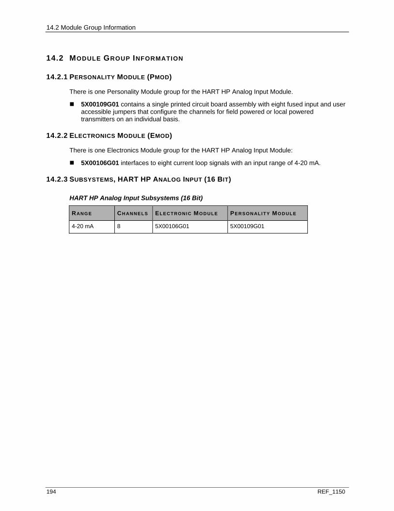
14.2 Module Group Information
194 REF_1150
14.2 MODULE GROUP INFORMATION
14.2.1 PERSONALITY MODULE (PMOD)
There is one Personality Module group for the HART HP Analog Input Module.
5X00109G01 contains a single printed circuit board assembly with eight fused input and user accessible jumpers that configure the channels for field powered or local powered transmitters on an individual basis.
14.2.2 ELECTRONICS MODULE (EMOD)
There is one Electronics Module group for the HART HP Analog Input Module:
5X00106G01 interfaces to eight current loop signals with an input range of 4-20 mA.
14.2.3 SUBSYSTEMS, HART HP ANALOG INPUT (16 BIT)
HART HP Analog Input Subsystems (16 Bit)
RANG E CH AN N E L S EL E CT RO NI C MO D U LE PE R S O N AL I T Y MODULE
4-20 mA 8 5X00106G01 5X00109G01
14.3 Module Specific Information
REF_1150 195
14.3 MODULE SPECIFIC INFORMATION
14.3.1 MODULE BLOCK DIAGRAM AND FIELD CONNECTION WIRING DIAGRAM
The Ovation HART HP Analog Input Module subsystem consists of two modules, an electronics module containing a logic printed circuit board (LIH) and a field printed circuit board (FIH). The electronics module is used in conjunction with a personality module, which contains a single printed circuit board (PIHA).

14.3 Module Specific Information
196 REF_1150
Figure 74: HART HP Analog Input Subsystem Block Diagram
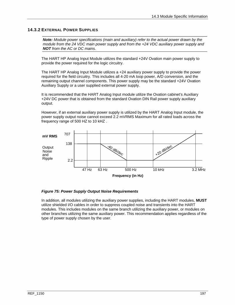
14.3 Module Specific Information
REF_1150 197
14.3.2 EXTERNAL POWER SUPPLIES
Note: Module power specifications (main and auxiliary) refer to the actual power drawn by the module from the 24 VDC main power supply and from the +24 VDC auxiliary power supply and NOT from the AC or DC mains.
The HART HP Analog Input Module utilizes the standard +24V Ovation main power supply to provide the power required for the logic circuitry.
The HART HP Analog Input Module utilizes a +24 auxiliary power supply to provide the power required for the field circuitry. This includes all 4-20 mA loop power, A/D conversion, and the remaining output channel components. This power supply may be the standard +24V Ovation Auxiliary Supply or a user supplied external power supply.
It is recommended that the HART Analog Input module utilize the Ovation cabinet’s Auxiliary +24V DC power that is obtained from the standard Ovation DIN Rail power supply auxiliary output.
However, if an external auxiliary power supply is utilized by the HART Analog Input module, the power supply output noise cannot exceed 2.2 mVRMS Maximum for all rated loads across the frequency range of 500 HZ to 10 kHZ .
mV RMS
138OutputNoise and Ripple 2.2
47 Hz 63 Hz 500 Hz 10 kHz 3.2 MHz Frequency (in Hz)
707
+20 dB/dec-40 dB/dec
Figure 75: Power Supply Output Noise Requirements
In addition, all modules utilizing the auxiliary power supplies, including the HART modules, MUST utilize shielded I/O cables in order to suppress coupled noise and transients into the HART modules. This includes modules on the same branch utilizing the auxiliary power, or modules on other branches utilizing the same auxiliary power. This recommendation applies regardless of the type of power supply chosen by the user.

14.4 Wiring Information
198 REF_1150
14.4 WIRING INFORMATION
14.4.1 HART HP ANALOG INPUT PERSONALITY MODULE INFORMATION
Each Personality module provides a 1/20 A fuse on each channel for loop protection. Additionally, each channel provides a pair of user accessible jumpers for configuring each channel for local powered transmitters or field powered transmitters. This configuration is on a per channel basis. The fuses and jumpers are accessible through the top of the module. The label, shown in the following figure, on the top of the module indicates how to position the jumpers. Note that there are two jumpers per channel and they must be positioned together.
Figure 76: HART HP Analog Input Personality Module
Note: Jumpers are shown in the local powered configuration for all channels.
14.4.2 HART HP ANALOG INPUT TERMINAL BLOCK WIRING INFORMATION
Each Personality module has a simplified wiring diagram label on its side which appears above the terminal block. This diagram indicates how the wiring from the field is to be connected to the terminal block in the base unit. Note that there are two wiring configurations for each channel dependant upon whether the channel is configured for Local or Field powered transmitters.
Figure 77: Wiring Diagram Label
The diagrams for the HART HP Analog Input Personality modules are illustrated in the figure above. The following table lists and defines the abbreviations used in those diagrams.
Wiring Diagram Label Definitions
AB B R E V I AT I ON AB B R E V I AT I ON
A1 - A8
+
Analog Input terminal connection (connected to the negative terminal of a local powered transmitter or the positive terminal of field powered transmitter).

14.4 Wiring Information
REF_1150 199
AB B R E V I AT I ON AB B R E V I AT I ON
A1 - A8
-
Analog Input negative terminal connection (field powered configuration only).
P1 - P8
+
Loop power output terminals (for local powered configuration only. Connected to the positive).
SH1 - SH8 Shield terminal connection. (For landing shields where the shield is to be grounded at the transmitter).
Earth ground terminals. (For landing shields where the shield is to be grounded at the module).
PS+, PS- External Auxiliary power supply terminals.
RSV Reserved terminal. No connections are allowed on these terminals.
14.4.3 FIELD WIRING CABLE REQUIREMENTS
Recommended Minimum Conductor Size
CABL E LE NGTH MI N. CO N D UC T O R SI ZE CABLE TY PE
Less than 5,000 feet (1524 m) 24 AWG (0.51 mm dia.) Single-twisted pair with over-all shield.
Greater than 5,000 feet, but less than 10,000 feet (3048 meters)
20 AWG (0.81 mm dia.) Single-twisted pair with over-all shield.
Refer to the HART FSK Physical Layer Specification (HFC_SPEC-54) for additional cabling information.
The point data registers occupy locations 2-9 for analog input points 1-8 respectively. The data format is as follows:
Bit 15 Bit 14 Bit 13 - 0
14 bit value
Over-range Bit
Point quality: (for good point quality (and proper card operation))
Example Values
Output Data in Hex Data Description
8000 Zero Input
8001 + 1
C000 + Full Scale
CZZZ + Over Range
*0000-7FFF *Card Trouble/Not Warmed Up/Bad Quality
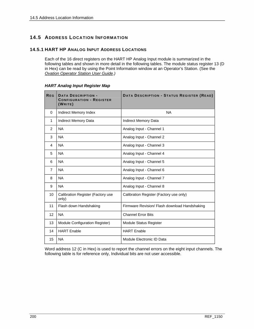
14.5 Address Location Information
200 REF_1150
14.5 ADDRESS LOCATION INFORMATION
14.5.1 HART HP ANALOG INPUT ADDRESS LOCATIONS
Each of the 16 direct registers on the HART HP Analog Input module is summarized in the following tables and shown in more detail in the following tables. The module status register 13 (D in Hex) can be read by using the Point Information window at an Operator’s Station. (See the Ovation Operator Station User Guide.)
HART Analog Input Register Map
RE G DAT A DE S C R I P T I O N - CO N FI G U R AT I O N - REGI STE R (WRI TE)
DAT A DE S C R I P T I O N - ST ATUS REGI S TER (RE AD)
0 Indirect Memory Index NA
1 Indirect Memory Data Indirect Memory Data
2 NA Analog Input - Channel 1
3 NA Analog Input - Channel 2
4 NA Analog Input - Channel 3
5 NA Analog Input - Channel 4
6 NA Analog Input - Channel 5
7 NA Analog Input - Channel 6
8 NA Analog Input - Channel 7
9 NA Analog Input - Channel 8
10 Calibration Register (Factory use only)
Calibration Register (Factory use only)
11 Flash down Handshaking Firmware Revision/ Flash download Handshaking
12 NA Channel Error Bits
13 Module Configuration Register) Module Status Register
14 HART Enable HART Enable
15 NA Module Electronic ID Data
Word address 12 (C in Hex) is used to report the channel errors on the eight input channels. The following table is for reference only, Individual bits are not user accessible.
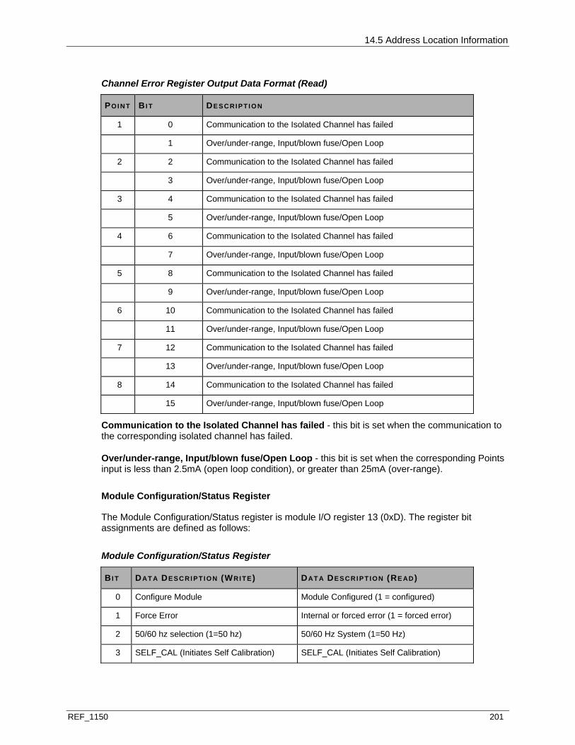
14.5 Address Location Information
REF_1150 201
Channel Error Register Output Data Format (Read)
POI NT BI T DE S C RI P TI O N
1 0 Communication to the Isolated Channel has failed
1 Over/under-range, Input/blown fuse/Open Loop
2 2 Communication to the Isolated Channel has failed
3 Over/under-range, Input/blown fuse/Open Loop
3 4 Communication to the Isolated Channel has failed
5 Over/under-range, Input/blown fuse/Open Loop
4 6 Communication to the Isolated Channel has failed
7 Over/under-range, Input/blown fuse/Open Loop
5 8 Communication to the Isolated Channel has failed
9 Over/under-range, Input/blown fuse/Open Loop
6 10 Communication to the Isolated Channel has failed
11 Over/under-range, Input/blown fuse/Open Loop
7 12 Communication to the Isolated Channel has failed
13 Over/under-range, Input/blown fuse/Open Loop
8 14 Communication to the Isolated Channel has failed
15 Over/under-range, Input/blown fuse/Open Loop
Communication to the Isolated Channel has failed - this bit is set when the communication to the corresponding isolated channel has failed.
Over/under-range, Input/blown fuse/Open Loop - this bit is set when the corresponding Points input is less than 2.5mA (open loop condition), or greater than 25mA (over-range).
Module Configuration/Status Register
The Module Configuration/Status register is module I/O register 13 (0xD). The register bit assignments are defined as follows:
Module Configuration/Status Register
BI T DAT A DE S C R I P T I O N (WRI TE) DAT A DE S C R I P T I O N (RE AD)
0 Configure Module Module Configured (1 = configured)
1 Force Error Internal or forced error (1 = forced error)
2 50/60 hz selection (1=50 hz) 50/60 Hz System (1=50 Hz)
3 SELF_CAL (Initiates Self Calibration) SELF_CAL (Initiates Self Calibration)
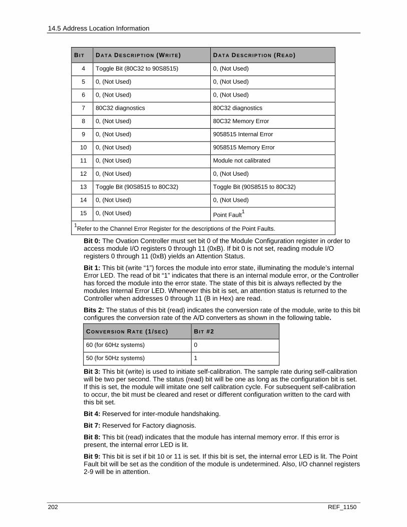
14.5 Address Location Information
202 REF_1150
BI T DAT A DE S C R I P T I O N (WRI TE) DAT A DE S C R I P T I O N (RE AD)
4 Toggle Bit (80C32 to 90S8515) 0, (Not Used)
5 0, (Not Used) 0, (Not Used)
6 0, (Not Used) 0, (Not Used)
7 80C32 diagnostics 80C32 diagnostics
8 0, (Not Used) 80C32 Memory Error
9 0, (Not Used) 9058515 Internal Error
10 0, (Not Used) 9058515 Memory Error
11 0, (Not Used) Module not calibrated
12 0, (Not Used) 0, (Not Used)
13 Toggle Bit (90S8515 to 80C32) Toggle Bit (90S8515 to 80C32)
14 0, (Not Used) 0, (Not Used)
15 0, (Not Used) Point Fault1
1Refer to the Channel Error Register for the descriptions of the Point Faults.
Bit 0: The Ovation Controller must set bit 0 of the Module Configuration register in order to access module I/O registers 0 through 11 (0xB). If bit 0 is not set, reading module I/O registers 0 through 11 (0xB) yields an Attention Status.
Bit 1: This bit (write “1”) forces the module into error state, illuminating the module’s internal Error LED. The read of bit “1” indicates that there is an internal module error, or the Controller has forced the module into the error state. The state of this bit is always reflected by the modules Internal Error LED. Whenever this bit is set, an attention status is returned to the Controller when addresses 0 through 11 (B in Hex) are read.
Bits 2: The status of this bit (read) indicates the conversion rate of the module, write to this bit configures the conversion rate of the A/D converters as shown in the following table.
CO N VE R SI O N RAT E (1 /SE C) BI T #2
60 (for 60Hz systems) 0
50 (for 50Hz systems) 1
Bit 3: This bit (write) is used to initiate self-calibration. The sample rate during self-calibration will be two per second. The status (read) bit will be one as long as the configuration bit is set. If this is set, the module will imitate one self calibration cycle. For subsequent self-calibration to occur, the bit must be cleared and reset or different configuration written to the card with this bit set.
Bit 4: Reserved for inter-module handshaking.
Bit 7: Reserved for Factory diagnosis.
Bit 8: This bit (read) indicates that the module has internal memory error. If this error is present, the internal error LED is lit.
Bit 9: This bit is set if bit 10 or 11 is set. If this bit is set, the internal error LED is lit. The Point Fault bit will be set as the condition of the module is undetermined. Also, I/O channel registers 2-9 will be in attention.

14.5 Address Location Information
REF_1150 203
Bit 10: This bit (read) indicates that the module has internal memory error (FLASH checksum, Register or Static RAM error). Bit 9 will be set as well.
Bit 11: This bit indicates that the module is not calibrated. Bit 9 will be set as well.
Bit 13: Reserved for inter-module handshaking.
Bit 15: Bit indicates point fault status of the module. It is the logical “OR” of any individual channel error status bits in register C, plus bit 9 of this register. A “0” indicates that all eight points have good quality and no module error exists. When bit 9 of the Status Register is not set, this bit (when set to “1”) indicates that at least one of the points has bad quality. A subsequent read of the Channel Error Register (address C) will reveal the point(s) that have bad quality. The Channel Error Register contains data only when the module fault is due to a bad point quality.
HART HP Analog Input Enable Register (Address 14 or E in Hex)
BI T DAT A DE S C R I P T I O N - CO N FI G U R AT I O N REGI S TE R (WRI TE)
DAT A DE S C R I P T I O N - ST AT US RE GI S T E R (RE AD)
0 Multivariable Channel 1 Not Used
1 Multivariable Channel 2 Not Used
2 Multivariable Channel 3 Not Used
3 Multivariable Channel 4 Not Used
4 Multivariable Channel 5 Not Used
5 Multivariable Channel 6 Not Used
6 Multivariable Channel 7 Not Used
7 Multivariable Channel 8 Not Used
8 HART Enabled - Channel 1 Not Used
9 HART Enabled - Channel 2 Not Used
10 HART Enabled - Channel 3 Not Used
11 HART Enabled - Channel 4 Not Used
12 HART Enabled - Channel 5 Not Used
13 HART Enabled - Channel 6 Not Used
14 HART Enabled - Channel 7 Not Used
15 HART Enabled - Channel 8 Not Used
Bit 0-7: A “1” in any of these bits will cause Multivariable messaging on the corresponding channel.
Bit 8-15 A “1” in any of these bits indicate that a HART compliant device exists on the corresponding channel.
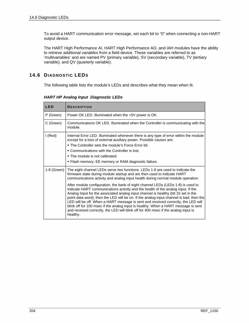
14.6 Diagnostic LEDs
204 REF_1150
To avoid a HART communication error message, set each bit to “0” when connecting a non-HART output device.
The HART High Performance AI, HART High Performance AO, and IAH modules have the ability to retrieve additional variables from a field device. These variables are referred to as ‘multivariables’ and are named PV (primary variable), SV (secondary variable), TV (tertiary variable), and QV (quarterly variable).
14.6 DIAGNOSTIC LEDS
The following table lists the module’s LEDs and describes what they mean when lit.
HART HP Analog Input Diagnostic LEDs
LED DE S C RI P TI O N
P (Green) Power OK LED. Illuminated when the +5V power is OK.
C (Green) Communications OK LED. Illuminated when the Controller is communicating with the module.
I (Red) Internal Error LED. Illuminated whenever there is any type of error within the module except for a loss of external auxiliary power. Possible causes are: The Controller sets the module’s Force Error bit. Communications with the Controller is lost. The module is not calibrated. Flash memory, EE memory or RAM diagnostic failure.
1-8 (Green) The eight channel LEDs serve two functions. LEDs 1-8 are used to indicate the firmware state during module startup and are then used to indicate HART communications activity and analog input health during normal module operation.
After module configuration, the bank of eight channel LEDs (LEDs 1-8) is used to indicate HART communications activity and the health of the analog input. If the Analog Input for the associated analog input channel is healthy (bit 15 set in the point data word), then the LED will be on. If the analog input channel is bad, then the LED will be off. When a HART message is sent and received correctly, the LED will blink off for 100 msec if the analog input is healthy. When a HART message is sent and received correctly, the LED will blink off for 400 msec if the analog input is healthy.
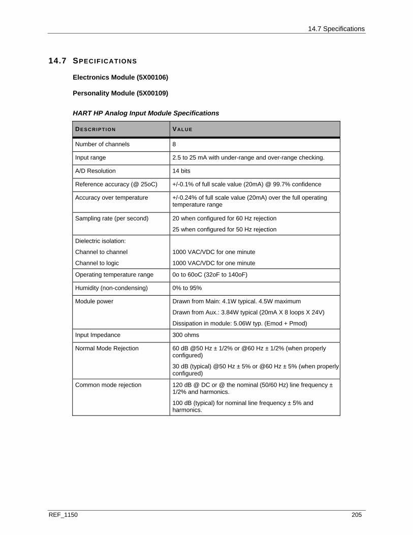
14.7 Specifications
REF_1150 205
14.7 SPECIFICATIONS
Electronics Module (5X00106)
Personality Module (5X00109)
HART HP Analog Input Module Specifications
DE S C RI P TI O N VALUE
Number of channels 8
Input range 2.5 to 25 mA with under-range and over-range checking.
A/D Resolution 14 bits
Reference accuracy (@ 25oC) +/-0.1% of full scale value (20mA) @ 99.7% confidence
Accuracy over temperature +/-0.24% of full scale value (20mA) over the full operating temperature range
Sampling rate (per second) 20 when configured for 60 Hz rejection
25 when configured for 50 Hz rejection
Dielectric isolation:
Channel to channel
Channel to logic
1000 VAC/VDC for one minute
1000 VAC/VDC for one minute
Operating temperature range 0o to 60oC (32oF to 140oF)
Humidity (non-condensing) 0% to 95%
Module power Drawn from Main: 4.1W typical. 4.5W maximum
Drawn from Aux.: 3.84W typical (20mA X 8 loops X 24V)
Dissipation in module: 5.06W typ. (Emod + Pmod)
Input Impedance 300 ohms
Normal Mode Rejection 60 dB @50 Hz ± 1/2% or @60 Hz ± 1/2% (when properly configured)
30 dB (typical) @50 Hz ± 5% or @60 Hz ± 5% (when properly configured)
Common mode rejection 120 dB @ DC or @ the nominal (50/60 Hz) line frequency ± 1/2% and harmonics.
100 dB (typical) for nominal line frequency ± 5% and harmonics.

REF_1150 207
IN THIS SECTION
Description ......................................................................................................................207 Module Group Information ..............................................................................................207 Module Specific Information............................................................................................209 Wiring Information ...........................................................................................................211 Address Location Information .........................................................................................214 Diagnostic LEDs..............................................................................................................219 Specifications ..................................................................................................................220
15.1 DESCRIPTION
The Ovation HART (Highway Addressable Remote Transducer) Analog Output Module consists of an electronic module and a personality mode. The Ovation HART Analog Output Module is designed to interface with eight HART compliant output devices utilizing a 4-20 mA control loop signal. A HART compliant output device will exchange digital information with the Ovation control system in addition to the standard 4-20 mA control loop signal. The digital information is imposed on the 4-20 mA signal according to the guidelines of the HART Protocol Specification. HART uses a low-level frequency shift-keyed sine-wave signal that is superimposed on the 4-20 mA signal. The average value of the HART signal is zero. Therefore, the HART signal does not interfere with the 4-20 mA control signal.
The HART Analog Output module is applicable for CE Mark certified systems.
Note: I/O Module General Information (see page 15) contains environmental, installation, wiring, and fuse information for I/O modules.
15.2 MODULE GROUP INFORMATION
15.2.1 ELECTRONICS MODULE (EMOD)
There is one Electronics module group for the HART Analog Output Module:
5X00062G01 contains eight multiplexed, 4-20 mA output channels that interface with eight HART output devices.
15.2.2 PERSONALITY MODULE (PMOD)
There is one Personality Module group for the HART Analog Output Module:
5X00063G01 contains passive circuitry for each of the eight channels. There is a user-serviceable fuse located on the personality module. This fuses the auxiliary power supplying the field side circuitry of the eight output channels.
S E C T I O N 1 5
HART ANALOG OUTPUT MODULE
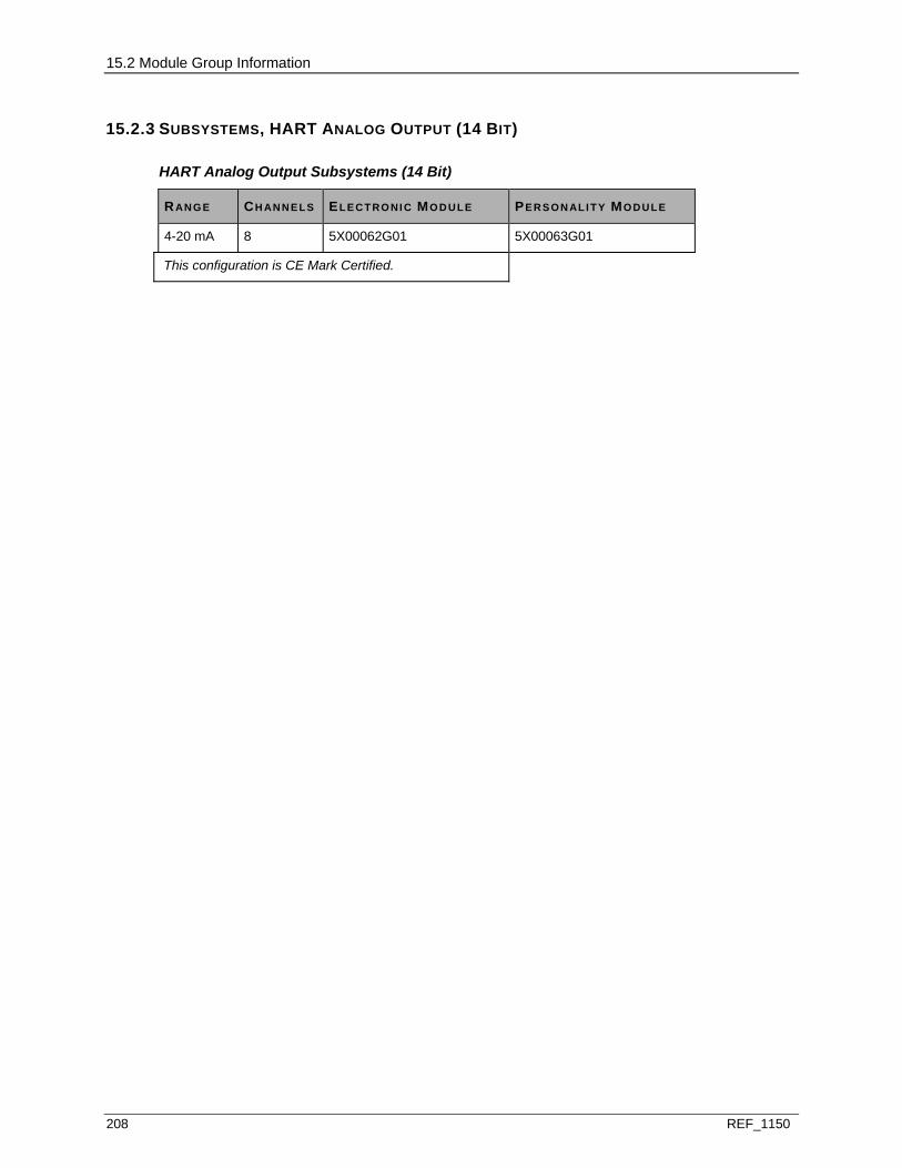
15.2 Module Group Information
208 REF_1150
15.2.3 SUBSYSTEMS, HART ANALOG OUTPUT (14 BIT)
HART Analog Output Subsystems (14 Bit)
RANG E CH AN N E L S EL E CT RO NI C MO D U LE PE R S O N AL I T Y MODULE
4-20 mA 8 5X00062G01 5X00063G01
This configuration is CE Mark Certified.
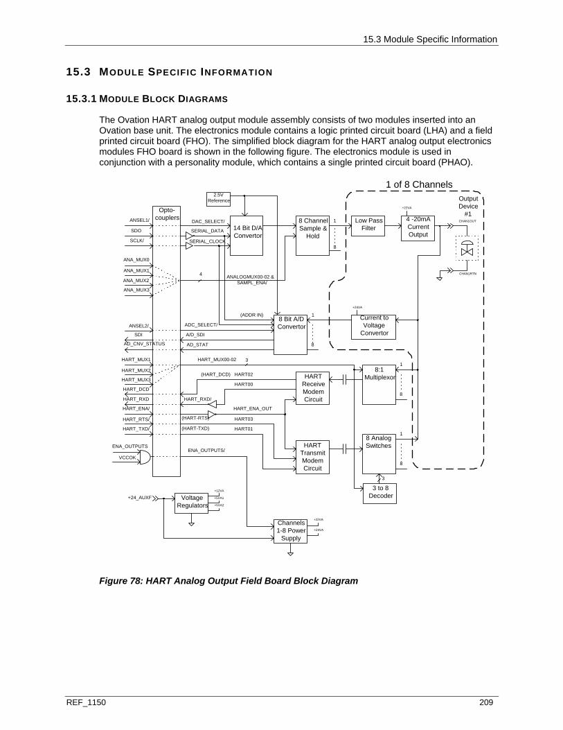
15.3 Module Specific Information
REF_1150 209
15.3 MODULE SPECIFIC INFORMATION
15.3.1 MODULE BLOCK DIAGRAMS
The Ovation HART analog output module assembly consists of two modules inserted into an Ovation base unit. The electronics module contains a logic printed circuit board (LHA) and a field printed circuit board (FHO). The simplified block diagram for the HART analog output electronics modules FHO board is shown in the following figure. The electronics module is used in conjunction with a personality module, which contains a single printed circuit board (PHAO).
ANA_MUX0
ANA_MUX1
ANA_MUX2
ANA_MUX3
HART_MUX1
HART_MUX2
HART_MUX3
HART_DCD
HART_RXD
HART_ENA/
HART_RTS/
HART_TXD/
Opto-couplersANSEL1/
SDO
SCLK/
2.5VReference
14 Bit D/AConvertor
8 ChannelSample &
Hold
4 -20mACurrentOutput
Low PassFilter
VoltageRegulators
Channels1-8 Power
Supply
HARTTransmitModemCircuit
3 to 8Decoder
8 AnalogSwitches
8:1MultiplexorHART
ReceiveModemCircuit
8 Bit A/DConvertor
Current toVoltage
Convertor
+12VA
+5VA1
+5VA2
+24_AUXF
SERIAL_DATA
SERIAL_CLOCK
DAC_SELECT/
+22VA
+24VA
OutputDevice
#1CHAN1OUT
CHAN1RTN
+22VA
ANALOGMUX00-02 &
1
8
4
(ADDR IN)
ANSEL2/
SDI
ADC_SELECT/
A/D_SDI
AD_STAT
HART_MUX00-02 3
HART_ENA_OUT
HART02
HART00
HART_RXD/
(HART_DCD)
(HART-TXD)
HART03
HART01
(HART-RTS)
ENA_OUTPUTS/
+24VA
8
1
8
1
3
8
1
1 of 8 Channels
ENA_OUTPUTS
AD_CNV_STATUS
SAMPL_ENA/
VCCOK
Figure 78: HART Analog Output Field Board Block Diagram
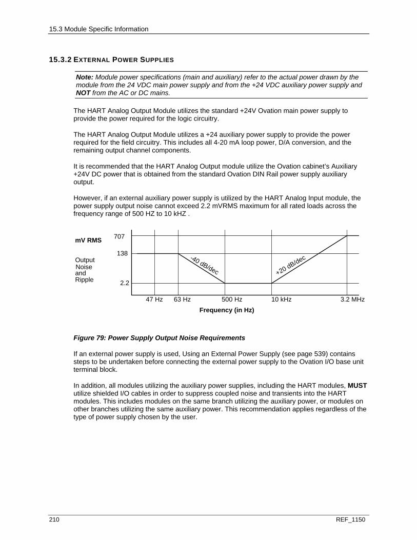
15.3 Module Specific Information
210 REF_1150
15.3.2 EXTERNAL POWER SUPPLIES
Note: Module power specifications (main and auxiliary) refer to the actual power drawn by the module from the 24 VDC main power supply and from the +24 VDC auxiliary power supply and NOT from the AC or DC mains.
The HART Analog Output Module utilizes the standard +24V Ovation main power supply to provide the power required for the logic circuitry.
The HART Analog Output Module utilizes a +24 auxiliary power supply to provide the power required for the field circuitry. This includes all 4-20 mA loop power, D/A conversion, and the remaining output channel components.
It is recommended that the HART Analog Output module utilize the Ovation cabinet’s Auxiliary +24V DC power that is obtained from the standard Ovation DIN Rail power supply auxiliary output.
However, if an external auxiliary power supply is utilized by the HART Analog Input module, the power supply output noise cannot exceed 2.2 mVRMS maximum for all rated loads across the frequency range of 500 HZ to 10 kHZ .
mV RMS
138OutputNoise and Ripple 2.2
47 Hz 63 Hz 500 Hz 10 kHz 3.2 MHz Frequency (in Hz)
707
+20 dB/dec-40 dB/dec
Figure 79: Power Supply Output Noise Requirements
If an external power supply is used, Using an External Power Supply (see page 539) contains steps to be undertaken before connecting the external power supply to the Ovation I/O base unit terminal block.
In addition, all modules utilizing the auxiliary power supplies, including the HART modules, MUST utilize shielded I/O cables in order to suppress coupled noise and transients into the HART modules. This includes modules on the same branch utilizing the auxiliary power, or modules on other branches utilizing the same auxiliary power. This recommendation applies regardless of the type of power supply chosen by the user.

15.4 Wiring Information
REF_1150 211
15.4 WIRING INFORMATION
15.4.1 HART ANALOG OUTPUT TERMINAL BLOCK WIRING INFORMATION
Each personality module has a simplified wiring diagram label on its side which appears above the terminal block. This diagram indicates how the wiring from the field is to be connected to the terminal block in the base unit. The diagrams for the HART Analog Output Personality Modules are illustrated in the following figure. The following table lists and defines the abbreviations used in those diagrams.
Figure 80: HART Analog Output Terminal Block Pin Assignments
Wiring Diagram Label Definitions
AB B R E V I AT I ON DE FI NI T I O N
A1 - A8
+
Analog Output positive terminal connection (connected to the positive terminal of a HART analog output device).
A1 - A8
-
Analog Output negative terminal connection (connected to the negative terminal of a HART analog output device)
SH1 - SH8 Shield terminal connection
Earth ground terminals
PS+, PS- External Auxiliary power supply terminals
15.4 Wiring Information
212 REF_1150
15.4.2 HART ANALOG OUTPUT FIELD CONNECTION WIRING DIAGRAMS (NON-CE MARK CERTIFIED SYSTEMS)
Pmod (PHAO)Terminal Block
sectionHART AnalogOutput EMOD
+-
A1+
PS+PS-
+ -
Auxiliary PowerSupply
HARTAnalogOutputDevices
A1-SH1
+-
4-20mA
SH2
A2+
A2-
4-20mA
To HARTReceiveModem
FromHART
TransmitModem
8
2
1
8:1Mux
8
1
2
S&HDAC
HARTAnalogOutputDevices
Auxiliary Power
Figure 81: Field Wiring (Non-CE Mark) (2 of 8 channels depicted)

15.4 Wiring Information
REF_1150 213
15.4.3 HART ANALOG OUTPUT FIELD CONNECTION WIRING DIAGRAMS (CE MARK CERTIFIED SYSTEMS)
Pmod (PHAO)Terminal Block
sectionHART AnalogOutput EMOD
+-
A1+
PS+PS-
+ -
Auxiliary PowerSupply
HARTAnalogOutputDevices
A1-SH1
+-
4-20mA
SH2
A2+
A2-
4-20mA
To HARTReceiveModem
FromHART
TransmitModem
8
2
1
8:1Mux
8
1
2
S&HDAC
NOTE: All field wiring must be braid-shielded and gorunded at the point of entry of thecabinet using the recommended hardware (refer to "Cable Guidelines" in U3-1000).
NoteAll field wiring must be braid-shielded and grounded at the point of entry of the cabinet using therecommended hardware (refer to the applicable "Cable Guidelines" information for your system).
Figure 82: Field Wiring (CE Mark) (2 of 8 channels depicted)
15.4.4 FIELD WIRING CABLE REQUIREMENTS
Field I/O cable must be one or more single-twisted pair shielded or multiple-twisted pair with overall shield. Single and multiple-pair may be combined provided that all of the shields share a common connection to earth ground in the Ovation cabinet.
Recommended Minimum Conductor Size
CABL E LE NGTH MI N. CO N D UC T O R SI ZE CABLE TY PE
Below 5,000 feet (1524 m) 24 AWG (0.51 mm dia.) Single-twisted pair shielded or multiple-twisted pair with over-all shield.
Above 5,000 (1524 m) 20 AWG (0.81 mm dia.) Single-twisted pair shielded.

15.5 Address Location Information
214 REF_1150
The maximum length of cable per HART network is dependent on the characteristics of the devices connected to the network and the characteristics of the cable to be used.
In a HART network, long cable lengths are possible when the dominant low impedance device (the HART field device) has an input impedance of approximately 250 ohms and the signal cable is good quality having low capacitance (Cx) and resistance (Rx) per unit length.
Cx = Cable capacitance per unit length (feet or meters): The capacitance from one conductor to all other conductors (including the shield if shielded). This value is usually available from the cable manufacturer.
Rx = Cable resistance per unit length (feet or meters): This value should be available from the cable manufacturer. Filed Wiring Requirements (see page 185) for the HART Analog Input Module contains the resistance values of some common copper wire sizes. The resistance per unit length is for a single wire but the length calculations and charts take into account the resistance of both wires.
Refer to field device manufacturer’s literature for more information on cabling lengths since device impedances may vary among field devices. In addition, refer to the HART FSK Physical Layer Specification (HCF_SPEC - 54) for additional information.
15.5 ADDRESS LOCATION INFORMATION
15.5.1 CONFIGURATION AND STATUS REGISTER
Word address 13 (D in Hex) is used to configure the module and provide status information to the Controller. The status register can be read by using the Point Information window at an Operator Station (see the Bit Pattern field on the Hardware tab). (See the Ovation Operator Station User Guide.)
HART Analog Output Register Map
RE G DAT A DE S C R I P T I O N - CO N FI G U R AT I O N REGI S TE R (WRI TE)
DAT A DE S C R I P T I O N - ST ATUS REGI S TER (RE AD)
0 Indirect Memory Index NA
1 Indirect Memory Data Indirect Memory Data
2 Analog Output - Channel 1 NA
3 Analog Output - Channel 2 NA
4 Analog Output - Channel 3 NA
5 Analog Output - Channel 4 NA
6 Analog Output - Channel 5 NA
7 Analog Output - Channel 6 NA
8 Analog Output - Channel 7 NA
9 Analog Output - Channel 8 NA
10 Calibration Register (Factory use only) Calibration Register (Factory use only)

15.5 Address Location Information
REF_1150 215
RE G DAT A DE S C R I P T I O N - CO N FI G U R AT I O N REGI S TE R (WRI TE)
DAT A DE S C R I P T I O N - ST ATUS REGI S TER (RE AD)
11 NA HAI Firmware Revision
12 NA Channel Error Bits
13 Module Configuration Register Module Status Register
14 NA HART Enable (See the table below)
15 Module Electronic ID Data NA
HART AO Configuration/Status Register (Address 13 or D in Hex)
BI T DAT A DE S C R I P T I O N - (WRI TE) DAT A DE S C R I P T I O N - (READ)
0 Configure Module Module Configured (1 = configured; 0 = unconfigured)
1 Force Error Internal or forced error (1 = forced error; 0 = no forced error)
2 - 4 Communications Timeout Setting 1
BI T 4
BI T 3
BI T 2
T I M EO U T
0 0 0 16 seconds
0 0 1 4 seconds
0 1 0 2 seconds
0 1 1 1 seconds
1 0 0 500 milliseconds
1 0 1 250 milliseconds
1 1 0 125 milliseconds
1 1 1 62.5 milliseconds
Communications Timeout Setting 1
BI T 4
BI T 3
BI T 2
T I M EO U T
0 0 0 16 seconds
0 0 1 4 seconds
0 1 0 2 seconds
0 1 1 1 seconds
1 0 0 500 milliseconds
1 0 1 250 milliseconds
1 1 0 125 milliseconds
1 1 1 62.5 milliseconds 5 Timeout Action NA
6 Reserved for Factory Test (must always be set to 0) NA
7 Reserved for Factory Test (must always be set to 0) NA
8 NA Hardware Error
9 Not Used Not Used
10 Not Used Not Used
11 Not Used Not Used
12 Not Used Not Used
13 Not Used Not Used
14 NA Field Power Failed

15.5 Address Location Information
216 REF_1150
BI T DAT A DE S C R I P T I O N - (WRI TE) DAT A DE S C R I P T I O N - (READ)
15 Reserved Reserved
1 The tolerance on the timeout period is +/- 35%.
Bit definitions for this register are encoded as shown above and described below:
Bit 0: Configures the module (write) or indicates the configuration state of the module (read). A “1” indicates that the module is configured. Until the module is configured, addresses 0 through 11 will produce an attention status.
Bit 1: This bit (write “1”) forces the module into its error state causing the Internal Error LED to light.
Bits 2-4: These bits are used to select the Controller communications timeout period.
Bit 5: If this bit is set and the Controller times out, the module will continue to output the last value received. If the bit is cleared and the Controller times out, the module will output zero to the DAC for each channel, yielding 0 mA on the outputs after the time out period defined by bits 2-4.
Bits 6-7: Reserved for use by the Factory Test. These bits must always be set to 0.
Bit 8: When set, this indicates one or more of the following conditions are true:
- The FPGA did not program correctly upon startup. - The EE memory checksum is incorrect. - The PROM checksum test has failed. - Internal memory diagnostic has failed.
Bits 9-13: Not Used.
Bit 14: Field power failed.
Bit 15: Reserved.
HART Analog Output Enable Register (Address 14 or E in Hex)
BI T DAT A DE S C R I P T I O N - CO NF I G U R AT I O N RE GI S T E R (WRI T E)
DAT A DE S C R I P T I O N - ST ATUS RE GI S T E R (RE AD)
0 Multi-variable Enabled NA
1 Multi-variable Enabled NA
2 Multi-variable Enabled NA
3 Multi-variable Enabled NA
4 Multi-variable Enabled NA
5 Multi-variable Enabled NA
6 Multi-variable Enabled NA
7 Multi-variable Enabled NA
8 HART Enabled - Channel 1 NA
9 HART Enabled - Channel 2 NA
15.5 Address Location Information
REF_1150 217
BI T DAT A DE S C R I P T I O N - CO NF I G U R AT I O N RE GI S T E R (WRI T E)
DAT A DE S C R I P T I O N - ST ATUS RE GI S T E R (RE AD)
10 HART Enabled - Channel 3 NA
11 HART Enabled - Channel 4 NA
12 HART Enabled - Channel 5 NA
13 HART Enabled - Channel 6 NA
14 HART Enabled - Channel 7 NA
15 HART Enabled - Channel 8 NA
Bits 0-7: These bits are set to enable multivariable messaging.
The HAI, HAO, HART High Performance AI and HART High Performance AO modules have the ability to retrieve additional variables from a field device. These variables are referred to as ‘multivariables’ and are named PV (primary variable), SV (secondary variable), TV (tertiary variable), and QV (quarterly variable).
If the bit is set, the module will periodically retrieve whatever variables exist for the device.
The definitions of PV, SV, TV, and QV are found in the user’s manual for the field device supplied by the device manufacturer. The standard format of these four variables is IEEE 794, a floating-point format.
You must configure IO point records to cause the Controller to scan the module and retrieve the variables. (See the Ovation Point Builder User Guide or Ovation Developer Studio User Guide.).
Bits 8-15: In the IO configuration tool, you can set these flags on a per-channel basis to allow HART messaging, including Multivariable messaging, to flow on that channel.
15.5.2 OPEN LOOP DETECT REGISTER
If one of these bits is set, the channel readback diagnostic indicates the difference between the desired value and the actual value exceeds the accepted deadband. This bit signifies an open loop condition.
Pass/Fail per Channel Register (Address 12 or C in Hex)
BI T DAT A DE S C R I P T I O N - CO NF I G U R AT I O N RE GI S T E R (WRI T E)
DAT A DE S C R I P T I O N - ST ATUS RE GI S T E R (RE AD)
0 NA Channel 1 bad
1 NA Channel 2 bad
2 NA Channel 3 bad
3 NA Channel 4 bad
4 NA Channel 5 bad
5 NA Channel 6 bad
6 NA Channel 7 bad

15.5 Address Location Information
218 REF_1150
BI T DAT A DE S C R I P T I O N - CO NF I G U R AT I O N RE GI S T E R (WRI T E)
DAT A DE S C R I P T I O N - ST ATUS RE GI S T E R (RE AD)
7 NA Channel 8 bad
8 Not Used Not Used
9 Not Used Not Used
10 Not Used Not Used
11 Not Used Not Used
12 Not Used Not Used
13 Not Used Not Used
14 Not Used Not Used
15 Not Used Not Used
HART Analog Output Enable Register (Address 14 or E in Hex)
BI T DAT A DE S C R I P T I O N - CO NF I G U R AT I O N RE GI S T E R (WRI T E)
DAT A DE S C R I P T I O N - ST ATUS RE GI S T E R (RE AD)
0 Multi-variable Enabled - Channel 1 Not used
1 Multi-variable Enabled - Channel 2 Not used
2 Multi-variable Enabled - Channel 3 Not used
3 Multi-variable Enabled - Channel 4 Not used
4 Not used Not used
5 Not used Not used
6 Not used Not used
7 Not used Not used
8 HART Enabled - Channel 1 Not used
9 HART Enabled - Channel 2 Not used
10 HART Enabled - Channel 3 Not used
11 HART Enabled - Channel 4 Not used
12 Not used Not used
13 Not used Not used
14 Not used Not used
15 Not used Not used
Bit definitions for this register are encoded as shown above and described below:
Bits 0-3:These bits in the Configuration Register are set to enable multivariable messaging.

15.6 Diagnostic LEDs
REF_1150 219
The LOH module has the ability to retrieve additional variables from a field device. These variables are referred to as ‘multivariables’ and are named PV (primary variable), SV (secondary variable), TV (tertiary variable), and QV (quarterly variable).
If the bit is set, the module will periodically retrieve whatever variables exist for the device.
The definitions of PV, SV, TV, and QV are found in the user’s manual for the field device supplied by the device manufacturer. The standard format of these four variables is IEEE 794, a floating-point format.
You must configure IO point records to cause the Controller to scan the module and retrieve the variables. For additional information refer to the applicable Ovation Point Builder User Guide for your system.
Bits 4 - 7: Not used.
Bits 8-15: A “1” in any of these bits in the Status Register indicate that a HART compliant device exists on the corresponding channel.
You should ensure that these bits are cleared for non-HART field devices. To avoid a HART communication error message, set each bit at “0” when connecting a non-HART output device.
15.6 DIAGNOSTIC LEDS
The following table lists the module’s LEDs and describes what they mean when lit.
HART Analog Output LEDs
LED DE S C RI P TI O N
P (Green) Power OK LED. Illuminated when the +5V power is OK.
C (Green) Communications OK LED. Illuminated when the Controller is communicating with the module.
E (Red) External Error LED. Illuminated upon loss of external auxiliary (field) power, as indicated by the loss of normal transitions of the EOC (end-of-convert) signal.
I (Red) Internal Error LED. Illuminated whenever there is any type of error within the module except for a loss of external auxiliary power. Possible causes are:
- The Controller sets the module’s Force Error bit.
- Communications with the Controller is lost.
- EPROM, EE memory or RAM diagnostic failure.

15.7 Specifications
220 REF_1150
LED DE S C RI P TI O N
1-8 (Green) After module configuration, the bank of eight channel LEDs (LEDs 1 through 8) is used to indicate HART communication activity. When a HART message is sent, the LED for that particular channel is illuminated. When the HART response is received correctly, the LED is extinguished. Therefore, when all is normal, that is, messages and responses are properly exchanged, a single LED blink will be observed on the module’s front cap.
If a HART message is sent and no response is received, the HART Analog Output module exclusive-OR’s the channel LED display with hex code 0xFF. This results in all channel LEDs being illuminated except for the selected channel. For example, if the HART Analog Output module sent a HART message to a device on channel 2, but the device was not connected to channel 2, the module would first illuminate LED 2 (all seven other channel LEDs extinguished). The module would then extinguish LED 2 and flash the other seven channel LEDs. This status indicates that the module sent a HART message on channel 2 and did not receive a valid response message after the initial message attempt or after any of the subsequent message retries.
15.7 SPECIFICATIONS
Electronics Module (5X00062)
Personality Module (5X00063)
HART Analog Output Channel Specifications
DE S C RI P TI O N VALUE
Number of channels 8
Channel Update Rate 24 mS (Each channel is updated once every 24 mS by the on-board microcontroller, 14 Bit resolution typ.)
Output Range 4 to 20 mA
D/A Resolution 14 Bits
Accuracy over Temperature Range 0.25% of Span
User Loop Voltage Power for loop current is supplied through the module by an auxiliary power supply.
Diagnostics Open loop feedback detection. 8 Pass/Fail bits are stored in data register 0xC in Hex.
Dielectric isolation:
Channel to Channel
Channel to logic
None
1000 VAC/VDC for 1 minute.
Output Loading 4-20 mA into 700 ohm load maximum (230 ohm minimum to 600 ohm maximum).1
Output Compliance 20 [email protected] VDC Supply into 700 ohm load.

15.7 Specifications
REF_1150 221
DE S C RI P TI O N VALUE
Operating Temperature Range 0o to 60o C
Humidity (non-condensing) 0% to 95%
Module Power Main: 24 VDC
1.2 W typical, 2.5W maximum
Aux: 24 VDC (-5%,+6.25%)
6W typical, 7.2W maximum 1 Per the HART Physical Layer Specification (HCF_SPEC - 54).

REF_1150 223
IN THIS SECTION
Description ......................................................................................................................223 Module Group Information ..............................................................................................223 Module Specific Information............................................................................................225 Wiring Information ...........................................................................................................226 Address Location Information .........................................................................................229 Diagnostic LEDs..............................................................................................................233 Specifications ..................................................................................................................234
16.1 DESCRIPTION
The Ovation HART High Performance Analog Output Module consists of an electronic module and a personality mode cavity insert. The Ovation HART High Performance Analog Output Module is designed to interface with four HART compliant output devices utilizing a 4-20 mA control loop signal. A HART compliant output device will exchange digital information with the Ovation control system in addition to the standard 4-20 mA control loop signal. The digital information is imposed on the 4-20 mA signal according to the guidelines of the HART Protocol Specification. HART uses a low-level frequency shift-keyed sine-wave signal that is superimposed on the 4-20 mA signal. The average value of the HART signal is zero. Therefore, the HART signal does not interfere with the 4-20 mA control signal.
Note: I/O Module General Information (see page 15) contains environmental, installation, wiring, and fuse information for I/O modules.
16.2 MODULE GROUP INFORMATION
16.2.1 ELECTRONICS MODULE (EMOD)
There is one Electronics module group for the HART High Performance Analog Output Module:
5X00167G01 contains four independent self-powered, 4-20 mA output channels that interface with 4 HART output devices.
16.2.2 SUBSYSTEMS, HART ANALOG OUTPUT (16 BIT)
HART Analog Output Subsystems (16 Bit)
SP AN CH AN N E L S EL E CT RO NI C MO D U LE PE R S O N AL I T Y MODULE
4-20 mA 4 5X00167G01 Cavity Insert 1X00188H01
S E C T I O N 1 6
HART HIGH PERFORMANCE ANALOG OUTPUT MODULE

16.2 Module Group Information
224 REF_1150
A personality module is not required in order to use the HART High Performance Analog Output module. However, there may be requirements to use the Ovation Analog Output module base unit terminal assignments for the actuator interface field wiring. In those cases, the 5X00170G01 HART High Performance Analog Output personality module must be used.
16.3 Module Specific Information
REF_1150 225
16.3 MODULE SPECIFIC INFORMATION
16.3.1 MODULE BLOCK DIAGRAMS
The Ovation HART High Performance Analog Output module assembly consists of one module inserted into an Ovation base unit. The electronics module contains a logic printed circuit board (LOH) and a field printed circuit board (FOH). The simplified block diagram for the HART High Performance Analog Output electronics modules FOH board is shown in the following two figures. The electronics module is used in conjunction with a personality module cavity insert which plugs into the base unit cavity normally occupied by a personality module.
A
CurrentRegulatorControlCircuit
HARTSignal
ReceiveFilter
A
H
VoltageRegulators
A
H
VDD
+1.23V
LoopCurrent
MagnitudeMonitor
A
HARTModem
MODAC3
AH
DAC Output+1.23V
HART Output
HART Input
+3.1V-I
CurrentSense
Resistor
-+
HI
VoltageRegulator
+4.7V
VI
OpticalCouplers
LO_LIM/
HI_LIM/
ClockRecovery921.6 KHz
I
CLK_921_6KHZ
RTS & TX2
2 RX & CD/
3SPI Bus Signals
IDCLK/, IDATA/ & ICS/
IKICK/
(Watchdog TimerPulse signal)
+I
VCC
I
+24V
ExternalActuator
ILoop
Is
Is
I
I
ILoop
I
2
2
3
+24V
VCC
FOH Field Board Analog OutputChannel (One of Four)
Logic BoardConnector
I
VI
Figure 83: HART High Performance Analog Output Field Board Block Diagram (with 1X00188H01 Personality Module Cavity Foam Insert Present)

16.4 Wiring Information
226 REF_1150
Figure 84: HART High Performance Analog Output Field Board Block Diagram (5X00170G01 Personality Module Present)
16.4 WIRING INFORMATION
16.4.1 OUTPUT TERMINAL BLOCK WIRING INFORMATION
Each personality module cavity insert has a simplified wiring diagram label on its top which appears above the terminal block. This diagram indicates how the wiring from the field is to be connected to the terminal block in the base unit. The wiring diagrams for the HART High Performance Analog Output Personality Modules are illustrated in HART Analog Output Field Connection Wiring Diagrams.
Abbreviations Used in Diagrams
AB B R E V I AT I ON DE FI NI T I O N
+I Analog Output positive terminal connection (connected to the positive terminal of a HART analog output device).
-I Analog Output negative terminal connection (connected to the negative terminal of a HART analog output device)
Earth ground terminals
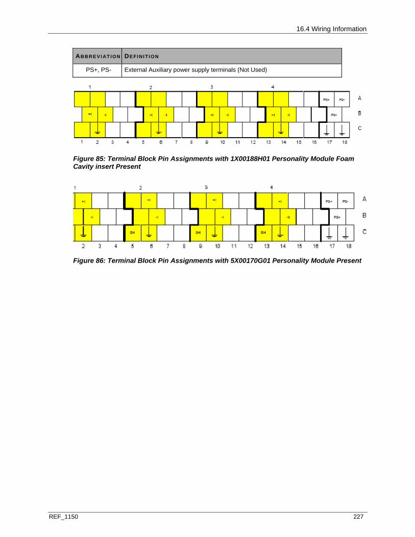
16.4 Wiring Information
REF_1150 227
AB B R E V I AT I ON DE FI NI T I O N
PS+, PS- External Auxiliary power supply terminals (Not Used)
Figure 85: Terminal Block Pin Assignments with 1X00188H01 Personality Module Foam Cavity insert Present
Figure 86: Terminal Block Pin Assignments with 5X00170G01 Personality Module Present
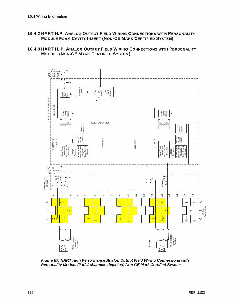
16.4 Wiring Information
228 REF_1150
16.4.2 HART H.P. ANALOG OUTPUT FIELD WIRING CONNECTIONS WITH PERSONALITY MODULE FOAM CAVITY INSERT (NON-CE MARK CERTIFIED SYSTEM)
16.4.3 HART H. P. ANALOG OUTPUT FIELD WIRING CONNECTIONS WITH PERSONALITY MODULE (NON-CE MARK CERTIFIED SYSTEM)
PS+ PS-
PS+
AB
C
-I -I -I
+I
-I
+I +I +I
6 7 8 9 10 11 12 13 14 15 16 181 2 4 53
I/O B
ase
Term
inat
ions
AB
C
HA
RT
Com
patib
le
Actu
ator
or
Pos
ition
er
HA
RT
Com
patib
le
Act
uato
r or
Posi
tione
r
17
Ear
th G
nd(C
2)
+I (A
2)
-I (B
2)
24V AUXAUX RETURNEARTH
Loop
Pow
er
Supp
ly a
nd
MO
DA
C C
lock
R
ecov
ery
Volta
ge
Reg
ulat
ors
HA
RT
Sign
al
Rcv
. & C
urre
nt
Reg
ulat
orLo
op C
urre
nt
Mon
itor
MO
DA
C3
HA
RT
Mod
emO
ptic
alIs
olat
ors
CH
ANN
EL 1
ISOLATION BARRIER
Loop
Pow
er
Supp
ly a
nd
MO
DA
C C
lock
R
ecov
ery
Volta
ge
Reg
ulat
ors
HA
RT
Sign
al
Rcv
. & C
urre
nt
Reg
ulat
orLo
op C
urre
nt
Mon
itor
MO
DA
C3
HA
RT
Mod
em
CH
ANN
EL 4
CH
AN
NEL
2
+I (A
14)
-I (B
14)
CH
AN
NEL
3
Pow
er
Sup
ply
Driv
ers
Pow
er
Sup
ply
Driv
ers
Opt
ical
Isol
ator
s
Logi
c P
ower
S
uppl
y
Pro
cess
or
Circ
uit
CP
LD
I/O
Inte
rface
Fiel
d C
ard
Inte
rface
24V MAIN (A)24V MAIN (B)MAIN RETURNI/O BUS
ELE
CTR
ON
ICS
MO
DU
LE
SH SH SH SH
PER
SO
NA
LITY
MO
DU
LE
LOG
IC C
AR
DFI
ELD
CAR
D
Figure 87: HART High Performance Analog Output Field Wiring Connections with Personality Module (2 of 4 channels depicted) Non-CE Mark Certified System

16.5 Address Location Information
REF_1150 229
16.4.4 FIELD WIRING CABLE REQUIREMENTS
Field I/O cable must be one or more single-twisted pair shielded or multiple-twisted pair with overall shield. Single and multiple-pair may be combined provided that all of the shields share a common connection to earth ground in the Ovation cabinet.
Recommended Minimum Conductor Size
CABL E LE NGTH MI N. CO N D UC T O R SI ZE CABLE TY PE
Below 5,000 feet (1524 m) 24 AWG (0.51 mm dia.) Single-twisted pair shielded or multiple-twisted pair with over-all shield.
Above 5,000 (1524 m) 20 AWG (0.81 mm dia.) Single-twisted pair shielded.
The maximum length of cable per HART network is dependent on the characteristics of the devices connected to the network and the characteristics of the cable to be used.
16.5 ADDRESS LOCATION INFORMATION
16.5.1 HART HIGH PERFORMANCE ANALOG OUTPUT MODULE REGISTERS
HART Analog Output Register Map
RE G DAT A DE S C R I P T I O N - CO NF I G U R AT I O N RE GI S T E R (WRI T E)
DAT A DE S C R I P T I O N - ST ATUS RE GI S T E R (RE AD)
0 Indirect Memory Index NA
1 Indirect Memory Data Indirect Memory Data
2 Analog Output - Channel 1 NA
3 Analog Output - Channel 2 NA
4 Analog Output - Channel 3 NA
5 Analog Output - Channel 4 NA
6 Not Used Not Used
7 Not Used Not Used
8 Not Used Not Used
9 Not Used Not used
10 Reserved Reserved
11 NA LOH Firmware Revision
12 NA Channel Error Bits
13 Module Configuration Register Module Status Register
14 NA Multivariable Enable/HART Enable

16.5 Address Location Information
230 REF_1150
RE G DAT A DE S C R I P T I O N - CO NF I G U R AT I O N RE GI S T E R (WRI T E)
DAT A DE S C R I P T I O N - ST ATUS RE GI S T E R (RE AD)
15 Module Electronic ID Data NA
Configuration and Status Register
Word address 13 (D in Hex) is used to write to the Module Configuration Register and to read the Module Status Register. The status register can be read by using the Point Information window at an Operator Station (see the Bit Pattern field on the Hardware tab). (See the Ovation Operator Station User Guide.)
Configuration/Status Register (Address 13 or D in Hex)
BI T DAT A DE S C R I P T I O N - (WRI TE)
DAT A DE S C R I P T I O N - (READ)
0 Configure Module Module Configured (1 = configured; 0 = unconfigured)
1 Force Error Internal or forced error (1 = forced error; 0 = no forced error)
2 Communication Timeout bit 0 NA
3 Communication Timeout bit 1 NA
4 Communication Timeout bit 2 NA
5 Timeout Action NA
6 Factory Test Not Used
7 Reserved Reserved
8 NA Channel 1 - over-under
9 NA Channel 2 - over-under
10 NA Channel 3 - over-under
11 NA Channel 4 - over-under
12 Not Used Not Used
13 Not Used Not Used
14 Not Used Not Used
15 Not Used Not Used
Bit 0: Configures the module (write) or indicates the configuration state of the module (read). “1” indicates that the module is configured. Until module is configured, addresses 0 through 11 will produce an attention status.
Bit 1: This bit (write “1”) forces the module into its error state causing the Internal Error LED to light.
Bits 2-4: These bits are used to select the Controller communications timeout period.
16.5 Address Location Information
REF_1150 231
Bit 5: If this bit is set and the Controller times out, the module will continue to output the last value received. If the bit is cleared and the Controller times out, the module will output data to the DAC for each channel, that yields 4mA on the outputs after the time-out period defined by bits 2-4.
Bit 6: This bit is only used in the manufacturing test. When the bit is set and PE is active, the module enters a factory test mode.
Bits 7: Reserved.
Bit 8: 1=Channel 1 output current is overrange or underrange.
Bit 9: 1=Channel 2 output current is overrange or underrange.
Bit 10: 1=Channel 3 output current is overrange or underrange.
Bit 11: 1=Channel 4 output current is overrange or underrange.
Bits 12-15: Not Used.
Output Communication Timeout Settings
TI M EO U T BI T 2 T I M EO U T BI T 1 T I M EO U T BI T 0 T I M EO U T PE RI O D
0 0 0 16 seconds
0 0 1 4 seconds
0 1 0 2 seconds
0 1 1 1 second
1 0 0 500 milliseconds
1 0 1 250 milliseconds
1 1 0 125 milliseconds
1 1 1 62 milliseconds
Time-outs have a tolerance of +/- 35%. The default after a power-up is 16 seconds is.
Channel Error Bit
The following table is for reference only, Individual bits are not user accessible.
Over/Under Current Limit Register (Address 12 or C in Hex)
BI T DAT A DE S C R I P T I O N - CO N FI G U R AT I O N REGI S TE R (WRI TE)
DAT A DE S C R I P T I O N - ST ATUS RE GI S T E R (RE AD)
0 NA Channel 1 Under Current
1 NA Channel 2 Under Current
2 NA Channel 3 Under Current
3 NA Channel 4 Under Current
4 NA Channel 1 Over Current
16.5 Address Location Information
232 REF_1150
BI T DAT A DE S C R I P T I O N - CO N FI G U R AT I O N REGI S TE R (WRI TE)
DAT A DE S C R I P T I O N - ST ATUS RE GI S T E R (RE AD)
5 NA Channel 2 Over Current
6 NA Channel 3 Over Current
7 NA Channel 4 Over Current
8 Not Used Not Used
9 Not Used Not Used
10 Not Used Not Used
11 Not Used Not Used
12 Not Used Not Used
13 Not Used Not Used
14 Not Used Not Used
15 Not Used Not Used
Enable Register (Address 14 or E in Hex)
BI T DAT A DE S C R I P T I O N - CO NF I G U R AT I O N RE GI S T E R (WRI T E)
DAT A DE S C R I P T I O N - ST ATUS RE GI S T E R (RE AD)
0 Multi-variable Enabled - Channel 1 NA
1 Multi-variable Enabled - Channel 2 NA
2 Multi-variable Enabled - Channel 3 NA
3 Multi-variable Enabled - Channel 4 NA
4 Not Used Not Used
5 Not Used Not Used
6 Not Used Not Used
7 Not Used Not Used
8 HART Enabled - Channel 1 NA
9 HART Enabled - Channel 2 NA
10 HART Enabled - Channel 3 NA
11 HART Enabled - Channel 4 NA
12 Not Used Not Used
13 Not Used Not Used
14 Not Used Not Used
15 Not Used Not Used

16.6 Diagnostic LEDs
REF_1150 233
Bits 0-3: These bits are set to enable multivariable messaging. Refer to the IO configuration guide for additional information.
The HAI, HAO, HART High Performance AI, HART High Performance AO modules have the ability to retrieve additional variables from a field device. These variables are referred to as ‘multivariables’ and are named PV (primary variable), SV (secondary variable), TV (tertiary variable), and QV (quarterly variable).
If the bit is set, the module will periodically retrieve whatever variables exist for the device.
The definitions of PV, SV, TV, and QV are found in the user’s manual for the field device supplied by the device manufacturer. The standard format of these four variables is IEEE 794, a floating-point format.
You must configure IO point records to cause the Controller to scan the module and retrieve the variables. (See Ovation Point Builder or Ovation Developer Studio User Guide.)
Bits 8-11: In the IO configuration tool, you can set these flags on a per-channel basis to allow HART messaging, including Multivariable messaging, to flow on that channel.
You should ensure that these bits are cleared for non-HART field devices. To avoid a HART communication error message, set each bit at “0” when connecting a non-HART output device.
16.6 DIAGNOSTIC LEDS
The following table lists the module’s LEDs and describes what they mean when lit.
HART High Performance Analog Output LEDs
LED DE S C RI P TI O N
P (Green) Power OK LED. Illuminated when the +5V power is OK.
C (Green) Communications OK LED. Illuminated when the Controller is communicating with the module.
I (Red) Internal Error LED. Illuminated whenever there is any type of error within the module except for a loss of external auxiliary power. Possible causes are:
- The Controller sets the module’s Force Error bit.
- Communications with the Controller is lost.
- Flash Memory, EE memory or RAM diagnostic failure.
1-4 (Green) After module configuration, the bank of four channel LEDs (LEDs 1 through 4) is used to indicate HART communication activity and the health of the analog outputs. If the analog output for the associated analog output channel is healthy (no overcurrent or undercurrent condition), then the channel LED will be ON. If the analog output channel is bad (an overcurrent or undercurrent is present), then the channel LED will be off.
When a HART message is sent and received correctly, the channel LED will blink off for 100 msec if the analog output is healthy. When a HART message is sent and received incorrectly, the channel LED will blink off for 400 msec if the analog output is healthy.
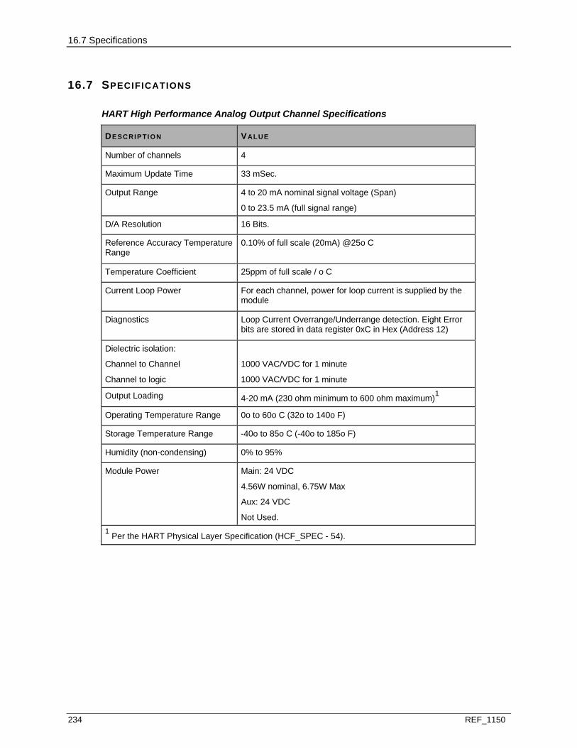
16.7 Specifications
234 REF_1150
16.7 SPECIFICATIONS
HART High Performance Analog Output Channel Specifications
DE S C RI P TI O N VALUE
Number of channels 4
Maximum Update Time 33 mSec.
Output Range 4 to 20 mA nominal signal voltage (Span)
0 to 23.5 mA (full signal range)
D/A Resolution 16 Bits.
Reference Accuracy Temperature Range
0.10% of full scale (20mA) @25o C
Temperature Coefficient 25ppm of full scale / o C
Current Loop Power For each channel, power for loop current is supplied by the module
Diagnostics Loop Current Overrange/Underrange detection. Eight Error bits are stored in data register 0xC in Hex (Address 12)
Dielectric isolation:
Channel to Channel
Channel to logic
1000 VAC/VDC for 1 minute
1000 VAC/VDC for 1 minute
Output Loading 4-20 mA (230 ohm minimum to 600 ohm maximum)1
Operating Temperature Range 0o to 60o C (32o to 140o F)
Storage Temperature Range -40o to 85o C (-40o to 185o F)
Humidity (non-condensing) 0% to 95%
Module Power Main: 24 VDC
4.56W nominal, 6.75W Max
Aux: 24 VDC
Not Used. 1 Per the HART Physical Layer Specification (HCF_SPEC - 54).
REF_1150 235
IN THIS SECTION
Description ......................................................................................................................235 Module Group Information ..............................................................................................235
17.1 DESCRIPTION
The Link Controller (LC) module provides the Ovation Controller with a serial data communications link to a third-party device or system. This communication is done via a serial RS-232, RS-422, or RS-485 data link. Two serial ports are provided.
This module is not described in this document. (See Ovation LC Module Interface User Guide.)
The Link Controller Module is applicable for CE Mark Certified Systems.
Note: I/O Module General Information (see page 15) contains environmental, installation, wiring, and fuse information for I/O modules.
17.2 MODULE GROUP INFORMATION
17.2.1 ELECTRONICS MODULE (EMOD)
There is one Electronics module group for the Link Controller Module:
1C31166G01 provides for communication to a third-party device or system.
17.2.2 PERSONALITY MODULES (PMODS)
There are two Personality module groups for the Link Controller Module:
1C31169G01 provides for an RS-232 serial link (in CE Mark certified systems, the application port cable must be less than 10 meters (32.8 ft)).
1C31169G02 provides for an RS-485 serial link (also may be used to provide for an RS-422 serial link).
S E C T I O N 1 7
LINK CONTROLLER (LC) MODULE
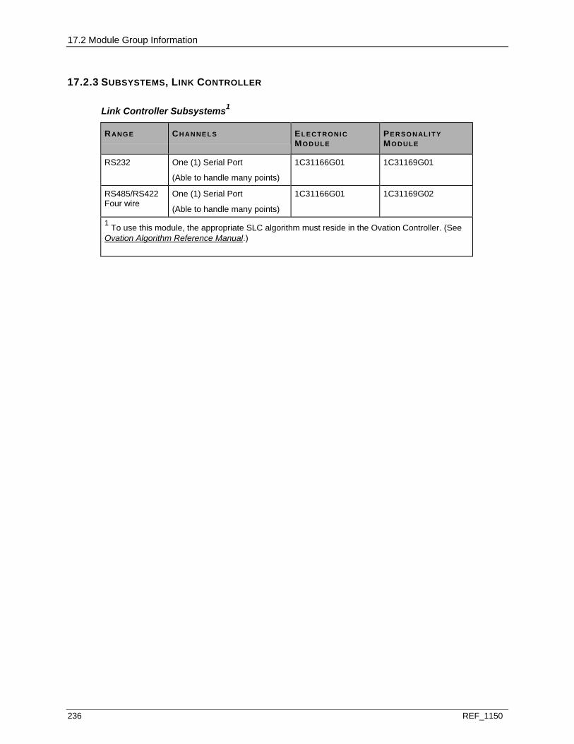
17.2 Module Group Information
236 REF_1150
17.2.3 SUBSYSTEMS, LINK CONTROLLER
Link Controller Subsystems1
RANG E CH AN N E L S EL E CT RO NI C MO D U LE
PE R S O N AL I T Y MO D U LE
RS232 One (1) Serial Port
(Able to handle many points)
1C31166G01 1C31169G01
RS485/RS422 Four wire
One (1) Serial Port
(Able to handle many points)
1C31166G01 1C31169G02
1 To use this module, the appropriate SLC algorithm must reside in the Ovation Controller. (See Ovation Algorithm Reference Manual.)

REF_1150 237
IN THIS SECTION
Description ......................................................................................................................237 Module Group Information ..............................................................................................238 Module Specific Information............................................................................................241 Wiring Information ...........................................................................................................243 Address Location Information .........................................................................................260 Diagnostic LEDs..............................................................................................................262 Specifications ..................................................................................................................264
18.1 DESCRIPTION
The Ovation single-loop Controller is designed to interface to the analog and digital I/O necessary to control a single process loop. In addition, the Ovation single-loop Controller displays this process information and provides for manual control via a local operator interface station.
The Ovation single-loop interface module provides the following field inputs and outputs necessary to interface to a single loop:
Two individually isolated analog inputs. One isolated analog output. Two individually isolated digital inputs. Two isolated digital outputs (the outputs share a common ground with each other, but are
isolated from the other I/O circuits and from the logic portion of the module).
In addition, the single-loop interface module contains an RS-422 serial port for communications with a loop interface module (SLIM) and an interface for communications over the Ovation serial I/O bus.
The Loop Interface Module is applicable for CE Mark Certified Systems.
Note: I/O Module General Information (see page 15) contains environmental, installation, wiring, and fuse information for I/O modules.
S E C T I O N 1 8
LOOP INTERFACE MODULE
18.2 Module Group Information
238 REF_1150
18.2 MODULE GROUP INFORMATION
18.2.1 MODULE GROUPS
There are two basic styles of single-loop interface modules, Normal (non-electric drive) and Electric Drive:
Normal (non-electric drive) Type - This type of module calculates the process variable for display at the SLIM by converting analog input 1 to engineering units. The output to the field is the analog output. This type of module may use a group 1, 2, or 3 Electronics module.
Electric Drive Type - Two types of Electric Drive modes are supported. Electric Drive module types are available with group 4 Electronics modules only. The mode of the Electric Drive is controlled through software.
Electric Drive Type (Mode 1) This type of module calculates the process variable from analog input 1, and the output (Demand) is calculated by the Controller as in Normal (non-electric drive) card styles. However, the output to the field are the two digital outputs. The output (Demand) from the Controller is compared to the process position (analog input 2), and raise and output pulses are generated accordingly to control the process. Digital output 1 corresponds to raise and digital output 2 corresponds to lower. The outputs are pulsed with the duty cycle proportional to the speed of the raise or lower action. The raise/lower ON/OFF times are specified in the control algorithm.
Electric Drive Type (Mode 2) As in Electric Drive (Mode 1), this type of module calculates the process variable from analog input 1, and its field output are two digital outputs. However, in all operating modes except Local, a demand of zero (0) will force a hard (non-pulsing) lower. This means that digital output 2 will be forced active LOW and will remain LOW until the demand is not equal to 0. Local mode operation is unchanged.
18.2.2 ELECTRONIC MODULES (EMODS)
There are four groups of Electronics modules for the Loop Interface Module:
1C31174G01 provides analog inputs 0 to +10V, and analog outputs 0 to +10V, digital inputs 24/48 VDC and digital outputs 60 VDC.
1C31174G02 provides analog inputs 0 to +5V, and analog outputs 0 to +10V, digital inputs 24/48 VDC and digital outputs 60 VDC.
1C31174G03 provides analog inputs 4 to 20mA, and analog outputs 4 to 20mA, digital inputs 24/48 VDC and digital outputs 60 VDC.
1C31174G04 provides analog inputs 4 to 20mA, and no analog output (Electric Drive), digital inputs 24/48 VDC and digital outputs 60 VDC.
18.2.3 PERSONALITY MODULES (PMODS)
There are three groups of Personality modules for the Loop Interface Module:
1C31177G01 provides voltage analog inputs and configurable remote or local shield grounding.
1C31177G02 provides current analog inputs and locally powered, local shield grounding. 1C31177G03 provides current analog inputs and field powered, remote shield grounding.
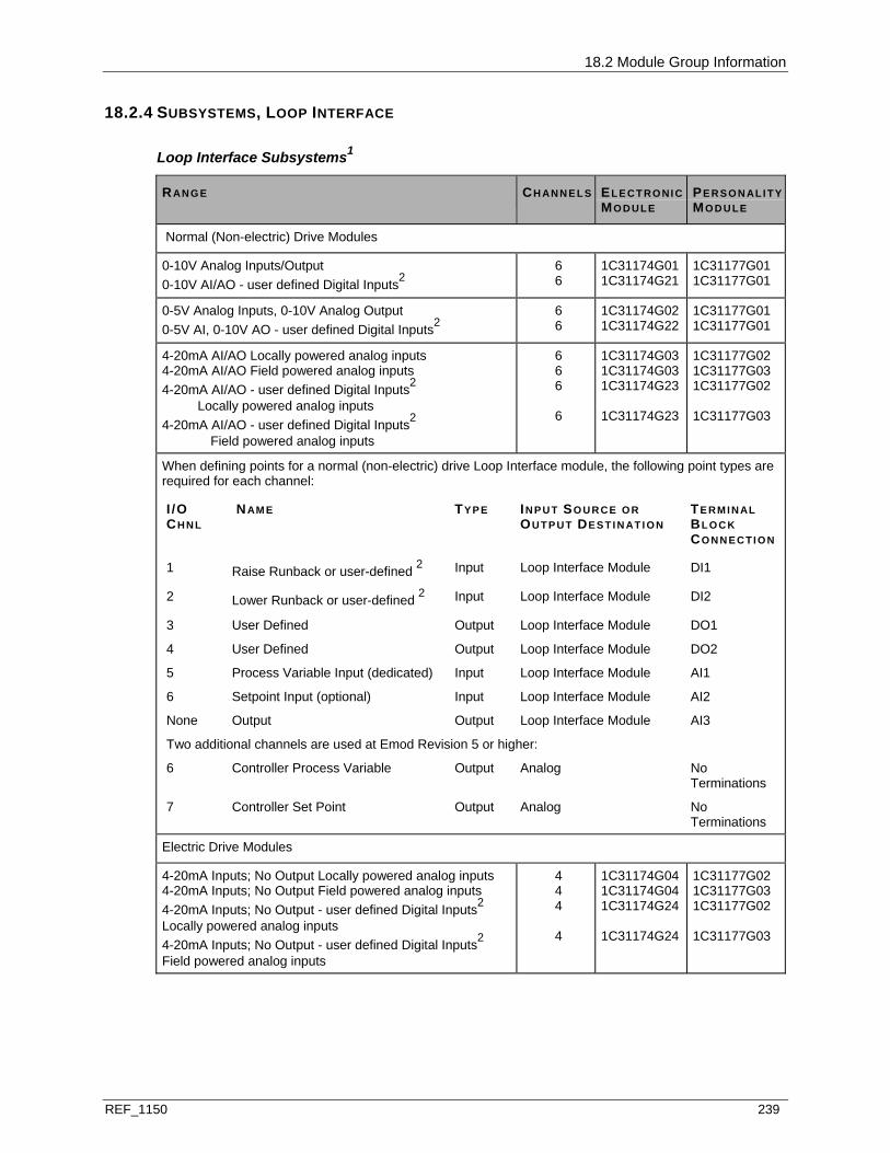
18.2 Module Group Information
REF_1150 239
18.2.4 SUBSYSTEMS, LOOP INTERFACE
Loop Interface Subsystems1
RANG E CH AN N E L S EL E CT RO NI C MO D U LE
PE R S O N AL I T Y MO D U LE
Normal (Non-electric) Drive Modules
0-10V Analog Inputs/Output 0-10V AI/AO - user defined Digital Inputs2
6 6
1C31174G01 1C31174G21
1C31177G01 1C31177G01
0-5V Analog Inputs, 0-10V Analog Output 0-5V AI, 0-10V AO - user defined Digital Inputs2
6 6
1C31174G02 1C31174G22
1C31177G01 1C31177G01
4-20mA AI/AO Locally powered analog inputs 4-20mA AI/AO Field powered analog inputs 4-20mA AI/AO - user defined Digital Inputs2 Locally powered analog inputs 4-20mA AI/AO - user defined Digital Inputs2 Field powered analog inputs
6 6 6
6
1C31174G03 1C31174G03 1C31174G23 1C31174G23
1C31177G02 1C31177G03 1C31177G02 1C31177G03
When defining points for a normal (non-electric) drive Loop Interface module, the following point types are required for each channel:
I /O CHNL
NAM E TYP E IN P U T SO U R CE O R OU T P U T DE S T I N AT I O N
TE RM I N AL BL O C K CO N N E C TI O N
1 Raise Runback or user-defined 2 Input Loop Interface Module DI1
2 Lower Runback or user-defined 2 Input Loop Interface Module DI2
3 User Defined Output Loop Interface Module DO1
4 User Defined Output Loop Interface Module DO2
5 Process Variable Input (dedicated) Input Loop Interface Module AI1
6 Setpoint Input (optional) Input Loop Interface Module AI2
None Output Output Loop Interface Module AI3
Two additional channels are used at Emod Revision 5 or higher:
6 Controller Process Variable Output Analog No Terminations
7 Controller Set Point Output Analog No Terminations
Electric Drive Modules
4-20mA Inputs; No Output Locally powered analog inputs 4-20mA Inputs; No Output Field powered analog inputs 4-20mA Inputs; No Output - user defined Digital Inputs2
Locally powered analog inputs 4-20mA Inputs; No Output - user defined Digital Inputs2
Field powered analog inputs
4 4 4
4
1C31174G04 1C31174G04 1C31174G24 1C31174G24
1C31177G02 1C31177G03 1C31177G02 1C31177G03

18.2 Module Group Information
240 REF_1150
RANG E CH AN N E L S EL E CT RO NI C MO D U LE
PE R S O N AL I T Y MO D U LE
When defining points for an electric drive Loop Interface module, the following point types are required for each channel:
I /O CHNL
NAM E TYP E IN P U T SO U R CE O R OU T P U T DE S T I N AT I O N
TE RM I N AL BL O C K CO N N E C TI O N
1 Raise Runback or user-defined 2 Input Loop Interface Module DI1
2 Lower Runback or user-defined 2 Input Loop Interface Module DI2
None Output Raise Pulse (dedicated) Output Loop Interface Module DO1
None Output Lower Pulse (dedicated) Output Loop Interface Module DO2
5 Process Variable Input (dedicated) Input Loop Interface Module AI1
6 Process Position (dedicated) Input Loop Interface Module AI2
None Output Output Output is compared to Process Position. Raise/Lower pulses (DO1, DO2) are generated as applicable.
No Terminations
Two additional channels are used at Emod Revision 5 or higher:
7 Controller Process Variable Output Analog No Terminations
8 Controller Set Point Output Analog No Terminations
1 This module will control ONE process loop. To use this module, the MASTATION algorithm must reside in the Ovation Controller. (See the Ovation Algorithm Reference Manual.) 2 Raise and Lower Runback inputs can be disabled and used as user-defined input points. Configuration instructions are included in Kit 1C31174G20. 3 This output may not appear on the termination list, but must be terminated for proper operation.
All Configurations are CE Mark Certified

18.3 Module Specific Information
REF_1150 241
18.3 MODULE SPECIFIC INFORMATION
18.3.1 MODES OF OPERATION
There are four modes of operation for the Loop Interface module:
Cascade Auto Manual (also supports Timed-out Manual sub-mode) Local (also supports Timed-out Local sub-mode)
Operation Modes
MO DE SOURCE FOR OU T P U T (DEM AND)
SOURCE FOR SE TPOI NT
Cascade Controller Controller
Auto Controller Controller or SLIM
Manual Controller or SLIM Controller or SLIM
Local 1 SLIM SLIM
1 When in Local mode, the Loop Interface module accepts mode change requests from the SLIM only.
Runbacks
For the Ovation Loop Interface module, the digital inputs perform the runback function. The digital inputs are used as priority raise or lower for the output. Priority action takes precedence over any output request from the Controller or SLIM. Runbacks may be used with either of the two module types (Normal (non-electric) or Electric Drive).
If desired, digital inputs as runbacks can be disabled and used as user-defined digital input points. In order to disable digital inputs as runback functions, the module must be configured per instructions on drawing 1C31174 (Groups 21-24).
18.3.2 MANUAL STATION CONTROL
The single-loop interface module may communicate to the Small Loop Interface Module (SLIM) via its RS-422 serial port. The serial port connector is located on the personality module. Alternatively, the serial port wiring may be connected directly at the terminal block.
A single SLIM will communicate with one Loop Interface module. Multiple Loop Interface modules per single SLIM are not supported. SLIMs are not required for the loop interface module operation. (The loop interface module may be used without a SLIM.)
18.3 Module Specific Information
242 REF_1150
18.3.3 NORMAL AND INVERSE ANALOG OUTPUT
A wire jumper between terminals IAO and logic GND can be used to set the analog output to Inverse Operation.
Normal (default - no wire installed) operation of the analog output means that when the output value is 0% (as seen at the SLIM or Controller), the analog output is a minimum (0V for groups 1 and 2, or 4mA for groups 3 and 4 modules). When the output value is 100%, the actual analog output is at its maximum value (+10V for group 1, +5V for group 2, and 20mA for groups 3 and 4 modules).
Inverse (wire jumper installed) operation of the analog output means that when the output value is 0% (as seen at the SLIM or Controller), the analog output is a maximum (+10V for group 1, +5V for group 2, and 20mA for groups 3 and 4 modules). When the output value is 100%, the analog output is its minimum value (0V for groups 1 and 2, or 4mA for groups 3 and 4 modules).
18.3.4 EXTERNAL POWER SUPPLIES
If the Loop Interface subsystem uses the 1C31177G02 Personality module (configured for two 4 to 20 mA current analog inputs that are locally powered), the required voltage supply may be obtained from the internal Ovation auxiliary power supply (available through the terminal block), or it may be obtained from an external power supply.
If an external power supply is used, Using an External Power Supply (see page 539) contains steps to be undertaken before connecting the external power supply to the Loop Interface module base unit terminal block. The Loop Interface module auxiliary supply voltage level (24 VDC or 48 VDC) depends on the external transmitter devices being interfaced to the Loop Interface module’s analog inputs.
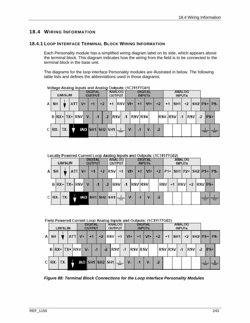
18.4 Wiring Information
REF_1150 243
18.4 WIRING INFORMATION
18.4.1 LOOP INTERFACE TERMINAL BLOCK WIRING INFORMATION
Each Personality module has a simplified wiring diagram label on its side, which appears above the terminal block. This diagram indicates how the wiring from the field is to be connected to the terminal block in the base unit.
The diagrams for the loop interface Personality modules are illustrated in below. The following table lists and defines the abbreviations used in those diagrams.
Figure 88: Terminal Block Connections for the Loop Interface Personality Modules
18.4 Wiring Information
244 REF_1150
Loop Interface Terminal Block Wiring Information
SE C TI ON AB B R E V I AT I ON
DE FI NI T I O N
SH 2 Shield terminal connection
Logic ground
ATT Attention
RX ± Receive data
LIM/SLIM (see page 407) 1
TX ± Transmit data
V ± Voltage source terminal connection
± 1, ± 2 Positive or negative terminal connection
DIGITAL OUTPUT
SH1, SH2 2 Shield terminal connection
± 1 Positive or negative terminal connection
SH1 2 Shield terminal connection
Earth ground terminals
ANALOG OUTPUT 3
IAO When connected to logic ground, results in an inverse analog output (see page 242) operation.
± 1, ± 2 Positive or negative terminal connection
V- Fused voltage source terminal ground connection
DIGITAL INPUTS 4
Vf+ Fused voltage source terminal connection
± 1, ± 2 Positive or negative terminal connection
SH1, SH2 2 Shield terminal connection
ANALOG INPUTS 5
P1+, P2+ Positive terminal connection for current loop power
PS ± PS ± Auxiliary power supply terminals
Earth GND Earth ground terminals
RSV RSV Reserved. No connections allowed on these terminals.

18.4 Wiring Information
REF_1150 245
SE C TI ON AB B R E V I AT I ON
DE FI NI T I O N
1 No connections to terminals are required when using a SLIM cable (5A26166) connected to a Loop Interface Personality module in non-CE Mark certified systems. In CE Mark systems, SLIM cable 5A26429 MUST be used and grounded at the entry point of the cabinet using the recommended hardware (refer to the appropriate “Cable Guidelines” information for your system). 2 Non-CE Mark certified systems only. 3 For Group 3 current Loop Interface modules, analog output MUST be connected for proper operation, or an analog output error will be reported. 4 If digital inputs as runbacks are not desired (but are enabled), a shorting wire MUST be placed across inputs (+1 to -1 and +2 to -2) to eliminate false turn on from noise. 5 For Group 3 and 4 current Loop Interface modules, analog inputs MUST be connected for proper operation, or an analog input error will be reported.
Note: Do not use unmarked terminal block locations or locations marked RSV. Shield terminals (SH) are not connected in CE Mark systems. The analog output is not present on Electric Drive modules.

18.4 Wiring Information
246 REF_1150
18.4.2 LOOP INTERFACE FIELD CONNECTION WIRING DIAGRAMS
Non-CE Mark Certified Systems
Figure 89: Voltage Analog Input Field Connections (Non-CE Mark)

18.4 Wiring Information
REF_1150 247
Figure 90: Jumper Settings for Voltage Analog Input Personality Module
Pmod
AIN+2
+-
AIN-2
Terminal BlockAI section
P1+
+1SH1
P2+
+2SH2
Emod
Fuse
+- AIN+1
AIN-1
Fuse
PS+
PS-
+-AuxPS

18.4 Wiring Information
248 REF_1150
Figure 91: Locally Powered Current Analog Input Field Connections (Non-CE Mark)
AIN+1
Pmod (PLIF)
-+
AIN+2
AIN-1
AIN-2
Terminal BlockAI section
+1
-1SH1
+2
-2SH2
Emod (FLI)
+-Fuse
Fuse-+
+-
Field PowerSupply
Field PowerSupply
Rsv
Rsv
Figure 92: Field Powered Current Analog Input Field Connections (Non-CE Mark)
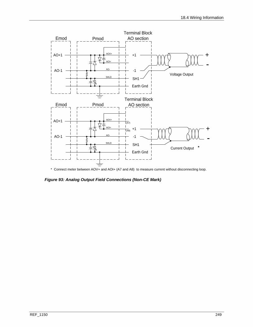
18.4 Wiring Information
REF_1150 249
AO+1
Pmod
+-
AO-1
Terminal BlockAO section
+1
-1
SH1
Emod
Voltage Output
AOV+
Earth Gnd
AOI+
AO-
SHLD
AO+1
Pmod
+-AO-1
Terminal BlockAO section
(A7)
+1
-1
SH1
Emod
Current Output
AOV+
(A8)
Earth Gnd
AOI+
AO-
SHLD
*
* Connect meter between AOV+ and AOI+ (A7 and A8) to measure current without disconnecting loop.
Figure 93: Analog Output Field Connections (Non-CE Mark)
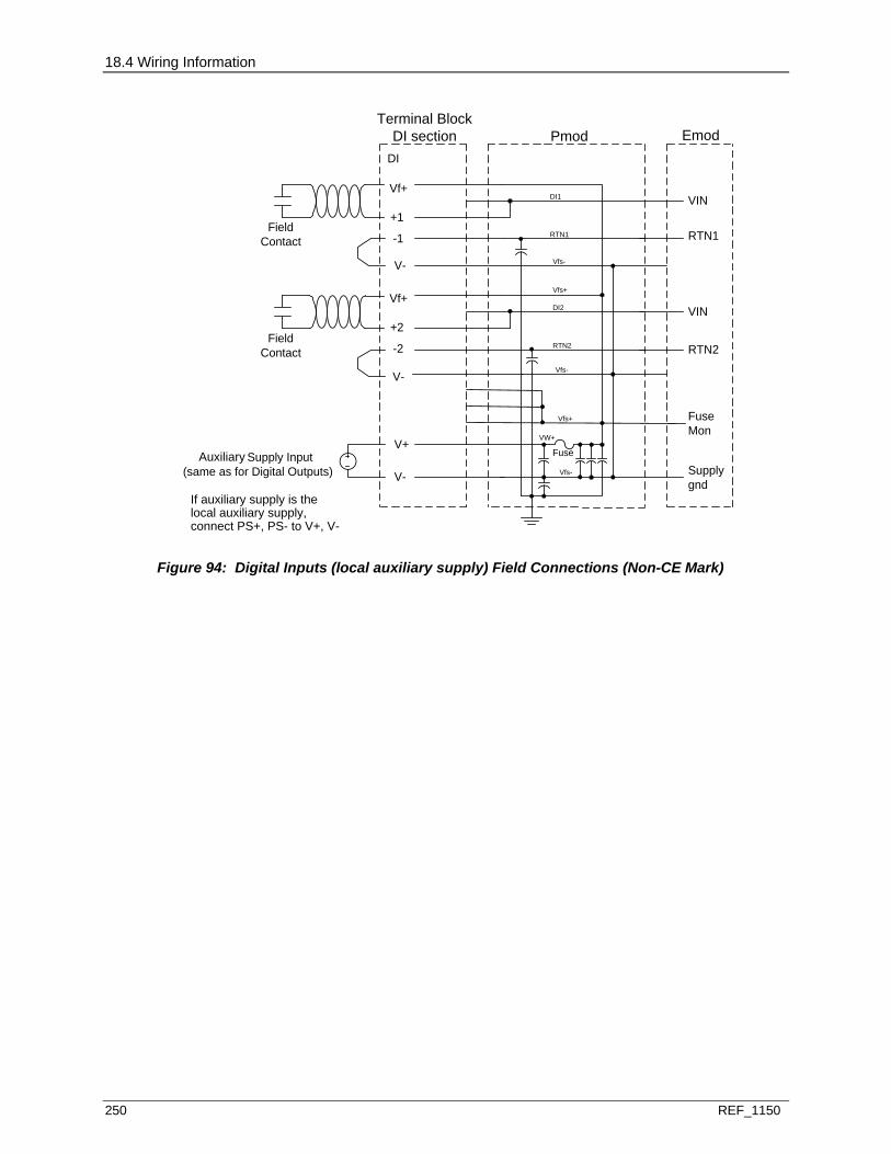
18.4 Wiring Information
250 REF_1150
VIN
Pmod
RTN1
Terminal BlockDI section
+1
-1
Emod
FieldContact
DI
Vf+
V-
+2
-2Field
Contact
Vf+
V-
V-
V+Wetting Supply Input
(same as for Digital Outputs)Fuse
RTN2
VINDI2
DI1
RTN2
RTN1
Vfs+
VW+
Vfs-
Vfs-
Vfs+
Vfs-
FuseMon
Supplygnd
If Aux. supply = wetttingsupply: connect PS+, PS- to
V+, V-
If auxiliary supply is thelocal auxiliary supply,connect PS+, PS- to V+, V-
Auxiliary
Figure 94: Digital Inputs (local auxiliary supply) Field Connections (Non-CE Mark)
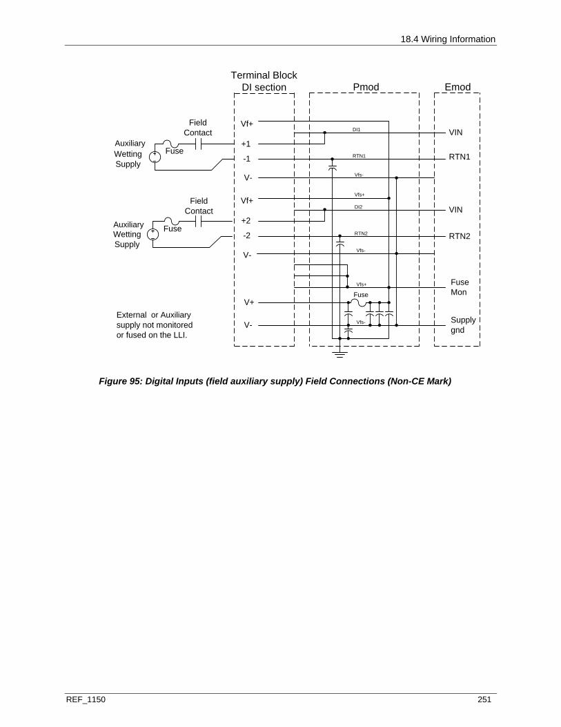
18.4 Wiring Information
REF_1150 251
VIN
Pmod
RTN1
Terminal BlockDI section
+1
-1
Emod
FieldContact
Vf+
V-
+2
-2
Vf+
V-
V-
V+Fuse
RTN2
VINDI2
DI1
RTN2
RTN1
Vfs+
Vfs-
Vfs-
Vfs+
Vfs-
FuseMon
Supplygnd
FieldContact
ExternalWettingSupply
ExternalWettingSupply
Fuse
Fuse
External Wettingsupply not monitoredor fused on the LLI.
Auxiliary
Auxiliary
or Auxiliary
Figure 95: Digital Inputs (field auxiliary supply) Field Connections (Non-CE Mark)

18.4 Wiring Information
252 REF_1150
DO1-
Pmod (PLIV, PLIL, PLIF)Terminal Block
DO section
SH1
Emod (FLI)
+1
-2
+2
SH2
V-
V+ Wetting SupplyInput
Fuse
DO2-
DO1-
DO2-
DO1SHLD
VW+
DO2SHLD
Vfs+
Vfs-
FuseMon
Rtn
Vfs+
-1
Vfs+
D
G
S
D
G
S
Vf
Vf
Rsv
If Aux supply = wetting supply:connect PS+, PS- to V+,V-
LOAD
LOAD
Auxiliary
If auxiliary supply is thelocal auxiliary supply,connect PS+, PS- to V+, V-
Figure 96: Digital Outputs (local aux supply) Field Connections (Non-CE Mark)
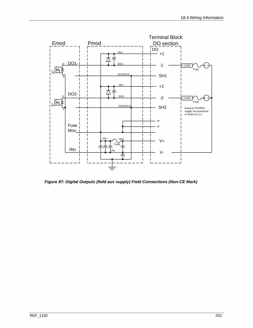
18.4 Wiring Information
REF_1150 253
DO1-
Pmod (PLIV, PLIL, PLIF)Terminal Block
DO section
SH1
Emod (FLI)DO
+1
-2
+2
SH2
V-
V+Fuse
DO2-
DO1-
DO2-
DO1SHLD
VW+
DO2SHLD
Vfs+
Vfs-
FuseMon
Rtn
Vfs+
-1
Vfs+
D
G
S
D
G
S
Vf
Vf
Rsv
External Wettingsupply not monitoredor fused on LLI.
Fuse
Fuse
LOAD
LOAD
Auxiliaryl Auxiliary
Figure 97: Digital Outputs (field aux supply) Field Connections (Non-CE Mark)
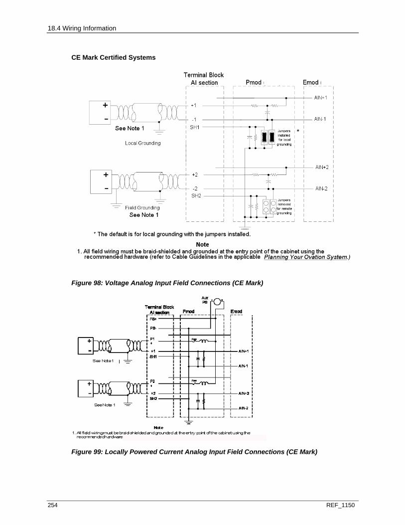
18.4 Wiring Information
254 REF_1150
CE Mark Certified Systems
Figure 98: Voltage Analog Input Field Connections (CE Mark)
Figure 99: Locally Powered Current Analog Input Field Connections (CE Mark)
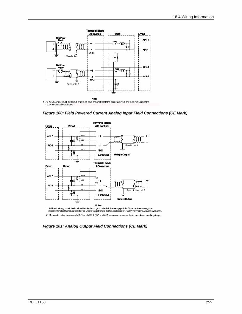
18.4 Wiring Information
REF_1150 255
Figure 100: Field Powered Current Analog Input Field Connections (CE Mark)
Figure 101: Analog Output Field Connections (CE Mark)
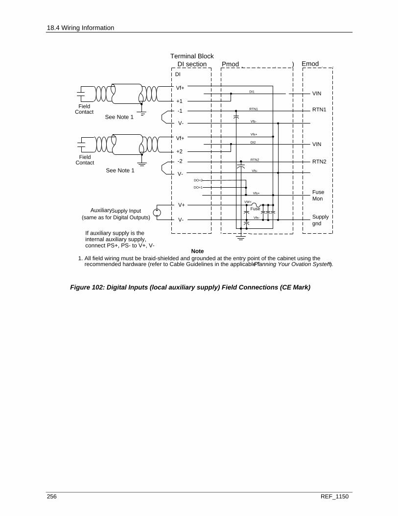
18.4 Wiring Information
256 REF_1150
VIN
Pmod (PLIV, PLIL, PLIF)
RTN1
Terminal BlockDI section
+1
-1
Emod (FLI)
FieldContact
DI
Vf+
V-
+2
-2
Vf+
V-
V-
V+Wetting Supply Input
(same as for Digital Outputs)Fuse
Rsv
Rsv
RTN2
VINDI2
DI1
RTN2
RTN1
Vfs+
VW+
Vfs-
Vfs-
Vfs+
Vfs-
FuseMon
Supplygnd
DO+2
DO+1
Rsv
If Aux. supply = wetttingsupply: connect PS+, PS- to
V+, V-
FieldContact
SEE NOTE 1
Auxiliary
If auxiliary supply is theinternal auxiliary supply,connect PS+, PS- to V+, V-
See Note 1
See Note 1
1. All field wiring must be braid-shielded and grounded at the entry point of the cabinet using theNote
recommended hardware (refer to Cable Guidelines in the applicable "Planning Your Ovation System").
Figure 102: Digital Inputs (local auxiliary supply) Field Connections (CE Mark)

18.4 Wiring Information
REF_1150 257
VIN
Pmod (PLIV, PLIL, PLIF)
RTN1
Terminal BlockDI section
+1
-1
Emod (FLI)
FieldContact
Vf+
V-
+2
-2
Vf+
V-
V-
V+Fuse
Rsv
Rsv
RTN2
VINDI2
DI1
RTN2
RTN1
Vfs+
VW+
Vfs-
Vfs-
Vfs+
Vfs-
FuseMon
Supplygnd
ExternalWettingSupply
DO+2
DO+1
Rsv
Fuse
ExternalWetting supplynot monitored orfused on LLI.
FieldContact
ExternalWettingSupply
Fuse
SEE NOTE 1
auxiliary
Auxiliary
Auxiliary
See Note 1
See Note 1
1. All field wiring must be braid-shielded and grounded at the entry point of the cabinet using theNote
recommended hardware (refer to Cable Guidelines in the applicable "Planning Your Ovation System").
Figure 103: Digital Inputs (field auxiliary supply) Field Connections (CE Mark)
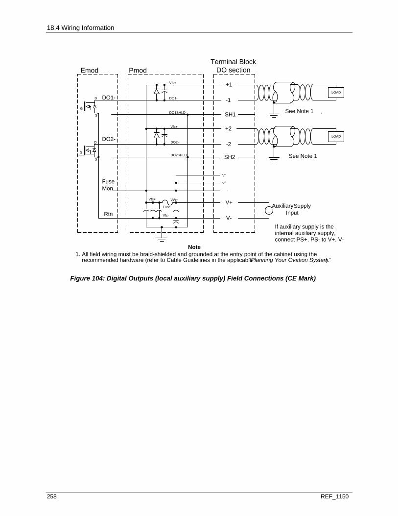
18.4 Wiring Information
258 REF_1150
DO1-
Pmod (PLIV, PLIL, PLIF)Terminal Block
DO section
SH1
Emod (FLI)
+1
-2
+2
SH2
V-
V+ Wetting SupplyInput
Fuse
DO2-
DO1-
DO2-
DO1SHLD
VW+
DO2SHLD
Vfs+
Vfs-
FuseMon
Rtn
Vfs+
-1
Vfs+
D
G
S
D
G
S
Vf
Vf
Rsv
If Aux supply = wetting supply:connect PS+, PS- to V+,V-
LOAD
LOAD
SEE NOTE 1
Auxiliary
If auxiliary supply is theinternal auxiliary supply,connect PS+, PS- to V+, V-
See Note 1
See Note 1
1. All field wiring must be braid-shielded and grounded at the entry point of the cabinet using theNote
recommended hardware (refer to Cable Guidelines in the applicable "Planning Your Ovation System").
Figure 104: Digital Outputs (local auxiliary supply) Field Connections (CE Mark)

18.4 Wiring Information
REF_1150 259
DO1-
Pmod (PLIV, PLIL, PLIF)Terminal Block
DO section
SH1
Emod (FLI)DO
+1
-2
+2
SH2
V-
V+Fuse
DO2-
DO1-
DO2-
DO1SHLD
VW+
DO2SHLD
Vfs+
Vfs-
FuseMon
Rtn
Vfs+
-1
Vfs+
D
G
S
D
G
S
Vf
Vf
Rsv
External Wettingsupply not monitoredor fused on LLI.
Fuse
Fuse
LOAD
LOAD
SEE NOTE 1
auxiliary
See Note 1
1. All field wiring must be braid-shielded and grounded at the entry point of the cabinet using theNote
recommended hardware (refer to Cable Guidelines in the applicable "Planning Your Ovation System").
Figure 105: Digital Outputs (field auxiliary supply) Field Connections (CE Mark)
18.4.3 SLIM SERIAL PORT CONNECTOR
The Personality module SLIM connector is used to connect the Loop Interface module to a SLIM module.
SLIM Connector (J1 RS-485) Pin Assignments
PI N NUM BE R SI G N AL NAM E (FUNCTI O N) S I G N AL DI RECT I O N
1 SP-COMMON NA
2 RX - (Receive Data) Input
3 Shd (Cable Shield) NA
4 RX+ (Receive Data) Input
5 SLIM-ATT/(SLIM Cable Connector Attached) 1 Input
6 TX+ (Transmit Data) Output
7 No connection NA
8 TX- (Transmit Data) Output
9 SP-COMMON NA
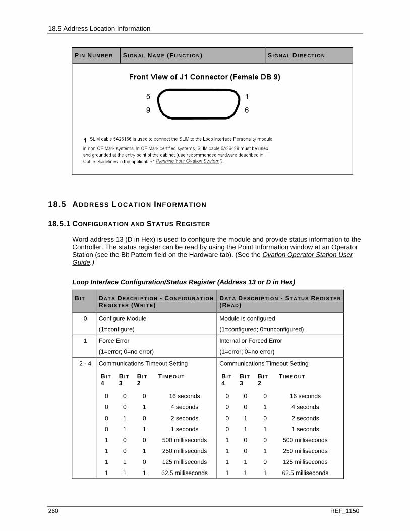
18.5 Address Location Information
260 REF_1150
PI N NUM BE R SI G N AL NAM E (FUNCTI O N) S I G N AL DI RECT I O N
18.5 ADDRESS LOCATION INFORMATION
18.5.1 CONFIGURATION AND STATUS REGISTER
Word address 13 (D in Hex) is used to configure the module and provide status information to the Controller. The status register can be read by using the Point Information window at an Operator Station (see the Bit Pattern field on the Hardware tab). (See the Ovation Operator Station User Guide.)
Loop Interface Configuration/Status Register (Address 13 or D in Hex)
BI T DAT A DE S C R I P T I O N - CO NF I G U R AT I O N RE GI S T E R (WRI T E)
DAT A DE S C R I P T I O N - ST ATUS REGI S TER (RE AD)
0 Configure Module
(1=configure)
Module is configured
(1=configured; 0=unconfigured)
1 Force Error
(1=error; 0=no error)
Internal or Forced Error
(1=error; 0=no error)
2 - 4 Communications Timeout Setting
BI T 4
BI T 3
BI T 2
T I M EO U T
0 0 0 16 seconds
0 0 1 4 seconds
0 1 0 2 seconds
0 1 1 1 seconds
1 0 0 500 milliseconds
1 0 1 250 milliseconds
1 1 0 125 milliseconds
1 1 1 62.5 milliseconds
Communications Timeout Setting
BI T 4
BI T 3
BI T 2
T I M EO U T
0 0 0 16 seconds
0 0 1 4 seconds
0 1 0 2 seconds
0 1 1 1 seconds
1 0 0 500 milliseconds
1 0 1 250 milliseconds
1 1 0 125 milliseconds
1 1 1 62.5 milliseconds
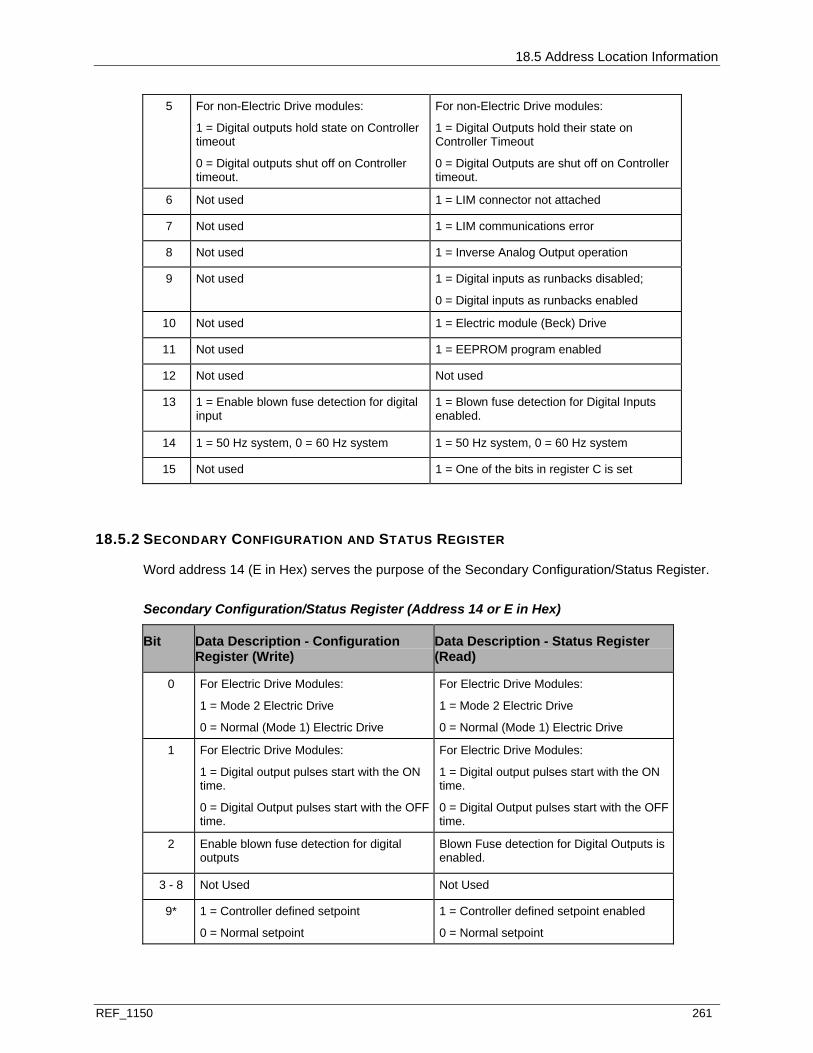
18.5 Address Location Information
REF_1150 261
5 For non-Electric Drive modules:
1 = Digital outputs hold state on Controller timeout
0 = Digital outputs shut off on Controller timeout.
For non-Electric Drive modules:
1 = Digital Outputs hold their state on Controller Timeout
0 = Digital Outputs are shut off on Controller timeout.
6 Not used 1 = LIM connector not attached
7 Not used 1 = LIM communications error
8 Not used 1 = Inverse Analog Output operation
9 Not used 1 = Digital inputs as runbacks disabled;
0 = Digital inputs as runbacks enabled
10 Not used 1 = Electric module (Beck) Drive
11 Not used 1 = EEPROM program enabled
12 Not used Not used
13 1 = Enable blown fuse detection for digital input
1 = Blown fuse detection for Digital Inputs enabled.
14 1 = 50 Hz system, 0 = 60 Hz system 1 = 50 Hz system, 0 = 60 Hz system
15 Not used 1 = One of the bits in register C is set
18.5.2 SECONDARY CONFIGURATION AND STATUS REGISTER
Word address 14 (E in Hex) serves the purpose of the Secondary Configuration/Status Register.
Secondary Configuration/Status Register (Address 14 or E in Hex)
Bit Data Description - Configuration Register (Write)
Data Description - Status Register (Read)
0 For Electric Drive Modules:
1 = Mode 2 Electric Drive
0 = Normal (Mode 1) Electric Drive
For Electric Drive Modules:
1 = Mode 2 Electric Drive
0 = Normal (Mode 1) Electric Drive
1 For Electric Drive Modules:
1 = Digital output pulses start with the ON time.
0 = Digital Output pulses start with the OFF time.
For Electric Drive Modules:
1 = Digital output pulses start with the ON time.
0 = Digital Output pulses start with the OFF time.
2 Enable blown fuse detection for digital outputs
Blown Fuse detection for Digital Outputs is enabled.
3 - 8 Not Used Not Used
9* 1 = Controller defined setpoint
0 = Normal setpoint
1 = Controller defined setpoint enabled
0 = Normal setpoint
18.6 Diagnostic LEDs
262 REF_1150
10* 1 = Controller defined process variable
0 = Normal PV operation
1 = Controller defined process variable enabled
0 = Normal process variable operation
11 - 15* Not Used Not Used
* Software supported only for Emods Rev 5 and higher.
18.5.3 POINT QUALITY REGISTER
Word address 12 (C in Hex) serves the purpose of reporting the point quality.
Point Quality Register (Address 12 or C in Hex)
Bit Write Definition Read Definition
0 Not used 1 = Analog Input 1 auto calibration reasonability check failed
1 Not used 1 = Analog Input 1 over-range, blown fuse or open loop
2 Not used 1 = Analog Input 1 auto calibration reasonability check failed
3 Not used 1 = Analog Input 1 over-range, blown fuse or open loop
4 Not used 1 = Analog Input auxiliary supply blown fuse monitored and detected
5 Not used 1 = Analog Output over current
6 Not used 1 = Analog Output undercurrent
7 Not used 1 = Runback error (both raise and lower runbacks are active)
8 - 15 Not used Internal (Initialization) Error Codes
18.6 DIAGNOSTIC LEDS
The following table lists the module’s LEDs and describes what they mean when lit.
Loop Interface Diagnostic LEDs
LED DE S C RI P TI O N
P (Green) Power OK LED. Lit when the +5V power is OK.
C (Green) Communications OK LED. Lit when the Controller is communicating with the module.

18.6 Diagnostic LEDs
REF_1150 263
LED DE S C RI P TI O N
I (Red) Internal Error LED. Lit whenever there is any type of error with the module. Possible causes are: I/O bus communications watchdog timeout. Forced error issued by the Controller. Initialization error (SRAM error, invalid group, and so forth). Microcontroller watchdog timer timeout or module reset.
1 AO (Red) Analog Output Error. Lit whenever there is an over current or undercurrent condition on the analog output section (Group 3 and 4 only).
2 AI1,
3 AI2 (Red)
Analog Input Error. Lit whenever there is an input error. Possible causes are: Input voltage over-range for 10 seconds. Broken current loop input/blown fuse for module configured as current input. Offset calibration voltage out of range for five consecutive calibrations (40 seconds).
4 Fuse (Red) Blown Fuse Error. Lit if the auxiliary supply voltage for either the digital inputs or digital outputs is not present and blown fuse detection is enabled for either the digital outputs or the digital inputs.
5 SLIM (Red) SLIM Communication Error. Lit if there is a SLIM serial port communications error.
6 DO1 (Green) Digital Output Status. Lit when digital output 1 is active.
7 DO2 (Green) Digital Output Status. Lit when digital output 2 is active.
8 DI1 (Green) Digital Input Status. Lit when digital input 1 is active.
9 DI2 (Green) Digital Input Status. Lit when digital input 2 is active.
18.7 Specifications
264 REF_1150
18.7 SPECIFICATIONS
Electronics Module (1C31174)
Personality Module (1C31177)
The following tables provide specifications for the Loop Interface module:
General Specifications Analog input Analog output Digital input Digital output).
Loop Interface General Specifications
DE S C RI P TI O N VALUE
Module power Main: 2.7 W typical; 3.5 W maximum
Aux (when used):
Digital Inputs:
0.13W (24V) typical
0.27 W (48V) typical Digital Outputs:
(power-dependent on loads for 2 outputs @ 100mA each)
4.8 W (24V) typical
9.6 W (48V) typical Analog Inputs:
(2 inputs @ 20mA each)
0.96 W (24V) typical
Operating temperature range 0 to 60°C (32°F to 140°F)
Storage temperature range -40°C to 85°C (-40°F to 185°F)
Humidity (non-condensing) 0 to 95%
Loop Interface Analog Input Module Specifications
DE S C RI P TI O N VAL UE
Number of analog input points 2
Input range 0 to +10 V (G01)
0 to +5 V (G02)
4 to 20 mA (G03 - G04)
AI1 and AI2 current inputs must be terminated (even if not used) to prevent point fault generation.

18.7 Specifications
REF_1150 265
DE S C RI P TI O N VAL UE
Resolution 13 bits (including polarity)
Guaranteed accuracy (@25°C) 1 ±0.10% of upper range value ±10μV ±1/2LSB @99.7% confidence
Temperature coefficient ±0.24% of the upper range value ±24μV over 0 to 60°C.
Input impedance:
0 to 10V groups
0 to 5V groups, and 4 to 20mA groups
2 MΩ
1 MΩ
Sampling rate 10 samples per second under normal conditions.
8 samples per second during auto calibration.
Offset and gain temperature drift compensation
Automatic
Diagnostics Internal module operating faults.
Out of range detection.
Open loop/blown fuse detection for current loops.
Dielectric isolation:
Channel to channel
Channel to logic
1000 V AC/DC
1000 V AC/DC
Normal mode rejection 60 dB at 50 Hz ± 1/2% or 60 Hz ± 1/2%
30 dB (typical) at 50 Hz ± 5% or 60 Hz ± 5%
Common mode rejection 120 dB at DC; power line frequency and its harmonics ± 1/2% without line frequency tracking.
100 dB (typical) for nominal line frequency ± 5% and harmonics without line frequency tracking.
1 See additional information for CE Mark certified systems.
Loop Interface Analog Output Module Specifications
DE S C RI P TI O N VALUE
Number of points 1 - Analog output is not present for Group 4 (electric drive) modules.
AO current outputs in G03 - G04 must be terminated (even if not used) to prevent point fault generation.
Maximum update time 2 mSec
Output range 0 - 10 V@ minimum 1 kΩ load impedance (10mA maximum load) (G01 - G02)
4 - 20 mA @ maximum 750 Ω load impedance (0 Ω minimum) (G03)
Resolution 12 bits
18.7 Specifications
266 REF_1150
DE S C RI P TI O N VALUE
Guaranteed accuracy (@25°C ± 1°C) 1
±0.10% of span
Temperature coefficient 0 to 10 V groups: 30 ppm/°C
4 to 20mA groups: 45 ppm/°C
User loop voltage Power for current loop output is supplied by module.
Diagnostics Internal module operating faults Overcurrent Undercurrent
Dielectric isolation:
Channel ground to channel ground
Channel ground to logic ground
Maximum ± 1000 V AC/DC
Maximum ± 1000 V AC/DC
Output loading
0 - 10 V@ minimum 1 kΩ load impedance (10mA maximum load)
4 - 20 mA @ maximum 750 Ω load impedance (0 Ω minimum)1 See additional information for CE Mark certified systems (see page 537).
Loop Interface Digital Input Module Specifications
DE S C RI P TI O N VALUE
Number of points Two digital inputs dedicated as runback inputs. If runbacks are not desired, shorting wires should be placed across the inputs (+1 to -1 and +2 to -2) to eliminate possible false turn on from noise.
Input range 24V or 48V typ 18 -60 VDC
Propagation delay of contact change of state
1.9 mSec minimum; 35.0 mSec maximum
Cable length (quality is 50pF/ft or better)
1000 feet maximum
Diagnostics Internal module operating faults Auxiliary power supply blown fuse detection (enabled/disabled)
Runback error (both raise and lower active)
Dielectric isolation:
Channel ground to channel ground
Channel ground to logic ground
Maximum 1000V AC/DC
Maximum 1000V AC/DC
External (auxiliary) power supply If desired, the digital input auxiliary supply voltage may be the same voltage as that used for the digital outputs. This voltage is provided as an output between terminals Vf+ and V-. This fused voltage (Vf+) is monitored as an additional digital input. Input characteristics are identical to the other two digital inputs.
18.7 Specifications
REF_1150 267
Loop Interface Digital Output Module Specifications
DE S C RI P TI O N VALUE
Number of points 2
Output voltage
Off voltage (maximum)
On voltage (maximum)
5 VDC minimum, 60 VDC maximum (auxiliary power supply)
1.0 VDC @ 500mA
Output current
Off current (maximum)
On current for individual output (maximum)
On current for two outputs combined (maximum)
25mA @ TA=25×C, VDS=60 VDC
250mA @ TA=60×C, VDS=60 VDC
500 mA
880 mA limited by fuse rating
External (auxiliary) supply voltage Voltage = 5 VDC minimum, 60 VDC maximum
The return line and auxiliary power supply voltage is common to both points but is galvanically isolated from logic ground. This auxiliary supply voltage originates from the terminal block (on inputs V+ and V-) and is fused on the personality module.
The fused voltage is distributed back out to the terminal blocks as +1, +2 for the digital outputs and Vf+ for the digital inputs. Each digital output is diode clamped to this fused auxiliary supply voltage to prevent damage from inductive load surges.
The fused auxiliary supply voltage is monitored as an additional digital input. Input characteristics are identical to the digital inputs.
Diagnostics Internal module operation faults
Auxiliary supply blown fuse detection (enabled/disabled)
Maximum propagation time 14.5 mSec for Rload=500W
This time is comprised of the microprocessor firmware digital output update rate, which is once per loop, or approximately every 12 ms, plus the delay time for the output, which is 2.5 ms max at Rload = 500 W.
Dielectric isolation:
Channel ground to logic ground
Maximum ±1000V AC/DC

REF_1150 269
IN THIS SECTION
Description ......................................................................................................................269 Module Group Information ..............................................................................................269 Wiring Information ...........................................................................................................271 Address Location Information .........................................................................................281 Diagnostic LEDs..............................................................................................................285 Specifications ..................................................................................................................286
19.1 DESCRIPTION
The Pulse Accumulator Module accumulates pulses for two input channels and provides the information to the Controller. There are three possible configurations:
Counting pulses over a defined period of time allows the module to measure the speed of the input pulses (frequency).
Counting pulses until instructed to stop counting either by the Ovation Controller or by an external field control input.
Measuring the time duration of a pulse.
The Pulse Accumulator Module is applicable for CE Mark Certified Systems.
Note: I/O Module General Information (see page 15) contains environmental, installation, wiring, and fuse information for I/O modules.
19.2 MODULE GROUP INFORMATION
19.2.1 ELECTRONICS MODULES (EMODS)
There are two groups of Electronics modules for the Pulse Accumulator Module:
1C31147G01 provides for pulse accumulation at one of three possible pulse input levels: 24/48 V (CT+ and CT- inputs). May be referenced to either negative or positive field
signal power supply common. Applicable for CE Mark.
12 V medium speed (MC+ and HM- inputs). Not applicable for CE Mark.
5 V medium speed (HC+ and HM-). Not applicable for CE Mark. 1C31147G02 provides for pulse accumulation at 5 V high speed (HC+ and
HM-). Not applicable for CE Mark certified systems.
S E C T I O N 1 9
PULSE ACCUMULATOR MODULE
19.2 Module Group Information
270 REF_1150
19.2.2 PERSONALITY MODULES (PMODS)
There are three groups of Personality modules for the Pulse Accumulator Module:
1C31150G01 accepts 24/48 V count and control inputs from dry contacts or from open-collector transistor drivers. The input signals are low-true and are referenced to the branch internal auxiliary power supply return (common negative).
1C31150G02 accepts 24/48 V count and control inputs from dry contacts. The input signals are high-true and are referenced to the branch internal auxiliary power supply positive rail (common positive).
1C31150G03 provides dedicated 24/48 V count and control field input power for just this Pulse Accumulator Electronics module. The field input power is obtained from an external DC power supply that is connected to two base unit terminal block terminals (DSA and DSB).
Pulse Accumulator Subsystem1
COUNT IN P U T LEV E L
CO N T R OL (ENABLE AND SNAPSHOT) INP UT LE VEL
CH AN N E L S EL E CT RO NI C MO D U LE
PE R S O N AL I T Y MO D U LE
24/48 V Medium Speed
24/48 V Medium Speed
Local field pwr. common neg.
Local field pwr. common pos.
Ext. field pwr. common pos. or neg.
2
2
2
1C31147G01
1C31147G01
1C31147G01
1C31150G01
1C31150G02
1C31150G03
5/12 V Medium Speed
24/48 V Medium Speed
Local field pwr. common neg.
Local field pwr. common pos.
Ext. field pwr. common pos. or neg
2
2
2
1C31147G01
1C31147G01
1C31147G01
1C31150G01
1C31150G02
1C31150G03
5 V High Speed
24/48 V Medium Speed
Local field pwr. common neg.
Local field pwr. common pos.
Ext. field pwr. common pos. or neg
2
2
2
1C31147G02
1C31147G02
1C31147G02
1C31150G01
1C31150G02
1C31150G03 1 To use this module, the algorithm RPACNT or RPAWIDTH must reside in the Ovation Controller. Refer to the appropriate Algorithm Reference Manual for your system for detailed information about the RPACNT and RPAWIDTH algorithms.
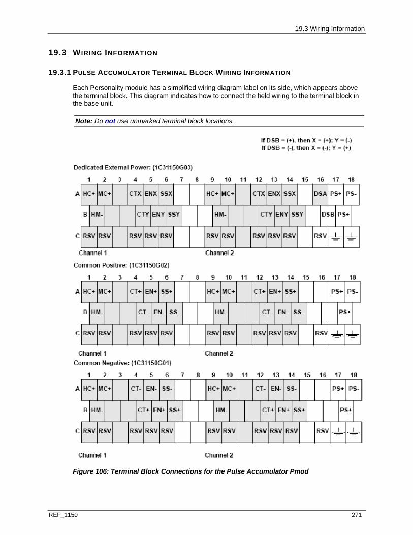
19.3 Wiring Information
REF_1150 271
19.3 WIRING INFORMATION
19.3.1 PULSE ACCUMULATOR TERMINAL BLOCK WIRING INFORMATION
Each Personality module has a simplified wiring diagram label on its side, which appears above the terminal block. This diagram indicates how to connect the field wiring to the terminal block in the base unit.
Note: Do not use unmarked terminal block locations.
Figure 106: Terminal Block Connections for the Pulse Accumulator Pmod
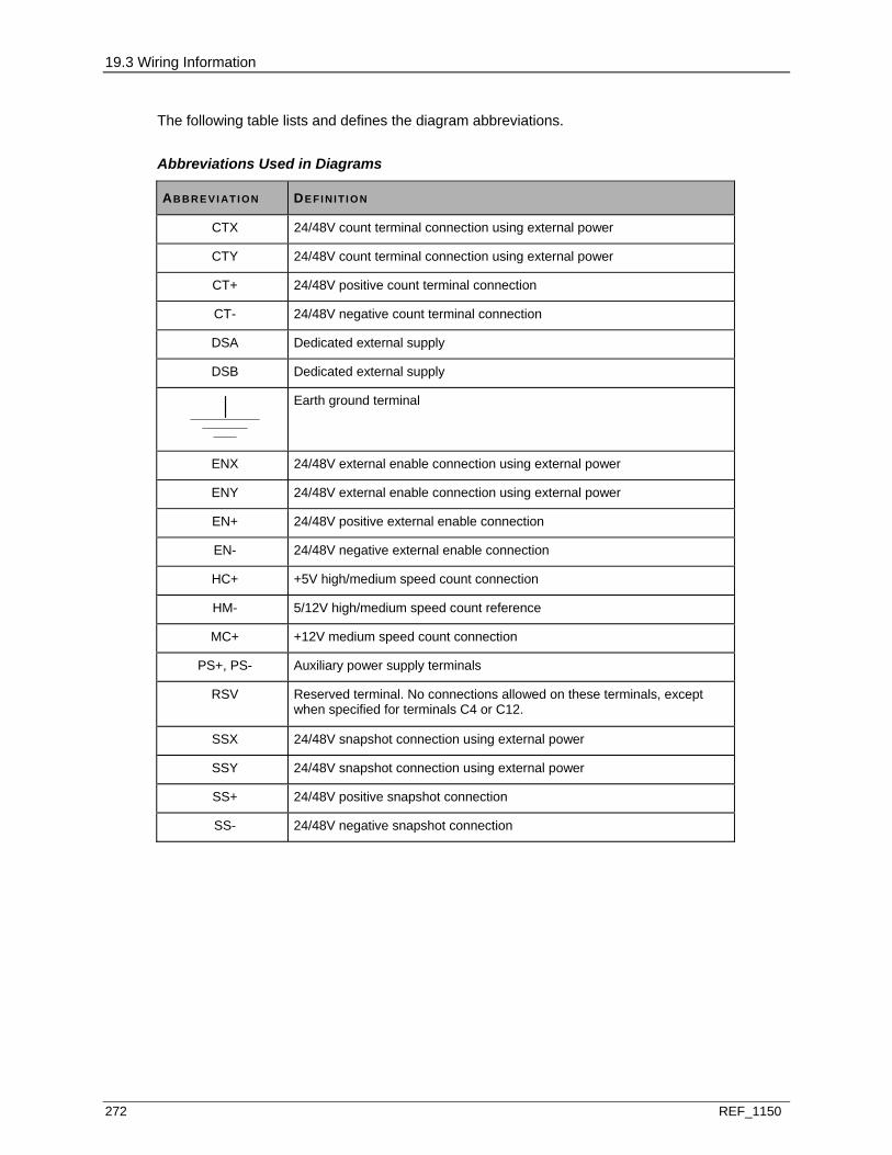
19.3 Wiring Information
272 REF_1150
The following table lists and defines the diagram abbreviations.
Abbreviations Used in Diagrams
AB B R E V I AT I ON DE FI NI T I O N
CTX 24/48V count terminal connection using external power
CTY 24/48V count terminal connection using external power
CT+ 24/48V positive count terminal connection
CT- 24/48V negative count terminal connection
DSA Dedicated external supply
DSB Dedicated external supply
Earth ground terminal
ENX 24/48V external enable connection using external power
ENY 24/48V external enable connection using external power
EN+ 24/48V positive external enable connection
EN- 24/48V negative external enable connection
HC+ +5V high/medium speed count connection
HM- 5/12V high/medium speed count reference
MC+ +12V medium speed count connection
PS+, PS- Auxiliary power supply terminals
RSV Reserved terminal. No connections allowed on these terminals, except when specified for terminals C4 or C12.
SSX 24/48V snapshot connection using external power
SSY 24/48V snapshot connection using external power
SS+ 24/48V positive snapshot connection
SS- 24/48V negative snapshot connection

19.3 Wiring Information
REF_1150 273
19.3.2 PULSE ACCUMULATOR FIELD CONNECTION WIRING DIAGRAMS (NON-CE MARK CERTIFIED)
Figure 107: 5 V Count Field Connections - (Non-CE Mark)
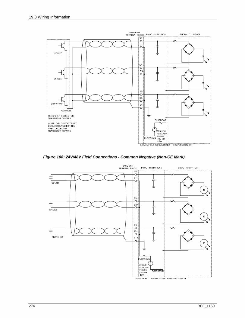
19.3 Wiring Information
274 REF_1150
Figure 108: 24V/48V Field Connections - Common Negative (Non-CE Mark)
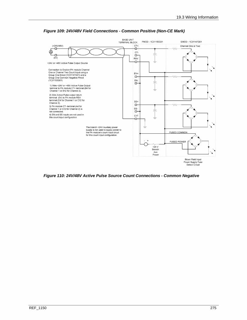
19.3 Wiring Information
REF_1150 275
Figure 109: 24V/48V Field Connections - Common Positive (Non-CE Mark)
Figure 110: 24V/48V Active Pulse Source Count Connections - Common Negative
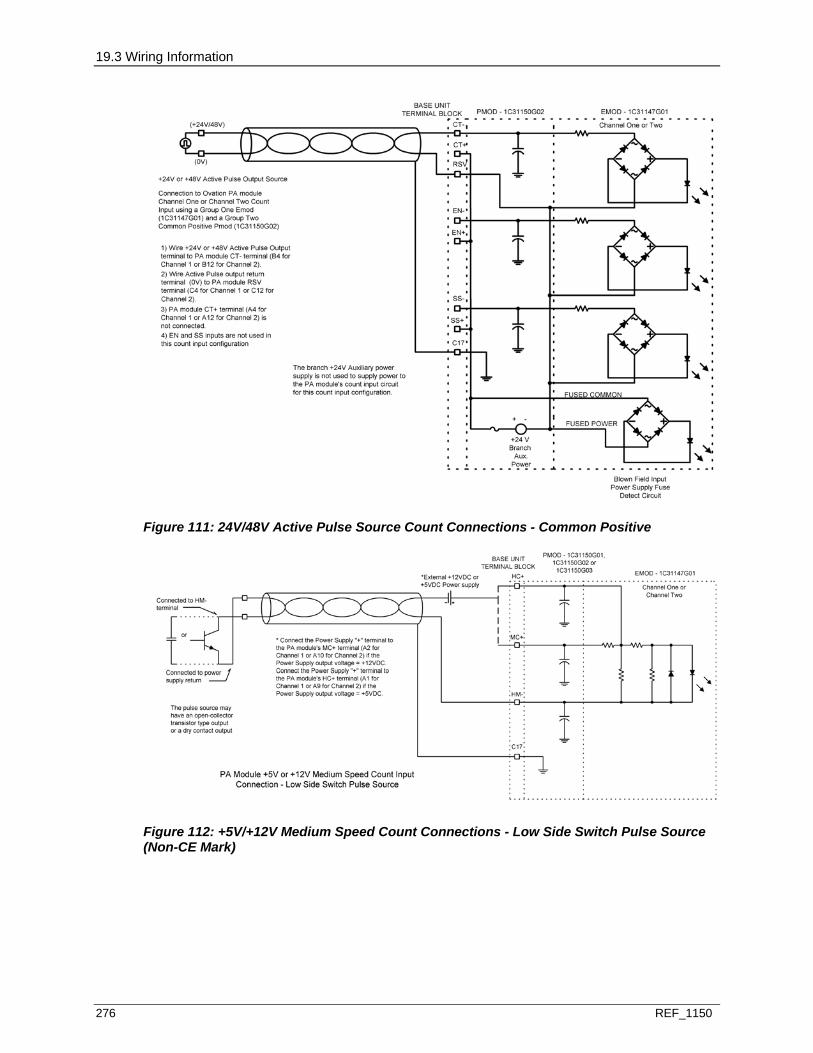
19.3 Wiring Information
276 REF_1150
Figure 111: 24V/48V Active Pulse Source Count Connections - Common Positive
Figure 112: +5V/+12V Medium Speed Count Connections - Low Side Switch Pulse Source (Non-CE Mark)
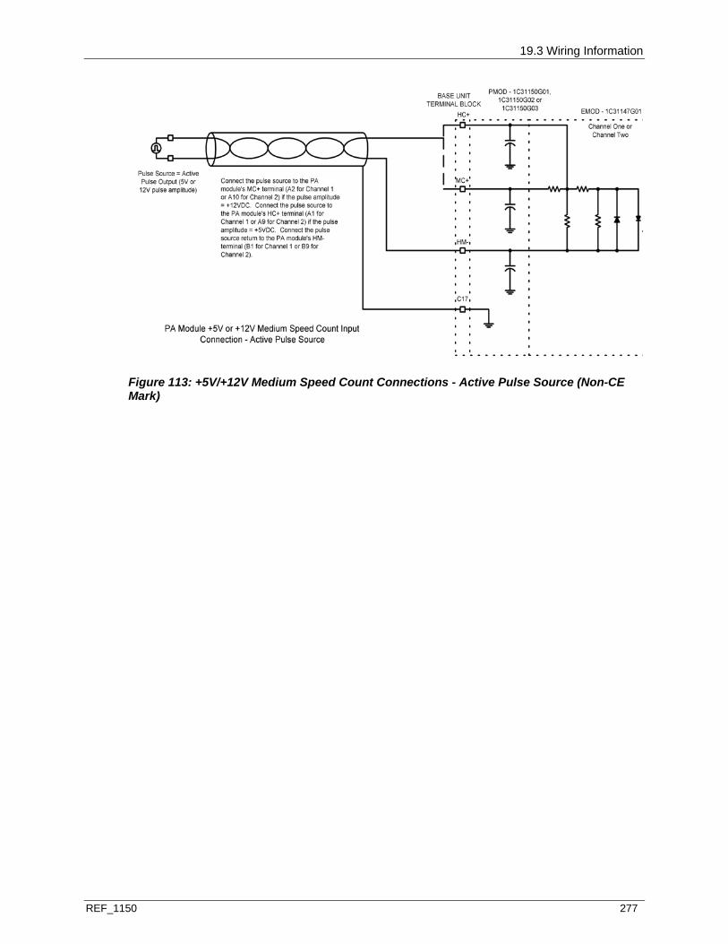
19.3 Wiring Information
REF_1150 277
Figure 113: +5V/+12V Medium Speed Count Connections - Active Pulse Source (Non-CE Mark)
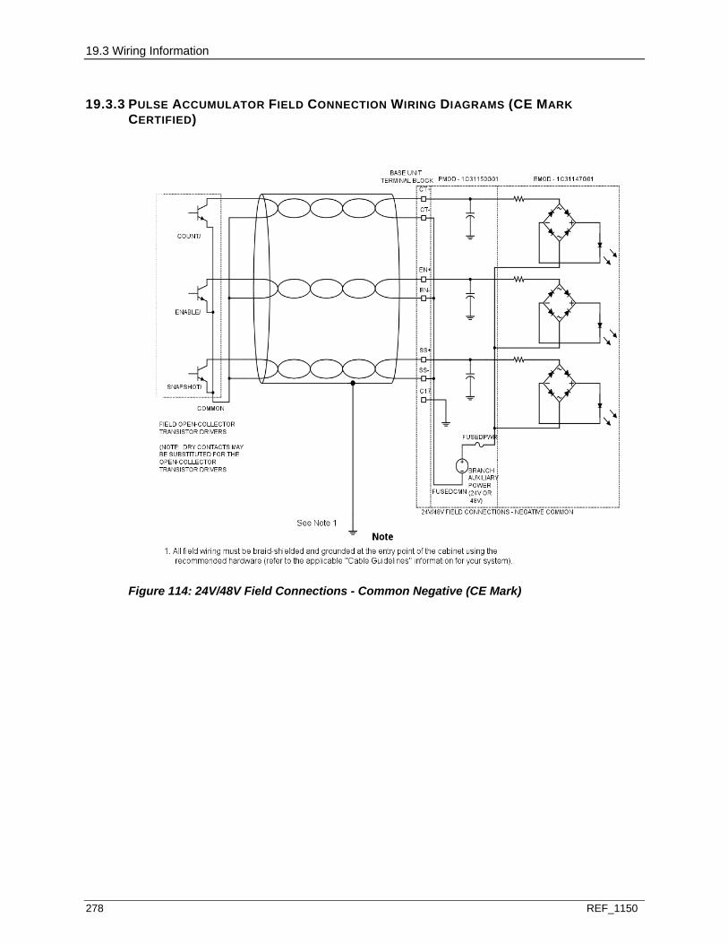
19.3 Wiring Information
278 REF_1150
19.3.3 PULSE ACCUMULATOR FIELD CONNECTION WIRING DIAGRAMS (CE MARK CERTIFIED)
Figure 114: 24V/48V Field Connections - Common Negative (CE Mark)

19.3 Wiring Information
REF_1150 279
Figure 115: 24V/48V Field Connections - Common Positive (CE Mark)

19.3 Wiring Information
280 REF_1150
(refer to applicable "Cable Guidelines" information for your system).
Figure 116: 24V/48V Active Pulse Source Count Connections - Common Negative
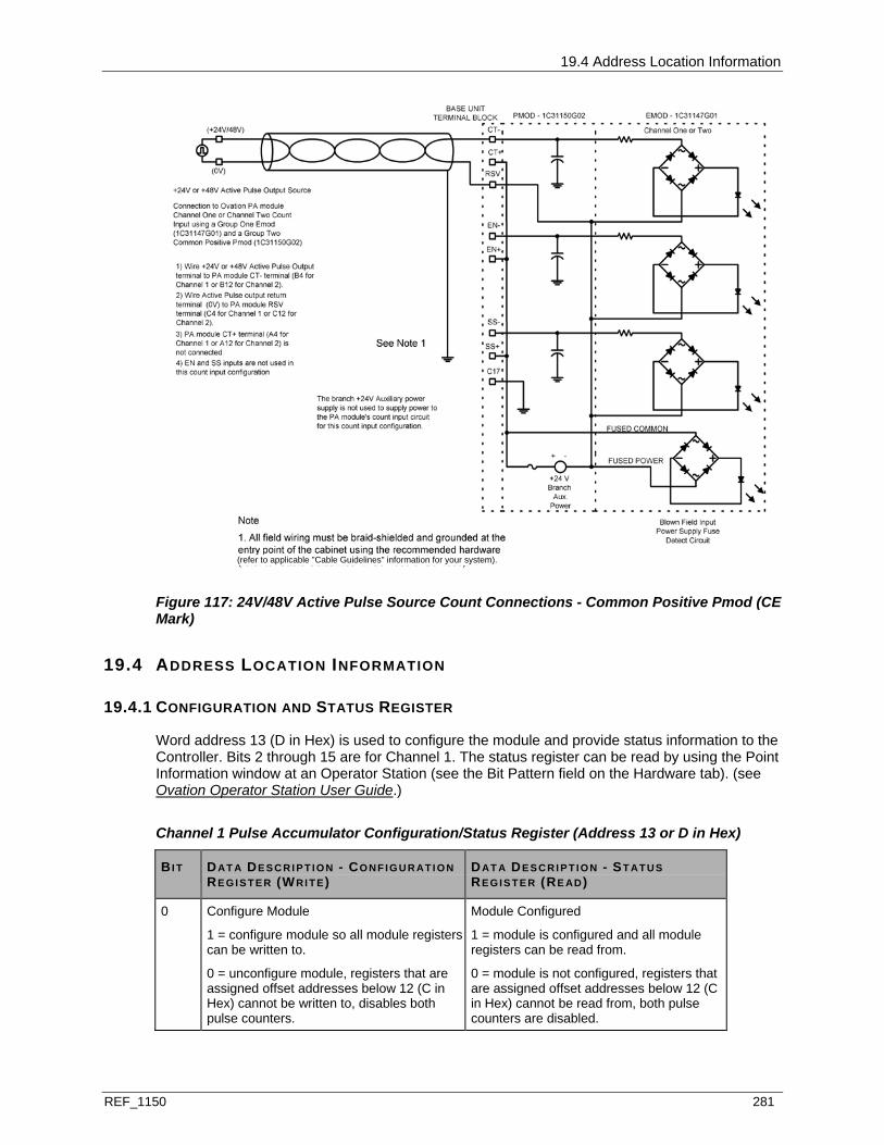
19.4 Address Location Information
REF_1150 281
(refer to applicable "Cable Guidelines" information for your system).
Figure 117: 24V/48V Active Pulse Source Count Connections - Common Positive Pmod (CE Mark)
19.4 ADDRESS LOCATION INFORMATION
19.4.1 CONFIGURATION AND STATUS REGISTER
Word address 13 (D in Hex) is used to configure the module and provide status information to the Controller. Bits 2 through 15 are for Channel 1. The status register can be read by using the Point Information window at an Operator Station (see the Bit Pattern field on the Hardware tab). (see Ovation Operator Station User Guide.)
Channel 1 Pulse Accumulator Configuration/Status Register (Address 13 or D in Hex)
BI T DAT A DE S C R I P T I O N - CO NF I G U R AT I O N RE GI S T E R (WRI T E)
DAT A DE S C R I P T I O N - ST ATUS RE GI S T E R (RE AD)
0 Configure Module
1 = configure module so all module registers can be written to.
0 = unconfigure module, registers that are assigned offset addresses below 12 (C in Hex) cannot be written to, disables both pulse counters.
Module Configured
1 = module is configured and all module registers can be read from.
0 = module is not configured, registers that are assigned offset addresses below 12 (C in Hex) cannot be read from, both pulse counters are disabled.
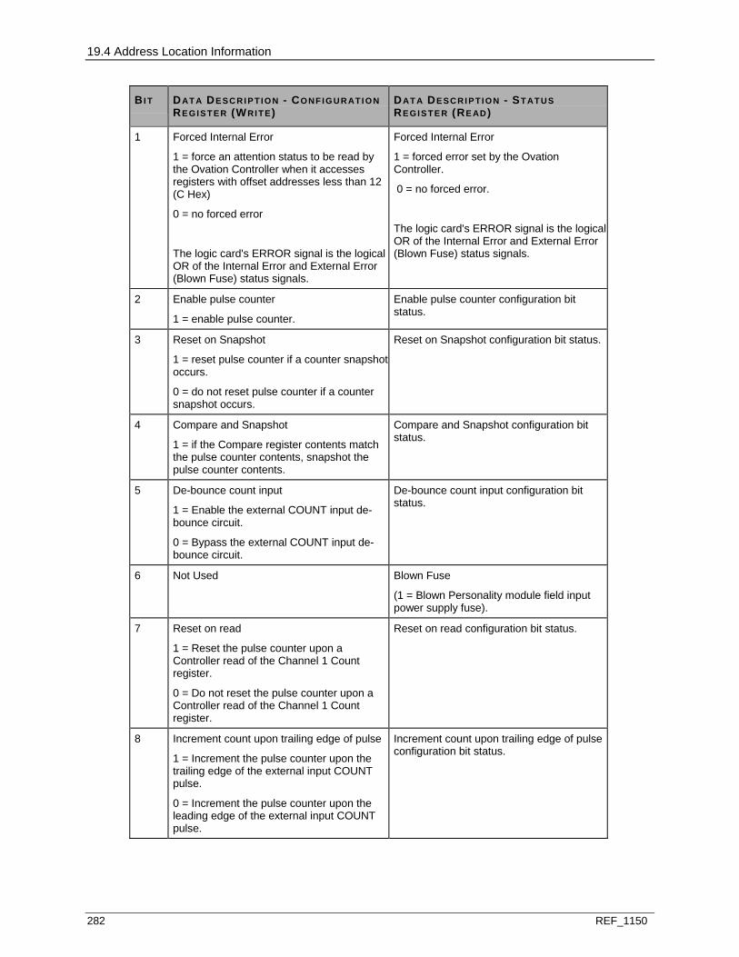
19.4 Address Location Information
282 REF_1150
BI T DAT A DE S C R I P T I O N - CO NF I G U R AT I O N RE GI S T E R (WRI T E)
DAT A DE S C R I P T I O N - ST ATUS RE GI S T E R (RE AD)
1 Forced Internal Error
1 = force an attention status to be read by the Ovation Controller when it accesses registers with offset addresses less than 12 (C Hex)
0 = no forced error
The logic card's ERROR signal is the logical OR of the Internal Error and External Error (Blown Fuse) status signals.
Forced Internal Error
1 = forced error set by the Ovation Controller.
0 = no forced error.
The logic card's ERROR signal is the logical OR of the Internal Error and External Error (Blown Fuse) status signals.
2 Enable pulse counter
1 = enable pulse counter.
Enable pulse counter configuration bit status.
3 Reset on Snapshot
1 = reset pulse counter if a counter snapshot occurs.
0 = do not reset pulse counter if a counter snapshot occurs.
Reset on Snapshot configuration bit status.
4 Compare and Snapshot
1 = if the Compare register contents match the pulse counter contents, snapshot the pulse counter contents.
Compare and Snapshot configuration bit status.
5 De-bounce count input
1 = Enable the external COUNT input de-bounce circuit.
0 = Bypass the external COUNT input de-bounce circuit.
De-bounce count input configuration bit status.
6 Not Used Blown Fuse
(1 = Blown Personality module field input power supply fuse).
7 Reset on read
1 = Reset the pulse counter upon a Controller read of the Channel 1 Count register.
0 = Do not reset the pulse counter upon a Controller read of the Channel 1 Count register.
Reset on read configuration bit status.
8 Increment count upon trailing edge of pulse
1 = Increment the pulse counter upon the trailing edge of the external input COUNT pulse.
0 = Increment the pulse counter upon the leading edge of the external input COUNT pulse.
Increment count upon trailing edge of pulse configuration bit status.
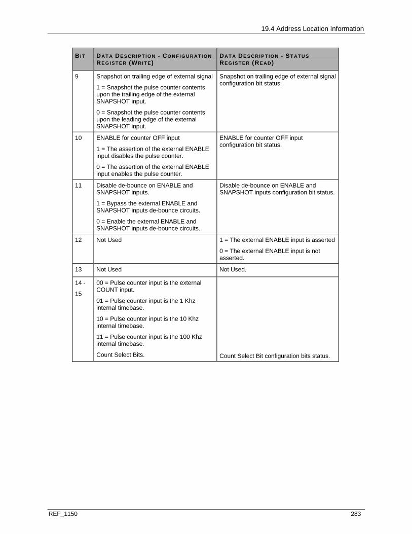
19.4 Address Location Information
REF_1150 283
BI T DAT A DE S C R I P T I O N - CO NF I G U R AT I O N RE GI S T E R (WRI T E)
DAT A DE S C R I P T I O N - ST ATUS RE GI S T E R (RE AD)
9 Snapshot on trailing edge of external signal
1 = Snapshot the pulse counter contents upon the trailing edge of the external SNAPSHOT input.
0 = Snapshot the pulse counter contents upon the leading edge of the external SNAPSHOT input.
Snapshot on trailing edge of external signal configuration bit status.
10 ENABLE for counter OFF input
1 = The assertion of the external ENABLE input disables the pulse counter.
0 = The assertion of the external ENABLE input enables the pulse counter.
ENABLE for counter OFF input configuration bit status.
11 Disable de-bounce on ENABLE and SNAPSHOT inputs.
1 = Bypass the external ENABLE and SNAPSHOT inputs de-bounce circuits.
0 = Enable the external ENABLE and SNAPSHOT inputs de-bounce circuits.
Disable de-bounce on ENABLE and SNAPSHOT inputs configuration bit status.
12 Not Used 1 = The external ENABLE input is asserted
0 = The external ENABLE input is not asserted.
13 Not Used Not Used.
14 -
15
00 = Pulse counter input is the external COUNT input.
01 = Pulse counter input is the 1 Khz internal timebase.
10 = Pulse counter input is the 10 Khz internal timebase.
11 = Pulse counter input is the 100 Khz internal timebase.
Count Select Bits.
Count Select Bit configuration bits status.
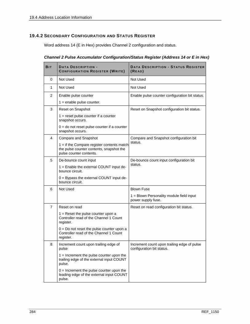
19.4 Address Location Information
284 REF_1150
19.4.2 SECONDARY CONFIGURATION AND STATUS REGISTER
Word address 14 (E in Hex) provides Channel 2 configuration and status.
Channel 2 Pulse Accumulator Configuration/Status Register (Address 14 or E in Hex)
BI T DAT A DE S C R I P T I O N - CO N FI G U R AT I O N REGI S TE R (WRI TE)
DAT A DE S C R I P T I O N - ST ATUS REGI S TER (RE AD)
0 Not Used Not Used
1 Not Used Not Used
2 Enable pulse counter
1 = enable pulse counter.
Enable pulse counter configuration bit status.
3 Reset on Snapshot
1 = reset pulse counter if a counter snapshot occurs.
0 = do not reset pulse counter if a counter snapshot occurs.
Reset on Snapshot configuration bit status.
4 Compare and Snapshot
1 = if the Compare register contents match the pulse counter contents, snapshot the pulse counter contents.
Compare and Snapshot configuration bit status.
5 De-bounce count input
1 = Enable the external COUNT input de-bounce circuit.
0 = Bypass the external COUNT input de-bounce circuit.
De-bounce count input configuration bit status.
6 Not Used Blown Fuse
1 = Blown Personality module field input power supply fuse.
7 Reset on read
1 = Reset the pulse counter upon a Controller read of the Channel 1 Count register.
0 = Do not reset the pulse counter upon a Controller read of the Channel 1 Count register.
Reset on read configuration bit status.
8 Increment count upon trailing edge of pulse
1 = Increment the pulse counter upon the trailing edge of the external input COUNT pulse.
0 = Increment the pulse counter upon the leading edge of the external input COUNT pulse.
Increment count upon trailing edge of pulse configuration bit status.

19.4 Address Location Information
REF_1150 285
BI T DAT A DE S C R I P T I O N - CO N FI G U R AT I O N REGI S TE R (WRI TE)
DAT A DE S C R I P T I O N - ST ATUS REGI S TER (RE AD)
9 Snapshot on trailing edge of external signal
1 = Snapshot the pulse counter contents upon the trailing edge of the external SNAPSHOT input.
0 = Snapshot the pulse counter contents upon the leading edge of the external SNAPSHOT input.
Snapshot on trailing edge of external signal configuration bit status.
10 ENABLE for counter OFF input
1 = The assertion of the external ENABLE input disables the pulse counter.
0 = The assertion of the external ENABLE input enables the pulse counter.
ENABLE for counter OFF input configuration bit status.
11 Disable de-bounce on ENABLE and SNAPSHOT inputs
1 = Bypass the external ENABLE and SNAPSHOT inputs de-bounce circuits.
0 = Enable the external ENABLE and SNAPSHOT inputs de-bounce circuits.
Disable de-bounce on ENABLE and SNAPSHOT inputs configuration bit status.
12 Not Used 1 = The external ENABLE input is asserted.
0 = The external ENABLE input is not asserted.
13 Not Used Not Used
14 - 15
00 = Pulse counter input is the external COUNT input.
01 = Pulse counter input is the 1 Khz internal timebase.
10 = Pulse counter input is the 10 Khz internal timebase.
11 = Pulse counter input is the 100 Khz internal timebase.
Count Select Bits.
Count Select Bit configuration bits status
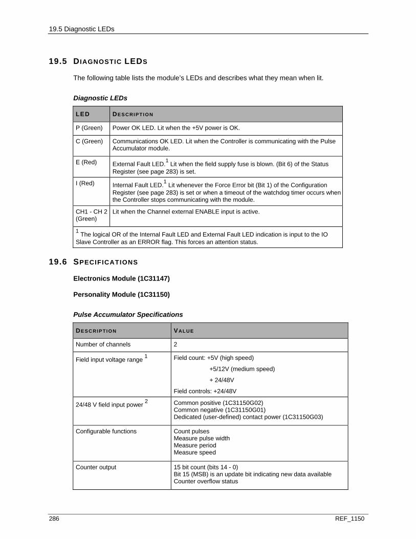
19.5 Diagnostic LEDs
286 REF_1150
19.5 DIAGNOSTIC LEDS
The following table lists the module’s LEDs and describes what they mean when lit.
Diagnostic LEDs
LED DE S C RI P TI O N
P (Green) Power OK LED. Lit when the +5V power is OK.
C (Green) Communications OK LED. Lit when the Controller is communicating with the Pulse Accumulator module.
E (Red) External Fault LED.1 Lit when the field supply fuse is blown. (Bit 6) of the Status Register (see page 283) is set.
I (Red) Internal Fault LED.1 Lit whenever the Force Error bit (Bit 1) of the Configuration Register (see page 283) is set or when a timeout of the watchdog timer occurs when the Controller stops communicating with the module.
CH1 - CH 2 (Green)
Lit when the Channel external ENABLE input is active.
1 The logical OR of the Internal Fault LED and External Fault LED indication is input to the IO Slave Controller as an ERROR flag. This forces an attention status.
19.6 SPECIFICATIONS
Electronics Module (1C31147)
Personality Module (1C31150)
Pulse Accumulator Specifications
DE S C RI P TI O N VALUE
Number of channels 2
Field input voltage range 1 Field count: +5V (high speed)
+5/12V (medium speed)
+ 24/48V
Field controls: +24/48V
24/48 V field input power 2 Common positive (1C31150G02) Common negative (1C31150G01) Dedicated (user-defined) contact power (1C31150G03)
Configurable functions Count pulses Measure pulse width Measure period Measure speed
Counter output 15 bit count (bits 14 - 0) Bit 15 (MSB) is an update bit indicating new data available Counter overflow status
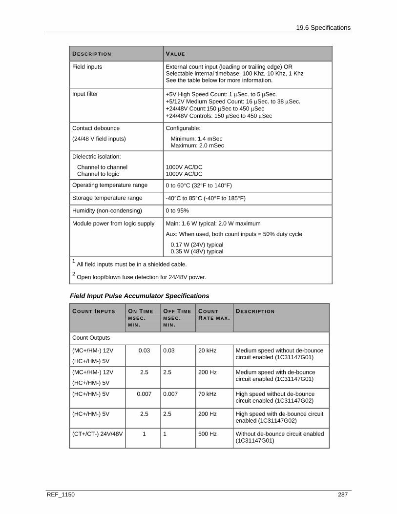
19.6 Specifications
REF_1150 287
DE S C RI P TI O N VALUE
Field inputs External count input (leading or trailing edge) OR Selectable internal timebase: 100 Khz, 10 Khz, 1 Khz See the table below for more information.
Input filter +5V High Speed Count: 1 μSec. to 5 μSec. +5/12V Medium Speed Count: 16 μSec. to 38 μSec. +24/48V Count:150 μSec to 450 μSec +24/48V Controls: 150 μSec to 450 μSec
Contact debounce
(24/48 V field inputs)
Configurable:
Minimum: 1.4 mSec Maximum: 2.0 mSec
Dielectric isolation:
Channel to channel Channel to logic
1000V AC/DC 1000V AC/DC
Operating temperature range 0 to 60°C (32°F to 140°F)
Storage temperature range -40°C to 85°C (-40°F to 185°F)
Humidity (non-condensing) 0 to 95%
Module power from logic supply Main: 1.6 W typical: 2.0 W maximum
Aux: When used, both count inputs = 50% duty cycle
0.17 W (24V) typical 0.35 W (48V) typical
1 All field inputs must be in a shielded cable. 2 Open loop/blown fuse detection for 24/48V power.
Field Input Pulse Accumulator Specifications
CO U N T IN P U TS ON TI M E M SE C. M I N.
OF F T IM E M SE C. M I N.
CO U N T RATE M AX.
DE S C RI P TI O N
Count Outputs
(MC+/HM-) 12V
(HC+/HM-) 5V
0.03 0.03 20 kHz Medium speed without de-bounce circuit enabled (1C31147G01)
(MC+/HM-) 12V
(HC+/HM-) 5V
2.5 2.5 200 Hz Medium speed with de-bounce circuit enabled (1C31147G01)
(HC+/HM-) 5V 0.007 0.007 70 kHz High speed without de-bounce circuit enabled (1C31147G02)
(HC+/HM-) 5V 2.5 2.5 200 Hz High speed with de-bounce circuit enabled (1C31147G02)
(CT+/CT-) 24V/48V 1 1 500 Hz Without de-bounce circuit enabled(1C31147G01)
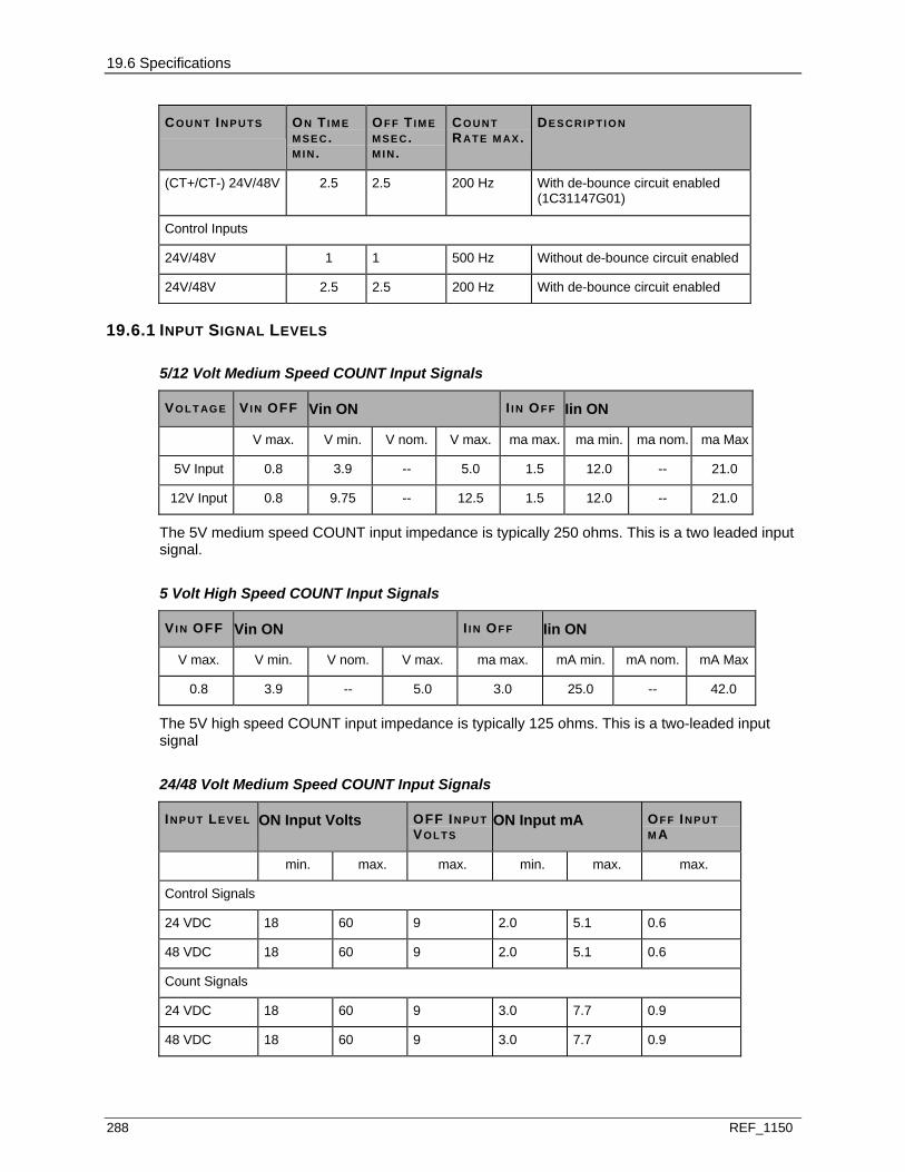
19.6 Specifications
288 REF_1150
CO U N T IN P U TS ON TI M E M SE C. M I N.
OF F T IM E M SE C. M I N.
CO U N T RATE M AX.
DE S C RI P TI O N
(CT+/CT-) 24V/48V 2.5 2.5 200 Hz With de-bounce circuit enabled (1C31147G01)
Control Inputs
24V/48V 1 1 500 Hz Without de-bounce circuit enabled
24V/48V 2.5 2.5 200 Hz With de-bounce circuit enabled
19.6.1 INPUT SIGNAL LEVELS
5/12 Volt Medium Speed COUNT Input Signals
VO L T AG E VI N OFF Vin ON I I N OF F Iin ON
V max. V min. V nom. V max. ma max. ma min. ma nom. ma Max
5V Input 0.8 3.9 -- 5.0 1.5 12.0 -- 21.0
12V Input 0.8 9.75 -- 12.5 1.5 12.0 -- 21.0
The 5V medium speed COUNT input impedance is typically 250 ohms. This is a two leaded input signal.
5 Volt High Speed COUNT Input Signals
VI N OFF Vin ON I I N OF F Iin ON
V max. V min. V nom. V max. ma max. mA min. mA nom. mA Max
0.8 3.9 -- 5.0 3.0 25.0 -- 42.0
The 5V high speed COUNT input impedance is typically 125 ohms. This is a two-leaded input signal
24/48 Volt Medium Speed COUNT Input Signals
IN P U T LE VE L ON Input Volts OFF IN P U T VO L TS
ON Input mA OF F INP UT M A
min. max. max. min. max. max.
Control Signals
24 VDC 18 60 9 2.0 5.1 0.6
48 VDC 18 60 9 2.0 5.1 0.6
Count Signals
24 VDC 18 60 9 3.0 7.7 0.9
48 VDC 18 60 9 3.0 7.7 0.9

19.6 Specifications
REF_1150 289
This signal level applies to the control inputs and to the 24/48 Volt COUNT input depending upon the group and the wiring.
This input accepts either a 24V or 48V input. The Electronics Module accepts a positive or a negative field signal common. The Personality Module determines if the field signal common is positive or negative.

REF_1150 291
IN THIS SECTION
Description ......................................................................................................................291 Module Group Information ..............................................................................................291 Module Specific Information............................................................................................293 Wiring Information ...........................................................................................................295 Address Location Information .........................................................................................301 Diagnostic LEDs..............................................................................................................302 Specifications ..................................................................................................................303
20.1 DESCRIPTION
An Ovation Relay Output module consists of an Electronics module, a base assembly, and relays. The Relay Output module provides a means to switch high AC voltages at high currents to field devices. There are two versions of the Relay Output base assembly which contain either 12 or 16 relays within each base. The 12 Relay Output base assembly provides the additional advantage of being able to switch larger DC voltages at high currents.
Each Relay Output base assembly incorporates an integral Relay Output Electronics module to interface between the relays and the Ovation I/O Controller. The Relay Output Electronics module provides configurable communication timeout periods and LEDs to indicate the status of each output.
The Relay Output module is applicable for CE Mark certified systems.
Note: I/O Module General Information (see page 15) contains environmental, installation, wiring, and fuse information for I/O modules.
20.2 MODULE GROUP INFORMATION
20.2.1 ELECTRONIC MODULE (EMOD)
There is one Electronics module group for the Relay Output module:
1C31219G01 provides an interface between the Ovation Controller and the mechanical relays that are used to switch high AC voltages at high currents. This module plugs into the Relay Output base assembly.
Note: The Relay Output base assembly does not incorporate a Personality module.
S E C T I O N 2 0
RELAY OUTPUT MODULE
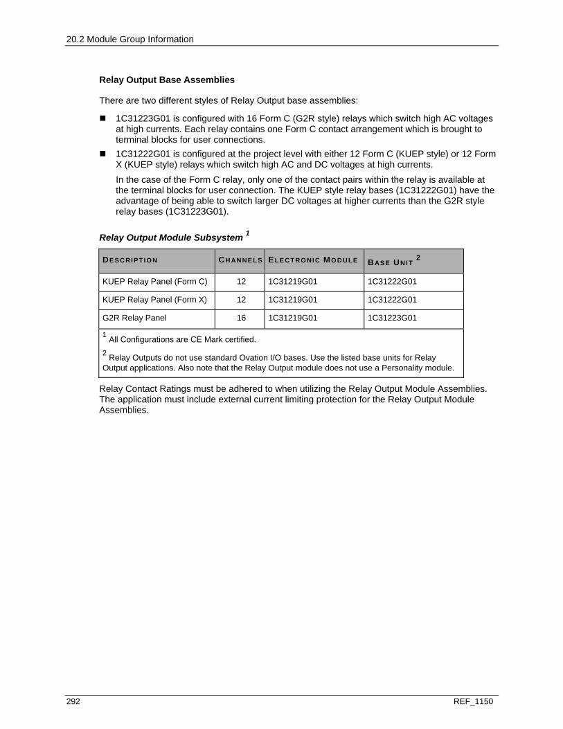
20.2 Module Group Information
292 REF_1150
Relay Output Base Assemblies
There are two different styles of Relay Output base assemblies:
1C31223G01 is configured with 16 Form C (G2R style) relays which switch high AC voltages at high currents. Each relay contains one Form C contact arrangement which is brought to terminal blocks for user connections.
1C31222G01 is configured at the project level with either 12 Form C (KUEP style) or 12 Form X (KUEP style) relays which switch high AC and DC voltages at high currents. In the case of the Form C relay, only one of the contact pairs within the relay is available at the terminal blocks for user connection. The KUEP style relay bases (1C31222G01) have the advantage of being able to switch larger DC voltages at higher currents than the G2R style relay bases (1C31223G01).
Relay Output Module Subsystem 1
DE S C RI P TI O N CH AN N E L S EL E CT RO NI C MO D U LE BAS E UNI T 2
KUEP Relay Panel (Form C) 12 1C31219G01 1C31222G01
KUEP Relay Panel (Form X) 12 1C31219G01 1C31222G01
G2R Relay Panel 16 1C31219G01 1C31223G01
1 All Configurations are CE Mark certified. 2 Relay Outputs do not use standard Ovation I/O bases. Use the listed base units for Relay Output applications. Also note that the Relay Output module does not use a Personality module.
Relay Contact Ratings must be adhered to when utilizing the Relay Output Module Assemblies. The application must include external current limiting protection for the Relay Output Module Assemblies.
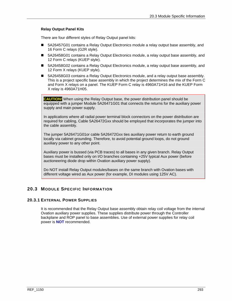
20.3 Module Specific Information
REF_1150 293
Relay Output Panel Kits
There are four different styles of Relay Output panel kits:
5A26457G01 contains a Relay Output Electronics module a relay output base assembly, and 16 Form C relays (G2R style).
5A26458G01 contains a Relay Output Electronics module, a relay output base assembly, and 12 Form C relays (KUEP style).
5A26458G02 contains a Relay Output Electronics module, a relay output base assembly, and 12 Form X relays (KUEP style).
5A26458G03 contains a Relay Output Electronics module, and a relay output base assembly. This is a project specific base assembly in which the project determines the mix of the Form C and Form X relays on a panel. The KUEP Form C relay is 4960A71H16 and the KUEP Form X relay is 4960A71H05.
CAUTION! When using the Relay Output base, the power distribution panel should be equipped with a jumper Module 5A26471G01 that connects the returns for the auxiliary power supply and main power supply.
In applications where all radial power terminal block connectors on the power distribution are required for cabling, Cable 5A26472Gxx should be employed that incorporates the jumper into the cable assembly.
The jumper 5A26471G01or cable 5A26472Gxx ties auxiliary power return to earth ground locally via cabinet grounding. Therefore, to avoid potential ground loops, do not ground auxiliary power to any other point.
Auxiliary power is bussed (via PCB traces) to all bases in any given branch. Relay Output bases must be installed only on I/O branches containing +25V typical Aux power (before auctioneering diode drop within Ovation auxiliary power supply).
Do NOT install Relay Output modules/bases on the same branch with Ovation bases with different voltage wired as Aux power (for example, DI modules using 125V AC).
20.3 MODULE SPECIFIC INFORMATION
20.3.1 EXTERNAL POWER SUPPLIES
It is recommended that the Relay Output base assembly obtain relay coil voltage from the internal Ovation auxiliary power supplies. These supplies distribute power through the Controller backplane and ROP panel to base assemblies. Use of external power supplies for relay coil power is NOT recommended.
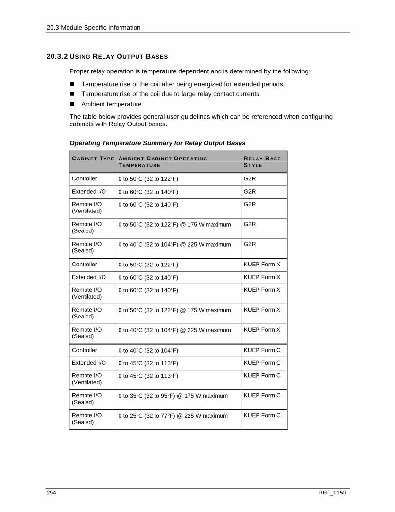
20.3 Module Specific Information
294 REF_1150
20.3.2 USING RELAY OUTPUT BASES
Proper relay operation is temperature dependent and is determined by the following:
Temperature rise of the coil after being energized for extended periods. Temperature rise of the coil due to large relay contact currents. Ambient temperature.
The table below provides general user guidelines which can be referenced when configuring cabinets with Relay Output bases.
Operating Temperature Summary for Relay Output Bases
CABI NE T TY PE AM BI E NT CABI NE T OP E R AT I NG TEM PER AT UR E
RE L AY BAS E ST Y L E
Controller 0 to 50°C (32 to 122°F) G2R
Extended I/O 0 to 60°C (32 to 140°F) G2R
Remote I/O (Ventilated)
0 to 60°C (32 to 140°F) G2R
Remote I/O (Sealed)
0 to 50°C (32 to 122°F) @ 175 W maximum G2R
Remote I/O (Sealed)
0 to 40°C (32 to 104°F) @ 225 W maximum G2R
Controller 0 to 50°C (32 to 122°F) KUEP Form X
Extended I/O 0 to 60°C (32 to 140°F) KUEP Form X
Remote I/O (Ventilated)
0 to 60°C (32 to 140°F) KUEP Form X
Remote I/O (Sealed)
0 to 50°C (32 to 122°F) @ 175 W maximum KUEP Form X
Remote I/O (Sealed)
0 to 40°C (32 to 104°F) @ 225 W maximum KUEP Form X
Controller 0 to 40°C (32 to 104°F) KUEP Form C
Extended I/O 0 to 45°C (32 to 113°F) KUEP Form C
Remote I/O (Ventilated)
0 to 45°C (32 to 113°F) KUEP Form C
Remote I/O (Sealed)
0 to 35°C (32 to 95°F) @ 175 W maximum KUEP Form C
Remote I/O (Sealed)
0 to 25°C (32 to 77°F) @ 225 W maximum KUEP Form C

20.4 Wiring Information
REF_1150 295
20.3.3 BLOWN FUSE DETECTION CIRCUIT
Bit 6 in the status register enables the Controller to monitor the status of the field supply fuse, and it gives a visual indication of the status via the “EXTERNAL ERROR (see page 302)” LED.
The Controller enables this feature by writing a “1” to Bit 7 of the configuration register. If enabled and the field supply voltage is between 18VDC and 25.5VDC, the circuit indicates the field supply fuse is OK by turning OFF the “EXTERNAL ERROR” LED and clearing Bit 6 of the module status register. If enabled and the field supply voltage is less than 0.4VDC, the circuit indicates the field supply fuse is blown by turning ON the “EXTERNAL ERROR” LED and setting Bit 6 of the module status register.
In summary, this feature is specified to operate as follows:
18VDC < Field supply voltage < 25.5VDC => Fuse is OK 0.4VDC < Field supply voltage < 18VDC => UNDEFINED Field supply voltage < 0.4VDC => Fuse is blown After a powering reset, the blown fuse detection circuit is disabled.
20.4 WIRING INFORMATION
20.4.1 RELAY OUTPUT TERMINAL BLOCK WIRING INFORMATION
Each relay base assembly employs terminal blocks which are permanently marked with appropriate relay contact designations at each position. The terminal block marking indicates how field wiring is connected to each terminal block position in the respective relay base assemblies.
The terminal block markings for the G2R style relay output base assembly and for the KUEP style Relay Output base assemblies are illustrated below. The following table lists and defines the abbreviations used in those diagrams.
NC
TB1
NO C N
CTB3
NO C N
CTB5
NO C N
CTB7
NO C N
CTB9
NO C N
CTB11
NO C N
CTB13
NO C N
CTB15
NO C
NC
TB2
NO C N
CTB4
NO C N
CTB6
NO C N
CTB8
NO C N
CTB10
NO C N
CTB12
NO C N
CTB14
NO C N
CTB16
NO C
Figure 118: Terminal Block Connections for the G2R Relay Output Base Assembly
Form C Relays Installed
NO
TB1
NC C N
OTB2
NC C N
OTB3
NC C N
OTB4
NC C N
OTB5
NC C N
OTB6
NC C N
OTB7
NC C N
OTB8
NC C N
OTB9
NC C N
OTB
10
NC C N
OTB11
NC C N
OTB12
NC C
NO
TB1
C NO
TB2
C NO
TB3
C NO
TB4
C NO
TB5
C NO
TB6
C NO
TB7
C NO
TB8
C NO
TB9
C NO
TB
10C N
OTB11
C NO
TB12
C
Form X Relays Installed
Figure 119: Terminal Block Connections for the KUEP Relay Output Base Assembly

20.4 Wiring Information
296 REF_1150
Abbreviations Used in Diagrams
AB B R E V I AT I ON DE FI NI T I O N
NC 1 Normally Closed contact connection
NO Normally Open contact connection
C Common contact connection
1 Do NOT use the NC terminal position when using the KUEP style base assembly with a Form X style relay inserted. The terminal position should remain unconnected.
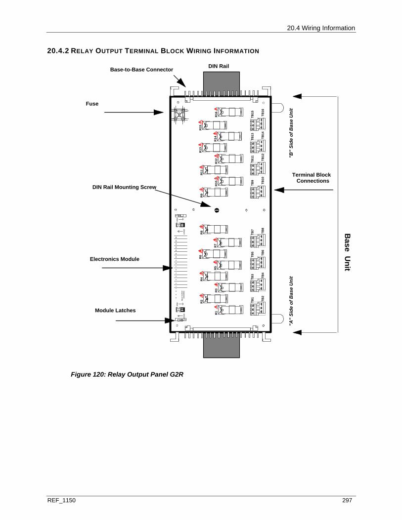
20.4 Wiring Information
REF_1150 297
20.4.2 RELAY OUTPUT TERMINAL BLOCK WIRING INFORMATION
DIN Rail
DIN Rail Mounting Screw
Base-to-Base Connector
Base U
nit
Module Latches
R7
R6
R5
R4
R3
R2
R1
R8
R15
R14
R13
R12
R11
R10
R9
R16
TB1
Electronics Module
Fuse
Terminal BlockConnections
"A"
Side
of B
ase
Uni
t"B
" Si
de o
f Bas
e U
nit
LOC
KED
OPE
NP
CE
I2
34
56
78
910
1112
1314
1516
REL
AY
OU
TPU
T
1C31
219G
01LO
CK
ED
OPE
N1
TB2
TB3
TB4
TB5
TB6
TB7
TB8
TB9
TB10
TB11
TB12
TB13
TB14
TB15
TB16
Figure 120: Relay Output Panel G2R

20.4 Wiring Information
298 REF_1150
DIN Rail
DIN Rail Mounting Screw
Base-to-Base ConnectorB
ase Unit
Module Latches
Electronics Module
Fuse
Terminal BlockConnections
"A"
Side
of B
ase
Uni
t"B
" Si
de o
f Bas
e U
nit
LOC
KED
OPE
NP
CE
I2
34
56
78
910
1112
1314
1516
REL
AY
OU
TPU
T
1C31
219G
01LO
CK
ED
OPE
N
R1R
2
R3
R4
R6
R5
R8
R7
R9
R10
R12
R11
T B 1
T B 2
T B 3
T B 4
T B 5
T B 6
T B 7
T B 8
T B 9
T B 10
T B 11
T B 12
1
Figure 121: Relay Output KUEP
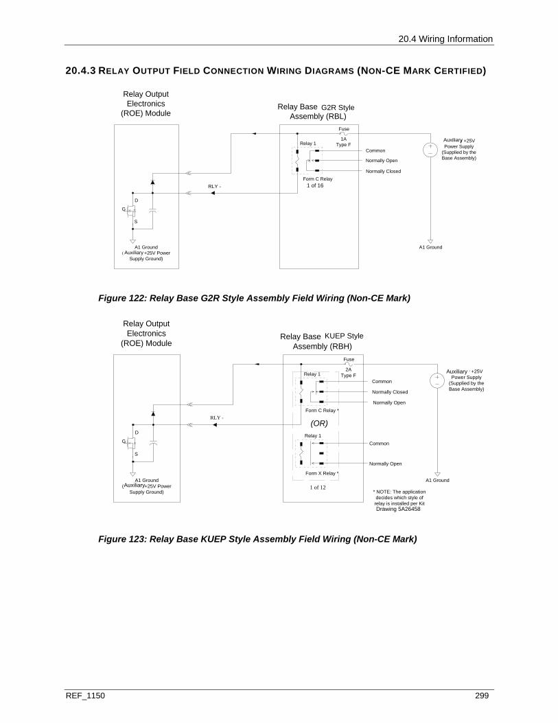
20.4 Wiring Information
REF_1150 299
20.4.3 RELAY OUTPUT FIELD CONNECTION WIRING DIAGRAMS (NON-CE MARK CERTIFIED)
Auxilliary +25VPower Supply
(Supplied by theBase Assembly)
Fuse
RLY1-
FUSEDWET+
Relay OutputElectronics
(ROE) Module
A1 Ground(Auxilliary +25V Power
Supply Ground)
Relay Base Low PowerAssembly (RBL)
1AType F
Normally Open
Normally Closed
Common
Form C Relay
Relay 1
A1 Ground
G
D
S
G2R Style
1 of 16RLY -
Auxiliary
Auxiliary
Figure 122: Relay Base G2R Style Assembly Field Wiring (Non-CE Mark)
KUEP Style
Auxilliary +25VPower Supply
(Supplied by theBase Assembly)
Fuse
RLY1-
FUSEDWET+
Relay OutputElectronics
(ROE) Module
A1 Ground(Auxilliary +25V Power
Supply Ground)
Relay Base High PowerAssembly (RBH)
2AType F
Normally Open
Normally Closed
Common
Form C Relay *
Relay 1
Relay 1
Form X Relay *
* NOTE: The applicationdecides which style of
relay is installed per KitDrwaing 5Axxxx
A1 Ground
Common
Normally Open
(OR)
G
D
S
KUEP Style
Drawing 5A26458
1 of 12
RLY -
Auxiliary
Auxiliary
Figure 123: Relay Base KUEP Style Assembly Field Wiring (Non-CE Mark)
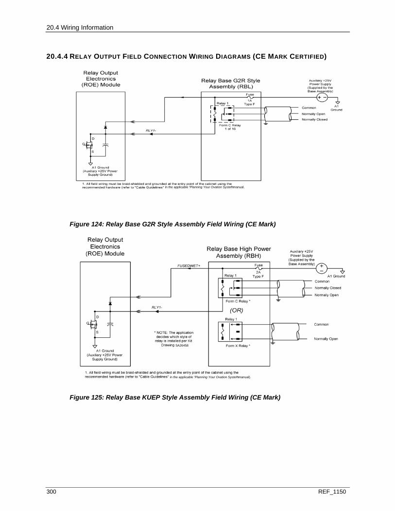
20.4 Wiring Information
300 REF_1150
20.4.4 RELAY OUTPUT FIELD CONNECTION WIRING DIAGRAMS (CE MARK CERTIFIED)
in the applicable "Planning Your Ovation System" manual.
Figure 124: Relay Base G2R Style Assembly Field Wiring (CE Mark)
in the applicable "Planning Your Ovation System" manual).
5A26458
Figure 125: Relay Base KUEP Style Assembly Field Wiring (CE Mark)
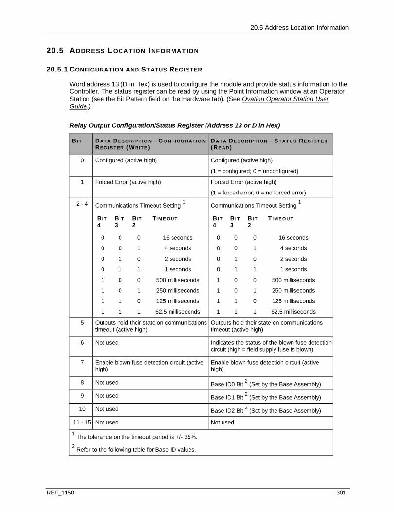
20.5 Address Location Information
REF_1150 301
20.5 ADDRESS LOCATION INFORMATION
20.5.1 CONFIGURATION AND STATUS REGISTER
Word address 13 (D in Hex) is used to configure the module and provide status information to the Controller. The status register can be read by using the Point Information window at an Operator Station (see the Bit Pattern field on the Hardware tab). (See Ovation Operator Station User Guide.)
Relay Output Configuration/Status Register (Address 13 or D in Hex)
BI T DAT A DE S C R I P T I O N - CO NF I G U R AT I O N RE GI S T E R (WRI T E)
DAT A DE S C R I P T I O N - ST ATUS REGI S TER (RE AD)
0 Configured (active high) Configured (active high)
(1 = configured; 0 = unconfigured)
1 Forced Error (active high) Forced Error (active high)
(1 = forced error; 0 = no forced error)
2 - 4 Communications Timeout Setting 1
BI T 4
BI T 3
BI T 2
T I M EO U T
0 0 0 16 seconds
0 0 1 4 seconds
0 1 0 2 seconds
0 1 1 1 seconds
1 0 0 500 milliseconds
1 0 1 250 milliseconds
1 1 0 125 milliseconds
1 1 1 62.5 milliseconds
Communications Timeout Setting 1
BI T 4
BI T 3
BI T 2
T I M EO U T
0 0 0 16 seconds
0 0 1 4 seconds
0 1 0 2 seconds
0 1 1 1 seconds
1 0 0 500 milliseconds
1 0 1 250 milliseconds
1 1 0 125 milliseconds
1 1 1 62.5 milliseconds 5 Outputs hold their state on communications
timeout (active high) Outputs hold their state on communications timeout (active high)
6 Not used Indicates the status of the blown fuse detection circuit (high = field supply fuse is blown)
7 Enable blown fuse detection circuit (active high)
Enable blown fuse detection circuit (active high)
8 Not used Base ID0 Bit 2 (Set by the Base Assembly)
9 Not used Base ID1 Bit 2 (Set by the Base Assembly)
10 Not used Base ID2 Bit 2 (Set by the Base Assembly)
11 - 15 Not used Not used
1 The tolerance on the timeout period is +/- 35%. 2 Refer to the following table for Base ID values.
20.6 Diagnostic LEDs
302 REF_1150
Bit 0: When Bit 0 is set, the module is configured. The Controller configures the module by writing a “1” to Bit 0 of the configuration register. Once configured, it remains configured until a power-up/down reset is generated. After a power-up condition the configuration register clears.
Bit 1: When Bit 1 is set, the internal error LED is turned on and data registers can be written but not read.
Bits 2-4: These bits are used to select the communication timeout period.
Bit 5: When Bit 5 is set, the digital outputs hold their last state on a communications watchdog timeout. When Bit 5 is cleared, the digital outputs are cleared (output transistor is shut off) on a communications watchdog timeout.
Bit 6: This bit indicates the status of the blown fuse detection circuit. When Bit 6 of the status register is set, the field supply fuse is blown (see page 295).
Bit 7: When Bit 7 is set, the blown fuse detection circuit is enabled.
Bits 8-10: The Base Assembly (KUEP or G2R style) straps three bits in hardware which identify which type of base the ROE is plugged into. The type of base can therefore be determined from reading these bits.
Bits 11-15: Not used.
Relay Output Base ID Bits
BI T 10 (BAS E ID2)
BI T 9 (BAS E ID1)
BI T 8 (BAS E ID0) BAS E TYP E
0 0 0 KUEP Style
0 0 1 G2R Style
All others All others All others Reserved for Future Use
20.6 DIAGNOSTIC LEDS
The following table lists the module’s LEDs and describes what they mean when lit.
Relay Output Diagnostic LEDs
LED DE S C RI P TI O N
P (Green) Power OK LED. Lit when the +5V power is OK.
C (Green) Communications OK LED. Lit when the Controller is communicating with the module.
E (Red) External Fault LED. Lit when the field supply fuse is blown and the blown fuse detection circuit is enabled. Blown Fuse bit (Bit 7) of the Configuration Register (see page 301) enables or disables the fuse detection circuit (high = enabled).
I (Red) Internal Fault LED. Lit whenever the Force Error bit (Bit 1 of the Configuration Register (see page 301)) is active or the Controller stops communicating with the module.
CH1 - CH 16 (Green)
If the LED is lit, this indicates that the output is in the ON state.
If the LED is not lit, this indicates that the output is in the OFF state.

20.7 Specifications
REF_1150 303
20.7 SPECIFICATIONS
Electronics Module (1C31219G01) Base Assembly (1C31223G01, G2R Style) Base Assembly (1C31222G01, KUEP Style)
Relay Output Electronics Module Specifications (1C31219G01)
DE S C RI P TI O N VALUE
Number of channels 16
Blown fuse detection 1
Operating voltage range
18V ≤ auxiliary supply voltage ≤ 25.5V
Module power Main: 1.88 W typical, 2.5 W maximum
Auxiliary: 0.3 W typical, 0.35 W maximum
Operating temperature range 0 to 60°C (32°F to 140°F)
Storage temperature range -40°C to 85°C (-40°F to 185°F)
Humidity (non-condensing) 0 to 95%
1 You can configure the module to enable/disable the blown fuse detection function.
Relay Output Base Specifications (1C31223G01, G2R Style)
DE S C RI P TI O N VALUE
Number of relays 16
Relay Type G2R electromechanical style with 1 Form C contact style
Relay contact ratings 10 amps @250 VAC, PF=1
10 amps @30 VDC
Maximum propagation time Operate time: 15 mSec, bounce approximately = 3 mSec
Release time: 10 mSec, bounce approximately = 8 mSec
Dielectric isolation:
Relay contacts to logic
2300V AC/DC
Relay base power Auxiliary power: 9.1 W typical, 11.68 W maximum
Auxiliary power supply 1 25V typical (before output auctioneering diode drop within Ovation auxiliary power supply) 25.5V maximum@60°C
Operating temperature range 2 0 to 60°C (32°F to 140°F)
Storage temperature range -40 to 70°C (-40°F to 158°F)
Humidity (non-condensing) 35 - 85%
1 Use of the internal Ovation auxiliary power supply is recommended for relay output modules. 2 See additional application derating (see page 294) information.

20.7 Specifications
304 REF_1150
Relay Output Base Assembly Specifications (1C31222G01, KUEP Style)
DE S C RI P TI O N VALUE
Number of channels 12
Relay Type KUEP electromechanical style:
5A26458G01 Kit - 1 Form C contact type
5A26458G02 Kit - 1 Form X contact type
5A26458G03 Kit - Project specific
Relay contact ratings Form C relays:
10 amps @240 VAC, PF=0.8
3 amps @150 VDC
Form X relays:
10 amps @240 VAC, PF=0.8
10 amps @150 VDC
Typical propagation time Operate time: 15 mSec, excluding bounce
Release time: 10 mSec, excluding bounce
Dielectric isolation:
Relay contacts to logic
2200V AC/DC
Relay base power Auxiliary power:
23.45 W typical, 30.1 W maximum (5A26458G01 Kit - Form C relays)
15.9 W typical, 20.41 W maximum (5A26458G02 Kit - Form X relays)
Auxiliary power supply 1 25V typical (before output auctioneering diode drop within Ovation auxiliary power supply)
25.5V maximum @42°C (108°F) (Form C relays)
25.5V maximum @60°C (140°F) (Form X relays)
Operating temperature range 2
0 to 45°C (32°F to 113°F) (5A26458G01 Kit - Form C relays)
0 to 60°C (32°F to 140°F) (5A26458G02 Kit - Form X relays)
Storage temperature range
KUEP X: -40 to 70°C (-40°F to 158°F)
KUEP C: -40 to 50°C (-40°F to 122°F) 1 Use of internal Ovation auxiliary power supply is recommended for Relay Output modules. 2 See additional application derating information contained in Using Relay Output Bases (see page 294).
REF_1150 305
IN THIS SECTION
Description ...................................................................................................................... 305 Module Group Information .............................................................................................. 305 Wiring Information ........................................................................................................... 306 Address Location Information ......................................................................................... 311 Diagnostic LEDs.............................................................................................................. 313 Specifications .................................................................................................................. 313
21.1 DESCRIPTION
The RTD module is used to convert inputs from Resistance Temperature Detectors (RTDs) to digital data. The digitized data is transmitted to the Controller.
The RTD Module is applicable for CE Mark Certified Systems.
Note: I/O Module General Information (see page 15) contains environmental, installation, wiring, and fuse information for I/O modules.
21.2 MODULE GROUP INFORMATION
21.2.1 ELECTRONICS MODULES (EMODS)
There are two Electronics module groups for the RTD Module:
1C31161G01 converts inputs for all ranges and is compatible only with Personality module 1C31164G01 (not applicable for CE Mark certified systems).
1C31161G02 converts inputs for all ranges and is compatible with Personality module 1C31164G02 (applicable for CE Mark certified systems).
21.2.2 PERSONALITY MODULES (PMODS)
There are two Personality module groups for the RTD Module:
1C31164G01 converts inputs for all ranges and is compatible only with Electronics module 1C31161G01 (not for new systems and is not applicable for CE Mark certified systems).
1C31164G02 (50/60 Hz filtered) converts inputs for all ranges and is only compatible with Electronics module 1C31161G02 (applicable for CE Mark certified systems).
S E C T I O N 2 1
RTD MODULE (4 CHANNEL)

21.3 Wiring Information
306 REF_1150
21.2.3 SUBSYSTEMS, RTD MODULE
RTD Module Subsystems
RANG E CH AN N E L S EL E CT RO NI C MO D U LE
PE R S O N AL I T Y MO D U LE
All 4 1C31161G01 1C31164G01
All (for 50/60 Hz filtered inputs and CE Mark certified systems)
4 1C31161G02 1 1C31164G02 1
1 Only configuration 1C3116G02 / 1C31164G02 is CE Mark certified.
21.3 WIRING INFORMATION
21.3.1 RTD (4 CHANNEL) SYSTEMS (USING PMOD 1C31164G0) TERMINAL BLOCK WIRING INFORMATION
Each Personality module has a simplified wiring diagram label on its side, which appears above the terminal block. The following diagram indicates how the wiring from the field is to be connected to the terminal block in the base unit.
The following table lists and defines the abbreviations used in this diagram.
AB B R E V I AT I ON DE FI NI T I O N
+IN, -IN Positive and negative sense input connection
Earth ground terminal
PS+, PS- Auxiliary power supply terminals
RTN Return for current source connection
SH Shield connector
SRC Current source connection
RSV Reserved terminal. No connections allowed on these terminals.

21.3 Wiring Information
REF_1150 307
Note: Do not use unmarked terminal block locations. PS+ and PS- are not used by this module.
21.3.2 RTD (4 CHANNEL) SYSTEMS (USING PMOD 1C31164G02) TERMINAL BLOCK WIRING INFORMATION
Each Personality module has a simplified wiring diagram label on its side, which appears above the terminal block. This diagram indicates how the wiring from the field is to be connected to the terminal block in the base unit. The diagram for the RTD Personality module.
Figure 126: Terminal Block Connections for the RTD Pmod (1C31164G02)
The following table lists and defines the abbreviations used in this diagram.
Abbreviations Used in Diagrams
AB B R E V I AT I ON DE FI NI T I O N
+IN, -IN Positive and negative sense input connection
Earth ground terminal
PS+, PS- Auxiliary power supply terminals
RTN Return for current source connection
SH Shield connector
SRC Current source connection
RSV Reserved terminal. No connections allowed on these terminals.
Note: Do not use unmarked terminal block locations.
PS+ and PS- are not used by this module.
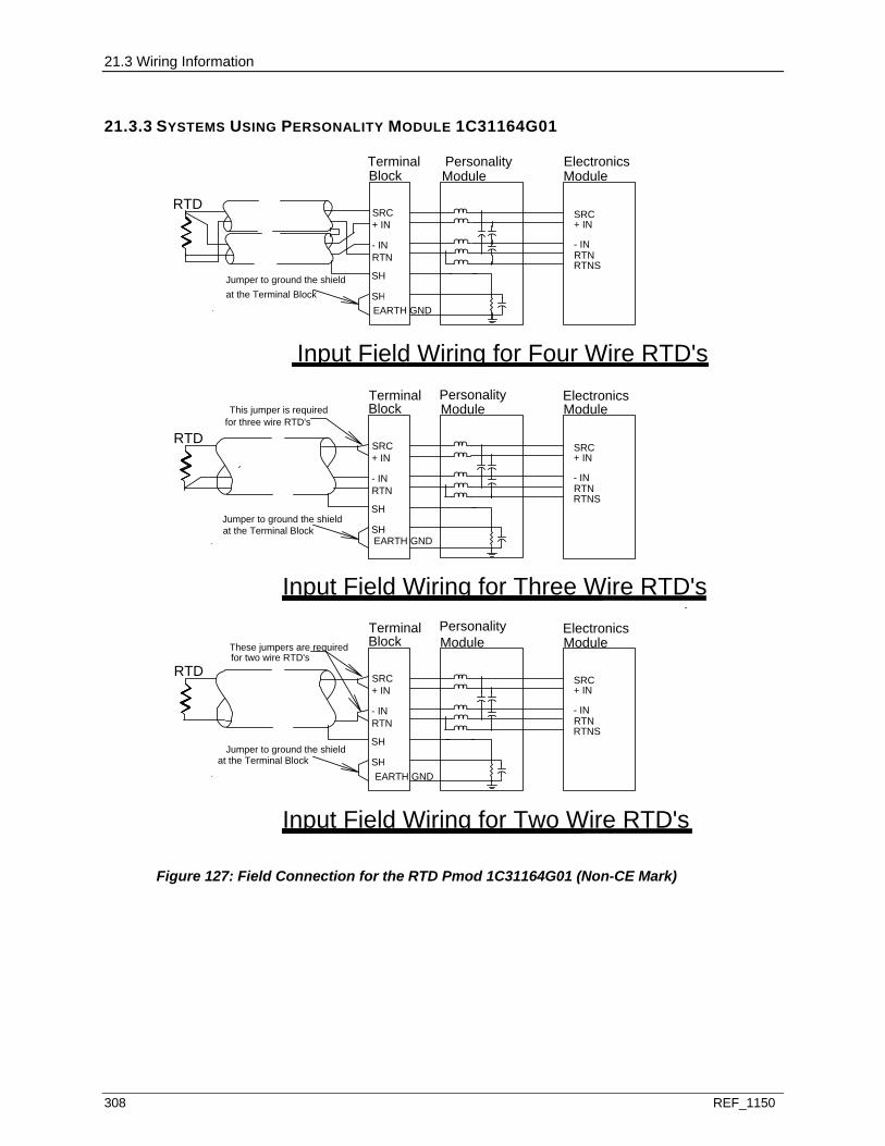
21.3 Wiring Information
308 REF_1150
21.3.3 SYSTEMS USING PERSONALITY MODULE 1C31164G01
Jumper to ground the shieldat the Terminal Block
These jumpers are requiredfor two wire RTD's
Jumper to ground the shieldat the Terminal Block
RTD
RTN
EARTH GNDSHG
SH
- IN
Block
SRC+ IN
Terminal
EARTH GNDSHG
SH
This jumper is requiredfor three wire RTD's
Jumper to ground the shieldat the Terminal Block
RTD
RTD
SHG
TerminalBlock
SRC+ IN
RTN- IN
EARTH GND
SRC+ IN
SH
RTN- IN
TerminalBlock
RTNS
ElectronicsModule
RTNRTNS
SRC
- IN
PersonalityModule
+ IN
ElectronicsModule
ElectronicsModule
SRC
RTN
SRC
RTNRTNS
PersonalityModule
+ IN
- IN
PersonalityModule
+ IN
- IN
Input Field Wiring for Four Wire RTD's
Input Field Wiring for Three Wire RTD's
Input Field Wiring for Two Wire RTD's
Figure 127: Field Connection for the RTD Pmod 1C31164G01 (Non-CE Mark)

21.3 Wiring Information
REF_1150 309
21.3.4 NON-CE MARK SYSTEMS USING PERSONALITY MODULE 1C31164G02
Input Field Wiring for Four Wire RTD's
Input Field Wiring for Three Wire RTD's
Input Field Wiring for Two Wire RTD's
JUMPER TO GROUND THE SHIELD
These jumpers are requiredfor two wire RTD's
JUMPER TO GROUND THE SHIELD
AT THE TERMINAL BLOCK
AT THE TERMINAL BLOCK
RTD
SH
RTN- IN
SRC+ IN
BlockTerminalTerminal
SH
JUMPER TO GROUND THE SHIELD
This jumper is requiredfor three wire RTD's
AT THE TERMINAL BLOCK
RTD
RTD
SH
Terminal
SRC+ IN
RTN- IN
Block
SRC+ IN
RTN- IN
BlockTerminalTerminal
RTNS
CH SHIELD
SRC
RTNRTNS
ElectronicsModule
CH GND
CH SHIELD
- IN
PersonalityModule
+ IN
SRC
RTNRTNS
ElectronicsModule
CH GND
CH SHIELD
SRC
RTN
ElectronicsModule
CH GND
PersonalityModule
+ IN
- IN
PersonalityModule
+ IN
- IN
EARTHGND
EARTHGND
EARTHGND
Figure 128: Field Connection for the RTD Personality Module (Non-CE Mark)
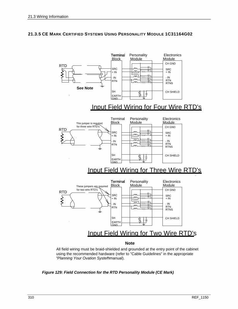
21.3 Wiring Information
310 REF_1150
21.3.5 CE MARK CERTIFIED SYSTEMS USING PERSONALITY MODULE 1C31164G02
All field wiring must be braid-shielded and grounded at the entry point of the cabinetusing the recommended hardware (refer to "Cable Guidelines" in the appropriate
Input Field Wiring for Two Wire RTD's
Input Field Wiring for Four Wire RTD's
Input Field Wiring for Three Wire RTD's
These jumpers are requiredfor two wire RTD's
RTD
SHEARTHGND
RTN- IN
SRC+ IN
BlockTerminalTerminal
SHEARTHGND
This jumper is requiredfor three wire RTD's
See Note 1
RTD
RTD
SH
Terminal
SRC+ IN
RTN- IN
Block
EARTHGND
SRC+ IN
RTN- IN
BlockTerminalTerminal
RTNS
CH SHIELD
SRC
RTNRTNS
ElectronicsModule
CH GND
CH SHIELD
- IN
PersonalityModule
+ IN
SRC
RTNRTNS
ElectronicsModule
CH GND
CH SHIELD
SRC
RTN
ElectronicsModule
CH GND
PersonalityModule
+ IN
- IN
PersonalityModule
+ IN
- IN
Note
"Planning Your Ovation System" manual).
See Note
Figure 129: Field Connection for the RTD Personality Module (CE Mark)

21.4 Address Location Information
REF_1150 311
21.4 ADDRESS LOCATION INFORMATION
21.4.1 CONFIGURATION AND STATUS REGISTER
Word address 13 (D in Hex) is used to configure the module and provide status information to the Controller.
Word address 13 (D in Hex) low byte is used for module configuration.
Word address 13 (D in Hex) high byte is used to define the scale for Channel 2.
The status register can be read by using the Point Information window at an Operator Station (see the Bit Pattern field on the Hardware tab). (See Ovation Operator Station User Guide.)
RTD Configuration/Status Register (Address 13 or D in Hex)
BI T DAT A DE S C R I P T I O N - CO N FI G U R AT I O N REGI S TE R (WRI TE)
DAT A DE S C R I P T I O N - ST ATUS REGI S TER (RE AD)
0 Configure Module Module Configured
(1 = configured; 0 = un-considered)
1 Force error Internal or forced error
(1 = forced error; 0 = no forced error)
2 Not used Point Fault bit (set when any point specific fault exists)
3 Not used Card trouble bit (set during card failure)
4 Not used Warming bit (set during power up or configuration)
5 50/60 Hz select (0 = 60Hz, 1 = 50Hz) 50/60 Hz select readback (0 = 60Hz, 1 = 50Hz)
6 Enable line frequency tracking. Status of the line frequency tracking enable signal.
7 Diagnostic bit (do not use).
When set in the “Diagnostics” mode, Bits 0 to 6 of the configuration register represent a word address of the Micro Controller’s internal memory.
Sync Fault (set if SYNC is missing or the reasonability test failed while the line frequency tracking is enabled)
8 - 15 Channel #2 scale configuration Channel #2 scale configuration read back
Note: Line frequency tracking is presently NOT supported by the Ovation I/O system.
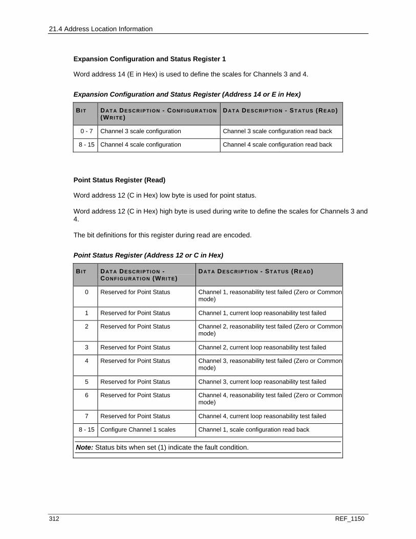
21.4 Address Location Information
312 REF_1150
Expansion Configuration and Status Register 1
Word address 14 (E in Hex) is used to define the scales for Channels 3 and 4.
Expansion Configuration and Status Register (Address 14 or E in Hex)
BI T DAT A DE S C R I P T I O N - CO NF I G U R AT I O N (WRI TE)
DAT A DE S C R I P T I O N - ST ATUS (RE AD)
0 - 7 Channel 3 scale configuration Channel 3 scale configuration read back
8 - 15 Channel 4 scale configuration Channel 4 scale configuration read back
Point Status Register (Read)
Word address 12 (C in Hex) low byte is used for point status.
Word address 12 (C in Hex) high byte is used during write to define the scales for Channels 3 and 4.
The bit definitions for this register during read are encoded.
Point Status Register (Address 12 or C in Hex)
BI T DAT A DE S C R I P T I O N - CO N FI G U R AT I O N (WRI T E)
DAT A DE S C R I P T I O N - ST ATUS (RE AD)
0 Reserved for Point Status Channel 1, reasonability test failed (Zero or Common mode)
1 Reserved for Point Status Channel 1, current loop reasonability test failed
2 Reserved for Point Status Channel 2, reasonability test failed (Zero or Common mode)
3 Reserved for Point Status Channel 2, current loop reasonability test failed
4 Reserved for Point Status Channel 3, reasonability test failed (Zero or Common mode)
5 Reserved for Point Status Channel 3, current loop reasonability test failed
6 Reserved for Point Status Channel 4, reasonability test failed (Zero or Common mode)
7 Reserved for Point Status Channel 4, current loop reasonability test failed
8 - 15 Configure Channel 1 scales Channel 1, scale configuration read back
Note: Status bits when set (1) indicate the fault condition.
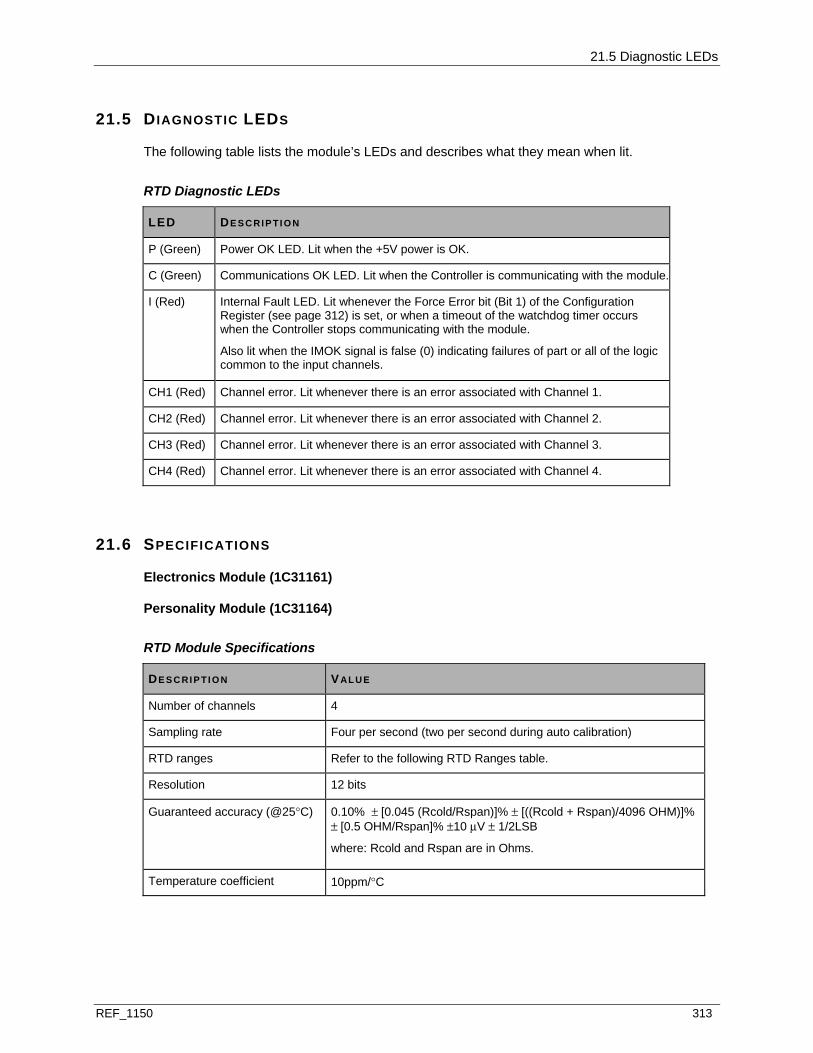
21.5 Diagnostic LEDs
REF_1150 313
21.5 DIAGNOSTIC LEDS
The following table lists the module’s LEDs and describes what they mean when lit.
RTD Diagnostic LEDs
LED DE S C RI P TI O N
P (Green) Power OK LED. Lit when the +5V power is OK.
C (Green) Communications OK LED. Lit when the Controller is communicating with the module.
I (Red) Internal Fault LED. Lit whenever the Force Error bit (Bit 1) of the Configuration Register (see page 312) is set, or when a timeout of the watchdog timer occurs when the Controller stops communicating with the module.
Also lit when the IMOK signal is false (0) indicating failures of part or all of the logic common to the input channels.
CH1 (Red) Channel error. Lit whenever there is an error associated with Channel 1.
CH2 (Red) Channel error. Lit whenever there is an error associated with Channel 2.
CH3 (Red) Channel error. Lit whenever there is an error associated with Channel 3.
CH4 (Red) Channel error. Lit whenever there is an error associated with Channel 4.
21.6 SPECIFICATIONS
Electronics Module (1C31161)
Personality Module (1C31164)
RTD Module Specifications
DE S C RI P TI O N VAL UE
Number of channels 4
Sampling rate Four per second (two per second during auto calibration)
RTD ranges Refer to the following RTD Ranges table.
Resolution 12 bits
Guaranteed accuracy (@25°C) 0.10% ± [0.045 (Rcold/Rspan)]% ± [((Rcold + Rspan)/4096 OHM)]% ± [0.5 OHM/Rspan]% ±10 μV ± 1/2LSB
where: Rcold and Rspan are in Ohms.
Temperature coefficient 10ppm/°C
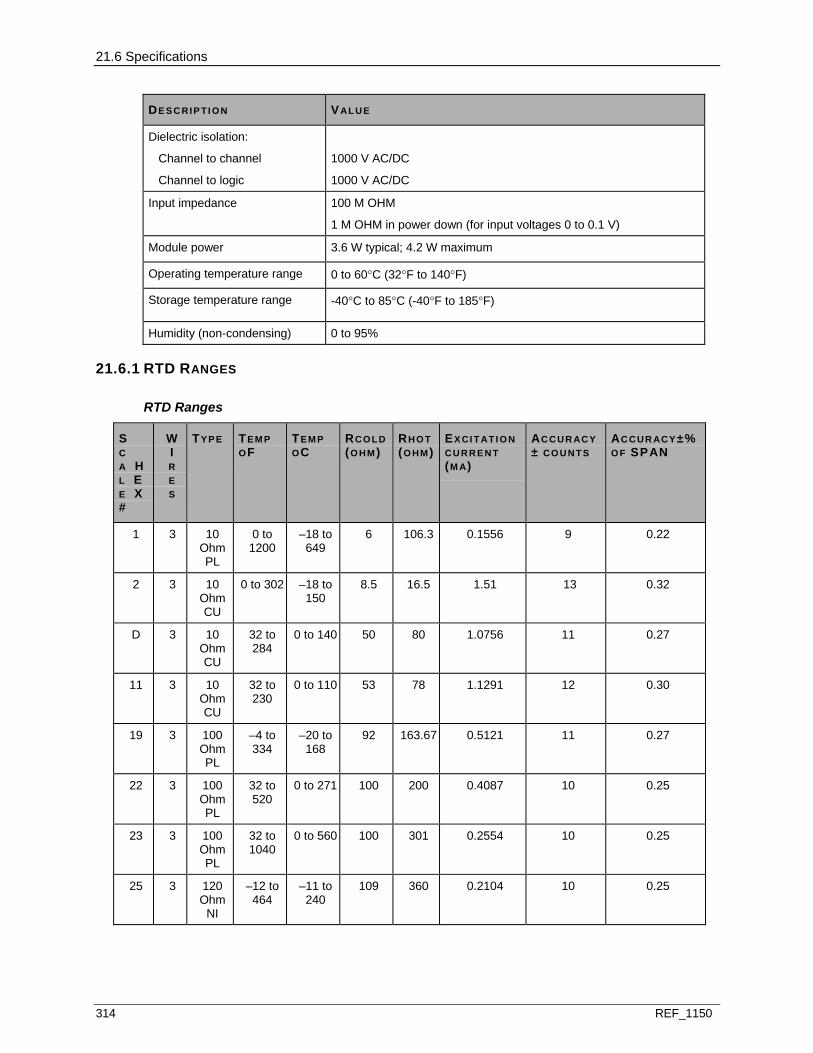
21.6 Specifications
314 REF_1150
DE S C RI P TI O N VAL UE
Dielectric isolation:
Channel to channel
Channel to logic
1000 V AC/DC
1000 V AC/DC
Input impedance 100 M OHM
1 M OHM in power down (for input voltages 0 to 0.1 V)
Module power 3.6 W typical; 4.2 W maximum
Operating temperature range 0 to 60°C (32°F to 140°F)
Storage temperature range -40°C to 85°C (-40°F to 185°F)
Humidity (non-condensing) 0 to 95%
21.6.1 RTD RANGES
RTD Ranges
S C A H L E E X #
W I R E S
TYP E TEM P OF
TEM P OC
RC O L D(O HM)
RH O T(O HM)
EX CI T AT I O NC U R R E N T (M A)
AC CUR ACY ± CO UNTS
AC CUR ACY±% O F SPAN
1 3 10 Ohm PL
0 to 1200
–18 to 649
6 106.3 0.1556 9 0.22
2 3 10 Ohm CU
0 to 302 –18 to 150
8.5 16.5 1.51 13 0.32
D 3 10 Ohm CU
32 to 284
0 to 140 50 80 1.0756 11 0.27
11 3 10 Ohm CU
32 to 230
0 to 110 53 78 1.1291 12 0.30
19 3 100 Ohm PL
–4 to 334
–20 to 168
92 163.67 0.5121 11 0.27
22 3 100 Ohm PL
32 to 520
0 to 271 100 200 0.4087 10 0.25
23 3 100 Ohm PL
32 to 1040
0 to 560 100 301 0.2554 10 0.25
25 3 120 Ohm
NI
–12 to 464
–11 to 240
109 360 0.2104 10 0.25

21.6 Specifications
REF_1150 315
S C A H L E E X #
W I R E S
TYP E TEM P OF
TEM P OC
RC O L D(O HM)
RH O T(O HM)
EX CI T AT I O NC U R R E N T (M A)
AC CUR ACY ± CO UNTS
AC CUR ACY±% O F SPAN
26 3 120 Ohm
NI
32 to 150
0 to 66 120 170 0.5240 13 0.32
28 3 120 Ohm
NI
32 to 252
0 to 122 120 225 0.3682 11 0.27
80 4 100 Ohm PL
32 to 544
0 to 290 100 208 0.3921 10 0.25
81 4 100 Ohm PL
356 to 446
180 to 230
168 186 0.5240 30 0.74
82 4 200 Ohm PL
32 to 698
0 to 370 200 473 0.1675 12 0.30
83 4 200 Ohm PL
514 to 648
268 to 342
402 452 0.2142 29 0.71
84 4 100 Ohm PL
32 to 124
0 to 51 100 120 0.7860 19 0.47
85 4 100 Ohm PL
32 to 217
0 to 103 100 140 0.6386 13 0.32
86 4 100 Ohm PL
32 to 412
0 to 211 100 180 0.4644 11 0.27
87 4 100 Ohm PL
32 to 714
0 to 379 100 240 0.3296 10 0.25
88 4 200 Ohm PL
511 to 662
266 to 350
200 230 0.4170 24 0.59

REF_1150 317
IN THIS SECTION
Description ......................................................................................................................317 Module Group Information ..............................................................................................318 Wiring Information ...........................................................................................................318 Address Location Information .........................................................................................322 Diagnostic LEDs..............................................................................................................325 Specifications ..................................................................................................................325
22.1 DESCRIPTION
The 8-channel RTD module is used to convert inputs from Resistance Temperature Detectors (RTDs) to digital data. The digitized data is transmitted to the Controller.
Note: I/O Module General Information (see page 15) contains environmental, installation, wiring, and fuse information for I/O modules.
CAUTION! The following applies to channels that are subsequently wired to an RTD after power is applied to the module.
If an RTD is wired into a live eight channel RTD module, one of the following two conditions must be met to insure reading of the RTD:
1. Module power must be cycled after the RTD is installed.
2. The particular point to which the RTD is installed must be configured or re-configured after the RTD is installed.
Please note that there are no considerations necessary if the RTD is installed prior to power being applied to the module. Further, once the conditions for proper operations are met, the RTD can be removed and subsequently re-installed at which time it will be read correctly without any further considerations.
S E C T I O N 2 2
RTD MODULE (8 CHANNEL)
22.2 Module Group Information
318 REF_1150
22.2 MODULE GROUP INFORMATION
22.2.1 ELECTRONICS MODULE (EMOD)
There is one Electronics module group for the 8-channel RTD Module:
5X00119G01 converts inputs for all ranges and is compatible only with Personality module 5X00121G01.
22.2.2 PERSONALITY MODULE (PMOD)
There is one Personality module group for the 8-channel RTD Module:
5X00121G01 converts inputs for all ranges and is compatible only with Electronics module 5X00119G01.
22.2.3 SUBSYSTEMS, 8-CHANNEL RTD MODULE
8-Channel RTD Module Subsystems
CH AN N E L S EL E CT RO NI C MO D U LE PE R S O N AL I T Y MODULE
8 5X00119G01 5X00121G01
22.3 WIRING INFORMATION
22.3.1 RTD (8 CHANNEL) SYSTEMS (USING PMOD 5X00121G01) TERMINAL BLOCK WIRING INFORMATION
Each Personality module has a simplified wiring diagram label on its side, which appears above the terminal block. This diagram indicates how the wiring from the field is to be connected to the terminal block in the base unit. The following table lists and defines the abbreviations used in this diagram.
Abbreviations Used in the Diagram
Abbreviation Definition
+IN, -IN Positive and negative sense input connection.
Earth ground terminal. Used for landing shields when the shield is to be grounded at the module.
PS+, PS- Auxiliary power supply terminals.
RTN Return for current source connection.
SH Shield connector. Used for landing shields when the shield is to be grounded at the RTD.
SRC Current source connection.
Note: PS+ and PS- are not used by this module.

22.3 Wiring Information
REF_1150 319
22.3.2 MODULE AND FIELD CONNECTION WIRING
The Ovation 8-Channel RTD module consists of two modules, an electronics module containing a logic printed circuit board (LIA) and a printed circuit board (FTD). The electronics module is used in conjunction with a personality module, which contains a single printed circuit board (PTD). The block diagram for the 8-channel RTD module is shown below.


REF_1150 321
Module Block Diagram and Field Connection Wiring Diagram
A/D
con
vert
er,
pow
er c
lock
, &
dat
a
Logi
c Po
wer
Su
pply
24v main (A)
24v main (B)
main return
I/O bus
6 7 8 9 10 11 12 13 14 15 16 17 18
AB
C
1 2 4 53
P7+
EGN
D (A
1)
24V AUXAUX
RETURNEARTH
ELEC
TRO
NIC
S M
OD
ULE
–+
A/D
Po
wer
su
pply
&
Dat
a I/F
I/O B
ase
Con
nect
or to
Oth
er I/
O B
ases
and
/or C
ontr
olle
r
PER
SON
ALI
TY
MO
DU
LE
A/D
C
onve
rter
I/O
Inte
rfac
e
Proc
esso
r
CH
AN
NEL
1 (F
our w
ire fi
eld
inte
rfac
e, lo
cal s
hiel
d gr
ound
ing)
–+
AB
C
I/O B
ASE
TE
RM
INA
TIO
NS
8 C
HA
NN
EL R
TD
INPU
T M
OD
ULE
FU
NC
TIO
NA
L D
IAG
RA
M
I/O B
ase
Con
nect
or to
Oth
er I/
O B
ases
A/D
Po
wer
su
pply
&
Dat
a I/F
ISOLATION BARRIER
CH
AN
NE
LS 2
- 7
FIEL
D
CO
NN
ECTI
ON
S
SH SH SH SH SH SH SH SH
SRC SRC SRC SRC SRC SRC SRC SRC+IN +IN +IN +IN +IN +IN +IN +IN
-IN -IN -IN -IN -IN -IN -IN -INRTN RTN RTN RTN RTN RTN RTN RTN
SHIE
LD (A
2)
+IN
(B2)
-IN (C
1)
SRC
(B1)
RTN
(C2)
Cur
rent
So
urce
Low
Pa
ss
Filte
r
inpu
t #1 Inpu
t #2
Mux
Vref
A/D
con
vert
er,
pow
er c
lock
, &
dat
a
A/D
C
onve
rter
Cur
rent
So
urce
Low
Pa
ss
Filte
r
inpu
t #1 Inpu
t #2
Mux
Vref
EGN
D (A
15)
SHIE
LD (A
16)
+IN
(B16
)
-IN (C
15)
SRC
(B15
)
RTN
(C16
)
CH
AN
NEL
8 (T
hree
wire
fiel
d in
terf
ace,
rem
ote
shie
ld g
roun
ding
)
RTN
SRC
4 W
IRE
RTD
Not
e: th
is e
xam
ple
show
s th
e sh
ield
gr
ound
ed a
t the
mod
ule.
It m
ay b
e op
tiona
lly g
roun
ded
at th
e R
TD.
3 W
IRE
RTD
RTN
Not
e: th
is e
xam
ple
show
s th
e sh
ield
gr
ound
ed a
t the
RTD
. It
may
be
optio
nally
gro
unde
d at
the
mod
ule.
PS+
PS+
PS-
Jum
per r
equi
red
for 3
-wire
RTD
s
Figure 130: 8-Channel RTD Block Diagram and Field Connection Wiring Diagram

22.4 Address Location Information
322 REF_1150
22.4 ADDRESS LOCATION INFORMATION
22.4.1 CONFIGURATION AND STATUS REGISTER
Word address 13 (D in Hex) is used to configure the module and provide status information to the Controller. The status register can be read by using the Point Information window at an Operator Station (Bit Pattern Field on the Hardware Tab). (See the Ovation Operator Station User Guide.)
8-Channel RTD Configuration/Status Register (Address 13 or D in Hex)
Bit Data Description - Configuration Register (Write)
Data Description - Status Register (Read)
0 Configure Module Module Configured
(1 = configured; 0 = unconfigured)
1 Force error Internal or forced error
(1 = forced error; 0 = no forced error)
2 50/60 Hz select (0 = 60Hz, 1 = 50Hz) 50/60 Hz System (1 = 50Hz) (read back)
3 SELF_CAL (Initiates Self Calibration) Warming bit (set during power up or configuration)
4 0 0
5 0 0
6 0 Module Not Calibrated
7 0 0
8 Channel 1 _ 3/4 Wire Channel 1 _ 3/4 Wire - Configuration (read back)
9 Channel 2 _ 3/4 Wire Channel 2 _ 3/4 Wire - Configuration (read back)
10 Channel 3 _ 3/4 Wire Channel 3 _ 3/4 Wire - Configuration (read back)
11 Channel 4 _ 3/4 Wire Channel 4 _ 3/4 Wire - Configuration (read back)
12 Channel 5 _ 3/4 Wire Channel 5 _ 3/4 Wire - Configuration (read back)
13 Channel 6 _ 3/4 Wire Channel 6 _ 3/4 Wire - Configuration (read back)
14 Channel 7 _ 3/4 Wire Channel 7 _ 3/4 Wire - Configuration (read back)
15 Channel 8 _ 3/4 Wire Channel 8 _ 3/4 Wire - Configuration (read back)
Definitions for the Configuration/Module Status Register bits:
Bit 0: This bit configures the module (write) or indicates the configuration state of the module (read). A “1” indicates that the module is configured. Note that until the module is configured, reading from addresses 0 through 11 (B in Hex) will produce an attention status.
Bit 1: This bit (write “1”) forces the module into the error state, resulting in the error LED being lit. The read of bit “1” indicates that there is an internal module error, or the controller has forced the module into the error state. The state of this bit is always reflected by the module’s Internal Error LED. Whenever this bit is set, an attention status is returned to the controller when address 0 through 11 (B in Hex) are read.
22.4 Address Location Information
REF_1150 323
Bit 2: The status of this bit (read) indicates the conversion rate of the module, write to this bit configures the conversion rate of A/D converters as shown below.
CO N VE R SI O N RAT E (1 /SE C. ) BI T 2
60 (for 60Hz systems) 0
50 (for 50Hz systems) 1
Bit3: Write: This bit is used to initiate self-calibration. Read: This bit indicates that the module is in the “Warming” state. This state exists after power up and terminates after 8.16 seconds. The module will be in the error condition during the warm up period.
Bits 4 - 5: These bits are not used and read as “0” under normal operation.
Bit 6: This bit (read) is the result of a checksum test of the EEPROM. A failure of this test can indicate a bad EEPROM, but it typically indicates that the module has not been calibrated. A “0” indicates that there is no error condition. If an error is present, the internal error LED is lit and attention status will be returned for all address offsets 0-11 (0x0 - 0xB). The “1” state of this bit indicates an unrecoverable error condition in the field.
Bit 7: This bit is not used and read as “0” under normal operation.
Bits 8 - 15: These bits are used to configure channels 1 - 8 respectively for 3 or 4 wire operation. A “0” indicates 3 wire and a “1” indicates 4 wire operation, see the tables below).
22.4.2 CHANNEL SCALE CONFIGURATION REGISTERS
Word addresses 12 and 14 (described in the following two tables) are used to configure the appropriate scales for Channels 1 - 8 (refer to Column 1 in the table in Specifications (see page 325)).
Data Format for the Channel Scale Configuration Register (Address 12 or C in Hex)
BI T DAT A DE S C R I P T I O N - CO N FI G U R AT I O N (WRI T E)
DAT A DE S C R I P T I O N - ST ATUS (RE AD)
0 Configure Channel #1scale - Bit 0 Channel #1 scale configuration (read back) - Bit 0
1 Configure Channel #1scale - Bit 1 Channel #1 scale configuration (read back) - Bit 1
2 Configure Channel #1scale - Bit 2 Channel #1 scale configuration (read back) - Bit 2
3 Configure Channel #1scale - Bit 3 Channel #1 scale configuration (read back) - Bit 3
4 Configure Channel #2 scale - Bit 0 Channel #2 scale configuration (read back) - Bit 0
5 Configure Channel #2 scale - Bit 1 Channel #2 scale configuration (read back) - Bit 1
6 Configure Channel #2 scale - Bit 2 Channel #2 scale configuration (read back) - Bit 2
7 Configure Channel #2 scale - Bit 3 Channel #2 scale configuration (read back) - Bit 3
8 Configure Channel #3 scale - Bit 0 Channel #3 scale configuration (read back) - Bit 0
9 Configure Channel #3 scale - Bit 1 Channel #3 scale configuration (read back) - Bit 1
10 Configure Channel #3 scale - Bit 2 Channel #3 scale configuration (read back) - Bit 2
11 Configure Channel #3 scale - Bit 3 Channel #3 scale configuration (read back) - Bit 3
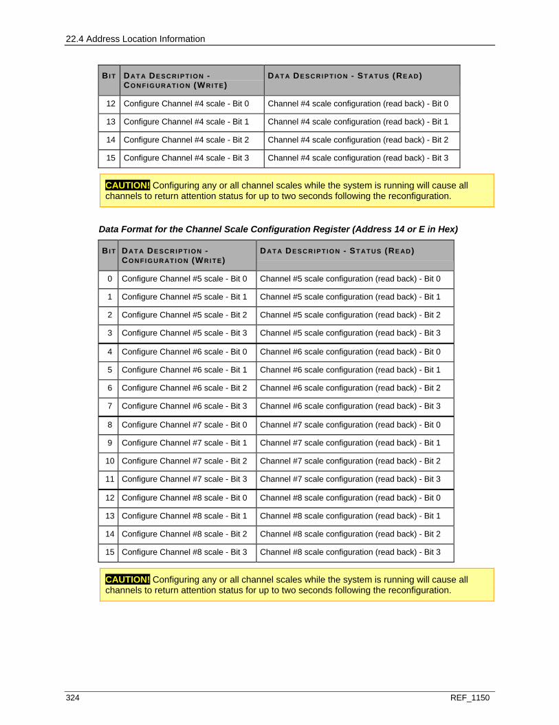
22.4 Address Location Information
324 REF_1150
BI T DAT A DE S C R I P T I O N - CO N FI G U R AT I O N (WRI T E)
DAT A DE S C R I P T I O N - ST ATUS (RE AD)
12 Configure Channel #4 scale - Bit 0 Channel #4 scale configuration (read back) - Bit 0
13 Configure Channel #4 scale - Bit 1 Channel #4 scale configuration (read back) - Bit 1
14 Configure Channel #4 scale - Bit 2 Channel #4 scale configuration (read back) - Bit 2
15 Configure Channel #4 scale - Bit 3 Channel #4 scale configuration (read back) - Bit 3
CAUTION! Configuring any or all channel scales while the system is running will cause all channels to return attention status for up to two seconds following the reconfiguration.
Data Format for the Channel Scale Configuration Register (Address 14 or E in Hex)
BI T DAT A DE S C R I P T I O N - CO N FI G U R AT I O N (WRI T E)
DAT A DE S C R I P T I O N - ST ATUS (RE AD)
0 Configure Channel #5 scale - Bit 0 Channel #5 scale configuration (read back) - Bit 0
1 Configure Channel #5 scale - Bit 1 Channel #5 scale configuration (read back) - Bit 1
2 Configure Channel #5 scale - Bit 2 Channel #5 scale configuration (read back) - Bit 2
3 Configure Channel #5 scale - Bit 3 Channel #5 scale configuration (read back) - Bit 3
4 Configure Channel #6 scale - Bit 0 Channel #6 scale configuration (read back) - Bit 0
5 Configure Channel #6 scale - Bit 1 Channel #6 scale configuration (read back) - Bit 1
6 Configure Channel #6 scale - Bit 2 Channel #6 scale configuration (read back) - Bit 2
7 Configure Channel #6 scale - Bit 3 Channel #6 scale configuration (read back) - Bit 3
8 Configure Channel #7 scale - Bit 0 Channel #7 scale configuration (read back) - Bit 0
9 Configure Channel #7 scale - Bit 1 Channel #7 scale configuration (read back) - Bit 1
10 Configure Channel #7 scale - Bit 2 Channel #7 scale configuration (read back) - Bit 2
11 Configure Channel #7 scale - Bit 3 Channel #7 scale configuration (read back) - Bit 3
12 Configure Channel #8 scale - Bit 0 Channel #8 scale configuration (read back) - Bit 0
13 Configure Channel #8 scale - Bit 1 Channel #8 scale configuration (read back) - Bit 1
14 Configure Channel #8 scale - Bit 2 Channel #8 scale configuration (read back) - Bit 2
15 Configure Channel #8 scale - Bit 3 Channel #8 scale configuration (read back) - Bit 3
CAUTION! Configuring any or all channel scales while the system is running will cause all channels to return attention status for up to two seconds following the reconfiguration.
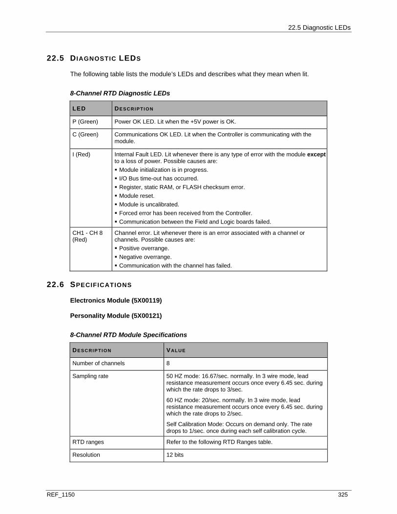
22.5 Diagnostic LEDs
REF_1150 325
22.5 DIAGNOSTIC LEDS
The following table lists the module’s LEDs and describes what they mean when lit.
8-Channel RTD Diagnostic LEDs
LED DE S C RI P TI O N
P (Green) Power OK LED. Lit when the +5V power is OK.
C (Green) Communications OK LED. Lit when the Controller is communicating with the module.
I (Red) Internal Fault LED. Lit whenever there is any type of error with the module exceptto a loss of power. Possible causes are: Module initialization is in progress. I/O Bus time-out has occurred. Register, static RAM, or FLASH checksum error. Module reset. Module is uncalibrated. Forced error has been received from the Controller. Communication between the Field and Logic boards failed.
CH1 - CH 8 (Red)
Channel error. Lit whenever there is an error associated with a channel or channels. Possible causes are: Positive overrange. Negative overrange. Communication with the channel has failed.
22.6 SPECIFICATIONS
Electronics Module (5X00119)
Personality Module (5X00121)
8-Channel RTD Module Specifications
DE S C RI P TI O N VALUE
Number of channels 8
Sampling rate 50 HZ mode: 16.67/sec. normally. In 3 wire mode, lead resistance measurement occurs once every 6.45 sec. during which the rate drops to 3/sec.
60 HZ mode: 20/sec. normally. In 3 wire mode, lead resistance measurement occurs once every 6.45 sec. during which the rate drops to 2/sec.
Self Calibration Mode: Occurs on demand only. The rate drops to 1/sec. once during each self calibration cycle.
RTD ranges Refer to the following RTD Ranges table.
Resolution 12 bits
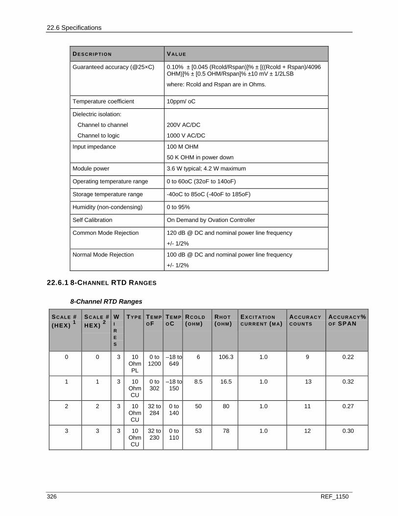
22.6 Specifications
326 REF_1150
DE S C RI P TI O N VALUE
Guaranteed accuracy (@25×C) 0.10% ± [0.045 (Rcold/Rspan)]% ± [((Rcold + Rspan)/4096 OHM)]% ± [0.5 OHM/Rspan]% ±10 mV ± 1/2LSB
where: Rcold and Rspan are in Ohms.
Temperature coefficient 10ppm/ oC
Dielectric isolation:
Channel to channel
Channel to logic
200V AC/DC
1000 V AC/DC
Input impedance 100 M OHM
50 K OHM in power down
Module power 3.6 W typical; 4.2 W maximum
Operating temperature range 0 to 60oC (32oF to 140oF)
Storage temperature range -40oC to 85oC (-40oF to 185oF)
Humidity (non-condensing) 0 to 95%
Self Calibration On Demand by Ovation Controller
Common Mode Rejection 120 dB @ DC and nominal power line frequency
+/- 1/2%
Normal Mode Rejection 100 dB @ DC and nominal power line frequency
+/- 1/2%
22.6.1 8-CHANNEL RTD RANGES
8-Channel RTD Ranges
SC AL E #
(HEX) 1
SC AL E #
HEX) 2
WI R E S
TYP E TEM POF
TEM POC
RC O L D (O HM)
RH O T (O HM)
EX CI T AT I O N C U R R E N T (M A)
AC CUR ACYC O U N T S
AC CUR ACY%O F SPAN
0 0 3 10 Ohm PL
0 to 1200
–18 to 649
6 106.3 1.0 9 0.22
1 1 3 10 Ohm CU
0 to 302
–18 to 150
8.5 16.5 1.0 13 0.32
2 2 3 10 Ohm CU
32 to 284
0 to 140
50 80 1.0 11 0.27
3 3 3 10 Ohm CU
32 to 230
0 to 110
53 78 1.0 12 0.30
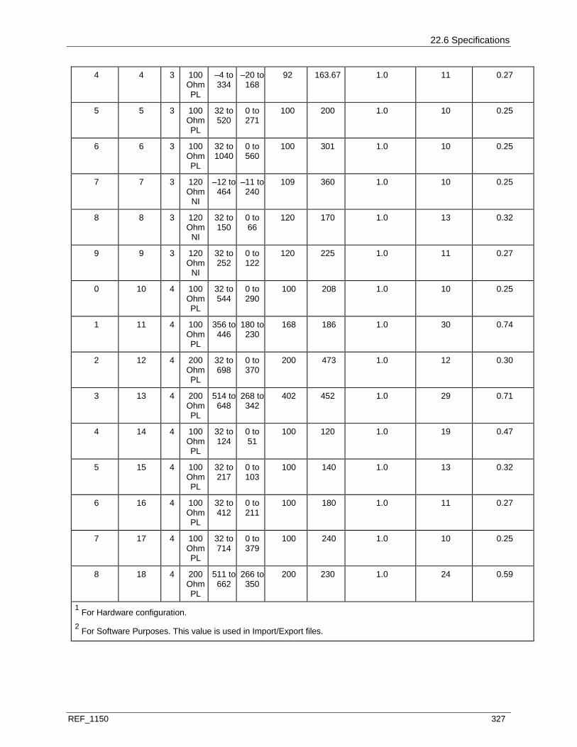
22.6 Specifications
REF_1150 327
4 4 3 100 Ohm PL
–4 to 334
–20 to 168
92 163.67 1.0 11 0.27
5 5 3 100 Ohm PL
32 to 520
0 to 271
100 200 1.0 10 0.25
6 6 3 100 Ohm PL
32 to 1040
0 to 560
100 301 1.0 10 0.25
7 7 3 120 Ohm
NI
–12 to 464
–11 to 240
109 360 1.0 10 0.25
8 8 3 120 Ohm
NI
32 to 150
0 to 66
120 170 1.0 13 0.32
9 9 3 120 Ohm
NI
32 to 252
0 to 122
120 225 1.0 11 0.27
0 10 4 100 Ohm PL
32 to 544
0 to 290
100 208 1.0 10 0.25
1 11 4 100 Ohm PL
356 to 446
180 to 230
168 186 1.0 30 0.74
2 12 4 200 Ohm PL
32 to 698
0 to 370
200 473 1.0 12 0.30
3 13 4 200 Ohm PL
514 to 648
268 to 342
402 452 1.0 29 0.71
4 14 4 100 Ohm PL
32 to 124
0 to 51
100 120 1.0 19 0.47
5 15 4 100 Ohm PL
32 to 217
0 to 103
100 140 1.0 13 0.32
6 16 4 100 Ohm PL
32 to 412
0 to 211
100 180 1.0 11 0.27
7 17 4 100 Ohm PL
32 to 714
0 to 379
100 240 1.0 10 0.25
8 18 4 200 Ohm PL
511 to 662
266 to 350
200 230 1.0 24 0.59
1 For Hardware configuration. 2 For Software Purposes. This value is used in Import/Export files.

REF_1150 329
IN THIS SECTION
Description ......................................................................................................................330 Module Group Information ..............................................................................................331 Module Specific Information............................................................................................331 Wiring Information, Sequence of Events Modules..........................................................332 Address Location Information .........................................................................................347 Diagnostic LEDs..............................................................................................................348 Specifications ..................................................................................................................348
S E C T I O N 2 3
SEQUENCE OF EVENTS MODULE

23.1 Description
330 REF_1150
23.1 DESCRIPTION
The Sequence of Events (SOE) module provides 16 digital channels to monitor the open or closed state of digital inputs or contacts in the field. The module provides a filter to reject changes of state less than four milliseconds. The Sequence of Events module can also perform event tagging and chatter control for each input channel.
The Ovation Controller writes a channel event tagging mask to the Electronics module to enable event tagging for specific input channels. It has a chatter control flag for each channel to indicate that an input channel has changed state too many times in a period of time or is changing state at too fast a rate. It also has a channel ID to indicate which channel changed state.
Each channel is checked every 125 microseconds. If the channel event tagging mask bit is zero, that channel is not checked. Time synchronization is accomplished by the Ovation Controller writing a time reference simultaneously to all Sequence of Events modules with a 1 millisecond resolution.
Note: I/O Module General Information (see page 15) contains environmental, installation, wiring, and fuse information for I/O modules. All SOE modules in a Controller MUST be connected to the IOIC card that is configured as the Time Keeper.
A control bit written by the Ovation Controller provides two options for handling input chatter:
The first option will set the chatter control flag if the rate of change for an input is greater than 1 per 100 milliseconds.
The second option sets the chatter control flag if 4 or more state changes occur on an input between reads of the event buffer.
There are two 32 event buffers. This allows the event tagging and chatter control function to be writing into one event buffer while the Ovation Controller is reading the other event buffer. The Ovation Controller only reads each module a small portion of the loop time. This allows both event buffers to be available the rest of the loop time.
Each event buffer contains 64 words with up to 32 Channel-IDs and 32 Event-Times. The event buffers are memories. The memory control circuit controls which event buffer to write into and which event buffer to read from. Before reading the event buffer, the buffer status register must be read to determine the number of words to read.
The Sequence of Events Module is applicable for CE Mark Certified Systems.
CAUTION! (For CE Mark certified systems) Any base unit that contains a 125VDC Sequence of Events Electronics module (1C31157G02) with differential Digital Input Personality module (1C31110G02) and interfaces to hazardous voltage (>60 VDC) must include a hazardous voltage warning label (1B30025H01) on that base unit.
Any base unit that contains a 125VDC Sequence of Events Electronics module (1C31157G02) with single-ended Digital Input Personality module (1C31110G01) and interfaces to hazardous voltage (>60 VDC) must include a hazardous voltage warning label (1B30025H01) on ALL base units on the branch.
This label must be placed in a visible location on the base unit, preferably above the spare fuse location. The project drawings must indicate this.
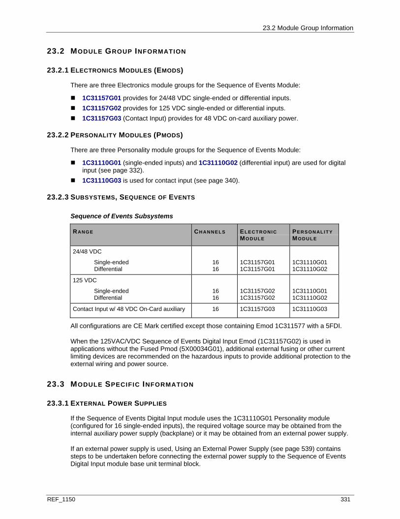
23.2 Module Group Information
REF_1150 331
23.2 MODULE GROUP INFORMATION
23.2.1 ELECTRONICS MODULES (EMODS)
There are three Electronics module groups for the Sequence of Events Module:
1C31157G01 provides for 24/48 VDC single-ended or differential inputs. 1C31157G02 provides for 125 VDC single-ended or differential inputs. 1C31157G03 (Contact Input) provides for 48 VDC on-card auxiliary power.
23.2.2 PERSONALITY MODULES (PMODS)
There are three Personality module groups for the Sequence of Events Module:
1C31110G01 (single-ended inputs) and 1C31110G02 (differential input) are used for digital input (see page 332).
1C31110G03 is used for contact input (see page 340).
23.2.3 SUBSYSTEMS, SEQUENCE OF EVENTS
Sequence of Events Subsystems
RANG E CH AN N E L S EL E CT RO NI C MO D U LE
PE R S O N AL I T Y MO D U LE
24/48 VDC
Single-ended Differential
16 16
1C31157G01 1C31157G01
1C31110G01 1C31110G02
125 VDC
Single-ended Differential
16 16
1C31157G02 1C31157G02
1C31110G01 1C31110G02
Contact Input w/ 48 VDC On-Card auxiliary 16 1C31157G03 1C31110G03
All configurations are CE Mark certified except those containing Emod 1C311577 with a 5FDI.
When the 125VAC/VDC Sequence of Events Digital Input Emod (1C31157G02) is used in applications without the Fused Pmod (5X00034G01), additional external fusing or other current limiting devices are recommended on the hazardous inputs to provide additional protection to the external wiring and power source.
23.3 MODULE SPECIFIC INFORMATION
23.3.1 EXTERNAL POWER SUPPLIES
If the Sequence of Events Digital Input module uses the 1C31110G01 Personality module (configured for 16 single-ended inputs), the required voltage source may be obtained from the internal auxiliary power supply (backplane) or it may be obtained from an external power supply.
If an external power supply is used, Using an External Power Supply (see page 539) contains steps to be undertaken before connecting the external power supply to the Sequence of Events Digital Input module base unit terminal block.
23.4 Wiring Information, Sequence of Events Modules
332 REF_1150
23.4 WIRING INFORMATION, SEQUENCE OF EVENTS MODULES
The Sequence of Events modules can be divided into two types depending on their front end connections, Digital Input Field Interface or Contact Filed Interface. The digital Input field Interface modules can be broken down further into Single-Ended and Differential as well as low and high voltage.
The following wiring section topics will be split to show the wiring of the Sequence of Events Digital Input Field Interface modules, then the Sequence of Events Contact Filed Interface modules.
23.4.1 SEQUENCE OF EVENTS DIGITAL INPUT FIELD INTERFACE MODULES
Digital Input Field Interface
The Digital Input configuration contains 16 channels, where each channel has voltage level sensing circuitry used to detect whether an input is on or off. The Sequence of Events module has 16 isolated differential inputs to accommodate separate external auxiliary supplies, or 16 single-ended (common return) digital inputs with an on-card blown fuse detector to accommodate a common external auxiliary supply for all channels. The selection of the Personality module determines if the inputs are differential or single-ended. The input voltage level monitored by the module is determined by the particular card group in the module.
The field side circuitry for the single-ended configuration and the differential configuration is shown under Field Wiring Considerations for the Digital Input Configuration (see page 333). An input resistor provides the normal mode surge protection and limits the current during normal operation. An opto-isolator provides high dielectric isolation between the field side and the logic or I/O bus side. The Single-Ended Digital Input configuration has a circuit used to monitor the presence of the wetting supply. Two cases cause this monitor circuitry to report a blown fuse status and issue an attention status to the Ovation Controller:
Fuse is blown on the PDIA. Auxiliary supply level is lower than minimum On Input Voltage.
SEQUENCE OF EVENTS DIGITAL INPUT TERMINAL BLOCK WIRING INFORMATION
Each Personality module has a simplified wiring diagram label on its side, which appears above the terminal block. This diagram indicates how the wiring from the field is to be connected to the terminal block in the base unit. The diagrams for the Sequence of Events digital input Personality modules are illustrated below.
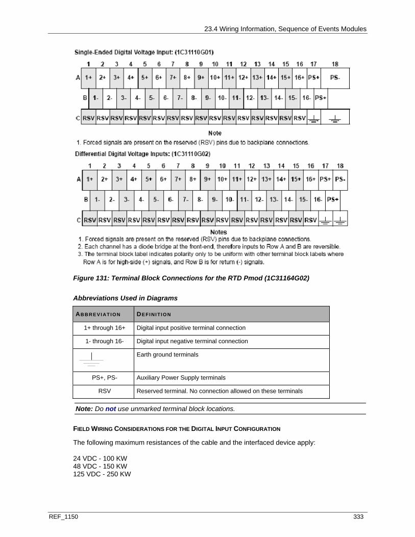
23.4 Wiring Information, Sequence of Events Modules
REF_1150 333
Figure 131: Terminal Block Connections for the RTD Pmod (1C31164G02)
Abbreviations Used in Diagrams
AB B R E V I AT I ON DE FI NI T I O N
1+ through 16+ Digital input positive terminal connection
1- through 16- Digital input negative terminal connection
Earth ground terminals
PS+, PS- Auxiliary Power Supply terminals
RSV Reserved terminal. No connection allowed on these terminals
Note: Do not use unmarked terminal block locations.
FIELD WIRING CONSIDERATIONS FOR THE DIGITAL INPUT CONFIGURATION
The following maximum resistances of the cable and the interfaced device apply:
24 VDC - 100 KW 48 VDC - 150 KW 125 VDC - 250 KW
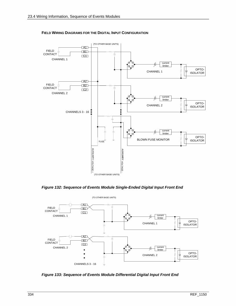
23.4 Wiring Information, Sequence of Events Modules
334 REF_1150
FIELD WIRING DIAGRAMS FOR THE DIGITAL INPUT CONFIGURATION
OPTO-ISOLATOR
A1B1C1
FIELDCONTACT
CHANNEL 1currentlimiter
OPTO-ISOLATOR
currentlimiter
A2B2C2
FIELDCONTACT
CHANNEL 2
CHANNELS 3 - 16
WE
TTING
VOLTA
GE
+
WETTIN
G VO
LTAG
E -
(TO OTHER BASE UNITS)
(TO OTHER BASE UNITS)
FUSE
OPTO-ISOLATOR
currentlimiter
CHANNEL 1
CHANNEL 2
BLOWN FUSE MONITORAU
XILIARY
AUXILIAR
Y
Figure 132: Sequence of Events Module Single-Ended Digital Input Front End
OPTO-ISOLATOR
A1B1C1
FIELDCONTACT
CHANNEL 1 currentlimiter
OPTO-ISOLATOR
currentlimiter
A2B2C2
FIELDCONTACT
CHANNEL 2
CHANNELS 3 - 16
(TO OTHER BASE UNITS)
CHANNEL 1
CHANNEL 2
DC
DC
Figure 133: Sequence of Events Module Differential Digital Input Front End
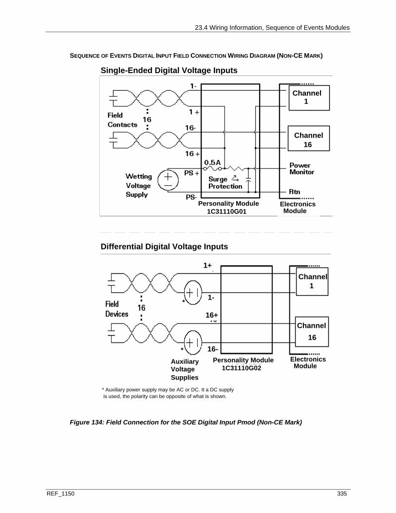
23.4 Wiring Information, Sequence of Events Modules
REF_1150 335
SEQUENCE OF EVENTS DIGITAL INPUT FIELD CONNECTION WIRING DIAGRAM (NON-CE MARK)
Single-Ended Digital Voltage Inputs
Differential Digital Voltage Inputs
1C31110G01 Personality Module
1C31110G02 Personality Module
ElectronicsModule
ElectronicsModuleAuxiliary
VoltageSupplies
Channel1
Channel
Channel
Channel
16
1
16
* Auxiliary power supply may be AC or DC. It a DC supply is used, the polarity can be opposite of what is shown.
1+
16+
1-
16-
*
*
Figure 134: Field Connection for the SOE Digital Input Pmod (Non-CE Mark)
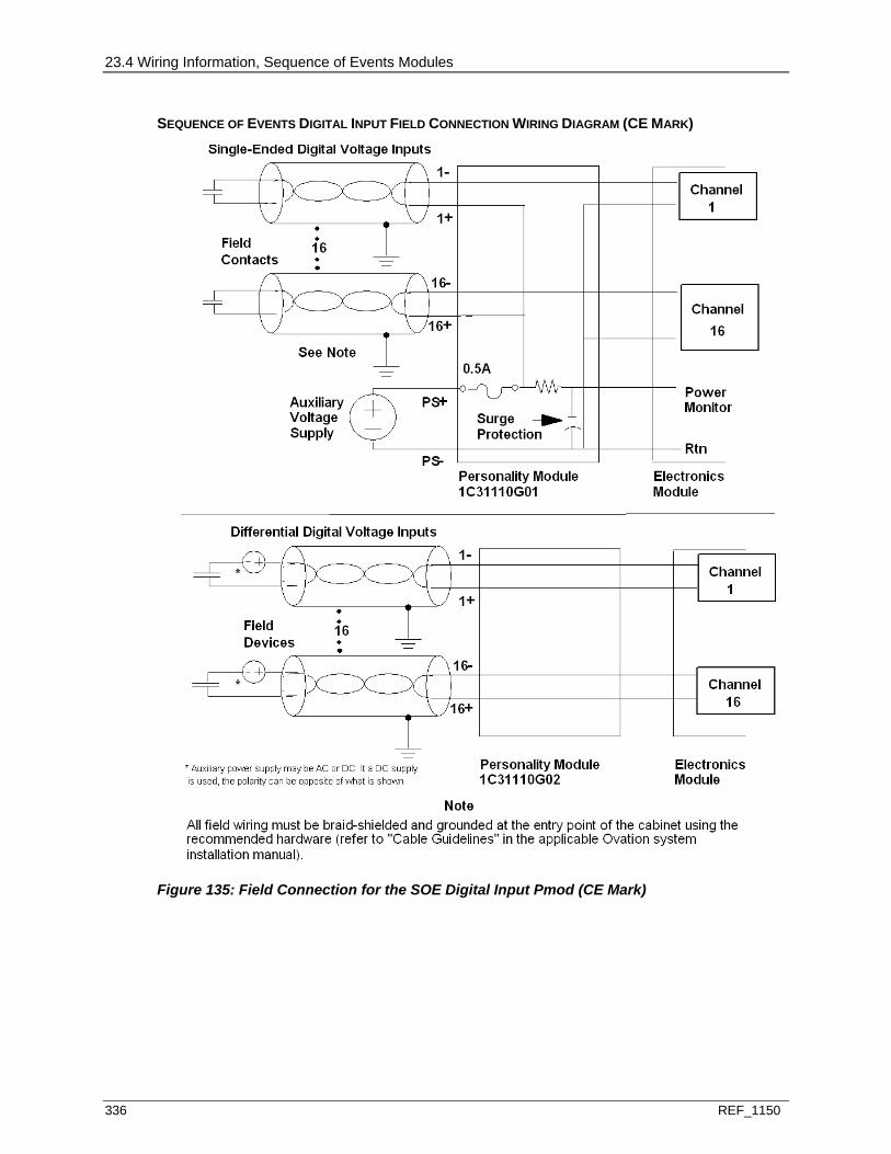
23.4 Wiring Information, Sequence of Events Modules
336 REF_1150
SEQUENCE OF EVENTS DIGITAL INPUT FIELD CONNECTION WIRING DIAGRAM (CE MARK)
Figure 135: Field Connection for the SOE Digital Input Pmod (CE Mark)
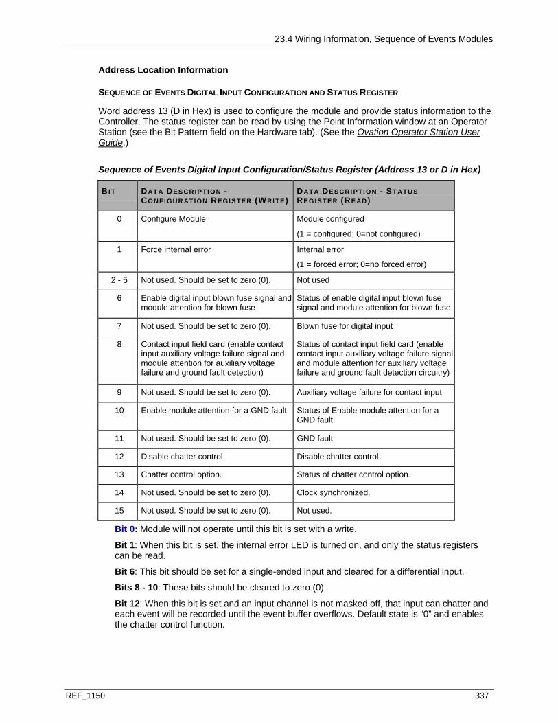
23.4 Wiring Information, Sequence of Events Modules
REF_1150 337
Address Location Information
SEQUENCE OF EVENTS DIGITAL INPUT CONFIGURATION AND STATUS REGISTER
Word address 13 (D in Hex) is used to configure the module and provide status information to the Controller. The status register can be read by using the Point Information window at an Operator Station (see the Bit Pattern field on the Hardware tab). (See the Ovation Operator Station User Guide.)
Sequence of Events Digital Input Configuration/Status Register (Address 13 or D in Hex)
BI T DAT A DE S C R I P T I O N - CO N FI G U R AT I O N REGI S TE R (WRI TE)
DAT A DE S C R I P T I O N - ST ATUS RE GI S T E R (RE AD)
0 Configure Module Module configured
(1 = configured; 0=not configured)
1 Force internal error Internal error
(1 = forced error; 0=no forced error)
2 - 5 Not used. Should be set to zero (0). Not used
6 Enable digital input blown fuse signal and module attention for blown fuse
Status of enable digital input blown fuse signal and module attention for blown fuse
7 Not used. Should be set to zero (0). Blown fuse for digital input
8 Contact input field card (enable contact input auxiliary voltage failure signal and module attention for auxiliary voltage failure and ground fault detection)
Status of contact input field card (enable contact input auxiliary voltage failure signal and module attention for auxiliary voltage failure and ground fault detection circuitry)
9 Not used. Should be set to zero (0). Auxiliary voltage failure for contact input
10 Enable module attention for a GND fault. Status of Enable module attention for a GND fault.
11 Not used. Should be set to zero (0). GND fault
12 Disable chatter control Disable chatter control
13 Chatter control option. Status of chatter control option.
14 Not used. Should be set to zero (0). Clock synchronized.
15 Not used. Should be set to zero (0). Not used.
Bit 0: Module will not operate until this bit is set with a write.
Bit 1: When this bit is set, the internal error LED is turned on, and only the status registers can be read.
Bit 6: This bit should be set for a single-ended input and cleared for a differential input.
Bits 8 - 10: These bits should be cleared to zero (0).
Bit 12: When this bit is set and an input channel is not masked off, that input can chatter and each event will be recorded until the event buffer overflows. Default state is “0” and enables the chatter control function.
23.4 Wiring Information, Sequence of Events Modules
338 REF_1150
Bit 13: When this bit is set, chatter will be flagged when an input changes state four or more times between event buffer reads. When cleared, chatter will be flagged for state changes greater than 1 per 100 milliseconds.
Bits 14 - 15: Not used in the Configuration Register. Bit 14 is clock synchronized in the Status Register.
SECONDARY/EXPANSION CONFIGURATION AND STATUS REGISTER
Word address 14 (E in Hex) is used to enable or disable the channel event tagging mask.
Secondary/Expansion Configuration/Status Register (Address 14 or E in Hex)
BI T DAT A DE S C R I P T I O N - CO NF I G U R AT I O N (WRI TE)
DAT A DE S C R I P T I O N - ST ATUS (RE AD)
0 - 15 Channel Event Tagging mask Channel Event Tagging mask
Specifications, Sequence of Events Digital Input
Electronics Module (1C31157G01 and 1C31157G02)
Personality Module (1C31110G01 and 1C31110G02)
Sequence of Events Digital Input Specifications
DE S C RI P TI O N VAL UE
Number of channels 16
Input range (single-ended or differential) 1 Refer to the table below
Propagation delay of contact change of state 2 24V/48V DC
125VDC
3.75 mSec minimum; 4.25 mSec maximum
3.75 mSec minimum; 4.45 mSec maximum
Signal rejection
Always rejects change of state
Always accepts change of state
< 3.87 mSec
> 4.13 mSec
Cable length (quality is 50pF/ft or better) 1000 feet maximum
Diagnostics Internal module operating faults and Blown fuse detection. 3
Dielectric isolation:
Channel to channel 4
Channel to logic
1000 V DC 500 V AC
1000 V AC/DC
Module power from logic supply Main: 1.44 W typical, 1.8 W maximum
Operating temperature range 0 to 60×C (32×F to 140×F)

23.4 Wiring Information, Sequence of Events Modules
REF_1150 339
DE S C RI P TI O N VAL UE
Storage temperature range -40×C to 85×C (-40×F to 185×F)
Humidity (non-condensing) 0 to 95%
1 Input range level is dependent on module group. 2 Does not include cable capacitance. 3 Blown fuse detection applies to single-ended channel configuration only, where an on-board fuse is provided for the auxiliary power supply. 4 Channel to channel isolation applies to differential channel configuration only.
Sequence of Events Digital Input Ranges
IN P U T LEV E L
ON INP UT VO L T AG E (VDC) MI N MAX
OF F INP UT VO L T AG E (VDC) MAX
ON INP UT CU R R E N T (MA)
Min Max
OF F IN P U T (WAT T S) MAX
IN P U T PO WE R TYPI C AL
24 VDC 18 60 9 0.9 2.6 0.3 1.1
48 VDC 18 60 9 0.9 2.6 0.3 2.2
125 VDC 80 140 55 0.6 1.5 0.3 3.3
Diagnostic LEDs, Sequence of Events Digital Input
Sequence of Events Digital Input Diagnostic LEDs
LED DE S C RI P TI O N
P (Green) Power OK LED. Lit when the +5V power is OK.
C (Green) Communications OK LED. Lit when the Controller is communicating with the module.
E (Red) For Single-ended Digital Input: Lit when fuse blows or there is a loss of the auxiliary power supply (only when Bit 6 of Configuration register is set; then Bit 7 of the Status register is set).
For Differential Digital Input: Not lit since the configuration bit is not set, and the blown fuse signal from the field card is ignored.
I (Red) Internal Fault LED. Lit whenever the Force Error bit (Bit 1) of the Configuration Register (see page 338) is set, or when a timeout of the watchdog timer occurs when the Controller stops communicating with the module.
Also lit when Controller stops communicating with the module.
CH1 through CH16 (Green)
Lit when the input voltage of the LED’s corresponding channel is greater than the channel’s minimum “On Input Voltage.”
23.4 Wiring Information, Sequence of Events Modules
340 REF_1150
23.4.2 SEQUENCE OF EVENTS CONTACT FIELD INTERFACE MODULES
Contact Input Field Interface
The Contact Input configuration provides 16 contact input current detecting channels with common returns. The field side circuitry and terminal connections for three of these channels are shown in Field Wiring Diagrams for the Contact Input Configuration (see page 342).
A +48V on-board power supply provides current limited contact wetting voltage if the contact is open. If the contact closes, current is drawn from the +10V supply which turns on the associated opto-isolator; thereby, relaying a closed contact state to the I/O bus. The opto-isolators and the isolation provided by the 10V and 48 V power supply provide high dielectric isolation between the field side and the logic or I/O bus side.
There are two methods of wiring field devices to the termination block. Each field contact may have a separate input and return line as shown for channel 1. Alternatively, field contacts wired to the same module may share a return line as shown for channels 2 and 3. For either wiring method, do not tie the contact return line to earth ground or a ground fault condition will occur as well as a degradation of the common mode surge protection.
Ground fault detection circuitry on the Sequence of Events module with Contact Inputs activates when the input or return line for any channel finds a low impedance (<10K ohms) path to earth ground. A single wire with a ground fault will not cause an error in the point data, but multiple ground faults (if they include input and return lines) could cause faulty data (that is, channels appearing as if their contacts are closed when they are really open).
When a ground fault occurs, the external error LED lights, and the GND Fault bit 11 in the Status Register is set. If the GND Fault Attention Enable bit 8 is set in the Configuration Register, a ground fault is seen as a catastrophic error causing an attention status to be sent back to the Controller. See Field Wiring Diagrams for the Contact Input Configuration (see page 342) for ground fault detection circuitry.
FIELD WIRING CONSIDERATIONS FOR THE CONTACT INPUT CONFIGURATION
The following definitions apply to the restrictions listed below:
Rshunt = contact shunt resistance Rcontact = resistance associated with a closed contact Rreturn = resistance of the common return line Rline = resistance of the non-common cable length to and from the contact Rwiring = Rcontact + Rline + 16Rreturn Rfault = resistance from either line to ground which causes a ground fault
Field Wiring Diagrams for the Contact Input Configuration (see page 342) shows possible cable resistances that affect contact input performance. The following restrictions apply:
Under no-ground-fault conditions or if the channel return (low) line has a ground fault: Rshunt across contact must be greater than or equal to 10k ohms to always recognize
an open contact as open.
Rshunt across contact must be greater than or equal to 50k ohms to maintain the high level contact-wetting voltage.
23.4 Wiring Information, Sequence of Events Modules
REF_1150 341
If the input connection from a channel has a ground fault with the contact open: Rshunt across contact must be greater than or equal to 150k ohms to guarantee ground
fault is detected. For a ground fault on the input or return connection to a channel:
Rfault from either line to ground must be less than or equal to 5K ohms to guarantee detection of the ground fault.
With or without ground fault conditions: Rwiring through field wiring to contact must by less than 100 ohms to always recognize a
closed contact as closed.
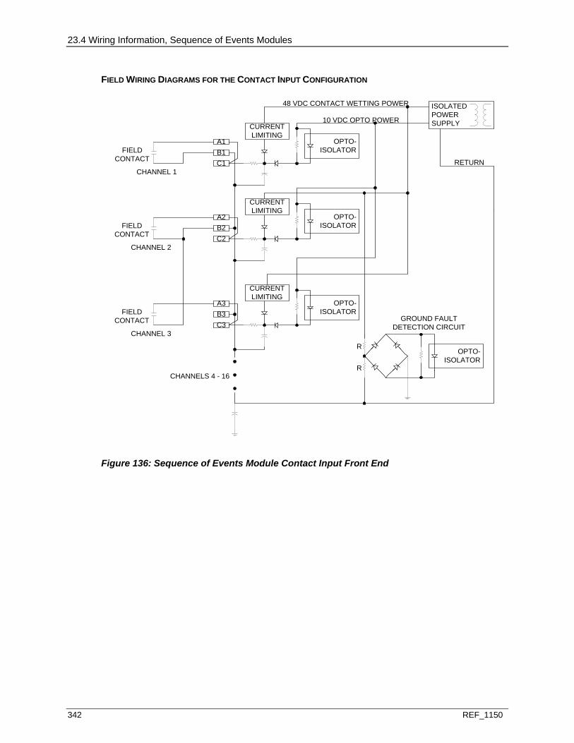
23.4 Wiring Information, Sequence of Events Modules
342 REF_1150
FIELD WIRING DIAGRAMS FOR THE CONTACT INPUT CONFIGURATION
ISOLATEDPOWERSUPPLY
OPTO-ISOLATOR
10 VDC OPTO POWERCURRENTLIMITING
48 VDC CONTACT WETTING POWER
OPTO-ISOLATOR
CURRENTLIMITING
A1B1C1
A2B2C2
FIELDCONTACT
FIELDCONTACT
CHANNELS 4 - 16
CHANNEL 1
CHANNEL 2
R
R
OPTO-ISOLATOR
GROUND FAULTDETECTION CIRCUIT
OPTO-ISOLATOR
CURRENTLIMITING
A3B3C3
FIELDCONTACT
CHANNEL 3
RETURN
Figure 136: Sequence of Events Module Contact Input Front End
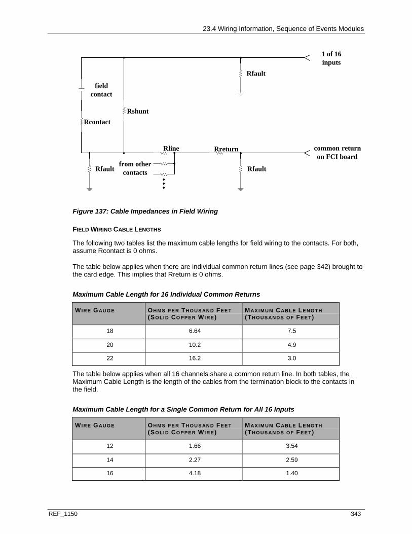
23.4 Wiring Information, Sequence of Events Modules
REF_1150 343
fieldcontact
RcontactRshunt
Rfault
Rline
from othercontacts
Rreturn
Rfault
Rfault
1 of 16inputs
common returnon FCI board
Figure 137: Cable Impedances in Field Wiring
FIELD WIRING CABLE LENGTHS
The following two tables list the maximum cable lengths for field wiring to the contacts. For both, assume Rcontact is 0 ohms.
The table below applies when there are individual common return lines (see page 342) brought to the card edge. This implies that Rreturn is 0 ohms.
Maximum Cable Length for 16 Individual Common Returns
WI RE GAU G E OHM S P E R TH O U S AN D FEE T (SO LI D CO PPE R WI RE)
MAX I M UM CABL E LE NG T H (THO U S AN D S O F FE E T)
18 6.64 7.5
20 10.2 4.9
22 16.2 3.0
The table below applies when all 16 channels share a common return line. In both tables, the Maximum Cable Length is the length of the cables from the termination block to the contacts in the field.
Maximum Cable Length for a Single Common Return for All 16 Inputs
WI RE GAU G E OHM S P E R TH O U S AN D FEE T (SO LI D CO PPE R WI RE)
MAX I M UM CABL E LE NG T H (THO U S AN D S O F FE E T)
12 1.66 3.54
14 2.27 2.59
16 4.18 1.40

23.4 Wiring Information, Sequence of Events Modules
344 REF_1150
WI RE GAU G E OHM S P E R TH O U S AN D FEE T (SO LI D CO PPE R WI RE)
MAX I M UM CABL E LE NG T H (THO U S AN D S O F FE E T)
18 6.64 0.89
Sequence of Events Contact Input Terminal Block Wiring Information
The diagram for the Sequence of Events contact input Personality module is illustrated in the figure below.
Figure 138: Terminal Block Connections for the Sequence of Events Contact Input Personality Modules
The following table lists and defines the abbreviations used in this diagram.
Abbreviations Used in Diagrams
AB B R E V I AT I ON DE FI NI T I O N
1+ through 16+ Contact input positive terminal connection.
1- through 16- Contact input negative terminal connection.
Earth ground terminals.
PS+, PS- Auxiliary Power Supply terminals.
RSV Reserved terminal. No connection allowed on these terminals.
Note: Do not use terminal block locations marked RSV.

23.4 Wiring Information, Sequence of Events Modules
REF_1150 345
SEQUENCE OF EVENTS CONTACT INPUT FIELD CONNECTION WIRING DIAGRAM (NON-CE MARK)
1C31110G03
1C31110G03
ElectronicsModule
ElectronicsModule
Figure 139: Field Connection for the SOE Contact Input Pmod (Non-CE Mark)

23.4 Wiring Information, Sequence of Events Modules
346 REF_1150
SEQUENCE OF EVENTS CONTACT INPUT FIELD CONNECTION WIRING DIAGRAM (CE MARK)
Field
See Note 1
Contacts16
1+
1-
16+
16-
In1
In16
Personality Module ElectronicsModule1C31110G03
All field wiring must be braid-shielded and grounded at the entry point of the cabinet using
Note
the recommended hardware (refer to "Cable Guidelines" in the applicable Ovation system
ChannelRtn
Personality Module ElectronicsModule1C31110G03
FieldContacts
16
1+
16+
x-
In1
In16
ChannelRtn
x- = one input fromthe set {1-,...16-}
installation manual).
Figure 140: Field Connection for the SOE Contact Input Pmod (CE Mark)
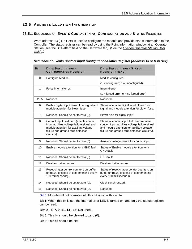
23.5 Address Location Information
REF_1150 347
23.5 ADDRESS LOCATION INFORMATION
23.5.1 SEQUENCE OF EVENTS CONTACT INPUT CONFIGURATION AND STATUS REGISTER
Word address 13 (D in Hex) is used to configure the module and provide status information to the Controller. The status register can be read by using the Point Information window at an Operator Station (see the Bit Pattern field on the Hardware tab). (See the Ovation Operator Station User Guide.)
Sequence of Events Contact Input Configuration/Status Register (Address 13 or D in Hex)
BI T DAT A DE S C R I P T I O N - CO N FI G U R AT I O N REGI S TE R
DAT A DE S C R I P T I O N - ST ATUS RE GI S T E R (RE AD)
0 Configure Module. Module configured
(1 = configured; 0 = unconfigured)
1 Force internal error. Internal error
(1 = forced error; 0 = no forced error)
2 - 5 Not used. Not used.
6 Enable digital input blown fuse signal and module attention for blown fuse.
Status of enable digital input blown fuse signal and module attention for blown fuse.
7 Not used. Should be set to zero (0). Blown fuse for digital input
8 Contact input field card (enable contact input auxiliary voltage failure signal and module attention for auxiliary voltage failure and ground fault detection circuitry).
Status of contact input field card (enable contact input auxiliary voltage failure signal and module attention for auxiliary voltage failure and ground fault detection circuitry).
9 Not used. Should be set to zero (0). Auxiliary voltage failure for contact input.
10 Enable module attention for a GND fault. Status of Enable module attention for a GND fault.
11 Not used. Should be set to zero (0). GND fault.
12 Disable chatter control. Disable chatter control.
13 Reset chatter control counters on buffer unfreeze (instead of decrementing every 100 milliseconds).
Status of reset chatter control counters on buffer unfreeze (instead of decrementing every 100 milliseconds).
14 Not used. Should be set to zero (0). Clock synchronized.
15 Not used. Should be set to zero (0). Not used.
Bit 0: Module will not operate until this bit is set with a write.
Bit 1: When this bit is set, the internal error LED is turned on, and only the status registers can be read.
Bits 2 - 5, 7, 9, 11, 14 - 15: Not used.
Bit 6: This bit should be cleared to zero (0).
Bit 8: This bit should be set.
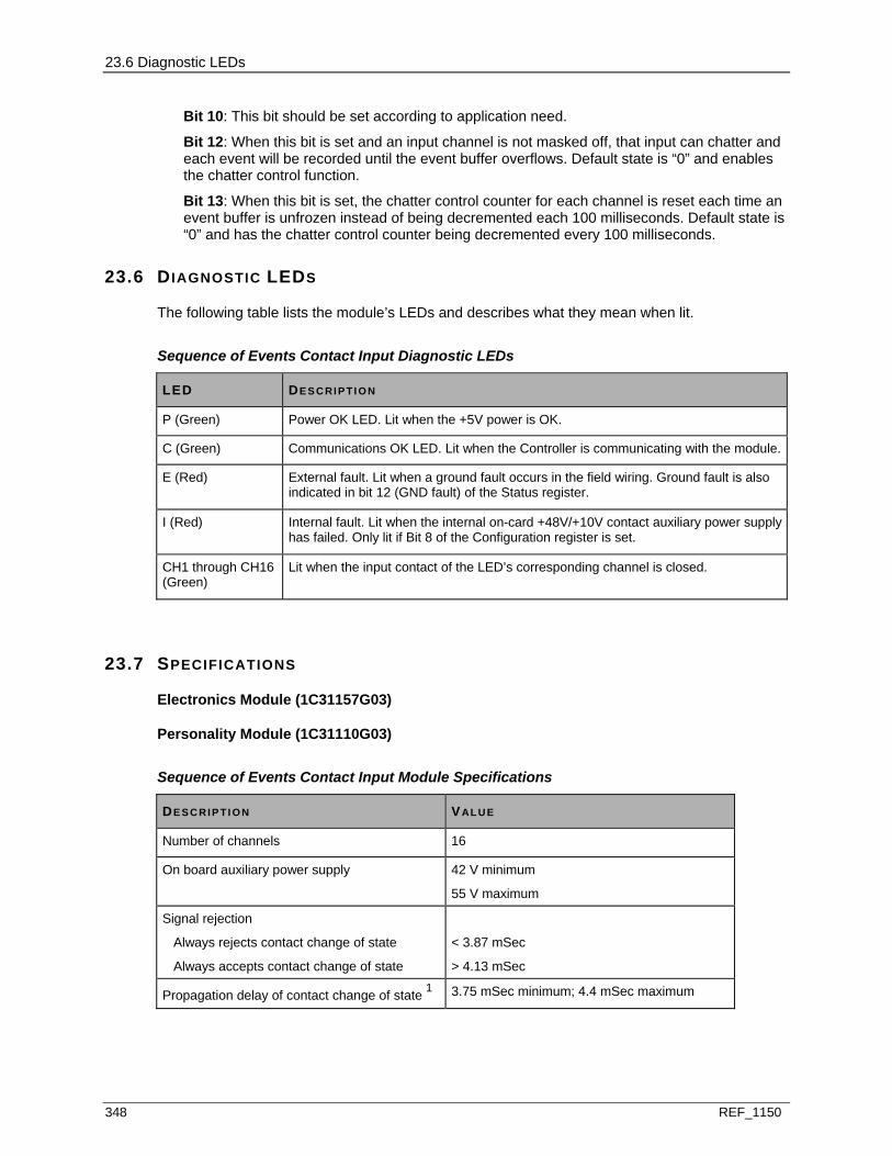
23.6 Diagnostic LEDs
348 REF_1150
Bit 10: This bit should be set according to application need.
Bit 12: When this bit is set and an input channel is not masked off, that input can chatter and each event will be recorded until the event buffer overflows. Default state is “0” and enables the chatter control function.
Bit 13: When this bit is set, the chatter control counter for each channel is reset each time an event buffer is unfrozen instead of being decremented each 100 milliseconds. Default state is “0” and has the chatter control counter being decremented every 100 milliseconds.
23.6 DIAGNOSTIC LEDS
The following table lists the module’s LEDs and describes what they mean when lit.
Sequence of Events Contact Input Diagnostic LEDs
LED DE S C RI P TI O N
P (Green) Power OK LED. Lit when the +5V power is OK.
C (Green) Communications OK LED. Lit when the Controller is communicating with the module.
E (Red) External fault. Lit when a ground fault occurs in the field wiring. Ground fault is also indicated in bit 12 (GND fault) of the Status register.
I (Red) Internal fault. Lit when the internal on-card +48V/+10V contact auxiliary power supply has failed. Only lit if Bit 8 of the Configuration register is set.
CH1 through CH16 (Green)
Lit when the input contact of the LED’s corresponding channel is closed.
23.7 SPECIFICATIONS
Electronics Module (1C31157G03)
Personality Module (1C31110G03)
Sequence of Events Contact Input Module Specifications
DE S C RI P TI O N VAL UE
Number of channels 16
On board auxiliary power supply 42 V minimum
55 V maximum
Signal rejection
Always rejects contact change of state
Always accepts contact change of state
< 3.87 mSec
> 4.13 mSec
Propagation delay of contact change of state 1 3.75 mSec minimum; 4.4 mSec maximum
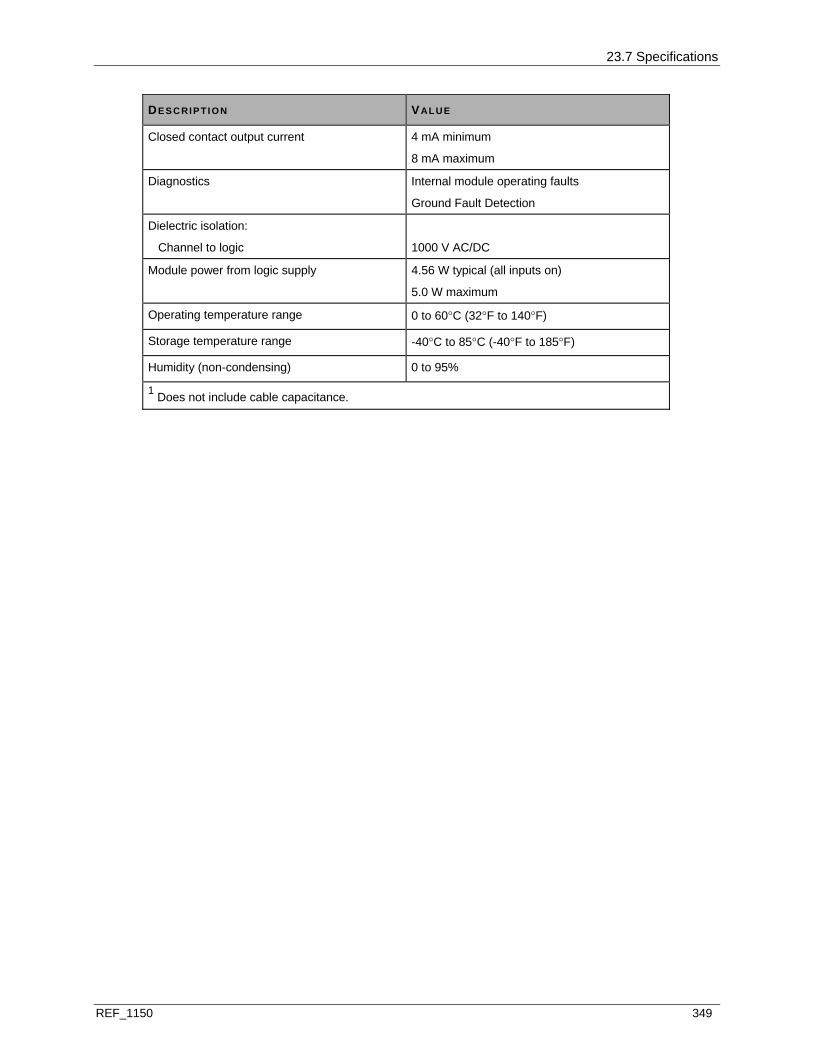
23.7 Specifications
REF_1150 349
DE S C RI P TI O N VAL UE
Closed contact output current 4 mA minimum
8 mA maximum
Diagnostics Internal module operating faults
Ground Fault Detection
Dielectric isolation:
Channel to logic
1000 V AC/DC
Module power from logic supply 4.56 W typical (all inputs on)
5.0 W maximum
Operating temperature range 0 to 60°C (32°F to 140°F)
Storage temperature range -40°C to 85°C (-40°F to 185°F)
Humidity (non-condensing) 0 to 95%
1 Does not include cable capacitance.

REF_1150 351
IN THIS SECTION
Description ......................................................................................................................352 Module Group Information ..............................................................................................353 Module Specific Information............................................................................................354 Wiring Information, Sequence of Events Modules..........................................................355 Diagnostic LEDs..............................................................................................................371 Specifications ..................................................................................................................371
S E C T I O N 2 4
COMPACT SEQUENCE OF EVENTS MODULE
24.1 Description
352 REF_1150
24.1 DESCRIPTION
The Compact Sequence of Events (SOE) module provides 16 digital channels to monitor the open or closed state of digital inputs or contacts in the field. The module provides a filter to reject changes of state less than four milliseconds. The Compact Sequence of Events module can also perform event tagging and chatter control for each input channel.
The Ovation Controller writes a channel event tagging mask to the Electronics module to enable event tagging for specific input channels. It has a chatter control flag for each channel to indicate that the input channel has changed state too many times in a period of time, or is changing state at too fast a rate. It also has a channel ID to indicate which channel changed state. Each channel is checked every 125 micro-seconds. If the channel event tagging mask bit is zero, that channel is not checked.
If there is an input channel state change, the change is recorded in the SOE module’s Event Buffer and the input channel’s Chatter counter is incremented. When the input channel’s Chatter counter value reaches four, any additional state changes are not recorded for that input channel. The recording of additional state changes for that input channel is inhibited until the input channel Chatter counter is reset to a zero value.
A control bit written by the Ovation Controller provides two options for resetting an input channel’s Chatter counter:
Each input channel’s Chatter counter is reset after the Ovation Controller reads the SOE module’s Event Buffer. With this option selected, the SOE module will identify up to four state changes for each of its input channels between successive Ovation Controller Event Buffer read operations.
Each input channel’s Chatter counter is checked every 100 milliseconds and is decremented if its value is greater than zero. When the input channel’s Chatter counter value reaches zero, future input channel state changes may be entered into the Event Buffer. With this option selected, an input state change rate greater than 1 per 100 milliseconds will result in no new Event Buffer entries for that input channel while a lower input state change rate will allow new Event Buffer entries for that input channel.
The Compact Sequence of Events module is applicable for CE Mark certified systems.
There are two 32 event buffers. This allows the event tagging and chatter control function to be writing into one event buffer while the Ovation Controller is reading the other event buffer. The Ovation Controller only reads each module a small portion of the loop time. This allows both event buffers to be available the rest of the loop time.
Each event buffer contains 64 words with up to 32 Channel-IDs and 32 Event-Times. The event buffers are memories. The memory control circuit controls which event buffer to write into and which event buffer to read from. Before reading the event buffer, the buffer status register must be read to determine the number of words to read.
Time synchronization is accomplished by the Ovation Controller writing a time reference simultaneously to all Sequence of Events modules with a 1 millisecond resolution. The Compact Sequence of Event Module is CE Mark applicable.
Note: I/O Module General Information (see page 15) contains environmental, installation, wiring, and fuse information for I/O modules. All SOE modules in a Controller MUST be connected to the IOIC card that is configured as the Time Keeper.

24.2 Module Group Information
REF_1150 353
CAUTION! Do NOT mix the Compact Sequence of Events module (1C31233) with the Sequence of Events module (1C31157) in the same system.
CAUTION! CE Mark certified systems: Any base unit that contains a 125VDC Compact Sequence of Events Electronics module (1C31233G03) with Foam Insert (1C31238H01) and interfaces to hazardous voltage (>60 VDC) must include a hazardous voltage warning label (1B30025H01) on that base unit. Any base unit containing a 125VDC Compact Sequence of Events Electronics module (1C31233G03) with Fused Digital Input Personality module (5X00034G01) and interfaces to hazardous voltage (>60 VDC) must include a hazardous voltage warning label (1B30025H01) on ALL base units on the branch. This label must be placed in a visible location on the base unit, preferably above the spare fuse location. The project drawings must indicate this.
The Sequence of Events module comes in five combinations of Electronics and Personality Modules:
24/48 VDC single-ended digital input. 24/48 VDC differential input. 125 VDC single-ended digital input. 125 VDC differential input. 48 VDC contact input with on card auxiliary supply.
24.2 MODULE GROUP INFORMATION
24.2.1 ELECTRONICS MODULES (EMODS)
There are four Electronics module groups for the Compact Sequence of Events Module:
1C31233G01 provides for 24/48 VDC single-ended inputs. 1C31233G02 provides for 24/48 VDC differential inputs and supports the 16 point individually
fused option. 1C31233G03 provides for 125 VDC differential inputs and supports the 16 point individually
fused option. 1C31233G04 (Contact Input) provides for 48 VDC on-card auxiliary power.
Personality Module (Pmods)
There is one Personality module group for the Compact Sequence of Events Module:
5X00034G01 provides for 16 point individual fusing with a common supply.
This is an optional Personality module that is available for use with the differential input Electronics modules (1C31233G02, 1C31233G03) for applications requiring individual point fusing with a common supply.
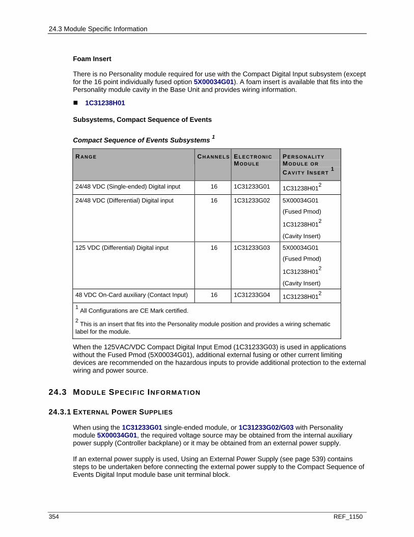
24.3 Module Specific Information
354 REF_1150
Foam Insert
There is no Personality module required for use with the Compact Digital Input subsystem (except for the 16 point individually fused option 5X00034G01). A foam insert is available that fits into the Personality module cavity in the Base Unit and provides wiring information.
1C31238H01
Subsystems, Compact Sequence of Events
Compact Sequence of Events Subsystems 1
RANG E CH AN N E L S EL E CT RO NI C MO D U LE
PE R S O N AL I T Y MO D U LE O R
CAV I T Y INSERT 1
24/48 VDC (Single-ended) Digital input 16 1C31233G01 1C31238H012
24/48 VDC (Differential) Digital input 16 1C31233G02 5X00034G01
(Fused Pmod)
1C31238H012
(Cavity Insert)
125 VDC (Differential) Digital input 16 1C31233G03 5X00034G01
(Fused Pmod)
1C31238H012
(Cavity Insert)
48 VDC On-Card auxiliary (Contact Input) 16 1C31233G04 1C31238H012 1 All Configurations are CE Mark certified. 2 This is an insert that fits into the Personality module position and provides a wiring schematic label for the module.
When the 125VAC/VDC Compact Digital Input Emod (1C31233G03) is used in applications without the Fused Pmod (5X00034G01), additional external fusing or other current limiting devices are recommended on the hazardous inputs to provide additional protection to the external wiring and power source.
24.3 MODULE SPECIFIC INFORMATION
24.3.1 EXTERNAL POWER SUPPLIES
When using the 1C31233G01 single-ended module, or 1C31233G02/G03 with Personality module 5X00034G01, the required voltage source may be obtained from the internal auxiliary power supply (Controller backplane) or it may be obtained from an external power supply.
If an external power supply is used, Using an External Power Supply (see page 539) contains steps to be undertaken before connecting the external power supply to the Compact Sequence of Events Digital Input module base unit terminal block.

24.4 Wiring Information, Sequence of Events Modules
REF_1150 355
24.4 WIRING INFORMATION, SEQUENCE OF EVENTS MODULES
The Sequence of Events modules can be divided into two types depending on their front end connections, Digital Input Field Interface or Contact Filed Interface. The digital Input field Interface modules can be broken down further into Single-Ended and Differential as well as low and high voltage.
The following wiring section topics will be split to show the wiring of the Sequence of Events Digital Input Field Interface modules, then the Sequence of Events Contact Filed Interface modules.
24.4.1 SEQUENCE OF EVENTS DIGITAL INPUT FIELD INTERFACE MODULES
Digital Input Field Interface
The Digital Input configuration contains 16 channels, where each channel has voltage level sensing circuitry used to detect whether an input is on or off. Style 1C31233G02/G03 has 16 isolated differential inputs to accommodate separate external auxiliary supplies. Style 1C31233G01 has 16 single-ended (common return) digital inputs with an on-card blown fuse detect to accommodate a common external auxiliary supply for all channels. The input voltage level monitored by the module is determined by the particular card group in the module.
Also, Style 1C31233G02/G03 can be used with the individually fused Personality module 5X00034G01 for applications requiring individual point fusing with a common supply.
An input resistor provides the normal mode surge protection and limits the current during normal operation. An opto-isolator provides high dielectric isolation between the field side and the logic or I/O bus side. The Single-Ended Digital Input configuration has a circuit used to monitor the presence of the wetting supply. Two cases cause this monitor circuitry to report a blown fuse status and issue an attention status to the Ovation Controller:
Fuse is blown on the module. Auxiliary supply level is lower than minimum On Input Voltage.
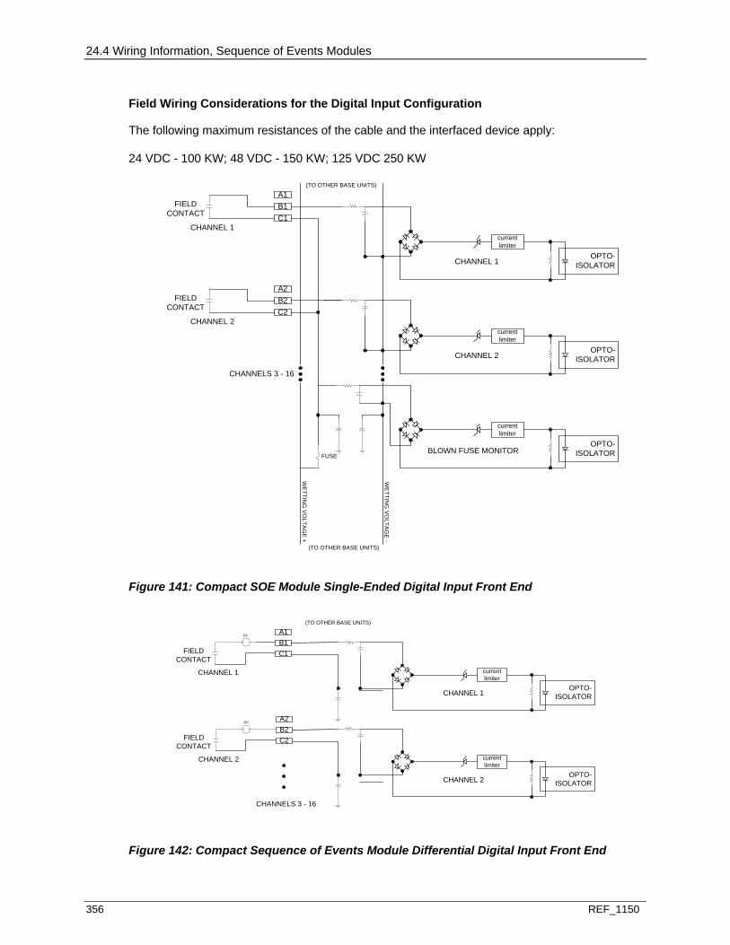
24.4 Wiring Information, Sequence of Events Modules
356 REF_1150
Field Wiring Considerations for the Digital Input Configuration
The following maximum resistances of the cable and the interfaced device apply:
24 VDC - 100 KW; 48 VDC - 150 KW; 125 VDC 250 KW
OPTO-ISOLATOR
A1B1C1
FIELDCONTACT
CHANNEL 1currentlimiter
OPTO-ISOLATOR
currentlimiter
A2B2C2
FIELDCONTACT
CHANNEL 2
CHANNELS 3 - 16
WETTIN
G V
OLTAG
E +
WE
TTING
VO
LTAGE
-
(TO OTHER BASE UNITS)
(TO OTHER BASE UNITS)
FUSE
OPTO-ISOLATOR
currentlimiter
CHANNEL 1
CHANNEL 2
BLOWN FUSE MONITOR
Figure 141: Compact SOE Module Single-Ended Digital Input Front End
OPTO-ISOLATOR
A1B1C1FIELD
CONTACT
CHANNEL 1 currentlimiter
OPTO-ISOLATOR
currentlimiter
A2B2C2FIELD
CONTACT
CHANNEL 2
CHANNELS 3 - 16
(TO OTHER BASE UNITS)
CHANNEL 1
CHANNEL 2
DC
DC
Figure 142: Compact Sequence of Events Module Differential Digital Input Front End

24.4 Wiring Information, Sequence of Events Modules
REF_1150 357
Figure 143: 16 Individually Fused Compact Digital Inputs Front End
Compact SOE Digital Input Module Emod (1C31233G01 through G03)
Compact Sequence of Events Digital Input Specifications
DE S C RI P TI O N VAL UE
Number of channels 16
Input range (single-ended or differential) 1 Refer to the table below.
Propagation delay of contact change of state 2
24V/48V DC
125VDC
3.75 mSec minimum; 4.25 mSec maximum
3.75 mSec minimum; 4.45 mSec maximum
Signal rejection
Always rejects change of state
Always accepts change of state
< 3.87 mSec
> 4.13 mSec
Cable length (quality is 50pF/ft or better) 1000 feet maximum
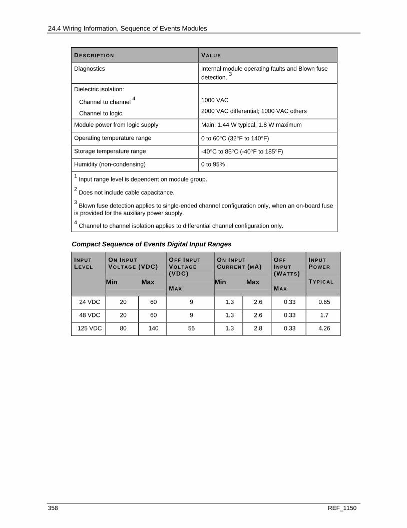
24.4 Wiring Information, Sequence of Events Modules
358 REF_1150
DE S C RI P TI O N VAL UE
Diagnostics Internal module operating faults and Blown fuse detection. 3
Dielectric isolation:
Channel to channel 4
Channel to logic
1000 VAC
2000 VAC differential; 1000 VAC others
Module power from logic supply Main: 1.44 W typical, 1.8 W maximum
Operating temperature range 0 to 60°C (32°F to 140°F)
Storage temperature range -40°C to 85°C (-40°F to 185°F)
Humidity (non-condensing) 0 to 95%
1 Input range level is dependent on module group. 2 Does not include cable capacitance. 3 Blown fuse detection applies to single-ended channel configuration only, when an on-board fuse is provided for the auxiliary power supply. 4 Channel to channel isolation applies to differential channel configuration only.
Compact Sequence of Events Digital Input Ranges
IN P U T LEV E L
ON INP UT VO L T AG E (VDC)
Min Max
OF F INP UT VO L T AG E (VDC)
MAX
ON INP UT CU R R E N T (MA)
Min Max
OF F IN P U T (WAT T S)
MAX
IN P U T PO WE R
TYPI C AL
24 VDC 20 60 9 1.3 2.6 0.33 0.65
48 VDC 20 60 9 1.3 2.6 0.33 1.7
125 VDC 80 140 55 1.3 2.8 0.33 4.26

24.4 Wiring Information, Sequence of Events Modules
REF_1150 359
Compact SOE Digital Input Terminal Block Wiring Information
The available foam insert has a simplified wiring diagram label on top, which appears above the terminal block. This diagram indicates how the wiring from the field is to be connected to the terminal block in the base unit. The diagrams for the Compact Sequence of Events Digital Input module are illustrated below.
Figure 144: Terminal Block Connections for the Compact Sequence of Events Digital Input Module (1C31233G01 -G03)
AB B R E V I AT I ON DE FI NI T I O N
1+ through 16+ Digital input positive terminal connection
1- through 16- Digital input negative terminal connection
Earth ground terminals
PS+, PS- Auxiliary Power Supply terminals
RSV Reserved terminal. No internal connection

24.4 Wiring Information, Sequence of Events Modules
360 REF_1150
COMPACT SOE DIGITAL INPUT FIELD CONNECTION WIRING DIAGRAM (NON-CE MARK)
Field
Single-Ended Digital Voltage Inputs
Contacts16
PS+
PS-
1-
1+
16-
16+
Rtn1
In1
Rtn16
In16
PowerMonitor
Rtn
Electronics Module
SurgeProtection
AuxiliaryVoltageSupply
0.5A
Field
Differential Digital Voltage Inputs
Devices
1-
1+
16-
16+
Rtn1
In1
Rtn16In16
AuxiliaryVoltageSupplies
16
Field
16 Individually Fused Digital Voltage Inputs
Contacts16
PS+
PS-
1+
1-
In1
Rtn1
In2
AuxiliaryVoltageSupply
0.5A
Rtn2
0.5A
16+
16-
Electronics Module
Electronics ModulePersonality Module
Channel1
Rtn1
In1Channel16
Rtn1
In1Channel
1
Rtn1
In1Channel
16
Rtn1
In1Channel
1
Rtn1
In1Channel
16
* Auxiliary power supply may be AC or DC. It a DC supply is used, the polarity can be opposite of what is shown.
*
*
Figure 145: Field Connection for the Compact Sequence of Events Digital Input Module (Non-CE Mark)

24.4 Wiring Information, Sequence of Events Modules
REF_1150 361
COMPACT SOE DIGITAL INPUT FIELD CONNECTION WIRING DIAGRAM (CE MARK)
Field
Single-Ended Digital Voltage Inputs
Contacts16
PS+
PS-
1-
1+
16-
16+
Rtn1
In1
Rtn16
In16
PowerMonitor
Rtn
Electronics Module
SurgeProtection
AuxiliaryVoltageSupply
0.5A
Field
Differential Digital Voltage Inputs
Devices
1-
1+
16-
16+
Rtn1
In1
Rtn16
In16AuxiliaryVoltageSupplies
16
Field
16 Individually Fused Digital Voltage Inputs
Contacts16
PS+
PS-
1+
1-
In1
Rtn1
In2
AuxiliaryVoltageSupply
0.5A
Rtn2
0.5A
16+
16-
Electronics Module
Electronics ModulePersonality Module
All field wiring must be braid-shielded and grounded at entry point of cabinet using recommended hardware (refer to "CableGuidelines" in the applicableOvation installation manual).
Rtn1
In1Channel
1
Rtn1
In1Channel16
Rtn1
In1Channel
1
Rtn1
In1Channel
16
Rtn1
In1Channel
1
Rtn1
In1Channel
16
*
*
* Auxiliary power supply may be AC or DC. It a DC supply is used, the polarity can be opposite of what is shown.
Figure 146: Field Connection for the Compact Sequence of Events Digital Input Module (CE Mark)

24.4 Wiring Information, Sequence of Events Modules
362 REF_1150
ADDRESS LOCATION INFORMATION 24.4.1.1.1.1 Compact SOE Digital Input Configuration and Status Register Word address 13 (D in Hex) is used to configure the module and provide status information to the Controller. The status register can be read by using the Point Information window at an Operator Station (see the Bit Pattern Field on the Hardware Tab). Refer to the applicable “Operator Station User Guide” for information about the Point Information window.
Compact Sequence of Events Digital Input Configuration/Status Register (Address 13 or D in Hex)
BI T DAT A DE S C R I P T I O N - CO NF I G U R AT I O N RE GI S T E R (WRI T E)
DAT A DE S C R I P T I O N - ST ATUS REGI S TER (RE AD)
0 Configure Module. Module configured
(1 = configured; 0 = not configured)
1 Force internal error. Internal error
(1 = forced error; 0 = no forced error)
2 - 5 Not used. Should be set to zero (0). Not used.
6 Enable digital input blown fuse signal and module attention for blown fuse.
Status of enable digital input blown fuse signal and module attention for blown fuse.
7 Not used. Should be set to zero (0). Blown fuse for digital input.
8 Contact input field card (enable contact input auxiliary voltage failure signal and module attention for auxiliary voltage failure and ground fault detection circuitry).
Status of contact input field card (enable contact input auxiliary voltage failure signal and module attention for auxiliary voltage failure and ground fault detection circuitry).
9 Not used. Should be set to zero (0). Auxiliary voltage failure for contact input
10 Enable module attention for a GND fault. Status of Enable module attention for a GND fault.
11 Not used. Should be set to zero (0). GND fault.
12 Disable chatter control. Disable chatter control.
13 Chatter control option. Status of chatter control option.
14 Not used. Should be set to zero (0). Clock synchronized.
15 Not used. Should be set to zero (0). Not used.
1 Applicable for configuration of the Digital Input module (1C31233G01 - G03).
Bit 0: Module will not operate until this bit is set with a write.
Bit 1: When this bit is set, the internal error LED is turned on, and only the status registers can be read.
Bits 2 - 5, 7, 11, 14 - 15: Not used.
Bit 6: This bit should be set for a single-ended digital input (1C31233G01) and cleared for the others.
Bits 8 - 10: These bits should be cleared to zero (0).
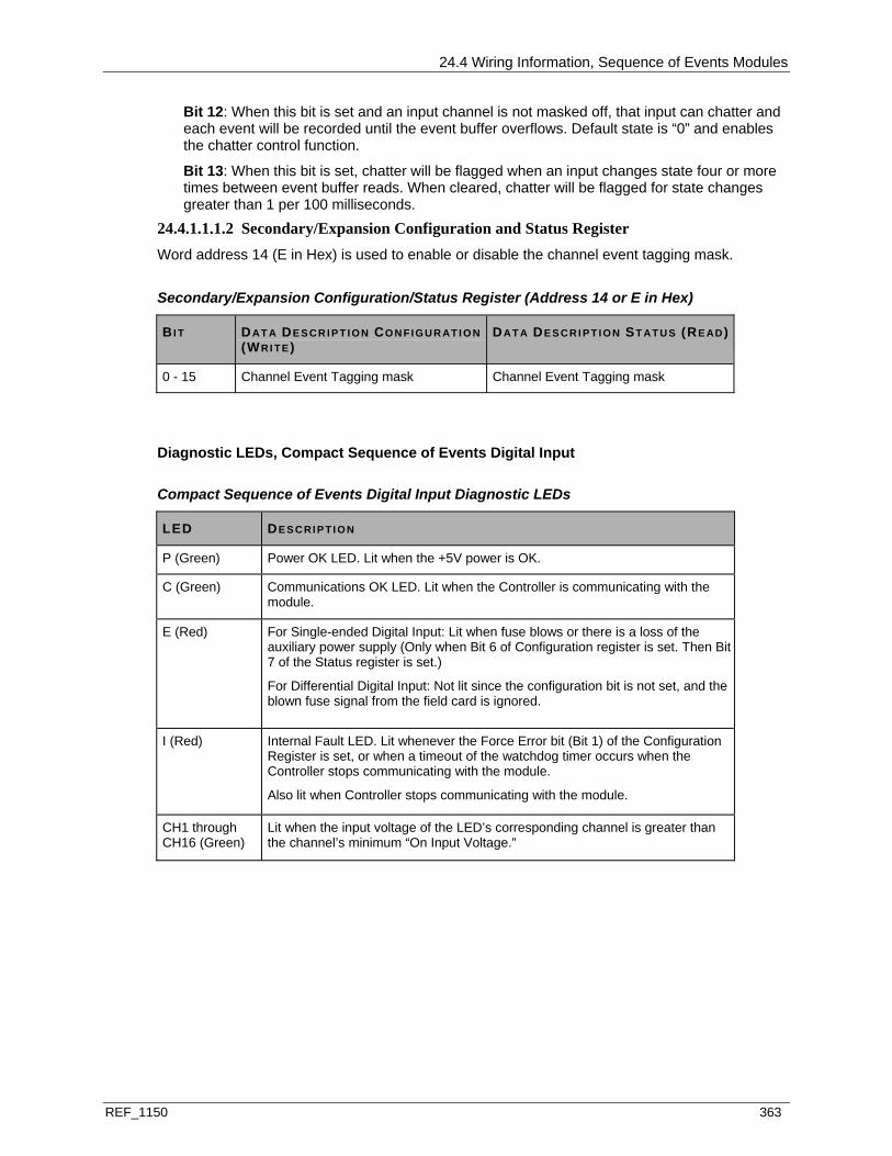
24.4 Wiring Information, Sequence of Events Modules
REF_1150 363
Bit 12: When this bit is set and an input channel is not masked off, that input can chatter and each event will be recorded until the event buffer overflows. Default state is “0” and enables the chatter control function.
Bit 13: When this bit is set, chatter will be flagged when an input changes state four or more times between event buffer reads. When cleared, chatter will be flagged for state changes greater than 1 per 100 milliseconds.
24.4.1.1.1.2 Secondary/Expansion Configuration and Status Register Word address 14 (E in Hex) is used to enable or disable the channel event tagging mask.
Secondary/Expansion Configuration/Status Register (Address 14 or E in Hex)
BI T DAT A DE S C R I P T I O N CO N FI G U R AT I O N (WRI TE)
DAT A DE S C R I P T I O N ST ATUS (RE AD)
0 - 15 Channel Event Tagging mask Channel Event Tagging mask
Diagnostic LEDs, Compact Sequence of Events Digital Input
Compact Sequence of Events Digital Input Diagnostic LEDs
LED DE S C RI P TI O N
P (Green) Power OK LED. Lit when the +5V power is OK.
C (Green) Communications OK LED. Lit when the Controller is communicating with the module.
E (Red) For Single-ended Digital Input: Lit when fuse blows or there is a loss of the auxiliary power supply (Only when Bit 6 of Configuration register is set. Then Bit 7 of the Status register is set.)
For Differential Digital Input: Not lit since the configuration bit is not set, and the blown fuse signal from the field card is ignored.
I (Red) Internal Fault LED. Lit whenever the Force Error bit (Bit 1) of the Configuration Register is set, or when a timeout of the watchdog timer occurs when the Controller stops communicating with the module.
Also lit when Controller stops communicating with the module.
CH1 through CH16 (Green)
Lit when the input voltage of the LED’s corresponding channel is greater than the channel’s minimum “On Input Voltage.”

24.4 Wiring Information, Sequence of Events Modules
364 REF_1150
24.4.2 SEQUENCE OF EVENTS CONTACT FIELD INTERFACE MODULES
Compact SOE Contact Input Field Interface
The Contact Input configuration (1C31233G04) provides 16 contact input current detecting channels with common returns. The field side circuitry and terminal connections for three of these channels are shown in the figure below.
A +48V on-board power supply provides current limited contact wetting voltage if the contact is open. If the contact closes, current is drawn from the +10V supply which turns on the associated opto-isolator; thereby, relaying a closed contact state to the I/O bus. The opto-isolators and the isolation provided by the 10V and 48 Volt power supply provide high dielectric isolation between the field side and the logic or I/O bus side.
There are two methods of wiring field devices to the termination block as shown in the figure below. Each field contact may have a separate input and return line as shown for channel 1. Alternatively, field contacts wired to the same module may share a return line as shown for channels 2 and 3. For either wiring method, do not tie the contact return line to earth ground or a ground fault condition will occur, as well as a degradation of the common mode surge protection.
Ground fault detection circuitry on the Sequence of Events module with Contact Inputs activates when the input or return line for any channel finds a low impedance (<5 K ohms) path to earth ground. A single wire with a ground fault will not cause an error in the point data, but multiple ground faults, if they include input and return lines, could cause faulty data (that is, channels appearing as if their contacts are closed when they are really open).
When a ground fault occurs, the external error LED lights, and the GND Fault bit 11 in the Status Register is set. If the GND Fault Attention Enable bit 8 is set in the Configuration Register, a ground fault is seen as a catastrophic error causing an attention status to be sent back to the Controller. See the figure below for ground fault detection circuitry.

24.4 Wiring Information, Sequence of Events Modules
REF_1150 365
ISOLATEDPOWERSUPPLY
OPTO-ISOLATOR
10 VDC OPTO POWERCURRENTLIMITING
48 VDC CONTACT WETTING POWER
OPTO-ISOLATOR
CURRENTLIMITING
A1B1C1
A2B2C2
FIELDCONTACT
FIELDCONTACT
CHANNELS 4 - 16
CHANNEL 1
CHANNEL 2
R
R
OPTO-ISOLATOR
GROUND FAULTDETECTION CIRCUIT
OPTO-ISOLATOR
CURRENTLIMITING
A3B3C3
FIELDCONTACT
CHANNEL 3
RETURN
Figure 147: Compact Sequence of Events Module Contact Input Front End
Field Wiring Considerations for the Contact Input Configuration
The following definitions apply to the restrictions listed below:
Rshunt = contact shunt resistance
Rcontact = resistance associated with a closed contact
Rreturn = resistance of the common return line
Rline = resistance of the non-common cable length to and from the contact
Rwiring = Rcontact + Rline + 16Rreturn
Rfault = resistance from either line to ground which causes a ground fault
The figure below shows possible cable resistances that affect contact input performance. The following restrictions apply:
Under no-ground-fault conditions or if the channel return (low) line has a ground fault: Rshunt across contact must be greater than or equal to 10k ohms to always recognize
an open contact as open.
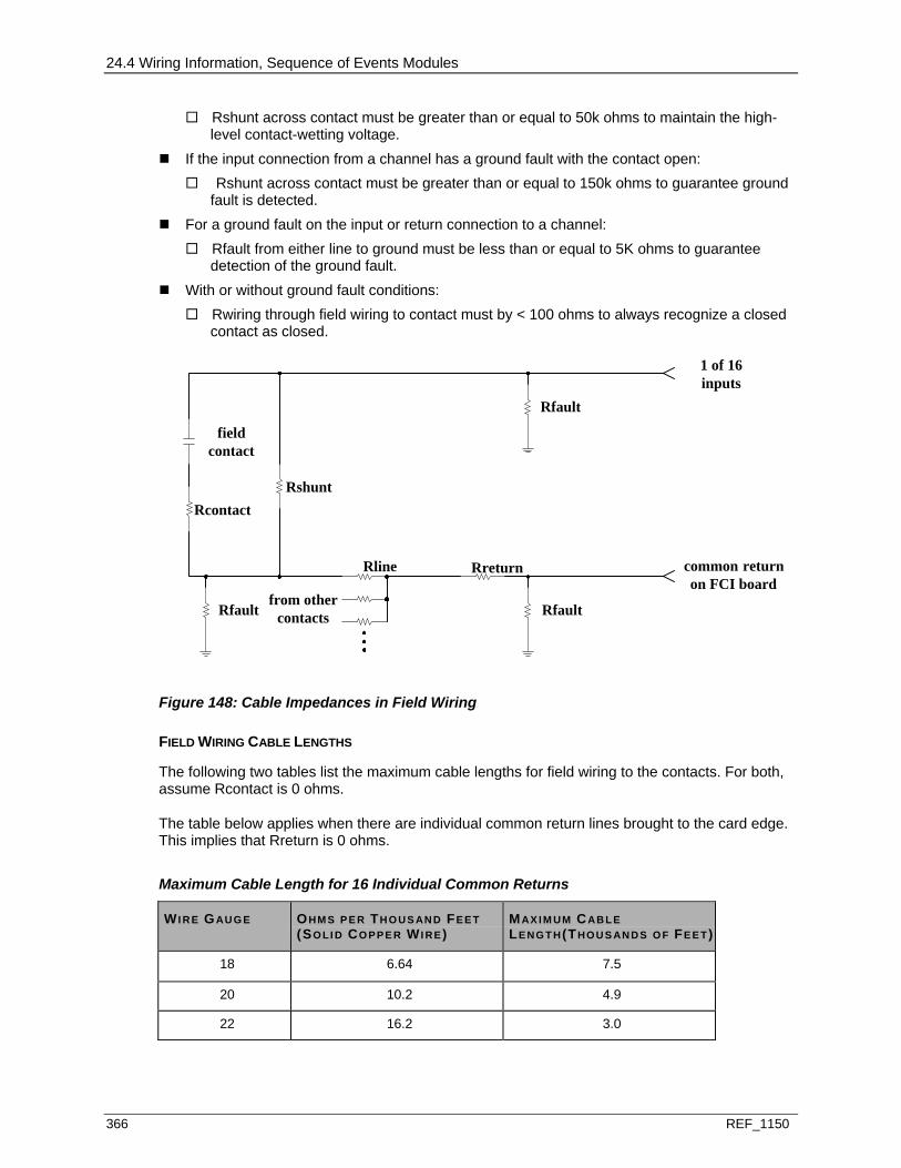
24.4 Wiring Information, Sequence of Events Modules
366 REF_1150
Rshunt across contact must be greater than or equal to 50k ohms to maintain the high-level contact-wetting voltage.
If the input connection from a channel has a ground fault with the contact open: Rshunt across contact must be greater than or equal to 150k ohms to guarantee ground
fault is detected. For a ground fault on the input or return connection to a channel:
Rfault from either line to ground must be less than or equal to 5K ohms to guarantee detection of the ground fault.
With or without ground fault conditions: Rwiring through field wiring to contact must by < 100 ohms to always recognize a closed
contact as closed.
fieldcontact
RcontactRshunt
Rfault
Rline
from othercontacts
Rreturn
Rfault
Rfault
1 of 16inputs
common returnon FCI board
Figure 148: Cable Impedances in Field Wiring
FIELD WIRING CABLE LENGTHS
The following two tables list the maximum cable lengths for field wiring to the contacts. For both, assume Rcontact is 0 ohms.
The table below applies when there are individual common return lines brought to the card edge. This implies that Rreturn is 0 ohms.
Maximum Cable Length for 16 Individual Common Returns
WI RE GAU G E OHM S P E R TH O U S AN D FEE T (SO LI D CO PPE R WI RE)
MAX I M UM CABL E LE NG T H(THOU S AN D S O F FE E T)
18 6.64 7.5
20 10.2 4.9
22 16.2 3.0

24.4 Wiring Information, Sequence of Events Modules
REF_1150 367
The table below applies when all 16 channels share a common return line. In both tables, the Maximum Cable Length is the length of the cables from the termination block to the contacts in the field.
Maximum Cable Length for a Single Common Return for All 16 Inputs
WI RE GAU G E OHM S P E R TH O U S AN D FEE T (SO LI D CO PPE R WI RE)
MAX I M UM CABLE LE NG T H (THO U S AN D S O F FE E T)
12 1.66 3.54
14 2.27 2.59
16 4.18 1.40
18 6.64 0.89
Compact SOE Contact Input Terminal Block Wiring Information
The diagram for the Compact Sequence of Events Contact Input module is illustrated below. The following table lists and defines the abbreviations used in this diagram.
Figure 149: Terminal Block Connections for the Compact Sequence of Events Contact Input Modules (1C31233G04)
Abbreviations Used in Diagrams
AB B R E V I AT I ON DE FI NI T I O N
1+ through 16+ Contact input positive terminal connection
1- through 16- Contact input negative terminal connection
Earth ground terminals
PS+, PS- Auxiliary Power Supply terminals
RSV Reserved terminal. No internal connection
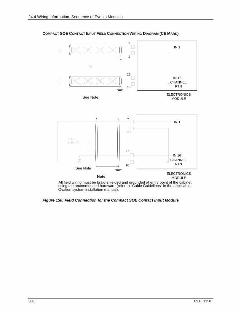
24.4 Wiring Information, Sequence of Events Modules
368 REF_1150
COMPACT SOE CONTACT INPUT FIELD CONNECTION WIRING DIAGRAM (CE MARK)
IN 1
IN 16CHANNEL
RTN
ELECTRONICSMODULE
IN 1
IN 16CHANNEL
RTN
ELECTRONICSMODULE
1
1
16
16
1
1
16
16
Note
See Note
See Note
using the recommended hardware (refer to "Cable Guidelines" in the applicableOvation system installation manual).
All field wiring must be braid-shielded and grounded at entry point of the cabinet
Figure 150: Field Connection for the Compact SOE Contact Input Module

24.4 Wiring Information, Sequence of Events Modules
REF_1150 369
COMPACT SOE CONTACT INPUT FIELD CONNECTION WIRING DIAGRAM (NON-CE MARK)
IN 1
IN 16CHANNEL
RTN
ELECTRONICSMODULE
IN 1
IN 16CHANNEL
RTN
ELECTRONICSMODULE
1
1
16
16
1
1
16
16
Figure 151: Field Connection for the Compact SOE Contact Input Module
ADDRESS LOCATION INFORMATION 24.4.2.1.1.1 Compact SOE Contact Input Configuration and Status Register Word address 13 (D in Hex) is used to configure the module and provide status information to the Controller. The status register can be read by using the Point Information window at an Operator Station (see the Bit Pattern Field on the Hardware Tab). (See the Operator Station User Guide.)

24.4 Wiring Information, Sequence of Events Modules
370 REF_1150
Compact Sequence of Events Contact Input Configuration/Status Register 1 Address 13 or D in Hex)
Bit Data Description - Configuration Register
Data Description - Status Register (Read)
0 Configure Module. Module configured
(1=configured; 0=unconfigured)
1 Force internal error. Internal error
(1=forced error; 0=no forced error)
2 - 5 Not used. Not used.
6 Enable digital input blown fuse signal and module attention for blown fuse.
Status of enable digital input blown fuse signal and module attention for blown fuse.
7 Not used. Should be set to zero (0). Blown fuse for digital input.
8 Contact input field card (enable contact input auxiliary voltage failure signal and module attention for auxiliary voltage failure and ground fault detection circuitry).
Status of contact input field card (enable contact input auxiliary voltage failure signal and module attention for auxiliary voltage failure and ground fault detection circuitry).
9 Not used. Should be set to zero (0). Auxiliary voltage failure for contact input.
10 Enable module attention for a GND fault. Status of Enable module attention for a GND fault.
11 Not used. Should be set to zero (0). GND fault.
12 Disable chatter control. Disable chatter control.
13 Reset chatter control counters on buffer unfreeze (instead of decrementing every 100 milliseconds).
Status of reset chatter control counters on buffer unfreeze (instead of decrementing every 100 milliseconds).
14 Not used. Should be set to zero (0). Clock synchronized.
15 Not used. Should be set to zero (0). Not used.
1 Applicable for configuration of the Contact Input module (1C31233G04).
Bit 0: Module will not operate until this bit is set with a write.
Bit 1: When this bit is set, the internal error LED is turned on, and only the status registers can be read.
Bits 2 - 5: Not used.
Bit 6: This bit should be cleared to zero (0).
Bit 7: Not used.
Bit 8: This bit should be set.
Bit 9: Not used.
24.5 Diagnostic LEDs
REF_1150 371
Bit 10: This bit should be set according to application need.
Bit 11: Not used.
Bit 12: When this bit is set and an input channel is not masked off, that input can chatter and each event will be recorded until the event buffer overflows. Default state is “0” and enables the chatter control function.
Bit 13: When this bit is set, the chatter control counter for each channel is reset each time an event buffer is unfrozen instead of being decremented each 100 milliseconds. Default state is “0” and has the chatter control counter being decremented every 100 milliseconds.
Bits 14 - 15: Not used.
24.5 DIAGNOSTIC LEDS
The following table lists the module’s LEDs and describes what they mean when lit.
Compact Sequence of Events Contact Input Diagnostic LEDs
LED DE S C RI P TI O N
P (Green) Power OK LED. Lit when the +5V power is OK.
C (Green) Communications OK LED. Lit when the Controller is communicating with the module.
E (Red) External fault. Lit when a ground fault occurs in the field wiring. Ground fault is also indicated in bit 12 (GND fault) of the Status register.
I (Red) Internal fault. Lit when the internal on-card +48V/+10V contact auxiliary power supply has failed. Only lit if Bit 8 of the Configuration register is set.
CH1 through CH16
(Green)
Lit when the input contact of the LED’s corresponding channel is closed.
24.6 SPECIFICATIONS
Compact SOE Contact Input Module Emod (1C31233G04)
Compact Sequence of Events Contact Input Module Specifications
DE S C RI P TI O N VALUE
Number of channels 16
On board auxiliary power supply 42 V minimum
55 V maximum
Signal rejection
Always rejects contact change of state
Always accepts contact change of state
< 3.87 mSec
> 4.13 mSec
Propagation delay of contact change of state 1 3.75 mSec minimum; 4.4 mSec maximum

24.6 Specifications
372 REF_1150
DE S C RI P TI O N VALUE
Closed contact output current 4 mA minimum
8 mA maximum
Diagnostics Internal module operating faults
Ground Fault Detection
Dielectric isolation:
Channel to logic
1000 VAC
Module power from logic supply 4.56 W typical (all inputs on)
5.0 W maximum
Operating temperature range 0 to 60°C (32°F to 140°F)
Storage temperature range -40°C to 85°C (-40°F to 185°F)
1 Does not include cable capacitance.
REF_1150 373
IN THIS SECTION
Description ......................................................................................................................373 Operation.........................................................................................................................374 Module Groups................................................................................................................375 Module Specific Information............................................................................................376 Wiring Information ...........................................................................................................394 Address Location Information .........................................................................................399 Diagnostics......................................................................................................................403 Diagnostic LEDs..............................................................................................................404 Specifications ..................................................................................................................405
25.1 DESCRIPTION
Steam turbines are used in many electrical power generation plants. The electrical load on a steam turbine's electric generator fluctuates as the electric power consumption increases or decreases. The Digital Electro-Hydraulic (DEH) control system provides turbine control to adjust steam turbine shaft rotational speed in response to varying electric generator loads. Very large amounts of force are required to move valves on large turbines. Therefore, an interposing device is required between the DEH control system and the controlled valves.
The Ovation Servo Driver module provides an interface between an Ovation Controller and an electro-hydraulic servo valve actuator. Each controlled turbine valve is connected to an electro-hydraulic actuator (servo-motor). A servo-motor is a fluid operated piston. Admission of high pressure hydraulic fluid to the piston cylinder is regulated by a smaller pilot valve. The pilot valve passes hydraulic fluid underneath the piston to raise it and the controlled valve, or it diverts hydraulic fluid to the upper side of the piston to lower it and the controlled valve.
A valve position set point is maintained by the Ovation Servo Driver Electronics module. The set point is normally altered by the Ovation Controller via the I/O bus. Inside the Electronics module, a microcontroller provides closed loop proportional-plus-integral (PI) control for real time valve position control.
Note: I/O Module General Information (see page 15) contains environmental, installation, wiring, and fuse information for I/O modules. The firmware level for the Servo Driver module must be Version 0B or later.
The valve position set point causes the Servo Driver module to generate an output control signal that drives the electro-hydraulic servo valve actuator coil. The feedback loop is closed with the valve's position measurement being obtained from a DC-LVDT or an AC-LVT that is mounted on the valve stem.
The electronics module will interface two Electro-Hydraulic (EH) actuators in the field. The module provides two independent channels that are electrically isolated from each other.
S E C T I O N 2 5
SERVO DRIVER MODULE

25.2 Operation
374 REF_1150
25.2 OPERATION
The Servo Driver module operates as a two-channel closed-loop servo card, or as a single-channel closed loop servo card that accommodates dual LVDTs. A configuration flag is set/reset to select the option.
The dual-channel option uses a single sine-wave or DC feedback to detect valve position for each channel. The feedback signal’s amplitude is proportional to valve position. A programmable gain amplifier is used to increase the resolution of the feedback signal and is adjusted for optimum performance during a calibration sequence.
Starting with revision 0C, RSR firmware supports a cascaded PI configuration in which the output of PI 1 is used as the target position input for PI 2. Additional features to support cascading operation are flags to select direct/indirect PI operation, and an anti-windup feature called “retreat.” Some of these new features are actually independent of cascading, but all are described in detail in this document.
When a sine-wave input is used as the feedback, it is assumed that the feedback signal provided is proportional to valve position, and linear. The sine-wave input is rectified and the result is uni-polar. The input can accommodate a signal of increasing or decreasing amplitude as the valve is stroked from 0 to 100%. Depending on the customer mechanical hookup, a failed signal would then appear to the card as a valve flying open, or a valve flying closed, and the resulting control action would be to close the valve or to open the valve.
The single channel option executes only one PI loop in the microcontroller firmware. Prior to executing the PI loop, the feedback positions from each channel are high selected.
Another option is the “failInPlaceFlag” option. If the option is set and the Controller stops updating the module, the target position remains at the most recent position. If the “failInPlaceFlag” option is not set, the target position is set to -5%.
Another important option is the proportional output option. If this option is selected, the output voltage is set equal to demand position. The result is that 0 to 100% demand gives 0 to 10.2 volts on the output.
The proportional output, failInPlaceFlag, and redundant LVDT options are single flags that affect both channels.
25.2.1 AD/DA CONVERSION AND TIMING
The Servo Driver operates on a basic 5 millisecond period. During the 5 millisecond period, four interrupts occur. During each of the first three interrupts, AD readings of position feedback are recorded for each channel. After the third AD reading is taken, the three values are middle-selected and the PI algorithm is called.
The fourth interrupt in the 5 millisecond period handles watchdog timing, contingency timing, and sequencing of diagnostics.

25.3 Module Groups
REF_1150 375
25.3 MODULE GROUPS
25.3.1 ELECTRONICS MODULES (EMODS)
There are three Electronics module groups for the Servo Driver module:
1C31199G01 provides 16 Volts DC to a DC LVDT. 1C31199G02 provides 19 Volts AC peak-to-peak 1 KHz to an LVT. 1C31199G03 provides 19 Volts AC peak-to-peak 3 KHz to an LVT.
25.3.2 PERSONALITY MODULES (PMODS)
There are two Personality module groups for the Servo Driver module:
1C31201G01 has an RJ-45 modular jack to provide access to a local RS-232 serial port. Both field interface channels contain three resistors connected in series that are used to provide a single coil drive output.
1C31201G02 has an RJ-45 modular jack to provide access to a local RS-232 serial port. Both field interface channels contain two coil drive outputs, each output with its own series resistor.
25.3.3 SUBSYSTEMS, SERVO DRIVER
Servo Driver Subsystems 1
RANG E CH AN N E L S EL E CT RO NI C MO D U LE
PE R S O N AL I T Y MO D U LE
±16 Volts DC to a DC LVDT
60 mA into a 60 ohm coil (CD1) or 40 mA into an 80 ohm coil (CD2) or 40 mA into a 40 ohm (CD3) coil
6 1C31199G01 1C31201G01
19 Volts AC peak-to-peak 1 KHz to an AC LVT
8 mA into two 1000 ohm coils
6 1C31199G02 1C31201G02
19 Volts AC peak-to-peak 3 KHz to an AC LVT
8 mA into two 1000 ohm coils
6 1C31199G03 1C31201G02
When using the Point Builder to define points for a Servo Driver module, only the following point types are valid for each channel:
I/O Channel
Name Type Input Source or Output Destination
Terminal Block Connection2
1 Position Feedback (Device 1) Input Servo Driver N/A
2 Position Feedback (Device 2) Input Servo Driver N/A
3 Raw Demodulator Voltage (Device 1) Input Servo Driver N/A
4 Raw Demodulator Voltage (Device 2) Input Servo Driver N/A
5 Demand (Device 1) Output N/A N/A
6 Demand (Device 2) Output N/A N/A 1 This module will interface to, and provide position control for two Electro-Hydraulic (EH) actuators in the field. 2 The terminal block connection depends upon the application being used. Refer to wiring diagrams.
25.4 Module Specific Information
376 REF_1150
25.4 MODULE SPECIFIC INFORMATION
25.4.1 SERVO DRIVER MODES
The Servo Driver operates in various modes:
Start mode Normal mode Local-Manual mode Calibrate mode
Start Mode
In start mode, the following occurs:
Feedback position is determined. Diagnostics are executed. The module will typically transition into normal mode immediately.
If the module does not transition to normal mode, the user can determine the reason by examining register E, which contains SFEs, or by using a laptop to enter the “diag” command and print diagnostic information.
25.4 Module Specific Information
REF_1150 377
When the Servo Driver is powered-up or restarted, its primary objective is to avoid an indeterminate output that would result in valve movement and possible damage to the valve or turbine. There are a number of hardware and software features that prevent an indeterminate output.
The hardware is designed so that when the Servo Driver is powered-up, the power supply to the servo output is turned off. With no current flow to the servo valve, it is left under the influence of its mechanical bias adjustment, the assumed state prior to power-up. In addition, the coil drive D/A converter is not turned on until it receives the first output pattern.
As part of the microcontroller’s start sequence, the power supply is turned on, and then a pattern is written to the coil drive D/A converter representing 0 volts. The result is that the servo output is under software control, no current flows between the Servo Driver and the servo valve, and no valve movement has occurred.
The Servo Driver will not remain in Start mode unless a diagnostic error is detected. The Servo Driver transitions from Start to Local mode if all of the following functions execute and return “normal” or “ok” status codes:
Program the FPGA. Initialize default PI constants. EPROM checksum check. Read out configuration constants from EEPROM. Go to Factory Configure Mode if PE pin is 1. EEPROM checksum check. RAM read/write test. UART scratchpad read/write test. Shared memory readback check.
The Servo Driver will set target valve demand equal to demand feedback before transferring to Local mode.
Normal Mode
In normal mode, the following occurs:
Servo Driver moves the valve to the position requested by the Controller.
Note: Normal is the preferred mode of the Servo Driver card.
Local-Manual Mode
Local-manual mode is a transition mode used if the Controller is required to track valve position on startup. In the Servo Driver module, there is no requirement for tracking. Local-manual mode is a transition mode with no restrictions to normal mode.
Local-manual mode is also used for calibration sequences.

25.4 Module Specific Information
378 REF_1150
Calibrate Mode
Calibrate mode is a submode of local-manual mode. Calibration sequences are commanded from the Controller or through the local serial port.
The Servo Driver is calibrated by entering a command through a personal computer connected to the local serial port.
The following calibrate sequences are supported:
Zero Hot Cal This calibration sequence is executed to re-establish the 0% position. It is useful after the valve has been fully calibrated and the mechanical assembly has been heated and expanded. It avoids fully opening the valve.
Feedback gain is not adjusted during the hot cal sequence. Top Hot Cal
This calibration sequence is executed to re-establish the 100% position. It is useful after the valve has been fully calibrated and the mechanical assembly has been heated and expanded. It avoids fully closing the valve.
Feedback gain is not adjusted during the hot cal sequence. Full Calibration
This calibration sequence is executed to re-establish 0% position, 100% position, and feedback gain.
Arbitrary limits are established for the full calibrate sequence. A valve with an 8 inch stroke that can expand by 1/8 inch is envisioned. For this valve, thermal expansion is 1/64 or 1.5%. Since the A/D converter range limit is +/- 10.4 volts the limit at 100% is arbitrarily set at 10.0 volts, or 2% of the electrical range from the end of the converter range. The target range for 100% when adjusting gain is 9.9 volts to 10.0 volts.
When full calibration is requested, the valve first travels to 0%. At 0%, demodulator gain is adjusted until the feedback voltage is near 10 volts. The demodulator gain at this point is the maximum possible demodulator gain.
Then, the valve travels to 100%. If the voltage is greater than 10 volts, or off-scale, demodulator gain is reduced, and a reading of the voltage is taken. This reading is the 100% calibration valve.
Then, the valve travels to 0% and a voltage reading is taken. This reading is the 0% calibration value.
After the 0% calibration valve is determined, the new values are written to EE memory.

25.4 Module Specific Information
REF_1150 379
25.4.2 USING THE SERIAL PORT FOR CALIBRATION, SETTINGS
The local serial port is used in the field to calibrate and diagnose Servo Driver problems. It is used in the factory to cause the Servo Driver to perform necessary testing prior to shipment. This interface is implemented using the external UART.
The settings of the local serial port are:
Baud rate = 192000 Bits = 8 bits Stop Bits = One stop bit Parity = No parity
Any of the commands in Calibration Procedure (see page 381), and Tuning Constant Commands (see page 389) can be entered through the local serial port.
Commands to change constants and initiate calibration sequences always refer to channel 1 or channel 2. The command CH=1 or CH=2 selects the channel.
Once the channel is selected, it is indicated by a prompt character sequence, such as:
*1*>
OR
*2*>
Status messages are printed during calibration sequences and indicate the channel number (or valve number), such as:
‘V1-Calibrate - Go to 100%’
OR
‘V2-Calibrate - Reduce feedback gain’
25.4.3 USING THE SERIAL PORT FOR CALIBRATION, CONNECTIONS
The Personality module RS-232 connector is used to connect the Servo Driver module to the COM1 or COM2 serial port of a personal computer.
Use cable 5A26448 or make a cable using the information.
RS-232 Connector (RJ45) Pin Assignments
PI N NUM BE R SI G N AL NAM E (FUNCTI O N) S I G N AL DI RECT I O N
1 Not used Not used
2 Not used Not used
3 TXD2 (Transmit Data) Output
4 Not used Not used

25.4 Module Specific Information
380 REF_1150
PI N NUM BE R SI G N AL NAM E (FUNCTI O N) S I G N AL DI RECT I O N
5 RXD2 (Receive Data) Input
6 GND (Logic Common) 1 Not used
7 Not used Not used
8 Not used Not used
Front View of RJ45 Connector (Modular Jack)
1 This serial port is not electrically isolated from logic common.
1 . . . 8
25.4.4 PERFORMING CALIBRATION
Calibration is performed by connecting a PC (running terminal emulation software) or a dumb terminal to the Servo Driver, then typing commands on the PC keyboard or terminal. Using a PC is recommended because you can record/reload tuning constants to/from a disk.
The goals of calibration are:
To determine the endpoints of mechanical stroke. Help the plant set up the LVDT for optimum performance. Perform the calibration quickly to avoid startup delay.
Calibration Required
Calibration is required after the following:
After a mechanical overhaul. If the mechanical stroke remains the same after the overhaul, and the same LVDT is installed, simply adjust the LVDT so the position feedback on the Ovation system indicates 0% (with the valve fully closed), then tighten down the LVDT assembly (that is, return to its former position).
After the LVDT is changed. Calibration is required to find the null point and proper demodulator gain adjustment. However, if it is the same model, time can be saved by entering the same constants before running the calibration sequence.
25.4 Module Specific Information
REF_1150 381
If a secondary wire pair is swapped. The valve positioner is not affected because the demodulator is a diode rectifying type. Also, the secondary pairs (A and B), can be swapped. The result will be a change in sign of the calibration values. Arithmetic in valve positioner firmware will yield the correct result. However, the user should follow the recommended hookup that will yield negative values at 0% and positive values at 100%, and avoid confusion.
Calibration Procedure
1. Use a standard cable to make the connection (see page 379) between the PC (or dumb terminal) and the Servo Driver.
2. Configure the serial port on the PC as described in “Settings (see page 379).”
3. To run a calibration sequence, perform the following:
a) Connect a serial cable between the COM port and the user port on the Servo Driver.
b) Start the terminal emulation software.
c) Ensure the settings are correct.
d) Type HELP<return> at the prompt to see a list of commands (described in the table below).
Note the following:
Commands are case sensitive.
Syntax is strict.
There is no line buffering.
Backspace invalidates any typed command.
4. Type CALFULL<return> to run the full calibration sequence.
5. If any constants are entered manually, type SC<return> to save the new constants to the EEPROM.
6. Use the command CALFULL after an overhaul, to fully calibrate the valve.
7. Use the command CALBOT just prior to startup, to re-establish the 0% calibration value if thermal expansion is detected.
Calibration Commands
COMM AND DE S C RI P TI O N
CALBOT<return> Calibrate zero%
CALTOP<return> Calibrate 100%
CALFULL<return> Full Calibration
RAISE<return> Raise (automatically switches card to local mode)
(Hit <return> to repeat.)
LOWER<return> Lower (automatically switches card to local mode)
(Hit <return> to repeat.)
DC<return> Dump configuration constants from EEPROM.

25.4 Module Specific Information
382 REF_1150
COMM AND DE S C RI P TI O N
SC<return> Save configuration constants to EEPROM.
DG<return> Display group 1 data - This function would repeatedly display important operating parameters such as demand, feedback, gain, and so forth.
HELP<return> Displays a command list.
EXIT<return> Exits test mode. raise/lower function, or calibration sequence. Causes a soft reset of the valve positioner.
Calibration Ideal
During the calibration sequence, observe the valve to ensure it is moving, and that it is moving in the proper direction. Also, review the calibration constants and compare them with the ideal setup described below:
The range of calibration values corresponds to the hexadecimal range of the AD converter, and is presented to the user in decimal, ranging from -31768 to 31767.
When an LVDT is properly adjusted and calibrated, the calibration constants (0% and 100%) will be equal in amplitude and opposite in sign. The amplitudes for this ideal setup would be approximately 30,000. This result suggests the following:
The LVDT is adjusted so that its electrical null point (where secondary A amplitude = secondary B) matches the midpoint of the mechanical stroke.
The programmable gain amplifier on the demodulator is adjusted so that the electrical “stroke” stays within the input range of the AD converter. Thus, the valve positioner can detect incremental movement for all valve positions.
If thermal expansion occurs, the valve positioner will continue to detect incremental movement because the calibration is not to the extreme end of the AD converter range, and because the magnitude of thermal expansion is small.
Simplify Diagnostics
Rolled servo wires can cause the valve to move in the opposite direction. Be sure to observe and verify the correct movement of the valve. If only one pair is rolled, then the two pairs will be “fighting” each other. Use the following procedure to simplify diagnosis:
1. Disconnect one pair of wires.
2. Calibrate the valve, verifying the correct movement of the valve.
3. Reconnect the first pair of wires.
4. Disconnect the other pair of wires.
5. Calibrate the valve, verifying the correct movement of the valve.
6. Reconnect all the servo wires.
7. Calibrate the valve, verifying the correct movement of the valve.

25.4 Module Specific Information
REF_1150 383
On-Board Diagnostics
The mechanical bias adjustment of the servo valve can affect the results of on-board diagnostics. A set-screw on the servo valve causes a deflection from center position of the servo valve spool. This allows hydraulic fluid to escape the actuator, and the valve to close at controlled rate, in the absence of an electrical signal.
For a typical hookup, a small negative voltage on the servo valve is required to center the spool, and hold the valve in a steady position. This voltage is typically from -100 to -300 mV. Servo valves are delivered from the factory with this adjustment. On board diagnostics assume that the servo valve is set up in this way. If another setup is used, program the Ovation Controller to ignore the results of diagnostic bits.
Setting Up Redundant LVTs
During redundant LVT operation, only one software PI is executed. The output voltage is written to both DACs. Therefore, there are four identical servo output voltages. By connecting one coil to channel 1 and the other to channel 2, you can take advantage of duplicate DAC and output driver hardware.
1. In order to set up the Servo Driver for redundant LVT operation, enter the command RDNDNT=1
2. Save the configuration flag to EEPROM by using the command
SC <return>
3. Once the wires are hooked up properly, calculate the valve by typing
CALFULL <return>
During the calibration, the channel undergoing calibration is indicated on the terminal screen.
Calibrating Redundant LVTs
Calibrating redundant LVTs on the Serve Driver is difficult because improper setup can create a situation where the feedbacks from the LVTs indicate that the valve should be moved in the opposite direction. Then, during the calibration sequence, the valve will not move to the endpoint properly and record valid data. Another complicating factor is that in the redundant configuration, the position feedbacks are high-selected.
The servo driver is a two-channel Controller. Each channel is calibrated independently. The channel to be calibrated is selected by typing one of the following:
V1 to select valve 1
OR
V2 to select valve 2.
During the calibration, all the printed messages will indicate the valve number.

25.4 Module Specific Information
384 REF_1150
Once all the wiring is properly connected, it is possible to calibrate the Servo Driver with the redundant flag set to 1. In this situation, the channel not being calibrated will simply follow along with the channel under calibration.
For initial calibration, after an overhaul, or for a new installation, it is recommended that you clear the redundant flag and calibrate each LVT independently. During this process only one servo coil would be connected because the independent channels will “fight” each other. The calibration process follows:
1. Clear the redundant flag by typing RDNDNT=0<return>, then save the setting to EEPROM.
2. Disconnect the second servo coil, leaving one servo coil connected to channel 1.
3. Calibrate channel 1.
4. Disconnect the servo coil connected to channel 1.
5. Connect the other servo coil to channel 2 servo coil output.
6. Calibrate channel 2.
7. Connect servo coil to channel 1.
8. Set the redundant flag and save setting to EEPROM.
25.4.5 VALVE POSITION CONTROL
In normal, local, and calibrate modes, the Servo Driver is always controlling valve position. The PI routine runs unconditionally every 10 milliseconds. Typically, it will execute the PI equation as described below. The PI routine has some conditionally executed parts to handle seating and backseating.

25.4 Module Specific Information
REF_1150 385
Seating, Backseating, and Retreat
Seating and BackSeating are similar functions, with the exception that Seating closes the valve, and BackSeating opens it. Therefore, only Seating is described.
Retreat is an anti-windup function. It is important to remember that when the RSR servo output is near 0 volts, the valve is stationary. When the servo output moves away from the midpoint, the valve moves to the desired position, and the servo output goes back to near 0 volts.
Retreat is a feature that occurs after Seating. It is highly programmable.
When the target position is less than seat limit, the RSR goes into a seating mode. In this mode the RSR wants to close the valve as fast as possible. It accomplishes this by driving the output hard to the rail in the direction of valve closure.
Retreat occurs after a timer has expired (retreatHoldT), and once the valve position is close to where the RSR wants it to be (ABS|Target-Feedback| < posErrorRetreat). When a valve retreats, the servo output goes from the rail to a programmed value (exitSeatVal) at a predefined rate (retreatRate).
In a typical scenario, the user would determine the voltage required to null the servo spool; that is, overcome the mechanical bias adjustment. Let’s assume the value is –200 mV. The user would then set exitSeatVal to –200 mV plus an arbitrary amount in the direction of valve closure, 100 mV perhaps. So, the user would set exitSeatVal to –100 mV. Also, assume the user leaves the other associated constants to their default values. When seating is entered, the servo output goes to +10 volts and will remain there for at least 10 seconds. When the 10 second timer expires, and when position feedback is within 2 percent of the target position (probably 0), the servo output ramps from 10 volts to –100 mV at 10% per second. Ten volts is about 50% of output range, so the servo output would return to –100 mV after 5 seconds. At –100 mV, the servo spool is letting a small amount of fluid escape, thus closing the valve.
If the target position went higher, thus removing the RSR from seating, the servo output would be readily available to begin to move the valve, and would not rely on integral action to bring it from 10 volts back to 0.
When the RSR is moving between these various modes, the PI tracks the output when it is begin driven by one of the non-normal modes such as seating. Therefore, the transition back to normal operation is bumpless.
If the system is not properly tuned, the valve could start to go open when the servo output reaches the retreat value. If this occurs and ABS|Target-Feedback| > posErrorRetreat, a bit is set in register D to announce the condition. The RSR sends the output back to the rail and will not allow the channel to retreat again until seating is exited. The user should ensure that the bits in register D generate alarms to notify the operator should this occur.
PI Position Control
The equation for PI position control is:
⎥⎦
⎤⎢⎣
⎡+ ∫ dtte
kte
ipK )(1)(

25.4 Module Specific Information
386 REF_1150
where:
Kp = Proportional gain
KI = Integral time
e(t) = Position error
If seating or backseating is in effect, normal PI Controller calculation is halted.
Cascading of the PI controllers can be selected by entering “CASCADE = 1” and saving the setting by typing “SC”.
When cascading is selected, the +100% to -100% output of PI 1 is converted to -100% to 0% target position. This target position value is then used as the target position, or demand, for PI 2.
25.4.6 CONTROLLER INTERFACE
The following topics defines direct-access Ovation shared memory registers from the Controller point-of-view. The Servo Driver configuration allows I/O points to be defined. These I/O points are configured as standard Ovation hardware points. There is no special algorithm interface with the Servo Driver.
Serial Bus Watchdog Timer
The timeout value for the Servo Driver module is selected in the I/O Builder Servo Driver configuration dialog box (described in the appropriate “Ovation I/O Builder User Guide” or “Ovation Developer Studio” information for your system). Make sure this time period value is greater than the value of the Control Task time period that defines the points associated with this module.
Bits 2, 3, and 4 of the configuration register (register D) determine the length of a watchdog timer. The 3-bit codes and associated times are standard for Ovation I/O.
Initially, the timer is set to the maximum time, which is 16 seconds. The microcontroller periodically reads the configuration register and determines the timeout time.
If the timer expires, the Internal Error LED bit is set, and the LED is turned on. The Communications OK LED is extinguished. As long as the timer is not expired, the Communications OK LED is illuminated and the Internal Error LED bit is cleared.
25.4 Module Specific Information
REF_1150 387
MEMORY MAP
The following table describes the Controller register for the Servo Driver module and defines the I/O Channel Number that must be selected in the Point Builder Hardware Tab (shown below) when configuring points associated with this module (refer to the appropriate “Ovation Point Builder” or “Ovation Developers Studio User Guide” for your Ovation system).
Figure 152: Example of Hardware Tab in Point Builder
Operating Mode Memory Map
SE RVO DR I V E R CARD RE GI S T E R
I /O CH AN N E L NUM BE R I N TH E POI NT BUI L DE R
R/W DE FI NI T I O N
0 N/A N/A Indirect ram pointer (Output FIFO Put Pointer)
1 N/A N/A Indirect ram data register
2 5 W Demand - Channel 1 (-1560 to 32760 equals -5.0 to 105.0%)
3 6 W Demand - Channel 2 (-1560 to 32760 equals -5.0 to 105.0%)
4 1 R Position feedback - Channel 1 (-1560 to 32760 equals -5.0 to 105%)
5 2 R Position feedback - Channel 2 (-1560 to 32760 equals -5.0 to 105%)
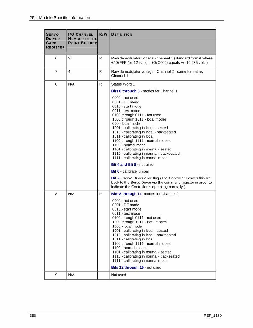
25.4 Module Specific Information
388 REF_1150
SE RVO DR I V E R CARD RE GI S T E R
I /O CH AN N E L NUM BE R I N TH E POI NT BUI L DE R
R/W DE FI NI T I O N
6 3 R Raw demodulator voltage - channel 1 (standard format where +/-0xFFF (bit 12 is sign, +0xC000) equals +/- 10.235 volts)
7 4 R Raw demodulator voltage - Channel 2 - same format as Channel 1
8 N/A R Status Word 1
Bits 0 through 3 - modes for Channel 1
0000 - not used 0001 - PE mode 0010 - start mode 0011 - test mode 0100 through 0111 - not used 1000 through 1011 - local modes 000 - local mode 1001 - calibrating in local - seated 1010 - calibrating in local - backseated 1011 - calibrating in local 1100 through 1111 - normal modes 1100 - normal mode 1101 - calibrating in normal - seated 1110 - calibrating in normal - backseated 1111 - calibrating in normal mode
Bit 4 and Bit 5 - not used
Bit 6 - calibrate jumper
Bit 7 - Servo Driver alive flag (The Controller echoes this bit back to the Servo Driver via the command register in order to indicate the Controller is operating normally.)
8 N/A R Bits 8 through 11- modes for Channel 2
0000 - not used 0001 - PE mode 0010 - start mode 0011 - test mode 0100 through 0111 - not used 1000 through 1011 - local modes 1000 - local mode 1001 - calibrating in local - seated 1010 - calibrating in local - backseated 1011 - calibrating in local 1100 through 1111 - normal modes 1100 - normal mode 1101 - calibrating in normal - seated 1110 - calibrating in normal - backseated 1111 - calibrating in normal mode
Bits 12 through 15 - not used
9 N/A Not used

25.4 Module Specific Information
REF_1150 389
SE RVO DR I V E R CARD RE GI S T E R
I /O CH AN N E L NUM BE R I N TH E POI NT BUI L DE R
R/W DE FI NI T I O N
A N/A
W Command Register
Bit 0 through 5 - not used
Bit 6 - Controller alive flag (blind copy of status word 1 bit 7)
Bits 7 through 15 - not used
B N/A Not used
C N/A Reserved
D N/A R/W Module Configuration Status Register (see page 399)
E N/A R Severe Errors Status Register (see page 401)
F N/A Electronic ID
25.4.7 SERVO DRIVER COMMANDS
Tuning Constant Commands
The following commands are used to set the values of important tuning constants. The syntax of each command is indicated and must be followed.
Tuning Constant Commands
COMM AND DE S C RI P TI O N
piGain = 9.20 PI Controller gain outside of deadband. This value is the higher of two gain values used in the position PI loop. This value is used when the valve is moving. When the valve is in a stable position, a lower value is used to avoid noise-induced control action.
piResetT = 1000
PI Controller reset time outside of deadband. Used in PI equation along with the gain value described previously. This value is one of two used in the PI equation. This one is used when the valve is in motion, and causes faster wind-up. It is given in milliseconds.
piGainDb = 1.40 PI Controller gain inside of deadband. When the valve is in a steady position, the PI gain is reduced to this value. This helps avoid noise-induced control action.
piResetTDb = 10000
PI Controller reset time inside of deadband. This is one of two values used, and causes slower control action. It is given in milliseconds.
retreatRate % per second rate of output retreat.
DIRECT =1 PI mode. In direct mode (DIRECT=1), the output goes in a direction with respect to target position. In indirect mode (DIRECT=0), the output goes negative when the target position moves negative with respect to position feedback.
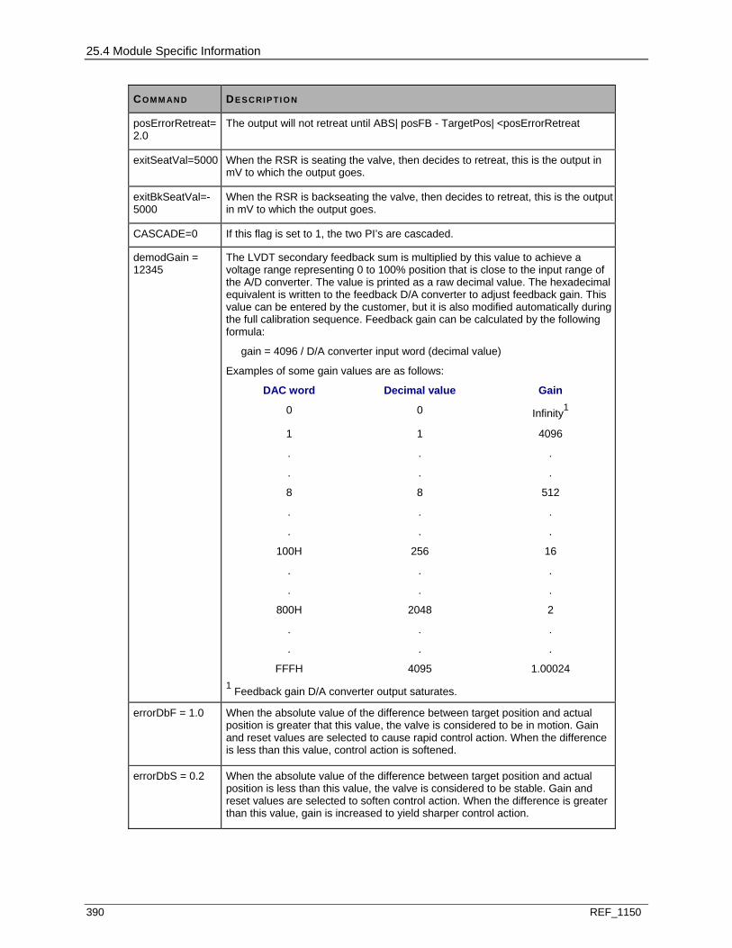
25.4 Module Specific Information
390 REF_1150
COMM AND DE S C RI P TI O N
posErrorRetreat=2.0
The output will not retreat until ABS| posFB - TargetPos| <posErrorRetreat
exitSeatVal=5000 When the RSR is seating the valve, then decides to retreat, this is the output in mV to which the output goes.
exitBkSeatVal=-5000
When the RSR is backseating the valve, then decides to retreat, this is the output in mV to which the output goes.
CASCADE=0 If this flag is set to 1, the two PI’s are cascaded.
demodGain = 12345
The LVDT secondary feedback sum is multiplied by this value to achieve a voltage range representing 0 to 100% position that is close to the input range of the A/D converter. The value is printed as a raw decimal value. The hexadecimal equivalent is written to the feedback D/A converter to adjust feedback gain. This value can be entered by the customer, but it is also modified automatically during the full calibration sequence. Feedback gain can be calculated by the following formula:
gain = 4096 / D/A converter input word (decimal value)
Examples of some gain values are as follows:
DAC word Decimal value Gain
0 0 Infinity1
1 1 4096
. . .
. . .
8 8 512
. . .
. . .
100H 256 16
. . .
. . .
800H 2048 2
. . .
. . .
FFFH 4095 1.00024 1 Feedback gain D/A converter output saturates.
errorDbF = 1.0
When the absolute value of the difference between target position and actual position is greater that this value, the valve is considered to be in motion. Gain and reset values are selected to cause rapid control action. When the difference is less than this value, control action is softened.
errorDbS = 0.2
When the absolute value of the difference between target position and actual position is less than this value, the valve is considered to be stable. Gain and reset values are selected to soften control action. When the difference is greater than this value, gain is increased to yield sharper control action.
25.4 Module Specific Information
REF_1150 391
COMM AND DE S C RI P TI O N
seatLimit = 0.0 When target valve position is equal to or less than this value, seating action controls the output.
backSeatLimit = 100.0
When the target valve position is equal to or greater than this value, backseating action controls the output.
contingency = 10.0
If the absolute value of the difference between Servo Driver target position and actual position is greater than this value, a contingency condition may exist. The condition must exist until a timer expires for it to be reported. The timer is described below:
A situation could arise where the Servo Driver target position and the Controller’s target are not equal. One example would be if the shutdown input were true, the Servo Driver set the target position to 0, but the Controller did not track. In this situation, contingency would not be reported if the valve went to 0% position.
contingencyTime = 10000
If the error between target position and actual position exceeds contingency for this amount of time, then the condition is reported to the Controller. This number is given in milliseconds.
calhndrd = 30000
This value is displayed in decimal. It is the converted hexadecimal A/D converter reading for the 100% position. It can be entered by the customer; however, it is normally determined automatically by the calibration sequence.
calzero = -30000
This value is displayed in decimal. It is the converted hexadecimal A/D converter reading for the 0% position. It can be entered by the customer; however, it is normally determined automatically by the calibration sequence.
Configuration Commands
COMM AND DE S C RI P TI O N
FIP = 1<return> Fail-in-place flag. If the fail-in-place flag is set, the valve will hold its last position when switching from normal mode to local mode. If the fail-in-place flag is clear (FIP = 0), the valve’s target position will be forced to -5% when switching from normal to local mode.
RDNDNT = 1<return>
Redundant LVDT option. If the redundant LVDT option is selected, the Servo Driver will execute only 1 PI control loop. However, it will continue to process both position feedback channels, middle-selects each to reject some noise, then high-selects between the two feedback values.
If the option is not selected (RDNDNT = 0), the Servo Driver behaves as a two-independent-channel closed loop servo control.
Note
This command has a different meaning for the Valve Positioner module.
PROP = 1<return>
Proportional output option. If the proportional output option is selected, the PI routine is not called. Instead, the position target in percent is copied directly to the output, in which case 0 to 100% demand would yield 0 to 10 volts at the output.
Normally the proportional output is not selected (PROP = 0), resulting in a closed loop PI control subsystem.
25.4 Module Specific Information
392 REF_1150
Miscellaneous Commands
COMM AND DE S C RI P TI O N
V1<return> Selects valve 1. The valve selected is indicated by the prompt character sequence. Subsequent commands affect only the selected channel.
V2<return> Selects valve 2. The valve selected is indicated by the prompt character sequence. Subsequent commands affect only the selected channel.
EXIT<return> Permits test and calibrate modes to be exited by executing a soft reset.
DG<return> Display group data - This function repeatedly displays important operating parameters such as demand, feedback, and feedback voltage.
HELP<return> Print command list

25.4 Module Specific Information
REF_1150 393
COMM AND DE S C RI P TI O N
diag<return> This command displays important status information in hexadecimal format. Included is the operating mode for each channel, SFE register, signal register, and restriction register as follows:
mod1=0xmm mod2=0xnn restricts=0xrrrrrrrr sgnls=0xssss sfe’s=0xeeee
where mm = Hex value for channel 1 mode:
0 through 5 are start modes 0x14 through 0x19 are local modes 0x28 through 0x2B are normal modes 0x3C through 0x3F are test modes
nn = Mode for channel 2
rrrrrrrr = Restriction bit set as follows:
bit 0 - PROM checksum error bit 1 - Memory diagnostic error bit 2 - Channel 1 contingency bit 3 - Channel 2 contingency bit 4 - Ovation serial bus not configured bit 5 - Mismatch of tuning constants between module and Controller bit 6 - Controller is not updating module bit 7 - Channel 1 - Controller is not tracking bit 8 - Channel 2 - Controller is not tracking bit 9 - EEPROM checksum error bit 10 - Hold until oscillator is stable bit 11 - Channel 1 - valve is under serial port control or calibrating bit 12 - Channel 2 - valve is under serial port control or calibrating
ssss = Signal bits as follows:
bit 10 - Channel 1 contingency bit 11 - Channel 2 contingency bit 12 - Display group is on bit 13 - Display group is turned on, display needs initialized
eeee = Severe fatal error bits as follows:
bit 0 - EEPROM checksum bit 1 - PROM checksum bit 2 - Shared memory readback error bit 3 - Processor memory readback error bit 4 - FPGA error on startup bit 5 - UART readback error bit 6 - Processor diagnostic error bit 7 - Not used bit 8 - PSD302 memory readback error
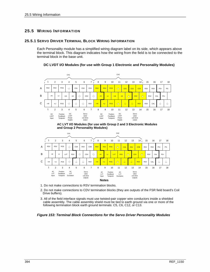
25.5 Wiring Information
394 REF_1150
25.5 WIRING INFORMATION
25.5.1 SERVO DRIVER TERMINAL BLOCK WIRING INFORMATION
Each Personality module has a simplified wiring diagram label on its side, which appears above the terminal block. This diagram indicates how the wiring from the field is to be connected to the terminal block in the base unit.
RSV RSV POS CD2 CD3
-LI-HI
CD1
-LI
+HI +LI POS
CDV-16
RSV
+16
+LI POS
-16
RSV
RSV
RSV
PS+ PS-
PS+
1 2 4 5
6 7 8 9 10 11 12 13 14 15 16 17 18
A
B
C
3 6 7 8 9 10 11 12 13 14 15 16 17 18
1 2 4 53
CDV+16
RSV
-HI
+HI CAL
CAL
RSVRSVCD1 CD2 CD3RSV POS
CH1 CH2
DCLVDTInput
PositionFeedbackTestpoint
DCLVDTPowerSupply
Servovalve
coil driveoutput
DCLVDTInput
PositionFeedbackTestpoint
DCLVDTPowerSupply
Servovalve
coil driveoutput
RSV RSV POS RSV CDB
-LI-HI
CDA
-LI
+HI +LI POS
CDVRSV
RSV
LVT
+LI POS
RSV
RSV
RSV
RSV
PS+ PS-
PS+
1 2 4 5
6 7 8 9 10 11 12 13 14 15 16 17 18
A
B
C
3 6 7 8 9 10 11 12 13 14 15 16 17 18
1 2 4 53
CDVLVT
RSV
-HI
+HI CAL
CAL
RSVRSVCDA RSV CDBRSV POS
CH1 CH2
ACLVTInput
PositionFeedbackTestpoint
ACLVT
Excitation
Servovalve
coil driveoutputs
ACLVTInput
PositionFeedbackTestpoint
ACLVT
Excitation
Servovalve
coil driveoutputs
Notes
3. All of the field interface signals must use twisted-pair copper wire conductors inside a shieldedcable assembly. The cable assembly shield must be tied to earth ground via one or more of thefollowing termination block earth ground terminals: C5, C6, C12, or C13.
1. Do not make connections to RSV termination blocks.2. Do not make connections to CDV termination blocks (they are outputs of the FSR field board's Coil
Drive buffers).
DC LVDT I/O Modules (for use with Group 1 Electronic and Personality Modules)
AC LVT I/O Modules (for use with Group 2 and 3 Electronic Modulesand Group 2 Personality Modules)
Figure 153: Terminal Block Connections for the Servo Driver Personality Modules

25.5 Wiring Information
REF_1150 395
Abbreviations Used in Diagrams
AB B R E V I AT I ON DE FI NI T I O N
Earth ground terminals.
Isolated circuit common ground.
+16, -16 DC LVDT Power Supply voltages, +16 VDC and -16 VDC.
CAL A jumper may be installed across the two CAL inputs in order to force the module to enter factory test mode.
CDA Primary 1000 ohm servo-valve coil drive output (AC LVT modules).
CDB Secondary 1000 ohm servo-valve coil drive output (AC LVT modules).
CDV Output of FSR field brand coil drive buffer (no connections allowed).
CD1 - CD3 CD1 = 60 ohm, 60 mA servo-valve coil drive output (DC LVDT modules).
CD2 = 80 ohm, 40 mA servo-valve coil drive output (DC LVDT modules).
CD3 = 40 ohm, 40 mA servo-valve coil drive output (DC LVDT modules).
+HI, -HI Position feedback inputs - high range (DC LVDTs only).
+LI, -LI Position feedback inputs - low range (DC LVDTs or AC LVTs).
LVT AC LVT primary winding sinusoidal excitation output.
POS Demodulated and amplified position feedback DC voltage (0.0 to 7.5 VDC)
PS+, PS- Auxiliary power supply terminals (not used).
RSV Reserved terminals. No connections allowed on these terminals.
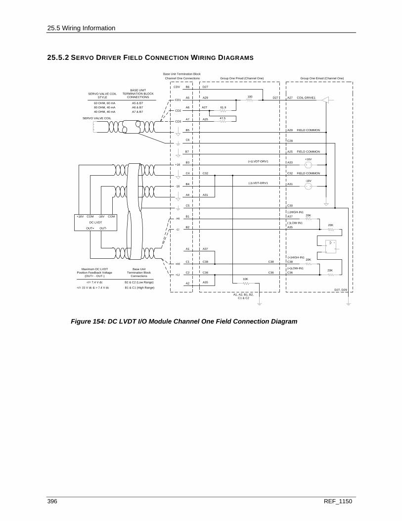
25.5 Wiring Information
396 REF_1150
25.5.2 SERVO DRIVER FIELD CONNECTION WIRING DIAGRAMS
COIL-DRIVE1A27D27
D27
A29A5
A25
100
61.9
47.5
B6
A27A6
A7
CDV
CD1
CD2
CD3
A29B5
C32
SERVO VALVE COIL
SERVO VALVE COILSTYLE
BASE UNITTERMINATION BLOCK
CONNECTIONS
60 OHM, 60 mA80 OHM, 40 mA40 OHM, 40 mA
A5 & B7A6 & B7A7 & B7
FIELD COMMON
C28
+16V
-16V
A33
A31
B3
C4
B4
C6
A31A4
+16
-16
C32 FIELD COMMON
C5
B7 A25 FIELD COMMON
A1 A37
C1 C38+HI
+LIC2 C36
A2 A35
B1-HI
B2-LI
C38
C30
C38
C36C36
A37
A35
DC LVDT
OUT-OUT+
+16V -16VCOM COM
0
0
0
0
(-)HIGH-IN1
(-)LOW-IN1
(+)LOW-IN1
(+)HIGH-IN1
Group One Emod (Channel One)
D27, D29
Group One Pmod (Channel One)Base Unit Termination Block
Maximum DC LVDTPosition Feedback Voltage
(OUT+ - OUT-)
Base UnitTermination Block
Connections
</= 7.4 V dc
</= 15 V dc & > 7.4 V dc
B2 & C2 (Low Range)
B1 & C1 (High Range)
20K
20K
20K
20K
Channel One Connections
(+)LVDT-DRV1
(-)LVDT-DRV1
10K
A1, A2, B1, B2,C1 & C2
Figure 154: DC LVDT I/O Module Channel One Field Connection Diagram

25.5 Wiring Information
REF_1150 397
COIL-DRIVE2A13D13
D13
A15A12
A11
100
61.9
47.5
B13
A13A13
A14
CDV
CD1
CD2
CD3
A15B12
C18
SERVO VALVE COIL
SERVO VALVE COILSTYLE
BASE UNITTERMINATION BLOCK
CONNECTIONS
60 OHM, 60 mA80 OHM, 40 mA40 OHM, 40 mA
A12 & B14A13 & B14A14 & B14
FIELD COMMON
C14
+16V
-16V
A19
A17
B10
C11
B11
C13
A17A11
+16
-16
C18 FIELD COMMON
C12
B14 A11 FIELD COMMON
A8 A23
C8 C24+HI
+LIC9 C22
A9 A21
B8-HI
B9-LI
C24
C16
C24
C22C22
A23
A21
DC LVDT
OUT-OUT+
+16V -16VCOM COM
0
0
0
0
(-)HIGH-IN2
(-)LOW-IN2
(+)LOW-IN2
(+)HIGH-IN2
Group One Emod (Channel Two)
D13, D15
Group One Pmod (Channel Two)Base Unit Termination Block
Maximum DC LVDTPosition Feedback Voltage
(OUT+ - OUT-)
Base UnitTermination Block
Connections
</= 7.4 V dc
</= 15 V dc & > 7.4 V dc
B9 & C9 (Low Range)
B8 & C8 (High Range)
20K
20K
20K
20K
Channel Two Connections
(+)LVDT-DRV2
(-)LVDT-DRV2
10K
A1, A2, B1, B2,C1 & C2
Figure 155: DC LVDT I/O Module Channel Two Field Connection Diagram

25.5 Wiring Information
398 REF_1150
COIL-DRIVE1A27D27
D27
A29A5
A25
200
200
B6
A7
CDV
CDA
CDB
A29
B7
C32
SERVO VALVE COILS(1000 OHM, 8 mA)
FIELD COMMON
C28
A33B3
C4
C6
LVT
C32 FIELD COMMON
C5
A1 A37
C1 C38+HI
+LIC2 C36
A2 A35
B1-HI
B2-LI
C38
C30
C38
C36C36
A37
A35
0
0
0
0
(-)HIGH-IN1
(-)LOW-IN1
(+)LOW-IN1
(+)HIGH-IN1
Group Two and Group Three Emod(Channel One)
D27, D29
Group Two Pmod (Channel One)Base Unit Termination Block
10K
10K
10K
10K
Channel One Connections
(+)LVDT-DRV1
B5
A25 FIELD COMMON
AC LVT
1 kHz (Group Two),3 kHz (Group Three)
10K
A1, A2, B1, B2,C1 & C2
Figure 156: AC LVT I/O Module Channel One Field Connection Diagram

25.6 Address Location Information
REF_1150 399
COIL-DRIVE2A13D13
D13
A15A12
A11
200
200
B13
A14
CDV
CDA
CDB
A15
B14
C18
SERVO VALVE COILS(1000 OHM, 8 mA)
FIELD COMMON
C14
A19B10
C11
C13
LVT
C18 FIELD COMMON
C12
A8 A23
C8 C24+HI
+LIC9 C22
A9 A21
B8-HI
B9-LI
C24
C16
C24
C22C22
A23
A21
0
0
0
0
(-)HIGH-IN2
(-)LOW-IN2
(+)LOW-IN2
(+)HIGH-IN2
Group Two and Group Three Emod(Channel Two)
D13, D15
Group Two Pmod (Channel Two)Base Unit Termination Block
10K
10K
10K
10K
Channel Two Connections
(+)LVDT-DRV1
B12
A11 FIELD COMMON
AC LVT
1 kHz (Group Two),3 kHz (Group Three)
10K
A1, A2, B1, B2,C1 & C2
Figure 157: AC LVT I/O Module Channel Two Field Connection Diagram
25.6 ADDRESS LOCATION INFORMATION
25.6.1 CONFIGURATION AND STATUS REGISTER
Word address 13 (D in Hex) is used to configure the module and provide status information to the Controller. The status register can be read by using the Point Information window at an Operator Station (see the Bit Pattern Field on the Hardware Tab). Refer to the applicable “Operator Station User Guide” for information about the Point Information window.

25.6 Address Location Information
400 REF_1150
Servo Driver Configuration/Status Register (Address 13 or D in Hex)
BI T DAT A DE S C R I P T I O N - CO NF I G U R AT I O N RE GI S T E R (WRI T E)
DAT A DE S C R I P T I O N - ST ATUS REGI S TER (RE AD)
0 Configure Module
(1 = configure)
Module is configured
(1 = configured; 0 = unconfigured)
1 Force Error
(1 = error; 0 = no error)
Internal or Forced Error
(1 = error; 0 = no error)
2 - 4 Communications Timeout Setting 1
BI T 4
BI T 3
BI T 2
T I M EO U T
0 0 0 16 seconds
0 0 1 4 seconds
0 1 0 2 seconds
0 1 1 1 seconds
1 0 0 500 milliseconds
1 0 1 250 milliseconds
1 1 0 125 milliseconds
1 1 1 62.5 milliseconds
Communications Timeout Setting 1
BI T 4
BI T 3
BI T 2
T I M EO U T
0 0 0 16 seconds
0 0 1 4 seconds
0 1 0 2 seconds
0 1 1 1 seconds
1 0 0 500 milliseconds
1 0 1 250 milliseconds
1 1 0 125 milliseconds
1 1 1 62.5 milliseconds 5 Not used Not used
6 Not used Not used
7 Severe fatal error (SFE) bit
Look at register E for more specific error information (error bits 0 through 6 in register E are OR’d to calculate this bit)
Severe fatal error (SFE) bit
Look at register E for more specific error information (error bits 0 through 6 in register E are OR’d to calculate this bit)
8 Not used Not used
9 Not used Ch1 - Retreat in progress
10 Not used Ch2 - Retreat in progress
11 Not used Ch1 - Retreat is disabled
12 Not used Ch2 - Retreat is disabled
13 Channel 1 contingency Channel 1 contingency
14 Channel 2 contingency Channel 2 contingency
15 EEPROM constants download request EEPROM constants download request
1 The tolerance on the timeout period is +/- 35%.

25.6 Address Location Information
REF_1150 401
25.6.2 SEVERE ERRORS STATUS REGISTER
Word address 14 (E in Hex) provides for additional module configuration and module status. The bit definitions for this register are encoded.
Severe Error Status Register (Address 14 or E in Hex)
BI T DAT A DE S C R I P T I O N - CO NF I G U R AT I O N RE GI S T E R (WRI T E)
DAT A DE S C R I P T I O N - ST ATUS RE GI S T E R (RE AD)
0 Not applicable EEPROM checksum error
1 Not applicable PROM checksum error
2 Not applicable Shared memory readback error
3 Not applicable Processor memory readback error
4 Not applicable FPGA error
5 Not applicable UART error
6 Not applicable Processor diagnostic error
7 Not used Not used
8 Not applicable PSD 302 memory readback error
9 Not used Not used
10 Not used Not used
11 File transfer bit - Reserved File transfer bit - Reserved
12 Controller-to-Servo Driver buffer control bit.
If Bit 12 and Bit 14 of register D are equal, then the buffer is not busy, and the Controller can write into the buffer.
If the two bits differ, then the Servo Driver should be in the process of unloading the buffer and will toggle Bit 14 when all data is removed.
The Controller should not write into the buffer if the two bits are unequal. When the Controller has data to be transferred to the Servo Driver, and the two bits are equal, it will first write the data, then toggle this bit. (The buffer occupies indirect registers 80 to BF inclusive. This buffer is accessed by the Controller using addresses 0 through 3F.)
Not applicable
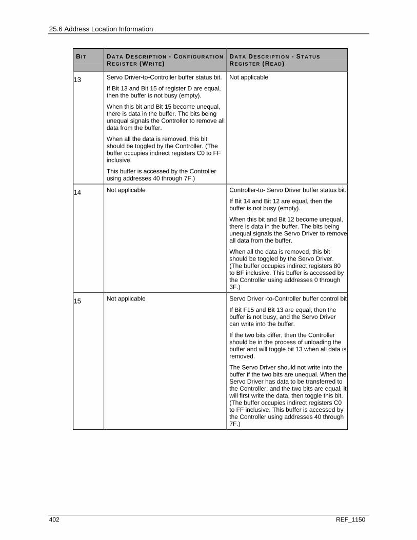
25.6 Address Location Information
402 REF_1150
BI T DAT A DE S C R I P T I O N - CO NF I G U R AT I O N RE GI S T E R (WRI T E)
DAT A DE S C R I P T I O N - ST ATUS RE GI S T E R (RE AD)
13 Servo Driver-to-Controller buffer status bit.
If Bit 13 and Bit 15 of register D are equal, then the buffer is not busy (empty).
When this bit and Bit 15 become unequal, there is data in the buffer. The bits being unequal signals the Controller to remove all data from the buffer.
When all the data is removed, this bit should be toggled by the Controller. (The buffer occupies indirect registers C0 to FF inclusive.
This buffer is accessed by the Controller using addresses 40 through 7F.)
Not applicable
14 Not applicable
Controller-to- Servo Driver buffer status bit.
If Bit 14 and Bit 12 are equal, then the buffer is not busy (empty).
When this bit and Bit 12 become unequal, there is data in the buffer. The bits being unequal signals the Servo Driver to remove all data from the buffer.
When all the data is removed, this bit should be toggled by the Servo Driver. (The buffer occupies indirect registers 80 to BF inclusive. This buffer is accessed by the Controller using addresses 0 through 3F.)
15 Not applicable
Servo Driver -to-Controller buffer control bit
If Bit F15 and Bit 13 are equal, then the buffer is not busy, and the Servo Driver can write into the buffer.
If the two bits differ, then the Controller should be in the process of unloading the buffer and will toggle bit 13 when all data is removed.
The Servo Driver should not write into the buffer if the two bits are unequal. When the Servo Driver has data to be transferred to the Controller, and the two bits are equal, it will first write the data, then toggle this bit. (The buffer occupies indirect registers C0 to FF inclusive. This buffer is accessed by the Controller using addresses 40 through 7F.)
25.7 Diagnostics
REF_1150 403
25.7 DIAGNOSTICS
The Servo Driver runs diagnostics to ensure that the circuit is operating properly. When a problem is detected, a number of things may occur. If the error is considered to be a severe fatal error, the card will “dive.” This means that the output circuit will de-power, and the on-board processor will “idle.” For some fatal errors, the processor will be reset. Word register E in the serial bus shared memory contains important severe fatal error bits.
Other problems may cause a restriction bit to be set. Restriction bits prevent the module from changing modes. During startup, each mode uses a bit mask to determine if errors exist that would prevent the mode change. As the mode advances from start, to local, then to normal, the restriction mask has fewer and fewer bits set.
During restart, there is a 20 second time delay to allow the oscillator to stabilize. Diagnostics are run during this delay. The EPROM checksum is fully calculated.
25.7.1 EPROM CHECKSUM ERROR
The EPROM checksum is calculated completely on restart. After restart, the checksum program is called during idle time. Each call to the checksum adds one word to the sum.
Memory Read/Write Check
A failure of any memory to read back correctly is considered a severe fatal error. The memory check routine accesses memory in the PSD302 chip, on-chip memory, and serial bus shared memory.
EEPROM Checksum
On restart, tuning constants are read out of a 64x16 EE memory. If the checksum calculation indicates an error, an SFE bit is set and all modes are restricted. This error occurs in the factory during manufacturing, but should never occur in the field.
UART Check
A byte is written to the UART scratchpad register and read back. If the data does not read back correctly, an SFE bit is set and all modes are restricted.
FPGA Error
During restart, the FPGA is loaded by the 80196 Controller. Control and status lines connected to the FPGA must conform to the defined sequence, otherwise an SFE bit is set and all modes are restricted.

25.8 Diagnostic LEDs
404 REF_1150
Controller Watchdog Timer
Microcontroller Firmware maintains a timer that is reset every time the Controller updates the Servo Driver with a new demand position. If the timer expires and the Servo Driver is in the normal operating mode, the module will revert back to the local operating mode.
The duration of the timer is set by three bits located in register D.
The microcontroller assumes an update has occurred when two conditions exist. First, it tests the CYCLEOK bit, which is an indication that a serial bus cycle to the module has occurred.
In addition to changing modes when the timer expires, a restriction bit is set to prevent return to normal mode. Updating demand will clear the restriction bit.
When the module switches to local mode, demand value is set to -5% if the “failInPlaceFlag” is cleared. If the “failInPlaceFlag” bit is set, demand value remains where it was when the mode change occurred.
25.8 DIAGNOSTIC LEDS
The following table lists the module’s LEDs and describes what they mean when lit.
Servo Driver Diagnostic LEDs
LED DE S C RI P TI O N
P (Green) Power OK LED. Lit when the +5V power is OK.
C (Green) Communications OK LED. Lit when the Controller is communicating with the module. Successful completion of sequence resets the watchdog timer.
E (Red) External Fault LED.
I (Red) Internal Fault LED. Possible causes:
Force Error bit (Bit 1) of the Configuration Register is set.
Also lit when a timeout of the watchdog timer occurs when Controller stops communicating with module.
1 - MODE (Green)
Channel 1
Lit whenever the module is operating in Normal mode.
Not lit whenever the module is operating in local manual mode.
1 - CONTINGCY (Red)
Channel 1
Lit to indicate Contingency Condition.
1 - BACKSEAT (Green)
Channel 1
Lit whenever seating or backseating is in effect.
1 - PI DETUNE (Green)
Channel 1
Lit whenever PI is detuned.
2 - MODE (Green)
Channel 2
Lit whenever the module is operating in Normal mode.
Not lit whenever the module is operating in local manual mode.
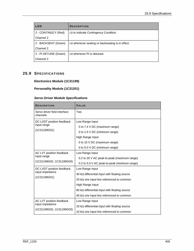
25.9 Specifications
REF_1150 405
LED DE S C RI P TI O N
2 - CONTINGCY (Red)
Channel 2
Lit to indicate Contingency Condition.
2 - BACKSEAT (Green)
Channel 2
Lit whenever seating or backseating is in effect.
2 - PI DETUNE (Green)
Channel 2
Lit whenever PI is detuned.
25.9 SPECIFICATIONS
Electronics Module (1C31199)
Personality Module (1C31201)
Servo Driver Module Specifications
DE S C RI P TI O N VALUE
Servo driver field interface channels
Two
DC LVDT position feedback input range
(1C31199G01)
Low Range Input
0 to 7.4 V DC (maximum range)
0 to 1.5 V DC (minimum range)
High Range Input
0 to 15 V DC (maximum range)
0 to 5.0 V DC (minimum range)
AC LVT position feedback input range
(1C31199G02, 1C31199G03)
Low Range Input
0.2 to 20 V AC peak-to-peak (maximum range)
0.2 to 5.0 V AC peak-to-peak (minimum range)
DC LVDT position feedback input impedance
(1C31199G01)
Low Range Input
40 kΩ differential input with floating source
20 kΩ one input line referenced to common
High Range Input
80 kΩ differential input with floating source
40 kΩ one input line referenced to common
AC LVT position feedback input impedance
(1C31199G02, 1C31199G03)
Low Range Input
20 kΩ differential input with floating source
10 kΩ one input line referenced to common
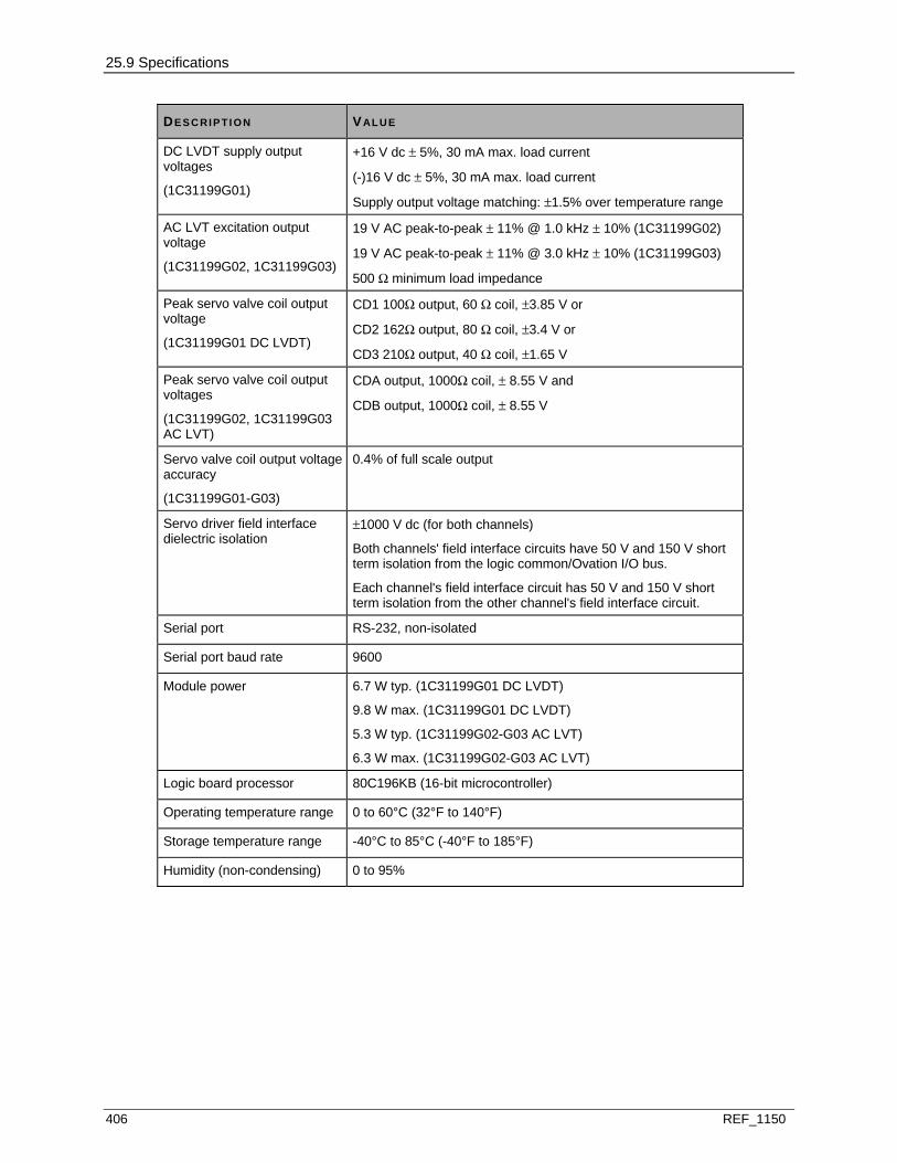
25.9 Specifications
406 REF_1150
DE S C RI P TI O N VALUE
DC LVDT supply output voltages
(1C31199G01)
+16 V dc ± 5%, 30 mA max. load current
(-)16 V dc ± 5%, 30 mA max. load current
Supply output voltage matching: ±1.5% over temperature range
AC LVT excitation output voltage
(1C31199G02, 1C31199G03)
19 V AC peak-to-peak ± 11% @ 1.0 kHz ± 10% (1C31199G02)
19 V AC peak-to-peak ± 11% @ 3.0 kHz ± 10% (1C31199G03)
500 Ω minimum load impedance
Peak servo valve coil output voltage
(1C31199G01 DC LVDT)
CD1 100Ω output, 60 Ω coil, ±3.85 V or
CD2 162Ω output, 80 Ω coil, ±3.4 V or
CD3 210Ω output, 40 Ω coil, ±1.65 V
Peak servo valve coil output voltages
(1C31199G02, 1C31199G03 AC LVT)
CDA output, 1000Ω coil, ± 8.55 V and
CDB output, 1000Ω coil, ± 8.55 V
Servo valve coil output voltage accuracy
(1C31199G01-G03)
0.4% of full scale output
Servo driver field interface dielectric isolation
±1000 V dc (for both channels)
Both channels' field interface circuits have 50 V and 150 V short term isolation from the logic common/Ovation I/O bus.
Each channel's field interface circuit has 50 V and 150 V short term isolation from the other channel's field interface circuit.
Serial port RS-232, non-isolated
Serial port baud rate 9600
Module power 6.7 W typ. (1C31199G01 DC LVDT)
9.8 W max. (1C31199G01 DC LVDT)
5.3 W typ. (1C31199G02-G03 AC LVT)
6.3 W max. (1C31199G02-G03 AC LVT)
Logic board processor 80C196KB (16-bit microcontroller)
Operating temperature range 0 to 60°C (32°F to 140°F)
Storage temperature range -40°C to 85°C (-40°F to 185°F)
Humidity (non-condensing) 0 to 95%
REF_1150 407
IN THIS SECTION
Description ......................................................................................................................408 Module Specific Information............................................................................................409 Wiring Information ...........................................................................................................413 Specifications ..................................................................................................................414
S E C T I O N 2 6
SLIM (SMALL LOOP INTERFACE MODULE)
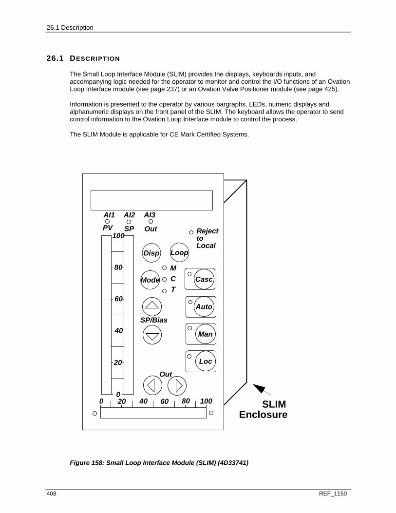
26.1 Description
408 REF_1150
26.1 DESCRIPTION
The Small Loop Interface Module (SLIM) provides the displays, keyboards inputs, and accompanying logic needed for the operator to monitor and control the I/O functions of an Ovation Loop Interface module (see page 237) or an Ovation Valve Positioner module (see page 425).
Information is presented to the operator by various bargraphs, LEDs, numeric displays and alphanumeric displays on the front panel of the SLIM. The keyboard allows the operator to send control information to the Ovation Loop Interface module to control the process.
The SLIM Module is applicable for CE Mark Certified Systems.
SLIM Enclosure
Disp
Auto
Man
Loc
SP/Bias
Out
0
20
40
60
80
100
0 20 40 60 80 100
RejecttoLocal
AI1
SP Out
CascMCT
Loop
Mode
AI2 AI3
PV
Figure 158: Small Loop Interface Module (SLIM) (4D33741)
26.2 Module Specific Information
REF_1150 409
26.2 MODULE SPECIFIC INFORMATION
26.2.1 FEATURES
Using keys on the front of the SLIM panel, the operator has the following capabilities:
Raise output. Lower output. Raise set point. Lower set point. Change SLIM mode (Group 1 only). Group 1 SLIMs operate in four modes: CONTROL, MONITOR, TUNING, LOOP. Group 2
operates in CONTROL mode only. Change alphanumeric and numeric displays. Change Loop Interface mode to Auto, Manual, Local (all groups) or Cascade (Group 1 only). Change tuning constants (Group 1 only). Runs bargraphs, LEDs, and alphanumeric and numeric displays to monitor Loop Interface I/O
activities. Scans keypad to control Loop Interface. Sends and receives information to and from the Loop Interface through a serial port. Flags a break in the communication link with the Ovation Loop Interface. Allows loop control even if the Ovation Controller is down. Displays:
Two 40-segment bargraph (for process variable and setpoint)
One 30-segment bargraph (for output)
One 4-digit numeric (for setpoint, output, process variable or analog input)
One 4-digit alphanumeric (for engineering units, status or SLIM mode information)
Thirteen status LEDs (for SLIM modes, Loop Interface modes as well as high and low limit conditions output)
Control keys: Four keys to raise and lower set point and outputs
Seven function keys
26.2.2 GROUPS AND MODES
The SLIM card is packaged in one of two possible assemblies. The keyboards are the same, except Group 2 does not have the LOOP, CASC, and MODE buttons.
Group 1 Allows the operator to choose from among four modes of operation for the SLIM and four for the Loop Interface.
Group 2 Offers no choice of modes for the SLIM; it always operates in the CONTROL mode. Offers three choices of operation of the Ovation Loop Interface.

26.2 Module Specific Information
410 REF_1150
The four modes of operation for the SLIM are as follows:
CONTROL MODE: Allows the operator to send control information to the Ovation Loop Interface through a keyboard; displays the process variable, the setpoint, and output value for the Ovation Loop Interface on a bargraph, and displays PV, SP, or OUT with proper engineering units on an alphanumeric display.
MONITOR MODE: (Group 1 only)
Displays the process variable, the set point, and output values for the Ovation Loop Interface on a bargraph and displays the analog input values on an alphanumeric display. Note that the Loop Interface does not contain an AI3 input.
TUNING MODE: (Group 1 only)
Displays the gain, reset, rate, and derivative gain values for the Ovation Loop Interface it is communicating with and enables the operator to change the values. Requires a password.
LOOP MODE: (Group 1 only)
Displays the Loop Number of the Loop Interface to which the SLIM is currently communicating.
Note
Only one Ovation Loop Interface may be connected to a SLIM.

26.2 Module Specific Information
REF_1150 411
Disp
Auto
Man
Loc
SP/Bias
Out
0
20
40
60
80
100
0 20 40 60 80 100
RejecttoLocal
PV SP Out
Disp
Auto
Man
Loc
SP/Bias
Out
0
20
40
60
80
100
0 20 40 60 80 100
RejecttoLocal
AI1
SP Out
CascMCT
Loop
Mode
AI2 AI3
PV
Figure 159: Keyboards for Group 1 and Group 2 SLIMs
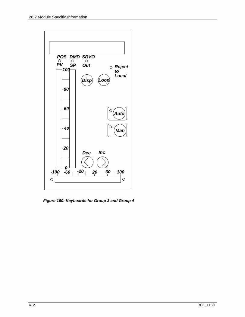
26.2 Module Specific Information
412 REF_1150
Auto
Man
Dec
0
20
40
60
80
100
-100 -60 -20 20 60 100
RejecttoLocal
POS
SP Out
Loop
DMD SRVO
PV
Inc
Disp
Figure 160: Keyboards for Group 3 and Group 4
26.3 Wiring Information
REF_1150 413
26.3 WIRING INFORMATION
26.3.1 WIRING
Power cables to the SLIM must be single stranded #16 AWG copper conductors with ring lugs on both ends. Power required at the terminal block of the SLIM is 0.5A at +12 VDC. No shielding is required. A backup power supply is optional.
+12A
+12B
RTN
RTN
SerialPort
Figure 161: Wiring
In installations with more than one SLIM, each SLIM should have its own pair of conductors directly from the power supply. If SLIMs are connected in parallel, conductors must be able to accommodate the total current requirement for all SLIMs; voltage must measure +12 VDC at the last SLIM in the line.
Serial Port
The Serial Port receives display and status data from the Loop Interface and also sends operator inputs from the keyboard to the Loop Interface. The port can communicate with only one Loop Interface.
26.4 Specifications
414 REF_1150
Serial Port Card-Edge Connector
COM PO NENT SI DE PI N DE S C RI P TI O N
1 Transmit +
2 Transmit -
3 Shield (Signal Ground)
4 Receive +
5 Receive -
6 through 10 Not Used
Assemblies
Cable assembly 5A26166 is used to connect the Ovation Loop Interface module to the SLIM in non-CE Mark certified systems.
Cable assembly 5A26429 is used to connect the Ovation Loop Interface module to the SLIM in CE Mark certified systems.
SLIM Power Supply Tray 4D33743Gxx is used to power the SLIM in non-CE Mark certified systems.
26.4 SPECIFICATIONS Current input
0.30 A typical @ 12 V +5%, -10% 0.50 A maximum
Isolation 500 VDC output to chassis ground
Humidity (non-condensing) 0 to 95%
REF_1150 415
IN THIS SECTION
Description ......................................................................................................................415 Module Group Information ..............................................................................................415 Wiring Information ...........................................................................................................417 Address Location Information .........................................................................................420 Diagnostic LEDs..............................................................................................................421 Specifications ..................................................................................................................422
27.1 DESCRIPTION
The Speed Detector Module determines the speed of a piece of equipment by measuring the frequency of the output signal from a tachometer. The tachometer output can be sinusoidal or a pulse train. The Speed Detector provides a 16-bit output at an update rate of 5 milliseconds for over-speed detection, and a 32-bit output at a variable update rate for speed regulation.
27.2 MODULE GROUP INFORMATION
27.2.1 ELECTRONICS MODULE (EMOD)
There is one Electronics module group for the Speed Detector Module:
1C31189G01
27.2.2 PERSONALITY MODULE (PMOD)
There is one Personality module group for the Speed Detector Module:
1C31192G01
S E C T I O N 2 7
SPEED DETECTOR MODULE

27.2 Module Group Information
416 REF_1150
27.2.3 SUBSYSTEMS, SPEED DETECTOR
Speed Detector Subsystems 1
RANG E CH AN N E L S EL E CT RO NI C MO D U LE
PE R S O N AL I T Y MODULE
16 bit speed (Low Res)
200 Hz min - 51200 Hz max
8 1C31189G01 1C31192G01
32 bit speed (High Res)
0.72 Hz min - 65535 Hz max
8 1C31189G01 1C31192G01
When using the Point Builder to define points for a Speed Detector module, only the following point types are valid for each channel:
I/O Name
Channel
1 High Resolution (speed value)
3 Low Resolution (speed value)
5 Open Wire
11 Latched Overspeed
12 Overspeed
13 Trip Relay Status
1 Trip Relay
2 Reset Calculations
Type
Input (can select I/O 1 or 3)
Input (can select I/O 1 or 3)
Input
Input
Input
Input
Output
Output
Terminal Block
Connection
In
In
Not applicable
Not applicable
Not applicable
Not applicable
Relay
Not applicable
1 This module will interface to ONE speed sensor to determine the rotation speed of a field device.
27.3 Wiring Information
REF_1150 417
27.3 WIRING INFORMATION
27.3.1 SPEED DETECTOR TERMINAL BLOCK WIRING INFORMATION
Each Personality module has a simplified wiring diagram label on its side, which appears above the terminal block. This diagram indicates how the wiring from the field is to be connected to the terminal block in the base unit.
Figure 162: Terminal Block Connections for the Speed Detector Personality Module
The following table lists and defines the abbreviations used in this diagram.
Abbreviations Used in Diagrams
AB B R E V I AT I ON DE FI NI T I O N
COM Common terminal of relay’s contact.
Earth ground terminals used to connect to input signal’s shield (see the figure below for field connections).
IN+, IN- Positive and negative terminal connections of input signal.
NC Normally closed terminal of relay’s contact.
NO Normally open terminal of relay’s contact.
SHD Shield (see page 418) of input signal’s cable.
All field signals leaving/entering the cabinet should be in shielded cables. The frequency input signal from the signal source must be in twisted-pair shielded cables. The shield must be grounded (see page 418).
Note: Do not use unmarked terminal block locations.

27.3 Wiring Information
418 REF_1150
27.3.2 SPEED DETECTOR FIELD CONNECTION WIRING DIAGRAMS
Figure 163: Passive Probe Field Connections for the Speed Detector PMod
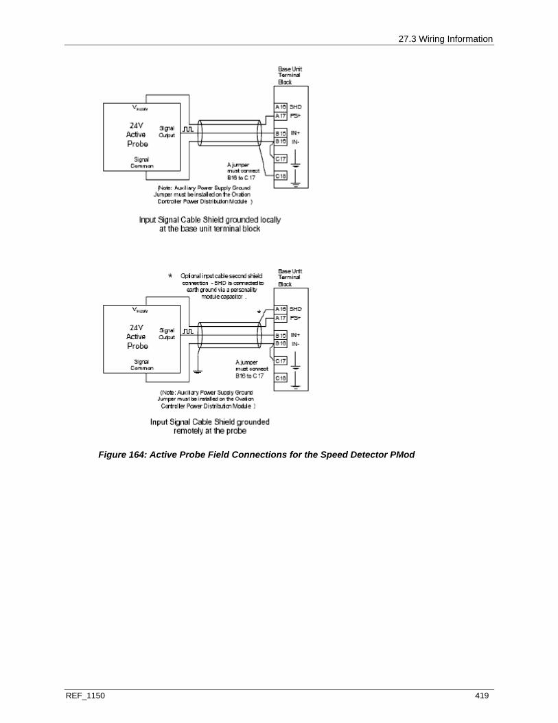
27.3 Wiring Information
REF_1150 419
Figure 164: Active Probe Field Connections for the Speed Detector PMod

27.4 Address Location Information
420 REF_1150
27.4 ADDRESS LOCATION INFORMATION
27.4.1 CONFIGURATION AND STATUS REGISTER
Word address 13 (D in Hex) is used to configure the module and provide status information to the Controller. The status register can be read by using the Point Information window at an Operator Station (see the Bit Pattern field on the Hardware tab). Refer to the applicable “Ovation Operator Station User Guide” for information about the Point Information window.
Speed Detector Configuration/Status Register (Address 13 or D in Hex)
Bit Data Description - Configuration Register (Write)
Data Description - Status Register (Read)
0 Configure Module
(1 = configure; 0 = unconfigure, causing a stoppage of both output measurements)
Module Configured
(1 = configured; 0 = unconfigured causing a stoppage of both output measurements)
1 Force Internal Error
(1 = force an attention status to be read by Controller; 0 = no forced error)
Forced Internal error
(1 = forced error set by Controller;
0 = no forced error)
2 Not used Not used
3 Not used Not used
4 Not used Bit 4 = 1, Open wire condition detected.
5 1 = enable open wire test Bit 5 = 1, Open wire test enabled.
6 Not used Not used
7 Not used Not used
8 Not used Not used
9 Not used Not used
10 Not used Bit 10 = 1, currently in overspeed condition.
11 Not used Bit 11 = 1, an overspeed condition detected since last read of register D. Reading register D will clear this bit.
12 Not used Bit 12 = 0, relay open.
Bit 12 = 1, relay energized.
13 Not used Not used.
14 Relay control 1 Relay control 0
15 Relay control 2 Relay control 1

27.4 Address Location Information
REF_1150 421
Secondary Configuration and Status Register
Word address 14 (E in Hex) provides the Pulse Count per update setting.
Overspeed Register
Word address 12 (C in Hex) provides the Overspeed Condition setting.
How to Specify the Pulse Count Per Update Setting
Determine the update period of the 32-Bit speed output. Normally, this is used to control the speed of equipment where accuracy is important. A longer update period will permit an higher accuracy output. Therefore, the maximum update period allowed by the control loop should be used to update the Speed Detector module’s 32-Bit speed output.
Example: The Ovation control system runs at a 50 millisecond loop time. The equipment operates at 10,000 Hz. The largest Pulse Count per Update setting that should be written to register 0EH = 10,000 Hz x 0.050 seconds) = 500
Another factor that should be considered is the number of teeth in the speed sensor’s gear. The Speed Detector module provides the speed sensor output signal frequency. The Ovation control system regulates equipment speed in revolutions per minute (rpm) using the measured Speed Detector module speed sensor output frequency (Hz) as follows:
Equipment speed (rpm) = 60 x frequency (Hz) / number of teeth in the gear.
To eliminate errors due to mechanical differences of teeth in the gear, complete revolutions of the speed sensor’s gear must be counted when measuring frequency. To implement this requirement, the Pulse Count per Update setting written to Speed Detector module register 0EH should be specified as an integer multiple of the speed sensor gear teeth quantity.
Example: There are 60 teeth in the speed sensor’s gear. With a 50 millisecond loop time and with the equipment operating at 10,000 Hz, the largest speed Speed Detector module Pulse Count per Update setting (written to register 0EH) is 500. The largest integer multiple of 60 teeth that is less than the maximum pulse count per update setting of 500 is 8. Therefore, a Pulse Count per Update value of 8 x 60 = 480 should be written to register 0EH as the Pulse Count per Update. The Pulse Count per Update is set to 480 in order to be a multiple of the number of teeth in the gear. The Pulse Count per Update setting of 480 provides an update every (480/10,000 = 48 milliseconds) which is fast enough for a 50 millisecond control loop.
For this example, a value of 01EOH (480) should be written to the Speed Detector.
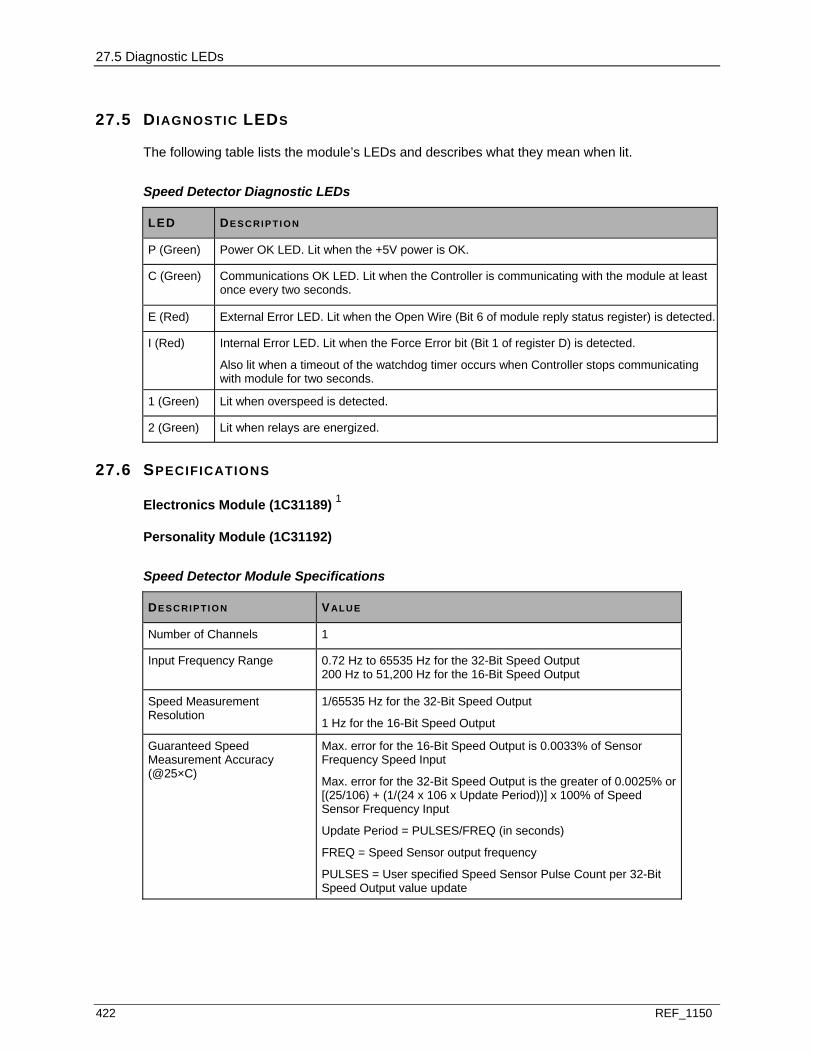
27.5 Diagnostic LEDs
422 REF_1150
27.5 DIAGNOSTIC LEDS
The following table lists the module’s LEDs and describes what they mean when lit.
Speed Detector Diagnostic LEDs
LED DE S C RI P TI O N
P (Green) Power OK LED. Lit when the +5V power is OK.
C (Green) Communications OK LED. Lit when the Controller is communicating with the module at least once every two seconds.
E (Red) External Error LED. Lit when the Open Wire (Bit 6 of module reply status register) is detected.
I (Red) Internal Error LED. Lit when the Force Error bit (Bit 1 of register D) is detected.
Also lit when a timeout of the watchdog timer occurs when Controller stops communicating with module for two seconds.
1 (Green) Lit when overspeed is detected.
2 (Green) Lit when relays are energized.
27.6 SPECIFICATIONS
Electronics Module (1C31189) 1
Personality Module (1C31192)
Speed Detector Module Specifications
DE S C RI P TI O N VALUE
Number of Channels 1
Input Frequency Range 0.72 Hz to 65535 Hz for the 32-Bit Speed Output 200 Hz to 51,200 Hz for the 16-Bit Speed Output
Speed Measurement Resolution
1/65535 Hz for the 32-Bit Speed Output
1 Hz for the 16-Bit Speed Output
Guaranteed Speed Measurement Accuracy (@25×C)
Max. error for the 16-Bit Speed Output is 0.0033% of Sensor Frequency Speed Input
Max. error for the 32-Bit Speed Output is the greater of 0.0025% or [(25/106) + (1/(24 x 106 x Update Period))] x 100% of Speed Sensor Frequency Input
Update Period = PULSES/FREQ (in seconds)
FREQ = Speed Sensor output frequency
PULSES = User specified Speed Sensor Pulse Count per 32-Bit Speed Output value update
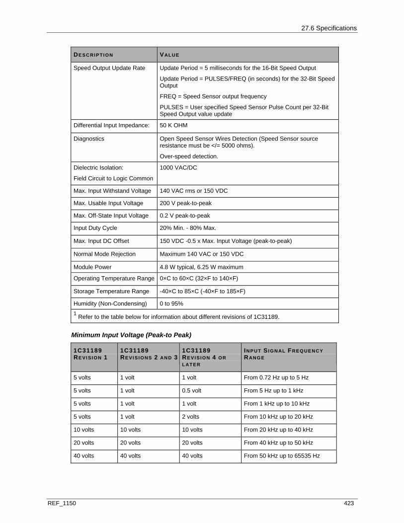
27.6 Specifications
REF_1150 423
DE S C RI P TI O N VALUE
Speed Output Update Rate Update Period = 5 milliseconds for the 16-Bit Speed Output
Update Period = PULSES/FREQ (in seconds) for the 32-Bit Speed Output
FREQ = Speed Sensor output frequency
PULSES = User specified Speed Sensor Pulse Count per 32-Bit Speed Output value update
Differential Input Impedance: 50 K OHM
Diagnostics Open Speed Sensor Wires Detection (Speed Sensor source resistance must be </= 5000 ohms).
Over-speed detection.
Dielectric Isolation:
Field Circuit to Logic Common
1000 VAC/DC
Max. Input Withstand Voltage 140 VAC rms or 150 VDC
Max. Usable Input Voltage 200 V peak-to-peak
Max. Off-State Input Voltage 0.2 V peak-to-peak
Input Duty Cycle 20% Min. - 80% Max.
Max. Input DC Offset 150 VDC -0.5 x Max. Input Voltage (peak-to-peak)
Normal Mode Rejection Maximum 140 VAC or 150 VDC
Module Power 4.8 W typical, 6.25 W maximum
Operating Temperature Range 0×C to 60×C (32×F to 140×F)
Storage Temperature Range -40×C to 85×C (-40×F to 185×F)
Humidity (Non-Condensing) 0 to 95% 1 Refer to the table below for information about different revisions of 1C31189.
Minimum Input Voltage (Peak-to Peak)
1C31189 RE VI S I O N 1
1C31189 RE VI S I O NS 2 AN D 3
1C31189 RE VI S I O N 4 OR L ATE R
IN P U T SI G N AL FR EQ UE N CY RANG E
5 volts 1 volt 1 volt From 0.72 Hz up to 5 Hz
5 volts 1 volt 0.5 volt From 5 Hz up to 1 kHz
5 volts 1 volt 1 volt From 1 kHz up to 10 kHz
5 volts 1 volt 2 volts From 10 kHz up to 20 kHz
10 volts 10 volts 10 volts From 20 kHz up to 40 kHz
20 volts 20 volts 20 volts From 40 kHz up to 50 kHz
40 volts 40 volts 40 volts From 50 kHz up to 65535 Hz


REF_1150 425
IN THIS SECTION
Descriptions.....................................................................................................................426 Module Group Information ..............................................................................................429 Module Specific Information............................................................................................432 Calibration .......................................................................................................................451 Wiring Information ...........................................................................................................460 SLIM Serial Port Connector ............................................................................................469 Address Location Information .........................................................................................470 Diagnostics......................................................................................................................472 Troubleshooting ..............................................................................................................474 Diagnostic LEDs..............................................................................................................477 Specifications ..................................................................................................................478
S E C T I O N 2 8
VALVE POSITIONER MODULE
28.1 Descriptions
426 REF_1150
28.1 DESCRIPTIONS
28.1.1 DESCRIPTION FOR SINGLE VP MODULE
The Digital Electro-Hydraulic (DEH) system controls steam turbine valve positions in order to adjust steam flow for turbine speed control, or to change generator load when connected to the grid. The Ovation Valve Positioner I/O module provides an interface between the DEH Ovation Controller and an electro-hydraulic servo valve actuator. Valve styles controlled by the Ovation Valve Positioner I/O module include throttle valves, governor valves, interceptor valves, extraction valves, and bypass valves. The Ovation Valve Positioner module provides closed-loop valve positioning control.
A valve position set point is maintained by the module. The set point is normally altered by the Ovation Controller via the Ovation I/O bus. If the Ovation Valve Positioner module operates in Local Manual mode, the set point is controlled by a SLIM operator interface station. Inside the electronics module, an 80C196 microcontroller provides real-time closed loop proportional-plus-integral (PI) control.
The Ovation Valve Positioner I/O module generates redundant output control signals which drive the electro-hydraulic servo valve actuator coils. The feedback loop is closed with the valve’s position measurement being obtained from a Linear Variable Differential Transformer (LVDT) that is mounted on the valve stem.
The Valve Positioner module can perform the following:
Calibration Diagnostics 10 millisecond loop time SLIM interface for local control Local serial interface for testing and calibration Shutdown input Seating and backseating logic
The Valve Positioner Module is applicable for CE Mark Certified Systems.
28.1 Descriptions
REF_1150 427
Description and Guidelines for Redundant VP Module
Two Ovation Valve Positioner (VP) cards operate as a Primary/Backup pair to control a single steam valve. The steam valve is fitted with two LVDTs, one connected to each Valve Positioner. Each VP then drives one coil in a high pressure hydraulic servo valve. The coils are completely isolated.
The Valve Positioners communicate serially to determine which VP should be Primary, and which should be Backup. Critical parameters of the redundant subsystem are exchanged over the serial link. These critical parameters are also exchanged over the Ovation bus, thus providing a redundant data path.
The Backup VP suspends its software PI routine, and replicates the servo output of the Primary. It then takes over control if the Primary fails. There are three types of failures that the subsystem will detect and respond to:
Hardware Failures - Each VP continuously runs internal diagnostics and will cease operations if a diagnostic fails. A failure is indicated when both the serial communications and Ovation line watchdog timers expire. The VP card continuously executes these diagnostics:
Microcontroller RAM
Ovation RAM
EPROM Checksum
DA Converter Readback
Ovation Watchdog Timer
Redundant Communications Watchdog Timer
28.1 Descriptions
428 REF_1150
Coil Drive - If the Primary VP detects a shorted or open servo coil, it will transfer control to the Backup VP. There is a customer setup requirement described in the section on servo coil failures.
LVDT Failures - LVDT failures are detected by measuring the derivative of position feedback. As with the servo coil, there are setup requirements that enable the detection of LVDT problems. The requirements are described in the section on LVDT failures.
The VP pair utilizes the SLIM serial port for VP-to VP communications. The serial link is a VP-to-VP connection, not the “party-line” bus utilized with the SLIM.
Failover events are NOT bumpless (that is, the valve will dip, or move in the direction indicated by the mechanical bias setting, during the failover period). Catastrophic hardware failures, or removal of the Primary VP, are the worst failures because the Backup must wait for various timers to expire and then engage the PI loop.
If, for example, the failover required one second to complete (determined by the Controller loop time for example), and the valve was programmed to drift shut in 30 seconds under control of the mechanical bias-setting, the valve could drift 3% (=1/30).
VP
VP
SLIM Serial Port
LVDT
1
Servo Valve
Coil 1 Coil 2
ACTUATOR
OvationBus
LVDT
2
Figure 165: Redundant Ovation Valve Positioner Subsystem

28.2 Module Group Information
REF_1150 429
VP-to VP Serial Connection
Figure 166: Redundant VP to VP Serial Connections
28.2 MODULE GROUP INFORMATION
28.2.1 ELECTRONIC MODULES (EMODS)
There are two Electronics module groups for the Valve Positioner module:
1C31194G01 provides 17 Volts AC peak-to-peak 1 KHz LVDT drive. 1C31194G02 provides 23.75 Volts AC peak-to-peak 3 KHz LVDT drive.
Note: When using the I/O Builder to configure the Valve Positioner (VP) module, note that whatever voltage/current description is displayed in the Slot position at the top of the window does NOT impact the configuration of the VP module.
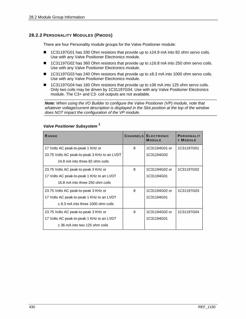
28.2 Module Group Information
430 REF_1150
28.2.2 PERSONALITY MODULES (PMODS)
There are four Personality module groups for the Valve Positioner module:
1C31197G01 has 330 Ohm resistors that provide up to ±24.9 mA into 82 ohm servo coils. Use with any Valve Positioner Electronics module.
1C31197G02 has 360 Ohm resistors that provide up to ±16.8 mA into 250 ohm servo coils. Use with any Valve Positioner Electronics module.
1C31197G03 has 240 Ohm resistors that provide up to ±8.3 mA into 1000 ohm servo coils. Use with any Valve Positioner Electronics module.
1C31197G04 has 160 Ohm resistors that provide up to ±36 mA into 125 ohm servo coils. Only two coils may be driven by 1C31197G04. Use with any Valve Positioner Electronics module. The C3+ and C3- coil outputs are not available.
Note: When using the I/O Builder to configure the Valve Positioner (VP) module, note that whatever voltage/current description is displayed in the Slot position at the top of the window does NOT impact the configuration of the VP module.
Valve Positioner Subsystem 1
RANG E CH AN N E L S EL E CT RO NI C MO D U LE
PE R SO N AL I TY MODULE
17 Volts AC peak-to-peak 1 KHz or
23.75 Volts AC peak-to-peak 3 KHz to an LVDT
24.8 mA into three 82 ohm coils
8 1C31194G01 or
1C31194G02
1C31197G01
23.75 Volts AC peak-to-peak 3 KHz or
17 Volts AC peak-to-peak 1 KHz to an LVDT
16.8 mA into three 250 ohm coils
8 1C31194G02 or
1C31194G01
1C31197G02
23.75 Volts AC peak-to-peak 3 KHz or
17 Volts AC peak-to-peak 1 KHz to an LVDT
± 8.3 mA into three 1000 ohm coils
8 1C31194G02 or
1C31194G01
1C31197G03
23.75 Volts AC peak-to-peak 3 KHz or
17 Volts AC peak-to-peak 1 KHz to an LVDT
± 36 mA into two 125 ohm coils
8 1C31194G02 or
1C31194G01
1C31197G04

28.2 Module Group Information
REF_1150 431
RANG E CH AN N E L S EL E CT RO NI C MO D U LE
PE R SO N AL I TY MODULE
When using the Point Builder to define points for a Valve Positioner module, only the following point types are valid for each channel:
I/O Channel
Name Type Input Source or Output Destination
Terminal Block Connection 2
1 Shutdown Status Input Valve Positioner DI1
2 Auxiliary (wetting) Voltage Sense Input Valve Positioner DI2
3 SLIM ON Signal Input Valve Positioner DI3
4 Position Feedback Input Valve Positioner
5 Coil 1 Voltage (Read-back)
Input Valve Positioner Coil 1
6 Coil 2 Voltage (Read-back)
Input Valve Positioner Coil 2
7 Coil 3 Voltage (Read-back)
Input Valve Positioner Coil 3
8 Raw Demodulator Voltage Input Valve Positioner
9 VP Status Input Valve Positioner
10 Demand Feedback Input Valve Positioner
11 VP Command Output Valve Positioner
12 VP Demand Output Valve Positioner
13 Partner Position Feedback Output Valve Positioner 1 This module will provide an interface between an Ovation Controller and ONE Electro-Hydraulic (EH) servo-valve actuator in the field. To use this module, the MASTATION algorithm must reside in the Ovation Controller. (See the Algorithm Reference Manual.) 2 The terminal block connection depends upon the application being used. Refer to wiring diagrams.
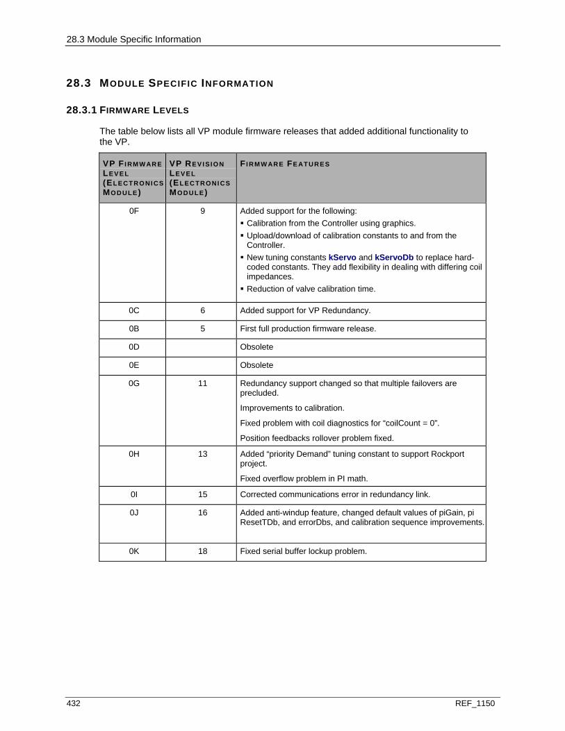
28.3 Module Specific Information
432 REF_1150
28.3 MODULE SPECIFIC INFORMATION
28.3.1 FIRMWARE LEVELS
The table below lists all VP module firmware releases that added additional functionality to the VP.
VP FI RM WAR E LEV E L (EL E C TR O NI CS MO D U LE)
VP REV I S I O N LEV E L (EL E C TR O NI CS MO D U LE)
F I RM W ARE FE AT U R E S
0F 9 Added support for the following: Calibration from the Controller using graphics. Upload/download of calibration constants to and from the Controller.
New tuning constants kServo and kServoDb to replace hard-coded constants. They add flexibility in dealing with differing coil impedances.
Reduction of valve calibration time.
0C 6 Added support for VP Redundancy.
0B 5 First full production firmware release.
0D Obsolete
0E Obsolete
0G 11 Redundancy support changed so that multiple failovers are precluded.
Improvements to calibration.
Fixed problem with coil diagnostics for “coilCount = 0”.
Position feedbacks rollover problem fixed.
0H 13 Added “priority Demand” tuning constant to support Rockport project.
Fixed overflow problem in PI math.
0I 15 Corrected communications error in redundancy link.
0J 16 Added anti-windup feature, changed default values of piGain, pi ResetTDb, and errorDbs, and calibration sequence improvements.
0K 18 Fixed serial buffer lockup problem.
28.3 Module Specific Information
REF_1150 433
28.3.2 PRIMARY/BACKUP STATUS TRANSITIONS
Primary to Backup
If the VP is in the Primary mode, it will transition to Backup mode if:
Serial Line Status is OK and Ovation Watchdog bit indicates partner is Alive, and is the primary (start condition).
Partner is OK according to serial line data. Partner is OK according to Ovation data. Its own status is not OK.
Backup to Primary
If the VP is in the Backup mode, it will transition to Primary mode if:
Its own status is OK and the partner’s Ovation Watchdog Bit indicates Not Alive and Serial Line Status is not OK.
Partner is in Backup mode, according to serial data. Partner is in Backup mode, according to Ovation data.
Setup Requirements
The following items must be set up before operating redundant Ovation Valve Positioner modules:
LVDT Setup
There are requirements on the LVDT setup for a redundant subsystem.
First, the linear range of the LVDT must exceed the mechanical range. This means that when the valve is at either endpoint, one of the secondary voltages will be at its minimum. The secondary voltage must be large enough at the endpoint so that if a wire breaks and the secondary voltage goes to zero, the change of voltage will be large enough to be readily detected. A good guideline is to ensure that each secondary always contributes at least 10%, positive or negative, to the demodulated voltage. That is,
min (|A|, |B|) / (|A| + |B|) > 10%
This minimum secondary value is expressed in percentage, is tunable, and is called MIN2NDRY.
Second, the LVDTs must be calibrated prior to being placed into redundant service, and for all possible positions, the feedback signal of the Primary should be near the feedback signal of the backup. This value is called LVDTTRACKING, and its default value is 1%.
28.3 Module Specific Information
434 REF_1150
Coil Setup
Coil diagnostics rely on a steady voltage across the coil. This voltage will be present if you adjust the servo valve per the Emerson recommendation.
The servo valve has a mechanical bias set-screw that pushes the spool to one side, allowing fluid to escape the actuator and slowly close the valve in the absence of electrical excitation. In the standard setup approximately 200 mV across both coils opposes the mechanical bias adjustment and holds the spool in the center position, trapping the fluid in the actuator, and holding the valve in a fixed position. Adjusting coil current changes spool position so that current can flow into or escape from the actuator. (Technically, the operation of the servo valve is dependent on current through the coil and the mechanical bias adjustment. However, the VP is set up to measure voltage across the coil and at the amplifier output, so voltage measurements are typically referenced in this description.)
28.3.3 VALVE POSITIONER MODES
Rapid or erratic valve movement can damage the turbine. The Valve Positioner enforces a set of rules to accomplish bumpless transfer between modes. The description of each mode includes mode transfer.

28.3 Module Specific Information
REF_1150 435
Start Mode
When the Valve Positioner is powered-up or restarted, its primary objective is to avoid an indeterminate output that would result in valve movement, and possible damage to the valve or turbine. There are a number of hardware and software features that prevent an indeterminate output.
The hardware is designed so that when the Valve Positioner is powered-up, the power supply to the servo output is turned off. With no current flow to the servo valve, it is left under the influence of its mechanical bias adjustment, the assumed state prior to power-up. In addition, the coil drive D/A convertor is not turned on until it receives the first output pattern.
As part of the microcontroller’s start sequence, the power supply is turned on, and then a pattern is written to the coil drive D/A convertor representing 0 volts. The result is that the servo output is under software control, no current flows between the Valve Positioner and the servo valve, and no valve movement has occurred.
The Valve Positioner will not remain in Start mode unless a diagnostic error is detected. The Valve Positioner transitions from Start to Local mode if all of the following functions execute and return “normal” or “ok” status codes:
Program the FPGA. Go to Factory Configure Mode if PE pin is 1. Check PE pin. Go to Factory Test Mode, if required. EPROM checksum check. EEPROM checksum check. RAM read/write test. D/A convertor readback diagnostic. UART scratchpad read/write test. Shared memory readback check.
The Valve Positioner will set target valve demand equal to demand feedback before transferring to Local mode.

28.3 Module Specific Information
436 REF_1150
Local-Manual Mode
The purpose of local-manual mode is:
Maintain stable valve position when the Controller fails or is reset. Smooth operation using manual raise/lower function. Bumpless transfer to normal mode. (Tracking by the Controller is required, and is enforced by
the Valve Positioner in local-manual mode.)
In local-manual mode, the Valve Positioner controls the valve using a set point that is only changed through the SLIM interface, or through the local serial interface.
Local-manual mode will be entered from normal mode if the Controller fails or stops updating the Valve Positioner card. When the Valve Positioner is powered up, local-manual mode is always entered as long as there are no diagnostic failures.
The preferred mode of Valve Positioner operation is normal mode. The Valve Positioner transfers from local-manual to normal if the following conditions are met: (1) Controller is updating the set point, thus keeping the watchdog timer from expiring. (2) Controller is tracking.
In local-manual mode, the following functions are performed:
PI position control loop. Writes current valve position to Ovation memory. Writes coil voltages to Ovation memory. Open coil diagnostic. Shorted coil diagnostic. EPROM checksum diagnostic. RAM diagnostic. Watchdog timing. SLIM interface (Raise, Lower, and update SLIM values.) Valve contingency diagnostic.

28.3 Module Specific Information
REF_1150 437
Normal Mode
Normal is the preferred mode of the Valve Positioner card. In normal mode, the Valve Positioner is receiving a position set point from the Controller and controlling valve position.
In normal mode, the following functions are performed:
PI position control loop (Demand position comes from the Controller via the Ovation memory). Writes current valve position to Ovation I/O memory. Writes coil voltages to Ovation I/O memory. Open coil diagnostic. Shorted coil diagnostic. EPROM checksum diagnostic. RAM diagnostic. Watchdog timing. SLIM interface (Updates SLIM values, no raise/lower function.) Valve contingency diagnostic.
Calibrate Mode
Calibrate mode is a submode of local-manual mode. Calibration sequences are commanded through the local serial port.
The Valve Positioner is commanded to calibrate when the appropriate bit in the command word is set. This causes the Valve Positioner to enter the calibrate mode and begin its travel sequence. During the travel sequence, the Valve Positioner will report a position feedback calculated using the most recent calibration numbers. The controlling MASTATION will enter manual mode and track the position demand feedback. The Valve Positioner moves the valve at a programmable rate during the travel sequence.
The Valve Positioner can exit calibrate mode without enforcing a bumpless transfer rule.
The following calibrate sequences are supported:
Zero Hot Cal This calibration sequence is executed to re-establish the 0% position. It is useful after the valve has been fully calibrated and the mechanical assembly has been heated and expanded. It avoids fully opening the valve.
Feedback gain is not adjusted during the hot cal sequence. Top Hot Cal
This calibration sequence is executed to re-establish the 100% position. It is useful after the valve has been fully calibrated and the mechanical assembly has been heated and expanded. It avoids fully closing the valve.
Feedback gain is not adjusted during the hot cal sequence. Null-Point Cal
This calibration sequence causes the valve to travel to the electrical null point of the LVDT. Null point calibration can be requested at the same time as full calibration, in which case the movement sequence is the full calibration sequence. However, the valve stops at the null point when it is encountered.
28.3 Module Specific Information
438 REF_1150
Full Calibration This calibration sequence is executed to re-establish 0% position, 100% position, and feedback gain.
When full calibration is requested the module enters local mode, requiring the Controller to track. The module then moves the value to the 0% position. The firmware checks for position feedback between the arbitrary limits of –9.7 volts and –2.0 volts. If the voltage is less (more negative) than –9.7 volts, the firmware reduces gain to make the voltage more positive than –9.7. If the voltage is more positive than –2.0 volts, the gain is increased until the voltage is more negative than –2.0 volts. During these two sequences, the gain is tested to insure it does not go out of allowable range.
If the voltage is between –9.7 and –2.0, then gain is recalculated to set the voltage to the arbitrary target voltage of –0.35 volts, and the firmware sequence advances to the next state, which will take the value to 100%.
At this point in the sequence, the demodulator gain has been set to a value that is a maximum allowable value. The gain may be reduced at the other end of the stroke, but will not be increased.
Now the valve moves to the 100% position. The feedback voltage is examined, and if it exceeds 10.0 volts, feedback gain is reduced. Once feedback voltage is less than +10.0 volts, it is recorded as the 100% calibration value.
The valve moves back to 0% and the voltage at 0% is recorded. Feedback gain is not adjusted.
The last step is to write 0% position, 100% position, and feedback gain to the EE memory.
Once the data is recorded in EE memory, the firmware clears a restriction flag, allowing the module to transfer from local mode back to normal mode. At this point the valve is under the control of the MA station and will return to the previous position according to the tuning of the MA.
28.3.4 CONTROLLER INTERFACE
This section defines direct-access Ovation shared memory registers from the Controller point of view. The Controller point-of-view is at the internal workings of the algorithm (the MASTATION is assumed). Conversions may occur between the applications level and the level described here. This format is used for start up, local, and normal operating modes. In test mode, the format changes except for the mode bits in register 6 (status register 1), Bits 0 through 3, and the FIFO control bits in both the command register and status register 2.
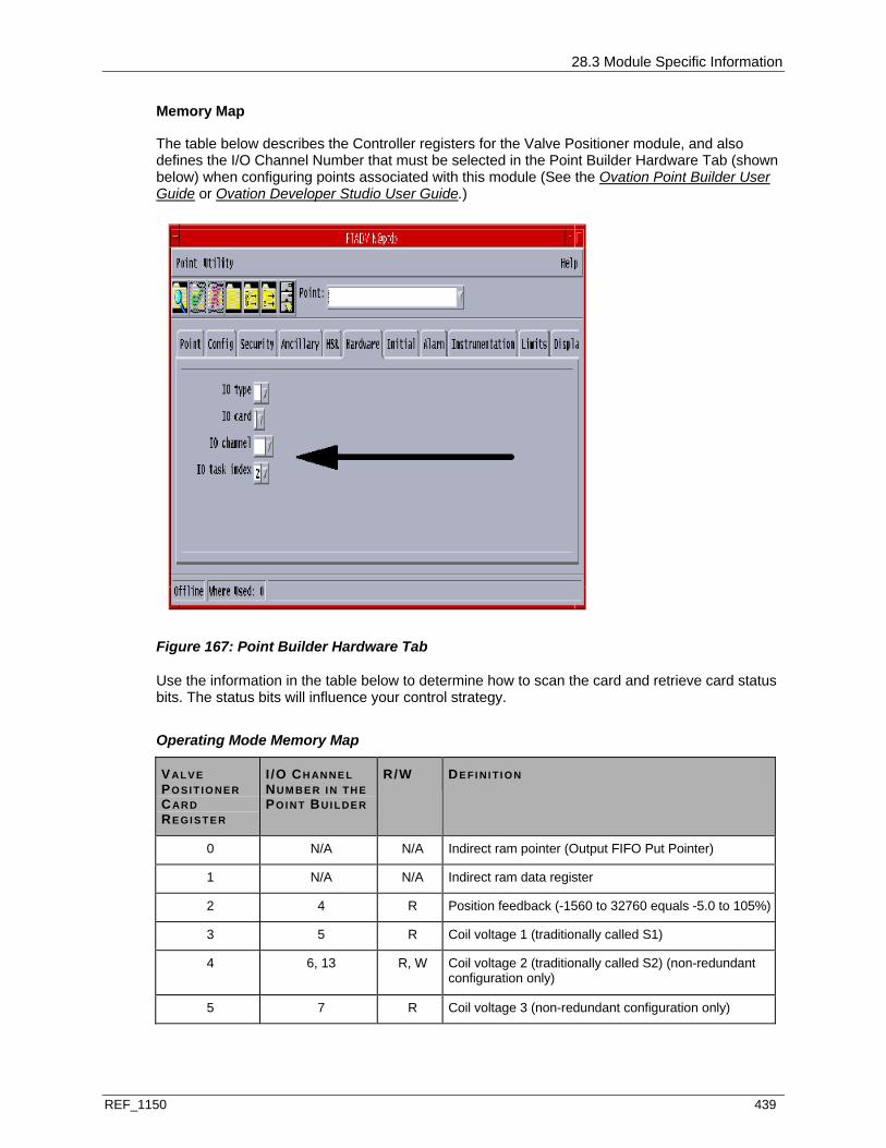
28.3 Module Specific Information
REF_1150 439
Memory Map
The table below describes the Controller registers for the Valve Positioner module, and also defines the I/O Channel Number that must be selected in the Point Builder Hardware Tab (shown below) when configuring points associated with this module (See the Ovation Point Builder User Guide or Ovation Developer Studio User Guide.)
Figure 167: Point Builder Hardware Tab
Use the information in the table below to determine how to scan the card and retrieve card status bits. The status bits will influence your control strategy.
Operating Mode Memory Map
VALV E PO SI T I O NE R CARD RE GI S T E R
I /O CH AN N E L NUM BE R I N TH E POI NT BUI L DE R
R/W DE FI NI T I O N
0 N/A N/A Indirect ram pointer (Output FIFO Put Pointer)
1 N/A N/A Indirect ram data register
2 4 R Position feedback (-1560 to 32760 equals -5.0 to 105%)
3 5 R Coil voltage 1 (traditionally called S1)
4 6, 13 R, W Coil voltage 2 (traditionally called S2) (non-redundant configuration only)
5 7 R Coil voltage 3 (non-redundant configuration only)
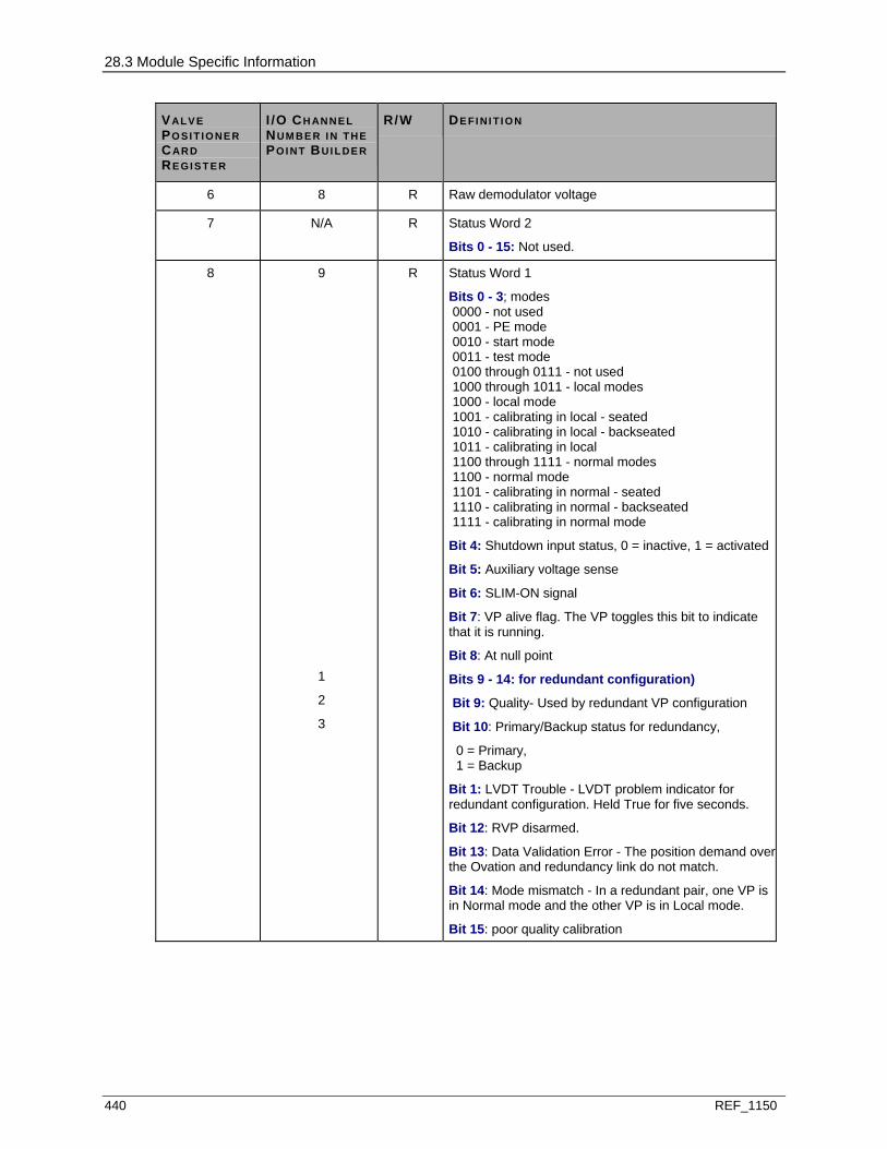
28.3 Module Specific Information
440 REF_1150
VALV E PO SI T I O NE R CARD RE GI S T E R
I /O CH AN N E L NUM BE R I N TH E POI NT BUI L DE R
R/W DE FI NI T I O N
6 8 R Raw demodulator voltage
7 N/A R Status Word 2
Bits 0 - 15: Not used.
8 9
1
2
3
R Status Word 1
Bits 0 - 3; modes 0000 - not used 0001 - PE mode 0010 - start mode 0011 - test mode 0100 through 0111 - not used 1000 through 1011 - local modes 1000 - local mode 1001 - calibrating in local - seated 1010 - calibrating in local - backseated 1011 - calibrating in local 1100 through 1111 - normal modes 1100 - normal mode 1101 - calibrating in normal - seated 1110 - calibrating in normal - backseated 1111 - calibrating in normal mode
Bit 4: Shutdown input status, 0 = inactive, 1 = activated
Bit 5: Auxiliary voltage sense
Bit 6: SLIM-ON signal
Bit 7: VP alive flag. The VP toggles this bit to indicate that it is running.
Bit 8: At null point
Bits 9 - 14: for redundant configuration)
Bit 9: Quality- Used by redundant VP configuration
Bit 10: Primary/Backup status for redundancy,
0 = Primary, 1 = Backup
Bit 1: LVDT Trouble - LVDT problem indicator for redundant configuration. Held True for five seconds.
Bit 12: RVP disarmed.
Bit 13: Data Validation Error - The position demand over the Ovation and redundancy link do not match.
Bit 14: Mode mismatch - In a redundant pair, one VP is in Normal mode and the other VP is in Local mode.
Bit 15: poor quality calibration
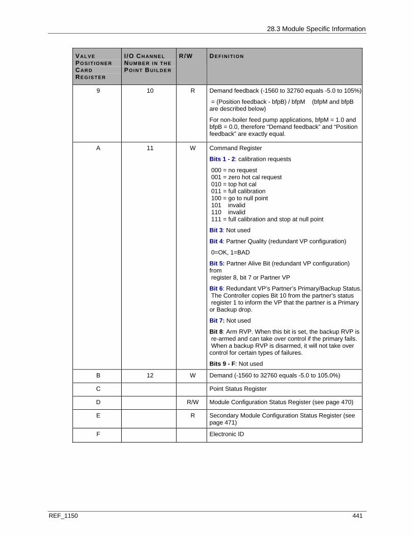
28.3 Module Specific Information
REF_1150 441
VALV E PO SI T I O NE R CARD RE GI S T E R
I /O CH AN N E L NUM BE R I N TH E POI NT BUI L DE R
R/W DE FI NI T I O N
9 10 R Demand feedback (-1560 to 32760 equals -5.0 to 105%)
= (Position feedback - bfpB) / bfpM (bfpM and bfpB are described below)
For non-boiler feed pump applications, bfpM = 1.0 and bfpB = 0.0, therefore “Demand feedback” and “Position feedback” are exactly equal.
A 11 W Command Register
Bits 1 - 2: calibration requests
000 = no request 001 = zero hot cal request 010 = top hot cal 011 = full calibration 100 = go to null point 101 invalid 110 invalid 111 = full calibration and stop at null point
Bit 3: Not used
Bit 4: Partner Quality (redundant VP configuration)
0=OK, 1=BAD
Bit 5: Partner Alive Bit (redundant VP configuration) from register 8, bit 7 or Partner VP
Bit 6: Redundant VP’s Partner’s Primary/Backup Status. The Controller copies Bit 10 from the partner’s status register 1 to inform the VP that the partner is a Primary or Backup drop.
Bit 7: Not used
Bit 8: Arm RVP. When this bit is set, the backup RVP is re-armed and can take over control if the primary fails. When a backup RVP is disarmed, it will not take over control for certain types of failures.
Bits 9 - F: Not used
B 12 W Demand (-1560 to 32760 equals -5.0 to 105.0%)
C Point Status Register
D R/W Module Configuration Status Register (see page 470)
E R Secondary Module Configuration Status Register (see page 471)
F Electronic ID
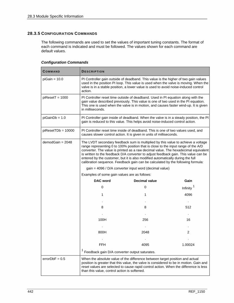
28.3 Module Specific Information
442 REF_1150
28.3.5 CONFIGURATION COMMANDS
The following commands are used to set the values of important tuning constants. The format of each command is indicated and must be followed. The values shown for each command are default values.
Configuration Commands
COMM AND DE S C RI P TI O N
piGain = 10.0 PI Controller gain outside of deadband. This value is the higher of two gain values used in the position PI loop. This value is used when the valve is moving. When the valve is in a stable position, a lower value is used to avoid noise-induced control action.
piResetT = 1000
PI Controller reset time outside of deadband. Used in PI equation along with the gain value described previously. This value is one of two used in the PI equation. This one is used when the valve is in motion, and causes faster wind-up. It is given in milliseconds.
piGainDb = 1.0
PI Controller gain inside of deadband. When the valve is in a steady position, the PI gain is reduced to this value. This helps avoid noise-induced control action.
piResetTDb = 10000 PI Controller reset time inside of deadband. This is one of two values used, and causes slower control action. It is given in units of milliseconds.
demodGain = 2048
The LVDT secondary feedback sum is multiplied by this value to achieve a voltage range representing 0 to 100% position that is close to the input range of the A/D converter. The value is printed as a raw decimal value. The hexadecimal equivalent is written to the feedback D/A converter to adjust feedback gain. This value can be entered by the customer, but it is also modified automatically during the full calibration sequence. Feedback gain can be calculated by the following formula:
gain = 4096 / D/A converter input word (decimal value)
Examples of some gain values are as follows:
DAC word Decimal value Gain
0 0 Infinity 1
1 1 4096
. . .
8 8 512
. . .
100H 256 16
. . .
800H 2048 2
. . .
FFH 4095 1.00024 1 Feedback gain D/A converter output saturates.
errorDbF = 0.5
When the absolute value of the difference between target position and actual position is greater that this value, the valve is considered to be in motion. Gain and reset values are selected to cause rapid control action. When the difference is less than this value, control action is softened.
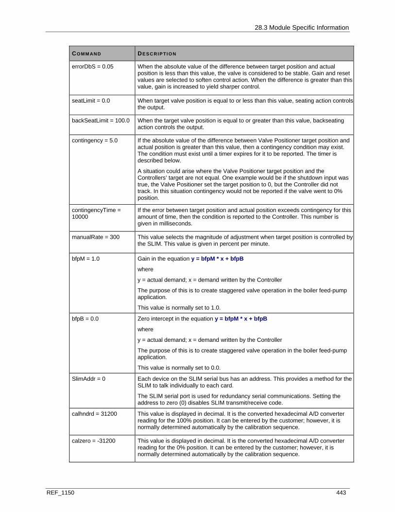
28.3 Module Specific Information
REF_1150 443
COMM AND DE S C RI P TI O N
errorDbS = 0.05
When the absolute value of the difference between target position and actual position is less than this value, the valve is considered to be stable. Gain and reset values are selected to soften control action. When the difference is greater than this value, gain is increased to yield sharper control.
seatLimit = 0.0 When target valve position is equal to or less than this value, seating action controls the output.
backSeatLimit = 100.0 When the target valve position is equal to or greater than this value, backseating action controls the output.
contingency = 5.0
If the absolute value of the difference between Valve Positioner target position and actual position is greater than this value, then a contingency condition may exist. The condition must exist until a timer expires for it to be reported. The timer is described below.
A situation could arise where the Valve Positioner target position and the Controllers’ target are not equal. One example would be if the shutdown input was true, the Valve Positioner set the target position to 0, but the Controller did not track. In this situation contingency would not be reported if the valve went to 0% position.
contingencyTime = 10000
If the error between target position and actual position exceeds contingency for this amount of time, then the condition is reported to the Controller. This number is given in milliseconds.
manualRate = 300
This value selects the magnitude of adjustment when target position is controlled by the SLIM. This value is given in percent per minute.
bfpM = 1.0 Gain in the equation y = bfpM * x + bfpB
where
y = actual demand; x = demand written by the Controller
The purpose of this is to create staggered valve operation in the boiler feed-pump application.
This value is normally set to 1.0.
bfpB = 0.0 Zero intercept in the equation y = bfpM * x + bfpB
where
y = actual demand; x = demand written by the Controller
The purpose of this is to create staggered valve operation in the boiler feed-pump application.
This value is normally set to 0.0.
SlimAddr = 0
Each device on the SLIM serial bus has an address. This provides a method for the SLIM to talk individually to each card.
The SLIM serial port is used for redundancy serial communications. Setting the address to zero (0) disables SLIM transmit/receive code.
calhndrd = 31200
This value is displayed in decimal. It is the converted hexadecimal A/D converter reading for the 100% position. It can be entered by the customer; however, it is normally determined automatically by the calibration sequence.
calzero = -31200
This value is displayed in decimal. It is the converted hexadecimal A/D converter reading for the 0% position. It can be entered by the customer; however, it is normally determined automatically by the calibration sequence.

28.3 Module Specific Information
444 REF_1150
COMM AND DE S C RI P TI O N
calrateF = 1664
This value is given in percent per minute and is the movement rate used when calibrating from the Laptop computer via the serial port. It is typically the Faster rate.
calrateS = 1664
This value is given in percent per minute and is the movement rate used when calibrating via a command from the Ovation I/O interface. It is typically the Slower rate.
Note
When the raise/lower button is pressed, the Valve Positioner will respond to the keystroke if the address is 1 through 8 inclusive. This means that all valves will move together.
posErrDelta = 5.0 A tunable parameter which sets a limit for the difference between target and actual position. When the difference is greater than this limit, POSITION ERROR FLAG is set TRUE, otherwise it is FALSE. This variable is similar to contingency except that it is devoted to the redundant calculations.
maxdelta = 5.0 A tunable parameter which sets a limit for the difference between position feedback and previous position feedback. The default value is 5%. Expressing the value as a derivative would yield 5% per 10 msec (= looptime) or 500% per second. This value is intended to represent the maximum rate of movement of the valve. This value has a function similar to MIN2NDRY. It is assumed that MAXDELTA will always be the smaller of the two.
min2ndry = 5.0 The minimum secondary value is similar to MAXDELTA because it represents a position feedback derivative. However, MIN2NDRY describes the minimum value in percent of a contribution of either secondary signal. If the secondary wire were to break, position feedback would suddenly change by at lease this amount. The default value is 10%. If the difference between position feedback and previous position feedback were to change by this value, or greater, it suggests a broken secondary wire. It is assumed that MIN2NDRY is larger than MAXDELTA.
lvdtTrack = 1.5 The maximum difference between LVDT readings in a redundant configuration.
RDNDNT If RDNDNT = 0, the VP is a standalone module
If RDNDNT = 1, the VP is a redundant module
This is the MOST important constant and MUST be set prior to inserting the VP into its mounting slot. If the VP is installed without this constant being set, and the unit is on line, the results are unpredictable.
In some cases, such as when a VP module is being replaced by another VP from stock, the VP should be placed into an unused slot to power it up and modify the constant. Remember to type SC to save the constants to EEPROM memory. Setting this constant changes the Baud Rate for COM Port 2 (SLIM port) to 25 k baud.
demand = 10.0 This command sets target value position to 10%, sets the VP made to local, and sets a restriction bit to prevent the VP from entering Normal mode. Type “EXIT” to clear the restriction bit.
CoilCount = 2 If CoilCount = 1, the VP is a redundant module and only coil 1 from the VP is used. Failure to set this constant will typically result in servo coil diagnostic failures, which cause the VP to fail to its Backup.
If CoilCount = 2, coils 1 and 2 are used, and coil 3 (diagnostic) is disabled.
diagtime = 20 Timer value in millisecond increments for the coil short/open timer. The conditions must exist for this amount of time before it is reported to the Controller.

28.3 Module Specific Information
REF_1150 445
COMM AND DE S C RI P TI O N
diags Displays status information in hexadecimal format. Included is the operating mode, restrictions, signals, and Severe Fatal Errors (SFE) bits. The following message is displayed:
mode=0xmmmm restrictions=0xrrrrrrr signals=0xssss sfe’s=0xeeee
where mmmm = Hex value of operating mode:
0 through 0x05 are start modes 0x14 through 0x19 are local modes 0x28 through 0x2B are normal modes 0x3C through 0x3F are test modes
rrrrrrr = Restriction bit array:
Bit 0 - PROM checksum error Bit 1 - Memory diagnostic error Bit 2 - A/D, D/A subsystem error Bit 3 - Contingency restriction Bit 4 - Ovation I/O not configured Bit 5 - Constants are mismatched Bit 6 - Controller is not updating Bit 7 - Controller is not tracking Bit 8 - EEPROM checksum error Bit 9 - Hold until oscillator is stable Bit 10 - Serial port control (local mode) restriction
ssss = Signal flags:
Bit 0 - Coil 1 diagnostic
Bit 1 - Coil 2 diagnostic Bit 2 - Coil 3 diagnostic Bit 3 - DAC diagnostic Bit 4 - Coil 1 open Bit 5 - Coil 1 short Bit 6 - Coil 2 open Bit 7 - Coil 2 short Bit 8 - Coil 3 open Bit 9 - Coil 3 short Bit A - AD/DA error Bit B - Contingency Bit C - Repetitive display Bit D - Raise pushbutton on SLIM Bit E - Lower pushbutton on SLIM
eeee = Severe fatal error bits:
Bit 0 - EEPROM checksum Bit 1 - PROM checksum Bit 2 - Shared memory error Bit 3 - Processor memory error Bit 4 - FPGA won’t program Bit 5 - UART readback error Bit 6 - Processor error Bit 7 - AD/DA error Bit 8 - PSD memory error Bit 9 - EE write sequence error

28.3 Module Specific Information
446 REF_1150
COMM AND DE S C RI P TI O N
kServo = 20.0 kServo is a parameter, given in percentage, that models the impedance relationship of the Personality module (PMOD) and the servo coil. For example, if the user has a PMOD with an impedance of 300 ohms, and the coil impedance is 82 ohms, then kServo should be set to 21.0 or 82 / (300 + 82). VP diagnostic firmware uses this parameter to predict coil voltage based on amplifier output voltage.
Wire impedance is included in coil impedance. The user can take a direct measurement with a standard voltmeter by removing the VP from the base unit. The user can also measure the ratio directly. One method is to measure amplifier output voltage at B13, a coil output that is normally unconnected, then measure coil voltage at B14 or B15. With the unit off line, amplifier voltage at B13 would be saturated to 10 volts or 5 volts depending on the state of the current reduction algorithm.
This parameter can be used when servo coils are wired in parallel. For this example, kServo would be set to 11.7 or 40 / (300 + 40). If one of the coils burned out, the relationship would change to 21.0. By setting kServoDb to 5.0, an alarm would be generated when the servo coil went open circuit.
kServoDb = 5.0
Deadband value used to calculate the allowable coil voltage range when comparing predicted voltage to actual voltage.
priorityDemand = -5.0 For firmware revisions 0H and later, “priorityDemand” is the target position used when the shutdown input is activated. The default value is selected so that upgraded modules are backward compatible. The user can set this value to an intermediate value in order to create his own scheme for handling of plant upsets.
28.3 Module Specific Information
REF_1150 447
28.3.6 SLIM (SMALL LOOP INTERFACE MODULE) INTERFACE
A standard SLIM (see page 407) is used to control a group of valves on a common serial bus).
Modes
The SLIM has four modes:
Local Auto Cascade Manual
Only two of the four (local and auto) correspond to Valve Positioner modes. Local mode corresponds to Valve Positioner local-manual mode. However, the operator does not request “local’ mode.” It is only entered when the Controller stops or fails to update the Valve Positioner card.
SLIM auto mode corresponds to Valve Positioner normal mode. In this mode, the Controller is writing its desired position to the Valve Positioner. In normal mode, the valves’ position and set point can be viewed on the SLIM, but the SLIM has no control over the Valve Positioner.
These modes should not be confused with auto and manual modes of software loops within the Controller. The important thing to remember is that the Valve Positioner is always in normal mode, receiving its position from the Controller, unless the Controller fails, in which case the Valve Positioner switches to local mode.
When raise and lower on the SLIM are pressed, all Valve Positioners respond to the key action. This means that all valves will move together as a group. It also suggests that no other devices (Loop Interfaces) should be connected on the serial bus with a group of Valve Positioners.
In abnormal situations, such as during maintenance, some valves may be in normal mode, and some may be in local mode. In this situation the valve in local mode will respond to raise/lower action, but the valves in normal mode will not. The Controller application will warn or notify the operator of the mode of each valve.
Since the SLIM will be connected to a group of Valve Positioners, each Valve Positioner must control its own transmit enable. Each SLIM enables its transmitter when placing a response into the transmit buffer. It also starts a 25 mSec timer, which, when expired, disables the transmitter.
SLIM PUSHBUTTONS
The purpose of this section is to highlight and clarify SLIM operation as it differs from normal operation when connected to the Ovation Loop Interface.
The actions that occur when a SLIM pushbutton is used are described in the table below.
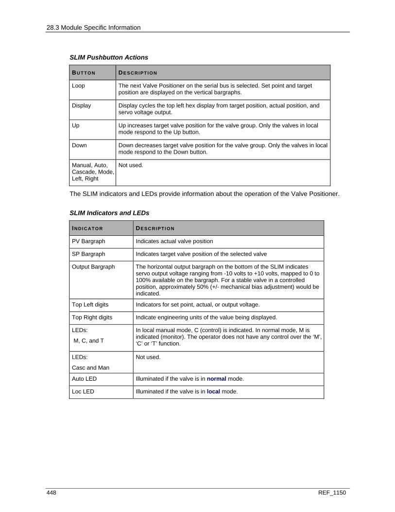
28.3 Module Specific Information
448 REF_1150
SLIM Pushbutton Actions
BU T T O N DE S C RI P TI O N
Loop The next Valve Positioner on the serial bus is selected. Set point and target position are displayed on the vertical bargraphs.
Display Display cycles the top left hex display from target position, actual position, and servo voltage output.
Up Up increases target valve position for the valve group. Only the valves in local mode respond to the Up button.
Down Down decreases target valve position for the valve group. Only the valves in local mode respond to the Down button.
Manual, Auto, Cascade, Mode, Left, Right
Not used.
The SLIM indicators and LEDs provide information about the operation of the Valve Positioner.
SLIM Indicators and LEDs
IN DI C ATO R DE S C RI P TI O N
PV Bargraph Indicates actual valve position
SP Bargraph Indicates target valve position of the selected valve
Output Bargraph The horizontal output bargraph on the bottom of the SLIM indicates servo output voltage ranging from -10 volts to +10 volts, mapped to 0 to 100% available on the bargraph. For a stable valve in a controlled position, approximately 50% (+/- mechanical bias adjustment) would be indicated.
Top Left digits Indicators for set point, actual, or output voltage.
Top Right digits Indicate engineering units of the value being displayed.
LEDs:
M, C, and T
In local manual mode, C (control) is indicated. In normal mode, M is indicated (monitor). The operator does not have any control over the ‘M’, ‘C’ or ‘T’ function.
LEDs:
Casc and Man
Not used.
Auto LED Illuminated if the valve is in normal mode.
Loc LED Illuminated if the valve is in local mode.

28.3 Module Specific Information
REF_1150 449
28.3.7 VALVE POSITIONER CONTROL
In normal, local, and calibrate modes the Valve Positioner is always controlling valve position. The PI routine runs unconditionally every 10 msec. Typically, it will execute the PI equation as described below. The PI routine has some conditionally executed parts to handle seating and backseating.
Seating and Backseating
Seating and backseating are important features of valve position control. The purpose of seating is to ensure that the hydraulic system is forcing the valve closed and admitting no steam into the turbine. Backseating is desirable because it can affect efficiency, and because, for certain valve assemblies, a leakoff into other steam systems are designed, assuming the valve is fully backseated.
The demand position from the Controller to the Valve Positioner is designed for a range of -5% to 105% and resolution exceeding 13 bits. Seating is in effect when the position demand is equal to or less than a programmable value, typically 0%, and actual position feedback is less than 5%. When seating is in effect, the output is driven to the maximum possible value in the direction that closes the valve. A timer is started. After 10 seconds, the output is reduced to 50% of the maximum value in the direction that closes the valve. A similar limit and function is provided for backseating.
With revision J, the behavior of backseating has changed, and an anti-windup feature is implemented that affects both seating and backseating.
With revision J and beyond, when the VP is seating or backseating, the integral accumulation is set to 0. The result is that when the target position returns to the normal operating range (seatLimit < targetPosition < backSeatLimit), the output voltage is 0.0 (plus proportional adjustment). In other words, the output voltage will jump to 0.0 and not require integration to bring the output back to a controlling value.
In conjunction with the straight line adjustment (implemented using bfpM and bfpB) of target position, a soft landing is implemented for backseating. When the target position exceeds backSeatLimit, the physical target position is ramped to the physical 100% position. At this point, the output voltage goes to 50%. The 10 seconds timing function is not implemented.
PI POSITION CONTROL
The equation for PI position control is:
⎥⎦
⎤⎢⎣
⎡+ ∫ dtte
kte
ipK )(1)(
where:
Kp = Proportional gain
KI = Integral time
e(t) = Position error
If seating or backseating is in effect, normal PI Controller calculation is halted.

28.3 Module Specific Information
450 REF_1150
SHUTDOWN INPUT (PRIORITY DEMAND INPUT)
Position control is affected by a shutdown input, intended to be used in emergency or abnormal situations. It is a standard 24 volt digital input circuit.
Typically, the Valve Positioner will rapidly drive the valve to the 0% position when the shutdown input is energized. The Valve Positioner then transfers to local-manual mode for the purpose of requiring the Controller to track position feedback. Once the Controller tracks, the Valve Positioner will transfer back to normal mode.
The state of the shutdown input is available to the Controller via a Valve Positioner module Ovation register.
A control bit in the shared memory can cause the Valve Positioner to ignore the shutdown input while in normal mode. This is used when the customer prefers trip logic in the Controller, not on the card. However, in local-manual mode, the Valve Positioner will drive the valve shut when the shutdown input is energized, regardless of the state, or previous state, of the control bit.
For VP firmware revisions 0H and later, the shutdown input is redefined to “Priority Demand Input.” When the input is activated, the target position is set to a tunable constant. For compatibility with previous firmware revisions, the default value of priority Demand is -5%.
This allows the user to rapidly move the valve to some intermediate position during upset conditions. The user has the flexibility to create his own scheme to handle an upset.
While the “priority demand input”, or “Shutdown” input is active, the VP is in the local mode and the controller must unconditionally track demand feedback.

28.4 Calibration
REF_1150 451
28.4 CALIBRATION
28.4.1 PERFORMING CALIBRATION USING THE SERIAL PORT
Using the Serial Port for Calibration, Settings
The local serial port is used in the field to calibrate and diagnose Valve Positioner problems. It is used in the factory to cause the Valve Positioner to perform necessary testing prior to shipment. This interface is implemented using the external UART.
The settings of the local serial port are:
Baud rate = 19200 Bits = 8 bits Stop Bits = One stop bit Parity = No parity
Status messages are printed during calibration sequences, such as:
‘Calibrate - Go to 100%’
OR
‘Calibrate - Reduce feedback gain’
WARNING! The EE memory can be corrupted if constants are modified during the calibration sequence. This occurs because the checksum is recalibrated based only on new values for 0%, 100% and feedback gain, not on the entire EE memory image.
Using the Serial Port for Calibration, Connections
The Personality module RS-232 connector is used to connect the Valve Positioner module to the COM1 or COM2 serial port of a personal computer.
Use cable 5A26448 or make a cable using the information in the table below.
RS-232 Connector (J2) Pin Assignments
PI N NUM BE R SI G N AL NAM E (FUNCTI O N) S I G N AL DI RECT I O N
1 Not used Not used
2 Not used Not used
3 TXD2/ (Transmit Data) Output
4 Not used Not used
5 RXD2/ (Receive Data) Input
6 GND (Logic Common) 1 Not used
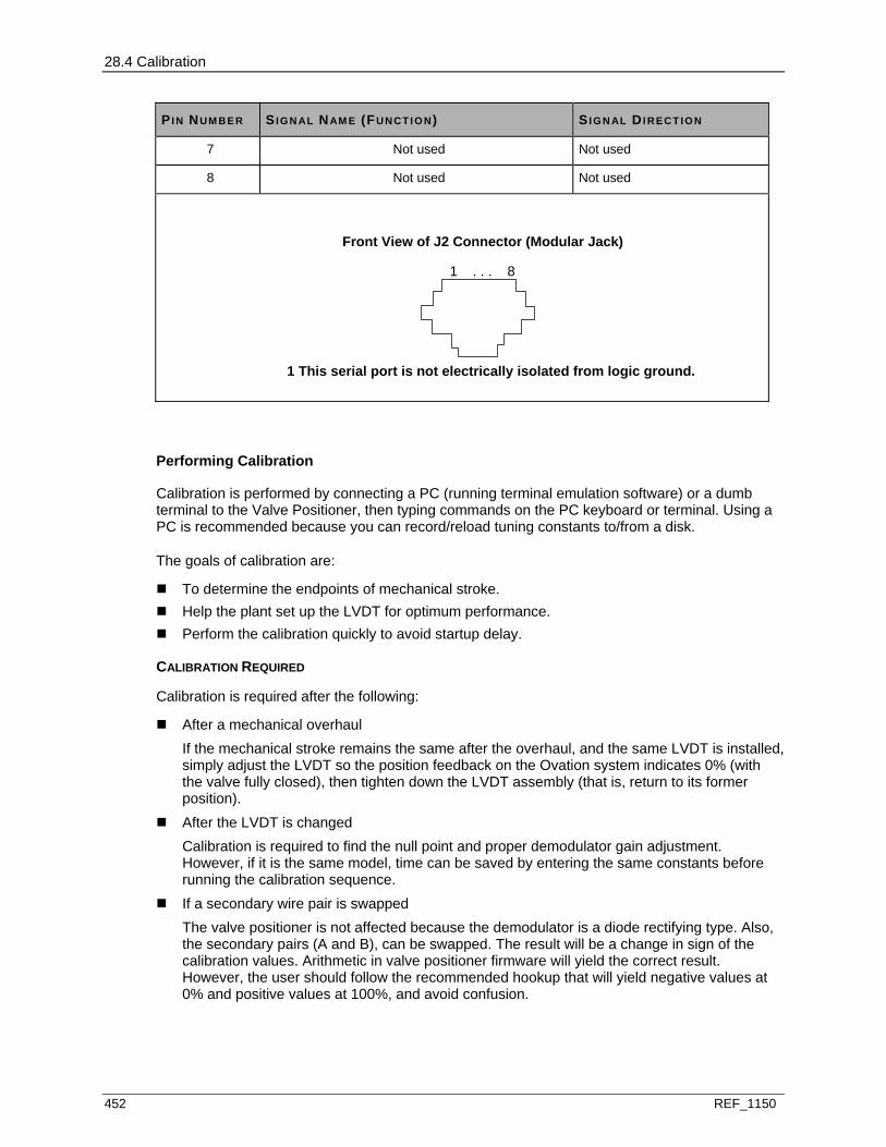
28.4 Calibration
452 REF_1150
PI N NUM BE R SI G N AL NAM E (FUNCTI O N) S I G N AL DI RECT I O N
7 Not used Not used
8 Not used Not used
Front View of J2 Connector (Modular Jack)
1 This serial port is not electrically isolated from logic ground.
1 . . . 8
Performing Calibration
Calibration is performed by connecting a PC (running terminal emulation software) or a dumb terminal to the Valve Positioner, then typing commands on the PC keyboard or terminal. Using a PC is recommended because you can record/reload tuning constants to/from a disk.
The goals of calibration are:
To determine the endpoints of mechanical stroke. Help the plant set up the LVDT for optimum performance. Perform the calibration quickly to avoid startup delay.
CALIBRATION REQUIRED
Calibration is required after the following:
After a mechanical overhaul If the mechanical stroke remains the same after the overhaul, and the same LVDT is installed, simply adjust the LVDT so the position feedback on the Ovation system indicates 0% (with the valve fully closed), then tighten down the LVDT assembly (that is, return to its former position).
After the LVDT is changed Calibration is required to find the null point and proper demodulator gain adjustment. However, if it is the same model, time can be saved by entering the same constants before running the calibration sequence.
If a secondary wire pair is swapped The valve positioner is not affected because the demodulator is a diode rectifying type. Also, the secondary pairs (A and B), can be swapped. The result will be a change in sign of the calibration values. Arithmetic in valve positioner firmware will yield the correct result. However, the user should follow the recommended hookup that will yield negative values at 0% and positive values at 100%, and avoid confusion.
28.4 Calibration
REF_1150 453
CALIBRATION IDEAL
During the calibration sequence, observe the valve to ensure it is moving, and that it is moving in the proper direction. Also, review the calibration constants and compare them with the ideal setup described below:
The range of calibration values corresponds to the hexadecimal range of the AD converter, and is presented to the user in decimal, ranging from -31768 to 31767.
When an LVDT is properly adjusted and calibrated, the calibration constants (0% and 100%) will be equal in amplitude and opposite in sign. The amplitudes for this ideal setup would be approximately 30,000. This result suggest the following:
The LVDT is adjusted so that its electrical null point (where secondary A amplitude = secondary B) matches the midpoint of the mechanical stroke.
The programmable gain amplifier on the demodulator is adjusted so that the electrical 'stroke' stays within the input range of the AD converter. Thus, the valve positioner can detect incremental movement for all valve positions.
If thermal expansion occurs, the valve positioner will continue to detect incremental movement, because the calibration is not to the extreme end of the AD converter range, and because the magnitude of thermal expansion is small.
TO SIMPLIFY DIAGNOSTICS
Rolled servo wires can cause the valve to move in the opposite direction. Be sure to observe and verify the correct movement of the valve. If only one pair is rolled, then the two pairs will be “fighting” each other. Use the following procedure to simplify diagnosis:
1. Disconnect one pair of wires.
2. Calibrate the valve, verifying the correct movement of the valve.
3. Reconnect the first pair of wires.
4. Disconnect the other pair of wires.
5. Calibrate the valve, verifying the correct movement of the valve.
6. Reconnect all the servo wires.
7. Calibrate the valve, verifying the correct movement of the valve.
ON-BOARD DIAGNOSTICS
The mechanical bias adjustment of the servo valve can affect the results of on-board diagnostics. A set-screw on the servo valve causes a deflection from center position of the servo valve spool. This allows hydraulic fluid to escape the actuator, and the valve to close at controlled rate, in the absence of an electrical signal.
For a typical hookup, a small negative voltage on the servo valve is required to center the spool, and hold the valve in a steady position. This voltage is typically from -100 to -300 mV. Servo valves are delivered from the factory with this adjustment. On board diagnostics assume that the servo valve is set up in this way. If another setup is used, program the Ovation Controller to ignore the results of diagnostic bits.
28.4 Calibration
454 REF_1150
WARNING - NOTES FOR GE 4-WIRE AND 5-WIRE SINGLE LVDT CONNECTIONS
The VP can detect position if only a single LVDT feedback signal is connected. The inputs of the unused LVDT input should be grounded to avoid picking up noise.
If LVDT A is connected, the 0% and 100% calibration constants will both be positive. If B is used, both constants will be negative.
GE style 4-wire and 5-wire LVDTs with 1 feedback can be connected so that 0% position is the high amplitude voltage (absolute value) and 100% is the low amplitude voltage. This is the desired connection since, in the event of a failure or broken wire, the VP will see a low voltage, assume the valve went open, and respond by closing the valve.
An alternate hookup can be implemented where 0% corresponds to the low amplitude voltage, and 100% corresponds to high amplitude. There are 2 problems with this setup.
1. Upon failure and loss of signal, the VP will attempt to open the valve to the target position because the valve appeared to close inappropriately.
2. During calibration the sequence starts at 0%, where the demodulator gain is raised until the feedback reaches the limit of the AD converter. The result will be a very high gain because the voltage at 0% is so low. Then, when the valve is moved to 100%, the voltage into the AD converter will be out of range, and the degree to which it is out of range is not detectable. The sequence will take a very long time to reduce the gain until the signal is usable, and the customer will be required to wait.
For a single LVDT hookup, the customer should complete the hookup, calibration, and then do the following test:
Set the valve position to an intermediate position, say 20%. Disconnect the oscillator wire. The valve should go closed.
TO PERFORM THE CALIBRATION PROCEDURE USING THE SERIAL PORT
1. Use a standard cable to make the connection (see page 451) between the PC (or dumb terminal) and the Valve Positioner.
2. Configure the serial port on the PC as described in “Settings (see page 451).”
3. To run a calibration sequence, perform the following:
a) A. Hook up the serial cable between the COM port and the user port on the Valve Positioner.
b) B. Start the terminal emulation software.
c) C. Ensure the settings are correct.
d) D. Type HELP<return> (See the table below).
Note the following:
Commands are case sensitive.
Syntax is strict.
There is no line buffering.
Backspace invalidates any typed command.
4. Type CALFULL<return> to run the full calibration sequence.
28.4 Calibration
REF_1150 455
5. If any constants are entered manually, type SC<return> to save the new constants to the EEPROM.
6. Use the command CALFULL after an overhaul, to fully calibrate the valve.
7. Use the command CALBOT just prior to startup, to reestablish the 0% calibration value if thermal expansion is detected.
Calibration Commands
COMM AND DE S C RI P TI O N
DC<return> Dump configuration constants from EEPROM.
SC<return> Save configuration constants to EEPROM.
DG<return> Display group 1 data - This function would repeatedly display important operating parameters such as demand, feedback, gain, and so forth.
HELP<return> Print command list.
EXIT<return> Exits test mode, raise/lower function, or calibration sequence. Causes a soft reset of the valve positioner.
28.4.2 PERFORMING CALIBRATION USING A GRAPHIC
Calibration can be performed by using the Valve Positioner Upload/Download/Calibrate graphic (diagram 8719) to view and modify the VP tuning constants. All the constants can be modified. The 0% and 100% calibration values, and demodulator gain, can be determined by the calibration sequence, and can be adjusted by the user with this graphic.
The graphic has upload/download buttons so that the two sets of numbers can be synchronized (made the same). This synchronization is initiated by the user and is the responsibility of the user. In addition to the constants, there are four fields that provide operator feedback.
The constants exist in two places:
EE memory on the Valve Positioner module. In the VPSTATUS algorithm record (typically, the constants contained in the algorithm record
are considered as the master set).
If a VP module fails and is replaced, the user simply downloads the constants to the new VP and it is ready to operate. The constants are not automatically copied to the algorithm record upon completion of a calibration sequence.
Note: Each constant shown on the graphic can also be entered through a serial port interface (see page 452).
Calibration Goals
The goals of calibration are:
To determine the endpoints of mechanical stroke.
Help the plant set up the LVDT for optimum performance.
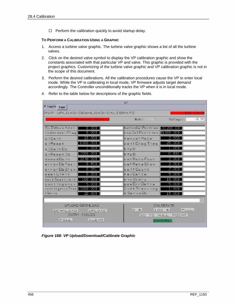
28.4 Calibration
456 REF_1150
Perform the calibration quickly to avoid startup delay.
TO PERFORM A CALIBRATION USING A GRAPHIC
1. Access a turbine valve graphic. The turbine valve graphic shows a list of all the turbine valves.
2. Click on the desired valve symbol to display the VP calibration graphic and show the constants associated with that particular VP and valve. This graphic is provided with the project graphics. Customizing of the turbine valve graphic and VP calibration graphic is not in the scope of this document.
3. Perform the desired calibrations. All the calibration procedures cause the VP to enter local mode. While the VP is calibrating in local mode, VP firmware adjusts target demand accordingly. The Controller unconditionally tracks the VP when it is in local mode.
4. Refer to the table below for descriptions of the graphic fields.
Figure 168: VP Upload/Download/Calibrate Graphic
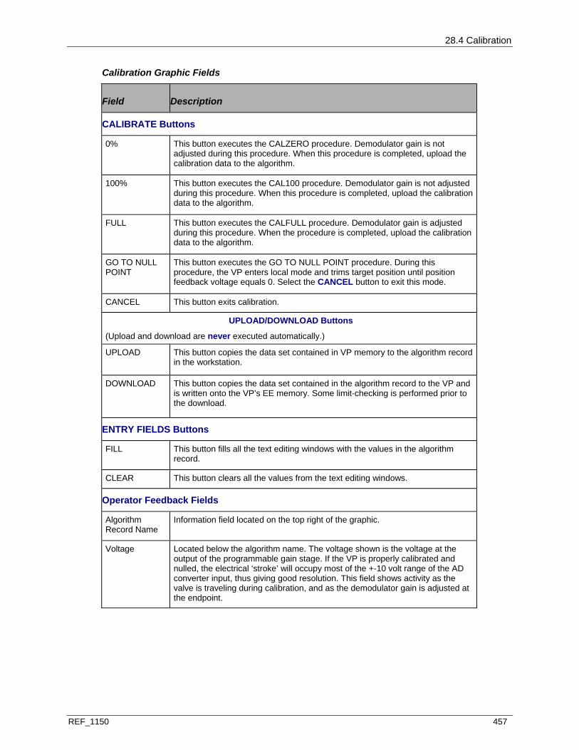
28.4 Calibration
REF_1150 457
Calibration Graphic Fields
Field Description
CALIBRATE Buttons
0% This button executes the CALZERO procedure. Demodulator gain is not adjusted during this procedure. When this procedure is completed, upload the calibration data to the algorithm.
100% This button executes the CAL100 procedure. Demodulator gain is not adjusted during this procedure. When this procedure is completed, upload the calibration data to the algorithm.
FULL This button executes the CALFULL procedure. Demodulator gain is adjusted during this procedure. When the procedure is completed, upload the calibration data to the algorithm.
GO TO NULL POINT
This button executes the GO TO NULL POINT procedure. During this procedure, the VP enters local mode and trims target position until position feedback voltage equals 0. Select the CANCEL button to exit this mode.
CANCEL This button exits calibration.
UPLOAD/DOWNLOAD Buttons
(Upload and download are never executed automatically.)
UPLOAD This button copies the data set contained in VP memory to the algorithm record in the workstation.
DOWNLOAD This button copies the data set contained in the algorithm record to the VP and is written onto the VP’s EE memory. Some limit-checking is performed prior to the download.
ENTRY FIELDS Buttons
FILL This button fills all the text editing windows with the values in the algorithm record.
CLEAR This button clears all the values from the text editing windows.
Operator Feedback Fields
Algorithm Record Name
Information field located on the top right of the graphic.
Voltage Located below the algorithm name. The voltage shown is the voltage at the output of the programmable gain stage. If the VP is properly calibrated and nulled, the electrical ‘stroke’ will occupy most of the +-10 volt range of the AD converter input, thus giving good resolution. This field shows activity as the valve is traveling during calibration, and as the demodulator gain is adjusted at the endpoint.

28.4 Calibration
458 REF_1150
Field Description
Mode (MA) Located to the left of the Voltage field. VP firmware is designed to stay in ‘normal’ mode, and if it is not in ‘normal’ mode, to establish communications with the Controller and then enter the ‘normal’ mode. In ‘normal’ mode, the VP receives its target position from the Controller.
The MA algorithm that drives the VP target position may be in AUTO, MANUAL, or LOCAL mode. When the VP is in ‘normal’ mode, it is not aware of the MA mode. It receives target position from the Controller in MA AUTO and MANUAL. The field will usually show AUTO unless there is an error condition or the VP enters local mode due to a calibration sequence.
During calibration, the VP enters local mode, which corresponds to MA local mode. The MA unconditionally tracks the VP until the calibration sequence completes.
When the operator selects a calibration sequence, the mode is shown as ‘local’. The voltage will change as the valve is moving. When the valve is at the endpoint and the demodulator gain is adjusting, the voltage will change as the gain is adjusted. A calibration complete message is displayed at the bottom field. In some cases in a full calibration, the results may yield poor values. A message will display telling the operator to repeat the calibration.
Valve Identification
Located to the left of the Mode field. Usually a text string that identifies the valve that is to be calibrated (name is provided by the turbine valve graphic).
Text Messages Located under the table of values. This field displays messages about the progress of the calibration. For example, “calibration in progress” or “calibration complete.”

28.4 Calibration
REF_1150 459
28.4.3 PERFORMING REDUNDANT VP CALIBRATION
VPs in a redundant subsystem can be calibrated as a pair or independently. The same commands are used to perform either calibration.
If you want to calibrate the VPs independently, the easiest method is to pull one of the VPs out of the mounting unit. In this case, calibration is the same as for a non-redundant VP. When a VP is calibrated and the Backup is not in service, and the RDNDNT flag is set, a warning message is printed to inform the operator that only one VP of the pair is being calibrated.
In any case, only the Primary VP or a pair can be calibrated. If you attempt to calibrate with the terminal connected to the Backup VP, the VP will print a message stating that the request is refused.
If you request a calibration of the Primary VP, and the Backup VP is also in service, the Backup is calibrated unconditionally. During calibration, the Primary disables the redundancy software state machine so failovers are eliminated.
The message packet exchange between the Primary and Backup VPs includes command/status bits related to calibration. The following table lists those commands and descriptions.
Redundant Calibration Commands
COMM AND DE S C RI P TI O N
RRVP_CAL_REC_TOP Primary VP is commanding the Backup VP to record the 100% endpoint value.
RRVP_CAL_REC_BOT Primary VP is commanding the Backup VP to record the 0% endpoint value.
RRVP_CAL_IN_ PROGRESS
Primary VP is informing the Backup VP that a calibration is in progress.
RRVP_CAL_BACKUP_ HOLD
Backup VP is performing a gain adjustment or is measuring the endpoint and is informing the Primary VP to wait for the process to be completed.
RRVP_CAL_WRITE_EE Primary VP is commanding the Backup VP to commit the new calibration data to EEPROM memory at the end of the calibration process.
RRVP_CAL_HOT Primary VP is informing the Backup VP that the calibration process is a “hot” calibration. A “hot” calibration is performed at only one end of the mechanical stroke. The important implication is that demodulator gain adjustment is not allowed during “hot” calibrations.
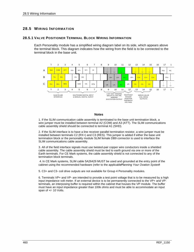
28.5 Wiring Information
460 REF_1150
28.5 WIRING INFORMATION
28.5.1 VALVE POSITIONER TERMINAL BLOCK WIRING INFORMATION
Each Personality module has a simplified wiring diagram label on its side, which appears above the terminal block. This diagram indicates how the wiring from the field is to be connected to the terminal block in the base unit.
Shd VS+COM ATT VF+ DI
LB+TX-
VF+
RX-
TX+ RX+ RES SHD
VS- DO
VS- RTN
LA+
LB- LA-
AC+
AC-
VP+
VP-
C1+
C1-
C2+
C2-
PS+ PS-
PS+
1 2 4 5
6 7 8 9 10 11 12 13 14 15 16 17 1
A
B
C
3 6 7 8 9 10 11 12 13 14 15 16 17 1
1 2 4 53
SLIM RS-485INTERFACE
SHUTDOWN DIGITAL INPUT& MANUAL DIGITAL OUPUT
LVDT SEC. WINDINGINPUTS & LVDT PRI.
WINDINGEXCITATION OUTPUT
TESTPOINTSCALED
POSITIONFEEDBACKVOLTAGE
SERVO-VALVECOIL DRIVEOUTPUTS
C3+
C3-
Notes1. If the SLIM communication cable assembly is terminated to the base unit termination block, awire jumper must be installed between terminal A2 (COM) and A3 (ATT). The SLIM communicationscable assembly shield should be connected to terminal A1 (SHD).
2. If the SLIM interface is to have a line receiver parallel termination resistor, a wire jumper must be installed between terminals C2 (RX+) and C3 (RES). This jumper is added if either the base unittermination block or the personality module SLIM female DB9 connector is used to interface theSLIM communications cable assembly.
3. All of the field interface signals must use twisted-pair copper wire conductors inside a shieldedcable assembly. The cable assembly shield must be tied to earth ground via one or more of the Earth terminals. For CE Mark systems, the cable assembly shield is not connected to any of thetermination block terminals.4. In CE Mark systems, SLIM cable 5A26429 MUST be used and grounded at the entry point of the
cabinet using the recommended hardware (refer to the applicable "Planning Your Ovation System."
5. C3+ and C3- coil drive outputs are not available for Group 4 Personality modules.
6. Terminals VP+ and VP- are intended to provide a test point voltage that is to be measured by a highinput impedance volt meter. If an external device is to be permanently connected to the VP+ and VP-terminals, an interposing buffer is required within the cabinet that houses the VP module. The buffermust have an input impedance greater than 100k ohms and must be able to accommodate an inputspan of +/- 10 Volts.
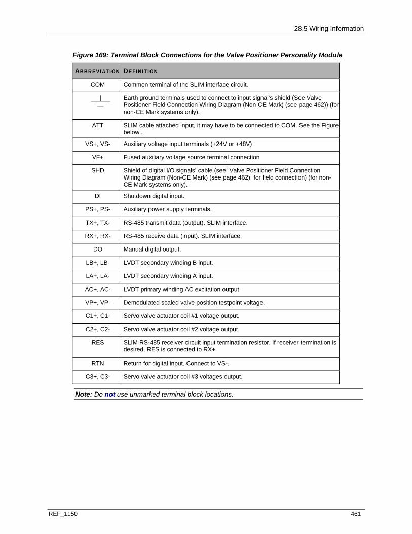
28.5 Wiring Information
REF_1150 461
Figure 169: Terminal Block Connections for the Valve Positioner Personality Module
AB B R E V I AT I ON DE FI NI T I O N
COM Common terminal of the SLIM interface circuit.
Earth ground terminals used to connect to input signal’s shield (See Valve Positioner Field Connection Wiring Diagram (Non-CE Mark) (see page 462)) (for non-CE Mark systems only).
ATT SLIM cable attached input, it may have to be connected to COM. See the Figure below .
VS+, VS- Auxiliary voltage input terminals (+24V or +48V)
VF+ Fused auxiliary voltage source terminal connection
SHD Shield of digital I/O signals’ cable (see Valve Positioner Field Connection Wiring Diagram (Non-CE Mark) (see page 462) for field connection) (for non-CE Mark systems only).
DI Shutdown digital input.
PS+, PS- Auxiliary power supply terminals.
TX+, TX- RS-485 transmit data (output). SLIM interface.
RX+, RX- RS-485 receive data (input). SLIM interface.
DO Manual digital output.
LB+, LB- LVDT secondary winding B input.
LA+, LA- LVDT secondary winding A input.
AC+, AC- LVDT primary winding AC excitation output.
VP+, VP- Demodulated scaled valve position testpoint voltage.
C1+, C1- Servo valve actuator coil #1 voltage output.
C2+, C2- Servo valve actuator coil #2 voltage output.
RES SLIM RS-485 receiver circuit input termination resistor. If receiver termination is desired, RES is connected to RX+.
RTN Return for digital input. Connect to VS-.
C3+, C3- Servo valve actuator coil #3 voltages output.
Note: Do not use unmarked terminal block locations.
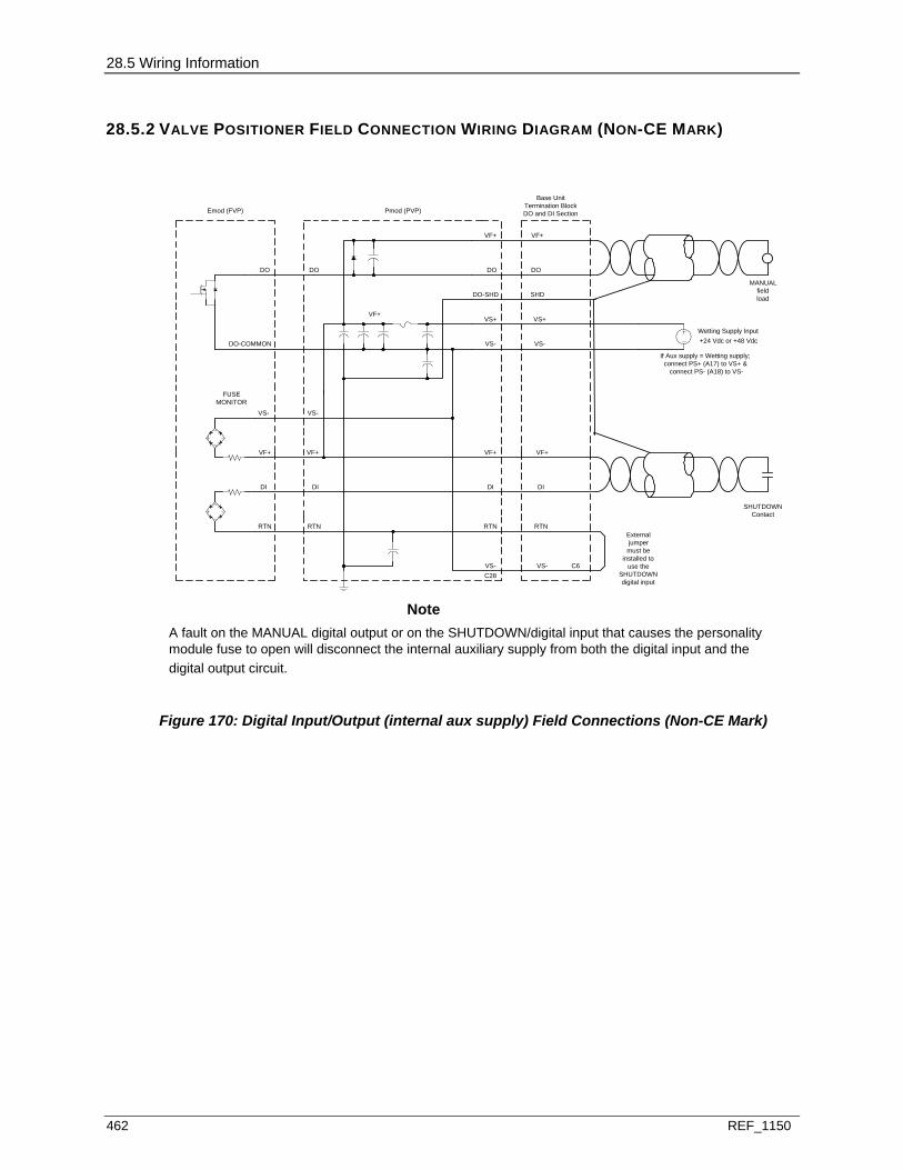
28.5 Wiring Information
462 REF_1150
28.5.2 VALVE POSITIONER FIELD CONNECTION WIRING DIAGRAM (NON-CE MARK)
NoteA fault on the MANUAL digital output or on the SHUTDOWN/digital input that causes the personalitymodule fuse to open will disconnect the internal auxiliary supply from both the digital input and the digital output circuit.
DO DO
DO-COMMON
VS+
VS-
DO
VF+
VF+
VF+
FUSEMONITOR
DO-SHD
MANUALfieldloadSHD
DO
VF+
VS+
VS-
Wetting Supply Input
If Aux supply = Wetting supply;connect PS+ (A17) to VS+ &
connect PS- (A18) to VS-
Base UnitTermination BlockDO and DI SectionPmod (PVP)Emod (FVP)
SHUTDOWNContact
VF+
DI
VF+
DI
C6
RTN
VS-C28
RTN
VS-
DI
RTNRTN
DI
Externaljumpermust be
installed touse the
SHUTDOWNdigital input
+24 Vdc or +48 Vdc
VS-
VF+
VS-
Figure 170: Digital Input/Output (internal aux supply) Field Connections (Non-CE Mark)
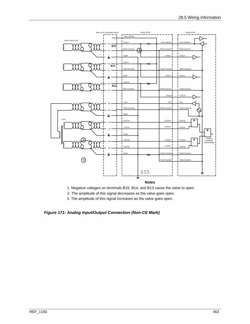
28.5 Wiring Information
REF_1150 463
COIL-DRIVE+COIL-DRIVE+
Field CommonField Common
COIL2+COIL2+
COIL1+COIL1+
COIL3+COIL3+
COIL-DRIVE+
COIL2+
Field Common
Field Common Field Common
Field Common Field Common
Earth
Earth
Earth
Field Common
Field Common
COIL1+
COIL3+
AC+AC+
Field Common Field Common
AC+
Field Common
0
0
0
0
0
0
0
0
LVDTA-
LVDTA+
Earth
LVDTA- LVDTA-
LVDTA+ LVDTA+
Earth
LVDTB-
LVDTB+ LVDTB+
LVDTB-LVDTB-
LVDTB+
Field Common
Field Common
Field Common
Field Common
Emod (FVP)Pmod (PVP)
C2+
C2-
C1+
C1-
C3+
C3-
Servo Valve Coils
Base Unit Termination Block
AC+
AC-
LA+
LA-
LB+
LB-
LVDT
0
0
0
0
PositionFeedback
Demodulator
A1, A2, B1,B2, C1, C2
1
2
3
Notes1. Negative voltages on terminals B15, B14, and B13 cause the valve to open.2. The amplitude of this signal decreases as the valve goes open.3. The amplitude of this signal increases as the valve goes open.
B14
B15
B13
Figure 171: Analog Input/Output Connection (Non-CE Mark)
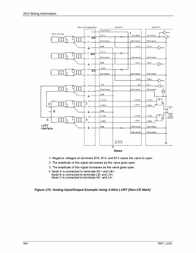
28.5 Wiring Information
464 REF_1150
Figure 172: Analog Input/Output Example Using 3-Wire LVRT (Non-CE Mark)
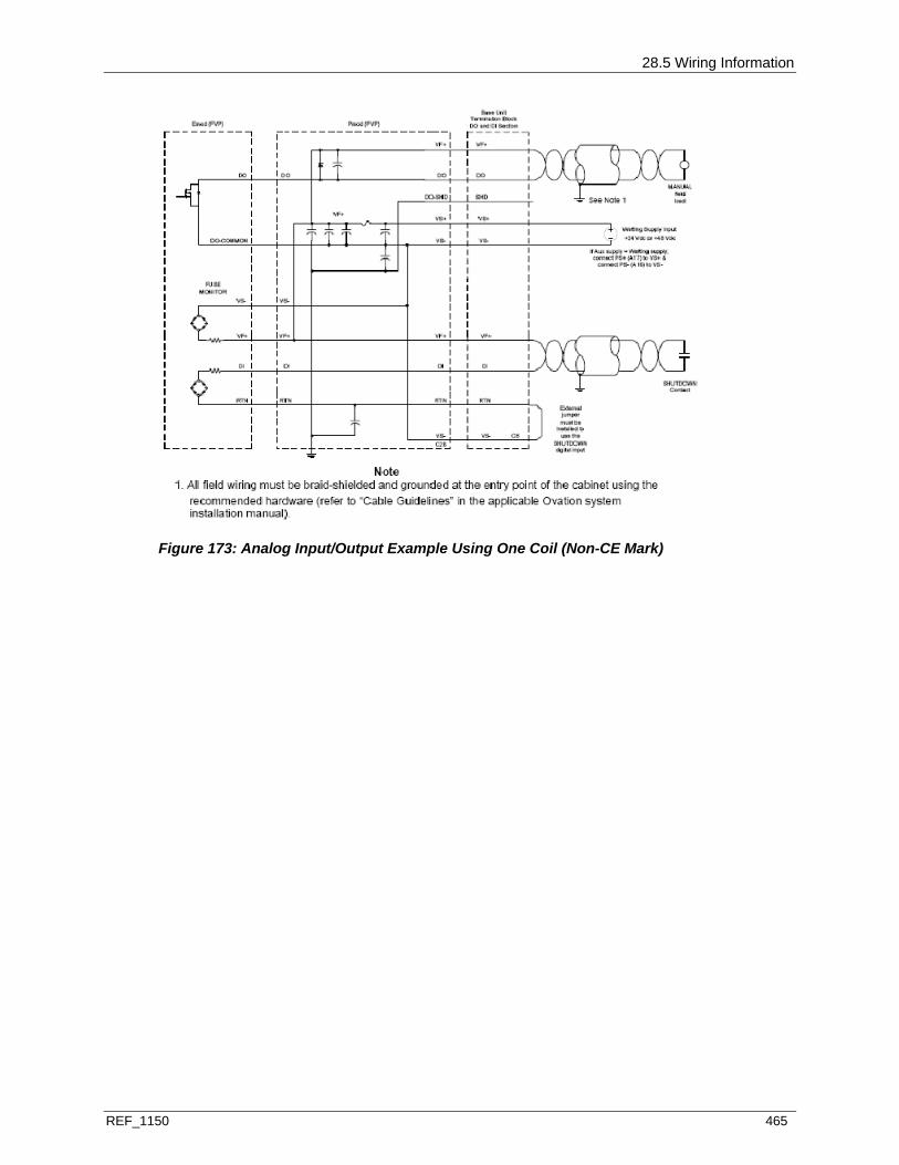
28.5 Wiring Information
REF_1150 465
Figure 173: Analog Input/Output Example Using One Coil (Non-CE Mark)
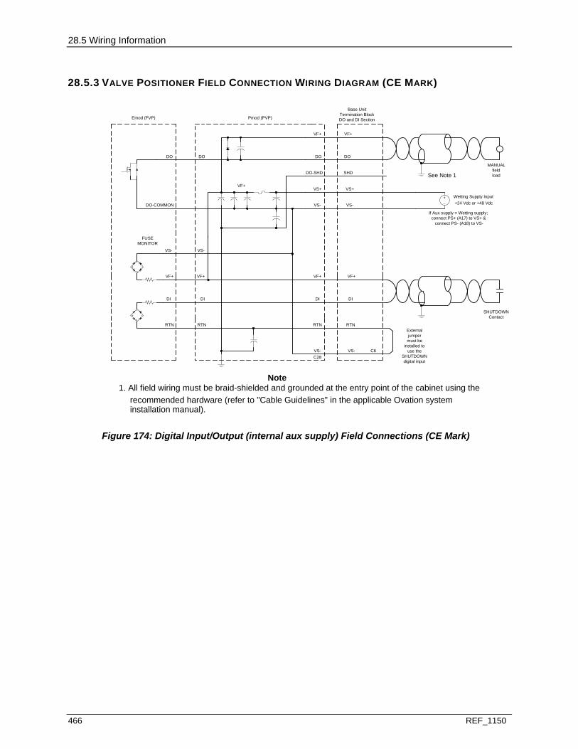
28.5 Wiring Information
466 REF_1150
28.5.3 VALVE POSITIONER FIELD CONNECTION WIRING DIAGRAM (CE MARK)
DO DO
DO-COMMON
VS+
VS-
DO
VF+
VF+
VF+
FUSEMONITOR
DO-SHD
MANUALfieldloadSHD
DO
VF+
VS+
VS-
Wetting Supply Input
If Aux supply = Wetting supply;connect PS+ (A17) to VS+ & connect PS- (A18) to VS-
Base UnitTermination BlockDO and DI SectionPmod (PVP)Emod (FVP)
SHUTDOWNContact
VF+
DI
VF+
DI
C6
RTN
VS-C28
RTN
VS-
DI
RTNRTN
DI
Externaljumpermust be
installed touse the
SHUTDOWNdigital input
+24 Vdc or +48 Vdc
VS-
VF+
VS-
See Note 1
1. All field wiring must be braid-shielded and grounded at the entry point of the cabinet using theNote
recommended hardware (refer to "Cable Guidelines" in the applicable Ovation systeminstallation manual).
Figure 174: Digital Input/Output (internal aux supply) Field Connections (CE Mark)

28.5 Wiring Information
REF_1150 467
COIL-DRIVE+COIL-DRIVE+
Field CommonField Common
COIL2+COIL2+
COIL1+COIL1+
COIL3+COIL3+
COIL-DRIVE+
COIL2+
Field Common
Field Common Field Common
Field Common Field Common
Earth
Earth
Earth
Field Common
Field Common
COIL1+
COIL3+
AC+AC+
Field Common Field Common
AC+
Field Common
0
0
0
0
0
0
0
0
LVDTA-
LVDTA+
Earth
LVDTA- LVDTA-
LVDTA+ LVDTA+
Earth
LVDTB-
LVDTB+ LVDTB+
LVDTB-LVDTB-
LVDTB+
Field Common
Field Common
Field Common
Field Common
Emod (FVP)Pmod (PVP)
C2+
C2-
C1+
C1-
C3+
C3-
Servo Valve Coils
Base Unit Termination Block
AC+
AC-
LA+
LA-
LB+
LB-
LVDT
0
0
0
0
PositionFeedback
Demodulator
A1, A2, B1,B2, C1, C2
2
3
4
Notes
B14
B15
B13
C
B
A
LVRTInterface
1. All field wiring must be braid-shielded and grounded at the entry point of the cabinet using the recommended hardware (see "Cable Guidelines" in applicable Ovation installation manual).2. Negative voltages on terminals B15, B14, and B13 cause the valve to open.3. The amplitude of this signal decreases as the valve goes open.4. The amplitude of this signal increases as the valve goes open.5. Node A is connected to terminals AC+ and LB+, Node B is connected to terminals LB- and LA+, Node C is connected to terminals AC- and LA-.
Figure 175: Analog Input and Analog Output Connection (CE Mark)
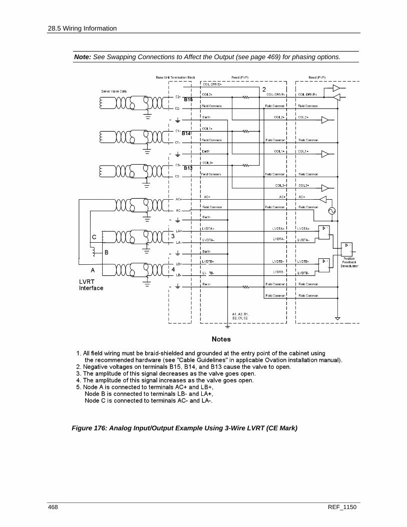
28.5 Wiring Information
468 REF_1150
Note: See Swapping Connections to Affect the Output (see page 469) for phasing options.
Figure 176: Analog Input/Output Example Using 3-Wire LVRT (CE Mark)
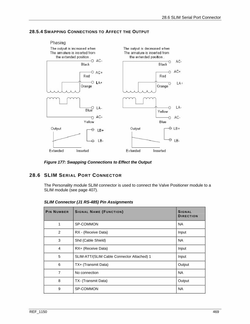
28.6 SLIM Serial Port Connector
REF_1150 469
28.5.4 SWAPPING CONNECTIONS TO AFFECT THE OUTPUT
Figure 177: Swapping Connections to Effect the Output
28.6 SLIM SERIAL PORT CONNECTOR
The Personality module SLIM connector is used to connect the Valve Positioner module to a SLIM module (see page 407).
SLIM Connector (J1 RS-485) Pin Assignments
PI N NUM BE R SI G N AL NAM E (FUNCTI O N) S I G N AL DI RE C TI O N
1 SP-COMMON NA
2 RX - (Receive Data) Input
3 Shd (Cable Shield) NA
4 RX+ (Receive Data) Input
5 SLIM-ATT/(SLIM Cable Connector Attached) 1 Input
6 TX+ (Transmit Data) Output
7 No connection NA
8 TX- (Transmit Data) Output
9 SP-COMMON NA
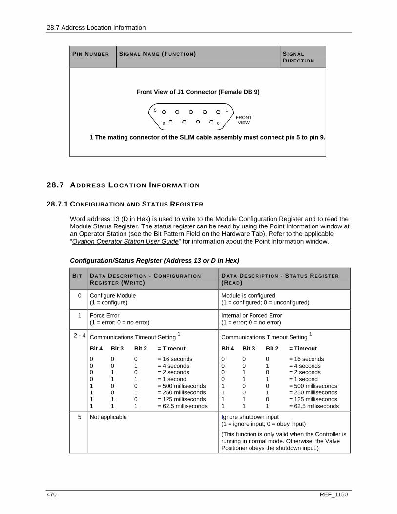
28.7 Address Location Information
470 REF_1150
PI N NUM BE R SI G N AL NAM E (FUNCTI O N) S I G N AL DI RE C TI O N
Front View of J1 Connector (Female DB 9)
1 The mating connector of the SLIM cable assembly must connect pin 5 to pin 9.
15
9 6FRONTVIEW
28.7 ADDRESS LOCATION INFORMATION
28.7.1 CONFIGURATION AND STATUS REGISTER
Word address 13 (D in Hex) is used to write to the Module Configuration Register and to read the Module Status Register. The status register can be read by using the Point Information window at an Operator Station (see the Bit Pattern Field on the Hardware Tab). Refer to the applicable “Ovation Operator Station User Guide” for information about the Point Information window.
Configuration/Status Register (Address 13 or D in Hex)
BI T DAT A DE S C R I P T I O N - CO NF I G U R AT I O N RE GI S T E R (WRI T E)
DAT A DE S C R I P T I O N - ST ATUS REGI S TER (RE AD)
0 Configure Module (1 = configure)
Module is configured (1 = configured; 0 = unconfigured)
1 Force Error (1 = error; 0 = no error)
Internal or Forced Error (1 = error; 0 = no error)
2 - 4 Communications Timeout Setting 1
Bit 4 Bit 3 Bit 2 = Timeout
0 0 0 = 16 seconds 0 0 1 = 4 seconds 0 1 0 = 2 seconds 0 1 1 = 1 second 1 0 0 = 500 milliseconds 1 0 1 = 250 milliseconds 1 1 0 = 125 milliseconds 1 1 1 = 62.5 milliseconds
Communications Timeout Setting 1
Bit 4 Bit 3 Bit 2 = Timeout
0 0 0 = 16 seconds 0 0 1 = 4 seconds 0 1 0 = 2 seconds 0 1 1 = 1 second 1 0 0 = 500 milliseconds 1 0 1 = 250 milliseconds 1 1 0 = 125 milliseconds 1 1 1 = 62.5 milliseconds
5 Not applicable Ignore shutdown input (1 = ignore input; 0 = obey input)
(This function is only valid when the Controller is running in normal mode. Otherwise, the Valve Positioner obeys the shutdown input.)
28.7 Address Location Information
REF_1150 471
6 Redundant RVP Link Status Bit (1=good; 0=bad)
Redundant RVP Link Status Bit (1=good; 0=bad)
7 Not applicable Severe Fatal Error - Check Register E
8 Not applicable Coil 1 may be shorted
9 Not applicable Coil 2 may be shorted
10 Not applicable Coil 3 may be shorted
11 Not applicable Coil 1 may be open
12 Not applicable Coil 2 may be open
13 Not applicable Coil 3 may be open
14 Not applicable Contingency (1 = contingency; 0 = no contingency)
15 Not applicable Handshake bit for download of calibration data
1 The tolerance on the timeout period is +/- 35%.
28.7.2 SECONDARY CONFIGURATION AND STATUS REGISTER
Word address 14 (E in Hex) provides for additional module configuration and module status. The bit definitions for this register are encoded as shown in Table.
Secondary Configuration/Status Register (Address 14 or E in Hex)
BI T DAT A DE S C R I P T I O N -
CO N FI G U R AT I O N REGI S TE R (WRI TE)
DAT A DE S C R I P T I O N -
ST AT US RE GI S T E R (RE AD)
0 Not applicable EEPROM checksum error
1 Not applicable PSD 302 EPROM checksum error
2 Not applicable Shared memory readback error
3 Not applicable Processor memory readback error
4 Not applicable FPGA error
5 Not applicable UART error
6 Not applicable Processor diagnostic error
7 Not applicable Coil drive D/A converter output readback error
8 Not applicable PSD 302 RAM error
9 Not applicable EEPROM write error
10 - 15 Not used Not used
28.8 Diagnostics
472 REF_1150
28.8 DIAGNOSTICS
One important feature of the servo valve is an adjustable mechanical bias mechanism. This mechanism creates a slight deflection in the valve spool so that a small amount of hydraulic fluid can escape the actuator and close the valve. Therefore, if there is no voltage applied to the servo valve, the actuator will slowly move toward the closed position. This deflection is typically overcome by -200 millivolts, so that when the valve is positioned and steady, this small voltage is seen on the servo valve.
The servo valve has two voltage coils, either of which can deflect the spool when excited. The combination of these features provides a redundancy feature that protects against broken wires or shorted coils, the ability to be diagnosed, and a predictable shutdown mechanism in the event the firmware diagnoses a catastrophic error and executes a shutdown, or an error mode occurs that allows a hardware watchdog timer to expire and de-power the Electronics module’s FVP field card.
The Valve Positioner continuously runs diagnostics to ensure that the circuit is operating properly. Certain conditions can cause the Valve Positioner to “dive,” essentially removing the output signal and allowing the valve to drift shut.
As a general rule, the card will view error conditions on start up as “no-go” or fatal errors. This means that the Valve Positioner will not generate an output to the valve. See the following error descriptions for specifics.
28.8.1 DA READBACK ERROR
The Valve Positioner has the ability to read and convert the coil drive D/A convertor output signal that drives the valve. If the value readback (converted by the A/D converter) and the value that was output do not match within a deadband, and for a pre-defined period of time, a severe fatal error is assumed. In this case, the Valve Positioner is “flying blind.” It cannot confidently determine valve position or control the output. The Valve Positioner will remove drive power (dive) from the entire Electronics module’s FVP field card and go through a reset sequence. The coil drive D/A convertor readback check is a diagnostic that runs continuously.
EPROM Checksum Error
The EPROM checksum check runs continuously as a low priority function. Failure of the checksum diagnostic is considered a severe fatal error.
Contingency Check Error
Contingency is defined as the difference between a target position and the actual position, when that difference is greater than a defined limit. In the Valve Positioner, the contingency bit is set if the difference exceeds a programmable limit (default value is 5%) for a programmable time period (default value is 10 seconds). Contingency is not a fatal condition.
Memory Read/Write Check Error
A failure of any memory to read back correctly is considered a severe fatal error.
28.8 Diagnostics
REF_1150 473
Open Coil Diagnostic Error
An open coil is detected by measuring voltage across the current limiting resistors on the servo output. When zero volts are detected, either the coil is open, the servo output is at zero, or the mechanical bias on the servo valve has been adjusted to yield that result. When an error condition is detected, an internal “open” bit is set.
For firmware revisions prior to 0F, the diagnostic works as described below. For later revisions, servo coil voltage is measured and compared to a model described by tuning constants “kServo” and “kServoDb.” If the voltage does not fit into the model, due to being too large, “open coil” is blamed and the internal diagnostic bit is set. Then the timing sequence described below is used to post the error bit to the controller.
Typically, the servo coil voltage is -200 mV when the valve is in a stable, controlled position and the servo valve mechanical bias is properly adjusted. If the servo output amplifier voltage amplitude falls below 100 mV, the internal bit is cleared, as though no error condition exists. If servo output voltage is greater than 100 mV, the difference between servo output voltage and coil voltage is compared to 50 mV, and if it is less, the ‘open’ bit is set.
If the open bit stays set for five seconds, the error condition is reported to the Controller in the module status register.
Shorted Coil Diagnostic
For each of the three coil outputs, an internal shorted bit is set if the converted value of terminal voltage is near 0 volts. Behavior of this diagnostic changes when servo output amplifier voltage is near zero.
For firmware revisions prior to 0F, the diagnostic works as described below. For later revisions servo coil voltage is measured and compared to a model described by tuning constants “kServo” and “kServoDb”. If the voltage does not fit into the model, due to being too large, “open coil” is blamed and the internal diagnostic bit is set. Then the timing sequence described below is used to post the error bit to the Controller.
Typically, the servo output coil is -200 mV when the valve is in a stable, controlled position and the servo valve mechanical bias is properly adjusted. If the servo output amplifier voltage falls below 50 mV, the internal bit is cleared, as though no error condition exists.
For servo output voltages greater in amplitude than 400 mV, the module status register voltage is compared to 50 mV, and a shorted bit is set if it is less. If the shorted coil bit remains active for five seconds, the condition is reported to the Controller in status word 1.
For servo amplifier voltage values between 50 and 400 mV, the comparison value is calculated as the servo amplifier voltage divided by eight. The timing described above is used. When the shorted bit becomes inactive, the corresponding bit in status word 1 is cleared immediately.

28.9 Troubleshooting
474 REF_1150
Diagnostics of LVDT Problems for Redundant VP
Diagnosing an LVDT failure is complex. Depending on the failure, the valve may go open, closed, or to a different intermediated position, which can be above or below the target position. If the valve is positioned at the LVDT null point, an oscillator failure would not be detected because the position feedback would continue to be equal to zero (0) volts.
If |(Position Feedback - Previous Position Feedback)| < MAXDELTA, and POSITIONERRORFLAG is not set, all conditions are considered normal, and the REDUNDANCY STATE is set to NORMAL. Previous Position Feedback is set equal to Position Feedback prior to exiting the PI routine.
If (Position Feedback - Previous Position Feedback) > MIN2NDRY and the backup is OK, the VP executes the failover.
If |(Position Feedback - Previous Position Feedback)| > MAXDELTA, a problem is suspected. VP firmware refuses to “believe” the new position feedback value, and does not update Previous Position Feedback or run the PI loop. If REDUNDANCY STATE is NORMAL, it is updated to POOR. If it is POOR, it is updated to BAD. If it is BAD, and the backup is OK, the VP executes the failover. This means that it can take 30 msec for the VP to determine that it should execute its failover.
If POSITION ERROR FLAG is set, and the partner’s reported position is within LVDTTRACKING of Position Feedback, the condition is not due to a failed LVDT, but for another reason. No action to fail over is taken.
If POSITION ERROR FLAG is set, and both Position Feedback voltage and Previous Position Feedback voltage are equal or close to zero volts, the problem is suspected to be a failed oscillator, or broken oscillator wire, and the failover is executed as long as the Backup is OK.
If POSITION ERROR FLAG is set, and Position Feedback differs from Partner’s Position Feedback by more than LVDTTRACKING, and the Backup is OK, an LVDT problem is suspected and the failover is executed.
28.9 TROUBLESHOOTING
28.9.1 ONLINE VP REPLACEMENT
A Valve Positioner module can be replaced online when the module fails.
Use the following procedure to remove an VP module and safely install a replacement module.
CAUTION! Observe all the precautions and then modify the procedure steps to suit your particular situation.
Precautions
If the valve is closed, isolate it hydraulically to prevent any bump when inserting the new VP.
Switch the MA driving the VP position to manual, and move the target position to zero. This is done to avoid jostling the valve when the new VP is inserted.
For large machines, switch the valves to ‘single’ or ‘full arc’ mode from ‘sequential’ or ‘partial arc’ mode.
Keep first stage, or impulse pressure, control loops in service to respond to any upset during the maintenance.
28.9 Troubleshooting
REF_1150 475
If the replacement is due to a suspected or intermittent problem, that can only be corrected by replacement, but the VP is operating, first close the valve by switching the MA to manual, driving the valve to 0%, and then isolate it hydraulically.
To Replace an Online VP
1. Once the valve is closed and in a safe condition, remove the bad VP.
2. Insert the replacement VP into the base unit.
3. Download constants using the Valve Positioner Upload/Download/Calibrate graphic.
4. View the reported feedback position. It should be close to 0%. If it is, the valve can be operated without calibration.
5. View the servo voltage at terminal screws 14B and C, and 13B and C. Note that if the servo voltage has integrated to a few volts negative, and hydraulic fluid is applied suddenly, the valve will ‘pop’, and the on-board PI will respond and bring the valve back to the target position of 0%. If the target position of 0% is less than ‘seatLimit’, servo voltage will be positive, thus driving the valve hard to the seat.
6. With the valve closed, you can execute the 0% calibration sequence to find the exact reading for the 0% position. If you believe the 100% calibration is close, the valve can then be operated without calibrating the 100% position, since there is little flow change when the valve is fully opened.
7. Verify that the VP is in the normal operating mode as indicated by the card edge LED.
8. When you determine that it is time to operate the valve, un-isolate the valve hydraulically, drive the target position of the MA to the desired position, and then switch the MA back to ‘auto.’
28.9.2 DEMODULATOR GAIN
Demodulator gain directly affects the calibration values at the endpoints. Reducing demodulator gain can be helpful in diagnosing VP problems. Note that the VP must be re-seated, or must be reset, in order to make any new demodulator gain setting effective.
A simple test can be performed to verify correct wiring and polarity.
1. Set 0 and 100% calibration values to –31000 and +31000.
2. Reduce demodulator gain to a low value (2000).
3. Reseat or reset the VP to cause the new demodulator gain to take effect.
4. Set target position to 0%, 100%, then 50% and observe valve movement at all settings.
28.9 Troubleshooting
476 REF_1150
In this test, you are informing the VP that the electrical valve ‘stroke’ is +/- 10 volts, but you have adjusted demodulator gain so that the actual electrical stroke is much smaller. (Perhaps +/- 1 volt, depending upon the LVDT.) The idea is to force the actual electrical ‘stroke’ to be fully contained within the range of the VP input system.
By setting the target position to 0% or 100%, you can verify correct wiring and polarity. If the valve goes to the correct endpoints, then you should set the target position to 50% as an additional test. The valve should go to the LVDT’s midpoint and hold there.
If the valve does not go to the correct endpoint, then there is a wiring error, and you should first remove one of the servo wire pairs, and repeat the test. The next step would be to swap the wires of the remaining servo wire pair, followed by swapping the wire pairs of LVDT input A with input B.
When the valve moves correctly, verify that the valve operates according to the recommended practice where negative voltage opens the valve, and positive voltage closes it.
During Automatic Calibration
Another problem with demodulator gain can occur during automatic calibration. When the value is backseated and demodulator gain is undergoing an adjustment, it is also predicting the new calibration value at the seated position. If the seated position goes out of range, then the value is cilpped and the user receives a message that a new calibration is necessary.
One of the underlying assumptions of the VP is that, in the worst case, the user positions the LVDT so that the 100% position is at the end of the linear range of the LVDT (possibly non-linear and accurate). Then during calibration, the firmware accepts a value of 100% that is higher in magnitude than the 0% calibration value. If the LVDT is not positioned this way, then you may receive a message that the calibration must be repeated.
If LVDT is not adjusted in this fashion, the user can enter his own demodulator gain, reseat the VP, then perform both the 0% and 100% endpoint calibration. If the results do not yield a calibration value approaching the endpoint, then demodulator gain can be increased, and the process repeated.
28.9.3 LVDT WIRING PROBLEMS (6-WIRE LVDT)
When an LVDT is wired incorrectly, it is typically a case where secondary pair A is swapped with secondary pair B.
The LVDT inputs on the VP are implemented with an amplifier stage that includes diode rectification. Therefore, the two individual wires of a secondary can be swapped and it makes no difference to the VP.
The wires of the excitation oscillator could also be swapped with no effect. The excitation coil and secondary coils are all isolated, so the VP can see only the AC component.
If the secondaries are wired correctly, and the LVDT is in approximately the correct position, feedback voltage shown on the VP calibration graphic is negative when the valve is closed, and positive when the valve is open.
The position feedback voltage is also available on terminals B12 and C12. This signal is used for factory testing and can be used for response testing in the field. It is inverted from the signal shown on the calibration graphic. (One way to avoid confusion is to connect voltmeter GND to B12, and voltmeter input to C12.)

28.10 Diagnostic LEDs
REF_1150 477
28.9.4 SERVO WIRING PROBLEMS
Valve Wired Backwards
If a servo valve is wired backwards (that is, the wire pair is rolled), the valve will move in the opposite direction. This is a positive feedback situation. The movement of the valve does not cure the position error, it increases it, thus causing the output voltage to move even faster, and drive the valve harder in the wrong direction.
One Pair of Servo Coil Wires, Wired Incorrectly
Another problem is with dual coil servo valves when one pair is wired correctly, and the other is rolled. Thus, the wire pairs are in opposition, and valve movement is indeterminate.
Use the following procedure to correct this problem:
1. Disconnect one of the pairs, since the valve will move with only one pair connected (typically, the first step when diagnosing wiring problems).
2. Calibrate the valve with only one pair of servo wires, since it is the LVDT being calibrated, not the servo valve.
3. After the correct direction of movement is established, reconnect the wires and re-verify correct valve movement and responsiveness.
For typical dual coil servos adjusted according to the recommendations, the coil voltage is a few hundred millivolts in a steady holding position, 200 mV perhaps. If one coil is disconnected, the valve will remain in a steady position, but the coil voltage will double to 400 mV.
Once all wiring is connected, the user should observe the movement of the valve, such as during a step change, to determine if PI gain is set properly.
28.10 DIAGNOSTIC LEDS
The following table lists the module’s LEDs and describes what they mean when lit.
Valve Positioner Diagnostic LEDs
LED DE S C RI P TI O N
P (Green) Power OK LED. Lit when the +5V power is OK.
C (Green) Communications OK LED. Lit when the Controller is communicating with the module.
In a Redundant configuration, C is lit if both the Controller and Serial Communication are OK. It blinks if only one is OK. It is NOT lit if both are not OK.
E (Red) External Fault LED. Possible causes:
SLIM not connected (Set "SlimAddr=0" to disable)
No auxiliary voltage (Set “ignore shutdown” config bit to disable)

28.11 Specifications
478 REF_1150
LED DE S C RI P TI O N
I (Red) Internal Fault LED. Possible causes:
Force Error bit (Bit 1) of the Configuration Register (see page 470) is set.
Also lit when a timeout of the watchdog timer occurs when Controller stops communicating with module.
Any of the hardware errors listed in Secondary Status Register (see page 471).
1 - MANUAL (Green) Lit whenever the module is operating in Local Manual mode.
2 - SERVO OK (Green) Lit to indicate the servo coil diagnostic has passed.
The coil 1, 2, and 3 open/short bits that are reported to the Controller are delayed by a timer. The timer value is set by “diagtime=xx.” The LED is extinguished immediately for any of the six coil problems.
3 - NORMAL (Green) Lit whenever the module is operating in Normal mode.
Blinks if it is the Primary in a redundant configuration.
4 - PI DETUNE (Green) Lit whenever PI is detuned.
5 - CALIBRATE (Green)
Lit whenever the module is calibrating.
6 - BACKSEAT (Green) Lit whenever seating or backseating is in effect.
7 - CONTINGCY (Red) Lit whenever the module is operating in contingency condition.
8 - SHUTDOWN (Red) Lit when the module is driving the valve fully closed due to the module shutdown digital input.
28.11 SPECIFICATIONS
Electronics Module (1C31194)
Personality Module (1C31197)
Valve Positioner Module Specifications
DE S C RI P TI O N VALUE
Valve positioning field interface channels One
LVDT position feedback Input range 25 V AC peak to peak (LVDT A and LVDT B) maximum
LVDT position feedback input impedance 20 kW (LVDT A and LVDT B) differential input with floating source
10 kW (LVDT A and LVDT B) one input line referenced to common
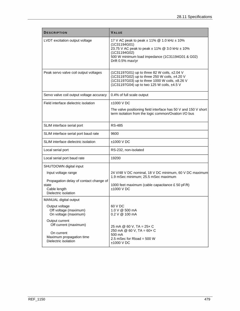
28.11 Specifications
REF_1150 479
DE S C RI P TI O N VALUE
LVDT excitation output voltage 17 V AC peak to peak ± 11% @ 1.0 kHz ± 10% (1C31194G01) 23.75 V AC peak to peak ± 11% @ 3.0 kHz ± 10% (1C31194G02) 500 W minimum load impedance (1C31194G01 & G02) Drift 0.5% max/yr
Peak servo valve coil output voltages (1C31197G01) up to three 82 W coils, ±2.04 V (1C31197G02) up to three 250 W coils, ±4.20 V (1C31197G03) up to three 1000 W coils, ±8.26 V (1C31197G04) up to two 125 W coils, ±4.5 V
Servo valve coil output voltage accuracy 0.4% of full scale output
Field interface dielectric isolation ±1000 V DC
The valve positioning field interface has 50 V and 150 V short term isolation from the logic common/Ovation I/O bus
SLIM interface serial port RS-485
SLIM interface serial port baud rate 9600
SLIM interface dielectric isolation ±1000 V DC
Local serial port RS-232, non-isolated
Local serial port baud rate 19200
SHUTDOWN digital input
Input voltage range Propagation delay of contact change of state Cable length Dielectric isolation
24 V/48 V DC nominal, 18 V DC minimum, 60 V DC maximum1.9 mSec minimum; 25.5 mSec maximum 1000 feet maximum (cable capacitance £ 50 pF/ft) ±1000 V DC
MANUAL digital output
Output voltage Off voltage (maximum) On voltage (maximum)
Output current Off current (maximum) On current Maximum propagation time Dielectric isolation
60 V DC 1.0 V @ 500 mA 0.2 V @ 100 mA 25 mA @ 60 V, TA = 25× C 250 mA @ 60 V, TA = 60× C 500 mA 2.5 mSec for Rload = 500 W ±1000 V DC
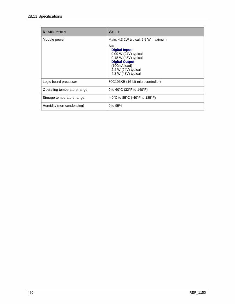
28.11 Specifications
480 REF_1150
DE S C RI P TI O N VALUE
Module power Main: 4.3 2W typical, 6.5 W maximum
Aux: Digital Input: 0.09 W (24V) typical 0.18 W (48V) typical Digital Output (100mA load) 2.4 W (24V) typical 4.8 W (48V) typical
Logic board processor 80C196KB (16-bit microcontroller)
Operating temperature range 0 to 60°C (32°F to 140°F)
Storage temperature range -40°C to 85°C (-40°F to 185°F)
Humidity (non-condensing) 0 to 95%

REF_1150 481
IN THIS SECTION
Description ......................................................................................................................481 Local I/O Features...........................................................................................................482 Controller Cabinet Components (Local I/O)....................................................................482 Extended I/O Cabinet Components ................................................................................486 Cabinet Components (Controller and Extended Cabinet) ..............................................488 General Requirements for I/O Cable ..............................................................................491 Local I/O Status LEDs.....................................................................................................491
29.1 DESCRIPTION
Note: Ovation local I/O is applicable for use in CE Mark certified systems except where noted.
The Ovation Distributed Control System provides modulating control, sequential control, and data acquisition for a variety of system applications. The local Ovation I/O consists of a mix of functional I/O units (modules) that communicate on the I/O bus to the Controller in the Controller's cabinet or in close proximity (9.1 meters (30 ft)).
Ovation I/O (see page 482) also provides for remote I/O functions.
Typically, the Ovation local I/O subsystem contains:
Controller cabinet with the redundant Ovation Controller, applicable I/O Interface Controller (see page 482) (IOIC) cards (PCQL or PCRL) power supplies, and I/O modules,
Extended I/O cabinet with additional I/O modules and power supplies (see page 486). Appropriate cable and connections (see page 491) between the cabinets (See Planning and
Designing Your Ovation System.) Interface support of existing Q-Line I/O using a PCQL card.
Note: Optional Ovation Marshalling cabinet configurations are also available, which provide for halfshell wiring terminations. (See Planning and Designing Your Ovation System.)
S E C T I O N 2 9
OVATION LOCAL I/O

29.2 Local I/O Features
482 REF_1150
29.2 LOCAL I/O FEATURES
The Ovation local I/O subsystem has the following features:
Maximum number of local I/O modules per PCRL: 64 (eight branches with eight modules each).
Maximum number of Local I/O modules per Controller: 128 (two PCRLs) Modular, “plug-in” components. Quick installation and configuration of the modules. DIN Rail mounting of the I/O base units. Unique base unit interconnection scheme eliminates power and communications wiring. Base unit common to all standard I/O modules and base units are available for Relay Output
modules.
29.3 CONTROLLER CABINET COMPONENTS (LOCAL I/O)
The Ovation I/O Controller cabinet (see page 484) contains the following:
Note: Refer to the appropriate Planning and Installing Your Ovation System manual for your system for additional cabinet and cable information.
Redundant Ovation Controller Chassis (see page 485) - Housing two separate Controllers. Each Controller contains:
Pentium PC Processor Board - To perform I/O control.
Power Supply Board - Converts +24V to +5V and ±12V to power all components of the Controller chassis.
Network Interface Card - Provides the interface between the Ovation Controller and other highway components of the system, FDDI/CDDI and Fast Ethernet versions are supported.
PCRL Board - PCI to local Ovation I/O interface board, used only if controlling local I/O modules (up to two PCRL cards per each Controller).
PCQL Board - PCI to local Q-Line interface board, used only if controlling local Q-Line I/O boards (up to two PCQL cards per each Controller). (Not applicable for CE Mark certified systems.) Refer to the appropriate Q-Line Installation Manual for your system for Q-Line I/O installation information.
29.3 Controller Cabinet Components (Local I/O)
REF_1150 483
Power Supply - DIN Rail Mounted. Generates +24V to power the electronics in the I/O Controller Cabinet, as well as +24V auxiliary power. Two are required for redundancy. An optional separate +48V auxiliary power supply is also available.
Power Distribution Module (see page 486) (5A26304) - Provides connectors for cables used to distribute +24V to the Redundant Controller Chassis, and +24V and auxiliary power to branches of local I/O.
Standard I/O Modules and Bases (see page 488) - Standard Ovation I/O modules which interface to field devices.
Relay Output Module and Bases (see page 491) - Relay module base, 1.5 times larger than a standard I/O base unit, containing electronics module and relays to control field devices (see page 491).
I/O Dual Branch Transition Panel (see page 491) (ROP - 4D33922) - Connects to two branches of I/O, providing a point to bring in +24V redundant power, auxiliary power, and the local I/O communications bus. Connections are provided on the I/O Transition Panel to daisy-chain the local I/O communications bus from one ROP to the next (up to eight I/O branches maximum may be daisy-chained together).
I/O Branch Terminator (1B30023) - Connects to the A or B-side of a standard I/O base at the end of a branch having no Attachment Unit Module to terminate the local I/O bus.
CAUTION! The I/O addressing for the Ovation database is determined from the positions of the bases installed in the cabinets.
We recommends that all possible bases (typically four) be installed in the right-most branch of each side of a cabinet, even if they are not all filled with I/O modules. This will prevent disruption of the database if additional I/O modules are installed in the future.
I/O modules should be installed in the right-most branch of each side of a cabinet from the BOTTOM UP. I/O modules should be installed in the left-most branch of each side of a cabinet from the TOP DOWN.
If Relay Output modules are mixed with Standard I/O modules on the same branch, the Standard I/O module base must always start in an odd-numbered position on the branch (positions 1/2, 3/4, 5/6, or 7/8).
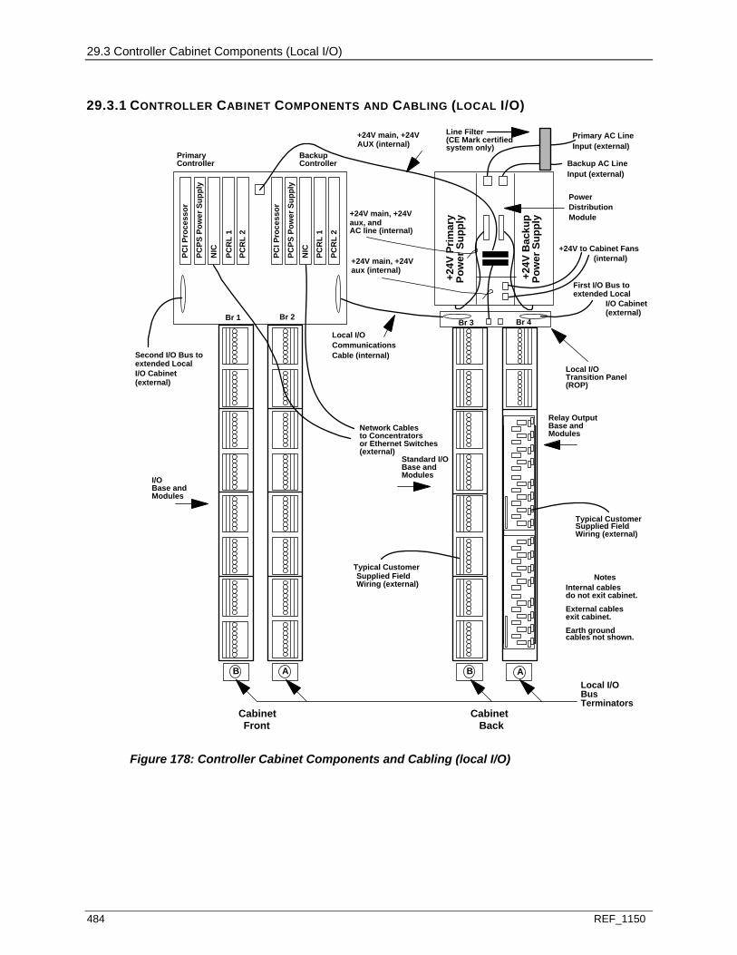
29.3 Controller Cabinet Components (Local I/O)
484 REF_1150
29.3.1 CONTROLLER CABINET COMPONENTS AND CABLING (LOCAL I/O)
+24V
Prim
ary
Pow
er S
uppl
y
+24V
Bac
kup
Pow
er S
uppl
y
Front Back
PowerDistributionModule
PCI P
roce
ssor
PCPS
Pow
er S
uppl
y
NIC
PCR
L 2
PCI P
roce
ssor
NIC
PCR
L 1
PCR
L 2
PrimaryController
BackupController
Cabinet Cabinet
Br 1 Br 2Br 3 Br 4
+24V main, +24V
Local I/OCommunicationsCable (internal)
I/OBase andModules
AUX (internal)
Local I/OBusTerminators
Primary AC LineInput (external)
Backup AC LineInput (external)
+24V to Cabinet Fans(internal)
extended LocalI/O Cabinet(external)
+24V main, +24V aux (internal)
+24V main, +24V aux, andAC line (internal)
Typical Customer
Relay OutputBase andModules
Network Cablesto Concentratorsor Ethernet Switches
NotesInternal cablesdo not exit cabinet.External cablesexit cabinet.Earth groundcables not shown.
Local I/OTransition Panel(ROP)
Line Filter(CE Mark certifiedsystem only)
ABA
Standard I/OBase andModules
Supplied FieldWiring (external)
Typical Customer
Supplied FieldWiring (external)
PCPS
Pow
er S
uppl
y
PCR
L 1
B
First I/O Bus to
extended LocalI/O Cabinet(external)
Second I/O Bus to
(external)
Figure 178: Controller Cabinet Components and Cabling (local I/O)
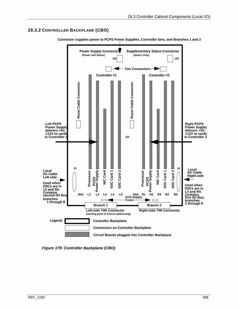
29.3 Controller Cabinet Components (Local I/O)
REF_1150 485
29.3.2 CONTROLLER BACKPLANE (CBO)
Proc
esso
r
Pow
er S
uppl
y
NIC
Car
d
IOIC
Car
d 1
IOIC
Car
d 2
Res
et C
able
Con
nect
or
Proc
esso
r
Pow
er S
uppl
y
NIC
Car
d
IOIC
Car
d 1
IOIC
Car
d 2
Res
et C
able
Con
nect
or
Power Supply Connector Supplementary Status Connector
Fan Connectors
Controller #1 Controller #2
Left-side TWI Connector Right-side TWI Connector
I/O CableLeft-side
I/O CableRight-side
Legend: Controller Backplane
Connectors on Controller Backplane
Circuit Boards plugged into Controller Backplane
Used whenIOICs are in L5 and R5.
1 through 8
Slot L1 L2 L3 L4 L5 Slot R1 R2 R3 R4 R5
Local Local
AUX SupplyFuses
J26J25
J3 J4
C
J25
(starting point of branch addressing)
(Power and Status) (Status Only)
Connector supplies power to PCPS Power Supplies, Controller fans, and Branches 1 and 2
PCPS
PCPS
Left PCPSPower Supply delivers +5V,±12V to cardsin Controller 1
Right PCPSPower Supply delivers +5V,±12V to cardsin Controller 2
Branch 1 Branch 2
Containssecond I/O Bus,branches
Used whenIOICs are in L4 and R4.
3 through 8
Containsfirst I/O Bus,branches
Figure 179: Controller Backplane (CBO)

29.4 Extended I/O Cabinet Components
486 REF_1150
29.4 EXTENDED I/O CABINET COMPONENTS
The Ovation I/O Extended cabinet contains the following:
Refer to the Planning and Installing Your Ovation System manual that is appropriate for your system for additional cabinet and cable information.
Power Supply - DIN Rail Mounted. Generates +24V and auxiliary power for the local I/O modules in the extended cabinet. Two are required for redundancy.
Power Distribution Module (5A26304) - Provides connectors for cables used to distribute power to branches of local I/O.
Standard I/O Modules and Base - Standard Ovation I/O modules which interface to field devices.
Relay Output Module and Bases - Relay module base, 1.5 times larger than a standard I/O base unit, containing electronics module and relays to control field devices.
I/O Dual Branch Transition Panel (ROP - 4D33922) - Connects to two branches of I/O, providing a point to bring in +24V redundant power, auxiliary supplies, and the local I/O communications bus. Connections are provided on the I/O Transition Panel to daisy-chain the local I/O communications bus from one ROP to the next (up to eight I/O branches maximum may be daisy-chained together).

29.4 Extended I/O Cabinet Components
REF_1150 487
I/O Single Branch Transition Panels (Top - RRP 3A99252; Bottom - RRB 3A99253) - Used with Relay Output modules for a single I/O branch of up to eight relay bases. Supplies +24V redundant power, auxiliary power, and local communications bus to the branch. Mounted at the top/bottom of the extended cabinet. Only ONE I/O branch is used and remaining branches are passed on.
Prim
ary
Pow
er S
uppl
y
Bac
kup
Pow
er S
uppl
y
Front Back
PowerDistributionModule
Cabinet Cabinet
+24V main, +24V
Local I/OCommunicationsCable (internal)
I/OBase andModules
AUX (internal)
Local I/OBusTerminators
Backup AC/DC LineInput (external)
+24V to Cabinet Fans(internal)
To extended LocalI/O Cabinet
(external) Br "n+4"
+24V main, +24V AUX (internal)
+24V main, +24V AUX, andAC/DC line (internal)
Typical CustomerSupplied FieldWiring (external)
I/OBase andModules
NotesInternal cablesdo not exit cabinet.
External cablesexit cabinet.
Earth groundcables not shown.
Local I/OTransition Panel(ROP)Local I/O
Transition Panel(ROP)
Local I/O CommunicationsCable from Controller or Cabinet (external) Br "n-1"
Line Filter(CE Mark certifiedsystem only)
Primary AC/DC Line *Input (external)
* DC Power Supplies are not applicable to CE Mark Certified systems.
Br "n" Br "n + 1" Br "n + 2" Br "n + 3"
Figure 180: Ovation Extended I/O Cabinet (illustrating cables and Standard I/O)
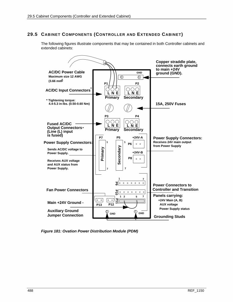
29.5 Cabinet Components (Controller and Extended Cabinet)
488 REF_1150
29.5 CABINET COMPONENTS (CONTROLLER AND EXTENDED CABINET)
The following figures illustrate components that may be contained in both Controller cabinets and extended cabinets:
L N E
L N EL N E
Primary
Primary
Secondary
Secondary
Prim
ary
Seco
ndar
y
+24V-A
+24V-B
AC/DC Power Cable
AC/DC Input Connectors
15A, 250V Fuses
Fused AC/DCOutput Connectors
Power Supply Connectors:Receives 24V main outputfrom Power Supply
Power Supply Connectors:Sends AC/DC voltage to Power Supply.
Receives AUX voltageand AUX status fromPower Supply.
Fan Power ConnectorsPower Connectors to Controller and Transition
+24V Main (A, B) AUX voltage
Power Supply status
P1 P2
Maximum size 12 AWG(3.66 mm2)
Jumper Connection
Panels carrying:
P9P10
P11Main +24V Ground -
Auxiliary Ground
(Line (L) input is fused)
P3 P4
P13
P7 P5
P6
P8
P12
L N E
GND
GNDGNDGrounding Studs
Copper straddle plate,connects earth groundto main +24V ground (GND).
1 7
1 2 5 7
1 1
7 7
*
* Tightening torque:4.4-5.3 in-lbs. (0.50-0.60 Nm)
*
Figure 181: Ovation Power Distribution Module (PDM)
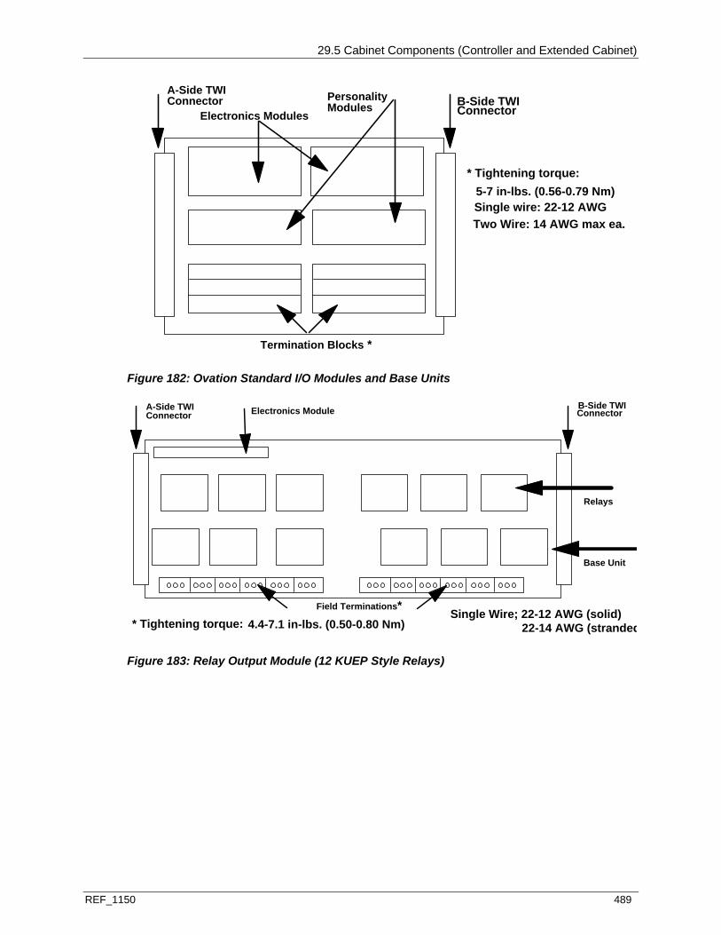
29.5 Cabinet Components (Controller and Extended Cabinet)
REF_1150 489
A-Side TWIConnector B-Side TWI
ConnectorElectronics Modules
Termination Blocks
PersonalityModules
* Tightening torque:5-7 in-lbs. (0.56-0.79 Nm)Single wire: 22-12 AWGTwo Wire: 14 AWG max ea.
*
Figure 182: Ovation Standard I/O Modules and Base Units
B-Side TWIConnectorElectronics Module
Field Terminations
Relays
A-Side TWIConnector
Base Unit
* Tightening torque:*
4.4-7.1 in-lbs. (0.50-0.80 Nm)Single Wire; 22-12 AWG (solid)
22-14 AWG (stranded
Figure 183: Relay Output Module (12 KUEP Style Relays)
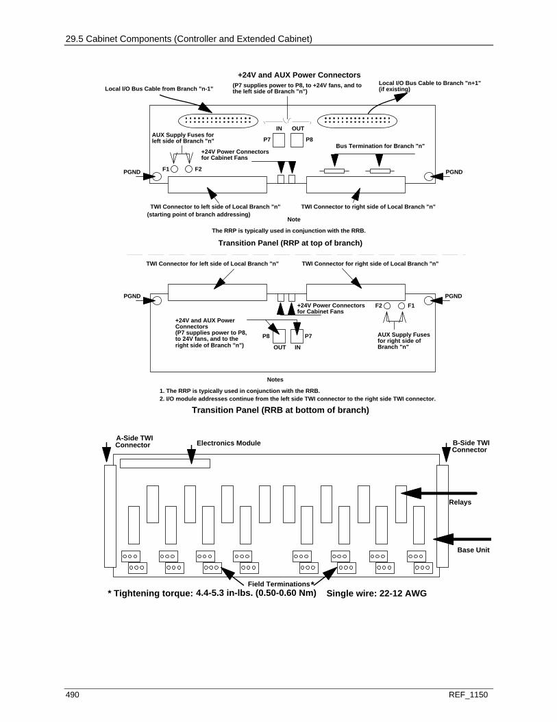
29.5 Cabinet Components (Controller and Extended Cabinet)
490 REF_1150
Local I/O Bus Cable from Branch "n-1"Local I/O Bus Cable to Branch "n+1"
+24V Power Connectorsfor Cabinet Fans
IN OUT
P7 P8
(if existing)
+24V and AUX Power Connectors(P7 supplies power to P8, to +24V fans, and to
F1 F2 PGNDPGND
AUX Supply Fuses for
TWI Connector to left side of Local Branch "n" TWI Connector to right side of Local Branch "n"
left side of Branch "n"
Note
The RRP is typically used in conjunction with the RRB.
Bus Termination for Branch "n"
the left side of Branch "n")
(starting point of branch addressing)
OUT IN
TWI Connector for left side of Local Branch "n" TWI Connector for right side of Local Branch "n"
AUX Supply Fusesfor right side ofBranch "n"
F2 F1PGND PGND
P8 P7
+24V and AUX PowerConnectors(P7 supplies power to P8,
right side of Branch "n")
Notes
1. The RRP is typically used in conjunction with the RRB.2. I/O module addresses continue from the left side TWI connector to the right side TWI connector.
+24V Power Connectorsfor Cabinet Fans
to 24V fans, and to the
Transition Panel (RRP at top of branch)
Transition Panel (RRB at bottom of branch)
Electronics Module
Field Terminations
Relays
A-Side TWIConnector B-Side TWI
Connector
Base Unit
* Tightening torque:*
4.4-5.3 in-lbs. (0.50-0.60 Nm) Single wire: 22-12 AWG
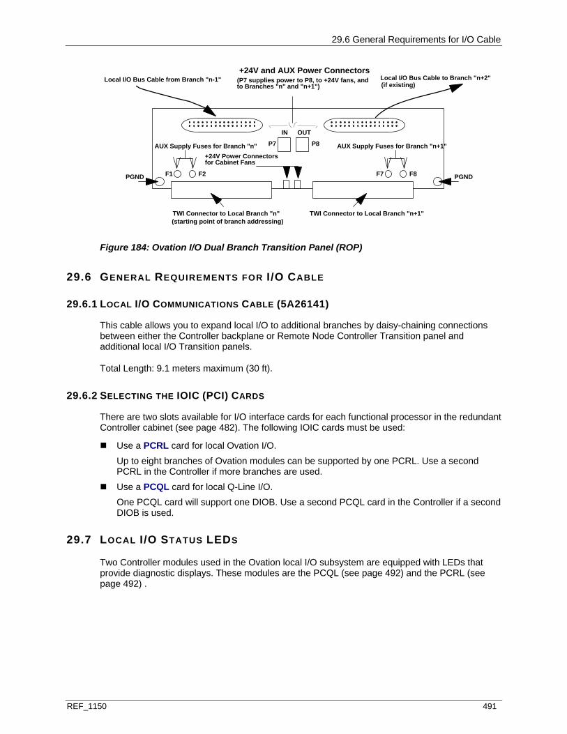
29.6 General Requirements for I/O Cable
REF_1150 491
Local I/O Bus Cable from Branch "n-1" Local I/O Bus Cable to Branch "n+2"
+24V Power Connectorsfor Cabinet Fans
IN OUT
AUX Supply Fuses for Branch "n+1"P7 P8
(if existing)
+24V and AUX Power Connectors(P7 supplies power to P8, to +24V fans, and
F1 F2 F7 F8 PGNDPGND
AUX Supply Fuses for Branch "n"
TWI Connector to Local Branch "n" TWI Connector to Local Branch "n+1"
to Branches "n" and "n+1")
(starting point of branch addressing)
Figure 184: Ovation I/O Dual Branch Transition Panel (ROP)
29.6 GENERAL REQUIREMENTS FOR I/O CABLE
29.6.1 LOCAL I/O COMMUNICATIONS CABLE (5A26141)
This cable allows you to expand local I/O to additional branches by daisy-chaining connections between either the Controller backplane or Remote Node Controller Transition panel and additional local I/O Transition panels.
Total Length: 9.1 meters maximum (30 ft).
29.6.2 SELECTING THE IOIC (PCI) CARDS
There are two slots available for I/O interface cards for each functional processor in the redundant Controller cabinet (see page 482). The following IOIC cards must be used:
Use a PCRL card for local Ovation I/O. Up to eight branches of Ovation modules can be supported by one PCRL. Use a second PCRL in the Controller if more branches are used.
Use a PCQL card for local Q-Line I/O. One PCQL card will support one DIOB. Use a second PCQL card in the Controller if a second DIOB is used.
29.7 LOCAL I/O STATUS LEDS
Two Controller modules used in the Ovation local I/O subsystem are equipped with LEDs that provide diagnostic displays. These modules are the PCQL (see page 492) and the PCRL (see page 492) .
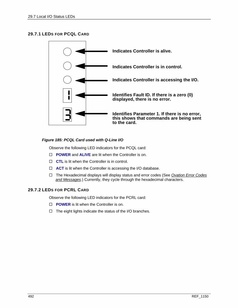
29.7 Local I/O Status LEDs
492 REF_1150
29.7.1 LEDS FOR PCQL CARD
Indicates Controller is alive.
Identifies Fault ID. If there is a zero (0)
Indicates Controller is in control.
Indicates Controller is accessing the I/O.
Identifies Parameter 1. If there is no error,
displayed, there is no error.
this shows that commands are being sentto the card.
Figure 185: PCQL Card used with Q-Line I/O
Observe the following LED indicators for the PCQL card:
POWER and ALIVE are lit when the Controller is on.
CTL is lit when the Controller is in control.
ACT is lit when the Controller is accessing the I/O database.
The Hexadecimal displays will display status and error codes (See Ovation Error Codes and Messages.) Currently, they cycle through the hexadecimal characters.
29.7.2 LEDS FOR PCRL CARD
Observe the following LED indicators for the PCRL card:
POWER is lit when the Controller is on.
The eight lights indicate the status of the I/O branches.
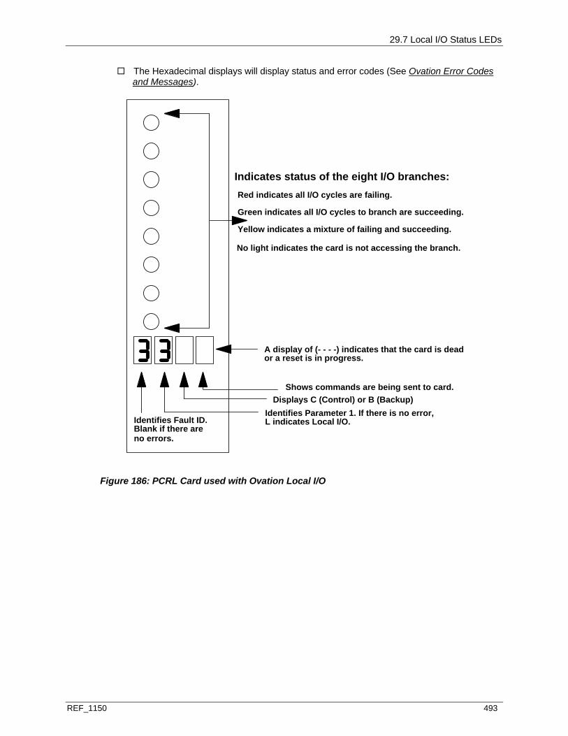
29.7 Local I/O Status LEDs
REF_1150 493
The Hexadecimal displays will display status and error codes (See Ovation Error Codes and Messages).
Indicates status of the eight I/O branches:
Identifies Parameter 1. If there is no error,
Red indicates all I/O cycles are failing.
Green indicates all I/O cycles to branch are succeeding.
Yellow indicates a mixture of failing and succeeding.
No light indicates the card is not accessing the branch.
L indicates Local I/O.Identifies Fault ID. Blank if there are
Displays C (Control) or B (Backup)Shows commands are being sent to card.
A display of (- - - -) indicates that the card is deador a reset is in progress.
no errors.
Figure 186: PCRL Card used with Ovation Local I/O

REF_1150 495
IN THIS SECTION
Description ......................................................................................................................495 Remote I/O Features.......................................................................................................496 Controller Cabinet Components (Remote I/O)................................................................496 Remote Node Cabinet Components ...............................................................................503 Extended I/O Cabinet Components ................................................................................507 General Requirements for I/O Cable ..............................................................................513 Configuring Remote I/O Cabinets ...................................................................................514 Diagnostic LEDs..............................................................................................................518
30.1 DESCRIPTION
Note: Ovation remote I/O is applicable for use in CE Mark certified systems except where noted.
The Ovation Distributed Control System provides modulating control, sequential control, and data acquisition for a variety of system applications. Although using local I/O (see page 481) is typically the most practical control solution, a remote process might need to be controlled.
Remote I/O is typically used where a process requires that I/O modules be located near the process, even though the Controller is not. The remote I/O modules are connected to the Controller through long distance, serial media, such as fiber-optic cables.
Typically, the Ovation remote I/O subsystem contains:
Controller cabinet (see page 496) containing the redundant Ovation Controller, applicable I/O Interface Controller (IOIC) cards (PCRR), power supplies, and I/O modules.
Remote Node cabinet(s) (see page 503) containing the redundant Remote Node Controller module, as well as I/O cards.
Extended I/O cabinet (see page 507) containing additional I/O modules and power supplies. Appropriate cable (see page 513) and connections between cabinets (See Planning and
Designing Your Ovation System.)
Note: An optional Ovation Marshalling cabinet is also available. The rear of this 32 inch wide cabinet provides for halfshell wiring terminations, but has the same mechanical and electrical performance as the standard Ovation cabinet. (See Planning and Designing Your Ovation System.)
S E C T I O N 3 0
OVATION REMOTE I/O

30.2 Remote I/O Features
496 REF_1150
30.2 REMOTE I/O FEATURES
The Ovation remote I/O subsystem has the following features:
Maximum number of Remote Nodes: 16 nodes, redundantly controlled (eight nodes for each PCRR card).
Maximum number of I/O modules per remote node: 641 (eight branches with eight modules for each branch).
Maximum number of I/O modules per PCRR card: 5121 (eight nodes, eight branches for each node, eight modules for each branch).
Maximum number of I/O modules per Controller: 10241. Remote I/O Bus configuration: 10 BASE-FL Ethernet physical layer with a proprietary
protocol. Remote I/O cycle time: <100m sec (typical), double byte word access as seen by PCRR. Standard Remote communications media offered: Fiber-optic Maximum cable length (see page 496) for 850 nm fiber-optic media: 2 km (without
repeaters)2. Maximum cable length (see page 496) for 1300 nm fiber-optic media: 4 km. Distances of 6 km can be achieved with repeaters (up to two repeaters) (Not applicable for
CE Mark certified systems.).2 Remote communication diagnostics can be performed in the Primary and Backup system
without affecting I/O modules. The diagnostics available are: 1. Simulation of all types of bus cycles (such as local I/O including statuses, bit corruption, message length faults, collision faults, and no response).
2. Loopback of all messages from PCRR through the MAU.
3. Connection check of AUI cable and remote node link. Status LEDs: Available on PCRR, MAU, and RNC modules. Interface support of existing Q-Line I/O using Q-Line QOR card.
1 These numbers represent hardware capabilities. Controller software limitations are not implied.
2 Repeaters are third-party Ethernet devices that must be endorsed by Emerson design engineers.
30.3 CONTROLLER CABINET COMPONENTS (REMOTE I/O)
The Ovation Remote I/O Controller cabinet (see page 499) contains the following:
Redundant Controller Chassis (see page 500) - This rack in the Controller cabinet provides the backplane for two separate Controllers. For each Controller, the backplane interconnects the following components:
Pentium PC Processor Board - Third party functional processor for the Controller.
Power Supply Board Kit - Contains a PCPS power supply converting +24V to +5V and ±12V to power all components in the Controller chassis.

30.3 Controller Cabinet Components (Remote I/O)
REF_1150 497
Network Interface Card (NIC) - Provides the interface between the Ovation Controller, and the other highway components of the system. FDDI/CDDI and Fast Ethernet versions are supported.
PCRR Board - IOIC (PCI) to remote Ovation or Q-Line I/O interface board, serving as the master of the remote I/O bus. Refer to the “Q-Line Installation Manual” for remote Q-Line I/O installation information (only 850 nm optics, with 2 km maximum length, are available for remote Q-Line applications).
A PCRR board has two Attachment Unit Interface (AUI) ports each of which may connect to an Attachment Unit Module using an AUI cable. Together, the two ports typically serve as the primary I/O bus master with another PCRR card providing the redundant pair (up to two PCRR cards per each Controller).
Power Supply - DIN Rail Mounted. Generates +24V to power the electronics in the I/O Controller Cabinet, as well as +24V auxiliary power. Two are required for redundancy. An optional separate +48V auxiliary power supply is also available.
Power Distribution Module (see page 509) (5A26304) - Provides connectors for cables used to distribute +24V to the Redundant Controller Chassis, and +24V and auxiliary power to branches of local I/O.
Standard I/O Modules and Bases (see page 510) - Standard Ovation I/O modules which interface to field devices.
Relay Output Module and Bases (see page 511) - Relay module base, 1.5 times larger than a standard I/O base unit, containing electronics module and relays to control field devices).
I/O Dual Branch Transition Panel (see page 512) (ROP - 4D33922) - Connects to two branches of I/O, providing a point to bring in +24V redundant power, auxiliary power, and the local I/O communications bus. Connections are provided on the I/O Transition Panel to daisy-chain the local I/O communications bus from one ROP to the next (up to eight I/O branches maximum may be daisy-chained together).
30.3 Controller Cabinet Components (Remote I/O)
498 REF_1150
I/O Branch Terminator (see page 513) (1B30023) - Connects to the A or B-side of a standard I/O base at the end of a branch having no Attachment Unit Module to terminate the local I/O bus.
CAUTION! The I/O addressing for the Ovation database is determined from the positions of the bases installed in the cabinets.
We recommends that all possible bases (typically four) be installed in the right-most branch of each side of a cabinet, even if they are not all filled with I/O modules. This will prevent disruption of the database if additional I/O modules are installed in the future.
I/O modules should be installed in the right-most branch of each side of a cabinet from the BOTTOM UP. I/O modules should be installed in the left-most branch of each side of a cabinet from the TOP DOWN.
If Relay Output modules are mixed with Standard I/O modules on the same branch, the Standard I/O module base must always start in an odd-numbered position on the branch (positions 1/2, 3/4, 5/6, or 7/8).
Media Attachment Unit (see page 501) (MAU) - This module provides a point of attachment for fiber optic cables used to transfer messages over long distances between the PCRR and up to four remote nodes (see page 502). The module directs messages between the PCRR and one of the four remote nodes at a time as selected, converting signals readable by the PCRR to signals compatible with the fiber optic media and vise versa. The following components comprise the MAU:
Electronics Module (1C31179) - Houses the Attachment Unit Logic Board (LAU) which provides power for the module and displays LED indication that the fiber optic cables are connected and the Remote Node Controller Module has power.
Personality Module (1C31181) - Houses the Attachment Unit Personality Board (PAU) which translates signals between the PCRR and the fiber optic media and provides connectors for the fiber optic cables.
MAU Subsystem
EL E CT RO NI C MO D U LE
PE R S O N AL I T Y MO D U LE
LE NG T H O F OP TI C AL L I NK1 CH AN N E L S OP TI CS
2
1C31179G01 1C31181G01 Up to 2 kilometers (6,560 ft) 2 850 nm
1C31179G02 1C31181G02 Up to 2 kilometers (6,560 ft) 4 850 nm
1C31179G01 1C31181G03 Up to 4 kilometers (13,120 ft) 2 1300 nm
1C31179G02 1C31181G04 Up to 4 kilometers (13,120 ft) 4 1300 nm
1 In order not to be required to select extended PCRR time-out periods, it is recommended that you do NOT exceed an optical length of 3.7 km. 2 An Ovation Controller cabinet MAU MUST use the same type of optics (850 nm or 1300 nm) for each of the remote nodes that it interfaces. An MAU cannot interface both 850 nm remote nodes (using 1C1204G01 Personality modules) and 1300 nm remote nodes (using 1C31204G03 Personality modules.)
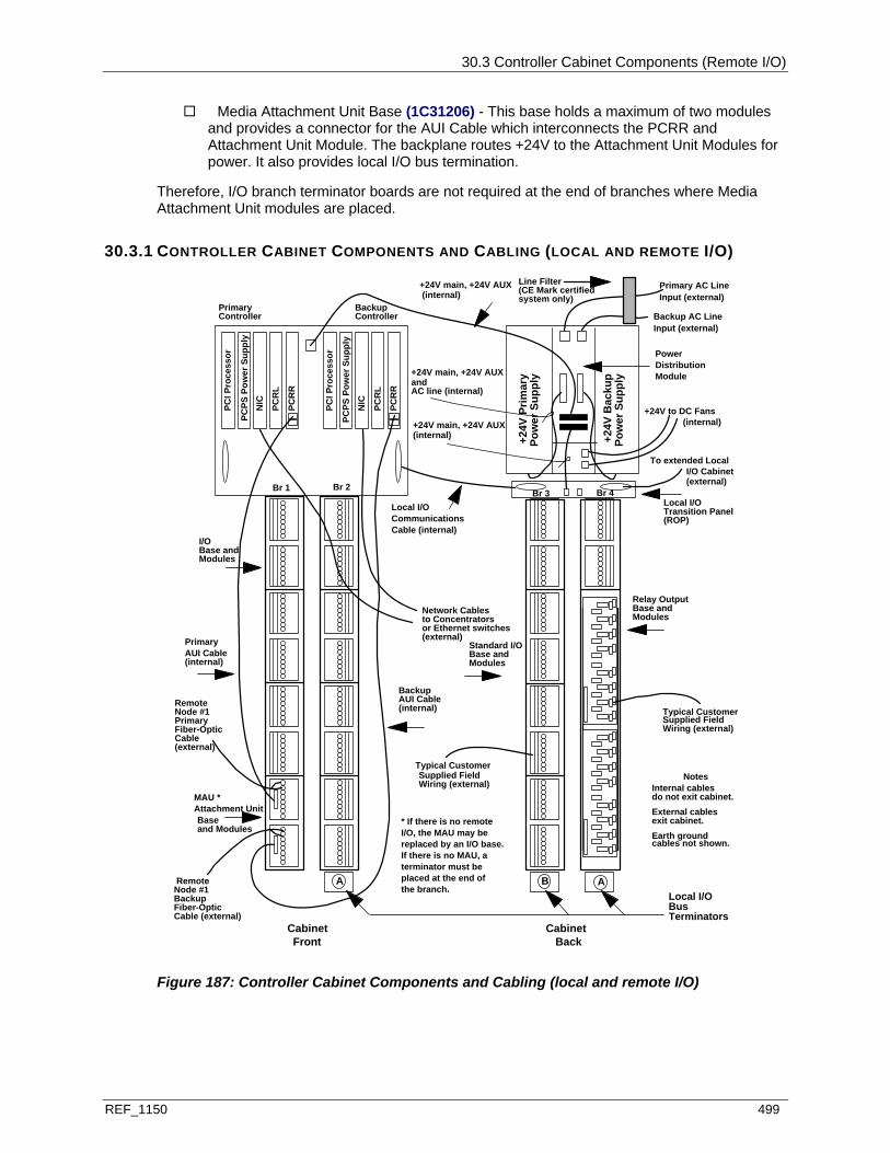
30.3 Controller Cabinet Components (Remote I/O)
REF_1150 499
Media Attachment Unit Base (1C31206) - This base holds a maximum of two modules and provides a connector for the AUI Cable which interconnects the PCRR and Attachment Unit Module. The backplane routes +24V to the Attachment Unit Modules for power. It also provides local I/O bus termination.
Therefore, I/O branch terminator boards are not required at the end of branches where Media Attachment Unit modules are placed.
30.3.1 CONTROLLER CABINET COMPONENTS AND CABLING (LOCAL AND REMOTE I/O)
+24V
Prim
ary
Pow
er S
uppl
y
+24V
Bac
kup
Pow
er S
uppl
y
Front Back
PowerDistributionModule
MAU * Attachment Unit
PCI P
roce
ssor
PCPS
Pow
er S
uppl
yN
IC
PCR
L
PCR
R
PCI P
roce
ssor
NIC
PCR
L
PCR
R
PrimaryController
BackupController
Cabinet Cabinet
Br 1 Br 2Br 3 Br 4
+24V main, +24V AUX
Local I/OCommunicationsCable (internal)
PrimaryAUI Cable
BackupAUI Cable
Baseand Modules
RemoteNode #1PrimaryFiber-OpticCable
RemoteNode #1BackupFiber-OpticCable (external)
I/OBase andModules
(internal)
Local I/OBusTerminators
Primary AC LineInput (external)
Backup AC LineInput (external)
+24V to DC Fans(internal)
To extended LocalI/O Cabinet(external)
+24V main, +24V AUX (internal)
+24V main, +24V AUX andAC line (internal)
(internal) Typical Customer
(external)
Relay OutputBase andModules
(internal)
Network Cablesto Concentratorsor Ethernet switches
NotesInternal cablesdo not exit cabinet.External cablesexit cabinet.Earth groundcables not shown.
Local I/OTransition Panel(ROP)
Line Filter(CE Mark certifiedsystem only)
* If there is no remoteI/O, the MAU may bereplaced by an I/O base.If there is no MAU, aterminator must beplaced at the end ofthe branch.
ABA
Standard I/OBase andModules
Supplied FieldWiring (external)
Typical Customer
Supplied FieldWiring (external)
PCPS
Pow
er S
uppl
y
(external)
Figure 187: Controller Cabinet Components and Cabling (local and remote I/O)
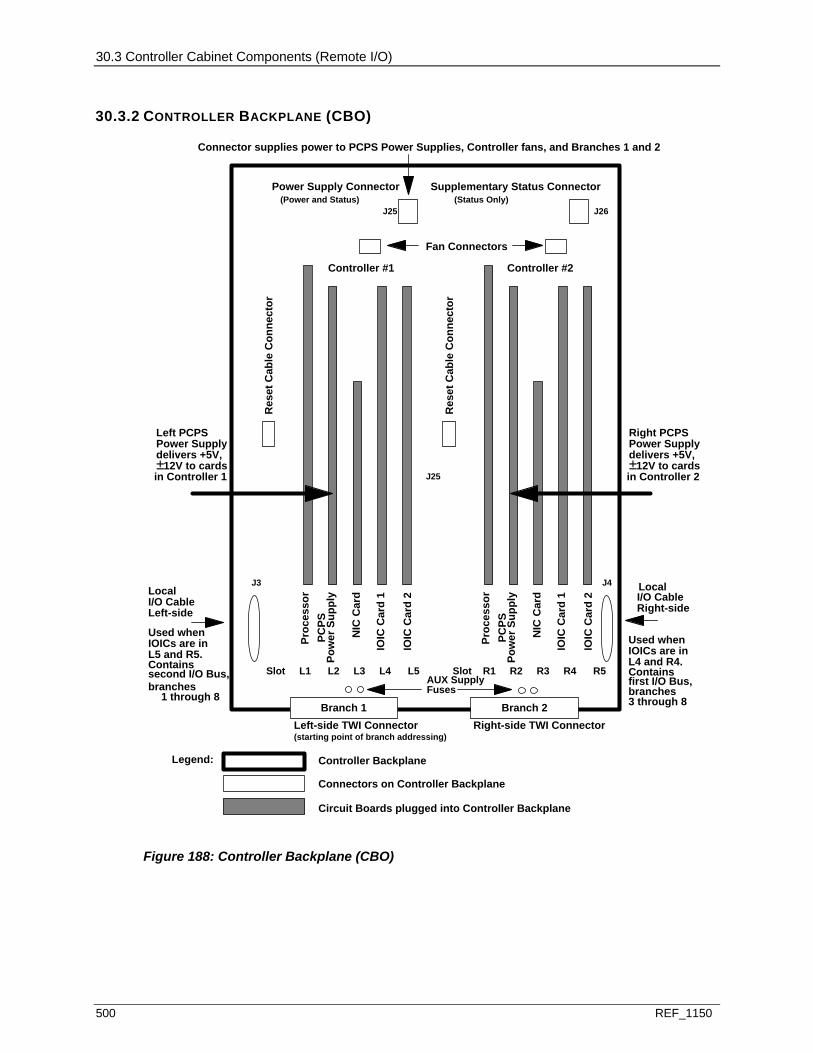
30.3 Controller Cabinet Components (Remote I/O)
500 REF_1150
30.3.2 CONTROLLER BACKPLANE (CBO)
Proc
esso
r
Pow
er S
uppl
y
NIC
Car
d
IOIC
Car
d 1
IOIC
Car
d 2
Res
et C
able
Con
nect
or
Proc
esso
r
Pow
er S
uppl
y
NIC
Car
d
IOIC
Car
d 1
IOIC
Car
d 2
Res
et C
able
Con
nect
or
Power Supply Connector Supplementary Status Connector
Fan Connectors
Controller #1 Controller #2
Left-side TWI Connector Right-side TWI Connector
I/O CableLeft-side
I/O CableRight-side
Legend: Controller Backplane
Connectors on Controller Backplane
Circuit Boards plugged into Controller Backplane
Used whenIOICs are in L5 and R5.
1 through 8
Slot L1 L2 L3 L4 L5 Slot R1 R2 R3 R4 R5
Local Local
AUX SupplyFuses
J26J25
J3 J4
C
J25
(starting point of branch addressing)
(Power and Status) (Status Only)
Connector supplies power to PCPS Power Supplies, Controller fans, and Branches 1 and 2
PCPS
PCPS
Left PCPSPower Supply delivers +5V,±12V to cardsin Controller 1
Right PCPSPower Supply delivers +5V,±12V to cardsin Controller 2
Branch 1 Branch 2
Containssecond I/O Bus,branches
Used whenIOICs are in L4 and R4.
3 through 8
Containsfirst I/O Bus,branches
Figure 188: Controller Backplane (CBO)
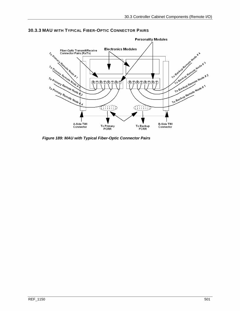
30.3 Controller Cabinet Components (Remote I/O)
REF_1150 501
30.3.3 MAU WITH TYPICAL FIBER-OPTIC CONNECTOR PAIRS
Figure 189: MAU with Typical Fiber-Optic Connector Pairs

30.3 Controller Cabinet Components (Remote I/O)
502 REF_1150
30.3.4 EXAMPLE OF TYPICAL MAU CABLE CONNECTIONS TO REMOTE NODES
+24V
Prim
ary
Pow
er S
uppl
y
+24V
Bac
kup
Pow
er S
uppl
y
PCI P
roce
ssor
PCPS
Pow
er S
uppl
y
NIC
PCR
R
PCR
R
PCI P
roce
ssor
NIC
PCR
R
PCR
R
PrimaryController
BackupController
Br 1 Br 2Br 3 Br 4
+24V
Prim
ary
Po
wer
Sup
ply
+24V
Bac
kup
Pow
er S
uppl
y
Controller Cabinet(front and back)
Remote Node #3(front and back)
MAU
LocalComm.Cable
PCPS
Pow
er S
uppl
y
+24V
Prim
ary
Pow
er S
uppl
y
+24V
Bac
kup
Pow
er S
uppl
y
Remote Node #4(front and back)
+24V
Prim
ary
Pow
er S
uppl
y
+24V
Bac
kup
Pow
er S
uppl
y
Remote Node #2(front and back)
+24V
Prim
ary
Pow
er S
uppl
y
+24V
Bac
kup
Pow
er S
uppl
y
Remote Node #1(front and back)
RNC RNC RNC
RNC
Figure 190: Example of Typical MAU Cable Connections to Remote Nodes
30.4 Remote Node Cabinet Components
REF_1150 503
30.4 REMOTE NODE CABINET COMPONENTS
The Ovation Remote Node (see page 505) cabinet, located remotely from the Controller cabinet contains the following:
Power Supply - DIN Rail Mounted. Generates +24V to power the electronics in the Remote Node Cabinet, as well as +24V auxiliary power. Two are required for redundancy.
Remote Node Controller (RNC) Module (see page 506) - Provides a point of attachment for remote I/O media used to transfer messages between the remote node and the MAU. There are only two Remote Node Controller Modules per remote node (one primary, one backup), regardless of the number of cabinets at the node. The module translates messages from the remote I/O bus into local I/O bus cycles that can be directed to as many as eight branches of local I/O modules. The following components comprise the Remote Node Controller Module:
Remote Node Electronics Module (1C31203) - Prepares messages received from the remote I/O Controller for the local I/O modules at the remote node. When an I/O module responds to the message, the module prepares the response to be sent back to the Controller over the fiber-optic media.
Remote Node Personality Module (1C31204G01 for 850 nm optics/1C31204G03 for 1300 nm optics) - Houses the Remote Node Personality Board (PAU) which provides connectors for the media used to transmit and receive remote messages between the Controller and remote node. Group 1 modules provide fiber-optic connections; (future plans are that group 2 modules provide an AUI port used to connect to third party transceivers). Power supply monitoring circuitry of the +24V redundant supplies is located on this module and is reported back to the electronics module to flag failure of the primary or backup supply.
Remote Node Controller Base (1C31205) - This unique base holds a maximum of two Remote Node Modules and interfaces directly to two I/O branches. It provides a rotary switch for node addressing and a D-connector for interfacing to as many as six additional I/O branches using a local I/O communications cable. The RNC base unit is connected to the Remote Node Transition Panel described below.
Remote Node Transition Panel (see page 506) (TND - 4D33924) - Interconnects the RNC base, Remote Power Supply Module (if used), and the branches of local I/O in a single Remote Node cabinet. The Remote Node Transition Panel (TND) also provides connectors for DIN Rail Mounted +24V Supplies or auxiliary supplies to be wired into the remote node.
Power Distribution Module (see page 509) (PDM - 5A26304) - Provides connectors for cables used to distribute +24V to the Redundant RNC, and +24V and auxiliary power to the branches of I/O.
Standard I/O Modules and Base (see page 510) - Standard Ovation I/O modules which interface to remote field devices when placed in the Remote Node cabinet.
Relay Output Module and Base (see page 511) - Relay Output I/O modules which interface to remote field devices when placed in the Remote Node cabinet.
I/O Dual Branch Transition Panel (see page 512) (ROP - 4D33922) - Connects to two branches of I/O, providing a point to bring in +24V redundant power, auxiliary power, and the local I/O communications bus. Connections are provided on the I/O Transition Panel to daisy-chain the local I/O communications bus from one ROP to the next (up to eight I/O branches maximum may be daisy-chained (see page 516) together.

30.4 Remote Node Cabinet Components
504 REF_1150
I/O Single Branch Transition Panels (see page 513) (Top - RRP 3A99252; Bottom - RRB 3A99253) - Used with Relay Output modules for a single I/O branch of up to eight relay bases. Supplies +24V redundant power, auxiliary power, and local communications bus to the branch. Mounted at the top/bottom of the extended cabinet (see page 513). Only one I/O branch is used and branches 2 through 8 are passed on.
I/O Branch Terminator Board A or B (1B30023) - Connects to the A/B-side of a standard I/O base (see page 505) at the end of a branch to terminate the I/O bus.

30.4 Remote Node Cabinet Components
REF_1150 505
30.4.1 TYPICAL REMOTE NODE CABINET
+24V
Prim
ary
Terminator Board
ROP
Pow
er S
uppl
y
+24V
Bac
kup
Pow
er S
uppl
y
Back
PowerDistributionModule
Terminator Board
Cabinet
Br 1 Br 2Br 3 Br 4
To Branches 5,6,7,8
B-Side A-Side
Power Cable
Local I/OCommunicationsCable
I/OBase andModules
Terminator BoardTerminator Board B-Side A-Side
TND
Remote Node Controller (RNC)Base and Modules
PrimaryFiber-OpticCable
BackupFiber-OpticCable
FrontCabinet
Primary AC LineInput (external)
Backup AC LineInput (external)
Line Filter(CE Mark certifiedsystem only)
Figure 191: Typical Remote Node Cabinet
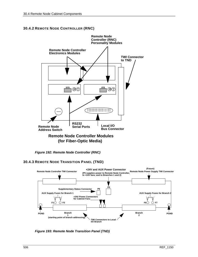
30.4 Remote Node Cabinet Components
506 REF_1150
30.4.2 REMOTE NODE CONTROLLER (RNC)
R T R T
Remote Node Controller Modules(for Fiber-Optic Media)
Electronics ModulesRemote Node Controller
Controller (RNC) Personality Modules
Remote Node
Remote NodeAddress Switch
RS232Serial Ports
TWI Connectorto TND
Local I/OBus Connector
Figure 192: Remote Node Controller (RNC)
30.4.3 REMOTE NODE TRANSITION PANEL (TND)
+24V Power Connectorsfor Cabinet Fans
Remote Node Controller TWI Connector Remote Node Power Supply TWI Connector
TWI Connectors to LocalI/O Branch
Supplementary Status Connector
(Future)
Branch1
Branch2
P6
PGND PGND
P5
F1 F2 F6 F7
AUX Supply Fuses for Branch 1 AUX Supply Fuses for Branch 2
+24V and AUX Power Connector(P5 supplies power to Remote Node Controller,to +24V fans, and to Branches 1 and 2)
(starting point of branch addressing)
Figure 193: Remote Node Transition Panel (TND)

30.5 Extended I/O Cabinet Components
REF_1150 507
30.5 EXTENDED I/O CABINET COMPONENTS
The Ovation I/O Extended cabinet contains the following:
Note: Refer to the Planning and Installing Your Ovation System manual that is appropriate for your system for additional cabinet and cable information.
Power Supply - DIN Rail Mounted. Generates +24V to power the electronics in the Remote I/O Controller Cabinet, as well as +24V auxiliary power. Two are required for redundancy.
Power Distribution Module (see page 509) (5A26304) - Provides connectors for cables used to distribute +24V to the Redundant RNC and to branches of local I/O.
Standard I/O Modules and Base (see page 510) - Standard Ovation I/O modules which interface to field devices.
Relay Output Module and Base (see page 511) - Relay module base, 1.5 times larger than a standard I/O base unit, containing electronics module and relays to control field devices.
I/O Dual Branch Transition Panel (see page 512) (ROP - 4D33922) - Connects to two branches of I/O, providing a point to bring in +24V redundant power, auxiliary supplies, and the local I/O communications bus. Connections are provided on the I/O Transition Panel to daisy-chain the local I/O communications bus from one ROP to the next (up to eight I/O branches maximum may be daisy-chained together).
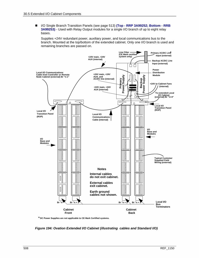
30.5 Extended I/O Cabinet Components
508 REF_1150
I/O Single Branch Transition Panels (see page 513) (Top - RRP 3A99252; Bottom - RRB 3A99253) - Used with Relay Output modules for a single I/O branch of up to eight relay bases. Supplies +24V redundant power, auxiliary power, and local communications bus to the branch. Mounted at the top/bottom of the extended cabinet. Only one I/O branch is used and remaining branches are passed on.
Prim
ary
Pow
er S
uppl
y
Bac
kup
Pow
er S
uppl
y
Front Back
PowerDistributionModule
Cabinet Cabinet
+24V main, +24V
Local I/OCommunicationsCable (internal)
I/OBase andModules
AUX (internal)
Local I/OBusTerminators
Backup AC/DC LineInput (external)
+24V to Cabinet Fans(internal)
To extended LocalI/O Cabinet
(external) Br "n+4"
+24V main, +24V AUX (internal)
+24V main, +24V AUX, andAC/DC line (internal)
Typical CustomerSupplied FieldWiring (external)
I/OBase andModules
NotesInternal cablesdo not exit cabinet.
External cablesexit cabinet.
Earth groundcables not shown.
Local I/OTransition Panel(ROP)Local I/O
Transition Panel(ROP)
Local I/O CommunicationsCable from Controller or RemoteNode Cabinet (external) Br "n-1"
Line Filter(CE Mark certifiedsystem only)
Primary AC/DC Line *Input (external)
* DC Power Supplies are not applicable to CE Mark Certified systems.
Br "n" Br "n + 1" Br "n + 2" Br "n + 3"
Figure 194: Ovation Extended I/O Cabinet (illustrating cables and Standard I/O)
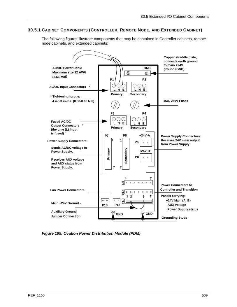
30.5 Extended I/O Cabinet Components
REF_1150 509
30.5.1 CABINET COMPONENTS (CONTROLLER, REMOTE NODE, AND EXTENDED CABINET)
The following figures illustrate components that may be contained in Controller cabinets, remote node cabinets, and extended cabinets:
L N E
L N EL N E
Primary
Primary
Secondary
Secondary
Prim
ary
Seco
ndar
y
+24V-A
+24V-B
AC/DC Power Cable
AC/DC Input Connectors
15A, 250V Fuses
Fused AC/DCOutput Connectors
Power Supply Connectors:Receives 24V main outputfrom Power Supply
Power Supply Connectors:
Sends AC/DC voltage to Power Supply.
Receives AUX voltageand AUX status fromPower Supply.
Fan Power ConnectorsPower Connectors to Controller and Transition
+24V Main (A, B) AUX voltage
Power Supply status
P1 P2
Maximum size 12 AWG(3.66 mm2)
Jumper Connection
Panels carrying:
P9P10
P11Main +24V Ground -
Auxiliary Ground
(the Line (L) input is fused)
P3 P4
P13
P7 P5
P6
P8
P12
L N E
GND
GNDGNDGrounding Studs
Copper straddle plate,connects earth groundto main +24V ground (GND).
1 7
1 2 5 7
1 1
7 7
* Tightening torque:4.4-5.3 in-lbs. (0.50-0.60 Nm)
*
*
Figure 195: Ovation Power Distribution Module (PDM)
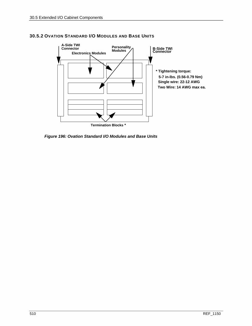
30.5 Extended I/O Cabinet Components
510 REF_1150
30.5.2 OVATION STANDARD I/O MODULES AND BASE UNITS
A-Side TWIConnector B-Side TWI
ConnectorElectronics Modules
Termination Blocks
PersonalityModules
* Tightening torque:5-7 in-lbs. (0.56-0.79 Nm)Single wire: 22-12 AWGTwo Wire: 14 AWG max ea.
*
Figure 196: Ovation Standard I/O Modules and Base Units

30.5 Extended I/O Cabinet Components
REF_1150 511
30.5.3 RELAY OUTPUT MODULES AND BASES
Electronics Module
Field Terminations
Relays
16 G2R Style Relays
Electronics Module
Field Terminations
Relays
12 KUEP Style Relays
A-Side TWIConnector B-Side TWI
Connector
Base Unit
A-Side TWIConnector
B-Side TWIConnector
Base Unit
*
* Tightening torque:*
* Tightening torque: 4.4-7.1 in-lbs. (0.50-0.80 Nm) Single Wire; 22-12 AWG (solid)22-14 AWG (stranded)
4.4-5.3 in-lbs. (0.50-0.60 Nm) Single wire: 22-12 AWG
Figure 197: Relay Output Modules and Bases
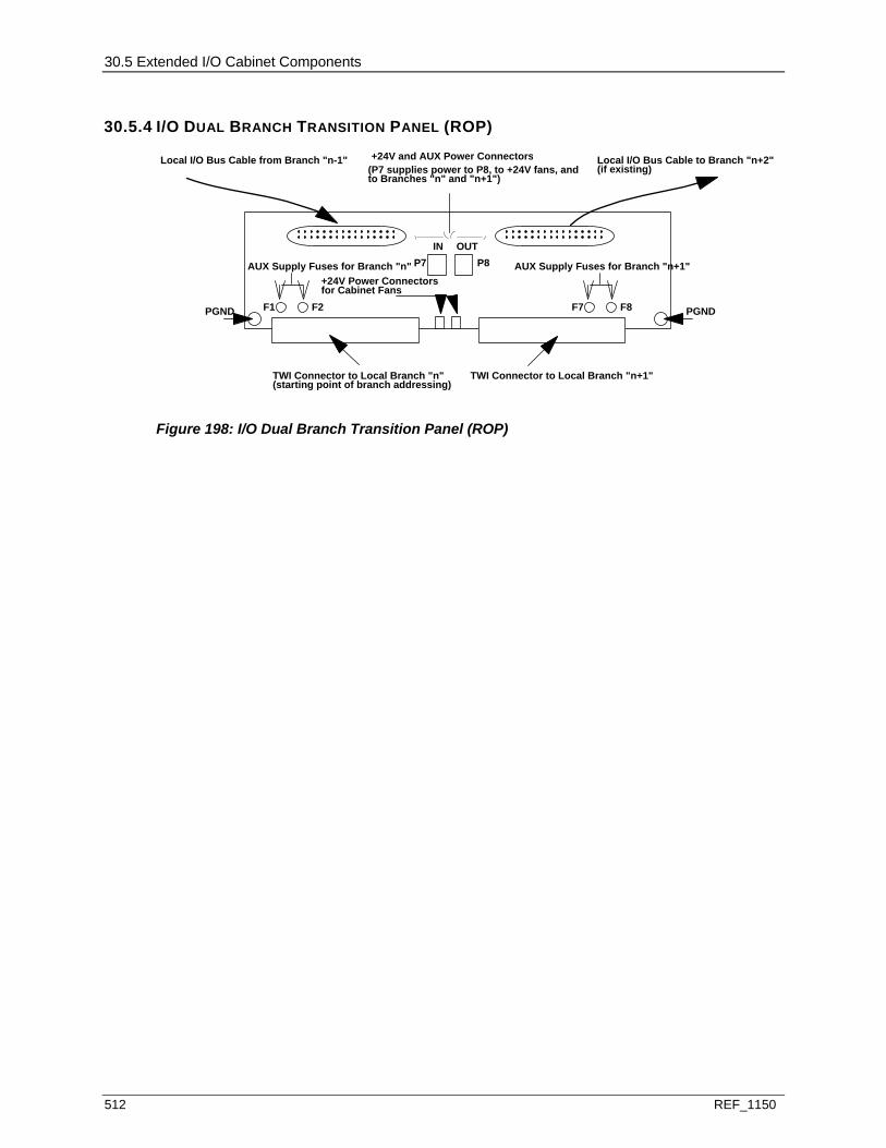
30.5 Extended I/O Cabinet Components
512 REF_1150
30.5.4 I/O DUAL BRANCH TRANSITION PANEL (ROP)
Local I/O Bus Cable from Branch "n-1" Local I/O Bus Cable to Branch "n+2"
+24V Power Connectorsfor Cabinet Fans
IN OUT
AUX Supply Fuses for Branch "n+1"P7 P8
(if existing)+24V and AUX Power Connectors
(P7 supplies power to P8, to +24V fans, and
F1 F2 F7 F8 PGNDPGND
AUX Supply Fuses for Branch "n"
TWI Connector to Local Branch "n" TWI Connector to Local Branch "n+1"
to Branches "n" and "n+1")
(starting point of branch addressing)
Figure 198: I/O Dual Branch Transition Panel (ROP)
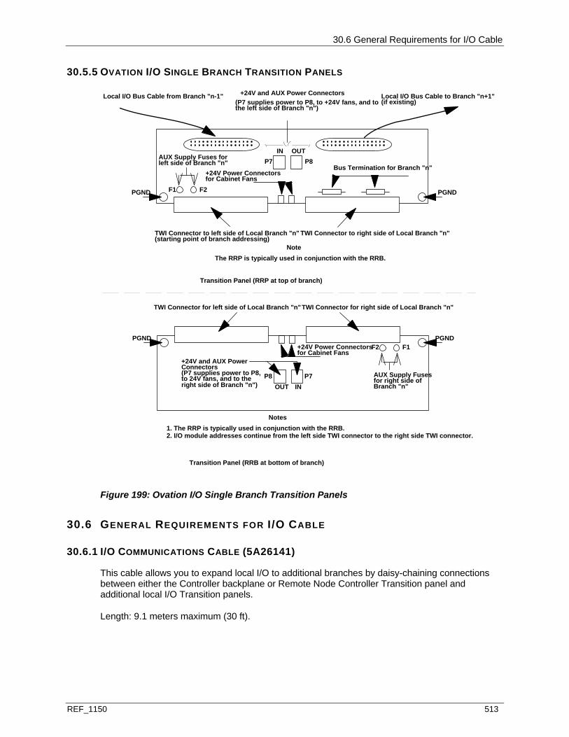
30.6 General Requirements for I/O Cable
REF_1150 513
30.5.5 OVATION I/O SINGLE BRANCH TRANSITION PANELS
Local I/O Bus Cable from Branch "n-1" Local I/O Bus Cable to Branch "n+1"
+24V Power Connectorsfor Cabinet Fans
IN OUTP7 P8
(if existing)+24V and AUX Power Connectors
(P7 supplies power to P8, to +24V fans, and to
F1 F2 PGNDPGND
AUX Supply Fuses for
TWI Connector to left side of Local Branch "n" TWI Connector to right side of Local Branch "n"
left side of Branch "n"
NoteThe RRP is typically used in conjunction with the RRB.
Bus Termination for Branch "n"
the left side of Branch "n")
(starting point of branch addressing)
OUT IN
TWI Connector for left side of Local Branch "n"TWI Connector for right side of Local Branch "n"
AUX Supply Fusesfor right side ofBranch "n"
F2 F1PGND PGND
P8 P7
+24V and AUX PowerConnectors(P7 supplies power to P8,
right side of Branch "n")
Notes1. The RRP is typically used in conjunction with the RRB.2. I/O module addresses continue from the left side TWI connector to the right side TWI connector.
+24V Power Connectorsfor Cabinet Fans
to 24V fans, and to the
Transition Panel (RRP at top of branch)
Transition Panel (RRB at bottom of branch)
Figure 199: Ovation I/O Single Branch Transition Panels
30.6 GENERAL REQUIREMENTS FOR I/O CABLE
30.6.1 I/O COMMUNICATIONS CABLE (5A26141)
This cable allows you to expand local I/O to additional branches by daisy-chaining connections between either the Controller backplane or Remote Node Controller Transition panel and additional local I/O Transition panels.
Length: 9.1 meters maximum (30 ft).
30.7 Configuring Remote I/O Cabinets
514 REF_1150
AUI Cable (5A26147)
The PCRR and Media Attachment Module are connected via an AUI cable. This cable meets the electrical specifications stated in the ANSI/IEEE 802.3 standard for Local Area Networks. The cable should be long enough to reach the length of the cabinet.
Length: Approximately 1.5 meters (5 ft).
Fiber-Optic Cable (3A98763 - Green) (3A98764 - Yellow)
The standard configuration of the Ovation Remote I/O Subsystem requires fiber-optic cables (with ST connectors) to connect the MAU to a remote node.
For 850 nm optics, distances of up to 2 km are supported between the remote node and the Controller or a repeater (up to two repeaters per communications link).
For 1300 nm optics, distances of up to 4 km are supported between the remote node and the Controller.
30.7 CONFIGURING REMOTE I/O CABINETS
30.7.1 PLACING THE MAU MODULE
The MAU module is located in an Ovation Controller cabinet or in a migrated WDPF DPU cabinet. The MAU plugs into a special base unit which can accommodate up to two modules per base. The base unit clamps onto the DIN rail, like standard I/O module bases.
MAU 1 and MAU 2 are two separate MAU modules which may be located anywhere in the Controller cabinet. One AUI cable connects (see page 515) MAU 1 to P1 on the PCRR, and a second AUI cable connects MAU 2 to P2 on the PCRR.
Note: If you migrate a WDPF Q-Line remote I/O system to Ovation, a QOR card will replace the QRC card in the WDPF Remote Node. Be sure to connect the MAU TX ports to the QOR RX ports, and connect the MAU RX ports to the QOR TX ports.
Refer to the applicable Remote Q-Line Installation Manual for your system for information on remote Q-Line and the QOR card (only 850 nm optics, with 2 km maximum length, are available for remote Q-Line applications).
The A-side and B-side of the MAU base unit terminates the local I/O bus, so the base must always be at the end of a branch when local I/O modules are located on the same branch.
The B-side of the MAU base also initiates base addressing for a branch of local I/O. If desired, multiple MAU base units may be connected together on a single branch. Since the MAU base unit terminates the local I/O bus, I/O Bus Termination cards are not required on the end of a branch that has an MAU.
Duplex fiber optic cables (see page 516) must be hooked between the MAU channels and their corresponding remote nodes with specific switch settings.
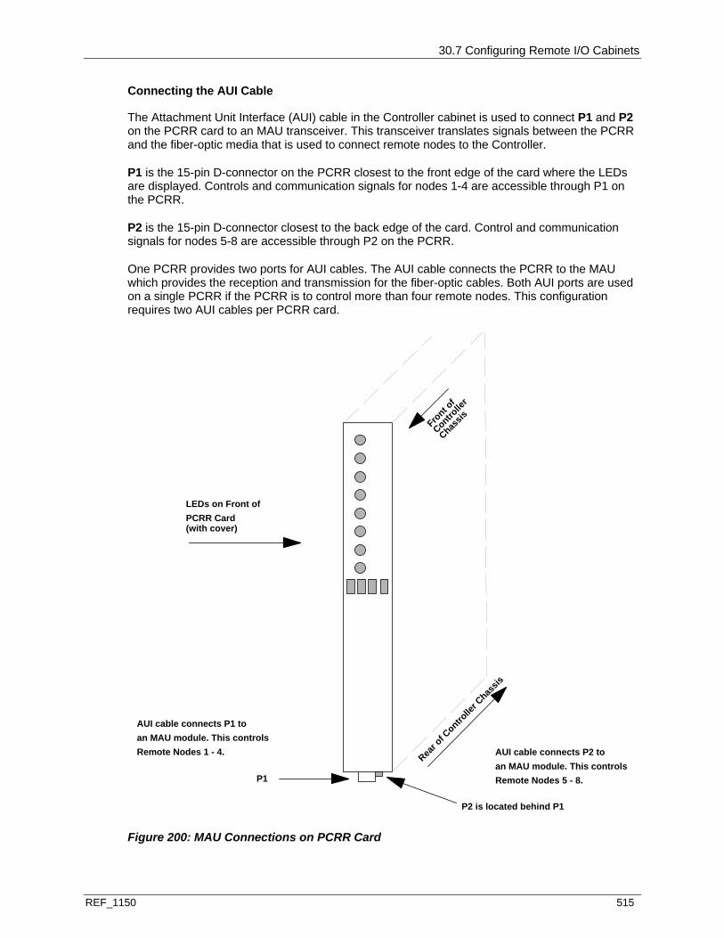
30.7 Configuring Remote I/O Cabinets
REF_1150 515
Connecting the AUI Cable
The Attachment Unit Interface (AUI) cable in the Controller cabinet is used to connect P1 and P2 on the PCRR card to an MAU transceiver. This transceiver translates signals between the PCRR and the fiber-optic media that is used to connect remote nodes to the Controller.
P1 is the 15-pin D-connector on the PCRR closest to the front edge of the card where the LEDs are displayed. Controls and communication signals for nodes 1-4 are accessible through P1 on the PCRR.
P2 is the 15-pin D-connector closest to the back edge of the card. Control and communication signals for nodes 5-8 are accessible through P2 on the PCRR.
One PCRR provides two ports for AUI cables. The AUI cable connects the PCRR to the MAU which provides the reception and transmission for the fiber-optic cables. Both AUI ports are used on a single PCRR if the PCRR is to control more than four remote nodes. This configuration requires two AUI cables per PCRR card.
P1
P2 is located behind P1
LEDs on Front of
Front o
f
PCRR Card
Rear o
f Contro
ller C
hassis
Controlle
r
Chassis
(with cover)
AUI cable connects P1 toan MAU module. This controlsRemote Nodes 1 - 4. AUI cable connects P2 to
an MAU module. This controlsRemote Nodes 5 - 8.
Figure 200: MAU Connections on PCRR Card
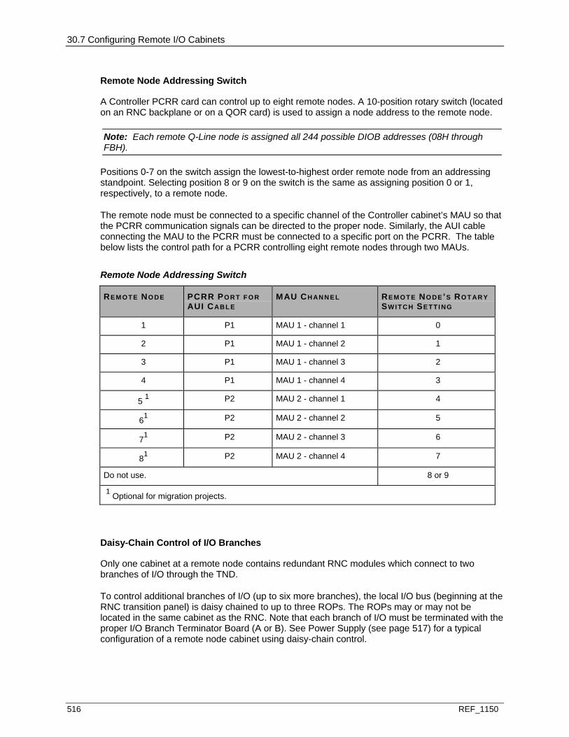
30.7 Configuring Remote I/O Cabinets
516 REF_1150
Remote Node Addressing Switch
A Controller PCRR card can control up to eight remote nodes. A 10-position rotary switch (located on an RNC backplane or on a QOR card) is used to assign a node address to the remote node.
Note: Each remote Q-Line node is assigned all 244 possible DIOB addresses (08H through FBH).
Positions 0-7 on the switch assign the lowest-to-highest order remote node from an addressing standpoint. Selecting position 8 or 9 on the switch is the same as assigning position 0 or 1, respectively, to a remote node.
The remote node must be connected to a specific channel of the Controller cabinet’s MAU so that the PCRR communication signals can be directed to the proper node. Similarly, the AUI cable connecting the MAU to the PCRR must be connected to a specific port on the PCRR. The table below lists the control path for a PCRR controlling eight remote nodes through two MAUs.
Remote Node Addressing Switch
REM O TE NO DE PCRR PO R T F O R AUI CABLE
MAU CH AN N E L REM O TE NO DE’S RO T AR Y SW I T C H SE TTI NG
1 P1 MAU 1 - channel 1 0
2 P1 MAU 1 - channel 2 1
3 P1 MAU 1 - channel 3 2
4 P1 MAU 1 - channel 4 3
5 1 P2 MAU 2 - channel 1 4
61 P2 MAU 2 - channel 2 5
71 P2 MAU 2 - channel 3 6
81 P2 MAU 2 - channel 4 7
Do not use. 8 or 9
1 Optional for migration projects.
Daisy-Chain Control of I/O Branches
Only one cabinet at a remote node contains redundant RNC modules which connect to two branches of I/O through the TND.
To control additional branches of I/O (up to six more branches), the local I/O bus (beginning at the RNC transition panel) is daisy chained to up to three ROPs. The ROPs may or may not be located in the same cabinet as the RNC. Note that each branch of I/O must be terminated with the proper I/O Branch Terminator Board (A or B). See Power Supply (see page 517) for a typical configuration of a remote node cabinet using daisy-chain control.

30.7 Configuring Remote I/O Cabinets
REF_1150 517
Power Supply
A +24V Power Supply is used to supply power to the Remote Node cabinet. The Power Supply is mounted on DIN Rails in the Remote Node cabinet. It is wired to the TND to provide power to the RNC and to the local I/O branches that are connected to the TND.
Up to 8 Remote Nodes per PCRRUp to 64 modules per NodeUp to 512 modules per PCRRUp to 2 PCRRs per ControllerUp to 1024 modules per Controller
Remote Node Limits
+24V
Prim
ary
Pow
er S
uppl
y
+24V
Bac
kup
Pow
er S
uppl
y
PowerDistributionModule
PCI P
roce
ssor
PCPS
Con
vert
er
NIC
PCR
L C
ard
PCR
R C
ard
PCI P
roce
ssor
PCPS
Con
vert
er
NIC
PCR
L C
ard
PCR
R C
ard
PrimaryController
BackupController
Br 1 Br 2Br 3 Br 4
PrimaryAUI Cable
BackupAUI Cable
+24V
Prim
ary
Pow
er S
uppl
y
+24V
Bac
kup
Pow
er S
uppl
y
Controller Cabinet(front and back)
Remote Node Cabinet #1(front and back)
Extended Cabinet(front and back)
MAU
ROP
RNC
TND
ROP
ROP
+24V
Prim
ary
Pow
er S
uppl
y
+24V
Prim
ary
Pow
er S
uppl
y
LocalComm.Cable
LocalComm.Cable
BackupRemoteCommunications
Cable
PrimaryRemoteComm.Cable
Figure 201: Example of Remote I/O Daisy-Chain Connections

30.8 Diagnostic LEDs
518 REF_1150
30.8 DIAGNOSTIC LEDS
Three Controller modules used in the Ovation Remote I/O subsystem are equipped with LEDs that provide diagnostic displays. The modules are the PCRR, MAU, and the RNC.
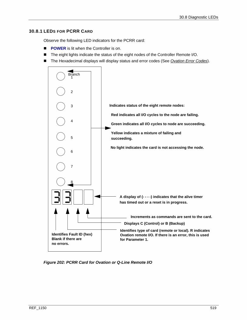
30.8 Diagnostic LEDs
REF_1150 519
30.8.1 LEDS FOR PCRR CARD
Observe the following LED indicators for the PCRR card:
POWER is lit when the Controller is on. The eight lights indicate the status of the eight nodes of the Controller Remote I/O. The Hexadecimal displays will display status and error codes (See Ovation Error Codes).
Indicates status of the eight remote nodes:
Identifies type of card (remote or local). R indicates
Red indicates all I/O cycles to the node are failing.
Green indicates all I/O cycles to node are succeeding.
Yellow indicates a mixture of failing and succeeding.
No light indicates the card is not accessing the node.
Identifies Fault ID (hex) Blank if there are
Displays C (Control) or B (Backup)
Increments as commands are sent to the card.
A display of (- - - -) indicates that the alive timerhas timed out or a reset is in progress.
no errors.
Ovation remote I/O. If there is an error, this is usedfor Parameter 1.
Branch 1
2
3
4
5
6
7
8
Figure 202: PCRR Card for Ovation or Q-Line Remote I/O

30.8 Diagnostic LEDs
520 REF_1150
MAU Module
The MAU Electronics Module front panel has LEDs to display the status of the MAU on-board power supply and the fiber-optic links between the MAU and each remote node.
The four LINK OK LEDs correspond with the four remote nodes connected to the MAU.
Note: G01 MAU contains only two remote node connections and does have Link 3 and Link 4 LEDs.
P 1 2 3 4
P (Power) is green when the VCC is above the minimum acceptable threshold.
1 through 4 is green for a specific MAU channel when thechannel's receiver detects a healthy link to its correspondingremote node.
L
I
N
K
O
K
L
I
N
K
O
K
L
I
N
K
O
K
L
I
N
K
O
K
Figure 203: MAU LED Indicators
A healthy link between an MAU channel and a remote node is established when the transmitter of a powered-up remote node Controller is connected through a fiber-optic link to the receiver of its corresponding channel on the MAU. The transmitted signal received by the MAU must be strong enough to overcome low-light conditions to be seen as healthy by the MAU.
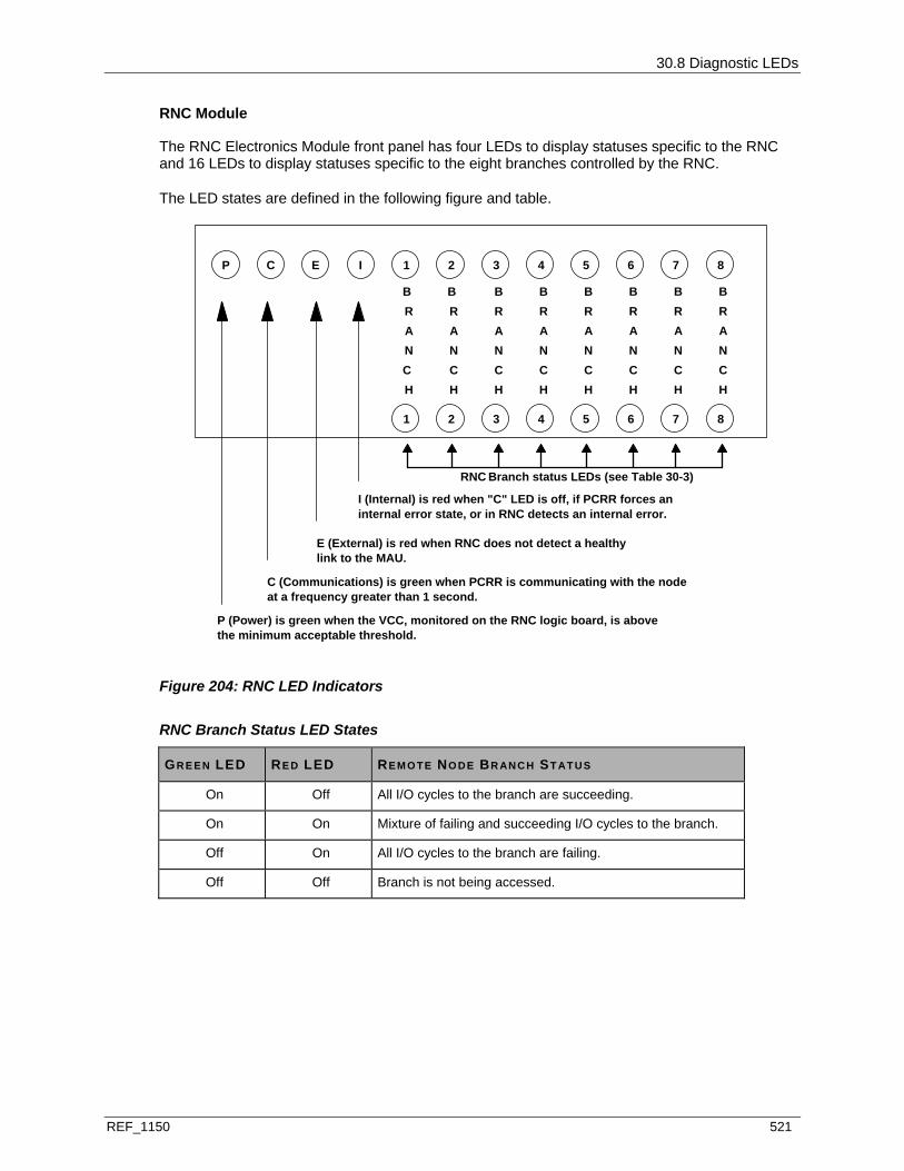
30.8 Diagnostic LEDs
REF_1150 521
RNC Module
The RNC Electronics Module front panel has four LEDs to display statuses specific to the RNC and 16 LEDs to display statuses specific to the eight branches controlled by the RNC.
The LED states are defined in the following figure and table.
P 1 2 3 4
P (Power) is green when the VCC, monitored on the RNC logic board, is abovethe minimum acceptable threshold.
BRAN
H
C E I 5 6 7 8
C
1 2 3 4 5 6 7 8
BRAN
HC
BRAN
HC
BRAN
HC
BRAN
HC
BRAN
HC
BRAN
HC
BRAN
HC
C (Communications) is green when PCRR is communicating with the nodeat a frequency greater than 1 second.
E (External) is red when RNC does not detect a healthy link to the MAU.
I (Internal) is red when "C" LED is off, if PCRR forces an internal error state, or in RNC detects an internal error.
Branch status LEDs (see Table 30-3)RNC
Figure 204: RNC LED Indicators
RNC Branch Status LED States
GR E E N LED RE D LED REM O TE NO DE BR ANCH ST ATUS
On Off All I/O cycles to the branch are succeeding.
On On Mixture of failing and succeeding I/O cycles to the branch.
Off On All I/O cycles to the branch are failing.
Off Off Branch is not being accessed.


REF_1150 523
A.1 Analog Types
Analog Data Types
DAT A TY P E DE S C RI P T I O N
0 Not applicable
1 Not applicable
2 Not applicable
3 16 bit signed analog input card, card status =15, confide = 14, sign = 13,
signed over range = 12, value = 11 to 0
4 16 bit unsigned analog input card, card status =15, unsigned over range = 13,
value = 12 to 0
5 16 bit unsigned analog input card, value = 15 to 0
6 16 bit signed analog input card, card status = 0, sign = 15,
unsigned over range = 1, value = 13 to 3
7 16 bit unsigned analog input card, card status =15 and 0, unsigned over range = 1, value = 13 to 3
8 16 bit unsigned analog input card, card status = 15, value = 11 to 0
9 16 bit unsigned analog output card, value = 15 to 0
10 16 bit signed analog output card, sign = 15, value = 14 to 4
11 16 bit unsigned analog output card, value = 15 to 4
12 16 bit unsigned analog output card, clamped at 16, value = 15 to 4
13 16 bit unsigned analog output card, scaled by.6 and biases + 800,
value = 15 to 4
22 16 bit unsigned analog input card, card status = 15, value = 14 to 0
A P P E N D I X A
Q-LINE CARD TYPES

A.1 Analog Types
524 REF_1150
Analog Card Types
CARD GR O UP WDPF I I CARD TYP E
RANG E DAT A TYP E
QAA G01 NA -16 to +16mA (Position)
+4 to +20 mA (Velocity)
0
G02 NA +4 to +20 mA (Velocity)
-10 to +10 VDC (Voltage) Optional
0
QAH G01 17 -10.24 to +10.235 V 6
G02 18 -5.12 to + 5.117 V 6
G03 19 0 to +10.237 V 7
G04 20 0 to 5.119 V 7
QAI G01 1 -20 to +20 mV 3
G02 2 -50 to +50 mV 3
G03 3 -100 to +100 mV 3
G04 4 -500 to +500 mV 3
G05 5 -1 to +1 V 3
G06 6 -10 to + 10 V 3
G07 7 or 9 0 to 20 mA 3
G07A NA 4 to 20 mA 3
G08 8 -50 to +50 mV 3
QAM G01 31 0 to 10 VDC (Output) 0
G02 31 0 to 10 mA, 0 to +5 VDC (Output) 0
QAO G01 21 0 to + 20.475 mA 12
G01A 29 4.00 to + 20.475 mA 13
G02 22 -0 to +10.2375 V 11
G03 23 -10.24 to +10.235 V 10
G04 24 0 to +5.1187 V 11
G05 25 -5.12 1 to +5.1175 V 10
G06 26 -10.24 to + 10.235 V 10
G07 27 0 to + 20.475 mA 12
G07A NA +4 to +20 mA 12
G08 28 -10.24 to + 10.235 V 10
QAV G01 1 or 54 -20 to +20 mV 3
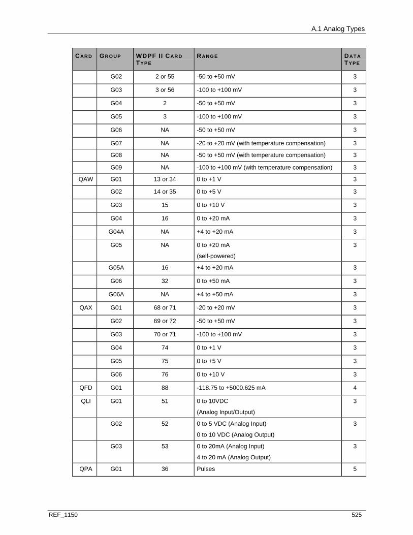
A.1 Analog Types
REF_1150 525
CARD GR O UP WDPF I I CARD TYP E
RANG E DAT A TYP E
G02 2 or 55 -50 to +50 mV 3
G03 3 or 56 -100 to +100 mV 3
G04 2 -50 to +50 mV 3
G05 3 -100 to +100 mV 3
G06 NA -50 to +50 mV 3
G07 NA -20 to +20 mV (with temperature compensation) 3
G08 NA -50 to +50 mV (with temperature compensation) 3
G09 NA -100 to +100 mV (with temperature compensation) 3
QAW G01 13 or 34 0 to +1 V 3
G02 14 or 35 0 to +5 V 3
G03 15 0 to +10 V 3
G04 16 0 to +20 mA 3
G04A NA +4 to +20 mA 3
G05 NA 0 to +20 mA
(self-powered)
3
G05A 16 +4 to +20 mA 3
G06 32 0 to +50 mA 3
G06A NA +4 to +50 mA 3
QAX G01 68 or 71 -20 to +20 mV 3
G02 69 or 72 -50 to +50 mV 3
G03 70 or 71 -100 to +100 mV 3
G04 74 0 to +1 V 3
G05 75 0 to +5 V 3
G06 76 0 to +10 V 3
QFD G01 88 -118.75 to +5000.625 mA 4
QLI G01 51 0 to 10VDC
(Analog Input/Output)
3
G02 52 0 to 5 VDC (Analog Input)
0 to 10 VDC (Analog Output)
3
G03 53 0 to 20mA (Analog Input)
4 to 20 mA (Analog Output)
3
QPA G01 36 Pulses 5

A.2 Digital Types
526 REF_1150
CARD GR O UP WDPF I I CARD TYP E
RANG E DAT A TYP E
G02 36 Pulses 5
G03 36 Pulses 5
G04 36 Pulses 5
QRT G01 NA 0 to + 10 mV 3
G02 NA 0 to + 33 1/3 mV 3
QSD G01 NA Input: 20 V peak-to-peak
1 KHz sine wave (LVDT)
Output: +/- 24 mA
0
QSR G01 NA 0 to 100 8
G02 NA NA 8
G03 NA NA 8
G04 NA NA 8
QSS G01 66 1.5, 1.8, 3.0, 3.6, 6.0, or 7.2 kHz 22
A.2 Digital Types
Digital Data Types
DAT A TY P E DE S C RI P T I O N DAT A TY P E DE S C RI P T I O N
1 Standard digital input card 8 Not applicable
2 Standard digital output card 9 Not applicable
3 Not applicable 10 Not applicable
4 Not applicable 11 Not applicable
5 Not applicable 12 Not applicable
6 Not applicable 13 Not applicable
7 Not applicable NA NA
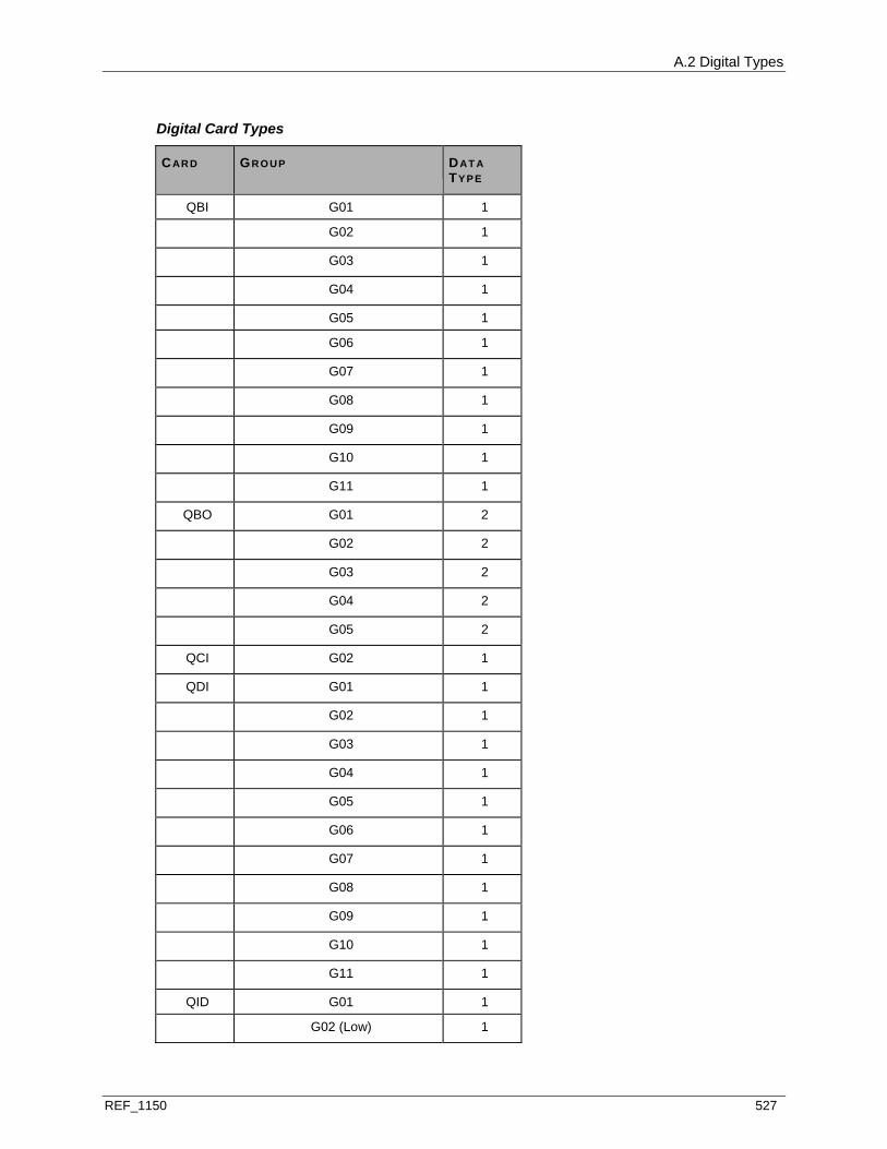
A.2 Digital Types
REF_1150 527
Digital Card Types
CARD GR O UP DAT A TYP E
QBI G01 1
G02 1
G03 1
G04 1
G05 1
G06 1
G07 1
G08 1
G09 1
G10 1
G11 1
QBO G01 2
G02 2
G03 2
G04 2
G05 2
QCI G02 1
QDI G01 1
G02 1
G03 1
G04 1
G05 1
G06 1
G07 1
G08 1
G09 1
G10 1
G11 1
QID G01 1
G02 (Low) 1
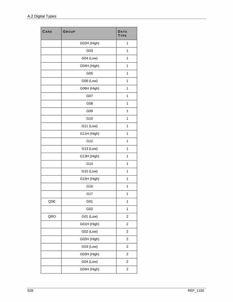
A.2 Digital Types
528 REF_1150
CARD GR O UP DAT A TYP E
G02H (High) 1
G03 1
G04 (Low) 1
G04H (High) 1
G05 1
G06 (Low) 1
G06H (High) 1
G07 1
G08 1
G09 1
G10 1
G11 (Low) 1
G11H (High) 1
G12 1
G13 (Low) 1
G13H (High) 1
G14 1
G15 (Low) 1
G15H (High) 1
G16 1
G17 1
QSE G01 1
G02 1
QRO G01 (Low) 2
G01H (High) 2
G02 (Low) 2
G02H (High) 2
G03 (Low) 2
G03H (High) 2
G04 (Low) 2
G04H (High) 2

A.3 Packed Point Types
REF_1150 529
A.3 Packed Point Types
Packed Data Types
DAT A TY P E DE S C RI P T I O N
1 Standard 16 bit digital input card
2 Standard 16 bit digital output card
3 Not applicable
4 Not applicable
5 Not applicable
6 Not applicable
7 Not applicable
8 Not applicable
9 Not applicable
10 Not applicable
11 Not applicable
12 Not applicable
13 Not applicable
Digital Card Types
CARD GR O UP DAT A TY P E
QBI G01 1
G02 1
G03 1
G04 1
G05 1
G06 1
G07 1
G08 1
G09 1
G10 1
G11 1
QBO G01 2
G02 2
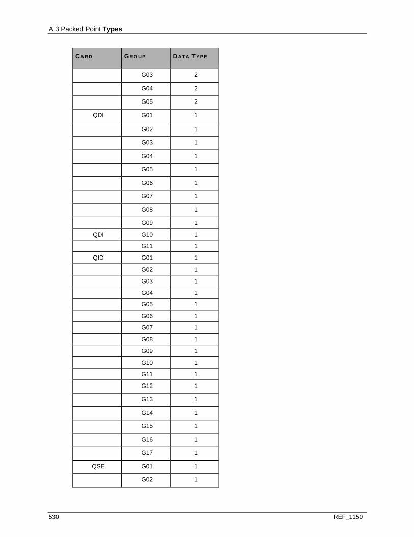
A.3 Packed Point Types
530 REF_1150
CARD GR O UP DAT A TY P E
G03 2
G04 2
G05 2
QDI G01 1
G02 1
G03 1
G04 1
G05 1
G06 1
G07 1
G08 1
G09 1
QDI G10 1
G11 1
QID G01 1
G02 1
G03 1
G04 1
G05 1
G06 1
G07 1
G08 1
G09 1
G10 1
G11 1
G12 1
G13 1
G14 1
G15 1
G16 1
G17 1
QSE G01 1
G02 1
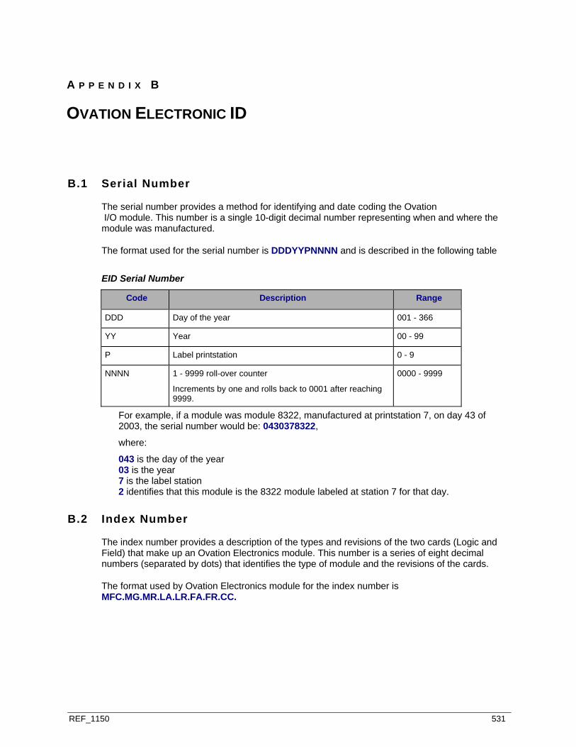
REF_1150 531
B.1 Serial Number
The serial number provides a method for identifying and date coding the Ovation I/O module. This number is a single 10-digit decimal number representing when and where the module was manufactured.
The format used for the serial number is DDDYYPNNNN and is described in the following table
EID Serial Number
Code Description Range
DDD Day of the year 001 - 366
YY Year 00 - 99
P Label printstation 0 - 9
NNNN 1 - 9999 roll-over counter
Increments by one and rolls back to 0001 after reaching 9999.
0000 - 9999
For example, if a module was module 8322, manufactured at printstation 7, on day 43 of 2003, the serial number would be: 0430378322,
where:
043 is the day of the year 03 is the year 7 is the label station 2 identifies that this module is the 8322 module labeled at station 7 for that day.
B.2 Index Number
The index number provides a description of the types and revisions of the two cards (Logic and Field) that make up an Ovation Electronics module. This number is a series of eight decimal numbers (separated by dots) that identifies the type of module and the revisions of the cards.
The format used by Ovation Electronics module for the index number is MFC.MG.MR.LA.LR.FA.FR.CC.
A P P E N D I X B
OVATION ELECTRONIC ID
B.2 Index Number
532 REF_1150
EID Index Number (Ovation I/O Modules)
Code Description Range Number of Bits
MFC Module Function Code 1 001 - 254 8
MG Module Assembly Group 00 - 63 6
MR Module Assembly Revision 00 - 63 6
LA Logic Card Artwork 00 - 31 5
LR Logic Card Assembly Revision 00 - 63 6
FA Field Card Artwork 00 - 31 5
FR Field Card Assembly Revision 00 - 63 6
CC Compatibility Code 00 - 63 6
1 Refer to the following table for each Ovation I/O module.
The format used by the I/O Controller cards (PCRL, PCRR, PCQL and QOR) for the index number is MFC.MG.CR.CA and is described in below:
EID Index Number (Ovation I/O Controller Modules)
Code Description Range Number of Bits
MFC Module Function Code 1 001 - 254 8
CG Controller Group 01 - 63 6
CR Controller Assembly Revision 00 - 63 6
CA Controller Artwork 00 - 31 5
1 Refer to the following table for function codes for each Ovation I/O Controller module.
Module Function Codes
Module Assembly
Module Type Category Function Code
1C31113 Analog Input (AI) I/O Module 001
1C31129 Analog Output (AO) I/O Module 002
1C31107 Digital Input (DI) I/O Module 003
1C31122 Digital Output (DO) I/O Module 004
1C31142 Contact Input (CI) I/O Module 005
1C31157 Sequence of Events (SE) I/O Module 006
1C31147 Pulse Accumulator (PA) I/O Module 007
1C31166 Link Controller (LC) I/O Module 008

B.2 Index Number
REF_1150 533
Module Assembly
Module Type Category Function Code
1C31199 Servo Driver (SR) I/O Module 009
1C31194 Valve Positioner (VP) I/O Module 010
1C31189 Speed Detector (SD) I/O Module 011
1C31203 Remote Node Controller (ND) I/O Module 012
1C31179 Media Attachment Unit (AU) 1 I/O Module 013
1C31161 RTD Input (RT) I/O Module 014
1C31174 Loop Interface Controller (LI) I/O Module 015
1C31219 Relay Output Electronics (ROE) I/O Module 016
1C31232 Compact Digital Input (DI) I/O Module 017
1C31234 Compact Contact Input (CI) I/O Module 018
1C31233 Compact Sequence of Events (SE) I/O Module 019
1C31224 14-bit Analog Input (AI14) I/O Module 020
5X00058 HART Analog Input (HAI) I/O Module 021
5X00062 HART Analog Output (HAO) I/O Module 022
5X00070 High-Speed Analog Input (HSAI) I/O Module 023
5X00106 Isolated HART Analog Input (IAH) I/O Module 024
5X00119 8 Channel RTD Input (RTD) I/O Module 025
3A99257 Q-line Remote Node Controller (QOR) I/O Controller 250
3A99229 PCI to GBUS Interface (PGI) PGI 251
3A99190 Remote Ovation I/O Interface (PCRR) I/O Controller 252
3A99158 Local Ovation I/O Interface (PCRL) I/O Controller 253
3A99141 Local Q-line I/O Interface (PCQL) I/O Controller 254
1 No on-board EID. Bar code label only.
B.3 I/O Module EID Programming Format
534 REF_1150
B.3 I/O Module EID Programming Format
The EID is represented in the Electronics card of an I/O module as five 16-bit integers (words). These words are programmed into the card after it has been manufactured and tested.
B.3.1 SERIAL NUMBER
The entire 10-digit serial number is written as one number into two 16-bit words. The serial number is contained in the MH field of the Module (RM) Record Type and the Node (RN) Record Type (See the Record Types Manual.)
B.3.2 INDEX NUMBER
The 17-digit index number is packed into three 16-bit words. The index number is contained in the M6, M7, and M8 fields of the Module (RM) Record Type and the Node (RN) Record Type (See Ovation Record Types Manual.)
Index high word: Index # 3: M8 field (offset d)
bit 15
bit 14
bit 13
bit 12
bit 11
bit 10
bit 9 bit 8 bit 7 bit 6 bit 5 bit 4 bit 3 bit 2 bit 1 bit 0
MFC MFC MFC MFC MFC MFC MFC MFC MG MG MG MG MG MG MR MR
Index middle word: Index # 2: M7 field (offset c)
bit 15
bit 14
bit 13
bit 12
bit 11
bit 10
bit 9 bit 8 bit 7 bit 6 bit 5 bit 4 bit 3 bit 2 bit 1 bit 0
MR MR MR MR LA LA LA LA LA LR LR LR LR LR LR FA
Index low word: Index # 1: M6 field (offset b)
bit 15
bit 14
bit 13
bit 12
bit 11
bit 10
bit 9 bit 8 bit 7 bit 6 bit 5 bit 4 bit 3 bit 2 bit 1 bit 0
FA FA FA FA FR FR FR FR FR FR CC CC CC CC CC CC

B.4 Bar Code Label
REF_1150 535
B.4 Bar Code Label
The following figures contain examples of bar code labels. These labels are typically placed on the bottom of a manufactured Ovation Electronics I/O module or I/O Controller board after it has been successfully tested.
S/N: 2699700629 INDEX: 003.02.01.04.03.02.01.00
Module Serial Number
(MFC) Module Function Code
(MG) Module Assembly Group
(MR) Module Assembly Revision
(LA) Logic Card Artwork
(LR) Logic Card Revision
(FA) Field Card Artwork
(FR) Field Card Revision
(CC) Compatibility Code ** The Compatibility Code applies to select modules only. If no compatibility code is required, then
the field is set to "00."
Area may containa manufacturing "M" number.
Area mayindicate country ofassembly.
Figure 205: Bar Code Example for I/O Module
B.4 Bar Code Label
536 REF_1150
S/N: 2699700629 INDEX: 003.02.01.04
Module Serial Number
(MFC) Function Code
(CG) Assembly Group
(CR) Assembly Revision
(CA) Card Artwork
* The Compatibility Code applies to select modules only. If no compatibility code is required, thenthe field is set to "00."
Area may containa manufacturing "M" number.
Area mayindicate country ofassembly.
Figure 206: Bar Code Example for I/O Controller Board
REF_1150 537
The CE Mark Certified Ovation system uses special EMC cabinets, supplementary internal filtering, and exacting requirements on field wiring and grounding to ensure compliance with specific European Electromagnetic Emissions/Immunity and Low voltage safety.
The CE Mark Certified Ovation Controller cabinet assembly, extended I/O cabinet assembly, and Remote I/O cabinet assembly are certified for operation in the Industrial Environment as documented in the EMC Technical Construction File for Ovation (5A16444) and the Low Voltage Safety Technical File for Ovation (5A26443). The specific requirements for the CE Mark Certified Systems can be located in the following:
Drawing 5A26418 - This drawing contains a baseline listing of all components applicable for the CE Mark Certified System.
Drawing 5A26370 - This drawing contains a baseline listing of workstation and peripheral components applicable for the CE Mark Certified System.
The appropriate Planning and Installing Your Ovation System for your system provides information about CE Mark requirements for an Ovation system.
A P P E N D I X C
CE MARK SPECIFICATIONS

REF_1150 539
D.1 What is an External Supply
Some Ovation I/O modules require an auxiliary power supply. Auxiliary power may be obtained either from the internal auxiliary power supply (backplane), or from an external power supply.
The auxiliary power is bussed along an entire branch of I/O modules. All I/O modules within a branch MUST use the same auxiliary power voltage for proper operation. External auxiliary power can be applied to each branch individually.
If an Ovation I/O module is to be connected to an external power supply, perform the following procedure BEFORE connecting the power supply to the Ovation module and powering it up.
Note: We do NOT recommend using external auxiliary power with the Relay Output module. Instead, use the Ovation internal auxiliary supply for relay coil power.
D.2 To Prepare for Connecting an External Power Supply
CAUTION! Using an external power supply may introduce dangerous voltages to an I/O cabinet. Do NOT apply external power to a cabinet until the appropriate internal auxiliary power supply fuses have been removed and the required fuse covers have been installed.
1. Identify the specific I/O branch to which the Ovation I/O module is assigned and the back panel (CBO) or transition panel (ROP or TND) associated with the I/O branch (see Figure and Figure for panel locations).
2. If the I/O branch is associated with a transition panel, refer to Figure and perform the following:
a) If the transition panel has a cover, remove it in order to expose the fuses.
b) Remove the pair of round plug-in fuses located nearest the I/O branch that you identified in Step 1.
c) Replace the transition panel cover (where applicable) after the fuses are removed. A fuse cover kit is not required for transition panels that have a cover. However, if the transition panel does not have a cover, then fuse cover caps (5A26371H20) are required.
Note: Fuse cover caps are required only if the external power supply output voltage is greater than 60 VDC, 42 VAC peak or 30 VAC rms.
3. If the I/O branch is associated with a backplane (CBO), refer to Figure and perform the following:
a) Identify the artwork level of the backplane.
b) Determine what fuse cover kit is needed for the backplane:
A P P E N D I X D
USING AN EXTERNAL POWER SUPPLY
D.2 To Prepare for Connecting an External Power Supply
540 REF_1150
1C31213G01 for artwork level 3CBO and earlier
1C31213G02 for artwork level 5CBO and later
a) Remove the pair of round plug-in fuses located nearest the I/O branch that you identified in Step 1.
b) Install the appropriate fuse cover kit over the fuse sockets from where the fuses were removed.
Note: The fuse cover kit is required only if the external power supply output voltage is greater than 60 VDC, 42 VAC peak or 30 VAC rms.
4. After the fuse covers are securely installed, connect the external voltage power supply positive (+) and negative (-) outputs to the Ovation I/O module base unit terminal block PS+ (A17 or B17) and PS- (A18) terminals. Once the external power supply is connected to the base unit terminal block and is powered up, the entire I/O branch has access to the external power supply voltage.
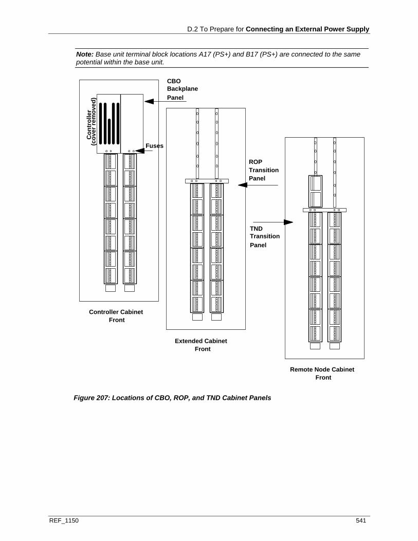
D.2 To Prepare for Connecting an External Power Supply
REF_1150 541
Note: Base unit terminal block locations A17 (PS+) and B17 (PS+) are connected to the same potential within the base unit.
Front
Con
trol
ler
ROP
PanelTransition
(cov
er re
mov
ed)
Fuses
Controller Cabinet
CBO
PanelBackplane
TND
PanelTransition
FrontRemote Node Cabinet
FrontExtended Cabinet
Figure 207: Locations of CBO, ROP, and TND Cabinet Panels
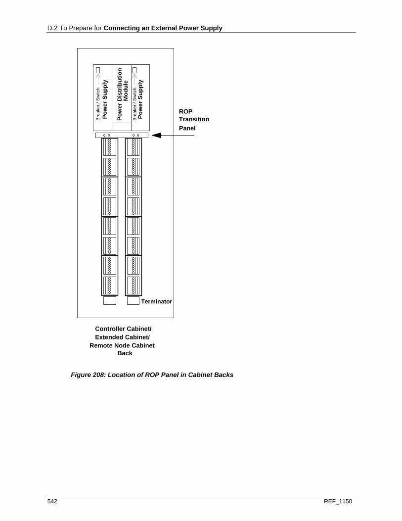
D.2 To Prepare for Connecting an External Power Supply
542 REF_1150
Back
Pow
er S
uppl
y
Pow
er S
uppl
y
Pow
er D
istr
ibut
ion
Mod
ule
Terminator
ROP
Panel
TransitionBre
aker
/ S
witc
h
Bre
aker
/ S
witc
h
Controller Cabinet/Extended Cabinet/
Remote Node Cabinet
Figure 208: Location of ROP Panel in Cabinet Backs
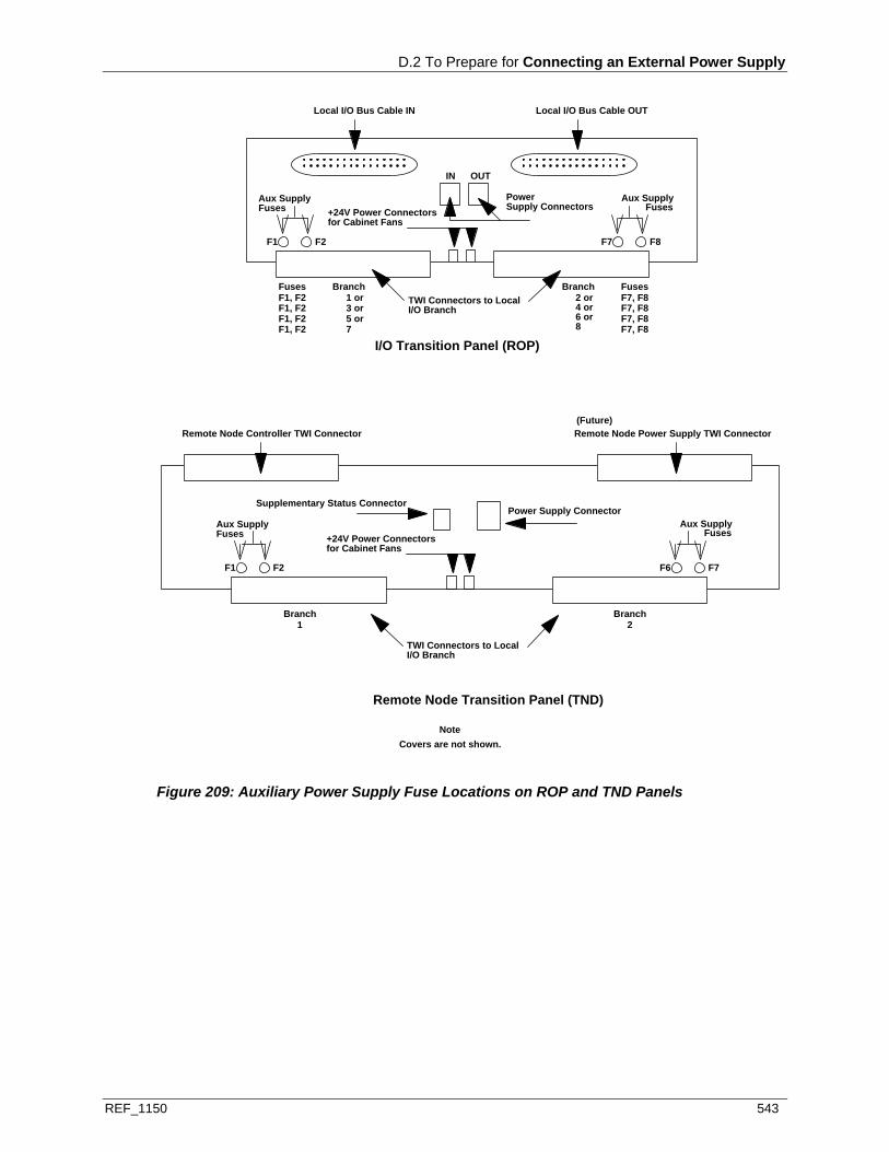
D.2 To Prepare for Connecting an External Power Supply
REF_1150 543
I/O Transition Panel (ROP)
Local I/O Bus Cable IN Local I/O Bus Cable OUT
TWI Connectors to LocalI/O Branch
+24V Power Connectorsfor Cabinet Fans
PowerSupply Connectors
IN OUT
+24V Power Connectorsfor Cabinet Fans
Remote Node Controller TWI Connector Remote Node Power Supply TWI Connector
TWI Connectors to LocalI/O Branch
Power Supply ConnectorSupplementary Status Connector
Remote Node Transition Panel (TND)
(Future)
Branch1 or3 or5 or
Branch2 or4 or6 or
Branch1
Branch2
7 8
Aux SupplyFuses
F7 F8
Covers are not shown.Note
Aux SupplyFuses
F1 F2
Aux SupplyFuses
F6 F7
Aux SupplyFuses
F1 F2
FusesF1, F2F1, F2F1, F2F1, F2
FusesF7, F8F7, F8F7, F8F7, F8
Figure 209: Auxiliary Power Supply Fuse Locations on ROP and TND Panels

D.2 To Prepare for Connecting an External Power Supply
544 REF_1150
Notes
1. Remove fuses from backplane if voltage power is provided externally.
2. Remove fuse cover kit from bag and attach to backplane as shown.
Controller Backplane
Branch 1
Branch 2
3. Artwork level is printed on backplane. Refer to this to determine the appropriate fuse cover kit to use.
5CBO
ARTWORK LEVELSEE NOTE 3
Figure 210: Fuse Locations on Backplane

REF_1150 545
A A PORT
Port on a dual-attached Ovation station where the primary ring enters and the secondary ring exits.
ADMIN TOOL
The Administrative Tool is an Emerson utility that configures and downloads software to the drops through the use of GUIs. (Do not confuse this tool with the Sun utility also named Admin Tool.)
ALARM
A message or other signal intended to draw attention to a non-normal plant condition; for displays at user interfaces, an alarm reflects a point status.
ALGORITHM
1) A set of rules, procedures, and mathematical formulas that define a desired control strategy. 2) Software provided with a Controller to automatically apply a specified algorithm during the system scan. 3) Ovation record type (LC) used to store tuning or data configuration for an algorithm in the system.
ANALOG
1) Conditions or values that continuously vary across some range, represented by more than one bit. 2) A point that is an analog record type. Analog points are typically associated with I/O hardware that converts a field signal (for example, voltage) to a low-level signal used by the processor. Can be Long or Deluxe (Contrast with digital.)
APERIODIC POINTS
Points whose values are scanned only as needed or as requested. See also periodic points.
API
Application Programming Interface, a set of routines or functions a program calls to tell the operating system to perform a task.
APPLICATION PROGRAM
1) Emerson-supplied programs that perform frequently required functions. 2) A series of loops, ladders, and/or algorithms run in a processor to control plant functions. Also known as an Application. 3) User-defined or commercially available software that performs a specific task.
APPLY
GUI button that accepts changes and window remains open.
GLOSSARY OF TERMS
Glossary of Terms
546 REF_1150
ASCII
American Standard Code for Information Interchange, a standard for representing computer characters. The set consists of 128 characters numbered from 0 to 127 and includes all the letters, numbers and punctuation marks.
ASYNCHRONOUS
Data communication that is not time critical. Typically provided on demand only and provided at different times (Contrast with synchronous).
AUI CABLE
Attachment Unit Interface Cable that interfaces the PCRR card to the MAU module in Ovation and WDPF migrated remote I/O applications. It contains four sets of individually shielded twisted pairs.
B B PORT
Port on a dual-attached Ovation station where the secondary ring enters and the primary ring exits.
BANDWIDTH
This is a description of how much information can be sent through a connection, usually measured in bits-per-second.
BASE ALARM SYSTEM
Standard package used for viewing and acknowledging alarms.
BASE UNIT
Hardware that consists of a printed circuit board, various connectors, and plastic housing and provides a mechanism for the user to land field wiring, and connects the field signals to the I/O module. The unit enables the I/O module to receive power, and also provides a low-impedance earth ground connection. Each Base Unit can house two sets of I/O modules, along with the associated field wiring.
BAUD RATE
Number of bits-per-second a modem can send or receive.
BG
See Packed Group Alarm.
BIT
A single digit number in base-2, either a 1 or a zero. This is the smallest unit of computerized data.
BITMAP FILE
A file type that is used to define which icons will be shown when using iconic alarming.
Glossary of Terms
REF_1150 547
BOOTSTRAP
A software routine used to start computer operation (sometimes abbreviated ‘boot’). The bootstrap routine will typically occur automatically after a reset or power cycle, but may require manual keying.
BRANCH
Set of Base Units configured consecutively on a DIN rail with a local bus being connected to the Ovation I/O controller.
BRIDGE
Device that connects two or more network components and transmits data with source and destination addresses on different network components.
BROADCAST
Process of sending information across the Ovation network. Broadcasts may be periodic (every second or every 0.1 of a second) or non-periodic (broadcast on demand only).
BYTE
A set of bits that represent a single character. Typically, 8 or 10 bits in a byte.
C CANCEL
GUI button that cancels changes and dismisses window.
CDDI
Copper Distributed Data Interface (See FDDI).
CDE
Common Desktop Environment. A windowing system that runs on a Sun-compatible workstation under SunOs™ or Solaris™
CHARACTERISTICS
A set of 8 alphanumeric characters associated with a point, used to represent user-defined aspects of the controlled process. Characteristics are used in alarm processing and point review/search functions.
CLIENT
A computer, or software program that is used to contact and obtain data from a server software program on a networked computer.
COIL
A ladder diagram element that represents either a real-world output field device (for example, a motor starter, solenoid, etc.) or an internal calculated point. (See discrete output.)

Glossary of Terms
548 REF_1150
COLLISION
Garbling of data when two or more nodes on the same network segment transmit data simultaneously.
COLLISION DETECTION
Switches are used to buffer simultaneous data messages and transmit them one at a time.
COMPACT I/O MODULES
Ovation I/O modules that do not contain a Personality module, only an Electronics module.
CONCENTRATOR
FDDI node used to connect multiple Ovation stations to dual rings. Must have an “A” port, a “B” port, and at least one “M” port.
CONDUCTING
The state of a ladder diagram circuit when there is a continuous current path condition caused by closed contacts.
CONFIGURATION
Entering initial data into a processor, including definition of associated hardware. The configuration process typically includes downloading the drop database and other required software, and may involve editing configuration files(s).
CONFIGURATION FILE
Typically, an ASCII file containing statements that specify the configuration of a drop or function. These files may use standard operating system formats or may use an Emerson source language.
CONTACT
A ladder diagram element that represents either a real-world input device (for example, a push-button, switch, etc.) or an internal calculated point. (See discrete input.)
CONTROL BUILDER
AutoCAD based Power tool package used to build control drawings and generate source code from the drawings.
CONTROL SHEET
AutoCAD drawing that contains a graphical representation of a control scheme.
CONTROL TASK
Specific Controller area where all control sheets in that area are scanned at the same frequency.
CONTROLLER
A drop used to control a process. The Controller passes process control information over the network to other drops or devices that need it.

Glossary of Terms
REF_1150 549
CPU
Central Processing Unit, a microprocessor chip that powers a computer. May also refer to the case that holds the chip.
CRT
Cathode-Ray Tube, a tube of a monitor that produces images on the screen. Often used as a generic term for a computer monitor.
CURSOR
A character on a display screen indicating the current active location.
D DAC/DAS
Dual Attachment Concentrator/Dual Attachment Station. Provides dual attachment to the FDDI or Fast Ethernet network.
DATA HIGHWAY
The communication link used to transfer time-critical information between drops or stations; also called a Local Area Network (LAN) or network.
DATA STRUCTURES
Four portions of an Ovation point record type.See also Dynamic Data, Static Data, Flash Data, and MMI Data.
DATABASE
A structured set of data, especially the point database in each Ovation drop (which defines originated and received points) and the Ovation master database (which defines the attributes of all points in the system).
DCS
Distributed Control System (such as Ovation).
DEADBAND
Range of values through which an input signal may vary without initiating an action that causes an observable change in the output signal.
DEFAULT POINTS
Points created by the Control Builder that have a defined naming convention.
DEFAULT VALUE
Used by a program when no specific value has been entered by the user. In the context of an iterative window or program, default may refer to a value specified in the function’s configuration file; in the context of configuring a function, default refers to the value used when there is no valid parameter entry.

Glossary of Terms
550 REF_1150
DELUXE RECORD TYPE
Optional Ovation record type. Has same functions as Long record type, plus plant mode limits and scan time displays.
DESTINATION
1) The location in memory (such as a holding register) into which data is placed after the completion of certain programmable functions. (Contrast with source.) 2) A method of determining which alarms will be displayed at a specific user interface drop, based on the first point characteristic (typically representing the plant area).
DEVELOPER STUDIO
Common interface that houses all of the integrated engineering tools necessary for a Microsoft Windows based Ovation system.
DEVICE
1) Peripheral equipment connected to the Ovation system. 2) Algorithm specifically designed to simplify operation of open/close or stop/start devices, using feedback signals to monitor command completion.
DHC
Data Highway Controller. Printed-circuit board(s) in each drop that manage Data Highway communication.
DIAGNOSTICS
Functions that examine hardware or software to isolate malfunctions and errors. In the Ovation system, each drop incorporates automatic self-test diagnostics. If faulty operation is detected, a message or alarm is usually initiated.
DIAGRAM
A graphic depiction ofa plant process (or other data), displayed on a CRT at a user interface.
DIALOG BOX
A user interface window that prompts the user to enter information needed by a process.
DIGITAL
1) Signals or conditions that are either on or off, represented by one bit. 2) A point that is a digital record type. Digital points are typically associated with discrete I/O hardware. Can be Long or Deluxe. (Contrast with analog.)
DIN
German standards organization (Deutsche Industrie Norm).
DIP
Integrated circuit enclosed in a plastic or ceramic housing and connected to pins. (Dual Inline Package)
Glossary of Terms
REF_1150 551
DISCRETE I/O
Individual hard-wired circuits connecting real-world field devices with the processor. Each discrete input provides the processor with a single digital signal based on a single state in the field device. Each discrete output sends a single digital signal to the field based on a single bit of data in the processor.
DISTRIBUTED DATABASE
Contains a subset of the information stored on the Master Database and is stored locally on a drop to allow that drop to operate if the Master Database is unavailable. A Distributed Database is present on each drop in the system and is continually updated as point information changes.
DISTRIBUTED I/O
Hardware used to communicate between the processor and I/O modules located outside the processor chassis (also called Remote I/O).
DOMAIN
Logical collection of computers and users on a network that share a common security database.
DOWNLOAD
The process of transferring data to the memory or disk of a drop.
DROP
A collective term for a Controller, Workstation, or Database Server that is a member of an Ovation network and is defined as a drop by an Ovation configuration tool (Developer Studio or Init Tool).
DROP LOADER
Power Tool used to load control and originating point information into drops in an Ovation system. Links the Master Database with all the drops in the system.
DROP POINT (DU)
Record type used to store status information for a drop. Every drop must be configured with at least one point of type DU.
DYNAMIC DATA
Portion of an Ovation point record that is broadcast periodically in Dynamic Data Blocks (DDBs )by the originating drop and stored in volatile memory. DDB size is configured through the Ovation configuration tools (Admin Tool or Developer Studio).
E EDB HISTORIAN
A drop on an Ovation control system that will collect, process, archive, and retrieve information that originates locally or throughout a geographically diverse set of process control sites.
Glossary of Terms
552 REF_1150
ELECTRONICS MODULE
Part of Ovation I/O that contains the electronics for processing I/O signals. Fits into the Base Unit and is typically configured by a Personality Module.
EMS
Expanded Memory Specification, a bank-switched memory management scheme that allows applications to access vast quantities of memory.
ENGINEERING STATION
An Ovation drop used for configuration and entry of system programs.
ETHERNET
A standard network protocol. Used to transfer non-time-critical information between drops.
F FAST ETHERNET
Standard for transmitting data at 100 megabits per second. Similar to FDDI, but uses switches instead of concentrators, and dual-channel Ethernet NIC cards instead of dual-attachment FDDI NIC cards (Contrast to FDDI).
FDDI
Fiber Distributed Data Interface, a standard for transmitting data. Typically consists of a dual fiber-optic counter-rotating ring capable of carrying synchronous and asynchronous messages. Ring provides automatic “wrap-back” reconfiguration if a segment of the highway fails (Contrast to Fast Ethernet).
FIREWALL
Security system intended to protect an organization's computer network from external threats. All communication between the internal computer network and the outside world is routed through a server that determines if a message is safe to pass to the internal network.
FLASH DATA
Portion of an Ovation point record that is stored in the originating drop’s flash (or disk) memory and copied to receiving drop’s periodically.
FORCE VALUE
To set the value of a coil or contact to a desired state (on/off; 0, 1), regardless of other values in the ladder diagram.
FOUNDATION FIELDBUS
Digital, two-way, multi-drop communication link among intelligent measurement and control devices.

Glossary of Terms
REF_1150 553
FTP
File Transfer Protocol, a set of rules that allows one computer to download a file from another computer via a network connection.
FULLY QUALIFIED POINT NAME
Point name that specifically identifies a point by combining three parameters. Format is pointname.unit@network where point name contains a maximum of 16 characters, unit contains a maximum of 6 characters, network contains a maximum of 8 characters. Do not use when inserting a new point in Developer Studio, only insert point name parameter.
G GATEWAY
Hardware or software that translates between two dissimilar protocols.
GP
See Packed Group.
GRAPHICS BUILDER
Power Tool used to create and edit System Process Diagrams that display on the Operator Station.
GUI
Graphical User Interface, an industry-standard term used to describe a user interface based on a windowing system such as Microsoft Windows™.
H HISTORIAN
Dedicated drop in the Ovation system that collects and stores process point data and other information.
HMI
Human Machine Interface. Refers to drops that provide user interface functions.
HOST
Any computer on a network that is available for services to other computers.
HYPERTEXT
Any text that contains “links” to other documents-words or phrases in the document that can be chosen by the reader and which cause another document to be retrieved and displayed.
I I/O
Input/Output, a general term for reading and writing data on a computer. Digitizes information from plant processes and passes it to the Controller for use in control strategies.

Glossary of Terms
554 REF_1150
I/O BUILDER
Power Tool used to define the I/O modules used in an Ovation system.
I/O CONTROLLER
Interface between the Network and the I/O. The Controller is located in the Ovation I/O cabinet.
I/O MODULE
Typically made up of an Electronics module and a Personality module. Performs the interface between the I/O Controller and the field devices.
I/O NODES
Ovation record types
ICON
A small graphic on a windowing system display that represents an active process or available function. Typically, an icon can be expanded into a window.
ICONIC ALARMING
Provides a mechanism to group alarms based on their priority and their plant area. Each group of alarms is represented by a preconfigured bitmap on the display.
INIT TOOL
Initialization Tool. Ovation utility that defines the system drops and the software packages on the drops through the use of GUIs.
IOIC CARD
Generic name for the Ovation I/O Interface card. Also known as PCI card. Options are PCQL, PCRL, and PCRR cards.
IP ADDRESS
A unique number consisting of 4 parts separated by dots, (for example, 129.228.36.38). Every computer that is on the Internet has a unique IP address.
ISA
Industry Standard Architecture, the 8- and 16-bit bus design used in most PCs.
K KB
Kilobyte, A thousand bytes, (actually 1024 bytes).

Glossary of Terms
REF_1150 555
L LADDER
1) A diagram representing relay-type control logic (see coil, contact). 2) The user's control application program written in a variation of relay logic representation.
LAN
Local Area Network, A computer network limited to the immediate area, usually the same building.
LICENSE
A necessary permission to use certain Emerson Process Control software products.
LOG SERVER
Utility used to define and modify custom reports for an Ovation system. Also known as Report Builder or Report Server.
LOGIN
1) The account name used to gain access to a computer system. 2) The act of entering into a computer system.
LONG RECORD TYPE
Default record type for Ovation points. Has full alarming and I/O capabilities.
LOOP
1) A diagram representing a modulating or continuous process control. 2) The modulating control system for a particular physical process.
LOOP INTERFACE MODULE (LIM)
M/A Station interface connected to QLI card.
M M PORT
Port on a Concentrator that attaches to a drop or station.
M/A STATION
Manual/Automatic Station. May be a diagram (sometimes called a “soft” M/A Station) that simulates the functions of a traditional panel-mounted control device. The M/A Station allows the operator to select manual or automatic control of the output, and to manipulate the set point or output value (depending on the selected control mode).

Glossary of Terms
556 REF_1150
MAN PAGES
UNIX on-line documentation for operating system functions. Type “man” and the desired topic.
MASTER DATABASE
Contains the entire process database. It is used for creating, modifying, and verifying control strategies and process points. At runtime, it supports queries of the process database, captures changes made to control and point attributes, and propagates those changes to the distributed database.
MAU
Media Attachment Unit. Interfaces the PCRR card (via the AUI cable) to an Ovation RNC card or a WDPF QOR card.
MB
Megabyte, A million bytes, a thousand Kilobytes.
MENU
A screen display representing a set of functions available to the user.
MIGRATION
Process where Q-Line I/O is interfaced to an Ovation Controller.
MMI
Man-Machine Interface. Refers to drops that provide user interface functions (such as the Operator Station).
MMI DATA
Portion of the Ovation point record that is saved in the Distributed Database in every Ovation workstation.
MODEM
MOdulator and DEModulator, A device that connects to a computer and to a phone line that allows the computer to talk to other computers through the phone system.
MODULE POINT (RM)
Ovation record type used to configure and monitor status of Ovation I/O modules.
MONITOR
1) To observe the operation of a process without influencing it. 2) A computer terminal or CRT.
MULTIPLE NETWORKS
Function that enables separate Ovation Networks to communicate with each other, share data, and perform control actions.
Glossary of Terms
REF_1150 557
N NETWORK
Two or more computers connected together so they can share resources.
NETWORK FOLDER
A subfolder of the System folder in the Ovation Developer Studio. Only one Network folder can exist in the system. The Network folder is the parent folder to all files, objects, and folders that pertain to the Network.
NIC
Network Interface Card. Located in Ovation Controller cabinets, Stations, or HMIs.
NODE
1) Any single computer connected to a network. 2) Active element on an FDDI or Fast Ethernet network that has an address. Can be a station or a concentrator. Up to 1000 nodes are permitted per network.
NODE POINT (RN)
Node point is used to configure and monitor PCRL, PCRR, PCRQ cards, and remote I/O nodes.
O OPENWINDOWS
A windowing system that runs on a Sun-compatible workstation under SunOs™ or Solaris™.
OPERATOR STATION
A drop in an Ovation system used to control and monitor plant operation.
ORIGINATED POINTS
Points that were created in the current drop.
OVATION I/O
Line of Emerson I/O modules.
OVATION KEYBOARD
Also known as the Membrane Keyboard, a specialized keyboard that is connected to an Ovation Operator Station serial port and allows the user to execute a set of standard functions from the keyboard.
OVATION NETWORK
Redundant, deterministic, high-speed network used for process control. Based on Fast Ethernet standards, it supplies input and output data to all the stations and Controllers connected to it.
Glossary of Terms
558 REF_1150
OVATION SYSTEM
An open architecture Emerson Process Control System that is based on ANSI and ISO network standards. Uses snap-in modules for I/O.
P PACKED DIGITAL POINT (PD)
A point that is a packed digital record type. Holds either 32 separate digital values or two 16-bit register (analog) values.
PACKED POINT
A point that is a packed point record type. Packs up to 16 digital (logical) bits in one point record. Each bit may be separately configured for I/O scanning. Can be Long or Deluxe.
PASSWORD
A code used to gain access to a locked system.
PC
1) Common acronym for personal computer 2) Common acronym for programmable controller.
PCI
Peripheral Component Interconnect. Generic name for the Ovation I/O Interface card. Also known as IOIC card. Options are PCQL, PCRL, and PCRR cards.
PCL
Printer Control Language. Printer language that drives most laser and inkjet printers.
PCQL CARD
Ovation IOIC card used to interface with Q-Line modules.
PCRL CARD
Ovation IOIC card used to interface with local Ovation modules.
PCRR CARD
Ovation IOIC card used to interface with remote Ovation modules and remote Q-Line I/O modules in migrated systems.
PDS
Process Diagram System. Contains graphics that are displayed on the Ovation Operator Station.

Glossary of Terms
REF_1150 559
PERIODIC POINTS
Points whose values are scanned periodically at a defined frequency such as every 1 second or every 0.1 of a second. See also aperiodic points.
PERSONALITY MODULE
Part of Ovation I/O that configures the Electronics Module. Fits into the Base Unit beside the Electronic Module that it configures.
PID
Proportional, Integral, Derivative. A type of closed-loop, modulating control function. It acts according to an algorithm that detects deviations between a predetermined set point and an actual process variable input condition or value.
PLANT MODE
Defines the current state of a plant (value range 1 - 6). Alarm limits can be defined that are based on plant mode. Can be defined in Deluxe points.
POINT
A record in the Ovation master database containing a value (such as an input or output) and related data.
POINT BUILDER
Power Tool used to create, modify, and delete Ovation points.
POKE FIELD
A location in a diagram where the cursor can be placed, allowing the operator to select an option.
PORT
1) A connection where information goes into or out of a computer. 2) Translating a piece of software to bring it from one type of computer system to another.
POWER TOOLS
Set of unified and flexible engineering tools used to configure and maintain the Ovation system. All objects (such as points) created by the tools are stored in a master database.
PROCESS DIAGRAMS
Graphical images that represent actual plant process control equipment. Part of the Process Diagram System (PDS) used at the Operator Station.
PROCESSING TIME
The time, in milliseconds, required to make one complete pass through a Controller application program.
Glossary of Terms
560 REF_1150
Q Q-LINE
Legacy line of Emerson I/O modules.
QUALITY
Indicates point condition to Operator Station and to the algorithms.
R RADIO BUTTON
Button appears as a small circle that, when selected, has a smaller, filled circle inside it. Selecting one button in a set deselects the previously selected button so one and only one of the options in a set can be selected at any given time.
RAM
Random Access Memory, the generic term for memory that can be written to and read from.
RECEIVED POINTS
Points that were not created in the current drop.
RECORD
The set of data associated with a point, including the point name, System ID, value, status, and various other fields, depending on the point record type.
REFRESH
Refreshes the display to the current contents of the object's database values.
REGISTER
A data storage area in memory. In the Controller, there are four types: input registers (R), output registers (O), holding registers (H), and dynamic holding registers (G). At times, however, input groups (I) and output groups (C) are used as if they were an input or output register.
RELATIONAL DATABASE
Central database (Oracle) for Ovation systems. Uses tables to store and locate information.
REMOTE I/O
A hardware configuration where the I/O is located remotely from the Controller.
REMOTE NODE
A grouping of I/O modules that communicates with the Controller via media that can carry control signals over a long distance (for example, fiber-optic).

Glossary of Terms
REF_1150 561
REVIEW
Data retrieved from the Ovation network. Reviews can be retrieved based on point status requests and/or point characteristics.
RING
Set of nodes where data is passed sequentially between nodes, examined or copied, and returned to the originating node.
RISC
Reduced Instruction-Set Computing, a microprocessor architecture that contains a smaller instruction set in order to increase processor speed.
RNC
Remote Node Controller (RNC) is an alternate name for the Ovation module containing the Remote Node Electronics module and Remote Node Personality module. The RNC interfaces the I/O modules in the Remote Node to an MAU module at the Controller via a fiber-optic communication link
ROM
Read-Only Memory, the generic term for memory that can read from but not be written to.
ROP
I/O hardware transition panel.
ROUTER
A hardware or software set-up that handles the connection between two or more networks.
S S PORT
Port on a station that connects to an M port.
SAC/SAS
Single Attachment Concentrator/Single Attachment Station. Provides a single attachment to the FDDI or Fast Ethernet network.
SCAN
The processor module's sequential and ongoing examination of each contact circuit, control relay, special function, and process control loop in the application program. During the scan, the processor accesses data stored in memory and the current states of the field I/O. The result is the energizing or de-energizing of the coils and the determination of analog output information.
SCSI
Small Computer System Interface, a peripheral-connect interface used to connect hard drives, CDROM drives, and other storage devices to a computer.
Glossary of Terms
562 REF_1150
SECURITY BUILDER
Ovation Power Tool that defines, configures, and manages security for an Ovation system.
SELECT
1) For control applications, choosing the algorithm to be controlled, typically through an M/A Station. 2) Highlighting an item on the screen, such as an item on a menu or in a scrolling list, as a means of choosing an option.
SERVER
A computer, or software program that provides a specific kind of service to a client software running on other computers.
SETPOINT
The desired value of a process variable. In modulating control, other variables are continuously modified to maintain the value of the controlled variable at the setpoint.
SGML
Standard Generalized Markup Language, a text-based language for describing the content and structure of digital documents.
SID
See System ID.
SIMULATOR
Software package that runs on an actual Ovation Controller. Can use either simulated or actual I/O hardware to test control logic.
SMARTPROCESS
Emerson’s plant optimization software used to improve plant processes.
SNMP
Simple Network Management Protocol. An Ovation program designed to monitor and report the activity in various devices on the network.
SOE
Sequence of Events. SOE messages are transferred from Controllers to certain drops on the network.
SOFTWARESERVER
A drop on a network that provides storage and control of system software files.
Glossary of Terms
REF_1150 563
SOURCE
1) A location, in memory, that is the origin of the data to be moved or converted. This may be a register or, at times, an input group used as a register. 2) An ASCII input file containing commands or statements in a programming language.
STATIC DATA
Portion of the Ovation point record that is stored in volatile memory by the originating drop and broadcast to receiving drops on an as-needed basis. The receiving drop stores it in its volatile memory.
STATION
Addressable node on FDDI or Fast Ethernet network; can transmit, repeat, and receive data.
SVGA
Super Video Graphics Array, an extension of the VGA video standard. SVGA enables video adapters to support up to 16.7 million colors, known as true colors in a 1024-by-768 pixel display.
SWITCH
Fast Ethernet device used to connect multiple Ovation Stations to the network.
SYNCHRONOUS
High speed data communication that is time critical. Must be guaranteed service for nodes transmitting synchronous data. Typically provided periodically.
SYSTEM FOLDER
The parent folder to all files, objects, and folders that pertain to that System in the Ovation Developer Studio.
SYSTEM ID
System Identification number (SID). The Data Highway reference number for each point which may be transmitted.
SYSTEM TREE
The system file structure in the Ovation Developer Studio.
T TCP/IP
Transmission Control Protocol / Internet Protocol, a set of communication protocols that allows dissimilar computers to share information over a network.
TERMINAL
1) Solaris window where commands are entered. 2) A device that allows the user to send commands to a remote computer.
Glossary of Terms
564 REF_1150
TIFF
Tagged Image File Format, a file format for bit-mapped graphics that stores the information in discrete blocks called tags.
TND
Remote Node transition panel.
TOKEN
A field in the Drop Status Record (DSR) that identifies the drop that broadcast a message.
TOOLBAR
A row of icons that activate commands or functions when clicked.
TREND
A display that plots point values over a selected time interval. Trend displays may be generated based on data from the MMI trend history, from a Historian, or from an eDB.
TUNING
Manually changing the value of point record fields or algorithm record fields.
U UNIT FOLDER
The subfolder of a Network in the Ovation Developer Studio. The Unit folder is a parent folder to all files, objects, and folders that pertain to that particular unit.
UNIX
An operating system used in Ovation drops. Ovation uses the Solaris version of UNIX.
V VGA
Video Graphics Array, a standard graphics adapter that enables video adapters to support 16 colors in a 640-by-480 pixel display.
VIRTUAL CONTROLLER
Software representation of an actual Ovation Controller, but no Controller hardware is required. Virtual Controllers have the same functionality as real Controllers, but do not actually connect to plant I/O.
W WINDOW
A screen display using only part of the CRT, often movable and resizable.
Glossary of Terms
REF_1150 565
WINDOWS
Microsoft 32-bit multitasking Operating System (such as NT or XP).
WYSIWYG
What You See Is What You Get, when the appearance of the screen output matches exactly (or very closely) the printed output.
Z ZOOM
A way of enlarging or reducing a specific area in a graphic.

REF_1150 567
1 13-Bit Analog Input Field Connection Wiring
Diagrams (CE Mark Certified) • 47 13-Bit Analog Input Field Connection Wiring
Diagrams (Non-CE Mark Certified) • 46 13-Bit Analog Input Terminal Block Wiring
Information • 44 14-Bit Analog Input Field Connection Wiring
Diagrams (CE Mark Certified) • 60 14-Bit Analog Input Field Connection Wiring
Diagrams (Non-CE Mark Certified) • 59 14-Bit Analog Input Terminal Block Wiring
Information • 57
4 4 to 20 mA Signal Considerations • 14
8 8-Channel RTD Ranges • 332
A A Port • 555 AD/DA Conversion and Timing • 380 Address Location Information • 48, 60, 82,
98, 111, 124, 135, 149, 175, 190, 204, 218, 233, 264, 285, 303, 315, 327, 344, 354, 368, 375, 405, 426, 477
Admin Tool • 555 Alarm • 555 Algorithm • 555 Analog • 555 Analog High Speed Input Module (14 bits) •
67 Analog Input Module (13 bits) • 37 Analog Input Module (14 bits) • 55 Analog Input Modules • 23 Analog Output Field Connection Wiring
Diagrams (CE Mark Certified) • 98 Analog Output Field Connection Wiring
Diagrams (Non-CE Mark Certified) • 97 Analog Output Module • 95 Analog Output Modules • 23 Analog Output Terminal Block Wiring
Information • 96 Analog Signal Noise Rejection • 9 Analog Signal Shielding Techniques • 12 Analog Types • 531 Aperiodic Points • 555 API • 555
Application program • 555 Apply • 555 ASCII • 556 Assemblies • 420 Assigning Thermocouple Coefficients • 41,
71 Asynchronous • 556 AUI Cable • 556 AUI Cable (5A26147) • 522
B B Port • 556 Backup to Primary • 439 Bandwidth • 556 Bar Code Label • 545 Base Alarm System • 556 Base Unit • 556 Baud Rate • 556 BG • 556 Bit • 556 Bitmap file • 556 Blown Fuse Detection Circuit • 166, 297 Bootstrap • 557 Branch • 557 Bridge • 557 Broadcast • 557 Byte • 557
C Cabinet Components (Controller and
Extended Cabinet) • 496 Cabinet Components (Controller, Remote
Node, and Extended Cabinet) • 517 Calibrate Mode • 384, 443 Calibrating Redundant LVTs • 389 Calibration • 458 Calibration Goals • 462 Calibration Ideal • 388, 460 Calibration Procedure • 387 Calibration Required • 386, 459 Cancel • 557 CDDI • 557 CDE • 557 CE Mark Certified System • 148 CE Mark Certified Systems • 81, 110, 123,
134, 258 CE Mark Certified Systems Using
Personality Module 1C31164G02 • 314 CE Mark Considerations • 14 CE Mark Specifications • 547 CE Mark Systems • 79
INDEX
Index
568 REF_1150
Channel Error Bit • 235 Channel Scale Configuration Registers • 328 Characteristics • 557 Client • 557 Coil • 557 Coil Setup • 440 Collision • 558 Collision Detection • 558 Compact Contact Input Cable Impedances
in Field Wiring • 121 Compact Contact Input Front End Field
Connection Wiring Diagrams • 120 Compact Contact Input Module • 115 Compact Contact Input Terminal Block
Wiring Information • 117 Compact Digital Input Module • 139 Compact Digital Input Terminal Block Wiring
Information • 141 Compact I/O Modules • 558 Compact Sequence of Events Module • 357 Compact SOE Contact Input Configuration
and Status Register • 375 Compact SOE Contact Input Field
Connection Wiring Diagram (CE Mark) • 374
Compact SOE Contact Input Field Connection Wiring Diagram (Non-CE Mark) • 375
Compact SOE Contact Input Field Interface • 370
Compact SOE Contact Input Terminal Block Wiring Information • 373
Compact SOE Digital Input Configuration and Status Register • 368
Compact SOE Digital Input Field Connection Wiring Diagram (CE Mark) • 367
Compact SOE Digital Input Field Connection Wiring Diagram (Non-CE Mark) • 366
Compact SOE Digital Input Module Emod (1C31233G01 through G03) • 363
Compact SOE Digital Input Terminal Block Wiring Information • 365
Concentrator • 558 Conducting • 558 Configuration • 558 Configuration and Status Register • 48, 60,
90, 98, 111, 124, 135, 149, 175, 190, 218, 234, 264, 285, 303, 315, 327, 405, 426, 477
Configuration Commands • 448 Configuration File • 558 Configuring Remote I/O Cabinets • 522 Connecting the AUI Cable • 523 Contact • 558 Contact Closure Signal Considerations • 14
Contact Input Cable Impedances in Field Wiring • 108
Contact Input Field Interface • 347 Contact Input Front End Field Connection
Wiring Diagrams • 107 Contact Input Module • 103 Contact Input Terminal Block Wiring
Information • 105 Contingency Check Error • 479 Control Builder • 558 Control Sheet • 558 Control Task • 558 Controller • 558 Controller Backplane (CBO) • 493, 508 Controller Cabinet Components (Local I/O) •
490 Controller Cabinet Components (Remote
I/O) • 504 Controller Cabinet Components and Cabling
(local and remote I/O) • 507 Controller Cabinet Components and Cabling
(local I/O) • 492 Controller Interface • 392, 444 Controller Watchdog Timer • 410 Copyright Notice • 2 CPU • 559 CRT • 559 Cursor • 559
D DA Readback Error • 479 DAC/DAS • 559 Daisy-Chain Control of I/O Branches • 524 Data Highway • 559 Data Structures • 559 Database • 559 DCS • 559 Deadband • 559 Default Points • 559 Default Value • 559 Deluxe record type • 560 Demodulator Gain • 482 Description • 37, 55, 67, 95, 104, 116, 127,
139, 153, 179, 197, 211, 227, 239, 241, 273, 293, 309, 321, 336, 358, 379, 414, 421, 489, 503
Description and Guidelines for Redundant VP Module • 433
Description for Single VP Module • 432 Description of Terms • 2 Descriptions • 432 Destination • 560 Developer Studio • 560 Device • 560 DHC • 560

Index
REF_1150 569
Diagnostic LEDs • 52, 63, 91, 100, 112, 125, 136, 150, 176, 193, 208, 223, 237, 266, 289, 304, 317, 330, 355, 377, 410, 427, 484, 526
Diagnostic LEDs, Compact Sequence of Events Digital Input • 369
Diagnostic LEDs, Sequence of Events Digital Input • 346
Diagnostics • 409, 479, 560 Diagnostics of LVDT Problems for
Redundant VP • 481 Diagram • 560 Dialog Box • 560 Digital • 560 Digital Input Field Interface • 338, 361 Digital Input Module • 127 Digital Input Modules • 24 Digital Input Terminal Block Wiring
Information • 131 Digital Output Address Locations • 175 Digital Output Field Connection Wiring
Diagrams • 168 Digital Output Module • 153 Digital Output Modules • 24 Digital Output Terminal Block Wiring
Information • 166 Digital Signal Considerations • 14 Digital Types • 534 DIN • 560 DIP • 560 Discrete I/O • 561 Distributed Database • 561 Distributed I/O • 561 Domain • 561 Download • 561 Drop • 561 Drop Loader • 561 Drop Point (DU) • 561 During Automatic Calibration • 483 Dynamic Data • 561
E eDB Historian • 561 EEPROM Checksum • 409 Electronic Module (Emod) • 293 Electronic Modules (Emods) • 242, 435 Electronics Module • 562 Electronics Module (Emod) • 67, 104, 116,
153, 179, 198, 211, 227, 239, 322, 421 Electronics Module Fuses • 31 Electronics Modules (Emods) • 37, 55, 95,
127, 140, 273, 309, 337, 359, 381 EMS • 562 Energy Level • 6 Engineering Station • 562 EPROM Checksum Error • 409, 479
Ethernet • 562 Example of Typical MAU Cable Connections
to Remote Nodes • 510 Expansion Configuration and Status
Register 1 • 316 Extended I/O Cabinet Components • 494,
515 External Power Supplies • 39, 57, 69, 141,
155, 183, 201, 214, 246, 295, 338, 360 External Power Supplies - Differential Digital
Input Front End • 130 External Power Supplies - Single-Ended
Digital Input Front End • 129
F Fast Ethernet • 562 FDDI • 562 Features • 415 Fiber-Optic Cable (3A98763 - Green)
(3A98764 - Yellow) • 522 Field Wiring Cable Lengths • 106, 118, 350,
372 Field Wiring Cable Requirements • 187, 203,
217, 233 Field Wiring Considerations for the 16
Individually Fused Compact Digital Input Front End • 145
Field Wiring Considerations for the Contact Input Configuration • 347, 371
Field Wiring Considerations for the Differential Compact Digital Input Front End • 144
Field Wiring Considerations for the Digital Input Configuration • 132, 340, 362
Field Wiring Considerations for the Single-Ended Compact Digital Input Front End • 143
Field Wiring Diagrams for the Contact Input Configuration • 349
Field Wiring Diagrams for the Digital Input Configuration • 341
Field Wiring Restrictions: • 106, 118 Firewall • 562 Firmware Levels • 438 Flash Data • 562 Foam Insert • 117, 140, 360 Force value • 562 FOUNDATION Fieldbus • 562 FPGA Error • 409 Frequency • 7 FTP • 563 Fully qualified point name • 563
G G2R Style Relay Module for DIN Rail Layout
(5A22411H01) • 160
Index
570 REF_1150
G2R Style Relay Module Terminations (5A22411H01) • 161
Gateway • 563 General Requirements for I/O Cable • 499,
521 GP • 563 Graphics Builder • 563 Groups and Modes • 415 GUI • 563
H HART Analog Input Enable Register
(Address 14 or E in Hex) • 192 HART Analog Input Field Connection Wiring
Diagrams (CE Mark Certified Systems) • 186
HART Analog Input Field Connection Wiring Diagrams (Non-CE Mark Certified Systems) • 185
HART Analog Input Module • 179 HART Analog Input Terminal Block Wiring
Information • 184 HART Analog Output Field Connection
Wiring Diagrams (CE Mark Certified Systems) • 217
HART Analog Output Field Connection Wiring Diagrams (Non-CE Mark Certified Systems) • 216
HART Analog Output Module • 211 HART Analog Output Terminal Block Wiring
Information • 215 HART H. P. Analog Input Subsystem Block
Diagram • 199 HART H. P. Analog Output Field Wiring
Connections with Personality Module (Non-CE Mark Certified System) • 232
HART H.P. Analog Output Field Wiring Connections with Personality Module Foam Cavity Insert (Non-CE Mark Certified System) • 232
HART High Performance Analog Input Module • 197
HART High Performance Analog Output Module • 227
HART High Performance Analog Output Module Registers • 233
HART HP Analog Input Address Locations • 204
HART HP Analog Input Personality Module Information • 202
HART HP Analog Input Terminal Block Wiring Information • 202
High Speed Analog Input Address Locations (Group 1) • 82
High Speed Analog Input Address Locations (Group 2) • 84
High Speed Analog Input Address Locations (Group 3) • 86
High Speed Analog Input Address Locations (Group 4) • 88
High Speed Analog Input Field Connection Wiring Diagrams • 77
High Speed Analog Input Terminal Block Wiring Information - Pmod 1C31116 • 76
High Speed Analog Input Terminal Block Wiring Information - Pmod 1C31227 • 74
Historian • 563 HMI • 563 Host • 563 How to Specify the Pulse Count Per Update
Setting • 427 Hypertext • 563
I I/O • 563 I/O Builder • 564 I/O Communications Cable (5A26141) • 521 I/O Controller • 564 I/O Dual Branch Transition Panel (ROP) •
520 I/O Environmental Specifications • 34 I/O Module • 564 I/O Module EID Programming Format • 543 I/O Module General Information • 15 I/O Nodes • 564 Icon • 564 Iconic Alarming • 564 Index Number • 541, 544 Init Tool • 564 Input Signal Levels • 292 Installing Ovation Modules • 29 Introduction to the Ovation I/O Reference
Manual • 1 IOIC Card • 564 IP Address • 564 ISA • 564
K KB • 564 KUEP (2 Form C) Style Relay Module
Terminations (5A22412G01) • 163 KUEP (Form X) Style Relay Module
Terminations (5A22412G02) • 165 KUEP Style Relay Module for DIN Rail
Layout (5A22412G01/5A22412G02) • 162
L Ladder • 565 LAN • 565 LEDs for PCQL Card • 500 LEDs for PCRL Card • 500
Index
REF_1150 571
LEDs for PCRR Card • 527 License • 565 Link Controller (LC) Module • 239 Local I/O Communications Cable (5A26141)
• 499 Local I/O Features • 490 Local I/O Status LEDs • 499 Local-Manual Mode • 383, 442 Log Server • 565 Login • 565 Long record type • 565 Loop • 565 Loop Interface Field Connection Wiring
Diagrams • 250 Loop Interface Module • 241 Loop Interface Module (LIM) • 565 Loop Interface Terminal Block Wiring
Information • 247 LVDT Setup • 439 LVDT Wiring Problems (6-wire LVDT) • 483
M M Port • 565 M/A Station • 565 Man pages • 566 Manual Station Control • 245 Master Database • 566 MAU • 566 MAU Module • 528 MAU with Typical Fiber-Optic Connector
Pairs • 509 MB • 566 Memory Map • 393, 445 Memory Read/Write Check • 409 Memory Read/Write Check Error • 479 Menu • 566 Migration • 566 MMI • 566 MMI Data • 566 Modem • 566 Modes • 454 Modes of Operation • 245 Module and Field Connection Wiring • 323 Module Block Diagram • 56, 69, 181 Module Block Diagram and Field Connection
Wiring Diagram • 198, 325 Module Block Diagrams • 213, 229 Module Configuration/Status Register • 205 Module Group Information • 37, 55, 67, 95,
104, 116, 127, 140, 153, 179, 198, 211, 227, 239, 242, 273, 293, 309, 322, 337, 359, 421, 435
Module Groups • 242, 381 Module Point (RM) • 566
Module Specific Information • 39, 56, 69, 129, 141, 155, 181, 198, 213, 229, 245, 295, 338, 360, 382, 415, 438
Monitor • 566 Multiple Networks • 566
N Network • 567 Network Folder • 567 NIC • 567 Node • 567 Node Point (RN) • 567 Noise Classes • 8 Noise Discrimination • 6 Noise Minimization Techniques • 5 Noise Rejection • 9 Noise Sources • 8 Noise-Sensitive Circuit Noise Rejection • 10 Non-CE Mark Certified System • 147 Non-CE Mark Certified Systems • 80, 109,
122, 133, 250 Non-CE Mark Systems • 78 Non-CE Mark Systems Using Personality
Module 1C31164G02 • 313 Normal and Inverse Analog Output • 246 Normal Mode • 383, 443
O On-Board Diagnostics • 389, 460 One Pair of Servo Coil Wires, Wired
Incorrectly • 484 Online VP Replacement • 481 Open Coil Diagnostic Error • 480 Open Loop Detect Register • 221 OpenWindows • 567 Operation • 380 Operator Station • 567 Originated Points • 567 Output Current Status Register • 100 Output Signal Noise Rejection • 10 Output Terminal Block Wiring Information •
230 Ovation Cabinet Fuses • 33 Ovation Electronic ID • 541 Ovation I/O • 567 Ovation I/O Single Branch Transition Panels
• 521 Ovation Keyboard • 567 Ovation Local I/O • 489 Ovation Module Choices • 25 Ovation Module Configuration and Status •
30 Ovation Module Diagnostic LEDs • 30 Ovation Module Features • 16 Ovation Network • 567 Ovation Remote I/O • 503
Index
572 REF_1150
Ovation Standard I/O Modules and Base Units • 518
Ovation System • 568 Overspeed Register • 427
P Packed Digital Point (PD) • 568 Packed Point • 568 Packed Point Types • 537 Password • 568 PC • 568 PCI • 568 PCL • 568 PCQL Card • 568 PCRL Card • 568 PCRR Card • 568 PDS • 568 Performing Calibration • 386, 459 Performing Calibration Using a Graphic •
462 Performing Calibration Using the Serial Port
• 458 Performing Redundant VP Calibration • 466 Periodic Points • 569 Personality Module • 569 Personality Module (Pmod) • 68, 95, 104,
140, 180, 198, 211, 322, 421 Personality Module (Pmods) • 359 Personality Module Fuses • 31 Personality Module Jumpers • 33 Personality Modules (Pmods) • 38, 55, 128,
154, 239, 242, 274, 309, 337, 381, 436 Physical Circuit Separation • 10 PI Position Control • 391, 456 PID • 569 Placing the MAU Module • 522 Plant Mode • 569 Point • 569 Point Builder • 569 Point Quality Register • 51, 62, 266 Point Status Register (Read) • 316 Poke Field • 569 Port • 569 Power Supply • 525 Power Tools • 569 Precautions • 481 Primary to Backup • 439 Primary/Backup Status Transitions • 439 Process Diagrams • 569 Processing time • 569 Proper Grounding and Shielding • 11 Pulse Accumulator Field Connection Wiring
Diagrams (CE Mark Certified) • 282 Pulse Accumulator Field Connection Wiring
Diagrams (Non-CE Mark Certified) • 277 Pulse Accumulator Module • 273
Pulse Accumulator Terminal Block Wiring Information • 275
Q Q-Line • 570 Q-Line Card Types • 531 Quality • 570
R Radio Button • 570 RAM • 570 Received Points • 570 Record • 570 Refresh • 570 Register • 570 Relational Database • 570 Relay Module Components • 19 Relay Output Base Assemblies • 294 Relay Output Field Connection Wiring
Diagrams (CE Mark Certified) • 302 Relay Output Field Connection Wiring
Diagrams (Non-CE Mark Certified) • 301 Relay Output Module • 293 Relay Output Modules and Bases • 519 Relay Output Panel Kits • 295 Relay Output Terminal Block Wiring
Information • 297, 299 Relay Panel Application Diagrams • 173 Relay Panels • 155 Remote I/O • 570 Remote I/O Features • 504 Remote Node • 570 Remote Node Addressing Switch • 524 Remote Node Cabinet Components • 511 Remote Node Controller (RNC) • 514 Remote Node Transition Panel (TND) • 514 Review • 571 Ring • 571 RISC • 571 RNC • 571 RNC Module • 529 ROM • 571 ROP • 571 Router • 571 RTD (4 Channel) Systems (Using Pmod
1C31164G0) Terminal Block Wiring Information • 310
RTD (4 Channel) Systems (Using Pmod 1C31164G02) Terminal Block Wiring Information • 311
RTD (8 Channel) Systems (Using Pmod 5X00121G01) Terminal Block Wiring Information • 322
RTD Module (4 Channel) • 309 RTD Module (8 Channel) • 321 RTD Ranges • 318

Index
REF_1150 573
Runbacks • 245
S S Port • 571 SAC/SAS • 571 Scan • 571 SCSI • 571 Seating and Backseating • 456 Seating, Backseating, and Retreat • 391 Secondary Configuration and Status
Register • 50, 62, 265, 287, 427, 478 Secondary/Expansion Configuration and
Status Register • 345, 369 Security Builder • 572 Select • 572 Selecting the IOIC (PCI) Cards • 499 Sequence of Events Contact Field Interface
Modules • 347, 370 Sequence of Events Contact Input
Configuration and Status Register • 354 Sequence of Events Contact Input Field
Connection Wiring Diagram (CE Mark) • 353
Sequence of Events Contact Input Field Connection Wiring Diagram (Non-CE Mark) • 352
Sequence of Events Contact Input Terminal Block Wiring Information • 351
Sequence of Events Digital Input Configuration and Status Register • 344
Sequence of Events Digital Input Field Connection Wiring Diagram (CE Mark) • 343
Sequence of Events Digital Input Field Connection Wiring Diagram (Non-CE Mark) • 342
Sequence of Events Digital Input Field Interface Modules • 338, 361
Sequence of Events Digital Input Terminal Block Wiring Information • 339
Sequence of Events Module • 335 Serial Bus Watchdog Timer • 392 Serial Number • 541, 543 Serial Port • 419 Server • 572 Servo Driver Commands • 395 Servo Driver Field Connection Wiring
Diagrams • 402 Servo Driver Modes • 382 Servo Driver Module • 379 Servo Driver Terminal Block Wiring
Information • 400 Servo Wiring Problems • 484 Setpoint • 572 Setting Up Redundant LVTs • 389 Setup Requirements • 439
Severe Errors Status Register • 407 SGML • 572 Shorted Coil Diagnostic • 480 Shutdown Input (Priority Demand Input) •
457 SID • 572 Simplify Diagnostics • 388 Simulator • 572 SLIM (Small Loop Interface Module) • 413 SLIM (Small Loop Interface Module)
Interface • 453 SLIM Pushbuttons • 454 SLIM Serial Port Connector • 263, 476 SmartProcess • 572 SNMP • 572 SOE • 572 SoftwareServer • 572 Solid State Relay Module for DIN Rail
Layout (5A22410H01/5A22410H02) (Non CE Mark Certified Systems) • 157, 158
Solid State Relay Module Terminations (5A22410H01/5A22410H02) (Non CE Mark Certified Systems) • 159
Source • 573 Sources (Signal and Noise) • 7 Specialty Modules • 25 Specifications • 53, 64, 92, 101, 113, 126,
137, 151, 177, 194, 208, 224, 238, 268, 290, 305, 317, 330, 355, 377, 411, 420, 428, 485
Specifications, Sequence of Events Digital Input • 345
Speed Detector Field Connection Wiring Diagrams • 424
Speed Detector Module • 421 Speed Detector Terminal Block Wiring
Information • 422 Standard Module Components • 17 Start Mode • 382, 441 Static Data • 573 Station • 573 Subsystems, 8-Channel RTD Module • 322 Subsystems, Analog Input (13 Bit) • 38 Subsystems, Analog Input (14 bit High
Speed) • 68 Subsystems, Analog Input (14 Bit) • 56 Subsystems, Analog Output • 96 Subsystems, Compact Contact Input • 117 Subsystems, Compact Digital Input • 140 Subsystems, Compact Sequence of Events •
360 Subsystems, Contact Input • 105 Subsystems, Digital Input • 128 Subsystems, Digital Output • 154 Subsystems, HART Analog Input (16 Bit) •
180

Index
574 REF_1150
Subsystems, HART Analog Output (14 Bit) • 212
Subsystems, HART Analog Output (16 Bit) • 227
Subsystems, HART HP Analog Input (16 Bit) • 198
Subsystems, Link Controller • 240 Subsystems, Loop Interface • 243 Subsystems, RTD Module • 310 Subsystems, Sequence of Events • 337 Subsystems, Servo Driver • 381 Subsystems, Speed Detector • 421 Surge Protection • 11 SVGA • 573 Swapping Connections to Affect the Output •
476 Switch • 573 Synchronous • 573 System Folder • 573 System ID • 573 System Tree • 573 Systems Using Personality Module
1C31164G01 • 312
T TCP/IP • 573 Temperature Sensor Personality Module
(1C31116G04) • 71 Terminal • 573 Thermocouple Function • 40, 70 TIFF • 574 TND • 574 To Perform a Calibration Using a Graphic •
463 To Perform the Calibration Procedure Using
the Serial Port • 461 To Prepare for Connecting an External
Power Supply • 549 To Replace an Online VP • 482 To Simplify Diagnostics • 460 Token • 574 Toolbar • 574 Trend • 574 Troubleshooting • 481 Tuning • 574 Tuning Constant Commands • 395 Twisted-Pair Wiring • 10 Typical Remote Node Cabinet • 513
U UART Check • 409 Unit Folder • 574 UNIX • 574 Using an External Power Supply • 549 Using Relay Output Bases • 296
Using the Serial Port for Calibration, Connections • 385, 458
Using the Serial Port for Calibration, Settings • 385, 458
V Valve Position Control • 390 Valve Positioner Control • 455 Valve Positioner Field Connection Wiring
Diagram (CE Mark) • 473 Valve Positioner Field Connection Wiring
Diagram (Non-CE Mark) • 469 Valve Positioner Modes • 440 Valve Positioner Module • 431 Valve Positioner Terminal Block Wiring
Information • 467 Valve Wired Backwards • 484 VGA • 574 Virtual Controller • 574 VP-to VP Serial Connection • 435
W WARNING - Notes for GE 4-wire and 5-wire
Single LVDT Connections • 461 What are some Common Input
Considerations? • 14 What are the Causes of Electrical Noise? • 5 What are the I/O Module Types? • 22 What General Information Should I Know
About Ovation I/O Modules? • 15 What is an External Supply • 549 What is Involved in the Replacement of User
Serviceable Fuses? • 31 What is the purpose of the Ovation
Input/Output Modules? • 1 What Types of Digital Signal Noise Rejection
are Used? • 9 Window • 574 Windows • 575 Wiring • 419 Wiring Information • 44, 57, 74, 96, 105, 117,
131, 141, 166, 184, 202, 215, 230, 247, 275, 297, 310, 322, 400, 419, 422, 467
Wiring Information, Sequence of Events Modules • 338, 361
WYSIWYG • 575
Z Zoom • 575