oscillation amplitude analysis of mos hartley oscillator using a ... · 60...
TRANSCRIPT

60 Journal Integrated Circuits and Systems 2011; v.6 / n.1:60-67
Oscillation Amplitude Analysis of MOS HartleyOscillator Using a General Model
1. INTRODUCTION
LC oscillators, in the last two decades by theadvent of monolithic inductors in MOS and bipolartechnologies, are widely in use [7]. One of the LCoscillators is Hartley oscillator shown in Figure 1. Thiscircuit is an important building block in variety of RFapplications. Correct equations for frequency andamplitude of oscillation and phase noise are somedesigning challenges of LC oscillators as any othertypes of oscillators and VCOs. Variety of methods forfinding transient or steady state behavior of theseoscillators was presented [1], [5] and [7].
The aim of this paper is to determine thesteady state oscillation amplitude in MOS Hartleyoscillator. Previous analyses [1], [6] assume that LCoscillators only meets saturation or saturation andcut-off regions during oscillation period and opera-tion in triode region is ignored; however, the accura-cy of their equations is limited only to this assump-tion. In this paper, we derived equations for ampli-tude of this oscillator without any restricting assump-tion. In our method by a reasonable assumption, weestimate the output voltage waveform as a parameter-ized sinusoidal waveform. Because of the inherentnonlinear behavior of MOS transistor [5], the differ-ential equations describing the circuit are inherentlynonlinear that should be satisfied by the estimatedwaveform. Using this point, equations for findingunknown parameters are derived. Although theseequations are somewhat complicated but in compari-son with simulation results, it will be shown that theyare very accurate. In fact, the output voltage is notcompletely sinusoidal; but because of the filteringselectivity of the LC tank, this assumption is reason-able.
Section 2 describes our proposed analysis toderive equations for amplitude of oscillation. In sec-tion 3, a numerical example is presented for synthe-sizing a typical MOS Hartley oscillator and finally, weshow the validity of our equations through simula-tions and compare them by some existing equations.
ABSTRACT
New analytical equations for amplitude analysis of MOS Hartley oscillator are presented. Usingexact large-signal circuit analysis, analytical equations for estimating the amplitude of Hartley oscil-lator are derived that considers all operation regions of transistor; including saturation, triode andcutoff. The analysis is based on a reasonable estimation for the output waveform. The estimatedwaveform should satisfy the nonlinear differential equations describing the circuit. Using this novelpoint, we can simply find the unknown parameters of the waveform, especially amplitude. The valid-ity of the resulted equations is verified through simulations using TSMC 0.18 µm CMOS process.The amplitude calculated from this approach has a very good agreement with simulation for a largerange of circuit parameters.
Index Terms: Oscillator, MOS Hartley oscillator, oscillation frequency, oscillation amplitude.
S. R. Ardali1, S. G. Samani2, and B. Arzanifar3
1,3 Sadegh Raiessi Ardali, and Babak Arzanifar, ECE Department, Babol University of Technology, Babol, Iran2 Sajad Ghatreh Samani, Electrical Department, Iran Science and Technology, Tehran, Iran
e-mail: [email protected]
Figure 1. A typical MOS Hartley oscillator
07-Ardali-AF:07-Ardali-AF 8/19/11 6:21 AM Page 60

Oscillation Amplitude Analysis of MOS Hartley Oscillator Using a General ModelArdali, Samani & Arzanifar
2. THE PROPOSED METHOD
Hartley is a single transistor oscillator. In thebeginning of oscillation, amplitude is very small andsmall signal condition for circuit is true and we can uselinear model to achieve the condition needed for oscil-lation. To achieve oscillation, the circuit must satisfyBarkhausen’s criteria: total phase shift in feedback loopmust be 2π with a unity loop gain in oscillation fre-quency. To achieve 2π phase shift, the output (drain)signal is coupled by an inductive feedback to the sourceof transistor. Note that the circuit oscillates if theclosed-loop transfer function goes to infinity at animaginary value of S, S=jω. Consequently both the realand imaginary parts of denominator in transfer func-tion must drop to zero at this frequency [8]. But afterthis behavior of circuit, the amplitude become largerand the circuit has large signal behavior. In designingof the oscillator, the designer mostly like to force thetransistor to operate in class B or C in order to keep itoff in most time of the oscillation period to decreasethe phase noise that arises from the channel noise ofthe transistor. On the other hand, this research is ded-icated to finding the equations for describing the cir-cuit in all possible cases that gives a better insight tobehavior modeling of these type oscillators.
A. General Procedure of the Proposed Method
Our method is a large signal analysis based onnonlinear differential equations that describe the cir-cuit behavior. These equations can be simply obtainedfrom circuit analysis methods. From this analysis, wecan find analytical equations for output oscillationamplitude. This analysis involves all possible cases foroperation region of MOS transistor. In general form,assuming that the drain current of transistor is iD(t)and writing KCL at nodes VS ,VO and V1, we get:
These equations describe the circuit behavior ina general case. As mentioned before, we can estimateVO, VS and V1 as follows:
(2)
where ω is angular frequency and is equal to [1].
(3)
(1)
The procedure is to substituting equations ofVO, VS and V1 in differential equation of circuit (1)and calculating the unknown parameters (A, B, D).Another assumption of this method is:
(4)
Note that validity of (2), (3), (4) are restrictedto having high quality factor (Q) for the LC tank.
B. Analytical equations for the case thattransistor meets only saturation region
Based on circuit parameter, we know that, tran-sistor experiences different operation regions; here ithas been supposed that the amplitude is small enoughto keep the transistor only in saturation. We know thatdrain current of MOS transistor in saturation regioncan be expressed by square-law equation as follow:
(5)
Now using this equation for iD in (1) one willobtain the equations:
Equation (6) describes the oscillator behavior insaturation region. As it can be seen, the equation (6)represents nonlinear differential equations describingthe Hartley circuit. We know that the DC levels of VOand V1 are equal to VDD. Also, because the transistoralways operates in saturation region, the DC level of VScan be simply computed from the following relation:
(7)
And we know that oscillation frequency can beexpressed as equation (3). Using a bit mathematicalcalculations, equations (6) and (2) can be combinedand reduced to (8).
First from (8.II), (7) A can be obtained in termof B as follows:
(8)
(6)
61Journal Integrated Circuits and Systems 2011; v.6 / n.1:60-67
07-Ardali-AF:07-Ardali-AF 8/19/11 6:21 AM Page 61
Oscillation Amplitude Analysis of MOS Hartley Oscillator Using a General ModelArdali, Samani & Arzanifar
(9)
In (9) the first term is equation (4) and otherterms are negligible versus it. So by a good estimationwe can say A=B/n, that confirms equation (4). Nowsubstituting (9) in (8.I) and with simple mathematicalcalculations B can be written as:
Equation (10) holds for every time; for exam-ple when:
(11)
Substituting sin ωt and cos ωt from (11) in (10)leaves beneficial equations of (12) from which B withsome approximations can be calculated.
(12)
Calculating B from (12) and knowing A=B/n,A will be calculated too. Therefore using equations(4) and (12), and using this point that in (12) thevalue of first term versus the value of second term isnegligible. Therefore A approximately is
(13)
Equation (13) represents oscillation amplitudeat node VO in terms of the circuit parameters. Notethat the validity of this equation is restricted to the fol-lowing two conditions:
• The transistors should not meet triode regionthat means: A - VDD < Vt - Vb
• The transistors should not meet cutoff regionthat means: -D - E ≥ Vt - Vb
C. Analytical equations for the case thattransistor meets cutoff region too
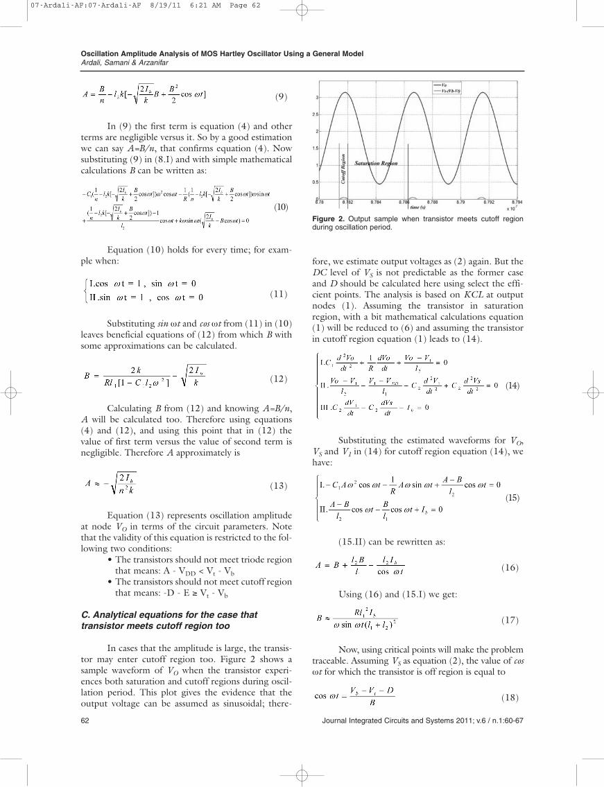
In cases that the amplitude is large, the transis-tor may enter cutoff region too. Figure 2 shows asample waveform of VO when the transistor experi-ences both saturation and cutoff regions during oscil-lation period. This plot gives the evidence that theoutput voltage can be assumed as sinusoidal; there-
(10)
fore, we estimate output voltages as (2) again. But theDC level of VS is not predictable as the former caseand D should be calculated here using select the effi-cient points. The analysis is based on KCL at outputnodes (1). Assuming the transistor in saturationregion, with a bit mathematical calculations equation(1) will be reduced to (6) and assuming the transistorin cutoff region equation (1) leads to (14).
Substituting the estimated waveforms for VO,VS and V1 in (14) for cutoff region equation (14), wehave:
(15.II) can be rewritten as:
(16)
Using (16) and (15.I) we get:
(17)
Now, using critical points will make the problemtraceable. Assuming VS as equation (2), the value of cosωt for which the transistor is off region is equal to
(18)
(15)
(14)
62 Journal Integrated Circuits and Systems 2011; v.6 / n.1:60-67
Figure 2. Output sample when transistor meets cutoff regionduring oscillation period.
07-Ardali-AF:07-Ardali-AF 8/19/11 6:21 AM Page 62

Oscillation Amplitude Analysis of MOS Hartley Oscillator Using a General ModelArdali, Samani & Arzanifar
Calculating A from (4):
(24)
Here, note that the validity of this equation isrestricted to the following a condition too:
• The transistors should not meet triode regionthat means:
D. Analytical equations for the case thattransistor meets triode region too
Most of the published methods for amplitudeanalysis in oscillators don’t have accurate analyses forthe case that transistor meets triode region during theoscillation period. Suppose that we choose VDD and Vbvalues very close to each other in configuration ofFigure 1. So, knowing that A=B/n and choosing smallvalues for n, we obtain the condition that oscillationamplitude at node VS is small but oscillation amplitudeat node VO is so large. Figure 3 and Figure 4 show asample waveform for this case. Here, the transistor willmeet saturation and triode and cutoff regions duringthe oscillation period. In this method, with the sameanalysis, analytical equations for the case that the tran-sistor meets triode region can be simply obtained. Weknow that drain current of MOS transistor in trioderegion can be expressed by this equation as follow:
(25)
The analysis proposed here is again based onthe KCL equations at output and source nodes. Theseequations can be rewritten as:
(26)
63Journal Integrated Circuits and Systems 2011; v.6 / n.1:60-67
Figure 3. Output waveforms when transistor meet triode regionduring oscillation period.
Figure 4. Sample output when the transistor meets all regionsduring oscillation period.
On the other hand, from Figure 2, we know ifωt=2nπ then VSmeets its maximum value and the tran-sistor will be exactly in cutoff region. Therefore, if (Vb- Vt - D) / B < cos ωt < 1 then the transistor will beexactly in cutoff region. One of these useful pointsoccurs on average point between two limitations, when
(19)
And
(20)
Substituting this value of cos ωt in (19) andvalue of sin ωt in (20) leads to following relationbetween B and D:
(21)
Now, we know that transistor is in cutoff regionand the time for this state is short therefore, UsingMatlab we estimate the section radical of (21) with aline as
(22)
when the transistor just remains in cutoffregion. Substituting (22) in (21), the amplitude ofsource voltage, B, is calculated. Figure 2 shows thatwhen ωt=(2n+1)π, VS reaches its minimum value, andin these points, the transistor is undoubtedly in satu-ration region. And we know that when transistor is insaturation region, D still consider by (7). Now withthese two points and substituting the equation (22) in(8.III) and using (21), we get
(23)
07-Ardali-AF:07-Ardali-AF 8/19/11 6:21 AM Page 63

Oscillation Amplitude Analysis of MOS Hartley Oscillator Using a General ModelArdali, Samani & Arzanifar
Again, assuming the output voltages as sinu-soidal waveforms makes the problem traceable. In thissection, each transistor may meet the both triode andsaturation regions during one period of oscillation.Now as the last cases, we use critical points for solvingthe problem. Choosing the points is based on knowl-edge about the times when transistor is exactly in tri-ode or saturation region. For example, when ωt=2nπ,then VO and VS are maximum as shown in Figure 3and the transistor is undoubtedly in saturation region.When ωt=(2n+1)π, VO and VS have their minimumvalue and the transistor is exactly in triode region. Onthe other hand, by the assumption of sinusoidal wave-forms for outputs, the boundary value of cos ωt atwhich the transistor maybe enters the triode region isequal to:
(27)
Therefore, if then the transistor will be in trioderegion. One of these useful points occurs when:
(28)
In this condition, transistor maybe is in allregions such as saturation and triode and cutoffregions. Again we consider D as equation (7).Therefore the equations in (26) for values of voltagesin (2) are
Again and using similar way, (29.II) can berewritten as
First for use equation (30), we have to applysome approximation in it. And substituting equation(30) in (29.I), we have
(31)
(30)
(29)
Now using value of cos ωt in (28) so the result-ed equations for these assumptions are written as (32).
And then using B and (4) A can be derivate.
Equation (33) represents oscillation amplitudeat node VO in terms of the circuit parameters when thetransistor meets all of operation regions. So this equa-tion of oscillation amplitude is considered for Hartleyoscillator in general state.
3. SIMULATIONVERSUS ANALYTICAL RESULTS
New analytical equations for amplitude analysisof MOS Hartley oscillator were presented which arebased on nonlinear differential equations of circuit.The analysis is general that involves MOS operation inall of the saturation, cutoff and triode regions. Aboveequations can be applied for synthesis of MOS Hartleyoscillator in different ways. Suppose an oscillatorwith output voltage of 1.8V has to be designedwith µnCox=275.6 x 10⁻⁵(A/V2), Vt=0.47(V) andVDD=1.8(V) where L1=6.5(nH), L2=5.5(nH),R=6(kΩ), C1=C2=0.5(pf) and Ib=200(µA). For thisoutput voltage, the transistor operates in all off thesaturation, cutoff and triode regions; furthermore, weknow n=0.542 and then B=0.542A; therefore A can becalculated from (32) as follows:
With this value for A, simulation shows -1.171V for output oscillation magnitude. As we cansee, these equations have a good agreement with sim-ulation and can be used for synthesis and hand analy-sis of MOS Hartley oscillator.
For validating our proposed equations andcomparing them with competitive methods, somesimulations and experiments are performed usingAdvanced Design System simulator (ADS). TheTSMC 0.18µm CMOS process has been used in thesesimulations. Table.I gives the details of technologysuch as supply voltage, threshold voltage and otherfeatures of the transistor that is used in circuit.
(34)
(33)
(32)
64 Journal Integrated Circuits and Systems 2011; v.6 / n.1:60-67
07-Ardali-AF:07-Ardali-AF 8/19/11 6:21 AM Page 64

Oscillation Amplitude Analysis of MOS Hartley Oscillator Using a General ModelArdali, Samani & Arzanifar
First, a typical Hartley oscillator that wasdesigned for the operation of transistor only in satura-tion region during oscillation period is presented. Ineach condition, one parameter of circuit is sweptwhereas other parameters are kept constant. The cal-culated amplitude by the proposed equation (13) iscompared with the simulation results. Figure 5 showsthe comparison between simulation and the results ofDC level of source voltage D, from our analyticalequations for the case that the transistor is only in sat-uration region during its oscillation period. In Figure(5.a) comparison is between 0.6(V) to 1.8(V) for Vbbecause the process is 0.18µm and the supply voltagecan’t become larger than 1.8(V) and the transistorneed at least 0.6(V) for it will be on. As we can see in
this figure, the results of equation (7) have a verygood agreement with simulation especially for largervoltages. In Figure (5.b) simulation and comparisonare between 0.15(mA) to 0.5(mA) for Ib. As shown inthis figure, the equation (7) for larger current hasmore accurate results.
As the last step, the circuit is simulated underdifferent conditions and parameters and comparisonsbetween simulation results and amplitude obtainedfrom the proposed method are illustrated in Figure 6,Figure 7 and Figure 8.
These simulations are repeated for the casesthat the transistor changes the operation region dur-ing oscillation period. For example, Figure 6 showsthe comparison between simulation and the resultsfrom our analytical equations for the case that thetransistor is only in saturation region during its oscil-lation period. Using Figure 6, we can select the bestvalue of n and hence l1 and l2 and also select best biascurrent Ib for better agreement with simulation. Inthis case, the transistor only is in saturation region.For example for n=0.5 we have good correspondencewith simulation. Figure 7 shows the comparison
65Journal Integrated Circuits and Systems 2011; v.6 / n.1:60-67
Table I. Details of Technology
TSMC 0.18 µmSupply Voltage 1.8 (V)
µn .Cox 275.6e-6 (A/V2)Vtn (threshold NMOS) 0.47 (V)Vtp (threshold PMOS) -0.46 (V)Transistor size (W/L) 10
Figure 5. DC value of Vs as a function of (a) Bias voltage Vb (b) Bias current Ib.
Figure 6. Comparison of simulation and analysis results when transistor meets only saturation region during oscillation period.(a) Amplitude versus n. (b) Amplitude versus Ib.
07-Ardali-AF:07-Ardali-AF 8/19/11 6:21 AM Page 65

Oscillation Amplitude Analysis of MOS Hartley Oscillator Using a General ModelArdali, Samani & Arzanifar
between simulation and the results from our analyticalequations for the case that the transistor changes itsoperation region between saturation and cutoffregions during a period of oscillation. Using Figure 7,also we can select the best value of n and we can selectbest bias current Ib. In comparison with Figure 6 inthis case, the transistor is in saturation and cutoffregions. Again, as shown in Figure 7, for n=0.5 wehave better correspondence with simulation.Therefore we can select the value of n close to the 0.5.These two figures give a good insight about n andcurrent bias Ib to design a Hartley oscillator in largeand small signal analysis.
At last, Figure 8 shows the comparisonbetween simulations and results from our analysis forthe case that the transistor operation region changesbetween saturation, triode and cutoff during oscilla-tion period. It can be performed by choosing largevalues for n, Ib and Vb to increase oscillation amplitudeat nodes VO and VS. In comparison with Figure 6 andFigure 7, in this case, the transistor is in all threeregions. These figures give an accurate insight aboutoscillation amplitude in Hartley oscillator and about
changing it as a function of circuit parameters in allstates of transistor. In our simulations, it was not pos-sible to compare our method and other proposedmethods, because they have not exact equations forthe case that the transistor meets triode region duringoscillation period and there are not any analyticalmethod for analysis amplitude oscillation in Hartleyoscillator.
4. CONCLUSION
The Hartley oscillator has been analyzed in ageneral form in which the operating region of MOStransistor may be the saturation, cutoff and trioderegions whereas previous analyses are limited only totransistor operating in saturation and cutoff regions.An analytical method to derive exact analytical equa-tions for the amplitude of Hartley oscillators has pre-sented. The output signal is assumed a sinusoidalwaveform where the unknowns are amplitude and dclevel. Applying the large signal analysis, the equationsderived in this paper represent amplitude accurately.
66 Journal Integrated Circuits and Systems 2011; v.6 / n.1:60-67
Figure 7. Comparison of simulation and analysis results when transistor changes its operation region between saturation and cutoff dur-ing oscillation period. (a) Amplitude versus n. (b) Amplitude versus Ib.
Figure 8. Comparison of simulation and analysis results when transistor changes its operation region between saturation, triode and cut-off during the oscillation period. (a) Amplitude versus n. (b) Amplitude versus Vb.
07-Ardali-AF:07-Ardali-AF 8/19/11 6:21 AM Page 66

Oscillation Amplitude Analysis of MOS Hartley Oscillator Using a General ModelArdali, Samani & Arzanifar
Nonlinear behavior of an oscillator can be explainedeasily with the presented equations. Also, the equa-tions are provided for all operation regions of transis-tors but the effect of channel length modulation andmore parasitic element are challenging points that lim-its the analysis. These equations will be of significantto be used in guiding LC oscillator design. As it canbe seen, the results from our proposed equations havegood agreement with simulation results and they canbe used for design and analysis of RF MOS Hartleyoscillator and an example illustrating this applicationwas presented.
REFERENCES
[1] E. Hegazi, J. Rael, A. Abidi, The Designer’s Guide to High-Purity Oscillators, Kluwer Academic Publishers, UnitedStates of America: 2005, ch. 4.
[2] P. M. Farahabadi, H. Miar Naimi and A. Ebrahimzadeh,“Closed Form Analytical Equations for Amplitude andFrequency of High Frequency CMOS Ring Oscillators,” IEEETrans Circuits Syst I, Vol. 56, no. 12, December 2009.
[3] Q. Huang, “Power consumption vs. LO amplitude for CMOScolpitts oscillators,” In Proc. IEEE Custom Integr. CircuitsConf, May 1997, pp255-258.
[4] K. Mayaram, “Output voltage analysis for the MOS colpittsoscillator,” IEEE Trans Circuits Syst I, Vol.47 no. 2, pp260-263, Feb.2000.
[5] M. Filanovsky, C.Verhoven and M.Reja, “Remarks onanalysis design and amplitude stability of MOS colpittsoscillator,” IEEE Trans Circuits Syst II, Vol.54, no.9, pp800-804, Sept 2007.
[6] G. Palumbo, M.Pennisi and S.Pennisi, “Approach to analyseand design nearly sinusoidal oscillators,” IET Circuits DeviseSyst., Vol.3, Issu.4, pp.204-221, August 2009.
[7] Mahmood Khatibi and Hasan Modir Shanechi, “Using modalseries to analyze the transient response of oscillators,”International journal of circuit theory and applications, DOI:10.1002/cta.515, 2009.
[8] B. Razavi, Design of Analog CMOS Integrated Circuits.McGraw Hill, New York: 2001, ch. 14.
[9] K.K. Clarke and D.T. Hess, Communication Circuits: Analysisand Design, Addison-Wesley, Reading, MA, 1971.
[10] D. O. Pederson and K. Mayaram, Analog Integrated Circuitsfor Communication: Principals, Simulation and Design.Second Edition, Springer, 2008.
[11] Shao-Hua Lee, Yun-Hsueh Chuang and Sheng-Lyang Jang,“Low-Phase Noise Hartley Differential CMOS VoltageControlled Oscillator,” IEEE microwave and wireless letters,vol. 17, no. 2, February 2007.
[12] I-Shing Shen, Tze-Che Huang, and Christina F. Jou, “A LowPhase Noise Quadrature VCO Using Symmetrical TailCurrent-Shaping Technique,” IEEE microwave and wirelesscomponents letters, Vol. 20, NO. 7, July 2010.
[13] K. Jainwal, J. Mukherjee, “Phase Noise Reduction in CMOSLC Oscillators Using Tail Noise Shaping and Gm3 Boosting,”5th International Conference on Electrical and ComputerEngineering ICECE 2008, 20-22 December 2008.
67Journal Integrated Circuits and Systems 2011; v.6 / n.1:60-67
07-Ardali-AF:07-Ardali-AF 8/19/11 6:21 AM Page 67