originally published in the proceedings of ipc works, … · the effect of filling via-in-pad on...
TRANSCRIPT
Originally published in the proceedings of IPC Works, Fort Worth, Texas, September, 2006 THE EFFECT OF FILLING VIA-IN-PAD
ON VOIDING RATES IN PWB ASSEMBLY FOR BGA COMPONENTS
Chrys Shea Rahul Raut
Lou Picchione ALPHA – A Cookson Electronics Company
Jersey City, NJ USA
Quyen Chu Nicholas Tokotch
Jabil Circuit San Jose, CA, Saint Petersburg, FL, USA
Paul Wang, Ph.D
Microsoft Corporation* Mountain View, CA, USA
ABSTRACT The debate on the effect of voiding on BGA reliability has continued for years. Many PWB assemblers strive to minimize voiding, particularly with the advent of lead-free processing and in fine feature area array devices. Although solder pastes have been designed to minimize voiding, and processing guidelines exist to mitigate void formation during reflow processing, the presence of a microvia in a PWB pad can contribute significantly to void formation. It is believed that the depression in the pad caused by the microvia traps air during the stencil printing process, and the air cannot fully escape during reflow. A process of filling the vias with copper at the board fabrication phase, thereby eliminating the depression that contributes to voids, was tested for its effectiveness in void mitigation during assembly. The test compares the voiding results of filled vias with those of unfilled vias and flat pads with no vias at all. The test vehicle and methods, as well as the results of the tests are presented and discussed in detail. KEYWORDS: BGA, Voiding, Lead-Free, Via-In-Pad, Via Fill INTRODUCTION It has long been established that voids, or small pockets of air or gas entrapped in solder joints, can present reliability concerns for any electronic product. Although there is some disagreement regarding which levels of voiding are acceptable, the consensus of the industry is typically the smaller, the better. Voiding properties are now relatively well characterized and understood, especially with tin-lead materials. The new processes and metallizations associated with lead-free processing bring new questions on voiding levels.
EXPERIMENTAL METHOD Design of Experiment A full factorial DOE was used with two replicates for each condition set. The variables were:
• Reflow profile: ramp or soak (specific to each alloy)
• PWB finish: electroless nickel/immersion gold (ENIG), immersion silver (ImAg), high temperature organic solderability preservative (OSP)
• Alloy system: tin-lead (63/37) and lead-free (SAC305)
• Via-in-pad size: 0 mil (flat pad, no via), 4 mil (100u), 6 mil (150u)
• Via fill: yes or no (for the 4 and 6 mil vias) The assembly order was not randomized due to the efficiency loss of changing over reflow recipes and solder pastes. Instead, it was blocked in the following order: paste, profile, via fill, final finish. Via size was varied on each board as part of the PWB design.

Originally published in the proceedings of IPC Works, Fort Worth, Texas, September, 2006 Materials To measure the effects of the included variables on voiding, an off-the-shelf BGA test kit was modified. The PWB artwork was updated to include High Density Interconnect outer layers, and microvias were added to the pads in some of the device footprints. The PWBs were then fabricated in one lot. The lot was divided in half prior to the conformal copper step. One half was processed with a new via filling technology. The two portions of the lot were then reunited, and conformal copper and subsequent processing steps were applied. A photograph of the test vehicle and a schematic diagram of the via layout are shown in figures 1 and 2, respectively.
Figure 1. Microvia Test Vehicle. Contains 0.5, 0.8 and 1.0mm pitch area array devices.
Figure 2. Schematic Diagram of test vehicle, devices that were populated, and the via sizes in the pads. A larger view can be seen in Appendix A. Components used in the study were:
• 0.5mm Chip Array BGA, 84 I/O • 0.8mm flexBGA, 280 I/O • 0.8mm Tape Array BGA, 144 I/O • 1.0mm Plastic BGA, 676 I/O
Components had tin-lead or SAC305 balls. Boards were assembled with matched alloys and ball materials. No mixed alloy systems were included in the study. No-clean solder pastes were used in the study. The tin-lead solder paste was ALPHA OM-5100 and the SAC305 paste was ALPHA OM-338. Assembly Method Boards were assembled on a prototype-style line in the Jersey City Applications Laboratory. The equipment set used in this study included an MPM UltraFlex 3000 stencil printer, a Universal Instruments Advantis pick and place machine, and an Electrovert OmniFlo 7-zone reflow oven with an air atmosphere. The reflow profiles are illustrated in figures 3 through 6.
Figure 3. Ramp profile for Tin-Lead alloy. Ramp rate is 0.9 C/sec. Peak temperature is 210-220 C.
Figure 4. Ramp profile for SAC305 alloy. Ramp rate is 1.2 C/sec. Peak temperature is 230-240 C.

Originally published in the proceedings of IPC Works, Fort Worth, Texas, September, 2006
Figure 5. Soak profile for Tin-Lead alloy. Soak time is 60 seconds at 160 C. Peak temperature is 210-220 C.
Figure 6. Soak profile for SAC305 alloy. Soak time is 60 seconds at 175 C. Peak temperature is 235-240 C. To minimize alignment issues, stencils were scaled to match the circuit boards’ positional accuracy. Stencil scaling is the practice of measuring the actual centroids of devices on the fabricated PWB and applying the “actual” gerber data to the stencil file before cutting.1 This practice compensates for the shrink and stretch of PWB’s that result from the fabrication process,2 and can also be used to compensate for over- or under-etch of the pads. In this experiment, the PWB’s were measured for positional accuracy and the stencil gerber was corrected. The stencil was a 5-mil foil, stepped down to 3.5 mils for the 0.5 mm devices, which had pads averaging 8.5 mil diameter, a slight overetch condition when compared with the CAD sizes of 10 mil. Aperture sizes were matched 1:1 to the pad sizes. Data Acquistion The boards were X-rayed using a next generation X-ray transmission system. The X-ray system used during inspection is capable of traditional top down perspective and also OVHM (Oblique-angle Viewing at High Magnification). The oblique angle viewing allows for the detection of void location within a solder joint, alleviates constraints due to component mirroring or occlusion, and allows for combination of multi-view calculations.
For the study, an automated program was developed that had 100% coverage, with an average test time of 10 minutes per board. The test assembly was inspected only from a top down perspective, using an existing BGA module routine. This routine measures numerous characteristics of each ball, including ball roundness, size/area, offset, gray level, voiding, and missing balls. All of the inspection criteria, including any pass/fail limits, are user definable. In this experiment, voiding percentage was of greatest interest; thus driving the inspection parameters. Due to the differing ball sizes of the components, different X-ray settings had to be used to obtain proper contrast level resolution in order to distinguish voids in the balls. The following X-ray power settings were used for the components:
• CABGA 0.5mm: 110kV 20µA • flexBGA 0.8mm: 120kV 20µA • Tape Array BGA 0.8mm: 120kV 20µA • PBGA 1.0mm: 130kV 20µA
Data Manipulation Voiding results were parsed into the following segments:
• 1-6% of joint area • 6-11% • 11-16% • 16-21% • 21-26% • 26-31% • 31-36%
Voids less than 1% were discounted for tabulation purposes. If they were counted, the algorithm that tabulates total percent of balls with voids would always result in 100%, as all the balls with 0 voids would be included in the calculation. As there is no evidence that a void of less than 1% of joint area has ever presented a reliability concern, the investigators found this to be the easiest way to tabulate the data. Furthermore, the focus of the study is mitigating the bigger voids, and in particular the influence of via-in-pad on voiding properties, which is presumed to be a controlling factor.3 For analysis purposes, the data was broken down into three groups: no vias, unfilled vias, and filled vias. Following the breakdown into these groups, the data was subsequently analyzed for the influence of some of the other variables in the experiment: alloy system and surface finish. It has been well established that soak-zone profiles are more forgiving than ramp profiles with respect to voiding because they allow time for volatiles to outgas before the alloy reaches liquidus temperatures and traps the gasses inside.4 Therefore, the ramp profile is the worst-case scenario. This worst-case scenario, or boards produced with a ramp profile, were analyzed first.

Originally published in the proceedings of IPC Works, Fort Worth, Texas, September, 2006 RESULTS AND DISCUSSION Interpreting Voiding Data Voiding results are typically reported in one of two methods: Number of balls with voids, and percent balls with voids. The number is the actual count of voids, which is often normalized as a percent for comparison among devices with differing I/O counts. In either case, the size of the voids are broken down into groups. The group sizes are based on the amount of cross-sectional area of the solder joint that the void (or voids) occupy. IPC 7095 provides guidance for Class 1, 2, and 3 performance standards by offering void size groupings. To summarize the standard, for inspection with transmission-style X-ray, the groupings are as follows:
• Class 1, voids less than 25 percent cross-sectional area
• Class 2, voids less than 12.25 percent cross-sectional area
• Class 3, voids less than 4 percent cross-sectional area For purposes of this study, it was determined that higher resolution was required in order to subsequently correlate void size with joint failure after thermal cycling. Therefore, this study uses the following void size groupings:
• 1-6 % • 6-11 % • 11-16 % • 16-21 % • 21-36 % • 31-36 %
Regardless of the breakdown into size groupings, the desired trends remain the same. Applying the popular opinion on voids that “the smaller the better and the fewer the better,” the preferred trends are groupings that lie tight against the zero point of the X-axis. This trend, shown as green lines in figure 7, indicates that the voids which are present are in the smaller size ranges. As this trend approaches the zero-point of the Y-axis, shown as broken green lines, fewer voids on the device are indicated. Again, this is the preferred condition. Conversely, a broad distribution, shown as red lines, indicates larger size voids in the device. As with the preferred distribution, the height of the curve indicates the number of voids, so the closer it lies to the zero-point of the Y-axis (broken lines), the fewer the number of voids that are present.
Frequency of Voids
0
100
200
300
400
500
1-6 6-11 11-16 16-21 21-26 26-31 31-36
Void Size, % joint area
Cou
nt o
f voi
ds, a
vera
ge p
er b
oard
Preferred Distributions
Non-Preferred Distributions
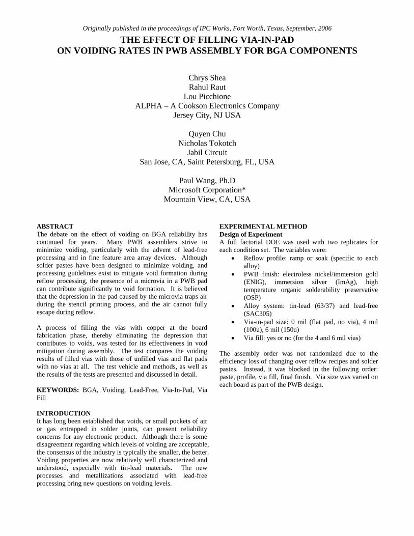
Figure 7. Typical trends found in voiding distributions. The green lines indicate smaller, fewer voids, which is considered a preferred distribution. The red lines indicate larger, more frequent voids, which is considered a non-preferred distribution. Voiding Results for all Devices Reflowed Under Ramp Profile Data has been collected and analyzed for boards processed on ramp profiles. The data presented below is the average voiding per board for 12 boards, 4 with each surface finish: high-temp OSP, ENiG, and ImAg. Two of each surface finish had vias without fill and two had vias with fill. The PWB layout allowed equal numbers of pads with and without vias for each board. Therefore, each data point for a via (filled or unfilled) is based on 6 boards, and each data point for flat pads (no via) is based on 12 boards. The number of data points depends on the I/O count of the device and the number of devices on the board, as noted in the titles of Figures 8 through 15.
Originally published in the proceedings of IPC Works, Fort Worth, Texas, September, 2006
Frequency of Voids in 0.5mm 84 I/O CABGA, Tin-Lead 504 Opportunities per assembly, min 6 assemblies per condition
0
20
40
60
80
100
120
140
160
1-6 6-11 11-16 16-21 21-26 26-31
Void Size, % solder joint area
Cou
nt o
f voi
ds, a
vera
ge p
er b
oard
Perc
ent b
alls
with
voi
ds a
nnot
ated
num
eric
ally
No Vias
4mil Via Filled
4mil Via Unfilled
7%10%
1% <1%<1%
30%27%
6%
2%<1% <1%
Figure 8. Frequency of voids in 0.5 mm 84 I/O CABGA with tin-lead alloy.
Frequency of Voids in 0.5mm 84 I/O CABGA, Lead-Free Alloy504 Opportunities per board, min 6 boards per condition
0
20
40
60
80
100
120
140
160
1-6 6-11 11-16 16-21 21-26 26-31
Void Size, % solder joint area
Cou
nt o
f voi
ds, a
vera
ge p
er b
oard
Perc
ent b
alls
with
voi
ds a
nnot
ated
num
eric
ally
No Vias
4mil Via Filled
4mil Via Unfilled
13%
8%
1%
27%
1%<1% <1%
22%
7%
7%1% 1%
Figure 9. Frequency of voids in 0.5 mm 84 I/O CABGA with lead-free alloy.
Frequency of Voids in 0.8mm 144 I/O TABGA, Tin-Lead288 Opportunities per board, 6 assemblies per condition
0
20
40
60
80
100
120
140
160
1-6 6-11 11-16 16-21 21-26 26-31
Void Size, % joint area
Cou
nt o
f voi
ds, a
vera
ge p
er b
oard
Perc
ent b
alls
with
voi
ds a
nnot
ated
num
eric
ally 4mil Via Filled
4mil Via Unfilled6mil Via Filled6mil Via Unfilled
43
5
<1
11
36
3
29
16
18
36
2
27
1824
16
74
1
Figure 10. Frequency of voids in 0.8 mm 144 I/O TABGA with tin-lead alloy.
Frequency of Voids in 0.8mm 144 I/O TABGA, Lead-Free 288 Opportunities per board, min 6 assemblies per condition
0
20
40
60
80
100
120
140
160
1-6 6-11 11-16 16-21 21-26 26-31
Void Size, % joint area
Cou
nt o
f voi
ds, a
vera
ge p
er b
oard
Perc
ent b
alls
with
voi
ds a
nnot
ated
num
eric
ally 4mil Via Filled
4mil Via Unfilled6mil Via Filled6mil Via Unfilled
38
12
2<1
43 42
19
33
14
2
22
4
<1
52
22
2
Figure 11. Frequency of voids in 0.8 mm 144 I/O TABGA with lead-free alloy.
Frequency of Voids in 0.8mm 280 I/O FLEXBGA, Tin-Lead560 Opportunities per board, minimum 6 assemblies per condition
0
50
100
150
200
250
300
1-6 6-11 11-16 16-21 21-26 < 26
Void Size, % solder joint area
Cou
nt o
f voi
ds, a
vera
ge p
er b
oard
P
erce
nt b
alls
with
voi
ds a
nnot
ated
num
eric
ally No Via
4mil Via Filled
4mil Via Unfilled
29%32%
12%
<1% 1%
31%31%
15%
6%
2%
Figure 12. Frequency of Voids in 0.8mm 280 I/O BGA with tin-lead alloy. Notice change in Y-axis scale from previous slides due to higher opportunity count.
Frequency of Voids in 0.8mm 280 I/O FLEXBGA, Lead-Free560 Opportunities per board, minimum 6 assemblies per condition
0
50
100
150
200
250
300
1-6 6-11 11-16 16-21 21-26 26-31
Void Size, % solder joint area
Cou
nt o
f voi
ds, a
vera
ge p
er b
oard
P
erce
nt b
alls
with
voi
ds a
nnot
ated
num
eric
ally No Via
4mil Via Filled
4mil Via Unfilled
25%20%
3
45
2% %
23%
6%
2%<<1 1%
Figure 13. Frequency of Voids in 0.8mm 280 I/O BGA with lead-free alloy. Notice change in Y-axis scale from previous slides due to higher opportunity count.

Originally published in the proceedings of IPC Works, Fort Worth, Texas, September, 2006
Frequency of Voids, in 1.0mm 676 I/O PBGA, Tin-Lead676 Opportunities per assembly, min 6 assemblies per condition
0
50
100
150
200
250
300
350
400
450
1-6 6-11 11-16 16-21 21-26 26-31
Void Size, % joint area
Cou
nt o
f voi
ds, a
vera
ge p
er b
oard
P
erce
nt b
alls
with
voi
ds a
nnot
ated
num
eric
ally No Via
4mil Via Filled4mil Via Unfilled
6mil Via Filled
6mil Via Unfilled
4%
64%
6%
15% 22%
40%42%
9%
<1 <1
Figure 14. Frequency of Voids in 1.0mm 676 I/O PBGA with tin-lead alloy. Again, notice a change in Y-axis scale from previous slides due to higher opportunity count.
Frequency of Voids, in 1.0mm 676 I/O PBGA, Lead-Free676 Opportunities per assembly, min 6 assemblies per condition
0
50
100
150
200
250
300
350
400
450
1-6 6-11 11-16 16-21 21-26 26-31
Void Size, % solder joint area
Cou
nt o
f Voi
ds, a
vera
ge p
er b
oard
P
erce
nt b
alls
with
voi
ds a
nnot
ated
num
eric
ally
No Via4mil Via Filled4mil Via Unfilled
6mil Via Filled6mil Via Unfilled
19%
47
17
42%
16%
<1
7%<1%8%
Figure 15. Frequency of Voids in 1.0mm 676 I/O PBGA with lead-free alloy. Again, notice a change in Y-axis scale from previous slides due to higher opportunity count.
The data presented in figures 8 through 15 has been reduced and tabulated by via size and fill, and alloy system. Within each dataset are three different PWB final finishes contributing to the overall averages that are reported. In the case of the 0.5mm CABGA, solder joints without vias and with filled 4mil vias demonstrated similar levels of voiding. Joints with unfilled vias demonstrated larger and more frequent voids. The vast majority of the voids on flat or via-filled pads are in the 1-6% of joint area size range. Voids in the pads with unfilled vias are as large as 25% of the joint and affect up to 65% of the balls. Voiding rates between tin-lead and lead-free systems appear to be similar. This similarity will be addressed with subsequent statistical analysis. The 0.8mm TABGA layout had no pads without vias. Two of the devices have 4-mil vias, and the other two have 6-mil vias. The trend among these devices is similar to the CABGAs: the filled vias (red and light blue bars) produced smaller and fewer voids than the unfilled vias. The 4-mil vias show a more favorable void distribution than the 6-mil vias. On this device, the trend of lead-free systems producing more favorable voiding properties is beginning to emerge, but again is subject to statistical verification and comparison with the other devices on the assembly. The 0.8mm FlexBGA, like the CABGA, had devices with either no vias or 4-mil vias in the pads. As anticipated, the filled vias and flat pads performed comparably, with the majority of voids in the 1-6% range and the unfilled vias producing many more, larger voids. Although the unfilled vias produced more voids than the other two condition sets, the lead-free system appears to produce a better distribution of voids and affects less joints. The tin-lead system produced voids affecting 97% of the joints while the lead-free system produced voids affecting 86% of the joints.
Comparison between the 4-mil filled vias of the tape array BGA and the FlexBGA show proportionally more voids in the tape array than the Flex. Spare devices will be x-rayed in their as-received (pre-reflow) condition to check for void contribution levels from the devices themselves. The 1.0mm PBGA was laid out with three land patterns: one with no vias, one with 4-mil vias, and one with 6-mil vias. Again, the flat pads and filled vias performed comparably, and the unfilled vias produced many more, and larger voids. When comparing the performance between tin-lead and lead-free systems, the tin-lead appeared to produce fewer voids on the flat pads and filled vias. Nearly all the voids for these configurations were in the 1-6% range. For unfilled vias, the lead-free systems clearly outperformed the tin-lead systems. Statistical analysis of the results will be performed to determine if the apparent trend of lead-free systems producing similar or less voids than tin-lead systems is significant. Further Breakdown by Surface Finish The data presented in figures 16-23 further breaks down the voiding results into individual surface finishes. The charts show the previously reviewed data, which was based on 6 assemblies, segregated by surface finish. There were two assemblies of each surface finish for each metallurgical system.

Originally published in the proceedings of IPC Works, Fort Worth, Texas, September, 2006
Void Distribution per Surface Finish, 0.5mm CABGA, Tin-Lead
504 Opportunities per assembly, min 2 assemblies per condition
0
20
40
60
80
100
120
140
160
180
200
No Via 4mil ViaFilled
4mil ViaUnfilled
No Via 4mil ViaFilled
4mil ViaUnfilled
No Via 4mil ViaFilled
4mil ViaUnfilled
Cou
nt o
f voi
ds, a
vera
ge p
er b
oard
1-6%6-11%11-16%16-21%21-26%26-31%
OSP ImAg ENiG
Figure 16. Frequency of voids separated by surface finish in 0.5mm 84 I/O CABGA in tin-lead system. Notice the performance similarities between filled vias and pads with no vias at all, and the influence of unfilled vias.
Void Distribution per Surface Finish, 0.5mm CABGALead-Free
504 Opportunities per assembly, min 2 assemblies per condition
0
20
40
60
80
100
120
140
160
180
200
No Via 4mil ViaFilled
4mil ViaUnfilled
No Via 4mil ViaFilled
4mil ViaUnfilled
No Via 4mil ViaFilled
4mil ViaUnfilled
Cou
nt o
f voi
ds, a
vera
ge p
er b
oard
1-6%6-11%11-16%16-21%21-26%
OSP ImAg ENiG
Figure 17. Frequency of voids separated by surface finish in 0.5mm 84 I/O CABGA in lead-free system. Again, notice the performance differences with respect to voiding size and occurrence.
Void Distribution per Surface Finish, 0.8mm TABGATin-Lead
288 Opportunities per assembly, 2 assemblies per condition
0
20
40
60
80
100
120
140
160
180
200
4mil ViaFilled
6mil ViaFilled
4mil ViaUnfilled
6mil ViaUnfilled
4mil ViaFilled
6mil ViaFilled
4mil ViaUnfilled
6mil ViaUnfilled
4mil ViaFilled
6mil ViaFilled
4mil ViaUnfilled
6mil ViaUnfilled
Cou
nt o
f Voi
ds, a
vera
ge p
er b
oard
1-6%6-11%11-16%16-21%21-26%
ImAgOSP ENiG
Figure 18. Voiding occurrence in 0.8mm 144 I/O TABGA with 4 and 6 mil vias in tin-lead alloy system. The unfilled vias produce larger and more frequent voids.
Void Distribution per Surface Finish, 0.8mm TABGALead-Free
288 Opportunities per assembly, 2 assemblies per condition
0
20
40
60
80
100
120
140
160
180
200
4mil ViaFilled
6mil ViaFilled
4mil ViaUnfilled
6mil ViaUnfilled
4mil ViaFilled
6mil ViaFilled
4mil ViaUnfilled
6mil ViaUnfilled
4mil ViaFilled
6mil ViaFilled
4mil ViaUnfilled
6mil ViaUnfilled
Cou
nt o
f voi
ds, a
vera
ge p
er b
oard
1-6%6-11%11-16%16-21%21-26%
OSP ENiGImAg
Figure 19. Voiding occurrence in 0.8mm 144 I/O TABGA with 4 and 6 mil vias in lead-free alloy system.
Void Distribution per Surface Finish, 0.8mm FLEXBGATin-Lead
560 opportunities per assembly, 2 assemblies per condition
0
50
100
150
200
250
300
350
400
No Via 4mil Filled 4milUnfilled
No Via 4mil Filled 4mil Unfilled
No Via 4mil Filled 4mil Unfilled
Cou
nt o
f Voi
ds, a
vera
ge p
er b
oard
1-6 %6-11 %11-16 %16-21 %21-26 %< 26%
OSP ImAg ENiG
Figure 20. Voiding occurrence in 0.8mm FlexBGA with no vias and 4 mil vias in tin-lead system. Notice a Y-axis scale change due to higher opportunity count.
Void Distribution per Surface Finish, 0.8mm FLEXBGALead-Free
560 opportunities per assembly, 2 assemblies per condition
0
50
100
150
200
250
300
350
400
No Via 4mil Filled 4mil Unfilled
No Via 4mil Filled 4mil Unfilled
No Via 4mil Filled 4mil Unfilled
Cou
nt o
f voi
ds, a
vera
ge p
er b
oard 1-6 %
6-11 %11-16 %16-21 %21-26 %< 26%
OSP ImAg ENiG
Figure 21. Voiding occurrence in 0.8mm FlexBGA with no vias and 4 mil vias in lead-free system. Notice a Y-axis scale change due to higher opportunity count.

Originally published in the proceedings of IPC Works, Fort Worth, Texas, September, 2006
Void Distribution per Surface Finish, 1.0mm PBGA Tin-Lead
676 Opportunities per assembly, 2 assemblies per condition
0
100
200
300
400
500
600
No Via 4mil Filled
6mil Filled
4mil Unfilled
6mil Unfilled
No Via 4mil Filled
6mil Filled
4mil Unfilled
6mil Unfilled
No Via 4mil Filled
6mil Filled
4mil Unfilled
6mil Unfilled
Cou
nt o
f voi
ds, a
vera
ge p
er b
oard 1-6 %
6-11 %11-16 %16-21 %21-26 %< 26%
OSP ImAg ENiG
Figure 22. Voiding occurrence in 1.0mm PBGA with no vias, 4-mil vias, and 6-mil vias. Again, the Y-axis scale has changed due to higher opportunity count. In this case, the ENIG finish appears to produce less voids than OSP or ImAg.
Void Distribution per Surface Finish, 1.0mm PBGA Lead-Free
676 Opportunities per assembly, 2 assemblies per condition
0
100
200
300
400
500
600
No Via 4mil Filled
6mil Filled
4mil Unfilled
6mil Unfilled
No Via 4mil Filled
6mil Filled
4mil Unfilled
6mil Unfilled
No Via 4mil Filled
6mil Filled
4mil Unfilled
6mil Unfilled
Cou
nt o
f voi
ds, a
vera
ge p
er b
oard
1- 6 %6-11 %11-16 %16-21 %21-26 %< 26%
OSP ImAg ENiG
Figure 23. Voiding occurrence in 1.0mm PBGA with no vias, 4-mil vias and 6-mil vias. Again, the Y-axis scale has changed due to higher opportunity count. Voiding occurrence appears similar across all finishes.
On the 0.5mm CABGA devices with 4mil vias, filled vias performed comparably to pads with no via at all. The unfilled vias produced up to 5 times as many voids as the filled vias or flat pads, with void sizes up to 26% of the solder joint area. OSP and ImAg appear to produce similar levels of voiding, with ENIG producing more voids than either the OSP or the ImAg in both tin-lead and lead-free systems. On the 0.8mm TABGA devices, the effect of via fill is clear. Pads with filled vias consistently produced joints with smaller and fewer voids. The data from the filled vias is closer to the preferred distribution, and the data from the unfilled vias more closely resembles the non-preferred distribution. As with the 0.5mm device, OSP and ImAg produced fewer voids than ENIG, and for all finishes, lead-free appears to produce less voids than tin-lead. On the 0.8mm FlexBGA devices, immersion silver appeared to produce more favorable void formation in the tin-lead system, when compared to OSP and ENIG finishes. In the lead-free system, minor (yet to be shown to be statistically significant) differences appear in the flat pad and filled via samples, but immersion silver again appears to produce more favorable voiding properties on the unfilled vias. On the 1.0mm PBGA, nearly all the voids for no via or filled vias were in the 1-6% range. Unfilled 4-mil vias produced voids no larger than the 6-11% range. These two statements apply to both alloy systems. Differentiation is seen in the 6-mil unfilled vias, where the tin-lead system produced more and larger voids than the lead-free system. This device was chosen for its large size and high I/O count which could cause large delta T’s across the package body, perhaps inducing more voids in the center of the device than in the periphery. Due to its larger ball size, however, the typical percent area void is very small. This particular device does not provide a high degree of resolution in discerning between voiding rates.
Table 1 shows the as-received (pre-reflow) nominal ball diameter and cross-sectional area.
Device Type
Ball Diameter
Ball Area
CABGA 0.3mm (12-mil)
0.07 mm2 (113 mil2)
TABGA 0.46mm (18-mil)
0.17 mm2 (255 mil2)
FlexBGA 0.46mm (18-mil)
0.17 mm2 (255 mil2)
PBGA 0.63mm (25-mil)
0.31 mm2 (490 mil2)
Table 1. Nominal BGA ball diameter and area for devices used in study. Since solder joint voids are expressed as a percentage of joint area, the same size void in two devices will present as different voiding rates. Although the diameter of the balls on the 0.8mm devices are only 50% larger than the diameter of the balls on the 0.5mm device, the cross sectional area of the joint is over 2 times as large. The 1.0 mm device’s balls are 2 times the diameter of the 0.5mm device, but the cross sectional area is 4 times as large. The data shown in this study should not be interpreted as larger devices produce smaller voids. The voids on the larger devices are smaller relative to joint size, but the voids themselves may be of the same physical dimension. CROSS SECTIONAL ANALYSIS In order to accurately represent the voiding created in this experiment, the individual datapoints for each device were reviewed. The rows whose x-ray results most closely matched the overall voiding averages for each configuration were chosen for cross sectioning. Figures

Originally published in the proceedings of IPC Works, Fort Worth, Texas, September, 2006
Figure 24. 0.5mm BGA solder joint on a flat pad (no via) with OSP finish.
Figure 25. 0.5mm BGA solder joint on a pad with a 100 micron (4 mil) microvia that has been filled, with OSP finish.
Figure 26. 0.5mm BGA solder joint on a pad with a 100 micron (4 mil) microvia that has not been filled, with OSP finish.
Figure 27. 0.5mm BGA solder joint on a pad with a 100 micron (4 mil) microvia that has not been filled, ENIG finish. 24 through 27 show cross sections of the void conditions that the investigators determined were representative of the overall results for the given condition sets.7 The first two cross sections (figures 24 and 25) show no evidence of voiding in the solder joints. On the device with no vias in the pads, 10 ball sites were examined microscopically and no voids were observed. On the devices with filled microvias in the pads, 12 ball sites were examined microscopically and no voids were observed. It is not surprising that no voids were observed during this microscopic examination. The rates of voiding for this device on OSP surface finish were: flat pads, 3.5%; filled vias, 3.9%, and the majority of the voids that were present within these devices were less than 6% of joint area. When examining 10 of the 1008 joints that were produced for each condition, where only 30 to 40 of the 1000+ joints exhibited any voiding whatsoever, finding a void in one of the cross sections would be tantamount to finding a needle in a haystack. Figure 26 shows a cross section of an unfilled via with OSP finish. In this case, 10 ball sites were examined, and all 10 sites exhibited voids. In all 10 cases, the voids were located within the via. In this configuration, 68% of the solder joints exhibited voids during X-ray analysis. Due to the minimal spread property of SACA305 alloy on copper, the molten solder never spread into the hole, and the void was not liberated into the solder joint. Figure 27 shows a similar solder joint, but with an ENIG finish on the circuit board. In this case, 12 sites were microscopically examined, all 12 sites exhibited voiding, and all the voids were observed near the top of the via. In this case, 57% of the ball sites exhibited voids during X-ray analysis. It is assumed that the improved spread of SAC305 on gold allowed the molten solder to wet into the via, liberating the void into the solder joint.

Originally published in the proceedings of IPC Works, Fort Worth, Texas, September, 2006 The location of the void is important for two reasons. The most obvious reason is the higher tolerance for voids that occur within the bulk of the joint rather than at the package or substrate interface. Less obvious, but equally as important, is the interpretation of the X-ray results. These solder joints were inspected with transmission-style, top-down X-ray views. Using this technique, it is not possible to determine whether the void was trapped in the via or liberated into the bulk of the solder joint. Therefore, one should be cautious when interpreting the X-ray data. At first glance, the results would indicate that unfilled vias on the ENIG finish produced larger voids. In reality, the voids may have the same volume. When the gas is trapped inside the cylindrical shape of the via on the OSP board, it can appear to have a smaller cross-sectional area than a void of similar volume which has been liberated into the joint and formed into a spherical shape due to surface tension properties. With the understanding of the effects of surface finish and X-ray technique, one can now compare the data for OSP and ENIG presented in figure 17 and interpret that the ENIG finish did produce larger and more frequent voids for flat pads and filled vias, but not enough information is available to support or refute similar conclusions for the unfilled vias. STATISTICAL ANALYSIS Review of the device-level voiding charts (figures 8 – 15) reveals drastically different voiding performance between unfilled vias and filled vias/flat pads, but extremely similar performance between the filled vias and flat pads. The unfilled vias were quite visibly producing higher quantities and larger voids than the other two conditions, but the performance of flat pads and filled vias was too close to judge by visual review of the graphical output. Statistical analysis was employed to compare the two conditions. The 0.5mm CABGA, 0.8mm FLEXBGA, and the 1.0mm PBGA devices all had a combination of flat pads and vias. The DOE layout allowed the 1.0mm PBGA to have both 4 and 6 mil vias; each condition was compared to flat pads. The 0.8mm TABGA did not have any flat pads in the DOE layout, so it was excluded from the statistical analysis. All PWB surface finishes are equally factored into the tests, which use the same data sets that produced figures 8-15. The first statistical test to be applied was the 2-sample t-test. In this case, the null hypothesis, i.e. voiding produced with filled vias = voiding produced on flat pads, was applied. The statistic ‘t’ was calculated based on the mean number of voids in each size cateogory. The t-value is then referenced to a p-value in a lookup table or computer software. At a 95% confidence level, the p-value must be greater than 0.05 to support the null hypothesis.
Device Type
Tin-Lead p-values
Lead-Free p-values
CABGA-No via vs 4mil filled via 0.791 0.709
FlexBGA-No via vs 4mil filled via 0.937 0.900
PBGA-No via vs 4mil filled via 0.689 0.942
PBGA-No via vs 6mil filled via 0.502 0.877
Table 2. P-values for the ‘2-sample t test’ for no via versus filled via for different devices used in study. Table 2, shows p-values from ‘2-sample t-test’ for tin-lead and lead-free components. As the p-values are greater than 0.05 the null hypothesis cannot be rejected, and it can be stated that voiding rates between filled vias and flat pads are statistically equivalent. The 2 sample t-test procedure assumes that the variances of both populations are equal. To validate this assumption, and therefore the conclusion of the t-test, the variances themselves must be analyzed. The second statistical test to be applied was the test for equal variances (2 variances). This procedure compares the variances of the two populations using calculations known as the F-test and Levene’s test, which also result in p-values. As with the t-test, p-values in the Levene’s test that are greater than 0.05 support the null hypothesis that the variances in the voiding rates between filled vias and flat pads are equal. Figures 28-35 show the results from ‘Test for equal variances (2-variances), along with its respective p-values from Levene’s test. In the graphs, the points represent the standard deviation of the each data set, and the bars represent the 95% confidence interval for these standard deviations. Overlap of the bars indicates similarity in the variances. The greater the overlap of the bars, the more similarity between variances, and the higher the resulting p-values become.

Originally published in the proceedings of IPC Works, Fort Worth, Texas, September, 2006
95% Bonferroni Confidence Intervals for StDevs
4mil Via Filled
No Vias
605040302010
Test Statistic 0.57P-Value 0.553
Test Statistic 0.07P-Value 0.795
F-Test
Levene's Test
Test for Equal Variances for 'No Vias' versus '4mil Via Filled'
Tin-Lead CABGA
Figure 28. Results of Test for equal variance’ in 0.5 mm 84 I/O CABGA with tin-lead alloy. P-values are >0.05.
95% Bonferroni Confidence Intervals for StDevs
4mil Via Filled_1
No Vias_1
706050403020100
Test Statistic 2.79P-Value 0.285
Test Statistic 0.16P-Value 0.702
F-Test
Levene's Test
Test for Equal Variances for 'No Via' versus '4mil Via Filled'
Lead-Free CABGA Figure 29. Results of ‘Test for equal variance’ in 0.5 mm 84 I/O CABGA with lead-free alloy. Again, P-values are >0.05.
95% Bonferroni Confidence Intervals for StDevs
4mil Via Filled_4
No Via
2252001751501251007550
Test Statistic 0.84P-Value 0.856
Test Statistic 0.01P-Value 0.939
F-Test
Levene's Test
Test for Equal Variances for 'No Via' versus '4mil Via Filled'
Tin-Lead FLEXBGA
Figure 30. Results for ‘Test for equal variance’ in 0.8mm 280 I/O BGA with tin-lead alloy. Again, P-values are >0.05.
95% Bonferroni Confidence Intervals for StDevs
4mil Via Filled_5
No Via_1
16014012010080604020
Test Statistic 1.55P-Value 0.644
Test Statistic 0.02P-Value 0.895
F-Test
Levene's Test
Test for Equal Variances for 'No Via' versus '4mil Via Filled'
Lead-Free FLEXBGA Figure 31. Results for ‘Test for equal variance’ in 0.8mm 280 I/O BGA with lead-free alloy. Again, P-values are >0.05.
95% Bonferroni Confidence Intervals for StDevs
4mil Via Filled_6
No Via_2
605040302010
Test Statistic 0.49P-Value 0.457
Test Statistic 0.08P-Value 0.784
F-Test
Levene's Test
Test for Equal Variances for 'No Via' versus '4mil Via Filled'
Tin-Lead PBGA
Figure 32. Results for ‘Test for equal variance’ in 1.0mm 676 I/O PBGA with tin-lead alloy. Again, P-values are >0.05.
95% Bonferroni Confidence Intervals for StDevs
4mil Via Filled_7
No Via_3
2001751501251007550
Test Statistic 1.19P-Value 0.855
Test Statistic 0.01P-Value 0.943
F-Test
Levene's Test
Test for Equal Variances for 'No Via' versus '4mil Via Filled'
Lead-Free PBGA Figure 33. Results for ‘Test for equal variance’ in 1.0mm 676 I/O PBGA with lead-free alloy. Again, P-values are >0.05.
95% Bonferroni Confidence Intervals for StDevs
6mil Via Filled_2
No Via_2
1751501251007550250
Test Statistic 0.07P-Value 0.011
Test Statistic 0.52P-Value 0.486
F-Test
Levene's Test
Test for Equal Variances for 'No Via' versus '6mil Via Filled'
Tin-Lead PBGA
Figure 34. Results for ‘Test for equal variance’ in 1.0mm 676 I/O PBGA with tin-lead alloy. Again, P-values are >0.05.
95% Bonferroni Confidence Intervals for StDevs
6mil Via Filled_3
No Via_3
20015010050
Test Statistic 1.55P-Value 0.641
Test Statistic 0.03P-Value 0.877
F-Test
Levene's Test
Test for Equal Variances for 'No Via' versus '6mil Via Filled'
Lead-Free PBGA
Figure 35. Results for ‘Test for equal variance’ in 1.0mm 676 I/O PBGA with lead-free alloy. Again, P-values are >0.05.

Originally published in the proceedings of IPC Works, Fort Worth, Texas, September, 2006 All p-values are >0.05, indicating that the variances of the compared populations are equal. The equal variances support the conclusions of the t-test, which examined the means of the voiding rates. It can therefore be stated that, with 95% confidence, the voiding rates produced on pads with filled microvias are equal to the voiding rates produced on pads with no vias at all. This is true for both tin-lead and lead-free alloy systems, on devices ranging from 0.5mm to 1.0mm pitch, and I/O counts ranging from 84 to 676. CONCLUSIONS The investigators originally set out to answer several questions as described in the abstract. The devices from half of the assemblies, or 50% of the data, have been analyzed and tabulated. Recall that all the data presented in this study is from assemblies processed on ramp-style reflow profiles, which are known to be the worst case for voiding. Based on this subset of data, the following answers are offered:
• Does lead-free solder alloy create more voids than conventional tin-lead alloy? No. Indications are that voiding rates in lead-free systems are similar or slightly less.
• How much more voiding will be expected if vias are in the pads? If the via is filled, voiding rates should not exceed those produced on pads with no vias at all. No statistically significant difference was found between the two configurations.
• Will filling the vias limit the voiding? Yes. Unfilled vias consistently produced higher quantities and larger voids than filled vias, in some cases 5 times as much. Statistical comparisons were not applied to the unfilled vias, as their large influence on void formation is obvious in simple analysis.
• What part does surface finish play in void formation? OSP and ImAg generally produced similar amounts of voids, which were less frequent and smaller than those produced with ENIG finish.
The vias were filled using a prototype of a process that has now become fully developed and commercially available. It is known as Enthone CUPROSTAR CVF-1™. Enthone is a Cookson Electronics company. COMPLETION OF STUDY Statistical analysis may be applied to the existing data to examine the significance of surface finish in void formation. If the analysis is performed, it will be published. In addition to the results already presented, the original scope of the experiment included analysis of the boards reflowed with soak profiles, thermal cycling of the assemblies, and reliability assessment. The purpose of analyzing the soak data was to differentiate voiding behavior between the two profiles as they applied to
solder paste production of voids. The purpose of thermal cycling and development of reliability models was to determine if a correlation existed between void size and reliability. At this time, the investigators are concluding the study for several reasons:
1. The voiding produced with ramp data with flat pads and filled vias was very low. The paste products used in this study were designed for low voiding properties. Other voiding studies with these paste products show that reflow profile is not a big factor in void production.
2. The recently released IPC Solder Products Value Council6 report stated “The presence of process related voids in the interconnections formed using the SAC alloys has been found to have no statistically significant effect on solder interconnection reliability as tested by accepted thermal cycling methods.” This particular study was greater in scope than the study presented in this paper. Proceeding with thermal cycling would not generate new knowledge of greater value than what is already available through the SVPC study.
3. The resources required for full execution of the original scope are better utilized by redirecting them to study some of the more pressing issues currently associated with lead-free assembly.
This study is now officially completed. The assemblies are in storage and the data has been archived. The study may be reopened in the future if deemed appropriate. Many thanks to all the contributors over the two-year span of this study. *This study is a work of collaboration from OEM, EMS, and Material Supplier, and testing Labs for knowledge sharing and facilitation of technology evolution. There is no product endorsement, business implication, and working preference in any forms are associated with this publication. Methodology proposal in this article is an experimental approach for exploiting technical insight. There is no product quality and reliability referencing implied with this approach. Application discretion is needed for other case. The information contained in this document represents the current view of Microsoft Corporation on the issues discussed as of the date of publication. Because Microsoft must respond to changing market conditions, it should not be interpreted to be a commitment on the part of Microsoft, and Microsoft cannot guarantee the accuracy of any information presented after the date of publication. This White Paper is for informational purposes only. MICROSOFT MAKES NO WARRANTIES, EXPRESS,

Originally published in the proceedings of IPC Works, Fort Worth, Texas, September, 2006 IMPLIED OR STATUTORY, AS TO THE INFORMATION IN THIS DOCUMENT. Complying with all applicable copyright laws is the responsibility of the user. Without limiting the rights under copyright, no part of this document may be reproduced, stored in or introduced into a retrieval system, or transmitted in any form or by any means (electronic, mechanical, photocopying, recording, or otherwise), or for any purpose, without the express written permission of Microsoft Corporation. Microsoft may have patents, patent applications, trademarks, copyrights, or other intellectual property rights covering subject matter in this document. Except as expressly provided in any written license agreement from Microsoft, the furnishing of this document does not give you any license to these patents, trademarks, copyrights, or other intellectual property. 2005 Microsoft Corporation. All rights reserved. Microsoft is a registered trademark of Microsoft Corporation in the United States and/or other countries. All other trademarks are property of their respective owners. REFERENCES [1] Chrys Shea, Valentijn Van Velthoven, Ron Tripp and
Ranjit S Pandher, “Reducing Variation in Outsourced SMT Manufacturing Through the use of Intelligent Stencil Systems”, Proceedings of SMTA International, September, 2003
[2] Mendez, D., Clarke,R., “Statistical Model of Printed
Wiring Board and Stencil Alignment Issues”, Proceedings of Surface Mount International Conference, April, 1997.
[3] Grano, F, et al, “Impact of Micro-Via in Pad Design on
Void Formation:, Proceedings of SMTA International, September, 2003
[4] Bruno, F, and Grano, F, et al, “Effect of Reflow Profile on
BGA Voiding in a Lead-Free Process”, Proceedings of SMTA International Conference, September, 2004
[5] ChipArray BGA & flexBGA are registered trademarks of
Amkor Technology, Inc. [6] IPC Solder products Value Council, “The Effect of
Voiding in Solder Interconnections Formed from Lead-Free Solder Pastes with Alloys of Tin, Silver, and Copper”, a Research Report by the Lead-Free Technical Subcommittee.
[7] Picchione, L. “Report of Analysis, BGA Component
Examinations for Voiding in Microvias,” CE Analytics, July, 2006.
Originally published in the proceedings of IPC Works, Fort Worth, Texas, September, 2006
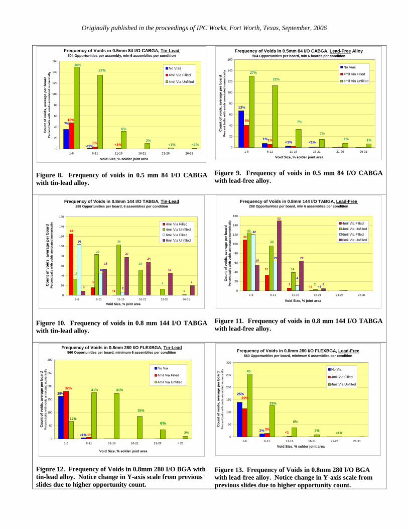
APPENDIX A Test Vehicle Layout