organic surface modification of silicon nanowire-based sensor devices
TRANSCRIPT
13
Organic Surface Modification of Silicon Nanowire-Based Sensor Devices
Louis C.P.M. de Smet1, Daniela Ullien1, Marleen Mescher1,2,3 and Ernst J.R. Sudhölter1
1Delft University of Technology, Faculty of Applied Science, Department of Chemical Engineering, Nano-Organic Chemistry,
2Materials innovation institute (M2i), 3Micro Systems and Devices, Philips Research Eindhoven,
Netherlands
1. Introduction
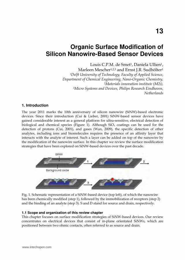
The year 2011 marks the 10th anniversary of silicon nanowire (SiNW)-based electronic devices. Since their introduction (Cui & Lieber, 2001) SiNW-based sensor devices have gained considerable interest as a general platform for ultra-sensitive, electrical detection of biological and chemical species (Figure 1). Although SiOx coatings can be used for the detection of protons (Cui, 2001), and gases (Wan, 2009), the specific detection of other analytes, including ions and biomolecules requires the presence of an affinity layer that interacts with the analyte of interest. Such a layer can be added on top of the nanowire by the modification of the nanowire surface. In this chapter we review the surface modification strategies that have been explored on SiNW-based devices over the past decade.
Fig. 1. Schematic representation of a SiNW-based device (top left), of which the nanowire has been chemically modified (step 1), followed by the immobilization of receptors (step 2) and the binding of an analyte (step 3). S and D stand for source and drain, respectively.
1.1 Scope and organization of this review chapter This chapter focuses on surface modification strategies of SiNW-based devices. Our review concentrates on electrical devices that consist of in-plane orientated SiNWs, which are positioned between two ohmic contacts, often referred to as source and drain.
www.intechopen.com

Nanowires - Implementations and Applications
268
For an extensive overview of different materials that have been explored to prepare NW-based sensors, including silicon, we refer to the review of Ramgir et al. (Ramgir, 2010). Several reviews on SiNW-based devices have been written with a clear focus on the chemical-vapour-deposition fabricated NWs by the Lieber and Zhou groups (Li, 2006; Patolsky, 2006b; Carlen & van den Berg, 2007) or top–down fabricated SiNW-based sensors from the Reed group (Stern, 2008). In this chapter we will discuss issues related to the modification of SiNW-based devices with organic compounds. The topics of SiOx (Aswal, 2006) and Si-H (Aswal, 2006; Stutzmann, 2006; Hamers, 2008) surface modification with covalently linked organic monolayers have been reviewed extensively. However, the main focus of these reviews is on the modification of large planar substrates, while the focus if this chapter is on SiNW-based devices. A review by Wanekaya et al. contains a paragraph on the covalent functionalization of SiNWs with biomolecules (Wanekaya, 2006). Very recent reviews also include sections with brief schemes for SiNW functionalization (Shao, 2010; Tey, 2010). In this chapter we aim to give an overview of all the different surface modification strategies that have been explored to modify SiNW-based devices, including non-covalent immobilization strategies. The methods can be divided into different categories (Table 1). The first one is based on silanization chemistry, i.e., the reaction between hydroxyl-terminated surfaces and organosilanes. Also other compounds like activated esters or organophosphonates have been covalently attached to SiOx surfaces. In addition, polyelectrolytes and bilayers have been physically adsorbed onto SiOx surfaces. The last
approach follows the route of oxide removal, followed by the reaction with (ω-functionalized)-1-alkenes.
Surface Modification
Method Type of Binding
Nature Film# Papers
(Year of First Report)
§
SiOx Silanization Covalent Monolayer >50 (2001) 2.1.1
SiOx Esterification Covalent Monolayer 1 (2004) 2.2
SiOx Phosphorization Covalent Monolayer 1 (2008) 2.2
SiOx Layer-by-Layer Electrostatic Multilayers 1 (2010) 2.3.1
SiOx Lipid membrane Electrostatic Bilayer 2 (2009) 2.3.2
Si-H Hydrosilylation Covalent Monolayer 6 (2006) 3
Table 1. Overview of different strategies used in the modification of SiNW-based devices.
2. SiOx-covered SiNW-based sensor devices
Cleaned silicon surfaces exposed in an ambient environment such as air or solutions will oxidize spontaneously (Zhang, 2001b). The silicon oxide layer, in this chapter referred to as SiOx –either native oxide or oxide grown under controlled conditions–, passivates the silicon surface. This allows the silicon to be used as an electronic material in processing and application environments. After fabrication, or at least after exposure to ambient environment, also SiNWs contain a SiOx layer. Typically the thickness of this SiOx layer on the NW is 1.5-10 nm, whereas the background oxide is usually >10 nm. It is important to note that –in terms of surface modification– one cannot discriminate between the oxide of the nanowire and background oxide; both are modified. The surface modifications described in §2 deal with SiOx-coated SiNW devices.
www.intechopen.com

Organic Surface Modification of Silicon Nanowire-Based Sensor Devices
269
2.1 Covalent functionalization 2.1.1 Silanization The most applied method to functionalize silica surfaces is through the self-assembly of
organofunctional alkoxysilane and chlorosilane molecules. While early silane-based
monolayer work is based on Langmuir-Blodgett techniques, the first silane-based self-
assembled monolayer was reported by Sagiv in 1980 (Sagiv, 1980). In general, a
hydroxylated surface is introduced into a solution of a silane derivative in an organic
solvent, but gas-phase methods have also been used (Aswal, 2006). In all cases, thorough
cleaning of the substrate is a must for obtaining a clean and activated (hydroxylated) oxide
layer with a high density of silanol groups on the surface (~ 1015 per cm2) (Aswal, 2006).
Scheme 1 gives a schematic representation of the formation of a silane monolayer onto SiOx
surfaces. It should be noted that this chemistry is not limited to SiOx surfaces; other
hydroxylated oxides surfaces can be modified as well (e.g., Al2O3 (Wang, 2008)).
Also in the case of the surface functionalization of the SiOx surfaces of SiNW-based devices
the most applied method is silanization. Figure 2 gives an overview of the different silane
derivatives that have been used, while Table 2 gives a number of examples of surface
silanization, together with the target analytes. It should be noted that on planar SiOx
substrates more compounds have been used; here we aim to give an overview for
SiNW-based devices only. Table 2 summarizes the first papers on SiNW-based sensor
devices and selected papers that use other silanization methods. We have categorized the
references in terms of pH sensors, biosensors, cation sensors and gas sensors. This way,
the cited work does not only represent the diversity of silane compounds that have
been used, it also shows the variation in the further (bio)functionalization of SiNW-based
devices.
Scheme 1. Schematic representation of the 1) cleaning/hydroxylation of the SiOx surface, 2)
silanization (here: silane 1a, Figure 2), and 3) further functionalization with glutaraldehyde.
It should be noted that the exact structure of the bonded silanes is arbitrary as also two or
three silanol groups per attached molecule may react with the surface hydroxyl groups.
Here we adapted the scheme from Aswal et al. (Aswal, 2006).
www.intechopen.com

Nanowires - Implementations and Applications
270
Sensor Type
Surface Modification*
Receptor Analyte Reference
pH
SiO2 H+
APTES (1a) H+ (Cui, 2001;
Bunimovich, 2006; Chen, 2006)
APTES (1a) DNA-templated
polymerization of aniline
H+ (Ma, 2004)
Bio `
Biotin Streptavidin (Cui, 2001)
APTES (1a) 15-mer ss-DNA
Hybridization-induced charges
in poly-T/poly-A 15-mer DNA
(Lin, 2007)
APDMES (1b) 16-mer ss-DNA Complementary
DNA (Bunimovich,
2006)
MPTMS (4a) 12-mer ss-DNA Single mismatch (Li, 2004)
APMS (3) Monoclonal antibodies PSA (Zheng, 2005)
APMS (3) Antibody influenza (Patolsky, 2004)
APMS (3) Tyrosine kinase ATP (Wang, 2005)
APTES (1a) GA Estrogen receptors
protein
Estrogen response elements
(Zhang, 2010)
APTES (1a) GA Anti-PSA PSA (Kim, 2007)
APTES** (1a) GA Glucose oxidase Glucose (Wang, 2008)
APTES (1a) GA Anti-CRP CRP (Lobert, 2003;
Patolsky, 2006a)
APTES (1a) EDC-supported
carboxy-phenylboronic acid (CPBA)
Dopamine (Li, 2010)
AEAPS (2) Gold nanoparticles Thiol-terminated
enzyme (Sheu, 2005)
Cations
SiO2 Calmodulin Ca2+ (Cui, 2001)
MPTES (4b) Hg+, Cd+ (Luo, 2009)
AEAPS (2) GA (phosphor)tyrosine Ca2+ (Bi, 2008b)
APMS (3) Gly-Gly-His Cu2+ (Bi, 2008a)
Gas APTES (1a) TNT (Engel, 2010)
Table 2. Examples of surface modifications on SiOx-covered SiNW devices and target analytes.
GA = Glutaraldehyde; EDC = 1-Ethyl-3-[3-dimethylaminopropyl]carbodiimide hydrochloride; PSA = Prostate specific antigen; ATP = Adenosine triphosphate; TNT = Trinitrotoluene; CRP = C-reactive protein; * The chemical structures of the silanes are given in Figure 2; ** The silicon nanowires are covered with a layer of 10 nm Al2O3, grown by atomic layer deposition.
www.intechopen.com

Organic Surface Modification of Silicon Nanowire-Based Sensor Devices
271
Fig. 2. Compounds that have been used in the modification on SiOx-coated NWs in NW-based devices: 3-aminopropyltriethoxysilane (APTES, 1a), (3-aminopropyl)-dimethyl-ethoxysilane (APDMES, 1b), N-(2-aminoethyl)-3-aminopropyltrimethoxysilane (AEAPS, 2), 3-aldehydepropyltrimethoxysilane (APMS, 3), mercaptopropyltrimethoxysilane (MPTMS, 4a), mercaptopropyltriethoxysilane (MPTES, 4b), biotin 4-nitrophenyl ester (BNPE, 5) and 11-hydroxyundecyl-phosphonate (HUP, 6).
2.1.1.1 3-Aminopropyltriethoxysilane
The first paper of the Lieber group on SiNW-based devices shows the utilization of silane-based functionalization of SiOx-coated nanowires (Cui, 2001). The devices were chemically modified with 3-aminopropyltriethoxysilane (APTES, Figure 2, silane 1a). The resulting devices showed a linear source-drain conductance versus pH-response for pH values from 2 to 9. The authors explained these results by the presence of both NH3+ and SiOH groups, which have different acid dissociation constants. At low pH, the amino group is protonated, and acts as a positive gate, which depletes hole carriers in the p-type SiNW and decreases the conductance. At high pH, the SiOH group is deprotonated, causing an increase in conductance. Ma et al. realized pH sensitivity via the enzymatic polymerization of aniline, which was templated by DNA on APTES (Ma, 2004) (Figure 3). The direct use of the stretched, immobilized DNA molecules as templates prevents the agglomeration of the polyaniline/DNA complexes formed in solution.
Fig. 3. Fabrication of a polyaniline nanowire immobilized on a SiOx surface with stretched double-stranded DNA as a guiding template, resulting in pH sensitivity. HRP stands for horseradish peroxidase. Figure from (Ma, 2004) reprinted with permission from the American Chemical Society ©.
www.intechopen.com

Nanowires - Implementations and Applications
272
Besides its use as sensitive layer in the detection of protons, recently APTES has also been used as a sensing layer for the vapor-phase detection of 2,4,6-trinitrotoluene (TNT) (Engel, 2010). The sensing mechanism is based on the acid-base interaction between the amino-terminated nanowire surface and the polarized TNT nitro groups, which have a weak basicity. The binding of electron-deficient TNT molecules to the amino groups on the SiNW sensor surface is believed to result in the formation of charge-transfer complexes, which act as effective molecular gating elements. The conductance response of the resulting devices has a clear relation with the concentration of the explosive analytes and the device was found to be able to distinguish the target analyte from structurally related compounds. This example nicely shows that SiNW-based sensors are not only sensitive to changes in charges, but also to changes in charge density. Given its reactivity towards aldehyde, carboxylic acid and epoxy functionalities, APTES has become the most frequently used linker compound for further (bio)functionalization of SiNWs. The activation procedure of the SiOx nanowire surface using an oxygen plasma, followed by the immersion in a solution of APTES in ethanol and subsequent heating of the chip as reported by the Lieber group (Cui, 2001) is commonly used (Patolsky, 2006a; Wang, 2008). Alternative approaches have been reported as well, e.g., the use of UV/ozone for the surface activation, followed by the use of neat APTES (Li, 2010). Also toluene (Lobert, 2003) and acetone (Lin, 2007) have been used as a solvent in the silanization step. Because of the possibility of hydrogen bond formation between the amine of APTES and the SiOx surface, both head and tail groups can be oriented towards the surface, which can result in a large disorder in APTES layers (Vandenberg, 1991). Additionally, cross-linking between the alkoxy silane units may yield oligomerized silane structures on the surface, resulting in rough layers that are thicker than a monolayer. The optimal conditions for solvent-based silanization using APTES were investigated on planar surfaces (Howarter & Youngblood, 2006). The morphology and growth kinetics of APTES films deposited from solutions were found to be affected by reaction time, solution concentration, and temperature. Experiments with an APTES concentration of 1% only produced good films when the reaction was time-limited (1 h). Increasing the reaction time increased the APTES film thickness. To overcome the problem of the disordered monolayers, Lin et al. performed a post-treatment of APTES-functionalized devices (Lin, 2007). After the APTES modification, they aligned the internal dipoles of the APTES molecules using high electric fields, thus decreasing the disorder in the monolayer. In addition, it is shown that the source-drain conductance of the APTES-functionalized devices changes upon UV illumination. The authors explained this by a strengthening effect of the internal APTES dipoles by UV illumination. Additionally, UV illumination excites extra charge carriers in the nanowire. Depending on the size of both effects, the resistance of the nanowire can be increased or decreased, which was found to be measurable with the produced devices. A modification that often follows the attachment of APTES to the SiOx nanowire surface is the reaction with glutaraldehyde (GA, Scheme 1, right). This linker molecule is used to form an aldehyde-terminated surface, which increases the possibilities for further reactions, including the reaction with amine groups of, e.g., anti-bodies (Kim, 2007), proteins and enzymes (Lee, 2008; Wang, 2008; Zhang, 2010). Also amino-terminated, single-stranded DNA (ss-DNA) has been attached to APTES/GA-modified surfaces to measure hybridization-induced mismatches in 15-mer ss-DNA chains (Lin, 2007). The addition of glutaraldehyde is, like that of APTES, both performed from solution (Bi, 2008b; Zhang, 2010) and from the gas phase (Wang, 2008).
www.intechopen.com
Organic Surface Modification of Silicon Nanowire-Based Sensor Devices
273
Li et al. reported the functionalization of an APTES-coated thin oxide gate with a dopamine receptor (Li, 2010). Although the devices do no belong to the class of SiNW-based sensors, the CMOS open-gate Field-Effect Transistor (FET) devices have (sub)micrometer gate dimensions. They have immobilized carboxyphenylboronic acid onto the APTES layer. The boronic acid group specifically reacts with the catechol functionality of, e.g., dopamine, which was detected in the femtomolar range.
2.1.1.2 Other silane derivatives
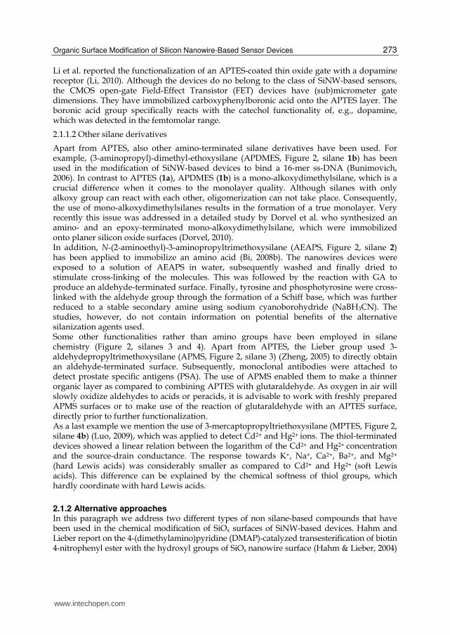
Apart from APTES, also other amino-terminated silane derivatives have been used. For example, (3-aminopropyl)-dimethyl-ethoxysilane (APDMES, Figure 2, silane 1b) has been used in the modification of SiNW-based devices to bind a 16-mer ss-DNA (Bunimovich, 2006). In contrast to APTES (1a), APDMES (1b) is a mono-alkoxydimethylsilane, which is a crucial difference when it comes to the monolayer quality. Although silanes with only alkoxy group can react with each other, oligomerization can not take place. Consequently, the use of mono-alkoxydimethylsilanes results in the formation of a true monolayer. Very recently this issue was addressed in a detailed study by Dorvel et al. who synthesized an amino- and an epoxy-terminated mono-alkoxydimethylsilane, which were immobilized onto planer silicon oxide surfaces (Dorvel, 2010). In addition, N-(2-aminoethyl)-3-aminopropyltrimethoxysilane (AEAPS, Figure 2, silane 2) has been applied to immobilize an amino acid (Bi, 2008b). The nanowires devices were exposed to a solution of AEAPS in water, subsequently washed and finally dried to stimulate cross-linking of the molecules. This was followed by the reaction with GA to produce an aldehyde-terminated surface. Finally, tyrosine and phosphotyrosine were cross-linked with the aldehyde group through the formation of a Schiff base, which was further reduced to a stable secondary amine using sodium cyanoborohydride (NaBH3CN). The studies, however, do not contain information on potential benefits of the alternative silanization agents used. Some other functionalities rather than amino groups have been employed in silane chemistry (Figure 2, silanes 3 and 4). Apart from APTES, the Lieber group used 3-aldehydepropyltrimethoxysilane (APMS, Figure 2, silane 3) (Zheng, 2005) to directly obtain an aldehyde-terminated surface. Subsequently, monoclonal antibodies were attached to detect prostate specific antigens (PSA). The use of APMS enabled them to make a thinner organic layer as compared to combining APTES with glutaraldehyde. As oxygen in air will slowly oxidize aldehydes to acids or peracids, it is advisable to work with freshly prepared APMS surfaces or to make use of the reaction of glutaraldehyde with an APTES surface, directly prior to further functionalization. As a last example we mention the use of 3-mercaptopropyltriethoxysilane (MPTES, Figure 2, silane 4b) (Luo, 2009), which was applied to detect Cd2+ and Hg2+ ions. The thiol-terminated devices showed a linear relation between the logarithm of the Cd2+ and Hg2+ concentration and the source-drain conductance. The response towards K+, Na+, Ca2+, Ba2+, and Mg2+ (hard Lewis acids) was considerably smaller as compared to Cd2+ and Hg2+ (soft Lewis acids). This difference can be explained by the chemical softness of thiol groups, which hardly coordinate with hard Lewis acids.
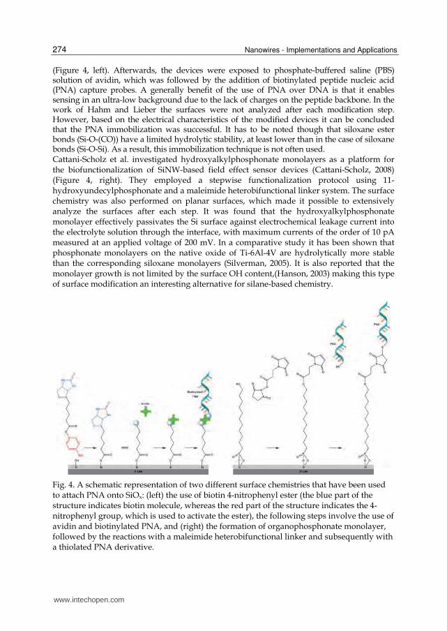
2.1.2 Alternative approaches In this paragraph we address two different types of non silane-based compounds that have been used in the chemical modification of SiOx surfaces of SiNW-based devices. Hahm and Lieber report on the 4-(dimethylamino)pyridine (DMAP)-catalyzed transesterification of biotin 4-nitrophenyl ester with the hydroxyl groups of SiOx nanowire surface (Hahm & Lieber, 2004)
www.intechopen.com
Nanowires - Implementations and Applications
274
(Figure 4, left). Afterwards, the devices were exposed to phosphate-buffered saline (PBS) solution of avidin, which was followed by the addition of biotinylated peptide nucleic acid (PNA) capture probes. A generally benefit of the use of PNA over DNA is that it enables sensing in an ultra-low background due to the lack of charges on the peptide backbone. In the work of Hahm and Lieber the surfaces were not analyzed after each modification step. However, based on the electrical characteristics of the modified devices it can be concluded that the PNA immobilization was successful. It has to be noted though that siloxane ester bonds (Si-O-(CO)) have a limited hydrolytic stability, at least lower than in the case of siloxane bonds (Si-O-Si). As a result, this immobilization technique is not often used. Cattani-Scholz et al. investigated hydroxyalkylphosphonate monolayers as a platform for the biofunctionalization of SiNW-based field effect sensor devices (Cattani-Scholz, 2008) (Figure 4, right). They employed a stepwise functionalization protocol using 11-hydroxyundecylphosphonate and a maleimide heterobifunctional linker system. The surface chemistry was also performed on planar surfaces, which made it possible to extensively analyze the surfaces after each step. It was found that the hydroxyalkylphosphonate monolayer effectively passivates the Si surface against electrochemical leakage current into the electrolyte solution through the interface, with maximum currents of the order of 10 pA measured at an applied voltage of 200 mV. In a comparative study it has been shown that phosphonate monolayers on the native oxide of Ti-6Al-4V are hydrolytically more stable than the corresponding siloxane monolayers (Silverman, 2005). It is also reported that the monolayer growth is not limited by the surface OH content,(Hanson, 2003) making this type of surface modification an interesting alternative for silane-based chemistry.
Fig. 4. A schematic representation of two different surface chemistries that have been used to attach PNA onto SiOx: (left) the use of biotin 4-nitrophenyl ester (the blue part of the structure indicates biotin molecule, whereas the red part of the structure indicates the 4-nitrophenyl group, which is used to activate the ester), the following steps involve the use of avidin and biotinylated PNA, and (right) the formation of organophosphonate monolayer, followed by the reactions with a maleimide heterobifunctional linker and subsequently with a thiolated PNA derivative.
www.intechopen.com

Organic Surface Modification of Silicon Nanowire-Based Sensor Devices
275
2.2 Non-covalent functionalization 2.2.1 Adsorption of polyelectrolytes The negative nature of SiOx at pH > 3.5 allows one to electrostatically immobilize positively charged polymers (polycations), also called generally polyelectrolytes (PEs). Subsequently, a negatively charged polymer (polyanion) can be adsorbed on top. Providing that each adsorption step of charged polymers leads to a charge inversion of the surface (charge overcompensation effect), the subsequent deposition finally results in a PE multilayer, stabilized by strong, multivalent electrostatic forces. This method is known as layer-by-layer (LbL) deposition (Decher, 1997). A variety of deposition methods can be used, including dip-coating, spin-coating, spray-coating and flow-based techniques. Recently Ingebrandt and coworkers applied the LbL deposition technology onto SiNW-based devices (Vu, 2010). They immobilized polyallylamine hydrochloride (PAH: MW 15,000) onto 6 nm thick, thermally grown SiOx via dip coating. Subsequently, polystyrenesulphonate (PSS: MW 60,000-80,000) was immobilized and this sequence was repeated several times to make a stack of 6 bilayers (Figure 5). The thickness of the resulting multilayer has not been reported. Assuming a monolayer thickness of ~ 2 nm (Decher, 1997; Poghossian, 2007) the multistack thickness would be ~ 24 nm. It has to be noted, however, that the salt concentration has an effect on the layer thickness (Decher & Schmitt, 1992), which makes it difficult to predict the thickness accurately. Although the noise level of PE-coated devices was slightly higher than that of their standard FET devices, the sensitivity for PE adsorption measurements was 3 to 4 times higher as compared to previous reports.
Fig. 5. Structures of the polycation polyallylamine hydrochloride (PAH) and polyanion polystyrenesulphonate (PSS) used by Ingebrandt and coworkers to prepare layer-by-layer multilayers onto SiOx-covered SiNW-based devices.
2.2.2 Lipid membranes Silica surfaces have also been used as a platform to immobilize model membrane systems like supported lipid bilayers, which have been extensively used in understanding the fundamental properties of biological membranes. However, there have been only a few attempts to apply lipid membranes on nanoelectronic devices. Misra et al. incorporated lipid bilayer membranes into SiNW transistors (Figure 6). In more detail, they covered the NWs and the background oxide with a continuous lipid bilayer shell, forming a barrier between the SiOx surface and solution species (Martinez, 2009; Misra, 2009). The method is based on the fusion of spherical unilamellar vesicles onto a SiNW surface producing a planar conformal lipid bilayer coating (Huang, 2007).
www.intechopen.com

Nanowires - Implementations and Applications
276
Fig. 6. Device schematics showing a SiNW connected to microfabricated source (S) and drain (D) electrodes. Although this is not clear from the figure it should be noted that the source and drain are insulated with Si3N4. The insets show the configuration of the lipid bilayer and a pore channel placed in the bilayer membrane. Figure from (Misra, 2009) reprinted with permission from National Academy of Sciences, USA.
Cyclic voltammetry using potassium ferrocyanide (K4Fe(CN)6) as a redox probe showed that the presence of a lipid bilayer on the NW surface reduced the limiting current by 85–95% relative to the native oxide-covered NW device (Misra, 2009). Subsequently, two different transmembrane peptides (gramicidin A and alamethicin) were incorporated in the vesicles, resulting in ion channel-containing lipid bilayers after fusion with SiNW-based devices. It was shown that the incorporation of transmembrane peptide pores enabled ionic-to electronic-signal-transduction by using voltage-gated and chemically gated ion transport through the membrane pores.
3. Oxide-free SiNW-based sensor devices
3.1 Hydrosilylation As an alternative to silane-based chemistry, silicon substrates can also be modified using so-called hydrosilylation chemistry, e.g., the reaction between a surface Si-H and an organic compound containing a terminal unsaturated carbon-carbon bond (alkenes and alkynes) to form a Si-C linked monolayer (Scheme 2).
Scheme 2. Schematic representation of the 1) etching of the SiOx surface, yielding a H-terminated surface, 2) formation of Si-C monolayers via hydrosilylation (R1 represents a functional group that is chemically protected towards the reaction with the H-terminated Si surface, e.g., an ester or amide), 3) deprotection the functional group (represented by R2, e.g., a carboxylic acid or amine), 4) attachment of a receptor (represented by R3).
This work has been pioneered by Linford and Chidsey in the early 1990s (Linford & Chidsey, 1993; Linford, 1995) and this type of monolayers has continued to attract attention ever since. Hydrosilylation chemistry requires removal of SiOx, which in most cases is achieved using wet chemistry. On planar silicon surfaces diluted, aqueous HF and NH4F solutions are used to etch Si(100) and Si(111) substrates, respectively, although a wide variety of etching methods has become available (Zhang, 2001a). This process results in
www.intechopen.com

Organic Surface Modification of Silicon Nanowire-Based Sensor Devices
277
hydrogen-terminated, oxide-free silicon substrates with Si-H groups. The reaction of H-terminated silicon surfaces with alkenes and alkynes can be performed by making use of high temperatures, UV and visible light irradiation, electrochemistry, hydrosilylation catalysts (e.g., AlCl3), and chemomechanical scribing, as summarized in different reviews (Buriak, 2002; Stutzmann, 2006; Hamers, 2008; Ciampi, 2010).
3.2 Organic monolayers: Si-C versus SiOx-C Si-C bonded monolayers have a number of advantages over silane-based monolayers on SiOx surfaces. First, interface trap densities for Si-C bonded monolayers can be considered remarkably lower than in the case of alkyl chains organic monolayers on naturally oxidized silicon surfaces (Kar, 2001). Also, as already mentioned in §2.1.1.1, silane oligomerization can result in rough layers that are thicker than a monolayer. In contrast, the reaction between a H-terminated Si surface and alkenes or alkynes results in a true monolayer. This is related to the involved zipper mechanism, in which each binding of an alkyl chain directly generates a new radical site on the next-nearest Si surface atom (Linford, 1995). Moreover, the chemical stability of monolayers on SiOx in aqueous media is poor since the exposure to water pilots the destruction of the monolayer through hydrolysis of Si-O bonds (Calistri-Yeh, 1996). Organic layers formed by hydrosilylation are stable in a number of environments, including air, boiling water, organic solvents, and acids (Linford, 1995). In the field of SiNW-based devices, the application of Si-C monolayers has a number of
other benefits as compared to silane-based surface modifications. First, the removal of SiOx
brings a sensing event (target/analyte interaction) closer to the conducting surface, which
increases the sensitivity of the device (Bunimovich, 2006; Zhang, 2008a). Second, the
selective functionalization of oxide-free SiNWs is considered to be a supplementary factor
that improves the detection sensitivity by avoiding the binding competition between the
SiNW and the oxide surface on the rest of the device. Third, several studies show improved
electrical properties of Si-C linked monolayers over monolayers on SiOx, in terms of the flat-
band potential and source-drain conductance (Faber, 2005b; Vilan, 2010).
A crucial difference between the silane-based and alkene-based approach becomes clear
from, e.g., the preparation of amine-terminated monolayers. While in the case of SiOx
unprotected amines can be used (§2.1.1), e.g., APTES, amine-containing alkenes should be
chemically protected as amines can react with H-terminated Si surfaces. The N-tert-
butoxycarbonyl (t-BOC, Figure 7, alkenes 7a and 7b) is a commonly used protecting group
for primary amines, but other protecting groups have been used as well (Sieval, 2001a).
Apart from amines, also carboxylic acid and alcohol functionalities should be protected
before application in the hydrosilylation chemistry (Buriak, 2002).
Characteristic of Si-C bonded monolayers is that the molecular cross-section of the attached
alkyl chain prevents reaction of all individual Si–H bonds, i.e., upon formation of a
monolayer on Si(111) about 50-55% of the Si–H sites has reacted (Sieval, 2001b), while on
Si(100) this is about 30-35% (Sieval, 2000a). The remaining, unreacted Si-H sites are a
potential source for the formation of interface states, e.g., via oxidation, which is an
unfavourable process in terms of device performance.
3.3 Hydrosilylation on SiNW-based sensor devices The reported chemistry for functionalizing the oxide-free, H-terminated SiNW sensor devices is limited to one method, i.e., hydrosilylation catalyzed by UV irradiation. This
www.intechopen.com

Nanowires - Implementations and Applications
278
approach has been applied by different research groups using different etching conditions and probing different types of analytes (Table 3). The first report on the modification of oxide-free SiNW-based devices is by Heath and
coworkers (Bunimovich, 2006). The authors followed an established, multistep protocol
(Bunimovich, 2004; Streifer, 2005) that starts with the hydrosilylation of H-terminated
SiNWs with tert-butyl allylcarbamate (Figure 7, alkene 7a) irradiated at 254 nm. After
deprotection, the researchers obtained a positively charged amine-terminated monolayer on
the SiNWs, enabling the adsorption of negatively charged, oligo ss-DNA.
Surface characterization of the nanowires embedded in a device is a challenge, since
conventional analytical tools used for surface characterization require substrates on the
micro-scale. For that reason a widely used strategy is to perform the applied chemistry also
on planar samples.
Analyte Receptor Alkene* Oxide Etching Conditions Reference
ss-DNA ss-DNA 7a native 2% HFaq (3 s) (Bunimovich, 2006)
K+, Na+ Crown Ether
7b 5-10 nm 1% HFaq (50 s) +
NH4Faq (60 s) (Zhang, 2007)
ss-DNA ss-PNA 7b ~ 5 nm 1% HFaq (50 s) +
NH4Faq (60 s) (Zhang, 2008a; Zhang,
2008b)
Avidin/ Streptavidin
Biotin 7b not
reported
10:1 v/v 40% NH4Faq/ 49% HFaq (5
s) (Stern, 2007)
Antigen Antibody 7b
- - 8, 9
Table 3. Overview of the references that report on the chemical modification of the SiNW-based devices via hydrosilylation chemistry.
* The chemical structures of the alkenes are given in Figure 7.
Fig. 7. Alkene derivatives that have been chemically bound to oxide-free SiNW sensor devices. The protecting groups on various alkenes are marked in dashed rectangles. For alkene 7a and 7b the protecting group is N-tert-butoxycarbonyl (t-BOC), for alkene 8 it is the tetrahydropyranyl (THP) group. See text for further information.
www.intechopen.com

Organic Surface Modification of Silicon Nanowire-Based Sensor Devices
279
This strategy was also followed by Bunimovich et al. and planar Si(100) samples were analyzed by water contact angle measurements and X-ray Photoelectron Spectroscopy. Moreover, this interesting paper compares Si-C and SiOx-based monolayers. It is shown that the electrical read-out of oxide-free SiNWs for sensing complementary 16-mer DNA was more profound than on modified, SiOx-covered SiNWs. Also Zhang et al. used hydrosilylation chemistry to coat SiNW devices with ss-DNA, although a different strategy was chosen (Zhang, 2008a; Zhang, 2008b). The modification scheme starts with the UV-initiated attachment of 10-N-boc-amino-dec-1-ene (Figure 7, alkene 7b) to a device with H-terminated SiNWs. After the deprotection of the amino groups the surface was chemically modified with glutaraldehyde, allowing the covalent binding of amino-terminated compounds. Inspired by the work of others on devices with SiOx nanowires (Strother, 2000; Hahm & Lieber, 2004; Bi, 2008a), they subsequently immobilized PNA. The benefit of this approach over the method reported by Bunimovich et al. is twofold: PNA is not only neutral (see also §2.1.2), it is also bonded covalently. Although multivalent, ionic interactions might be stronger than one single covalent bond, the latter is independent of the salt concentration, making it more robust in wide range of chemically different environments. As for sample characterization the research group was quite successful in depicting the chemistry performed on the SiNWs. Transmission electron microscopy (TEM) was performed for a morphological study of the non-oxidized SiNW surface. From the TEM data the authors concluded that the surface was nearly uniform, oxide free and did not show visible TEM-detectable defects (Figure 8b). In addition, binding of fluorescently labeled, complementary DNA was used to demonstrate the selectivity of the non-oxidized SiNW surface chemistry and the specificity of PNA-DNA hybridization. Indeed, strong fluorescent signals on the SiNWs were obtained and the bright arrays of SiNWs were clearly visible (Figure 8c).
Fig. 8. Cross-sectional TEM micrographs of SiNWs before and after HF and NH4F etching: (a) SiOx layer coated on the SiNW surface prior to etching, (b) hydrogen-terminated SiNW after etching, (c) Fluorescent images of Cy3-labeled complementary DNA hybridized to the PNA-functionalized SiNWs. The inset shows SEM micrograph of SiNW arrays. Figure from (Zhang, 2008a) reprinted with permission from Elsevier.
Earlier work by Zhang et al. focused on the sensing of alkali metal ions by the chemical
modification of SiNW-based devices with crown ethers (Zhang, 2007). Also in this case
alkene 7b was used, followed by the reaction with glutaraldehyde, resulting in an aldehyde-
terminated monolayer. Subsequently, amine-terminated crown ethers were covalently
attached. Based on the complexation selectivity of crown ethers to alkali metal ions, the
resulting functionalized oxide-free SiNW-based devices could detect Na+ and K+.
(c)
www.intechopen.com
Nanowires - Implementations and Applications
280
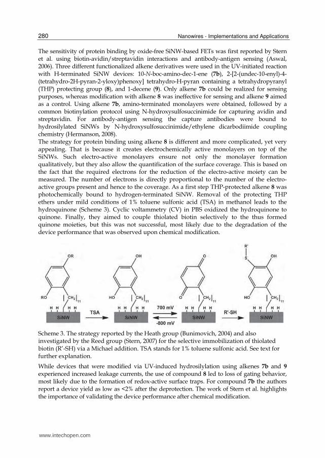
The sensitivity of protein binding by oxide-free SiNW-based FETs was first reported by Stern et al. using biotin-avidin/streptavidin interactions and antibody-antigen sensing (Aswal, 2006). Three different functionalized alkene derivatives were used in the UV-initiated reaction with H-terminated SiNW devices: 10-N-boc-amino-dec-1-ene (7b), 2-[2-(undec-10-enyl)-4-(tetrahydro-2H-pyran-2-yloxy)phenoxy] tetrahydro-H-pyran containing a tetrahydropyranyl (THP) protecting group (8), and 1-decene (9). Only alkene 7b could be realized for sensing purposes, whereas modification with alkene 8 was ineffective for sensing and alkene 9 aimed as a control. Using alkene 7b, amino-terminated monolayers were obtained, followed by a common biotinylation protocol using N-hydroxysulfosuccinimide for capturing avidin and streptavidin. For antibody-antigen sensing the capture antibodies were bound to hydrosilylated SiNWs by N-hydroxysulfosuccinimide/ethylene dicarbodiimide coupling chemistry (Hermanson, 2008). The strategy for protein binding using alkene 8 is different and more complicated, yet very appealing. That is because it creates electrochemically active monolayers on top of the SiNWs. Such electro-active monolayers ensure not only the monolayer formation qualitatively, but they also allow the quantification of the surface coverage. This is based on the fact that the required electrons for the reduction of the electro-active moiety can be measured. The number of electrons is directly proportional to the number of the electro-active groups present and hence to the coverage. As a first step THP-protected alkene 8 was photochemically bound to hydrogen-terminated SiNW. Removal of the protecting THP ethers under mild conditions of 1% toluene sulfonic acid (TSA) in methanol leads to the hydroquinone (Scheme 3). Cyclic voltammetry (CV) in PBS oxidized the hydroquinone to quinone. Finally, they aimed to couple thiolated biotin selectively to the thus formed quinone moieties, but this was not successful, most likely due to the degradation of the device performance that was observed upon chemical modification.
Scheme 3. The strategy reported by the Heath group (Bunimovich, 2004) and also investigated by the Reed group (Stern, 2007) for the selective immobilization of thiolated biotin (R’-SH) via a Michael addition. TSA stands for 1% toluene sulfonic acid. See text for further explanation.
While devices that were modified via UV-induced hydrosilylation using alkenes 7b and 9 experienced increased leakage currents, the use of compound 8 led to loss of gating behavior, most likely due to the formation of redox-active surface traps. For compound 7b the authors report a device yield as low as <2% after the deprotection. The work of Stern et al. highlights the importance of validating the device performance after chemical modification.
www.intechopen.com

Organic Surface Modification of Silicon Nanowire-Based Sensor Devices
281
3.4 Organic monolayers on oxide-free SiNW devices: towards sensing The observation of changes in device performance upon chemical modification of its sensing area has not only been reported by Stern et al., but also in a few other cases. Yet there is evidence that even non-charged molecules adsorbed on the nanowire alter the device characteristics. Haick et al. showed an improved conductance of the H-terminated SiNWs upon the chlorination/alkylation of the nanowire (Haick, 2006). They reported that methyl-terminated SiNWs exhibit higher source-drain conductance values, lower surface defect levels and higher on-off ratios than oxygenated SiNWs. Another example of characterizing the surface passivation of a NW prior to sensing is the work of Masood et al. (Masood, 2010). An improved device behavior after hydrosilylation on SiNW with 1-octadecene has been shown by means of capacitance-voltage and current-front-gate voltage electrical measurements. Based on other studies showing that hydrogen-terminated Si(111) surfaces have the lowest reported surface recombination velocity and improved electronic performance as compared to Si(100) surfaces with SiO2 interfaces, the authors stress the importance of using Si(111) surface to further improve the Si-NW biosensor performance.
4. Concluding remarks and outlook
In order to bind (bio)receptor molecules onto SiNW-based devices, most studies apply the silanization on the nanowire oxide layer. Clearly APTES is the most frequently used silane-based agent, enabling the subsequent immobilization of carboxylic acid- or aldehyde-terminated biomolecules. More often, further derivativization with glutaraldehyde has been applied to chemically bind amine-terminated biomolecules. A disadvantage of silane compounds is their ability to react with each other via cross-linking of the alkoxy units, resulting in rough, unordered multilayers. Based on the optimization studies on planar silica substrates that have become available (Howarter & Youngblood, 2006) and reports on the quality differences between vapour- and wet chemistry-prepared APTES layers (Fiorilli, 2008), there is room for the improvement of silane chemistry on SiNW-based devices. Phosphonate monolayers are an interesting alternative for silane-based monolayers, due to their higher hydrolytical stability and the less critical pretreatment of the oxide surface that is required. Apart from covalent functionalization of SiNW-based sensor devices also physisorption has been studied, which enabled the detection of several compounds and ions. Covalent attachment of (bio)molecules to sensor surfaces may be appealing in terms of device stability, but some systems, e.g., membrane receptors require a more dynamic environment. It has been shown that a phospholipid monolayer can be covalently immobilized on SiOx (Heysel, 1995) and Si-H (Charrier, 2010) surfaces, enabling the non-covalent immobilization of a second phospholipid layer. However, this strategy may hamper the fluidic properties of the bilayer, which is vital for the incorporation of biologically active structures into the membrane. The fusion of spherical unilamellar vesicles onto surfaces overcomes this problem. So far, only two different transmembrane ion channels on SiNW-based devices have been reported (Misra, 2009), but lipid bilayers provide a matrix for a virtually unlimited number of transmembrane proteins that can accommodate different functionalities. Physisorbed PE layers are not covalently attached; nevertheless they are very stable, due to the multivalent character of the interaction. The multivalency is also beneficial
www.intechopen.com

Nanowires - Implementations and Applications
282
regarding the detection of a PEs that adsorbs onto the SiNW-based device. LbL films of PE have been employed for various applications, including electrochemical sensing and biosensing and they have also contributed to the investigation of fundamental studies in electrochemistry (Crespilho, 2006). The work of Ingebrandt and coworkers (Vu, 2010) can now be extended to the use of biologically relevant PEs and perhaps also the incorporation of nanoparticles. An interesting candidate to replace SiOx layers on silicon surfaces is found in alkene-prepared organic monolayers. There are a number of benefits for monolayers on oxide-free silicon over silane-based layers: a) no risk of oligomerization, resulting in a true monolayer, b) higher chemical stability, c) selective functionalization, i.e., the background surface is not functionalized, and d) a lower density of interface traps. Although a wide variety of preparation procedures for hydrosilylation surface chemistry are available, so far only UV-initiated methods have been used in the chemical modification of oxide-free H-terminated SiNW devices. This can be explained by the fact that the research in this direction is still in its early days, and it probably will not take long before some of the other available preparation methods will be explored on SiNW-based devices. An important issue in this regard is the surface orientation of the nanowire (Bunimovich, 2004). In addition, a very good monolayer quality is needed, reducing the number of interfacial defects (Seitz, 2006). In contrast to SiOx-covered SiNW-based devices, the insulating properties in the case of oxide-free SiNW-based devices are exclusively to be realized by the organic monolayer itself. One possibility to improve the monolayer quality is by using alkynes instead of alkenes (Sieval, 2000b; Faber, 2005a; Scheres, 2010). To conclude, selective functionalization of the nanowires is critical to retain sensitivity as the modification of the background oxide results in a reduced sensitivity. In addition, the modification of individual nanowires that are part of a larger array is essential to perform a multi-analysis using a single device. Continued advances in the preparation of well-defined, defect-free, organic-semiconductor interfaces will further improve the performance of SiNW-based devices. The combination of an increasingly growing number of interesting (bio)receptors, sophisticated device fabrication methods, improved electrical characterization procedures and advanced organic surface modification does not only provide unlimited research opportunities, it will also contribute significantly to diverse, highly usable sensor applications in a variety of fields.
5. Acknowledgment
This research was supported by the Dutch Technology Foundation STW, the Materials innovation institute M2i and by a VENI grant from the Netherlands Organization for Scientific Research (NWO) to LCPMdS.
6. References
Aswal, D. K., S. Lenfant, D. Guerin, J. V. Yakhmi and D. Vuillaume (2006). Self assembled
monolayers on silicon for molecular electronics. Analytica Chimica Acta 568(1-2), 84-
108.
Bi, X. Y., A. Agarwal, N. Balasubramanian and K. L. Yang (2008a). Tripeptide-modified
silicon nanowire based field-effect transistors as real-time copper ion sensors.
Electrochemistry Communications 10(12), 1868-1871.
www.intechopen.com
Organic Surface Modification of Silicon Nanowire-Based Sensor Devices
283
Bi, X. Y., W. L. Wong, W. J. Ji, A. Agarwal, N. Balasubramanian and K. L. Yang (2008b).
Development of electrochemical calcium sensors by using silicon nanowires
modified with phosphotyrosine. Biosensors & Bioelectronics 23(10), 1442-1448.
Bunimovich, Y. L., G. L. Ge, K. C. Beverly, R. S. Ries, L. Hood and J. R. Heath (2004).
Electrochemically programmed, spatially selective biofunctionalization of silicon
wires. Langmuir 20(24), 10630-10638.
Bunimovich, Y. L., Y. S. Shin, W. S. Yeo, M. Amori, G. Kwong and J. R. Heath (2006).
Quantitative real-time measurements of DNA hybridization with alkylated
nonoxidized silicon nanowires in electrolyte solution. Journal of the American
Chemical Society 128(50), 16323-16331.
Buriak, J. M. (2002). Organometallic chemistry on silicon and germanium surfaces. Chemical
Reviews 102(5), 1271-1308.
Calistri-Yeh, M., E. J. Kramer, R. Sharma, W. Zhao, M. H. Rafailovich, J. Sokolov and J. D.
Brock (1996). Thermal stability of self-assembled monolayers from
alkylchlorosilanes. Langmuir 12(11), 2747-2755.
Carlen, E. T. and A. van den Berg (2007). Nanowire electrochemical sensors: can we live
without labels? Lab on a Chip 7(1), 19-23.
Cattani-Scholz, A., D. Pedone, M. Dubey, S. Neppl, B. Nickel, P. Feulner, J. Schwartz, G.
Abstreiter and M. Tornow (2008). Organophosphonate-based PNA-
functionalization of silicon nanowires for label-free DNA detection. ACS Nano 2(8),
1653-1660.
Charrier, A., T. Mischki and G. P. Lopinski (2010). Direct stabilization of a phospholipid
monolayer on H-terminated silicon. Langmuir 26(4), 2538-2543.
Chen, Y., X. H. Wang, S. Erramilli, P. Mohanty and A. Kalinowski (2006). Silicon-based
nanoelectronic field-effect pH sensor with local gate control. Applied Physics Letters
89(22), 223512
Ciampi, S., J. B. Harper and J. J. Gooding (2010). Wet chemical routes to the assembly of
organic monolayers on silicon surfaces via the formation of Si-C bonds: surface
preparation, passivation and functionalization. Chemical Society Reviews 39(6), 2158-
2183.
Crespilho, F. N., V. Zucolotto, O. N. Oliveira Jr. and F. C. Nart (2006). Electrochemistry of
Layer-by-Layer Films: a review. Int. J. Electrochem. Sci. 1, 194-214.
Cui, Y. and C. M. Lieber (2001). Functional nanoscale electronic devices assembled using
silicon nanowire building blocks. Science 291(5505), 851-853.
Cui, Y., Q. Q. Wei, H. K. Park and C. M. Lieber (2001). Nanowire nanosensors for highly
sensitive and selective detection of biological and chemical species. Science
293(5533), 1289-1292.
Decher, G. (1997). Fuzzy nanoassemblies: toward layered polymeric multicomposites.
Science 277(5330), 1232-1237.
Decher, G. and J. Schmitt (1992). Fine-tuning of the film thickness of ultrathin multilayer
films composed of consecutively alternating layers of anionic and cationic
polyelectrolytes. Progr. Colloid Polym. Sci. 89, 160-164.
www.intechopen.com

Nanowires - Implementations and Applications
284
Engel, Y., R. Elnathan, A. Pevzner, G. Davidi, E. Flaxer and F. Patolsky (2010).
Supersensitive detection of explosives by silicon nanowire arrays. Angewandte
Chemie-International Edition 49(38), 6830-6835.
Faber, E. J., L. C. P. M. de Smet, W. Olthuis, H. Zuilhof, E. J. R. Sudhölter, P. Bergveld and
A. van den Berg (2005a). Covalently attached 1-alkynes on silicon surfaces
provide superious insulators. SAFE 2005, 8th Annual Workshop on Circuits,
Systems and Signal Processing, Veldhoven, the Netherlands November 17-18,
2005.
Faber, E. J., L. C. P. M. de Smet, W. Olthuis, H. Zuilhof, E. J. R. Sudhölter, P. Bergveld and A.
van den Berg (2005b). Si-C linked organic monolayers on crystalline silicon surfaces
as alternative gate insulators. ChemPhysChem 6(10), 2153-2166.
Fiorilli, S., P. Rivolo, E. Descrovi, C. Ricciardi, L. Pasquardini, L. Lunelli, L. Vanzetti, C.
Pederzolli, B. Onida and E. Garrone (2008). Vapor-phase self-assembled
monolayers of aminosilane on plasma-activated silicon substrates. Journal of Colloid
and Interface Science 321(1), 235-241.
Hahm, J. and C. M. Lieber (2004). Direct ultrasensitive electrical detection of DNA
and DNA sequence variations using nanowire nanosensors. Nano Letters 4(1), 51-
54.
Haick, H., P. T. Hurley, A. I. Hochbaum, P. D. Yang and N. S. Lewis (2006). Electrical
characteristics and chemical stability of non-oxidized, methyl-terminated silicon
nanowires. Journal of the American Chemical Society 128, 8990-8991.
Hamers, R. J. (2008). Formation and characterization of organic monolayers on
semiconductor surfaces. Annual Review of Analytical Chemistry 1, 707-736.
Hanson, E. L., J. Schwartz, B. Nickel, N. Koch and M. F. Danisman (2003). Bonding self-
assembled, compact organophosphonate monolayers to the native oxide surface of
silicon. Journal of the American Chemical Society 125(51), 16074-16080.
Hermanson, G. T. (2008). Bioconjugate Techniques (2nd Edition), Elsevier Science &
Technology Books, ISBN 0123705010, New York, Chapter 11.
Heysel, S., H. Vogel, M. Sanger and H. Sigrist (1995). Covalent attachment of functionalized
lipid bilayers to planar wave-guides for measuring protein-binding to biomimetic
membranes. Protein Science 4(12), 2532-2544.
Howarter, J. A. and J. P. Youngblood (2006). Optimization of silica silanization by 3-
aminopropyltriethoxysilane. Langmuir 22(26), 11142-11147.
Huang, S. C. J., A. B. Artyukhin, J. A. Martinez, D. J. Sirbuly, Y. Wang, J. W. Ju, P. Stroeve
and A. Noy (2007). Formation, stability, and mobility of one-dimensional lipid
Bilayers on polysilicon nanowires. Nano Letters 7, 3355-3359.
Kar, S., C. Miramond and D. Vuillaume (2001). Properties of electronic traps at silicon/1-
octadecene interfaces. Applied Physics Letters 78(9), 1288-1290.
Kim, A., C. S. Ah, H. Y. Yu, J. H. Yang, I. B. Baek, C. G. Ahn, C. W. Park, M. S. Jun and S. Lee
(2007). Ultrasensitive, label-free, and real-time immunodetection using silicon field-
effect transistors. Applied Physics Letters 91(10), 103901.
Lee, M. H., K. N. Lee, S. W. Jung, W. H. Kim, K. S. Shin and W. K. Seong (2008). Quantitative
measurements of C-reactive protein using silicon nanowire arrays. International
Journal of Nanomedicine 3(1), 117-124.
www.intechopen.com

Organic Surface Modification of Silicon Nanowire-Based Sensor Devices
285
Li, D. C., P. H. Yang and M. S. C. Lu (2010). CMOS open-gate ion-sensitive Field-Effect
Transistors for ultrasensitive dopamine detection. IEEE Transactions on Electron
Devices 57(10), 2761-2767.
Li, Y., F. Qian, J. Xiang and C. M. Lieber (2006). Nanowire electronic and optoelectronic
devices. Materials Today 9(10), 18-27.
Li, Z., Y. Chen, X. Li, T. I. Kamins, K. Nauka and R. S. Williams (2004). Sequence-specific
label-free DNA sensors based on silicon nanowires. Nano Letters 4(2), 245-247.
Lin, M. C., C. J. Chu, L. C. Tsai, H. Y. Lin, C. S. Wu, Y. P. Wu, Y. N. Wu, D. B. Shieh, Y. W. Su
and C. D. Chen (2007). Control and detection of organosilane polarization on
nanowire field-effect transistors. Nano Letters 7(12), 3656-3661.
Linford, M. R. and C. E. D. Chidsey (1993). Alkyl monolayers covalently bonded to silicon
surfaces. Journal of the American Chemical Society 115(26), 12631-12632.
Linford, M. R., P. Fenter, P. M. Eisenberger and C. E. D. Chidsey (1995). Alkyl monolayers
on silicon prepared from 1-alkenes and hydrogen-terminated silicon. Journal of the
American Chemical Society 117(11), 3145-3155.
Lobert, P. E., D. Bourgeois, R. Pampin, A. Akheyar, L. M. Hagelsieb, D. Flandre and J.
Remacle (2003). Immobilization of DNA on CMOS compatible materials. Sensors
and Actuators B-Chemical 92(1-2), 90-97.
Luo, L. B., J. S. Jie, W. F. Zhang, Z. B. He, J. X. Wang, G. D. Yuan, W. J. Zhang, L. C. M. Wu
and S. T. Lee (2009). Silicon nanowire sensors for Hg2+ and Cd2+ ions. Applied
Physics Letters 94(19), 3.
Ma, Y., J. Zhang, G. Zhang and H. He (2004). Polyaniline nanowires on Si surfaces
fabricated with DNA templates. Journal of the American Chemical Society 126(22),
7097-7101.
Martinez, J. A., N. Misra, Y. M. Wang, P. Stroeve, C. P. Grigoropoulos and A. Noy (2009).
Highly efficient biocompatible single silicon nanowire electrodes with functional
biological pore channels. Nano Letters 9(3), 1121-1126.
Masood, M. N., S. Chen, E. T. Carlen and A. v. d. Berg (2010). All-(111) surface silicon
nanowires: selective functionalization for biosensing applications. ACS Applied
Materials & Interfaces 2(12), 3422-3428.
Misra, N., J. A. Martinez, S. C. J. Huang, Y. M. Wang, P. Stroeve, C. P. Grigoropoulos and A.
Noy (2009). Bioelectronic silicon nanowire devices using functional membrane
proteins. Proceedings of the National Academy of Sciences of the United States of America
106(33), 13780-13784.
Patolsky, F., G. F. Zheng, O. Hayden, M. Lakadamyali, X. W. Zhuang and C. M. Lieber
(2004). Electrical detection of single viruses. Proceedings of the National Academy of
Sciences of the United States of America 101(39), 14017-14022.
Patolsky, F., G. F. Zheng and C. M. Lieber (2006a). Fabrication of silicon nanowire devices
for ultrasensitive, label-free, real-time detection of biological and chemical species.
Nature Protocols 1(4), 1711-1724.
Patolsky, F., G. F. Zheng and C. M. Lieber (2006b). Nanowire-based biosensors. Analytical
Chemistry 78(13), 4260-4269.
Poghossian, A., M. H. Abouzar, F. Amberger, D. Mayer, Y. Han, S. Ingebrandt, A.
Offenhausser and M. J. Schoning (2007). Field-effect sensors with charged
www.intechopen.com

Nanowires - Implementations and Applications
286
macromolecules: Characterisation by capacitance-voltage, constant-capacitance,
impedance spectroscopy and atomic-force microscopy methods. Biosensors &
Bioelectronics 22(9-10), 2100-2107.
Ramgir, N. S., Y. Yang and M. Zacharias (2010). Nanowire-based sensors. Small 6(16), 1705-
1722.
Sagiv, J. (1980). Organized monolayers by adsorption.1. Formation and structure of
oleophobic mixed monolayers on solid-surfaces. Journal of the American Chemical
Society 102(1), 92-98.
Scheres, L., M. Giesbers and H. Zuilhof (2010). Self-assembly of organic monolayers onto
hydrogen-terminated silicon: 1-alkynes are better than 1-alkenes. Langmuir 26(13),
10924-10929.
Seitz, O., T. Bocking, A. Salomon, J. J. Gooding and D. Cahen (2006). Importance of
monolayer quality for interpreting current transport through organic molecules:
Alkyls on oxide-free Si. Langmuir 22(16), 6915-6922.
Shao, M. W., D. D. D. Ma and S. T. Lee (2010). Silicon nanowires - synthesis, properties, and
applications. European Journal of Inorganic Chemistry(27), 4264-4278.
Sheu, J. T., C. C. Chen, P. C. Huang, Y. K. Lee and M. L. Hsu (2005). Selective deposition of
gold nanoparticles on SiO2/Si nanowires for molecule detection. Japanese Journal of
Applied Physics Part 1-Regular Papers Brief Communications & Review Papers 44(4B),
2864-2867.
Sieval, A. B., R. Linke, G. Heij, G. Meijer, H. Zuilhof and E. J. R. Sudhölter (2001a). Amino-
terminated organic monolayers on hydrogen-terminated silicon surfaces. Langmuir
17(24), 7554-7559.
Sieval, A. B., R. Linke, H. Zuilhof and E. J. R. Sudhölter (2000a). High-quality alkyl
monolayers on silicon surfaces. Advanced Materials 12(19), 1457-1460.
Sieval, A. B., R. Opitz, H. P. A. Maas, M. G. Schoeman, G. Meijer, F. J. Vergeldt, H. Zuilhof
and E. J. R. Sudhölter (2000b). Monolayers of 1-alkynes on the H-terminated Si(100)
surface. Langmuir 16(26), 10359-10368.
Sieval, A. B., B. van den Hout, H. Zuilhof and E. J. R. Sudhölter (2001b). Molecular modeling
of covalently attached alkyl monolayers an the hydrogen-terminated Si(111)
surface. Langmuir 17(7), 2172-2181.
Silverman, B. M., K. A. Wieghaus and J. Schwartz (2005). Comparative properties of siloxane
vs phosphonate monolayers on a key titanium alloy. Langmuir 21(1), 225-228.
Stern, E., J. F. Klemic, D. A. Routenberg, P. N. Wyrembak, D. B. Turner-Evans, A. D.
Hamilton, D. A. LaVan, T. M. Fahmy and M. A. Reed (2007). Label-free
immunodetection with CMOS-compatible semiconducting nanowires. Nature
445(7127), 519-522.
Stern, E., A. Vacic and M. A. Reed (2008). Semiconducting nanowire field-effect transistor
biomolecular sensors. IEEE Transactions on Electron Devices 55(11), 3119-3130.
Streifer, J. A., H. Kim, B. M. Nichols and R. J. Hamers (2005). Covalent functionalization and
biomolecular recognition properties of DNA-modified silicon nanowires.
Nanotechnology 16(9), 1868-1873.
www.intechopen.com

Organic Surface Modification of Silicon Nanowire-Based Sensor Devices
287
Strother, T., R. J. Hamers and L. M. Smith (2000). Covalent attachment of
oligodeoxyribonucleotides to amine-modified Si (001) surfaces. Nucleic Acids
Research 28(18), 3535-3541.
Stutzmann, M., J. A. Garrido, M. Eickhoff and M. S. Brandt (2006). Direct
biofunctionalization of semiconductors: A survey. Physica Status Solidi a-
Applications and Materials Science 203(14), 3424-3437.
Tey, J. N., I. P. M. Wijaya, J. Wei, I. Rodriguez and S. G. Mhaisalkar (2010). Nanotubes-
/nanowires-based, microfluidic-integrated transistors for detecting biomolecules.
Microfluidics and Nanofluidics 9(6), 1185-1214.
Vandenberg, E. T., L. Bertilsson, B. Liedberg, K. Uvdal, R. Erlandsson, H. Elwing and I.
Lundstrom (1991). Structure of 3-aminopropyl triethoxy silane on silicon-oxide.
Journal of Colloid and Interface Science 147(1), 103-118.
Vilan, A., O. Yaffe, A. Biller, A. Salomon, A. Kahn and D. Cahen (2010). Molecules on Si:
electronics with chemistry. Advanced Materials 22(2), 140-159.
Vu, X. T., R. Stockmann, B. Wolfrum, A. Offenhaesser and S. Ingebrandt (2010).
Fabrication and application of a microfluidic-embedded silicon nanowire
biosensor chip. Physica Status Solidi a-Applications and Materials Science 207(4), 850-
857.
Wan, J., S. R. Deng, R. Yang, Z. Shu, B. R. Lu, S. Q. Xie, Y. F. Chen, E. Huq, R. Liu and X. P.
Qu (2009). Silicon nanowire sensor for gas detection fabricated by nanoimprint on
SU8/SiO2/PMMA trilayer. Microelectronic Engineering 86(4-6), 1238-1242.
Wanekaya, A. K., W. Chen, N. V. Myung and A. Mulchandani (2006). Nanowire-based
electrochemical biosensors. Electroanalysis 18(6), 533-550.
Wang, W. U., C. Chen, K. H. Lin, Y. Fang and C. M. Lieber (2005). Label-free detection of
small-molecule-protein interactions by using nanowire nanosensors. Proceedings
of the National Academy of Sciences of the United States of America 102(9), 3208-
3212.
Wang, X. H., Y. Chen, K. A. Gibney, S. Erramilli and P. Mohanty (2008). Silicon-based
nanochannel glucose sensor. Applied Physics Letters 92(1), 013903.
Zhang, G. J., A. Agarwal, K. D. Buddharaju, N. Singh and Z. Q. Gao (2007). Highly sensitive
sensors for alkali metal ions based on complementary-metal-oxide-semiconductor-
compatible silicon nanowires. Applied Physics Letters 90(23), 233903.
Zhang, G. J., J. H. Chua, R. E. Chee, A. Agarwal, S. M. Wong, K. D. Buddharaju and N.
Balasubramanian (2008a). Highly sensitive measurements of PNA-DNA
hybridization using oxide-etched silicon nanowire biosensors. Biosensors &
Bioelectronics 23(11), 1701-1707.
Zhang, G. J., M. J. Huang, Z. H. H. Luo, G. K. I. Tay, E. J. A. Lim, E. T. Liu and J. S. Thomsen
(2010). Highly sensitive and reversible silicon nanowire biosensor to study nuclear
hormone receptor protein and response element DNA interactions. Biosensors &
Bioelectronics 26(2), 365-370.
Zhang, G. J., G. Zhang, J. H. Chua, R. E. Chee, E. H. Wong, A. Agarwal, K. D. Buddharaju,
N. Singh, Z. Q. Gao and N. Balasubramanian (2008b). DNA sensing by silicon
nanowire: charge layer distance dependence. Nano Letters 8(4), 1066-1070.
www.intechopen.com

Nanowires - Implementations and Applications
288
Zhang, X. G. (2001). Electrochemistry of Silicon and its Oxide, Kluwer Academic/ Plenum
Publishers, 0-306-46541-8, New York, Chapter 2.
Zheng, G. F., F. Patolsky, Y. Cui, W. U. Wang and C. M. Lieber (2005). Multiplexed electrical
detection of cancer markers with nanowire sensor arrays. Nature Biotechnology
23(10), 1294-1301.
www.intechopen.com

Nanowires - Implementations and ApplicationsEdited by Dr. Abbass Hashim
ISBN 978-953-307-318-7Hard cover, 538 pagesPublisher InTechPublished online 18, July, 2011Published in print edition July, 2011
InTech EuropeUniversity Campus STeP Ri Slavka Krautzeka 83/A 51000 Rijeka, Croatia Phone: +385 (51) 770 447 Fax: +385 (51) 686 166www.intechopen.com
InTech ChinaUnit 405, Office Block, Hotel Equatorial Shanghai No.65, Yan An Road (West), Shanghai, 200040, China
Phone: +86-21-62489820 Fax: +86-21-62489821
This potentially unique work offers various approaches on the implementation of nanowires. As it is widelyknown, nanotechnology presents the control of matter at the nanoscale and nanodimensions within fewnanometers, whereas this exclusive phenomenon enables us to determine novel applications. This bookpresents an overview of recent and current nanowire application and implementation research worldwide. Weexamine methods of nanowire synthesis, types of materials used, and applications associated with nanowireresearch. Wide surveys of global activities in nanowire research are presented, as well.
How to referenceIn order to correctly reference this scholarly work, feel free to copy and paste the following:
Ernst Sudholter, Louis De Smet, Marleen Mescher and Daniela Uliien (2011). Organic Surface Modification ofSilicon Nanowire-Based Sensor Devices, Nanowires - Implementations and Applications, Dr. Abbass Hashim(Ed.), ISBN: 978-953-307-318-7, InTech, Available from: http://www.intechopen.com/books/nanowires-implementations-and-applications/organic-surface-modification-of-silicon-nanowire-based-sensor-devices

© 2011 The Author(s). Licensee IntechOpen. This chapter is distributedunder the terms of the Creative Commons Attribution-NonCommercial-ShareAlike-3.0 License, which permits use, distribution and reproduction fornon-commercial purposes, provided the original is properly cited andderivative works building on this content are distributed under the samelicense.