organic memory tutorial vs2 - university of exeter...
TRANSCRIPT

The Microelectronics Training Center, IMEC v.z.w.www.imec.be/mtc
delfi.imec.be
MTC 2008 : Polymer/Organic memoriesIMEC© 2008
Paul HeremansPage 1
Paul Heremans© imec restricted 2008 1
Polymer/Organic memories
Paul Heremans
IMEC Research FellowIMEC – Kapeldreef 75 – B3001 Leuven

The Microelectronics Training Center, IMEC v.z.w.www.imec.be/mtc
delfi.imec.be
MTC 2008 : Polymer/Organic memoriesIMEC© 2008
Paul HeremansPage 2
Paul Heremans© imec restricted 2008 3
Some words about plastic electronics
foildielectric: sputtered oxideor solution-processed polymer
gate: metal
sourcedrain: metal via
patterned organic semiconductor e.g. pentacene
100fA
1pA
10pA
100pA
1nA
10nA
100nA
1µA
10µA
100µA
1mA
I DS
[A]
-10 -5 0 5 10
VG [V]
0.030
0.025
0.020
0.015
0.010
0.005
0.000
SQ
RT(ID
S) [A
1/2]
run PLTL10D4w/l = 5000/10 μ = 6.26e-01 cm2 / Vs VT0 = 2.2 VVon = 7.2 VSSub = 0.51 V/decIon/Ioff = 1.51e+09
interconnect
Paul Heremans© imec restricted 2008 4
Applications of plastic electronics
• Display backplanes– Electronic paper
– Electrophoretic displays
– LCD
– Future: OLED
• Small circuits (on foil)– RFID tags: transponder circuit + HF front-end
– Such applications requireembedded memory!
• Disposable / Distributed sensor arrays

The Microelectronics Training Center, IMEC v.z.w.www.imec.be/mtc
delfi.imec.be
MTC 2008 : Polymer/Organic memoriesIMEC© 2008
Paul HeremansPage 3
Paul Heremans© imec restricted 2008 5
Inventory of reprogrammable memories
• I: Charge-storage– In the gate dielectric of an organic TFT
• II: Polarization switching– Capacitor
– Transistor gate dielectric
– Diode
• III: Resistive switching– Cross-bar architecture
++
↑↓
MIS
Paul Heremans© imec restricted 2008 6
Type I: charge storage
foilDouble-layer dielectric
gate: metal
source drain: metal
organic semiconductor e.g. pentacene
PolymerOxide
Gate-source field drives carriers into dielectricThis shifts the threshold voltage

The Microelectronics Training Center, IMEC v.z.w.www.imec.be/mtc
delfi.imec.be
MTC 2008 : Polymer/Organic memoriesIMEC© 2008
Paul HeremansPage 4
Paul Heremans© imec restricted 2008 7
Example
Baeg et al., Adv. Mater. 18, 3179 (2006)
FIG. 2: Shifts in transfer curves at Vds = –10 V for an OFET memory device. For programming and erasing Vgs= 60 V and Vgs = –50 V were respectively applied for 1 ms.
Paul Heremans© imec restricted 2008 8
Charge trapping in both directions
GSiO2
PαMS
pentaceneS D

The Microelectronics Training Center, IMEC v.z.w.www.imec.be/mtc
delfi.imec.be
MTC 2008 : Polymer/Organic memoriesIMEC© 2008
Paul HeremansPage 5
Paul Heremans© imec restricted 2008 9
Charge as function of gate voltage
GSiO2
PαMS
pentaceneS D
~1 MV/cm
Paul Heremans© imec restricted 2008 10
Charge as function of time
GSiO2
PαMS
pentaceneS D

The Microelectronics Training Center, IMEC v.z.w.www.imec.be/mtc
delfi.imec.be
MTC 2008 : Polymer/Organic memoriesIMEC© 2008
Paul HeremansPage 6
Paul Heremans© imec restricted 2008 11
Retention
GSiO2
PαMS
pentaceneS D
Paul Heremans© imec restricted 2008 12
Proposed mechanism
The Microelectronics Training Center, IMEC v.z.w.www.imec.be/mtc
delfi.imec.be
MTC 2008 : Polymer/Organic memoriesIMEC© 2008
Paul HeremansPage 7
Paul Heremans© imec restricted 2008 13
Summary of charge-storage memory
• Transistor configuration lends itself to integration with circuitry
• Scaling of voltages is reasonable (Eprog ~ 1.5 MV/cm)with 1…10 ms programming time
• Further investigations:– Where exactly is charge trapped?
– Retention not studied in detail?
– Fatigue?
Paul Heremans© imec restricted 2008 14
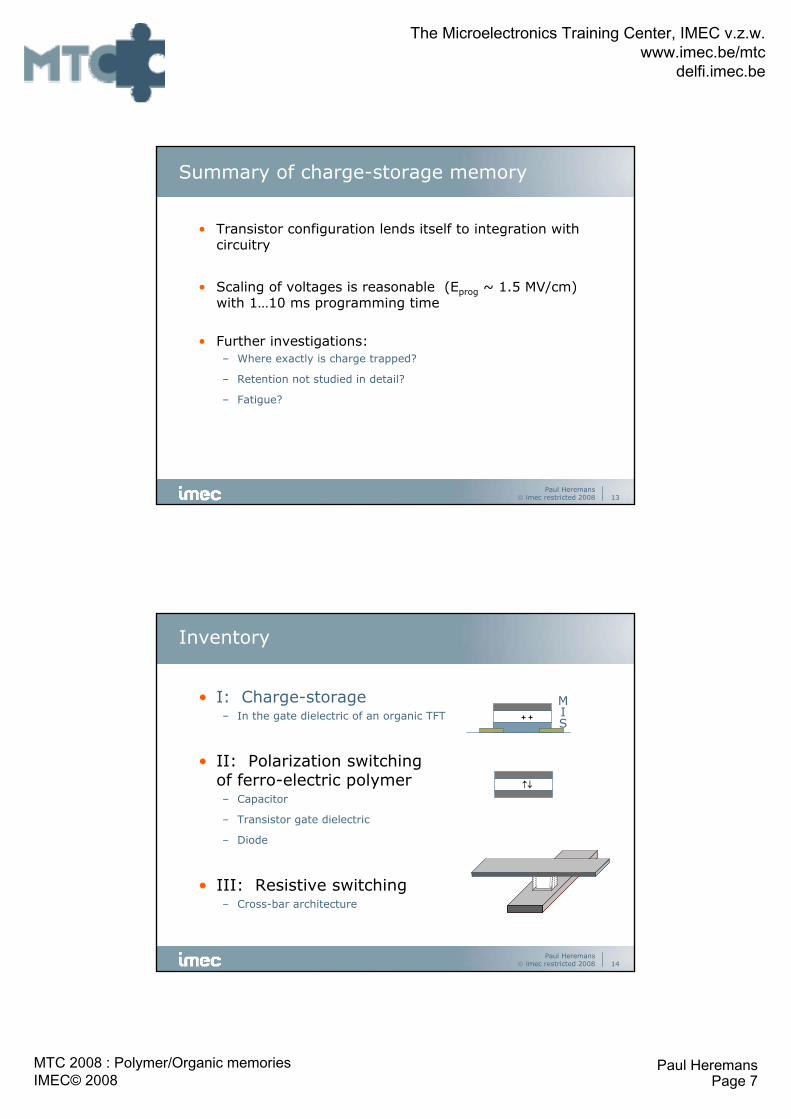
Inventory
• I: Charge-storage– In the gate dielectric of an organic TFT
• II: Polarization switchingof ferro-electric polymer– Capacitor
– Transistor gate dielectric
– Diode
• III: Resistive switching– Cross-bar architecture
++
↑↓
MIS

The Microelectronics Training Center, IMEC v.z.w.www.imec.be/mtc
delfi.imec.be
MTC 2008 : Polymer/Organic memoriesIMEC© 2008
Paul HeremansPage 8
Paul Heremans© imec restricted 2008 15
μeffδ−
δ+δ+
δ−
p(VDF)
H
H F
F
n
CC
H H
F F
=C
C
H H
F F
Type II: Ferro-electric polymer
• poly(vinylidene fluoride) PVDF polymer is ferro-electric in β-phase:– Effective dipole moment (μeff= 7x10-30 Cm) perpendicular to polymer chain
• poly(vinylidene fluoride / trifluoroethylene) P(VDF-TrFE) co-polymer is spontaneously ferro-electric – Due to steric hindrance of F atoms :
SOLVAY
e.g. Katz et al., J. Appl. Phys. 91, 1572 (2002)
Paul Heremans© imec restricted 2008 16
Properties of P(VDF-TrFE)
• Operating temperature
Best VDF content

The Microelectronics Training Center, IMEC v.z.w.www.imec.be/mtc
delfi.imec.be
MTC 2008 : Polymer/Organic memoriesIMEC© 2008
Paul HeremansPage 9
Paul Heremans© imec restricted 2008 17
Polarization switching of P(VDF-TrFE) capa
• Very square loops: large Remanent Polarization (Pr~80 mC/m2)• Relatively large Coercitive Field (Ec~ 0.5 MV/cm)• True (large bandgap) insulator
0 20 40 60 80 100 120 140 160 180 200 220
0
20
40
60
80
100
P r [m
C/m
2 ]
Field [MV/m]
Paul Heremans© imec restricted 2008 18
Polarization switching of P(VDF-TrFE) capa
• Switching time τs depends on applied field E– Consistent with “nucleation and growth”
– 1-10 Micro-second range in reach with E ~ 3-4 Ec (1.5 – 2 MV/cm)
Eswατ exp∝
Naber et al., Appl. Phys. Lett., Vol. 85, No. 11, 2004

The Microelectronics Training Center, IMEC v.z.w.www.imec.be/mtc
delfi.imec.be
MTC 2008 : Polymer/Organic memoriesIMEC© 2008
Paul HeremansPage 10
Paul Heremans© imec restricted 2008 19
Polarization switching of P(VDF-TrFE) capa
• Data retention: excellent stability
0
20
40
60
80
100
0 10 20 30 40 50 60
Time [Hours]
P r [m
C/m
2 ]
Philips
Paul Heremans© imec restricted 2008 20
P(VDF-TrFE) ferro-electric capacitor array
• Passive array• Destructive read-out• External reader• Fully printed on plastic foil
• Application examples:– Game cards
• Player level programmedon card
– Brand protection
Thin-Film ASA http://www.thinfilm.se

The Microelectronics Training Center, IMEC v.z.w.www.imec.be/mtc
delfi.imec.be
MTC 2008 : Polymer/Organic memoriesIMEC© 2008
Paul HeremansPage 11
Paul Heremans© imec restricted 2008 21
Inventory
• I: Charge-storage– In the gate dielectric of an organic TFT
• II: Polarization switchingof ferro-electric polymer– Capacitor
– Transistor gate dielectric
– Diode
• III: Resistive switching– Cross-bar architecture
++
↑↓
MIS
Paul Heremans© imec restricted 2008 22
Ferro-electric organic memory transistors
FIG. 1b. Schematic diagrams of FETs with oriented dipoles embedded in the gate dielectric and influencing the effective voltage at the dielectric-semiconductor interface.
FIG. 3. Hysteretic drain current as a function of gate voltage for polymer FeFETs (Au / P(VDF/TrFE) / MEHPPV). The ferroelectric layer thickness is 0.85 μm. The arrows show the clockwise hysteresis of the drain current consistent with accumulation and depletion of p-type charge carriers. The FeFETs had previously been brought into the off-state.
Naber et al., Nat. Mat. 4, 243 (2005)

The Microelectronics Training Center, IMEC v.z.w.www.imec.be/mtc
delfi.imec.be
MTC 2008 : Polymer/Organic memoriesIMEC© 2008
Paul HeremansPage 12
Paul Heremans© imec restricted 2008 23
Switching with 85 V / 850 nm gate pulses
Ferro-electric organic memory transistors
Naber et al., Nat. Mat. 4, 243 (2005)
Paul Heremans© imec restricted 2008 24
retention fatigue
Ferro-electric organic memory transistors
Naber et al., Nat. Mat. 4, 243 (2005)
Switching with 77.5 V / 850 nm gate voltage sweep

The Microelectronics Training Center, IMEC v.z.w.www.imec.be/mtc
delfi.imec.be
MTC 2008 : Polymer/Organic memoriesIMEC© 2008
Paul HeremansPage 13
Paul Heremans© imec restricted 2008 25
Naber et al., Nat. Mat. 4, 243 (2005)
Ferro-electric organic memory transistors
~ 1E13 q/cm2
Paul Heremans© imec restricted 2008 26
Summary FE capa and TFT
• Scaling of thickness to ~ 60 nm has been done• Scaling of voltages is reasonable:
Ec ~ 0.5 MV/cmEprog ~ 2X … 3X Ec
• Large remanent polarization Pr~80 mC/m2 Large accumulation charge switching in TFT
• Programming time can scale to the range 1…10 μs (for Eprog ~ 3X … 4X Ec)
• Fatigue may be an issue (beyond 1000 cycles)• Operation temperature limited by TCurie ~ 140 ºC• Preliminary data show excellent retention

The Microelectronics Training Center, IMEC v.z.w.www.imec.be/mtc
delfi.imec.be
MTC 2008 : Polymer/Organic memoriesIMEC© 2008
Paul HeremansPage 14
Paul Heremans© imec restricted 2008 27
Inventory
• I: Charge-storage– In the gate dielectric of an organic TFT
• II: Polarization switchingof ferro-electric polymer– Capacitor
– Transistor gate dielectric
– Diode
• III: Resistive switching– Cross-bar architecture
++
↑↓
MIS
Paul Heremans© imec restricted 2008 28
Ferro-electric memory diode
• Context: 1D-1R cell in cross-bar architecture with non-volatile switcheable resistors.
• Diode with switcheable characteristics
0 V 10 V
0 V
10 V
selected cell
Diode
Switcheable resistor
bit l
ine
word line
1D-1R crossbarRequired element

The Microelectronics Training Center, IMEC v.z.w.www.imec.be/mtc
delfi.imec.be
MTC 2008 : Polymer/Organic memoriesIMEC© 2008
Paul HeremansPage 15
Paul Heremans© imec restricted 2008 29
How we can make a Diode using OSC
• Schottky diode between Ohmic and Rectifying contacts
S. Steudel et al., Nat. Mat., Vol 4, p. 597, 2005
Al
Organic semiconductor
Au
substrate
A
C
E
Paul Heremans© imec restricted 2008 30
Polymer Ferro-Electric Diode
K. Asadi et al., Nat. Mat., Vol 7, p. 547, 2008
P3HT
P(VDF-TrFE)

The Microelectronics Training Center, IMEC v.z.w.www.imec.be/mtc
delfi.imec.be
MTC 2008 : Polymer/Organic memoriesIMEC© 2008
Paul HeremansPage 16
Paul Heremans© imec restricted 2008 31
• 140-250 nm thickness
• Ag electrodes• Poled at +20V/-20V• Areas =
0.3×0.3mm2 to 4×4mm2
Polymer Ferro-Electric Diode
K. Asadi et al., Nat. Mat., Vol 7, p. 547, 2008
Paul Heremans© imec restricted 2008 32
Polymer Ferro-Electric Diode
K. Asadi et al., Nat. Mat., Vol 7, p. 547, 2008

The Microelectronics Training Center, IMEC v.z.w.www.imec.be/mtc
delfi.imec.be
MTC 2008 : Polymer/Organic memoriesIMEC© 2008
Paul HeremansPage 17
Paul Heremans© imec restricted 2008 33
Inventory
• Charge-storage– In the gate dielectric of an organic TFT
• Polarization switching– Capacitor
– Transistor gate dielectric
– Diode
• Resistive switching– Cross-bar architecture
++
↑↓
MIS
Paul Heremans© imec restricted 2008 34
Resistive switching
• Cross-bar architecture• Non-volatile• Non-destructive read• Re-writeable• Materials:
– Charge transfer complexes
– Metal-nanoparticles
– Polymers

The Microelectronics Training Center, IMEC v.z.w.www.imec.be/mtc
delfi.imec.be
MTC 2008 : Polymer/Organic memoriesIMEC© 2008
Paul HeremansPage 18
Paul Heremans© imec restricted 2008 35
Materials 1: charge transfer complexes
• Charge-Transfer complexes:• CuTCNQ and AgTCNQ
R.S. Potember et al., Appl. Phys. Lett. 34 (1979) 405Z. Fan et al., IEEE-NANO, (2003) 588-591
• Bengal Rose, Phloxine, …A. Bandyopadhyay et al., Appl. Phys. Lett. 82 (2003) 1215-1217
• PCBM/TTFC.-W. Chu et al., Adv. Mat. 17 (2005) 1440-1443
CC-
N
NN
NCu
+
I
I
Cl
Cl Cl
I
Cl COONa
O
I
ONaO
CuTCNQ
Bengal Rose
+
+
+
-
-
-
Partially neutral: high σ
+
+
+
+
+ +
- -
- -
- -
Ionized: low σ
Originally proposed mechanism:
Paul Heremans© imec restricted 2008 36
Characteristics of M/CuTCNQ/Al cross-bars
• CuTCNQ (Potember 1979)• Metal: Cu, Ag• Polynitrile π-acceptors: TCNQ (+ derivatives), DDQ,
DCNQI, TCNE, …• Bipolar resistive electrical switching (in air)
Measurement setup Typical log|I|-V curve
10-9
10-8
10-7
10-6
10-5
10-4
Cur
rent
(A)
86420-2-4-6
Voltage Memory (V)
1
3 4
6
Start
25
Typical I-V curve
-300
-200
-100
0
100
Cur
rent
(µA
)
86420-2-4-6
Voltage Memory (V)
32
1 6
54
Start

The Microelectronics Training Center, IMEC v.z.w.www.imec.be/mtc
delfi.imec.be
MTC 2008 : Polymer/Organic memoriesIMEC© 2008
Paul HeremansPage 19
Paul Heremans© imec restricted 2008 37
Materials 2: nanoparticles
• Metallic nanoparticles in organic semiconductor:• Organic/metal-nanocluster/organic system
L. Ma et al., Appl. Phys. Lett. 82 (2003) 1419-1421L. Bozano, Adv. Funct. Mat. 15 (2005) 1933
• Polyaniline nanofiber / Au nanoparticleR.J. Tseng et al., Nano Lett. 5, 2005, 1077-1080
Originally proposed mechanism:
+
Paul Heremans© imec restricted 2008 38
Materials 3: polymers
• Polymers:• Polythiophene derivative
H.S. Majumdar et al., Synth. Met. 140 (2004) 203-206
• Alq3, superyellow PPV, OC1C10, polyspirofluoreneM. Cölle et al., Organic Electronics, 7, 305, 2006
• Isolators such as polystyreneM. Cölle et al., Organic Electronics, 7, 305, 2006
•Polymer blends:• P3HT+EC / PEDOT:PSS+LiCF3SO3+EC
J.H.A. Smits et al., Adv. Mat. 17 (2005) 1169-1173
R1
R2
polymers
Al = Electrode 2
Organic semiconductor
Or
polymer
Electrode 1
substrate

The Microelectronics Training Center, IMEC v.z.w.www.imec.be/mtc
delfi.imec.be
MTC 2008 : Polymer/Organic memoriesIMEC© 2008
Paul HeremansPage 20
Paul Heremans© imec restricted 2008 39
Typical curves for Polymers & NP
Typical characteristics for Metal/Polymer/Metal systems
• UNIPOLAR switching: ON and OFF can be achieved with same voltage polarity• Often possible in two directions
L. Bozano, Adv. Funct. Mat. 15 (2005) 1933
Paul Heremans© imec restricted 2008 40
Characteristics
M. Coelle et al., Organic Electronics 7 (2006) 305–312
Al = Electrode 2
Organic semiconductor
Polymer
Electrode 1
substrate

The Microelectronics Training Center, IMEC v.z.w.www.imec.be/mtc
delfi.imec.be
MTC 2008 : Polymer/Organic memoriesIMEC© 2008
Paul HeremansPage 21
Paul Heremans© imec restricted 2008 41
Mechanism
• Filamentary conduction in “on” state• For many of the devices proposed, interfacial
(native) AlOx contains the current switches
M. Coelle et al. / Organic Electronics 7 (2006) 305–312
These devices are kin to Oxide RRAM!Review by Waser and Aono, Nat. Mat. Vol 6, p. 833, 2007
Similar to “Oxide”, also for “Organic” RRAMunipolar and bipolar switching has been shown
oxide
organic
e.g. “polymer” and NPe.g. CuTCNQ
Paul Heremans© imec restricted 2008 42
Similarity with “nanoelectromechanical” switch ?
L. Bozano, Adv. Funct. Mat. 15 (2005) 1933
nature materials VOL 7 DECEMBER 2008
Y. Li, Nature Materials 7 (2008) 966
Electronic two-terminal bistable graphitic memories

The Microelectronics Training Center, IMEC v.z.w.www.imec.be/mtc
delfi.imec.be
MTC 2008 : Polymer/Organic memoriesIMEC© 2008
Paul HeremansPage 22
Paul Heremans© imec restricted 2008 43
Characteristics of M/CuTCNQ/Al cross-bars
• CuTCNQ (Potember 1979)• Metal: Cu, Ag• Polynitrile π-acceptors: TCNQ (+ derivatives), DDQ,
DCNQI, TCNE, …• Bipolar resistive electrical switching (in air)
Measurement setup Typical log|I|-V curve
10-9
10-8
10-7
10-6
10-5
10-4
Cur
rent
(A)
86420-2-4-6
Voltage Memory (V)
1
3 4
6
Start
25
Typical I-V curve
-300
-200
-100
0
100
Cur
rent
(µA
)
86420-2-4-6
Voltage Memory (V)
32
1 6
54
Start
Paul Heremans© imec restricted 2008 44
Characteristics of M/CuTCNQ/Al cross-bars
• Endurance of 104 write/erase cycles
4
68
1µA
2
4
68
10µA
2
4
Cur
rent
1000080006000400020000Cycle number
ON OFF
VM = -1 V
40003000200010000Counts
4
68
1µA
2
4
68
10µA
2
4
Cur
rent
ON OFF
VM = -1 V
Cycles (cross-bar memory):Au\CuTCNQ\Al: 0.04 mm2
Müller et al., Mater. Res. Soc. Symp. Proc., 997 (2007) I01-10
Pulsed measurements (capacitor):Al\CuTCNQ\Al: 0.005625 mm2
Kever et al., Thin Solid Films, 515 (2006) 1893
• Retention time up to 60h• Operational up to about 80°C
Müller et al., Mater. Res. Soc. Symp. Proc., 997 (2007) I01-10

The Microelectronics Training Center, IMEC v.z.w.www.imec.be/mtc
delfi.imec.be
MTC 2008 : Polymer/Organic memoriesIMEC© 2008
Paul HeremansPage 23
Paul Heremans© imec restricted 2008 45
Characteristics of M/CuTCNQ/Al cross-bars
Müller et al., Appl. Phys Lett., 89 (2006) 223501
Cu SiO2 SiC TaN + Ta SiSiN CuTCNQ
10-11
10-10
10-9
10-8
10-7
10-6
Cur
rent
(A)
6420-2-4Voltage Memory (V)
1
2
3
4
OFF → ON ON → OFF
Mushroom like CuTCNQ growth in 250 nm vias
Single crystal CuTCNQ growth in 100 nm vias
Paul Heremans© imec restricted 2008 46
Phase transition (II→I)(If not consequence of CuTCNQ roughness)Heintz et al. (1999)
Bulk phenomena(phase transition?)Potember et al. (1979)
Switching with c-STM tip → bulk effect (?)Matsumoto et al. (1991)
Bulk phenomena
Investigation of switching in CuTCNQ memory
Cu\CuTCNQ\Al: increase of resistance after air exposureHoagland et al. (1993)
Impedance spectroscopy →highly resistive CuTCNQ\Al interfaceKever et al. (2007)
Reproducible switching for ITO\Al (Al2O3)\CuTCNQ\AlOyamada et al. (2003)
Interfacial effect
Impedance & capacitance measurements →CuTCNQ\Al interface effectSato et al. (1990)
Raman signal of TCNQ during OFF→ON switchingKamitsos et al. (1982) Switching with probe
needles or oxide layersHefczyc et al. (2008)
Apparent contradiction? Two different switching mechanisms?
[Cu+(TCNQ-)]n Cu0x + (TCNQ0)x + [Cu+(TCNQ-)]n-x
high impedance
"OFF state"
low impedance
"ON state"
voltage
R. Mueller et al., proceedings of MRS 2008

The Microelectronics Training Center, IMEC v.z.w.www.imec.be/mtc
delfi.imec.be
MTC 2008 : Polymer/Organic memoriesIMEC© 2008
Paul HeremansPage 24
Paul Heremans© imec restricted 2008 47
Role of interface native oxide in CuTCNQ devices
Further proofs:Yb top contact (same procedure)Encapsulated devices (Miplaza, Eindhoven (NL)) with Al : no switching
Billen et al., Appl. Phys. Lett., 91 (2007) 263507
Cu\CuTCNQ\Al crossbar: 0.04 mm2
10-11
10-10
10-9
10-8
10-7
10-6
10-5
10-4
10-3
Cur
rent
(A)
1050-5Voltage Memory (V)
N2 glovebox (prior to air exposure)
12 4
3
10-11
10-10
10-9
10-8
10-7
10-6
10-5
10-4
10-3
Cur
rent
(A)
1050-5Voltage Memory (V)
N2 glovebox (prior to air exposure) Cycle 1 (after air exposure) Cycle 2 (after air exposure) Cycle 3 (after air exposure) Cycle 4 (after air exposure)
1
2
4
3
air
N2
HV
Paul Heremans© imec restricted 2008 48
Role of interface native oxide in CuTCNQ devices
A. Hefczyc et al., Phys. Stat. Solidi A, 205 (2008) 647
Status of device I is independent of device II
Always same status for devices I and II
15 mμ5 mμ
Al AlAuCuTCNQ
15 mμ5 mμ
Au AuAl
CuTCNQ
II
→ Localized switching at the CuTCNQ\Al interface (no bulk effect)
I
I II

The Microelectronics Training Center, IMEC v.z.w.www.imec.be/mtc
delfi.imec.be
MTC 2008 : Polymer/Organic memoriesIMEC© 2008
Paul HeremansPage 25
Paul Heremans© imec restricted 2008 49
Filamentary conduction in CuTCNQ devices
Heat sensitive infrared camera
Billen et al., Appl. Phys. Lett., 91 (2007) 263507
I-t measurement
-220
-200
-180
-160
-140
-120
-100
-80
I (µA
)
0.1 1 10 100t (s)
Al\CuTCNQ\Al crossbar: 0.04 mm2
switched to the ON state
Paul Heremans© imec restricted 2008 50
Comparison with other types of memories
•Programmable Metallization Cell (PMC)Ag-Ge-S, Cu-Ge-S (Cu and Ag cations, Kozicki et al. NVMWS 2005)Bipolar switching, electrochemical reaction
Ag2STerabe et al., RIKEN Rev., 37 (2001) 7
gap
•Sulfide based memoriesAg2S, Cu2S (Ag+ and Cu+ cations)Solid-state ionic conductor (κ: 1-4 S.cm-1 for silver chalcogenides)bipolar switching, electrochemical reaction, metallic filament
Cu2S, NanoBridge® Technology (NEC)Kaeriyama et al., IEEE J Solid-State Circ., 40 (2005) 168
•CuTCNQCu+ cations (Ag+ cations for AgTCNQ)κ: 0.25 S.cm-1 (phase I, Heintz et al., Inorg. Chem., 38 (1999) 144)Similar switching mechanism?

The Microelectronics Training Center, IMEC v.z.w.www.imec.be/mtc
delfi.imec.be
MTC 2008 : Polymer/Organic memoriesIMEC© 2008
Paul HeremansPage 26
Paul Heremans© imec restricted 2008 51
Proposed model for M1/CuTCNQ/SL/M2
OFF state to ON state:
Cu Cu+
e-
(i)
Cu2+Cu+
e-
(ii)TCNQ- TCNQ
e-(iii)
Cu+
Cu-e
Cu, Au,Pt, ...
Al, Yb,Ti, ...
+ -
porous layer or
gap
easy oxidizable
metal
“noble”metal solid ionic conductor
(Cu+TCNQ-)
growth of Cu
filament
Cu+
Cu+
Cu+Cu+
≈ 20 nm → several μm few nm
reductionoxidation
Rfilament (Rfilament Rgap)RON RCuTCNQ RgapROFF = +
Billen et al., Appl. Phys. Lett., 91 (2007) 263507
Paul Heremans© imec restricted 2008 52
Proposed model for M1/CuTCNQ/SL/M2
ON state to OFF state:
Cu Cu+
e-(i)
Cu2+Cu+
e-
(ii)TCNQ- TCNQ
e-
(iii)
Cu+
Cu-e
Cu, Au,Pt, ...
Al, Yb,Ti, ...
-
porous layer or
gap
easy oxidizable
metal
“noble”metal solid ionic conductor
(Cu+TCNQ-)
dissolution of Cu
filament
Cu+
Cu+
Cu+Cu
+
≈ 20 nm → several μm few nm
oxidation
Rfilament (Rfilament Rgap)RON RCuTCNQ= +
+reduction
RgapROFF
Billen et al., Appl. Phys. Lett., 91 (2007) 263507

The Microelectronics Training Center, IMEC v.z.w.www.imec.be/mtc
delfi.imec.be
MTC 2008 : Polymer/Organic memoriesIMEC© 2008
Paul HeremansPage 27
Paul Heremans© imec restricted 2008 53
Recapituation on switching experiments
Bulk phenomena Interfacial effect
Interfacial effect (oxide layer or nanometer-size gap)
Phase transition (II→I)(If not consequence of CuTCNQ roughness)Heintz et al. (1999)
Bulk phenomena(phase transition?)Potember et al. (1979)
Switching with c-STM tip → bulk effect (?)Matsumoto et al. (1991)
Cu\CuTCNQ\Al: increase of resistance after air exposureHoagland et al. (1993)
Impedance spectroscopy →highly resistive CuTCNQ\Al interfaceKever et al. (2007)
Reproducible switching for ITO\Al (Al2O3)\CuTCNQ\AlOyamada et al. (2003)
Impedance & capacitance measurements →CuTCNQ\Al interface effectSato et al. (1990)
Raman signal of TCNQ during OFF→ON switchingKamitsos et al. (1982) Switching with probe
needles or oxide layersHefczyc et al. (2008)
Paul Heremans© imec restricted 2008 54
Generalisation of the model
• Examples:• CuTNAP, AgTNAP (TNAP = 1 1,11,12,12-tetracyano-2,6-napthoquinodimethane )
Potember et al., J. Am. Chem. Soc., 102 (1980) 3659• CuDDQ (DDQ =2,3-dichloro-5,6-dicyano-p-benzoquinone)
Weitz et al., Nano Lett., 6 (2006) 2810
M M+
e-
(i)
Mn+M+
(n-1)e-
(ii)A- A
e-(iii)
M+
M-e
M, Au,Pt, ...
Al, Yb,Ti, ...
+ -growth of
M filament
M+
M +
M +M +
≈ 20 nm → several μm few nm
reductionoxidation
solid ionic conductor(M+A-)
porous layer or
gap
Switchinglayer
SIC
R. Mueller et al., MRS spring meeting 2008

The Microelectronics Training Center, IMEC v.z.w.www.imec.be/mtc
delfi.imec.be
MTC 2008 : Polymer/Organic memoriesIMEC© 2008
Paul HeremansPage 28
Paul Heremans© imec restricted 2008 55
Summary CuTCNQ crossbar
• Model proposed in which conduction is controlled by metal filaments in a “switching layer” (gap, spacer), formed and dissolved by electrochemistry from ions provided through/from Solid Ionic Conductor
• Improved switching layers are being explored (EMMA)
• Fatigue gradually improves (1E4 cycles)• Temperature limited (T < 80ºC)• Retention unknown• Can be scaled to < 100 nm
Paul Heremans© imec restricted 2008 56
Summary
• Capacitor type:– Ferro-electric capa
• Transistor-types:– Charge storage in dual-layer gate dielectric
– Ferro-electric gate dielectric
• Switching diodes:– Mix of semiconducting polymer and ferro-electric insulator between electrodes
• Switching resistors: – Unipolar and bipolar have been shown in literature
– In the case of the charge-transfer complex M-TCNQ (and similar molecules), the bipolar switching mechanism is traced back to metal filaments in gap layer, and the role of the M-TCNQ is a Solid Ionic Conductor
• Types of Reprogrammable Non-volatile “Organic” memories:
The Microelectronics Training Center, IMEC v.z.w.www.imec.be/mtc
delfi.imec.be
MTC 2008 : Polymer/Organic memoriesIMEC© 2008
Paul HeremansPage 29
Paul Heremans© imec restricted 2008 57
Summary
• Plastic electronic circuits will require one or several forms of electrically reprogrammable non-volatile memory
• For integration in CMOS:– The CuTCNQ cross-bar has been shown to scale to the dimensions of via holes
– The temperature stability of the organic compounds is an issue
• Use of these memories:
• Excellent progress has been done in the understanding of the physics and switching mechanisms, which will allow to further optimize the characteristics
Paul Heremans© imec restricted 2008 58
Acknowledgements
• IMEC research teams– Robert Mueller, Jan Genoe, Maarten Debucquoy, Joris Billen,…
– Dirk Wouters, Ludovic Goux,
• IMEC research partners– Philips, TNO (Gerwin Gelinck, Paul Blom), RWTH, IM2NP, IUNET,
NUMONYX, MDM
• Financial support– Nosce Memorias, FP6 project
– EMMA, FP7 project

The Microelectronics Training Center, IMEC v.z.w.www.imec.be/mtc
delfi.imec.be
MTC 2008 : Polymer/Organic memoriesIMEC© 2008
Paul HeremansPage 30
Paul Heremans© imec restricted 2008 59