organic ferroelectric diodes - tu/e · organic ferroelectric diodes khikhlovskyi, v. published:...
TRANSCRIPT

Organic ferroelectric diodes
Khikhlovskyi, V.
Published: 01/01/2015
Document VersionPublisher’s PDF, also known as Version of Record (includes final page, issue and volume numbers)
Please check the document version of this publication:
• A submitted manuscript is the author's version of the article upon submission and before peer-review. There can be important differencesbetween the submitted version and the official published version of record. People interested in the research are advised to contact theauthor for the final version of the publication, or visit the DOI to the publisher's website.• The final author version and the galley proof are versions of the publication after peer review.• The final published version features the final layout of the paper including the volume, issue and page numbers.
Link to publication
Citation for published version (APA):Khikhlovskyi, V. (2015). Organic ferroelectric diodes Eindhoven: Technische Universiteit Eindhoven
General rightsCopyright and moral rights for the publications made accessible in the public portal are retained by the authors and/or other copyright ownersand it is a condition of accessing publications that users recognise and abide by the legal requirements associated with these rights.
• Users may download and print one copy of any publication from the public portal for the purpose of private study or research. • You may not further distribute the material or use it for any profit-making activity or commercial gain • You may freely distribute the URL identifying the publication in the public portal ?
Take down policyIf you believe that this document breaches copyright please contact us providing details, and we will remove access to the work immediatelyand investigate your claim.
Download date: 08. Jun. 2018
Organic Ferroelectric Diodes
PROEFSCHRIFT
ter verkrijging van de graad van doctor aan de Technische Universiteit Eindhoven, op gezag van de
rector magnificus prof.dr.ir. F.P.T. Baaijens, voor een commissie aangewezen door het College voor
Promoties, in het openbaar te verdedigen op woensdag 4 november 2015 om 16:00 uur
door
Vsevolod Khikhlovskyi
geboren te Zhovti Vody, Oekraine

Dit proefschrift is goedgekeurd door de promotoren en de samenstelling van de promotiecommissie is als volgt:
voorzitter: prof.dr.ir. G.M.W. Kroesen 1
e promotor: prof.dr.ir. M. Kemerink (Universiteit
van Linköping) 2
e promotor: prof.dr. G.H. Gelinck
copromotor(en): prof.dr.ir. R.A.J. Janssen leden: prof.dr. B. Noheda (RUG)
prof.dr. D.M. de Leeuw (MPIP Mainz) prof.dr. P.M. Koenraad
Het onderzoek of ontwerp dat in dit proefschrift/proefontwerp wordt beschreven is uitgevoerd in overeenstemming met de TU/e Gedragscode Wetenschapsbeoefening.


A catalogue record is available from the Eindhoven University of Technology Library
ISBN: 978-90-386-3943-7
1
Contents
Chapter 1
Introduction 5
1.1 Introduction 6
1.2 Ferroelectric polymer memories 8
1.3 Characterization of the ferroelectric polarization 14
1.3.1 Piezoresponce force microscopy 14
1.3.2 Double-wave method 15
1.4 Outline of the thesis 17
1.5 References 18
Chapter 2
Multi-bit organic ferroelectric memory 23
2.1 Introduction 24
2.2 Results and discussion 24
2.2.1 Study of ferroelectric properties of P(VDF-TrFE) 24
2.2.2 Dipole switching theory (DST) 26
2.2.3 Multi-bit in P(VDF-TrFE) based capacitor 30
2.3 Conclusions 32
2.4 Experimental 33
2.5 References 33

Contents
2
Chapter 3
Nanoscale ferroelectric diodes 35
3.1 Introduction 36
3.2 Results and discussion 37
3.2.1 Morphology and ferroelectric properties of the blend at the local
scale
37
3.2.2 Electrical properties of the device at the local scale 38
3.2.3 Modeling of the electrical properties of the device at the local scale 42
3.2.4 Single domain poling 45
3.3 Conclusions 46
3.4 Experimental 46
3.5 References 47
Chapter 4
3D-morphology reconstruction of nanoscale phase-separation in polymer memory
blends 51
4.1 Introduction 52
4.2 Results and discussion 53
4.2.1 Selective dissolution approach 53
4.2.2 Statistical analysis of the blend morphology 57
4.3 Conclusions 60
4.4 Experimental 61
4.5 References 61
Chapter 5
Surface directed phase separation of semiconductor ferroelectric polymer blends
and their use in non-volatile memories 65
5.1 Introduction 66
5.2 Results and discussion 67
5.2.1 Blend layer processing on non-patterned substrates 67
5.2.2 Blend layer processing on substrates with patterned SAMs 71
5.2.3 Simulations 74
5.2.4 Electrical characterization of polymer blend films in memory
switches
76
5.3 Conclusions 78
5.4 Experimental 78
5.5 References 81

Contents
3
Chapter 6
Detailed study of the wetting layer and its influence on the performance of the
ferroelectric diode
85
6.1 Introduction 86
6.2 Results and discussion 86
6.2.1 Detailed study of the wetting layer 86
6.3 Conclusions 92
6.4 Experimental 92
6.5 References 93
Chapter 7
Data retention in ferroelectric diodes 95
7.1 Introduction 96
7.2 Results and discussion 97
7.2.1 Electrical and memory characteristics of a ferroelectric diode 97
7.2.2 Underlying mechanism of the information loss 98
7.2.3 Studying and improving the data retention 102
7.3 Conclusions 105
7.4 Experimental 106
7.5 References 106
Appendix A
109
Appendix B
111
Summary
115
Sumenvatting
119
Curriculum vitae
123
List of publications
125
Acknowledgements
127

4

5
Chapter 1
Introduction
Chapter 1: Introduction
6
1.1 Introduction
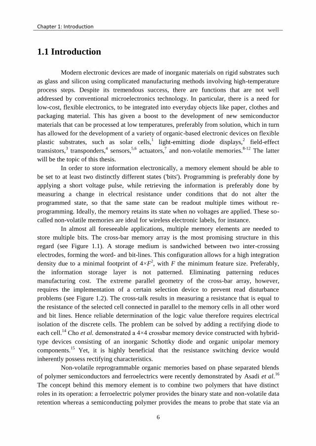
Modern electronic devices are made of inorganic materials on rigid substrates such
as glass and silicon using complicated manufacturing methods involving high-temperature
process steps. Despite its tremendous success, there are functions that are not well
addressed by conventional microelectronics technology. In particular, there is a need for
low-cost, flexible electronics, to be integrated into everyday objects like paper, clothes and
packaging material. This has given a boost to the development of new semiconductor
materials that can be processed at low temperatures, preferably from solution, which in turn
has allowed for the development of a variety of organic-based electronic devices on flexible
plastic substrates, such as solar cells,1 light-emitting diode displays,
2 field-effect
transistors,3 transponders,
4 sensors,
5,6 actuators,
7 and non-volatile memories.
8-12 The latter
will be the topic of this thesis.
In order to store information electronically, a memory element should be able to
be set to at least two distinctly different states ('bits'). Programming is preferably done by
applying a short voltage pulse, while retrieving the information is preferably done by
measuring a change in electrical resistance under conditions that do not alter the
programmed state, so that the same state can be readout multiple times without re-
programming. Ideally, the memory retains its state when no voltages are applied. These so-
called non-volatile memories are ideal for wireless electronic labels, for instance.
In almost all foreseeable applications, multiple memory elements are needed to
store multiple bits. The cross-bar memory array is the most promising structure in this
regard (see Figure 1.1). A storage medium is sandwiched between two inter-crossing
electrodes, forming the word- and bit-lines. This configuration allows for a high integration
density due to a minimal footprint of 4×F2, with F the minimum feature size. Preferably,
the information storage layer is not patterned. Eliminating patterning reduces
manufacturing cost. The extreme parallel geometry of the cross-bar array, however,
requires the implementation of a certain selection device to prevent read disturbance
problems (see Figure 1.2). The cross-talk results in measuring a resistance that is equal to
the resistance of the selected cell connected in parallel to the memory cells in all other word
and bit lines. Hence reliable determination of the logic value therefore requires electrical
isolation of the discrete cells. The problem can be solved by adding a rectifying diode to
each cell.14
Cho et al. demonstrated a 4×4 crossbar memory device constructed with hybrid-
type devices consisting of an inorganic Schottky diode and organic unipolar memory
components.15
Yet, it is highly beneficial that the resistance switching device would
inherently possess rectifying characteristics.
Non-volatile reprogrammable organic memories based on phase separated blends
of polymer semiconductors and ferroelectrics were recently demonstrated by Asadi et al.16
The concept behind this memory element is to combine two polymers that have distinct
roles in its operation: a ferroelectric polymer provides the binary state and non-volatile data
retention whereas a semiconducting polymer provides the means to probe that state via an
Introduction
7
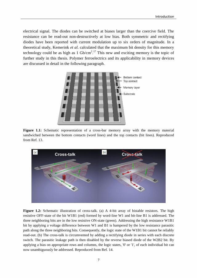
electrical signal. The diodes can be switched at biases larger than the coercive field. The
resistance can be read-out non-destructively at low bias. Both symmetric and rectifying
diodes have been reported with current modulation up to six orders of magnitude. In a
theoretical study, Kemerink et al. calculated that the maximum bit density for this memory
technology could be as high as 1 Gb/cm2.17
This new and exciting memory is the topic of
further study in this thesis. Polymer ferroelectrics and its applicability in memory devices
are discussed in detail in the following paragraph.
Figure 1.1: Schematic representation of a cross-bar memory array with the memory material
sandwiched between the bottom contacts (word lines) and the top contacts (bit lines). Reproduced
from Ref. 13.
Figure 1.2: Schematic illustration of cross-talk. (a) A 4-bit array of bistable resistors. The high
resistive OFF-state of the bit W1B1 (red) formed by word-line W1 and bit-line B1 is addressed. The
three neighboring bits are in the low resistive ON-state (green). Addressing the high resistance W1B1
bit by applying a voltage difference between W1 and B1 is hampered by the low resistance parasitic
path along the three neighboring bits. Consequently, the logic state of the W1B1 bit cannot be reliably
read-out. (b) The cross-talk is circumvented by adding a rectifying diode in series with each discrete
switch. The parasitic leakage path is then disabled by the reverse biased diode of the W2B2 bit. By
applying a bias on appropriate rows and columns, the logic states, '0' or '1', of each individual bit can
now unambiguously be addressed. Reproduced from Ref. 14.

Chapter 1: Introduction
8
1.2 Ferroelectric polymer memories
In general, ferroelectricity is described as a property of a material that possesses
spontaneous electric polarization, the direction of which can be reversed by an external
electric field. Experimentally, the reversal of the spontaneous polarization is observed as a
single ferroelectric hysteresis loop shown in Figure 1.3. It contains important characteristics
of the ferroelectric material: remnant polarization (Pr) – the ferroelectric polarization at
zero electric field – and the coercive voltage (Vc) – the minimal electric voltage required to
reverse the direction of the polarization.
One of the most promising, most studied and most commonly used organic
ferroelectric materials is P(VDF-TrFE) ‒ a random copolymer of vinylidene fluorine (VDF,
-CH2-CF2-) and trifluoroethylene (TrFE, -CFH-CF2-), schematically shown in Figure 1.4a.
Its ferroelectric properties originate from the difference in electronegativity between
fluorine, carbon and hydrogen yielding a large net dipole perpendicular to the polymer
chain direction. P(VDF-TrFE) has several advantageous properties including a large
remnant polarization, excellent polarization stability, low leakage for high resistivity and
switching times as short as 1 microsecond. Furthermore, it is intrinsically bistable, i.e. it
does not require a voltage to keep its polarization state. It can be processed from solution at
low temperatures, opening the possibility of using a wide range of plastic substrates instead
of glass – saving weight and making the final product thinner and virtually unbreakable. It
is therefore ideally suited for next-generation organic electronics applications that require
re-programmable, non-volatile memories. Owing to its piezoelectric and pyroelectric
properties this material is used in other applications as well, such as transducers,18
sensors,19
and actuators.20,21
Figure 1.3: Schematic representation of a ferroelectric hysteresis loop. Pr and Vc indicate remnant
polarization and coercive voltage, respectively.

Ferroelectric polymer memories
9
Figure 1.4: Schematic representation of the chemical structures of (a) ferroelectric polymer P(VDF-
TrFE) and (b) semiconducting polymer F8BT.
Different types of P(VDF-TrFE)-based memories have been reported:
capacitors,22,23
thin-film transistors12
and ferroelectric diodes.16
The basic layout of each of
these device types is shown in Figure 1.5.
Figure 1.5: Schematic representation of (a) ferroelectric capacitor; (b) ferroelectric thin-film
transistor; (c) ferroelectric diode. Ferroelectric and semiconductor are denoted as FE and SC
respectively.
In the ferroelectric capacitor the ferroelectric film is sandwiched between two
metal electrodes (see Figure 1.5a). The ferroelectric can be polarized by applying a
sufficiently large electric field across the electrodes. Depending on the direction of the
polarization, the memory is in its '1' state or in its '0' state. One important advantage of the
ferroelectric capacitor is the possibility to integrate them in the form of cross-bar arrays,
without the need for transistors or other electronic components. Another advantage is that
the information is non-volatile, i.e. the ferroelectric polarization remains when the power is
turned off. In a typical memory array, the capacitors are defined by patterning the top
electrode into columns and the bottom electrodes into rows. The memory state from a

Chapter 1: Introduction
10
capacitor is changed by addressing the corresponding row and column and applying a bias
that will provide the desired ferroelectric polarization. To program all memory elements,
each row is sequentially addressed. To read out the polarization state of each memory
element, again a sufficiently large voltage is applied and external electronics is used to
detect switching charge. The expected switching charge is 2×Pr, but only when the
ferroelectric polarization is reversed. This gives two problems. Firstly, downscaling of the
memory areas implies detecting less switching charge, and requires more sensitive
(expensive) readout electronics outside the array. Second, as read-out of the state occurs via
the detection of the switching current by applying a voltage that exceeds the coercive
voltage, the original state may be changed. This is the problem of so-called destructive
read-out. It is possible to set back the memory to its original state, but this requires an extra
step.
In a ferroelectric thin-film transistor the ferroelectric is used as a gate dielectric in
an otherwise conventional field effect transistor (see Figure 1.5b).12
The polarization of the
ferroelectric layer alters the threshold voltage of the field effect transistor thus producing
distinctly different conductivity states at a given potential depending upon the polarization.
Only a small source-drain potential is required to read out the state. The ferroelectric thin-
film transistor thus allows the polarization state to be read without altering the polarization.
This provides the advantage that the memory transistor is not subjected to the destructive
read/rewrite cycle commonly employed in ferroelectric capacitors. A cost for this
improvement is the increased complexity of the device and the associated increase in the
number of layers.
The ferroelectric diode was first demonstrated by Asadi et al.16,24-27
A spin-coated
film that is sandwiched between two metal electrodes consists of pillars of a
semiconducting polymer, continuous from top to bottom, embedded in a ferroelectric
matrix. A schematic presentation of the cross-section of a diode based on the blend is given
in Figure 1.5c. Because of the insulating ferroelectric matrix transport of the majority of
charge carriers is possible only via the semiconducting phase. Work function(s) of the
metal contact(s) are purposely chosen to yield substantial injection barrier(s) into the
semiconductor. Without ferroelectric polarization, charge injection is therefore limited and
the current in the device is low. When the ferroelectric is poled in the right direction the
polarization field of the ferroelectric apparently lowers the injection barrier at the
semiconductor-metal interface as a higher device current is observed.16
When the
ferroelectric is poled in the other direction, the current is low again. A bistable resistive
switch is thus obtained. It has to be noted that the diodes can be switched at biases larger
than the coercive field. Originally, the switching mechanism of the device was proposed to
be related to a particular morphology in which ferroelectric polarization charges induce
counter charges in the semiconductor, facilitating injection.16
Later, it was proposed on
basis of numerical calculations that the stray field of the ferroelectric might be the driving
force for resistive switching of the ferroelectric diode.17
However, at that moment no
experimental evidence was presented to confirm this theoretical model.

Ferroelectric polymer memories
11
Figure 1.6b shows the corresponding working principle of the device that is
programmed in the ON-state in the case of two injection-limiting (non-Ohmic) contacts. In
the scenario of Ref. 17, the stray field from the ferroelectric, shown with black dotted
arrows, enhances injection of charge carriers into the semiconductor. If the stray field is
sufficiently large, it can lower the injection barrier and locally make the contact Ohmic.
The current then becomes space charge limited, i.e. bulk limited.24
When the device is
programmed in the OFF-state the stray field actually increases the injection barrier, further
suppressing the current in the device (see Figure 1.6c). Figures 1.6a-c also provide the
energy diagram of the device in the corresponding three distinct cases. Black, red and blue
curves in Figure 1.6a-c correspond to the device with a ferroelectric which is non-poled,
poled upwards and downwards respectively. It is clear that only the upwards direction of
the polarization lowers the injection barrier, but does so for both types of charge carriers.
Finally, I-V characteristics of P(VDF-TrFE):F8BT (poly[(9,9–di–n–octylfluorenyl-2,7–
diyl)–alt‒(benzo[2,1,3]thiadiazol-4,8-diyl)], see Figure 1.4b) active blend sandwiched
between gold electrodes are shown in Figure 1.7. Starting from the OFF-state, i.e. with
downward polarization (see Figure 1.6c), the device turns on once the coercive voltage of
the ferroelectric is exceeded. On the downward sweep the device remains in the ON-state
due to the upward polarization, resulting in a hysteretic loop.14
Hence the resistance can be
read-out non-destructively at low bias. Both symmetric and rectifying diodes have been
reported with current modulation up to six orders of magnitude. By deliberately varying the
HOMO energy of the semiconductor and the work-function of the metal electrode, it is
demonstrated that injection barriers up to (nominally) 1.6 eV can be surmounted by the
ferroelectric polarization.24
Such device promises the best characteristics of both types of the devices
mentioned above – ferroelectric bistability, non-destructive resistive readout and current
rectification. It is important to mention that the device satisfies the rectification requirement
mentioned above. By sandwiching this polymer blend film between rows and columns of
metal electrode lines, where each intersection makes up one memory cell, 1 kilobit cross-
bar arrays with bit densities up to 10 kb/cm2 have been demonstrated by van Breemen et
al.28
So far most of the experimental reports focused on the macroscopic electrical
characteristics of such devices16,28,29
and the mechanism of device operation is not yet fully
resolved. It has been shown that the operation of ferroelectric diodes strongly depends on
the 3D-morphology of the phase-separated blend.30,31
The combination of detailed
investigation of microstructure and charge transport measurements will lead to
understanding of the switching mechanism including estimations for the injection barriers
that can be tolerated, and the current rectification that can be achieved.

Chapter 1: Introduction
12
Figure 1.6: Schematic representation of the structure, the operation mechanism and the energy
diagram of ferroelectric diode. (a) Simplified view of the cross-section and energy diagram of the
ferroelectric diode. Green and blue regions correspond to the ferroelectric and semiconducting
polymers, respectively. Top and bottom metal electrodes (possibly different materials) are indicated
in grey. (b) Device in the ON-state. (c) Device in the OFF-state. The stray field increases the injection
barrier, suppressing the current in the device. Minuses (‒) and pluses (+) indicate polarization charges
in the ferroelectric. Black dashed arrows indicate the stray field from the ferroelectric. The stray field
lowers the injection barrier leading to nearly Ohmic contact(s) and space charge limited current
(SCLC).
Experimental
13
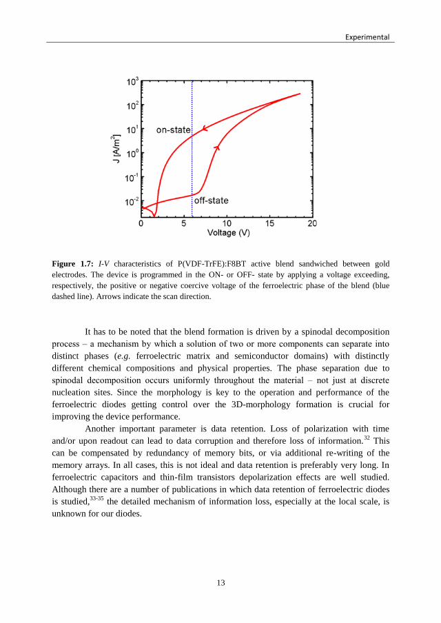
Figure 1.7: I-V characteristics of P(VDF-TrFE):F8BT active blend sandwiched between gold
electrodes. The device is programmed in the ON- or OFF- state by applying a voltage exceeding,
respectively, the positive or negative coercive voltage of the ferroelectric phase of the blend (blue
dashed line). Arrows indicate the scan direction.
It has to be noted that the blend formation is driven by a spinodal decomposition
process ‒ a mechanism by which a solution of two or more components can separate into
distinct phases (e.g. ferroelectric matrix and semiconductor domains) with distinctly
different chemical compositions and physical properties. The phase separation due to
spinodal decomposition occurs uniformly throughout the material ‒ not just at discrete
nucleation sites. Since the morphology is key to the operation and performance of the
ferroelectric diodes getting control over the 3D-morphology formation is crucial for
improving the device performance.
Another important parameter is data retention. Loss of polarization with time
and/or upon readout can lead to data corruption and therefore loss of information.32
This
can be compensated by redundancy of memory bits, or via additional re-writing of the
memory arrays. In all cases, this is not ideal and data retention is preferably very long. In
ferroelectric capacitors and thin-film transistors depolarization effects are well studied.
Although there are a number of publications in which data retention of ferroelectric diodes
is studied,33-35
the detailed mechanism of information loss, especially at the local scale, is
unknown for our diodes.

Chapter 1: Introduction
14
1.3 Characterization of the ferroelectric polarization
Ferroelectric polarization in a ferroelectric capacitor is typically studied in a so-
called Sawyer-Tower setup. The switching charge due to changes in ferroelectric
polarization is detected and separated from other (leakage) currents by applying a so-called
PUND (positive up negative down) scheme.36,37
This technique can however not be applied
in our ferroelectric diodes, due to their macroscopic conductivity that overwhelms the
ferroelectric switching currents. Therefore, several new methods needed to be employed to
unravel the operational mechanism of the ferroelectric diode. In particular, the double-wave
method (DWM) and piezoresponce force microscopy (PFM) were used at respectively the
macroscopic and microscopic levels. Scanning probe techniques were used to measure the
voltage and current spatially resolved with the aim to experimentally investigate scaling of
the current transport with the domain size.
1.3.1 Piezoresponce force microscopy
In 1992, Guthner and Dransfeld first reported piezoresponse force microscopy
(PFM).36
PFM is a tool for local imaging, spectroscopy and manipulation of piezoelectric
and ferroelectric materials. PFM relies on the inverse piezoelectric effect, i.e. a local
mechanical deformation in response on an electrical stimulation. The deformation of a
material in the direction perpendicular to the film surface ‒ ∆S is linked to the applied
electric field ‒ E via a so-called effective piezoelectric coefficient or piezoelectric modulus
‒ d33 by ∆S = d33×E.38
It has to be noted that in case of P(VDF-TrFE) d33 is negative.39
Typical PFM uses a standard scanning force microscope (SFM) that operates in contact
mode. An oscillating voltage is applied to the conductive tip of the SFM. Because of the
piezoelectric effect the voltage-induced deformation of the sample leads to periodic
Figure 1.8: Schematic representation of vertical PFM on ferroelectric diode, sketched in the same
color coding as Figure 1.6. The effective piezoelectric coefficient ‒ d33 > 0.

Double-wave method
15
vibrations of the sample surface which are transmitted to the tip. The resulting oscillations
of the cantilever are detected as the first harmonic component of the tip deflection and can
be read out with the help of a lock-in amplifier. Figure 1.8 shows a schematic
representation of vertical PFM on ferroelectric diode. It is clear that the PFM signal comes
only from the ferroelectric part of the blend. In Chapter 3, PFM, in combination with other
scanning probe microscopy (SPM) techniques, is used to reveal the working mechanism of
the ferroelectric diode at the local scale.
1.3.2 Double-wave method
Clearly there is a strong demand for accurate measurements of the key properties
of the ferroelectric in actual devices ‒ coercive voltage and remnant polarization. A proper
and conceptually simple way of doing that is the double-wave method (DWM), which is a
powerful tool for accurately measuring ferroelectric hysteresis loops.40,41
The concept of the
DWM is based on the idea that the polarization state of a ferroelectric can be probed by
flipping its polarization and detecting the corresponding switching charges.
The DWM was realized by using the experimental setup shown in Figure 1.9. It
consists of a signal generator (SG, typically a function generator connected to a voltage
amplifier), a picoammeter (A), an oscilloscope (OSC) and the device. The signal generator,
the picoammeter and the device are connected in series whereas an oscilloscope (OSC) is
connected in parallel with the analog output of the picoammeter (VOUT). Thus the signal
generator is used for constructing an appropriate input signal applied to the device. At the
same time the switching charges of the device and the applied voltage can be measured and
visualized by the oscilloscope.
Figure 1.9: Schematic representation of the experimental setup used to study the ferroelectric
properties of the devices. A signal generator (SG), a picoammeter (A), an oscilloscope (OSC) and the
device are assembled together.

Chapter 1: Introduction
16
Figure 1.10 shows a typical input signal used in the DWM-based experiments for
measuring inner and saturated ferroelectric hysteresis loops together with the corresponding
schematic current responses. The preparation part of the signal is used for constructing the
desired polarization state of the ferroelectric. The probing part is used for studying the
prepared ferroelectric polarization. To probe the ferroelectric polarization a triangular
pulse, labeled '1' in Figure 1.10, is applied and the corresponding switching current is read
out. Contributions from displacement and the leakage currents can be determined with a
second probing pulse – '2' in Figure 1.10. As this pulse is equal in size and slope to the first,
no polarization switching occurs, whereas displacement and leakage currents are, in lowest
order, the same. Red solid curves, labeled '1' and '2' in Figure 1.10, represent the
corresponding schematic current responses. The shaded area corresponds to the current
associated with the switching of the ferroelectric polarization. Dotted and dashed black
lines represent current responses due to the leakage and the displacement contribution,
respectively. Thus using the response to the second pulse all unwanted responses can be
subtracted from the response to the first pulse, giving solely the voltage-dependent
switching response of the ferroelectric. Moreover the displacement current can upfront be
Figure 1.10: Schematic representation of the signals used in the DWM for measuring inner and
saturated ferroelectric hysteresis loops and corresponding schematic current responses. The amplitude
Vmax of the preparation signal is chosen to be well above the coercive voltage of the ferroelectric
capacitor. Different probing signals Vi have the same ramping speeds but different amplitudes for
measuring inner ferroelectric hysteresis loops. Red solid curves represent schematic current responses
measured with the probing signals '1' and '2'. The shaded area corresponds to the switching current
associated with the reversal of the ferroelectric polarization. Dotted and dashed black lines represent
currents due to leakage and displacement, respectively.

Outline of the thesis
17
significantly suppressed by doing slow measurements – the so-called quasi-static regime of
the DWM. In addition the preparation part of the signal can be changed as well as the
probing one (Vi in Figure 1.10), giving the possibility to study different switching
properties of a ferroelectric material. Hence the DWM provides a simple and a powerful
tool for detailed study of ferroelectrics. In Chapter 2 and 7 the DWM was used to
manipulate and measure the polarization state of the P(VDF-TrFE)-based capacitors and
diodes.
It should be noted that the DWM originates from the so-called PUND (positive
'up' negative 'down') approach.36,37
The basic idea behind both methods is similar and can
be summarized as flipping the polarization state of the ferroelectric and detecting both the
switching (i.e. associated with the ferroelectric polarization) and the nonswitching currents
(i.e. displacement and leakage current). However, the PUND approach is usually associated
with step-like voltage pulses. It often serves for transient-type measurements or for
determining a total polarization of the ferroelectric material. At the same time the DWM
uses continuous transients, for instance linearly increasing/decreasing voltages, giving rise
to much lower displacement currents. Hence it is more suitable for the quasi-static regime
in which we are interested here.
1.4 Outline of the thesis
The aim of the research described in this thesis is focused on the development,
characterization and optimization of ferroelectric P(VDF-TrFE)-based memory devices.
In Chapter 2, a multi-bit organic ferroelectric-based non-volatile memory with
binary readout from a simple capacitor structure is introduced. The working principle of the
multi-bit device is quite general and only demands fulfillment of three requirements
described in Chapter 2. We showed experimentally that the organic ferroelectric polymer ‒
P(VDF-TrFE) - qualifies for being a multi-bit storage medium. Hence we demonstrated a 3-
bit data P(VDF-TrFE)-based storage element. In addition, we measured the ferroelectric
properties (Vc and Pr) of P(VDF-TrFE) that will be used in the rest of the thesis.
In Chapter 3, the operational mechanism of the ferroelectric diode based on the
blend of P(VDF-TrFE):F8BT is studied at the nanoscale. Various scanning probe
techniques were combined with numerical modeling. Resistive switching is shown to result
from modulation of the charge injection barrier at the semiconductor‒electrode interfaces.
It has been proven experimentally that the modulation is driven by the stray field of the
polarization charges in the ferroelectric phase and consequently is restricted to regions
where semiconductor and ferroelectric phases exist in close vicinity.
In Chapter 4, we study the 3D nanoscale morphology of P(VDF-TrFE):F8BT by
AFM and statistical analysis, by selectively dissolving the ferroelectric and semiconductor
components in the blend. We found that the blend consists of a ferroelectric matrix with

Chapter 1: Introduction
18
three types of embedded semiconductor domains. In addition, the existence of a thin
wetting layer at the bottom electrode was revealed. The criteria for the general applicability
of the presented technique are discussed as well. Thus a simple approach for studying the
morphology of the blend at the local scale was introduced.
In Chapter 5, the polymer phase separation of P(VDF-TrFE):F8BT blends is
studied in detail. It was also demonstrated that it is possible to direct the semiconducting
domains of a phase-separating mixture of P(VDF-TrFE) and F8BT in a thin film into a
highly ordered 2D lattice by means of surface directed phase separation. By optimizing the
ratio of the blend components, the number of electrically active semiconductor domains is
maximized. Thus the electrical performance of the memories was improved.
In Chapter 6, the device structure and its impact on the device performance are
studied by advanced scanning probe techniques. We found that a thin wetting layer
drastically influences the device performance by hindering the ferroelectric polarization in
one of the bias directions. An optimal and simple fabrication recipe to avoid the formation
of this wetting layer is found. The new fabrication provides an improved blend structure
that offers better device performance.
In Chapter 7, the data retention of the ferroelectric diodes is studied. It was found
that the data retention is intimately linked to the morphology of the phase-separated
polymer blend and, surprisingly, is due to polarization loss in a narrow region around the
semiconducting domains. We argue that the depolarization is driven by an energy
minimization process and inherently present in this type of phase-separated polymer blends.
In Chapter 8, a summary and an outlook are presented.
1.5 References
[1] D. Gebeyehu, C.J. Brabec, F. Padinger, T. Fromherz, J.C. Hummelen, D. Badt, H.
Schindler, N.S. Sariciftci, The interplay of efficiency and morphology in photovoltaic
devices based on interpenetrating networks of conjugated polymers with fullerenes, Synth.
Met. 2001, 118, 1.
[2] L. Zhou, A. Wanga, S.-C. Wu, J. Sun, S. Park, T.N. Jackson, All-organic active matrix
flexible display, Appl. Phys. Lett. 2006, 88, 083502.
[3] G.H. Gelinck, H.E.A. Huitema, E. van Veenendaal, E. Cantatore, L. Schrijnemakers,
J.B.P.H. van der Putten, T.C.T. Geuns, M. Beenhakkers, J.B. Giesbers, B.-H. Huisman, E.J.
Meijer, E.M. Benito, F.J. Touwslager, A.W. Marsman, B.J.E. van Rens, D.M. de Leeuw,
Flexible active-matrix displays and shift registers based on solution-processed organic
transistors, Nat. Mater. 2004, 3, 106.
[4] P.F. Baude, D.A. Ender, M.A. Haase, T.W. Kelley, D.V. Muyres, S.D. Theiss, Pentacene-
based radio-frequency identification circuitry, Appl. Phys. Lett. 2003, 82, 3964.
[5] T. Someya, Y. Kato, T. Sekitani, S. Iba, Y. Noguchi, Y. Murase, H. Kawaguchi, T. Sakurai,
Conformable, flexible, large-area networks of pressure and thermal sensors with organic
transistor active matrixes, Proc. Natl. Acad. Sci. U.S.A. 2005, 102, 12321.

References
19
[6] T. Sekitani, T. Yokota, U. Zschieschang, H. Klauk, S. Bauer, K. Takeuchi, M. Takamiya, T.
Sakurai, T. Someya, Organic nonvolatile memory transistors for flexible sensor arrays,
Science 2009, 326, 1516.
[7] T. Sekitani, M. Takamiya, Y. Noguchi, S. Nakano, Y. Kato, T. Sakurai, T. Someya, A
large-area wireless power-transmission sheet using printed organic transistors and plastic
MEMS switches, Nat. Mater. 2007, 6, 413.
[8] C.A. Nguyen, S.G. Mhaisalkar, J. Ma, P.S. Lee, Enhanced organic ferroelectric field effect
transistor characteristics with strained poly(vinylidene fluoride-trifluoroethylene) dielectric,
Org. Electron. 2008, 9, 1087.
[9] K.H. Lee, G. Lee, K. Lee, M.S. Oh, S. Im, Flexible low voltage nonvolatile memory
transistors with pentacene channel and ferroelectric polymer, Appl. Phys. Lett. 2009, 94,
093304.
[10] T. Sekitani, K. Zaitsu, Y. Noguchi, K. Ishibe, M. Takamiya, T. Sakurai, T. Someya, Printed
nonvolatile memory for a sheet-type communication system, IEEE Trans. Electron. Dev.
2009, 56, 1027.
[11] R. Schroeder, L.A. Majewski, M. Grell, All-organic single-transistor permanent memory
device, Adv. Mater. 2004, 16, 633.
[12] R.C.G. Naber, C. Tanase, P.W.M. Blom, G.H. Gelinck, A.W. Marsman, F.J. Touwslager, S.
Setayesh, D.M. de Leeuw, High-performance solution-processed polymer ferroelectric
field-effect transistors, Nat. Mater. 2005, 4, 243.
[13] P. Heremans, G.H. Gelinck, R. Muller, K.-J. Baeg, D.-Y. Kim, Y.-Y. Noh, Polymer and
organic nonvolatile memory devices, Chem. Mater. 2011, 23, 341.
[14] K. Asadi, M. Li, P.W.M. Blom, M. Kemerink, D.M. de Leeuw, Organic ferroelectric opto-
electronic memories, Mater. Today 2011, 14, 12, 592.
[15] B. Cho, T.-W. Kim, S. Song, Y. Ji, M. Jo, H. Hwang, G.-Y. Jung, and T. Lee, Rewritable
switching of one diode–one resistor nonvolatile organic memory devices, Adv. Mater. 2010,
22, 1228.
[16] K. Asadi, D.M. de Leeuw, B. de Boer, P. Blom, Organic non-volatile memories from
ferroelectric phase- separated blends. Nat. Mater. 2008, 7, 547.
[17] M. Kemerink, K. Asadi, P.W.M. Blom, D.M. de Leeuw, The operational mechanism of
ferroelectric-driven organic resistive switches, Org. Electron. 2012, 13, 147.
[18] S. Takahashi, Properties and characteristics of P(VDF/TrFE) transducers manufactured by a
solution casting method for use in the MHz-range ultrasound in air, Ultrasonics 2012, 52, 3,
422.
[19] S.-S. Jel, T. Sharmal, Y. Leel, B. Gill, J.X. Zhani, A thin-film piezoelectric P(VDF-TrFE)
based implantable pressure sensor using lithographic patterning, MEMS 2011, 644.
[20] Z.-Y. Cheng, V. Bharti, T.-B. Xu, H. Xu, T. Mai, Q.M. Zhang, Electrostrictive
poly(vinylidene fluoride-trifluoroethylene) copolymers, Sensor Actuator A 2001, 90, 138-
147.
[21] S.-H. Bae, O. Kahya, B.K. Sharma, J. Kwon, H.J. Cho, B. Ozyilmaz, J.-H. Ahn, Graphene-
P(VDF-TrFE) multilayer film for flexible applications, ASC Nano 2013, 7, 4, 3130–3138.
[22] S. Usui, T. Nakajima, Y. Hashizume, S. Okamura, Polarization induced resistance
switching effect in ferroelectric vinylidenefluoride/trifluoroethylene copolymer ultrathin
films, Appl. Phys. Lett. 2014, 105, 162911.

Chapter 1: Introduction
20
[23] W.J. Hu, D.-M. Juo, L. You, J. Wang, Y.-C. Chen, Y.-H. Chu, T. Wu, Universal
ferroelectric switching dynamics of vinylidene fluoride-trifluoroethylene copolymer films,
Sci. Rep. 2014, 4, 4772.
[24] K. Asadi, T.G. de Boer, P.W.M. Blom, D.M. de Leeuw, Tunable injection barrier in organic
resistive switches based on phase-separated ferroelectric–semiconductor blends, Adv.
Funct. Mater. 2009, 19, 3173.
[25] K. Asadi, P.W.M. Blom, D.M. de Leeuw, The MEMOLED: Active addressing with passive
driving, Adv. Mater. 2011, 23, 865.
[26] J. Hu, J. Zhang, Z. Fu, J. Weng, W. Chen, S. Ding, Y. Jiang, G. Zhu, Fabrication of
electrically bistable organic semiconducting/ferroelectric blend films by temperature
controlled spin coating, ACS Appl. Mater. Interfaces 2015, 7, 6325.
[27] S.H. Sung, B.W. Boudouris, Systematic control of the nanostructure of semiconducting-
ferroelectric polymer composites in thin film memory devices, ACS Macro Lett. 2015, 4,
293.
[28] A.J.J.M. van Breemen, J.-L. van der Steen, G. van Heck, R. Wang, V. Khikhlovskyi, M.
Kemerink, G.H. Gelinck, Crossbar arrays of nonvolatile, rewritable polymer ferroelectric
diode memories on plastic substrates. Appl. Phys. Express 2014, 7, 031602.
[29] K. Asadi, P.W.M. Blom, D.M. de Leeuw, The MEMOLED: active addressing with passive
driving, Adv. Mater. 2011, 23, 865.
[30] C.R. McNeill, K. Asadi, B. Watts, P.W.M. Blom, D.M. de Leeuw, Structure of Phase-
Separated ferroelectric/semiconducting polymer blends for organic non-volatile memories,
Small 2010, 6, 4, 508.
[31] K. Asadi, H.J. Wondergem, R.S. Moghaddam, C.R. McNeill, N. Stingelin, B. Noheda,
P.W.M. Blom, D.M. de Leeuw, Spinodal decomposition of blends of semiconducting and
ferroelectric polymers, Adv. Funct. Mater. 2011, 21, 1887.
[32] K. Asadi, J. Wildeman, P.W.M. Blom, D.M. de Leeuw, Retention time and depolarization
in organic nonvolatile memories based on ferroelectric semiconductor Phase-Separated
Blends, IEEE Trans Electron Devices 2010, 57.
[33] M.A. Khan, U.S. Bhansali, D. Cha, H. N. Alshareef, Adv. Funct. Mater. 2013, 23, 2145.
[34] J. Hu, J. Zhang, Z. Fu, J. Weng, W. Chen, S. Ding, Y. Jiang, G. Zhu, Fabrication of
electrically bistable organic semiconducting/ferroelectric blend films by temperature
controlled spin coating, ACS Appl. Mater. Interfaces 2015, 7, 6325.
[35] S.H. Sung, B.W. Boudouris, Systematic control of the nanostructure of Semiconducting-
Ferroelectric polymer composites in thin film memory devices, ACS Macro Lett. 2015, 4,
293.
[36] J.F. Scott, L. Kammerdiner, M. Parris, S. Traynor, V. Ottenbacher, A. Shawabkeh, W.F.J.
Oliver, Switching kinetics of lead zirconate titanate submicron thin film memories, Appl.
Phys. 1988, 64, 787.
[37] S.D. Traynor, T.D. Hadnagy, L. Kammerdiner, Capacitor test simulation of retention and
imprint characteristics for ferroelectric memory operation, Integr. Ferroelectr. 1997, 16, 1.
[38] P. Güthner, K. Dransfeld, Local poling of ferroelectric polymers by scanning force
microscopy, Appl. Phys. Lett. 1992, 61, 1137.

References
21
[39] A.V. Bune, C. Zhu, S. Ducharme, L.M. Blinov, V.M. Fridkin, S.P. Palto, N.G. Petukhova,
S.G. Yudin, Piezoelectric and pyroelectric properties of ferroelectric Langmuir–Blodgett
polymer films, J. Appl. Phys. 1999, 85, 7869.
[40] M. Fukunaga, Y. Noda, Improvement of the double-wave method for ferroelectric
hysteresis loops and its application to multiferroic EuMn2O5, J. Korean Phys. Soc. 2009,
55, 888.
[41] M. Fukunaga, Y. Noda, New technique for measuring ferroelectric and antiferroelectric
hysteresis loops, J. Phys. Soc. Jpn. 2008, 77, 064706.

Chapter 1: Introduction
22

23
Chapter 2
Multi-bit organic ferroelectric memory
Storage of multiple bits per element is a promising alternative to miniaturization
for increasing the information data density in memories. In this chapter, we introduce a
multi-bit organic ferroelectric-based non-volatile memory with binary readout from a
simple capacitor structure. The functioning of our multi-bit concept is quite generally
applicable and depends on the following properties for the data storage medium: (a) The
data storage medium effectively consists of microscopic switching elements ('hysterons').
(b) The positive and negative coercive fields of each hysteron are equal in magnitude. (c)
The distribution of hysteron coercive fields has substantial width. We show that the organic
ferroelectric copolymer P(VDF-TrFE) meets these requirements. All basic properties of our
device were measured and modeled in the framework of the dipole switching theory (DST).
As a first example we show the possibility to independently program and subsequently read
out the lower, middle and upper parts of the hysteron distribution function, yielding a 3-bit
memory in a single capacitor structure. All measured devices show good state
reproducibility, high endurance and potentially great scalability.
Published as:
V. Khikhlovskyi, A.V. Gorbunov, A.J.J.M. van Breemen, R.A.J. Janssen, G.H. Gelinck, M.
Kemerink, Multi-bit organic ferroelectric memory, Org. Electron. 2013, 14(12), 3399-3405.

Chapter 2: Multi-bit organic ferroelectric memory
24
2.1 Introduction
There is a great ongoing search for novel non-volatile memory technologies.
Systems investigated include phase changing materials,1 filamentary conductivity switching
oxides2,3
and various 'ferroic' systems like ferromagnetic, ferroelectric and multi-ferroic
materials4-10
Of these the organic ferroelectric random access memory (FeRAM) is a
promising element for printable, large area, low-cost electronic circuits. A major concern in
FeRAM is the limited minimum feature size that can be reached in general and with low-
cost, large-area technology in particular. Potentially this problem can be mitigated by using
multiple discrete states in a single memory element. Recently a number of multi-bit
memory elements were proposed11,12
but either require undesired additional device
structuring or suffer from non-binary readout signals.
In this chapter, we propose a non-volatile multi-bit organic ferroelectric-based
memory with binary readout from a simple capacitor structure. The operational principle
behind our multi-bit device is quite general, with the applicability of the dipole switching
theory (DST) as only constraint.13,14
The DST considers a ferroelectric material as a
collection of micro dipoles (hysterons) described by a specific Preisach distribution
function.15 We show experimentally that the organic ferroelectric copolymer P(VDF-TrFE)
meets all the requirements to be described by the DST. On this basis we demonstrate a non-
volatile 3-bit data storage element. We show the possibility to independently program and
subsequently read out the lower, middle and upper parts of the hysteron distribution
function. This shows that a simple capacitor structure based on this organic ferroelectric
material can be used as multi-bit low-cost memory element.
2.2 Results and discussion
2.2.1 Study of ferroelectric properties of P(VDF-TrFE)
The devices investigated here were simple metal-insulator-metal capacitors with
Au electrodes and the organic ferroelectric P(VDF-TrFE) as insulator. The material is
commercially available and known for its robustness and good retention.16,17
Fabrication
and measurement details can be found in the experimental section. First, the general
ferroelectric properties of the P(VDF-TrFE) capacitor were characterized. Figure 2.1 shows
a series of ferroelectric (displacement charge) hysteresis loops using sinusoidal input
voltage with different amplitudes at a frequency of 50 Hz. The inner loops correspond to
the partially switched polarization whereas the saturated loop is related to the completely
switched ferroelectric. From the saturated loop the remnant polarization (Pr) and coercive
voltage (Vc) are estimated to be 70 mC/m2 and 13.5 V respectively. It has to be noticed that
the Pr and the Vc cannot be accurately determined from such measurements due to the
presence of displacement and leakage currents.

Study of ferroelectric properties of P(VDF-TrFE)
25
Figure 2.1: Displacement charge versus applied voltage hysteresis loop of a 200 nm thick
Au/P(VDF-TrFE)/Au capacitor at a frequency of 50 Hz.
In order to obtain the pure ferroelectric polarization of the P(VDF-TrFE) capacitor
the displacement contribution and the leakage current should be suppressed and excluded.
A proper and simple way of doing this is by using the double-wave method (DWM), which
is a powerful tool for accurately measuring ferroelectric hysteresis loops.18,19
The concept
of the DWM is described in detail in Chapter 1.
The solid curves in Figure 2.2a represent a series of ferroelectric hysteresis loops
measured on the P(VDF-TrFE) capacitor using the quasi-static approach of the DWM.
Since the displacement contribution and the leakage current were always negligible and
completely excluded from the data, all measured values correspond to the pure ferroelectric
polarization of the capacitor. This is in line with a fact that P(VDF-TrFE) is known to be an
excellent insulator (resistivity < 1010
Ohm·m). In addition no signs of moving ionic or
parasitic electronic charges were observed. The remnant saturated polarization (Pr) and
coercive voltage (Vc) are determined to be 60 mC/m2 and 9.2 V (Ec = 4.610
7 V/m)
respectively. As in the previous case the inner loops describe the partially switched
ferroelectric polarization. The difference between hysteresis loops and related parameters
shown in Figure 2.1 and Figure 2.2a is due to the displacement and leakage contributions
discussed above and due to the frequency dependence of the switching properties of the
ferroelectric.20
The frequency dependence of the P(VDF-TrFE) hysteresis curves of our
devices is shown in Figure 2.3. A displacement charge D(E) in Figure 2.3 is defined as
following:
D(E) = P(E) + εrε0E (2.1)
Here E denotes an externally applied electric field, P(E) – a polarization of the ferroelectric
capacitor, ε0 ‒ the permittivity of vacuum and εr ‒ the relative permittivity of the
ferroelectric material – P(VDF-TrFE) which was found to be 10 based on the series of
impedance spectroscopy measurements.

Chapter 2: Multi-bit organic ferroelectric memory
26
Figure 2.2: (a) Solid lines: ferroelectric polarization charge P versus applied voltage V hysteresis
loops measurements of a 200 nm thick P(VDF-TrFE) ferroelectric capacitor. Dashed lines represent
the corresponding calculated ferroelectric hysteresis loops on basis of the dipole switching theory. (b)
Ascending ferroelectric hysteresis loops taken from Figure 2.2a and plotted from the same starting
point (left axis). Hysteron distribution function used in the DTS simulations (right axis).
Figure 2.3: Displacement charge D versus applied voltage V hysteresis loops measured on a 200 nm
thick Au/P(VDF-TrFE)/Au capacitor at different frequencies: 100 Hz, 50 Hz, 25 Hz, 10 Hz, 5 Hz.
The dashed curve represents the DST-based calculated displacement charge (D) versus applied
voltage (V) hysteresis loop at 1 Hz.
2.2.2 Dipole switching theory (DST)
The analysis of the measured ferroelectric hysteresis loops shown in Figure 2.2a
was done according to the dipole switching theory (DST).13,14
In contrast to behavioral
models like Miller’s concept,21
the DST is a practical and accurate physical model based on
the Preisach theory for extrinsically switching ferroelectrics.15
It includes the possibility of
consistently modeling inner and saturated loops and it is capable of taking into account
history dependent effects. Similarly to the Preisach theory the DST considers a ferroelectric

Dipole switching theory (DST)
27
material as a collection of micro dipoles (hysterons) where each hysteron has two
normalized spontaneous polarization states and corresponding coercive fields U0, V0 (see
Figure 2.4a). Each hysteron behaves as a perfect ferroelectric – its polarization can be
flipped by application of a well-defined electric field, yielding rectangular ‘microscopic’
polarization loops. An aggregation of hysterons typically leads to a distribution of coercive
fields. A 2D projection of this Preisach distribution function (V, U) is represented by the
Preisach plane shown in Figure 2.4b. The shaded triangular area corresponds to all possible
types of hysterons present in a ferroelectric material. However, in contrast to the general
case considered in Preisach theory the DST hysterons possess symmetric coercive voltages
Figure 2.4: Basic concepts of the Preisach model and the dipole switching theory (DST). (a)
Polarization hysteresis loop of a single Preisach hysteron. (b) Schematic representation of the
Preisach plane. The dashed line corresponds to the DST case where V0 = ‒U0. (c) Schematic
representation of the hysteron distribution along the dashed line in (b), i.e. in the DST case. The
shaded area shows hysterons having coercive fields in the range [U0, U0+∆U]. (d) Schematic
representation of the broadening effect discussed in the text. The solid and dashed distributions
represent the actually flipped hysterons upon full and partial switching the ferroelectric capacitor,
respectively. The vertical solid line corresponds to the maximum applied voltage used for partial
switching. The dark and light shaded areas respectively represent hysterons that, in comparison to the
situation without broadening, are and are not switched.
Chapter 2: Multi-bit organic ferroelectric memory
28
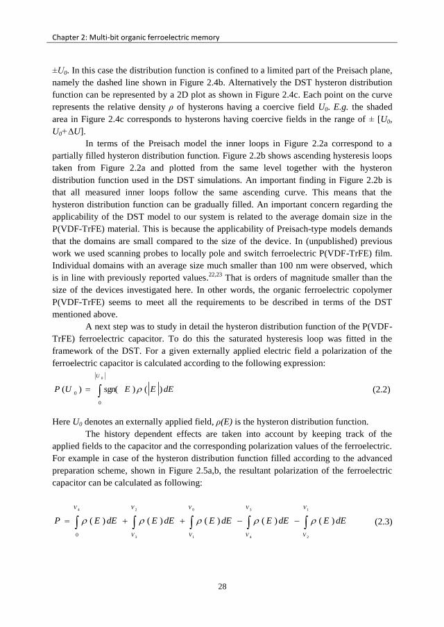
±U0. In this case the distribution function is confined to a limited part of the Preisach plane,
namely the dashed line shown in Figure 2.4b. Alternatively the DST hysteron distribution
function can be represented by a 2D plot as shown in Figure 2.4c. Each point on the curve
represents the relative density ρ of hysterons having a coercive field U0. E.g. the shaded
area in Figure 2.4c corresponds to hysterons having coercive fields in the range of ± [U0,
U0+∆U].
In terms of the Preisach model the inner loops in Figure 2.2a correspond to a
partially filled hysteron distribution function. Figure 2.2b shows ascending hysteresis loops
taken from Figure 2.2a and plotted from the same level together with the hysteron
distribution function used in the DST simulations. An important finding in Figure 2.2b is
that all measured inner loops follow the same ascending curve. This means that the
hysteron distribution function can be gradually filled. An important concern regarding the
applicability of the DST model to our system is related to the average domain size in the
P(VDF-TrFE) material. This is because the applicability of Preisach-type models demands
that the domains are small compared to the size of the device. In (unpublished) previous
work we used scanning probes to locally pole and switch ferroelectric P(VDF-TrFE) film.
Individual domains with an average size much smaller than 100 nm were observed, which
is in line with previously reported values.22,23
That is orders of magnitude smaller than the
size of the devices investigated here. In other words, the organic ferroelectric copolymer
P(VDF-TrFE) seems to meet all the requirements to be described in terms of the DST
mentioned above.
A next step was to study in detail the hysteron distribution function of the P(VDF-
TrFE) ferroelectric capacitor. To do this the saturated hysteresis loop was fitted in the
framework of the DST. For a given externally applied electric field a polarization of the
ferroelectric capacitor is calculated according to the following expression:
0
0
0)()sgn()(
U
dEEEUP (2.2)
Here U0 denotes an externally applied field, ρ(E) is the hysteron distribution function.
The history dependent effects are taken into account by keeping track of the
applied fields to the capacitor and the corresponding polarization values of the ferroelectric.
For example in case of the hysteron distribution function filled according to the advanced
preparation scheme, shown in Figure 2.5a,b, the resultant polarization of the ferroelectric
capacitor can be calculated as following:
1
2
3
4
0
1
2
3
4
)()()()()(
0
V
V
V
V
V
V
V
V
V
dEEdEEdEEdEEdEEP (2.3)

Dipole switching theory (DST)
29
Here the first three terms correspond to the parts of the hysteron distribution function filled
with positively oriented hysterons (up), whereas the last two terms ‒ to the negatively
oriented hysterons (down).
Figure 2.5: (a) Schematic representation of the hysteron distribution function filled according to the
preparation scheme in panel (b).
The dashed black curve in Figure 2.2a demonstrates the excellent quality of the
resulting fit; the corresponding hysteron distribution function is shown in Figure 2.2b. The
obtained hysteron distribution function was subsequently used for simulating the inner
hysteresis loops without any further parameter adjustments. The dashed curves in Figure
2.2a show the corresponding predicted inner polarization loops of the P(VDF-TrFE)
capacitor. Although the overall agreement is quite good, some systematic differences arise,
especially at intermediate applied voltages where the measured inner loops show larger
values for the saturated polarization as compared to the simulated loops. This is most likely
due to the broadening effect explained in Figure 2.4d: there is some fraction of hysterons
with coercive fields above the maximum applied field that is still switched, as well as some
(smaller) fraction of hysterons with coercive fields below the maximum applied field that
are not switched. In Figure 2.4d solid and dashed curves represent the switching charges
measured upon fully and partially inverting the polarization of a ferroelectric capacitor,
respectively. The solid line indicates the maximum applied voltage V0 used for partial
switching. Shaded light and shaded dark areas represent hysterons that are not switched
respectively additionally switched due to the broadening effect. This means that upon
partial poling the broadening effect significantly changes the shape and the integral of the
actual hysteron distribution function. Assuming a more or less constant shape of the
broadening function the largest difference between measured and simulated loops is
expected for inner loops close to the maximum of the hysteron distribution function. This is
indeed observed, as seen in the 3rd
curve, counted from the smallest loop, of Figure 2.2a.
Since the DST does not account for any broadening effects we can conclude that the
calculated data is in a good agreement with the experimental results.

Chapter 2: Multi-bit organic ferroelectric memory
30
2.2.3 Multi-bit states in P(VDF-TrFE)-based capacitor
A next step was to study in more detail the partial filling and reading of the
hysteron distribution function of the P(VDF-TrFE) ferroelectric capacitor. To do that a
specific polarization state of the ferroelectric was prepared and subsequently probed. Again
the quasi-static approach of the DWM was used. Figure 2.6a,b show the filling and probing
of the hysteron distribution function of the P(VDF-TrFE) ferroelectric capacitor. Colored
solid curves are the switching current of the ferroelectric capacitor as prepared by the
signals shown in the left insets. The first pulse of the preparation signal was used for
erasing previous memory effects and preparing a fully up (a) or down (b) polarized
ferroelectric capacitor. The second pulse of the preparation signal created the desired
polarization state of the ferroelectric. The right insets give a schematic representation of the
expected hysteron distribution functions as prepared by the corresponding preparation
signals. Positive and negative signs represent the two possible orientations of hysterons: up
or down. Colored vertical dashed lines correspond to the amplitude of the variable second
pulse of the preparation signal shown in the left insets.
To probe the created polarization state of the ferroelectric capacitor two probing
triangular pulses were used. In order to probe the state of the entire hysteron distribution the
amplitude of the probing pulses was chosen to be higher than the coercive voltage of the
ferroelectric capacitor. The sign of the readout pulse was such that hysterons switched in
the second preparation pulse are read out, i.e. are switched again and give rise to a current
response. It is important to stress that in this probing scheme hysterons with a polarization
state that corresponds to the first preparation pulse do not give a current response. Black
solid curves correspond to the switching of a fully polarized ferroelectric capacitor, i.e. the
Figure 2.6: Filling and probing a distribution function of a 200 nm thick Au/P(VDF-TrFE)/Au
ferroelectric capacitor. Colored solid curves describe the switching of the ferroelectric capacitor with
the distribution function filled with negatively oriented hysterons from the left (see Figure 2.6a) and
right side (see Figure 2.6b). Left insets: corresponding preparations signals. Right insets: schematic
representation of the resulting hysteron distribution functions. Colored dashed lines indicate the
amplitudes of the variable 2nd part of the preparation signals shown in the left insets.
Multi-bit states in P(VDF-TrFE)-based capacitor
31
largest amplitude of the second polarization pulse. The measured signals in Figure 2.6a,b
show that hysterons with low and high coercive fields can be poled in opposite directions:
the readout peak grows with the (magnitude of the) second preparation pulse, and,
importantly, maintains its shape with a maximum shifting to the higher (see panel a) or
lower voltage (see panel b). This means that the hysteron distribution function can indeed
be gradually filled as described in the right-side insets of Figure 2.6. It should also be noted
that the current traces in Figure 2.6 extend beyond the dashed lines, i.e. the magnitude of
the second preparation pulse. This is another manifestation of the broadening effect
discussed in Figures 2.2 and 2.4.
The important consequence of the data in Figure 2.6 is that the polarization of any
ferroelectric material that follows the DST can contain more information than just 'up' or
'down'. A well-known consequence is that the total polarization state of ferroelectrics can
be continuously tuned between full polarization in up and down directions. This underlies
the multi-level memory demonstrated in Ref. 12. However, the mean of a distribution does
not contain the full information. In particular, we shall demonstrate below that the
possibility to tailor the distribution function can be used to store multi-bit information in a
single memory element.
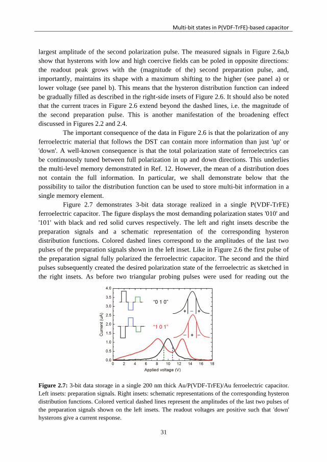
Figure 2.7 demonstrates 3-bit data storage realized in a single P(VDF-TrFE)
ferroelectric capacitor. The figure displays the most demanding polarization states '010' and
'101' with black and red solid curves respectively. The left and right insets describe the
preparation signals and a schematic representation of the corresponding hysteron
distribution functions. Colored dashed lines correspond to the amplitudes of the last two
pulses of the preparation signals shown in the left inset. Like in Figure 2.6 the first pulse of
the preparation signal fully polarized the ferroelectric capacitor. The second and the third
pulses subsequently created the desired polarization state of the ferroelectric as sketched in
the right insets. As before two triangular probing pulses were used for reading out the
Figure 2.7: 3-bit data storage in a single 200 nm thick Au/P(VDF-TrFE)/Au ferroelectric capacitor.
Left insets: preparation signals. Right insets: schematic representations of the corresponding hysteron
distribution functions. Colored vertical dashed lines represent the amplitudes of the last two pulses of
the preparation signals shown on the left insets. The readout voltages are positive such that 'down'
hysterons give a current response.
Chapter 2: Multi-bit organic ferroelectric memory
32
created polarization states of the ferroelectric. Clearly '010' and '101' preparation pulses
give rise to well distinguishable peaks and valleys at the anticipated positions: the data
storage is binary. Hence three bits of information can be stored in such single memory
element.
Although the same ramping speed in the readout pulses was used in Figures 2.6
and 2.7, the current signal in the latter was much reduced. The reason is the broadening
effect discussed before. Especially in the '101' response (red line) it is clear that the middle
part of the distribution function not completely separates the outer two. Since the probing
scheme measures, at each point in the distribution function, the difference between the up
and down fractions, this leads to the observed signal reduction. As a consequence, the '010'
state cannot be obtained unambiguously by subtraction of the '101' state from the '111' state
in our device. The latter corresponds to the fully switched ferroelectric polarization shown
by the black lines in Figure 2.6 a and b. In passing we also note that the lowest peaks in
Figure 2.6 (green in panel a and red in b) correspond to the '100' and '001' signals.
Finally, we should address some practical aspects of these devices. First, these
devices were not optimized in any way. Au and P(VDF-TrFE) were taken for ease of
fabrication and availability. However, P(VDF-TrFE) is known for its excellent retention
and great environmental stability. All programmed signals were stable over at least several
tens of hours suggesting that the hysteron distribution function is time stable. Moreover all
measured devices showed good state reproducibility, as may be expected from the simple
processing, and therefore may be expected to have a potentially great scalability.
2.3 Conclusions
In summary, we have introduced multi-bit data storage with binary readout from a
simple capacitor structure. The working principle of our multi-bit device is completely
general and only demands the applicability of the dipole switching theory (DST). The DST
considers ferroelectric material as a collection of micro dipoles (hysterons) described by a
specific Preisach distribution function. We showed experimentally that the organic
ferroelectric copolymer P(VDF-TrFE) meets all the requirements to be described in terms
of the DST. All basic ferroelectric properties together with the hysteron distribution
function of P(VDF-TrFE) ferroelectric capacitors were studied using the quasi-static
double-wave method. In addition, ferroelectric properties of the device were modeled in the
framework of the DST. Finally, we demonstrate a 3-bit data storage element. As a first
example we show the possibility to independently program and subsequently read out the
lower, middle and upper parts of the hysteron distribution function, yielding a 3-bit memory
in a single capacitor structure. All measured devices show good state reproducibility, high
endurance and potentially great scalability. Hence we expect that our findings will be

Experimental
33
interesting for the realization of multi-bit organic ferroelectric-based memories for low-cost
large area electronics.
2.4 Experimental
Poly(vinylidene fluoride-trifluoroethylene P(VDF-TrFE) (Mn = 220 kDa, 2.3 < D
< 2.8 with a 77/23 VDF/TrFE ratio) was supplied by Solvay Specialty Polymers. Devices
were made by spin-coating a 200 nm thick film of P(VDF-TrFE) ferroelectric polymer on
top of glass substrates with patterned gold electrodes: 1.2 × 1.2 mm2, 700 × 700 µm
2, 400 ×
400 µm2, 250 × 250 µm
2. After spin coating, the films were annealed for 1 hour at 135 °C
followed by the deposition of the top Au electrode thorough a shadow mask. Using surface
profilometry the layer thickness of the P(VDF-TrFE) was determined to be ≈ 200 ± 10 nm.
P-V characteristics and the properties of the hysteron distribution function were measured
using an Agilent function generator 33120A (source), an external high speed voltage
amplifier Falco Systems WMA-300 and a Keithley picoammeter 6485 (sense).
2.5 References
[1] H.-S. P. Wong, S. Raoux, S. Kim, J. Liang, J.P. Reifenberg, B. Rajendran, M. Asheghi,
K.E. Goodson, Phase change memory, P. IEEE 2010, 98, 2201.
[2] F. Verbakel, S.C.J. Meskers, R.A.J. Janssen, H.L. Gomes, M. Cölle, M. Büchel, D.M. de
Leeuw, Reproducible resistive switching in nonvolatile organic memories, Appl. Phys. Lett.
2007, 91, 192103.
[3] M. Cölle, M. Büchel, D.M. de Leeuw, Switching and filamentary conduction in non-
volatile organic memories, Org. Electron. 2006, 7, 305.
[4] Q.-D. Ling, D.-J. Liaw, C. Zhu, D.S.-H. Chan, E.-T. Kang, K.-G. Neoh, Polymer electronic
memories: materials, devices and mechanisms, Prog. Polym. Sci. 2008, 33, 917.
[5] P. Heremans, G. H. Gelinck, R. Müller, K.-J. Baeg, D.-Y. Kim, Y.-Y. Noh, Polymer and
organic nonvolatile memory devices, Chem. Mater. 2011, 23, 341-358.
[6] B.H. Park, B.S. Kang, S.D. Bu, T.W. Noh, J. Lee, W. Jo, Lanthanum-substituted bismuth
titanate for use in non-volatile memories, Nature 1999, 401, 682.
[7] I. Jung, J.Y. Son, A nonvolatile memory device made of a grapheme nanoribbon and a
multiferroic BiFeO3 gate dielectric layer, Carbon 2012, 50, 3854.
[8] I. Stolichnov, S.W.E. Riester, H.J. Trodahl, N. Setter, A.W. Rushforth, K.W. Edmonds,
R.P. Campion, C.T. Foxon, B.L. Gallagher, T. Jungwirth, Non-volatile ferroelectric control
of ferromagnetism in (Ga,Mn)As, Nat. Mater. 2008, 7, 464.
[9] T. Kawahara, K. Ito, R. Takemura, H. Ohno, Spin-transfer torque RAM technology: review
and prospect, Microelectron. Reliab. 2012, 52, 613.
[10] R.C. Sousa, I.L. Prejbeanu, Non-volatile magnetic random access memories (MRAM), C.
R. Phys. 2005, 6, 1013.

Chapter 2: Multi-bit organic ferroelectric memory
34
[11] A.K. Tripathi, A.J..J.M. van Breemen, J. Chen, Q. Gao, M.G. Ivan, K. Reimann, E.R.
Meinders, G.H. Gelinck, Multilevel information storage in ferroelectric polymer memories,
Adv. Mater. 2011, 23, 4146.
[12] D. Lee, S.M. Yang, T.H. Kim, B.C. Jeon, Y.S. Kim, J.-G. Yoon, H.N. Lee, S.H. Baek, C.B.
Eom, T.W. Noh, Multilevel data storage memory using deterministic polarization control,
Adv. Mater. 2012, 24, 402.
[13] L. Wang, J. Yu, Y. Wang, G. Peng, F. Liu, J. Gao, Modeling ferroelectric capacitors based
on the dipole switching theory, J. Appl. Phys. 2007, 101, 104505.
[14] F. Yang, M.H. Tang, Y.C. Zhou, X.J. Zheng, F. Liu, J.X. Tang, J.J. Zhang, J. Zhang, C.Q.
Sun, A model for the polarization hysteresis loops of the perovskite-type ferroelectric thin
films, Appl. Phys. Lett. 2007, 91, 142902.
[15] C.H. Tsang, C.K. Wong, F.G. Shin, Modeling saturated and unsaturated ferroelectric
hysteresis loops: An analytical approach, J. Appl. Phys. 2005, 98, 084103.
[16] Y.J. Park, J. Chang, S.J. Kang, C. Park, Polarization retention of thin ferroelectricya
capacitors, Appl. Phys. Lett. 2009, 95, 102902.
[17] K.-H. Kim, Properties of ferroelectric VDF-TrFE copolymer capacitors directly deposited
on Si wafers, J. Korean Phys. Soc. 2008, 52, 88.
[18] M. Fukunaga, Y. Noda, Improvement of the double-wave method for ferroelectric
hysteresis loops and its application to multiferroic EuMn2O5, J. Korean Phys. Soc. 2009,
55, 888.
[19] M. Fukunaga, Y. Noda, New technique for measuring ferroelectric and antiferroelectric
hysteresis loops, J. Phys. Soc. Jpn. 2008, 77, 064706.
[20] N. Tsutsumi, X. Bai, W. Sakai, Towards nonvolatile memory devices based on ferroelectric
polymers, AIP Adv. 2012, 2, 012154.
[21] S.L. Miller, J.R. Schwank, R.D. Nasby, M.S. Rodgers, Modeling ferroelectric capacitor
switching with asymmetric nonperiodic input signals and arbitrary initial conditions, J.
Appl. Phys. 1991, 70, 2849.
[22] B.J. Rodriguez, S. Jesse, S.V. Kalinin, J. Kim, S. Ducharme, V.M. Fridkin, Nanoscale
polarization manipulation and imaging of ferroelectric Langmuir-Blodgett polymer films,
Appl. Phys. Lett. 2007, 90, 122904.
[23] P. Sharma, T. Nakajima, S. Okamura, A. Gruverman, Effect of disorder potential on
domain switching behavior in polymer ferroelectric films, Nanotechnology 2013, 24,
015706.

35
Chapter 3
Nanoscale ferroelectric diodes
Ferroelectric diodes function by grace of nanoscale phase separation in a blend of
a semiconducting and a ferroelectric polymer that is sandwiched between metallic
electrodes. In this chapter, various scanning probe techniques are combined with
numerical modeling to unravel their operational mechanism. Resistive switching is shown
to result from modulation of the charge injection barrier at the semiconductor-electrode
interfaces. The modulation is driven by the stray field of the polarization charges in the
ferroelectric phase, and consequently is restricted to regions where semiconductor and
ferroelectric phases exist in close vicinity. Since each semiconductor domain can
individually be switched and read out a novel, nanoscale memory element is demonstrated.
An ultimate information density of ≈ 30 Mb/cm2 is estimated for this bottom-up defined
memory device.
Published as:
V. Khikhlovskyi, R. Wang A.J.J.M. van Breemen, G.H. Gelinck, R.A.J. Janssen, and M. Kemerink,
Nanoscale Organic Ferroelectric Resistive Switches, J. Phys. Chem. C 2014, 118, 3305-3312.

Chapter 3: Nanoscale organic ferroelectric resistive switches
36
3.1 Introduction
There exists an ongoing and actually increasing search for novel, non-volatile
memory elements. Any viable novel technology in this direction should offer low cost, easy
processing, high on/off ratio, scalability, good endurance and easy readout. For the latter, it
is strongly preferred to read the (binary) data directly in the form of a high or low current or
resistance, rather than indirectly via e.g. detection of a (lack of) response of a polarization
switching pulse. The simplest and cheapest resistance readout scheme, the crossbar array,
puts the additional constraint on the memory element that it has to be rectifying in order to
prevent crosstalk between neighboring bits.1 For these reasons significant efforts have been
directed at inorganic multiferroic/ferroelectric materials such as BiFeO3 (BFO). In these
materials the polarization state directly affects the resistance of the device.2,3
It was recently
demonstrated that lithographically defined ≈ 70 nm sized pillars of BFO could be
individually switched and read out.4 Also metal oxide memristors of reduced size were
demonstrated5; it should however be noted that some of these devices do not rectify and
consequently need additional electronic components in the readout scheme. A major
drawback of many such inorganic devices is the need for advanced materials engineering
and complicated device fabrication.6,7
Very recently it was shown that 100 nm sized pillars
of the organic ferroelectric P(VDF-TrFE) could be created by an imprinting process and
could be ferroelectrically switched and read out by a scanning probe tip.8 Due to the
insulating nature of P(VDF-TrFE) these structures cannot be read out resistively.
An extremely promising alternative was recently proposed by Asadi et al., who
showed in a series of papers that thin, phase separated films of a blend of a ferroelectric and
a semiconducting polymer fulfill the criteria listed above. A major advantage of this
approach is that the (ferroelectric) switching and (resistive) readout functionalities are
distributed over different materials and consequently can be individually optimized.9,10
The
crucial ability to downscale the bit size was, however, not experimentally addressed.
Moreover, the operational mechanism has so far remained disputed.11
The structure and the proposed working principle of the device are described in
Chapter 1. It has to be noted that the ferroelectric diode makes it possible to combine the
key properties of the ferroelectrics (non-volatile data storage) with the beneficial properties
of the semiconductors (conductivity/rectification) in one device. Such fully organic
rewritable memory element has great potential for memory applications as it can be driven
in a simple crossbar array.12
In this chapter, we address the related questions regarding the unknown
operational mechanism of these devices, and their minimal bit size. We demonstrate that
the resistivity of individual, nanosized semiconductor domains can be switched and read
out. In contrast to their inorganic counterparts, these nanostructures spontaneously form in
a bottom-up process – spinodal decomposition during film drying.13
In addition, our results
prove that the stray field of the ferroelectric polarization effectively in- or decreases the

Morphology and ferroelectric properties of the blend at the local scale
37
injection barrier in the vicinity of the semiconductor/ferroelectric interface. The modulation
of theinjection barrier translates into the resistance modulation that is used for read out.
These findings point at an interesting parallel between the present organic devices and the
switching in inorganic BFO diodes: in both cases the ferroelectric polarization modulates a
Schottky-like injection barrier.4,11
3.2 Results and discussion
3.2.1 Morphology and ferroelectric properties of the blend at the local
scale
The active layer in this work is formed by a continuous film of a 1:9 wt/wt blend
of F8BT and P(VDF-TrFE). The film was spincoated on top of glass substrates with
patterned gold electrodes and annealed at 135 °C for 1 hour to enhance the crystallinity of
the ferroelectric phase. Using surface profilometry we determined the layer thickness of the
P(VDF-TrFE):F8BT blend to be ≈ 200 nm.
First, the morphology and the ferroelectric properties of the P(VDF-TrFE):F8BT
blend at the nanoscale were characterized. The switching voltage of a capacitor with this
layer thickness, based solely on the ferroelectric component of the blend, was found at ≈
|10| V. This corresponds to a coercive field (EC) of approximately 50 MV/m of the
ferroelectric polymer.14
Figure 3.1a shows a typical topography of a ferroelectric diode
without the top electrode obtained by atomic force microscopy (AFM). The topography
image clearly shows that the blend consists of round, 300 – 750 nm sized semiconducting
(F8BT) domains in a homogeneous crystalline ferroelectric P(VDF-TrFE) matrix, in line
with previous observations using other polymer semiconductors.13,15
Both semiconducting
and ferroelectric phases are essentially pure, i.e. phase separation is (almost) 100 %.13
The
thickness of the inner part of the F8BT domains is in most cases less than the thickness at
the perimeter, i.e. most domains are concave. In order to probe the ferroelectric properties
of the blend, the inner part (10 × 10 µm2) of Figure 3.1a was polarized by applying – 15 V
(i.e. above the coercive voltage of ≈ |10| V of the ferroelectric film) to the AFM tip while
scanning in contact-mode. Figure 3.1b shows the corresponding piezoresponse force
microscopy (PFM) image of the complete area after poling. The dark region of the image
corresponds to the polarized region, oriented from the bottom contact to the surface of the
blend. The PFM signal comes only from the ferroelectric phase of the blend, not from the
semiconducting phase of the blend. In general, written patterns were stable over at least
several tens of hours meaning that the depolarization effects16-18
are negligible on this time-
scale. Scanning with a reverse bias (e.g. + 15 V) inverted the polarization state (not shown).
We find that the devices can be reversibly switched by AFM for many cycles without
noticeable traces of degradation.
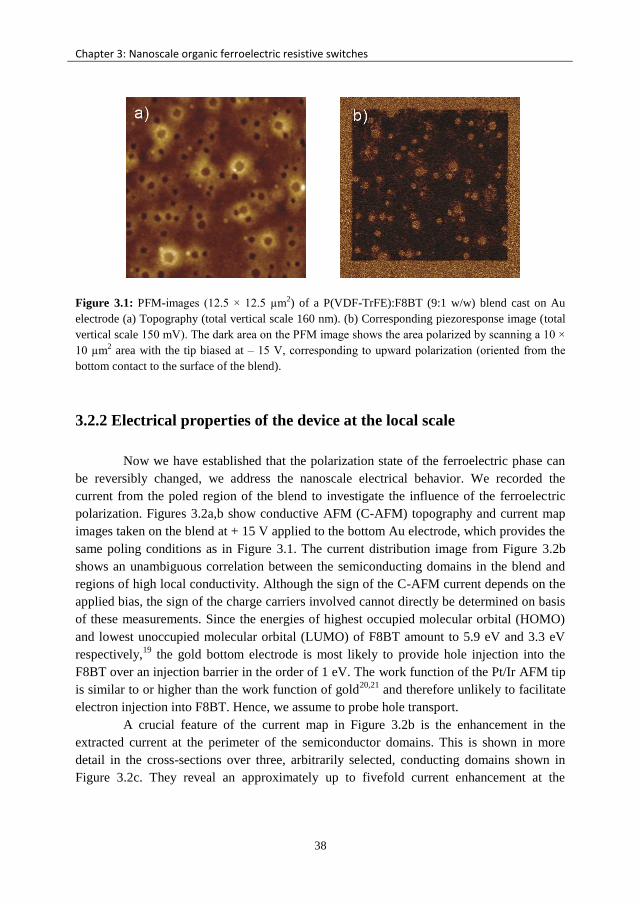
Chapter 3: Nanoscale organic ferroelectric resistive switches
38
Figure 3.1: PFM-images (12.5 × 12.5 µm2) of a P(VDF-TrFE):F8BT (9:1 w/w) blend cast on Au
electrode (a) Topography (total vertical scale 160 nm). (b) Corresponding piezoresponse image (total
vertical scale 150 mV). The dark area on the PFM image shows the area polarized by scanning a 10 ×
10 µm2 area with the tip biased at ‒ 15 V, corresponding to upward polarization (oriented from the
bottom contact to the surface of the blend).
3.2.2 Electrical properties of the device at the local scale
Now we have established that the polarization state of the ferroelectric phase can
be reversibly changed, we address the nanoscale electrical behavior. We recorded the
current from the poled region of the blend to investigate the influence of the ferroelectric
polarization. Figures 3.2a,b show conductive AFM (C-AFM) topography and current map
images taken on the blend at + 15 V applied to the bottom Au electrode, which provides the
same poling conditions as in Figure 3.1. The current distribution image from Figure 3.2b
shows an unambiguous correlation between the semiconducting domains in the blend and
regions of high local conductivity. Although the sign of the C-AFM current depends on the
applied bias, the sign of the charge carriers involved cannot directly be determined on basis
of these measurements. Since the energies of highest occupied molecular orbital (HOMO)
and lowest unoccupied molecular orbital (LUMO) of F8BT amount to 5.9 eV and 3.3 eV
respectively,19
the gold bottom electrode is most likely to provide hole injection into the
F8BT over an injection barrier in the order of 1 eV. The work function of the Pt/Ir AFM tip
is similar to or higher than the work function of gold20,21
and therefore unlikely to facilitate
electron injection into F8BT. Hence, we assume to probe hole transport.
A crucial feature of the current map in Figure 3.2b is the enhancement in the
extracted current at the perimeter of the semiconductor domains. This is shown in more
detail in the cross-sections over three, arbitrarily selected, conducting domains shown in
Figure 3.2c. They reveal an approximately up to fivefold current enhancement at the
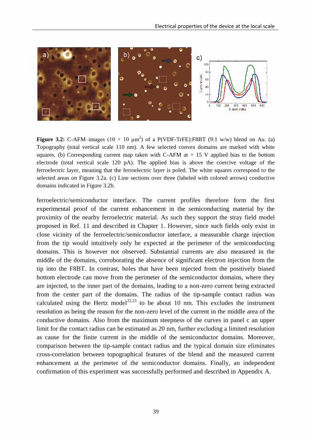
Electrical properties of the device at the local scale
39
Figure 3.2: C-AFM–images (10 × 10 µm2) of a P(VDF-TrFE):F8BT (9:1 w/w) blend on Au. (a)
Topography (total vertical scale 110 nm). A few selected convex domains are marked with white
squares. (b) Corresponding current map taken with C-AFM at + 15 V applied bias to the bottom
electrode (total vertical scale 120 pA). The applied bias is above the coercive voltage of the
ferroelectric layer, meaning that the ferroelectric layer is poled. The white squares correspond to the
selected areas on Figure 3.2a. (c) Line sections over three (labeled with colored arrows) conductive
domains indicated in Figure 3.2b.
ferroelectric/semiconductor interface. The current profiles therefore form the first
experimental proof of the current enhancement in the semiconducting material by the
proximity of the nearby ferroelectric material. As such they support the stray field model
proposed in Ref. 11 and described in Chapter 1. However, since such fields only exist in
close vicinity of the ferroelectric/semiconductor interface, a measurable charge injection
from the tip would intuitively only be expected at the perimeter of the semiconducting
domains. This is however not observed. Substantial currents are also measured in the
middle of the domains, corroborating the absence of significant electron injection from the
tip into the F8BT. In contrast, holes that have been injected from the positively biased
bottom electrode can move from the perimeter of the semiconductor domains, where they
are injected, to the inner part of the domains, leading to a non-zero current being extracted
from the center part of the domains. The radius of the tip-sample contact radius was
calculated using the Hertz model22,23
to be about 10 nm. This excludes the instrument
resolution as being the reason for the non-zero level of the current in the middle area of the
conductive domains. Also from the maximum steepness of the curves in panel c an upper
limit for the contact radius can be estimated as 20 nm, further excluding a limited resolution
as cause for the finite current in the middle of the semiconductor domains. Moreover,
comparison between the tip-sample contact radius and the typical domain size eliminates
cross-correlation between topographical features of the blend and the measured current
enhancement at the perimeter of the semiconductor domains. Finally, an independent
confirmation of this experiment was successfully performed and described in Appendix A.

Chapter 3: Nanoscale organic ferroelectric resistive switches
40
Figure 3.3: C-AFM–images (10 × 10 µm2) of a F8BT on Au. (a) Topography (total vertical scale 20
nm). (b) Corresponding current map at + 20 V applied bias (total vertical scale 0.8 pA). The C-AFM
image shows no current above the sensitivity of the C-AFM setup (≈ 1 pA).
To exclude the possibility that the current in Figure 3.2b is due to the large field at
the apex of the tip24,25
and not related to the ferroelectric polarization, the same
measurements were done on pure F8BT films. In case of pure F8BT there is no sign of any
current above the sensitivity (≈ 1 pA) of the C-AFM setup, even at larger applied voltages
(see Figure 3.3).
An important finding in Figure 3.2a,b is the fact that most convex domains carry
no measurable current and the concave domains are mainly responsible for the current in
the device. In the convex domains the current is most likely blocked by a thin layer of
P(VDF-TrFE). Because P(VDF-TrFE) is an excellent insulator, a 10 nm thick P(VDF-
TrFE) film would be sufficient for complete blocking of the charge transfer. From an
application point of view, the non-contributing convex domains are to be avoided. To
analyze this in more detail, additional AFM images of the blend on smaller areas were
recorded in tapping (or intermittent contact) mode (TM). Figure 3.4a shows a few convex
and concave domains marked with circles and squares respectively. Since TM-AFM phase
imaging provides detailed nanometer-scale information about surface visco-elastic
properties it can readily detect variations in top layer composition. The TM-AFM phase
image shown in Figure 3.4b shows a clear contrast between F8BT (dark) and the stiffer
(bright) regions of the crystallized P(VDF-TrFE) in both convex and the concave domains.
This strongly suggests that the top surface in all domains consists of F8BT. In the convex
domains the F8BT phase does not extend all the way down to the bottom electrode but is
effectively interrupted by a buried layer of P(VDF-TrFE).
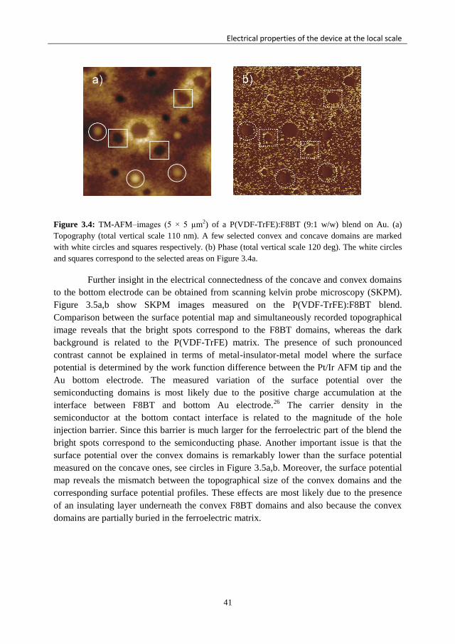
Electrical properties of the device at the local scale
41
Figure 3.4: TM-AFM–images (5 × 5 µm2) of a P(VDF-TrFE):F8BT (9:1 w/w) blend on Au. (a)
Topography (total vertical scale 110 nm). A few selected convex and concave domains are marked
with white circles and squares respectively. (b) Phase (total vertical scale 120 deg). The white circles
and squares correspond to the selected areas on Figure 3.4a.
Further insight in the electrical connectedness of the concave and convex domains
to the bottom electrode can be obtained from scanning kelvin probe microscopy (SKPM).
Figure 3.5a,b show SKPM images measured on the P(VDF-TrFE):F8BT blend.
Comparison between the surface potential map and simultaneously recorded topographical
image reveals that the bright spots correspond to the F8BT domains, whereas the dark
background is related to the P(VDF-TrFE) matrix. The presence of such pronounced
contrast cannot be explained in terms of metal-insulator-metal model where the surface
potential is determined by the work function difference between the Pt/Ir AFM tip and the
Au bottom electrode. The measured variation of the surface potential over the
semiconducting domains is most likely due to the positive charge accumulation at the
interface between F8BT and bottom Au electrode.26
The carrier density in the
semiconductor at the bottom contact interface is related to the magnitude of the hole
injection barrier. Since this barrier is much larger for the ferroelectric part of the blend the
bright spots correspond to the semiconducting phase. Another important issue is that the
surface potential over the convex domains is remarkably lower than the surface potential
measured on the concave ones, see circles in Figure 3.5a,b. Moreover, the surface potential
map reveals the mismatch between the topographical size of the convex domains and the
corresponding surface potential profiles. These effects are most likely due to the presence
of an insulating layer underneath the convex F8BT domains and also because the convex
domains are partially buried in the ferroelectric matrix.

Chapter 3: Nanoscale organic ferroelectric resistive switches
42
Figure 3.5: AFM-SKPM–images (5 × 5 µm2) of a P(VDF-TrFE):F8BT (9:1 w/w) blend on Au (a)
Topography (total vertical scale 110 nm). Two selected convex domains are marked with white
circles. (b) Corresponding surface potential map (total vertical scale 0.2 V). The white circles
correspond to the selected areas on Figure 3.5a.
3.2.3 Modeling of the electrical properties of the device at the local scale
In order to interpret the measurements presented above in more detail a 2D model
of the ferroelectric diode was developed. The phase separated morphology is simplified to a
2D structure of alternating ferroelectric and semiconducting slabs (see Figure 1.5c, Chapter
1). Motion of electrons and holes is described by the transport, continuity and Poisson
equations that are numerically solved on a rectangular grid.11,27,28
The parameters of the
blend used in the simulation and the electrical transport model are explained in detail in the
Experimental Section and Appendix A respectively.
First the C-AFM measurements were simulated. A 2D representation of the
current distribution in a single semiconducting domain shows that the charge carriers are
injected at the ferroelectric/semiconductor interface in agreement with the stray field model
(see Figure 3.6). Figure 3.7a shows a joint plot of the measured and the simulated C-AFM
data. The colored dotted curves represent normalized C-AFM current line sections
measured over five randomly chosen semiconducting domains with a diameter of about 450
nm. The simulated current profile is shown by the black solid curve. There is good
agreement between calculated and measured data. Note in particular that the nonzero
current in the middle of the semiconductor domain discussed above is reproduced by the
simulation. Hence, we conclude that the stray field model is an accurate description of the
device operation.
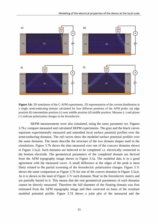
Modeling of the electrical properties of the device at the local scale
43
Figure 3.6: 2D simulation of the C-AFM experiments. 2D representation of the current distribution in
a single semiconducting domain calculated for four different positions of the AFM probe: (a) edge
position (b) intermediate position (c) near middle position (d) middle position. Minuses (‒) and pluses
(+) indicate polarization charges in the ferroelectric.
SKPM measurements were also simulated, using the same parameter set. Figures
3.7b,c compare measured and calculated SKPM experiments. The gray and the black curves
represent experimentally measured and smoothed local surface potential profiles over the
semiconducting domains. The red curves show the modeled surface potential profiles over
the same domains. The insets describe the structure of the two domain shapes used in the
simulations. Figure 3.7b shows the data measured over one of the concave domains shown
in Figure 3.5a,b. Such domains are believed to be completed i.e. electrically connected to
the bottom electrode. The geometrical parameters of the completed domain are derived
from the AFM topography image shown in Figure 3.5a. The modeled data is in a good
agreement with the measured curve. A small difference at the edges of the peak is most
likely related to the partial screening of the ferroelectric polarization charges. Figure 3.7c
shows the same comparison as Figure 3.7b for one of the convex domains in Figure 3.5a,b.
As it is shown in the inset of Figure 3.7c such domains 'float' in the ferroelectric matrix and
are partially buried in it. This means that the real geometrical parameters of such domains
cannot be directly measured. Therefore the full diameter of the floating domain was first
estimated from the AFM topography image and then corrected on basis of the resultant
modeled potential profile. Figure 3.7d shows a joint plot of the measured and the

Chapter 3: Nanoscale organic ferroelectric resistive switches
44
Figure 3.7: Measured and simulated C-AFM and SKPM experiments. (a) Normalized current line
sections over five typical conductive domains with a diameter of about 450 nm are shown (different
colored symbols). The black line is the calculated profile. (b) Measured and smoothed surface
potential profiles over one of the completed domains shown by gray and black curves respectively.
The calculated profile is shown in red. The inset shows the structure of the semiconducting domain
embedded in the ferroelectric. (c) As panel b for a floating domain. The geometrical parameters of the
domain used in the simulation are shown in the right inset. The full diameter and undercut of the
domain, are 500 nm and 75 nm, respectively, as shown in the right inset. The topographically
estimated diameter is 350 nm. (d) Joint plot of the measured and the calculated potential profiles over
the floating semiconducting domain. The black curve is the experimentally obtained smoothed
potential profile. Red and green curves represent the modeled potential profiles based on the
topographically estimated and corrected geometrical parameters of the semiconducting domain,
respectively. The geometrical parameters of the domain used in the simulation are the same as in (c).
calculated potential profiles. The modeled curves are based on both the estimated and the
corrected diameters of the semiconducting domains. Thus, the SKPM measurements
confirm the structure of the floating semiconducting domains found from the C-AFM and
the TM-AFM measurements.

Single domain poling
45
3.2.4. Single domain poling
Using local probing techniques we can investigate the limits of the attainable bit
density. Figure 3.8 shows that individual domains can potentially be used as individual
information storing bits. The white arrow on the topography image (see Figure 3.8a) points
to the domain which was chosen for individual poling. A poling voltage of + 16 V was
used. The dark area on the piezoresponse image, Figure 3.8b, shows that the area around
this domain has been selectively poled with upward polarization. Figure 3.8c presents the
current map. The selected domain displays clear current enhancement as a result of the
ferroelectric poling of the surrounding P(VDF-TrFE) matrix. In passing we note that this
experimentally confirms that the current switching by the lowering of the effective injection
barrier is only driven by the ferroelectric polarization charges in the immediate vicinity of
the semiconductor/ferroelectric interface.
Figure 3.8: PFM– and C-AFM–images (4 × 3.5 µm2) of a P(VDF-TrFE):F8BT (9:1 w/w) blend on
Au after selective poling around a single domain (indicated by the arrow). (a) Topography (total
vertical scale 110 nm). (b) Corresponding piezoresponse image (total vertical scale 120 mV). (c)
Corresponding current map, subsequently taken with C-AFM at + 6 V bias applied to the back contact
(total vertical scale 10 pA).
For the investigated blend, 300 nm is the approximate lower limit on the attainable
feature size of the semiconducting domains. Since the writing resolution of ca. 100 nm is
smaller than this value, the ultimate data density can be estimated as 1/4×F2, with F the
feature size of 300 nm.11
Note that this feature size is achieved in an electrical readout
scheme and is virtually identical to the feature size achieved by Chen et al. by reading and
writing the polarization state of ferroelectric nano-pillars by PFM.8 Thus, for a memory
crossbar array with properly aligned semiconducting domains at the intersections between
word and bit lines a rewritable information density of the order of 30 Mb/cm2 could in
principle be achieved.

Chapter 3: Nanoscale organic ferroelectric resistive switches
46
3.3 Conclusions
In summary, we have studied the operating mechanism of ferroelectric diodes
based on a phase separated blend of ferroelectric and semiconducting polymers at the
nanometer scale by a combination of SPM techniques and numerical modeling. We
measure a direct correlation between the extracted current from the semiconducting
domains and the polarization state of the ferroelectric surrounding the domains. Device
operation is therefore intimately linked to the phase separated morphology. Depending on
the local polarization state of the P(VDF-TrFE) matrix surrounding a specific domain, the
current in that semiconductor domain is enhanced or not. The fact that the current density
was found to be higher at the perimeter of the semiconductor domains is unambiguous
proof that charges are predominantly injected at the perimeter of the domains. These results
are therefore in line with the proposed theoretical model that the stray field of the
polarization charges in the ferroelectric phase can modulate charge injection from the
electrode into the semiconductor in the regions where semiconductor and ferroelectric
phases exist in close vicinity.
Moreover, we have proven that the semiconductor domains can be individually
addressed, both in writing and reading. As such, each domain can be regarded as a bottom-
up nanosized memory element. For the present blends this translates into a potential
maximum memory density in the order of 30 Mb/cm2, enough for low-cost applications
based on printed electronics.
It is, finally, interesting to point out that the operational mechanism of the present
ferroelectric diodes is extremely similar to the proposed mechanism of memory diodes
based on inorganic ferroelectric materials as BiFeO3. In both cases the ferroelectric
polarization charges modulate the Schottky-like barrier for charge injection into the
conducting phase.4,11
3.4 Experimental
Poly(vinylidene fluoride-trifluoroethylene) P(VDF-TrFE) (Mn = 220 kDa, 2.3 < D
< 2.8 with a 77/23 VDF/TrFe ratio) was supplied by Solvay Specialty Polymers. Poly[(9,9-
di-n-octylfluorenyl-2,7-diyl)-alt-(benzo[2,1,3]thiadiazol-4,8-diyl)] F8BT (Mn = 13 kDa, D
= 2.0) was synthesized according to a modified Suzuki-polymerization.29,30
Devices were
made by spin-coating a 200 ± 10 nm thick film of a 9:1 w/w P(VDF-TrFE):F8BT blend on
top of glass substrates with patterned gold electrodes. After spin coating, the films were
annealed for 1 hour at 135 °C. Since SPM techniques require a direct contact of the probe
with the studied material the deposition of the top contact was omitted meaning that the
AFM tip served as a top electrode.
Conductive atomic force microscopy (C-AFM), piezoresponse force microscopy
(PFM) and scanning kelvin probe microscopy (SKPM) are employed to locally probe

Experimental
47
current pathways, polarization states and electrostatic potentials, respectively. The C-AFM,
PFM and SKPM schemes were implemented on a commercial AFM system (Veeco
MultiMode NS-IIIA) equipped with an external signal generator/lock-in amplifier. The C-
AFM and the PFM measurements were performed using Pt/Ir coated Si tips (Nanosensors,
spring constant k ≈ 5 N/m). The PFM images were acquired using a modulation voltage of
2 Vp.p. at a frequency of 100 kHz, i.e. well below the first contact resonance. All SPM
measurements were performed under ambient conditions. The C-AFM current was detected
using a high sensitivity current amplifier (TUNA module, 1011
V/A, Veeco). In our setup,
C-AFM and PFM could be switched easily without disturbing the alignment of the AFM
tip, allowing in situ conductivity and polarization characterization of the same area. The
surface potential map was measured using Al coated Si tips (Nanosensors, spring constant k
≈ 12.5 N/m).
The employed 2D model for ferroelectric diodes takes into account the phase
separated morphology. The ferroelectric P(VDF-TrFE) is characterized by a zero mobility
because of its insulating properties. In the ferroelectric slab a surface polarization charge
density σp ≈ 70 mC/m2 is fixed on the first grid points, 2 nm above the bottom electrode and
below the top surface of the blend. A static relative dielectric constant εr = 10 was used. The
organic semiconducting slab F8BT was characterized by a typical (constant) hole mobility,
µp = 6.5×10⁻¹¹
m2/(V·s) and εr = 3. The LUMO and the HOMO levels of the semiconductor
are set at around 3.3 eV and 5.9 eV respectively. The hole injection barrier at the bottom
electrode is fixed at 0.9 eV. The work function of the AFM probe is estimated to be around
5.6 eV. A field-dependent charge injection into the semiconductor is implemented by using
the Emtage/O’Dwyer model.31,32
3.5 References
[1] K. Asadi, M. Li, P.W.M. Blom, M. Kemerink, D.M. de Leeuw, Organic ferroelectric opto-
electronic memories, Mater. Today 2011, 14, 592.
[2] T. Choi, S. Lee, Y.J. Choi, V. Kiryukhin, S.-W. Cheong, Switchable ferroelectric diode and
photovoltaic, Science 2009, 324, 63.
[3] A.Q. Jiang, C. Wang, K.J. Jin, X.B. Liu, J.F. Scott, C.S. Hwang, T.A. Tang, H.B. Lu, G.Z.
Yang, A resistive memory in semiconducting BiFeO3 thin-film capacitors, Adv. Mater.
2011, 23, 1277.
[4] S. Hong, T. Choi, J.H. Jeon, Y. Kim, H. Lee, H.-Y. Joo, I. Hwang, J.-S. Kim, S.-O. Kang,
S.V. Kalinin, B.H. Park, Large resistive switching in ferroelectric BiFeO3 nano-island based
switchable diodes, Adv. Mater. 2013, 25, 2339.
[5] D.J. Kim, H. Lu, S. Ryu, C.-W. Bark, C.-B. Eom, E.Y. Tsymbal, A. Gruverman,
Ferroelectric tunnel memristor, Nano Lett. 2012, 12, 5697.
[6] J. Mannhart, D.G. Schlom, Oxide interfaces – an opportunity for electronics, Science 2010,
327, 1607.
[7] S.D. Ha, S. Ramanathan, Adaptive oxide electronics: A review, J. Appl. Phys. 2011, 110,
071101.
Chapter 3: Nanoscale organic ferroelectric resistive switches
48
[8] X.-Z. Chen, Q. Li, X. Chen, X. Guo, H.-X. Ge, Y. Liu, Q.-D. Shen, Nano-imprinted
ferroelectric polymer nanodot arrays for high density data storage, Adv. Funct. Mater. 2013,
23, 3124.
[9] K. Asadi, D.M. de Leeuw, B. de Boer, P.W.M. Blom, Organic non-volatile memories from
ferroelectric phase- separated blends, Nat. Mater. 2008, 7, 547.
[10] K. Asadi, T.G. de Boer, P.W.M. Blom, D.M. de Leeuw, Tunable injection barrier in organic
resistive switches based on phase-separated ferroelectric–semiconductor blends, Adv.
Funct. Mater. 2009, 19, 3173.
[11] M. Kemerink, K. Asadi, P.W.M. Blom, D.M. de Leeuw, The operational mechanism of
ferroelectric-driven organic resistive switches, Org. Electron. 2012, 13, 147.
[12] K. Asadi, P.W.M. Blom, D.M. de Leeuw, The MEMOLED: active addressing with passive
driving, Adv. Mater. 2011, 23, 865.
[13] C.R. McNeill, K. Asadi, B. Watts, P.W.M. Blom, D.M. de Leeuw, Structure of phase-
separated ferroelectric/semiconducting polymer blends for organic non-volatile memories,
Small 2010, 6, 4, 508.
[14] S. Bauer, Poled polymers for sensors and photonic applications, J. Appl. Phys. 1996, 80,
5531.
[15] J.J. Michels, A.J.J.M. van Breemen, K. Usman, G.H. Gelinck, Liquid phase demixing in
ferroelectric/semiconducting polymer blends: an experimental and theoretical study, J.
Polym. Sci. Part B: Polym. Phys. 2011, 49, 1255.
[16] P. Wurfel, I.P. Batra, J.T. Jacobs, Polarization instability in thin ferroelectric films, Phys.
Rev. Lett. 1973, 30, 1218.
[17] P. Wurfel, I.P. Batra, Depolarization-field-induced instability in thin ferroelectric
films‒experiment and theory, Phys. Rev. B 1973, 8, 5126.
[18] I.P. Batra, P. Wurfel, B.D. Silverman, Phase transition, stability, and depolarization field in
ferroelectric thin films, Phys. Rev. B 1973, 8, 3257.
[19] Y. Zhang, P.W.M. Blom, Electron and hole transport in poly(fluorene-benzothiadiazole),
Appl. Phys. Lett. 2011, 98, 143504.
[20] C.J. Chen, Introduction to scanning tunneling microscopy; Oxford: Oxford University
Press, 1993.
[21] D.R. Lire, CRC Handbook of chemistry and physics; 72nd ed.; CRC Press, Boca Raton,
1991.
[22] G.G. Adams, M. Nosonovsky, Contact modeling — forces, Tribol. Int. 2000, 33, 431.
[23] N.N. Gosvami, S.K. Sinha, W. Hofbauer, S.J. O'Shea, Solvation and squeeze out of
hexadecane on graphite, J. Chem. Phys. 2007, 126, 214708.
[24] M. Kemerink, S.F. Alvarado, P. Müller, P.M. Koenraad, H.W.M. Salemink, J.H. Wolter,
R.A.J. Janssen, Scanning tunneling spectroscopy on organic semiconductors: experiment
and model, Phys. Rev. B 2004, 70, 045202.
[25] O.G. Reid, K. Munechika, D.S. Ginger, Impact of nanoscale heterogeneity on organic solar
cell performance, Nano Lett. 2008, 8, 1602.
[26] M. Kemerink, J.M. Kramer, H.H.P. Gommans, R.A.J. Janssen, Temperature-dependent
built-in potential in organic semiconductor devices, Appl. Phys. Lett. 2006, 88, 192108.
[27] K. Maturova, M. Kemerink, M.M. Wienk, D.S.H. Charrier, R.A.J. Janssen, Scanning kelvin
probe microscopy on bulk heterojunction polymer blends, Adv. Funct. Mater. 2009, 19,
1379.

References
49
[28] K. Maturova, S.S. van Bavel, M.M. Wienk, R.A.J. Janssen, M. Kemerink, Description of
the morphology dependent charge transport and performance of polymer: fullerene bulk
heterojunction solar cells, Adv. Funct. Mater. 2011, 11, 261.
[29] T. van Woudenbergh, J. Wildeman, P.W.M. Blom, J.J.A.M. Bastiaansen, B.M.W.
Langeveld-Voss, Electron-enhanced hole injection in blue polyfluorene-based polymer
light-emitting diodes, Adv. Funct. Mater. 2004, 14, 677.
[30] N. Miyaura, A. Suzuki, Palladium-catalyzed cross-coupling reactions of organoboron
compounds, Chem. Rev. 1995, 95, 2457.
[31] P.R. Emtage, J.J. O’Dwyer, Richardson-Schottky effect in insulators, Phys. Rev. Lett. 1966,
16, 356.
[32] J.J.M. van der Holst, M.A. Uijttewaal, R. Balasubramanian, R. Coehoorn, P.A. Bobbert,
G.A. de Wijs, R.A. de Groot, Modeling and analysis of the three-dimensional current
density in sandwich-type single-carrier devices of disordered organic semiconductors, Phys.
Rev. B 2009, 79, 085203.

Chapter 3: Nanoscale organic ferroelectric resistive switches
50

51
Chapter 4
3D-morphology reconstruction of nanoscale phase-
separation in polymer memory blends
In many organic electronic devices functionality is achieved by blending two or
more materials, typically polymers or molecules, with distinctly different optical or
electrical properties in a single film. The local scale morphology of such blends is vital for
the device performance. In this chapter, a simple approach to study the full 3D morphology
of phase-separated blends, taking advantage of the possibility to selectively dissolve the
different components is introduced. This method is applied in combination with AFM to
investigate a blend of a semiconducting and ferroelectric polymer typically used as active
layer in ferroelectric diodes. It is found that the blend consists of a ferroelectric matrix with
three types of embedded semiconductor domains and a thin wetting layer at the bottom
electrode. Statistical analysis of the obtained images excludes the presence of a fourth type
of domains. Criteria for the applicability of the presented technique are discussed.
Published as:
V. Khikhlovskyi, A.J.J.M. van Breemen, J.J. Michels, R.A.J. Janssen, G.H. Gelinck, M. Kemerink,
3D-morphology reconstruction of nanoscale phase-separation in polymer memory blends, J. Polym.
Sci. Pol. Phys DOI: 10.1002/polb.23769.
Chapter 4: 3D-morphology reconstruction of polymer memory blends
52
4.1 Introduction
Soluble organic semiconductors are receiving increasing attention as they enable
emerging applications such as flexible and low-cost organic photovoltaics (OPV),1 light
emitting diodes (OLED),2 field effect transistors (OFET),
3 and memories.
4-8 For all these
devices, performance can be optimized by blending two components to obtain a
(controlled) phase separated morphology. For OPV, the use of separate donor and acceptor
moieties is imperative to achieve efficient charge generation.9 Likewise, data storage in
two-terminal organic ferroelectric resistive memories is intimately related to phase
separation between the blend components.10
3D morphology control in polymer resistive
memories has recently been shown to result in enhanced functional device performance.11,12
High-performance uni- and ambipolar OFETs can be made from phase separated polymer
blends.13
In such blend systems the small molecule component and the polymer binder are
responsible for high charge carrier mobility and formation of smooth, uniform films
respectively.
Accurate characterization of the blend morphology is challenging due to the
relatively high chemical and mechanical similarity of the components and the small length
scales involved.14,15
Although atomic force microscopy (AFM), transmission/scanning
electron microscopy (TEM/SEM), and scanning near-field optical microscopy (SNOM)
provide sufficient resolution it is quite difficult for these techniques to recognize different
components of the blend. In addition, TEM/SEM and SNOM require specific sample
preparation and advanced practical knowledge of the setups. It has to be noticed that in
most cases direct measurements by AFM provides information only about the topography
of the top surface of the blend. Alternatively, scanning transmission X-ray microscopy
(STXM) can be used to study the blend morphology, but it requires synchrotron access.10
Therefore a strong demand exists for a simple and an easily accessible method that can
provide detailed information about the 3D-structure of organic blend morphologies at the
local scale. A system in which there is a clear need for enhanced insight in the 3D morphology
is the ferroelectric diode,4-8
described in detail in Chapter 1. The resistivity of such
memories can be switched between two distinct levels that retain their states when the
power is shut off. Another important feature of the memory is the possibility of non-
destructive read out, making the ferroelectric diode an extremely promising candidate for
low-cost non-volatile reprogrammable memory applications.16
Its active layer consists of a
phase-separated blend of a ferroelectric and semiconducting polymer processed from a
common solution. During casting and solvent evaporation the final blend morphology
forms via spinodal decomposition.17,18
The final dry film consists of semiconducting
domains embedded in a polycrystalline ferroelectric matrix.10
Transport of charge carriers
occurs in the semiconducting phase. The underlying switching mechanism is based on a
modulation of the injection barrier by the stray field of the ferroelectric polarization charges

Introduction
53
in the vicinity of the ferroelectric/semiconductor interface.19,20
It has been shown that the
operation of ferroelectric diodes strongly depends on the 3D-morphology of the phase-
separated blend.10,17
Hence detailed information about the blend structure is not only crucial
for complete understanding, but also for further optimization and miniaturization.
In this chapter, we present a combined technique of selective dissolution and
statistical analysis ‒ a simple and powerful tool for studying the 3D structure of the blend at
submicron length scales. It takes advantage of selective solubility of different components
of the blend. Hence different components of the blend are selectively dissolved and the
remaining structures together with the as-processed blend are studied by AFM.
Combination of all measured topography images gives the possibility to reconstruct the 3D-
structure of the blend. The technique should be applicable to any demixed blend system
based on components with sufficiently mutual repulsion to allow for selective dissolution
and a morphology that is 'sufficiently coarse'; more specific criteria are discussed at the
end.
4.2 Results and discussion
4.2.1 Selective dissolution approach
The studied system is a continuous film of a 1:9 wt/wt blend of the polymeric
semiconductor F8BT, and the ferroelectric polymer P(VDF-TrFE). The film was spin
coated from 50 mg/mL a cyclohexanone (CH) and tetrahydrofuran (THF) mixture (75:25
v/v) on top of glass substrates with gold electrodes (3000 rpm, 60 sec) and annealed at 135
°C for 1 hour to enhance the crystallinity of the ferroelectric phase. Using surface
profilometry we determined the average layer thickness of the P(VDF-TrFE):F8BT blend to
be ≈ 200 nm and the rms (root mean square) roughness to be below 20 nm. All technical
details of the selective dissolution procedure can be found in the experimental section and
in Ref. 11. As has been proposed for this particular system11
as well as for such blends with
other polymeric semiconductors, like P3HT4,5
and PFO,21
the ternary blend of
solvent/semiconductor/P(VDF-TrFE) demixes during solvent evaporation to give (for a 9:1
w/w P(VDF-TrFE):F8BT ratio) a dispersed phase of disk-like domains consisting of
virtually pure semiconductor in a matrix of P(VDF-TrFE).10
Despite the fact that this is
generally true for all polymeric semiconductors used so far in combination with P(VDF-
TrFE), subtle differences remain.
In case of P(VDF-TrFE):F8BT processed from cyclohexanone/THF on gold, the
blend films typically exhibit four types of semiconducting domains11,15
(see Figure 4.1); i)
electrically functional 'Type-1' domains that locally bridge the total thickness of the film
(see Figure 4.2), ii) electrically non-functional 'Type-2' domains locally protruding from the

Chapter 4: 3D-morphology reconstruction of polymer memory blends
54
Figure 4.1: Schematic cross-sectional representation of the P(VDF-TrFE):F8BT blend film on gold;
F8BT and P(VDF-TrFE) phases are indicated in red and blue, respectively.
top region of the ferroelectric matrix but not connecting to the Au substrate, iii) electrically
non-functional 'Type-3' domains, that reside on the substrate but are buried by the matrix
phase, iv) fully embedded 'Type-4' domains, and v) very thin (< 30 nm) regions on the
substrate comprising F8BT, reminiscent of a 'partial wetting layer'. As the wetting layer can
potentially form a semi-continuous layer it is treated separately and not as another domain
type. Since the substrate was constantly moved during the dissolution process and flushed
with solution afterwards, Type-2 and Type-4 domains were prevented to adhere to the
substrate and being wrongly interpreted as Type-3 domains. In passing we note that the
observed concave top of Type-1 domains has a beneficial effect on the device performance.
Figure 4.2: C-AFM images (10 × 10 µm2) of a P(VDF-TrFE):F8BT (9:1 w/w) blend cast on Au
electrode. (a) Topography (total vertical scale 110 nm). A few selected convex and concave domains
are marked with white squares and circles respectively. (b) Corresponding current map taken with C-
AFM at + 15 V applied bias to the bottom electrode (total vertical scale 120 pA). The applied bias is
above the coercive voltage of the ferroelectric layer, meaning that the ferroelectric layer is poled. The
white squares and circles correspond to the selected areas on Figure 4.2a, showing that concave
(convex) domains are typically (not) connected to the bottom electrode.

Selective dissolution approach
55
Figure 4.3: Selective dissolution method applied on a P(VDF-TrFE):F8BT (9:1 w/w) blend deposited
on a Au substrate. AFM topography images (10 × 10 µm2) of: (a) as processed blend. (b) the
remaining structure of the blend after selectively dissolving the ferroelectric phase. (c) the remaining
structure of the blend after selectively dissolving the semiconductor (F8BT) phase. Insets indicate line
sections over the blend shown with blue arrows. The total vertical scale is 300 nm in all panels.
On basis of numerical simulations it was found that domains with a concave top yield
enhanced switching compared those with convex or flat tops due to the closer proximity of
the injection point to the ferroelectric polarization charges.22
In the AFM topography
images of the P(VDF-TrFE):F8BT blend in Figure 4.3, the first three domain types can all
be identified. Figure 4.3 shows height scans of the as-processed blend film (see Figure
4.3a), taken after selective removal of the ferroelectric matrix (see Figure 4.3b), and upon
selective removal of the F8BT material that is accessible from the top surface of the film.
The exact procedure followed to selectively dissolve the phases is mentioned in the
Experimental Section. The elegance of selective phase dissolution is that the resulting
topology images provide complementary pieces of information that together allow
reconstruction of the full 3D morphology of the phase separated blend film.
From Figure 4.3a (blend film), together with conductive force microscopy
described in Chapter 3 and in Ref. 20 (see Figure 4.2), we deduce that the electrically active
Type-1 domains are situated within the concave ('dark') circular areas, i.e. below the
average height of the matrix phase. The circular convex ('light') shapes in Figure 4.3a
correspond to Type-2 domains, which protrude from the film but do not contact the
substrate. The concave top surface of Type-1 domains that is visible in the cross-sectional
scan (see inset Figure 4.3a) seems confirmed by Figure 4.3b (matrix removed). In contrast,
the lower features in Figure 4.3b are convex and assigned to be Type-3 domains, i.e.
initially covered by the P(VDF-TrFE) and hence not visible in Figure 4.3a. It is important
that the shape of the side part of the domains is affected by the convolution with the AFM
tip and reflects the opening angle of the probe. However, the geometry of the tip together
with extremely slow scanning speed allows easy detection of all types of the domains and
cavities associated with them. We note that removal of the matrix phase leads to the
removal of the Type-2 and Type-4 domains in Figure 4.3b and therefore does not allow
their detection.

Chapter 4: 3D-morphology reconstruction of polymer memory blends
56
The occurrence of Type-1 and Type-2 domains is further supported by Figure 4.3c
(F8BT removed). Of the circular holes resulting after selective dissolution only the deeper
ones have a flat bottom surface, strongly indicating the hole to persist all the way down to
the substrate and to have been occupied by a Type-1 F8BT domain. In contrast, holes with
relatively small diameters do not extend towards the substrate (see inset Figure 4.3c), and
would therefore have been occupied by a Type-2 domain. It is noted that the selective
dissolution procedure does not allow for direct identification of Type-4 domains, as they
would be undetectable in the pristine blend film, screened against selective dissolution, and
removed unselectively upon matrix dissolution.
The images in Figure 4.3 show that most of the semiconducting material resides in
the lower region of the blend film. This finding, together with the appearance of low
contrast features in Figure 4.3b that we interpret as a 'partial wetting layer' of F8BT,
indicates a favorable interaction between F8BT and gold.23
The non-isotropic distribution
of the semiconducting material along the z-axis suggests the aforementioned spinodal
decomposition24
to be surface-directed. It is thought that an initially lamellar morphology
resulting from pronounced stratification breaks up into a droplet-like morphology during
later stages. To what extent demixing is surface-directed depends on i) the difference in
interaction strength of the individual blend components with the air- and substrate
interfaces and ii) the ratio of the diffusive and evaporative time scales. Once break-up of
the lamellae has occurred, interfacial forces would prevent the reformation of elongated
fluid structures. For this reason it is not surprising that the Type-1 domains are both higher
and wider than the Type-3 (or Type-2) domains.
Concave features in the Type-1 domains may be explained in terms of the
difference in solvent compatibility of the polymeric blend components.25
They originate in
the final stages of drying of the blend, during which the more diluted phase collapses
around, or in between structures representing the already vitrified concentrated phase. An
alternative explanation for the concave nature of the Type-1 domains may be resumed
wetting of the gold substrate by F8BT during annealing. The elevated temperature can
potentially reintroduce some mobility to the blend components, possibly allowing for F8BT
structures to slowly spread onto the gold substrate and locally extend under the P(VDF-
TrFE) matrix. This might also explain the fact that the matrix is consistently elevated at the
edge of the Type-1 domains.
It is important to point out that the presence of the Type-1 domains is crucial for
the device performance. In contrast, the electrically non-addressable Type-2, Type-3, Type-
4 domains and the wetting layer represent a significant waste of the semiconductor material
in the blend.
The presence of the Type-1 and Type-2 domains was independently confirmed by
a combination of scanning probe microscopy techniques, including conductive-AFM, on
the same blend.20
In Ref. 20 and in Figure 4.2 it is shown that only Type-1 domains are
responsible for the current in the device whereas Type-2 domains carry no measurable
current.

Statistical analysis of the blend morphology
57
4.2.2 Statistical analysis of the blend morphology
Having identified and confirmed the existence of various types of domains, we
proceed with a quantitative assessment of the amount of material in each of the different
phases. For the memory diode this is an important measure for the effective active area of
the device and for the potential for improvement (by avoiding non-Type-1 domains). In
order to estimate the volume fraction of electrically functional F8BT material in the blend
films (i.e. represented by the Type-1 domains), we subjected the AFM topography data
corresponding to Figures 4.3b and 4.3c to statistical analysis in terms of domain diameter
and height. A statistically relevant sample size was obtained by considering a field of view
of 20 × 20 µm2, rather than 10 × 10 µm
2 (see Figure 4.4). Statistical data was obtained by
quantitative analysis of the digital AFM images using commercial image processing
software ‒ Image-Pro Premier. Figures 4.5 and 4.6 show the resulting distribution functions
‒ probability density function (PDF) and cumulative distribution function (CDF) for
domain height and diameter (or hole depth and diameter), as well as a graph wherein the
height (depth) of individual domains (holes) has been plotted against diameter. It has to be
noted that the domain height in Figure 4.5 as well the hole depth in Figure 4.6 correspond
to the average values obtained from the AFM topography data. Both figures represent the
same types of the domains mentioned above, and are in agreement with the film thickness.
Figure 4.4: Selective chemical dissolution approach applied to a P(VDF-TrFE):F8BT (9:1 w/w)
blend deposited on a Au substrate. AFM topography images (20 × 20 µm2) of (a) as processed blend
(total vertical scale 110 nm); (b) the remaining structure of the blend after selectively dissolving the
ferroelectric (P(VDF-TrFE)) phase (total vertical scale 500 nm); (c) the remaining structure of the
blend after selectively dissolving the semiconductor (F8BT) phase (total vertical scale 500 nm).
The bell-shaped distribution functions (see Figure 4.5a and Figure 4.5b) clearly
demonstrate the presence of dominant length scales in the analyzed morphologies, which is
indicative for spinodal demixing. Interestingly, the distribution functions are bimodal: two
characteristic length scales (domain sizes) are observed. We recall that for 'classical'
thermally quenched systems spinodal decomposition is characterized by only a single
dominant length scale but numerical simulations exclusively based on diffusive dynamics

Chapter 4: 3D-morphology reconstruction of polymer memory blends
58
Figure 4.5: Statistical analysis of the AFM images (20 × 20 µm2) (see Figure 4.4b) taken on
selectively dissolved P(VDF-TrFE) phase of a P(VDF-TrFE):F8BT (9:1 w/w) blend on Au electrode
shown in Figure 4.3b. (a). Domain height distribution (histogram, cumulative probability and
cumulative sum). (b). Domain diameter distribution (histogram, cumulative probability and
cumulative sum). (c). Plot of domain diameter vs. domain height. Black and red dashed ellipses
represent two distinct clusters of points which correspond to the Type-1 and Type-3 domains
respectively.
have recently shown the emergence of a second dominant length scale in spinodally
demixed polymer/polymer/solvent and polymer/solvent systems to result from mass
redistribution as a consequence of solvent evaporation.26
The positive tilt with respect to the horizontal axis of the ellipses marked in
Figures 4.5c and 4.6c illustrate the remark made above that the highest domains are also
expected to have the largest diameter, as interfacial forces limit the aspect ratio of structures
in the demixed fluid.

Statistical analysis of the blend morphology
59
An important finding in Figure 4.5c and Figure 4.6c is the fact that the data points
form two distinct clusters. Detailed statistical analysis of the data and comparison with the
AFM topography images suggests that the majority of each type of the domains (Type-1,
Type-2 or Type-3, in Figure 4.1) reside in a particular cluster. This gives the possibility to
estimate the total volume occupied by the specific type of the domains. For simplicity, for
the volume calculation every domain was considered to be cylindrically-shaped with flat
top and bottom parts.
Figure 4.6: Statistical analysis of the AFM images (20 × 20 µm2) (see Figure 4.4c) taken on
selectively dissolved F8BT phase of a P(VDF-TrFE):F8BT (9:1 w/w) blend on Au electrode shown in
Figure 4.3c. (a). Hole depth distribution (histogram, cumulative probability and cumulative sum). (b).
Hole diameter distribution (histogram, cumulative probability and cumulative sum). (c). Scatter plot
of hole diameter vs. hole depth. Black and green dashed ellipses represent two distinct clusters of
points which correspond to the Type-1 and Type-2 domains respectively.

Chapter 4: 3D-morphology reconstruction of polymer memory blends
60
The volume fraction of each type of the domains was calculated based on the
initial volume of the semiconductor polymer in the initial solution and the average
thickness of the blend. The Type-1, Type-2, Type-3 domains and the wetting layer yield
around 67 ± 0.5 %, 2 ± 0.5 %, 8 ± 0.5 % and 23 ± 0.5 % of the total volume of the
semiconductor respectively. The fact that these add up to ≈ 100 % excludes the existence of
Type-4 domains. Thus, by combining topographical images with a full statistical analysis,
the selective dissolution method provides detailed information about the 3D-structure of the
blend at the local scale. It has to be noted that the reconstructed blend structure is in a good
agreement with previously studied similar blend - P(VDF-TrFE):P3HT.10,17
It has to be
mentioned that the presence of the vertical, columnar-like ‒ domains, i.e. Type-1-like, in
that blend was also found by SEM, SNOM19
and STXM10
techniques.
We shall now briefly address the requirements that should be met by the phase
separated blend to enable the application of the presented selective dissolution technique.
First, the need for selective solvents does not imply the necessity of pure phase domains
even though the presence of mixed phase domains will make it harder to find orthogonal
solvents. Second, it is clear that the feature sizes in the present system are far from the
ultimate limit for the technique. From an AFM perspective minimum feature sizes could in
principle be in the nanometer range. However, tip convolution effects associated with
typical tip radii around 10 nm and tip cone angles around 30° will put an upper limit to the
aspect ratio of 'workable' features of around 2, i.e. 50 nm wide for a 100 nm high feature.
High-aspect ratio tips can push this limit considerably further. From the morphology
perspective the major concern is that the dissolution of one phase has to leave a
'representative' topography of the other phase. Hence, remaining features should also be
morphologically stable, i.e. should not collapse. This excludes finely intermixed phases of
soft materials, as e.g. found in many optimized organic photovoltaic bulk heterojunctions.
Finally, the phase separation should lead to mostly bicontinuous phases, i.e. no, or only a
small fraction of each phase should be completely surrounded by the other phase, c.f.
domain Type-4 in Figure 4.1 that could be excluded for the present system but would be
washed away by dissolving the surrounding P(VDF-TrFE).
4.3 Conclusions
In summary, we have introduced a selective dissolution approach for studying the
3D-morphology of phase-separated blends at the local scale. The method takes advantage
of the selective solubility of different components of the blend. The two component blend
of a semiconductor (F8BT) and a ferroelectric (P(VDF-TrFE)) polymer was investigated in
this work. This system is a representative example of an active layer in ferroelectric diode.
It was found that three distinct types of nearly pure semiconductor domains are present in
the blend. A possible fourth type could be ruled out on basis of a statistical analysis. Thus,
the selective dissolution approach is a simple and powerful technique that provides

Experimental
61
information about the 3D-structure of phase separated blends at the local scale. The method
is potentially applicable to a wider range of phase separated blends meeting criteria that are
discussed above; roughly spoken, features should be predominantly vertical and have an
aspect ratio below 2, i.e. 50 nm wide for a height of 100 nm.
4.4 Experimental
Poly[(9,9–di–n–octylfluorenyl–2,7–diyl) – alt(benzo[2,1,3]thiadiazol-4,8-diyl)]
F8BT (Mn = 4.9 kDa, D = 1.8) was synthesized according to a modified Suzuki
polymerization.27,28
The ferroelectric polymer, poly(vinylidene fluoride-trifluoroethylene)
P(VDF-TrFE) (Mn = 220 kDa, 2.3 < D < 2.8 with a 77/23 VDF/TrFe ratio) was supplied by
Solvay Specialty Polymers. Blend solutions were prepared by co-dissolving P(VDF-TrFE)
and F8BT (9:1 w/w) in a mixture of cyclohexanone and tetrahydrofurane 75:25 (v/v) at 50
°C overnight. Cleaned glass substrates with litho patterned gold were used. Blend films
were then spin coated in a nitrogen-filled glove box. The average thickness of the film was
measured with a DEKTAK profilometer and found to be ≈ 200 ± 10 nm. Subsequently, the
samples were annealed at 135 °C for 1 hour.
For the dissolution technique dimethylsulfoxide (DMSO) and toluene were used to
selectively dissolve the ferroelectric (P(VDF-TrFE)) and the semiconductor (F8BT) parts of
the blend respectively.
Surface topography of the dried blend films was examined by atomic force
microscopy (AFM, Veeco MultiMode NS-IIIA). Topography is measured using a sharp
(apex radius < 10 nm) AFM tip in tapping-mode. The AFM measurements were performed
using Al coated Si tips (Nanosensors, spring constant k ≈ 12.5 N/m). The C-AFM current
was detected using a high sensitivity current amplifier (TUNA module, 1011
V/A, Veeco)
together with Pt/Ir coated Si tips (Nanosensors, spring constant k ≈ 5 N/m).
Statistical analysis of the selective dissolution data was performed using
commercial image analysis software Image-Pro Premier. Diameter and height of each
domain, as well as of the (partial) wetting layer at the bottom surface, were identified by the
software based on pixel intensity values.
4.5 References
[1] C.J. Brabec, M. Heeney, I. McCulloch, J. Nelson, Influence of blend microstructure on bulk
heterojunction organic photovoltaic performance, Chem. Soc. Rev. 2011, 40, 1185.
[2] A.C. Morteani, A.S. Dhoot, J.S. Kim, C. Silva, N.C. Greenham, C. Murphy, E. Moons, S.
Ciná, J.H. Burroughes, R.H. Friend, Barrier-free electron–hole capture in polymer blend
heterojunction light-emitting diodes, Adv. Mater. 2003, 15, 1708.
[3] A.C. Arias, F. Endicott, R.A. Street, Surface-induced self-encapsulation of polymer thin-
film transistors, Adv. Mater. 2006, 18, 21, 2900.

Chapter 4: 3D-morphology reconstruction of polymer memory blends
62
[4] K. Asadi, D.M. de Leeuw, B. de Boer, P.W.M. Blom, Organic non-volatile memories from
ferroelectric phase-separated blends, Nature Mater. 2008, 7, 547.
[5] K. Asadi, T.G. de Boer, P.W.M. Blom, D.M. de Leeuw, Tunable injection barrier in organic
resistive switches based on phase-separated ferroelectric−semiconductor blends, Adv.
Funct. Mater. 2009, 19, 3173.
[6] J. Hu, J. Zhang, Z. Fu, J. Weng, W. Chen, S. Ding, Y. Jiang, G. Zhu, Fabrication of
electrically bistable organic semiconducting/ferroelectric blend films by temperature
controlled spin coating, ACS Appl. Mater. Interfaces 2015, 7, 6325.
[7] M.A. Khan, U.S. Bhansali, D. Cha, H.N. Alshareef, All-polymer bistable resistive memory
device based on nanoscale phase-separated PCBM-ferroelectric blends, Adv. Funct. Mater.
2013, 23, 2145.
[8] T. Braz, Q. Ferreira, A.L. Mendonca, A.M. Ferraria, A.M.B. do Rego, J. Morgado,
Morphology of ferroelectric/conjugated polymer phase-separated blends used in nonvolatile
resistive memories. Direct evidence for a diffuse interface, J. Phys. Chem. C 2015, 119,
1391.
[9] R.A.J. Janssen, J. Nelson, Factors limiting device efficiency in organic photovoltaics, Adv.
Mater. 2013, 25, 1847.
[10] C.R. McNeill, K. Asadi, B. Watts, P.W.M. Blom, D.M. de Leeuw, Structure of phase-
separated ferroelectric/semiconducting polymer blends for organic non-volatile memories,
Small 2010, 6, 4, 508.
[11] A.J.J.M. van Breemen, T. Zaba, V. Khikhlovskyi, J. Michels, R. Janssen, M. Kemerink, G.
Gelinck, Surface directed phase separation of semiconductor ferroelectric polymer blends
and their use in non-volatile memories, Adv. Funct. Mater. 2015, 25, 278.
[12] S.H. Sung, B.W. Boudouris, Systematic control of the nanostructure of semiconducting-
ferroelectric polymer composites in thin film memory devices, ACS Macro Lett. 2015, 4,
293.
[13] X. Yang, Semiconducting polymer composites: principles, morphologies, properties and
applications, WILEY-VCH, 2012, 7, 191.
[14] X. Yang, J. Loos, S. C. Veenstra, W.J.H. Verhees, M.M. Wienk, J.M. Kroon, M.A.J.
Michels, R.A.J. Janssen, Nanoscale morphology of high-performance polymer solar cells,
Nano Lett. 2005, 5, 4, 579.
[15] S.S. van Bavel, E. Sourty, G. de With, J. Loos, Three-dimensional nanoscale organization
of bulk heterojunction polymer solar cells, Nano Lett. 2009, 9, 2, 507.
[16] A.J.J.M. van Breemen, J.-L. van der Steen, G. van Heck, R. Wang, V. Khikhlovskyi, M.
Kemerink, G.H. Gelinck, Crossbar arrays of nonvolatile, rewritable polymer ferroelectric
diode memories on plastic substrates, Appl. Phys. Express 2014, 7, 031602.
[17] K. Asadi, H.J. Wondergem, R.S. Moghaddam, C.R. McNeill, N. Stingelin, B. Noheda, P.
W. M. Blom, D. M. de Leeuw, Spinodal decomposition of blends of semiconducting and
ferroelectric polymers, Adv. Funct. Mater. 2011, 21, 1887.
[18] J.J. Michels, A.J.J.M. van Breemen, K. Usman, G.H. Gelinck, Liquid phase demixing in
ferroelectric/semiconducting polymer blends: an experimental and theoretical study, J.
Polym. Sci. Part B: Polym. Phys. 2011, 49, 1255.
[19] M. Kemerink, K. Asadi, P.W.M. Blom, D.M. de Leeuw, The operational mechanism of
ferroelectric-driven organic resistive switches, Org. Electron. 2012, 13, 147.

References
63
[20] V. Khikhlovskyi, R. Wang, A.J.J.M. van Breemen, G.H. Gelinck, R.A.J. Janssen, M.
Kemerink, Nanoscale organic ferroelectric resistive switches, J. Phys. Chem. C 2014, 118,
3305.
[21] M. Li, N. Stingelin, J.J. Michels, M.-J. Spijkman, K. Asadi, R. Beerends, F. Biscarini,
P.W.M. Blom, D.M. de Leeuw, Processing and low voltage switching of organic
ferroelectric phase-separated bistable diodes, Adv. Funct. Mater. 2012, 22, 2750.
[22] R. Wang, V. Khikhlovskyi, M. Kemerink, unpublished.
[23] A. Budkowski, A. Bernasik, P. Cyganik, J. Rysz, R. Brenn, Surface-directed phase
separation in nanometer polymer films: self-stratification and pattern replication, e-
Polymers 2002, 6, 1.
[24] C.C. Lin, H.S. Jeon, N.P. Balsara, B. Hammouda, Spinodal decomposition in
multicomponent polymer blends, J. Chem. Phys. 1995, 103, 5, 1957.
[25] S. Walheim, M. Bölltau, J. Mlynek, G. Krausch, U. Steiner, Structure formation via
polymer demixing in spin-cast films, Macromolecules 1997, 30, 4995.
[26] C. Schaefer, P. van der Schoot, J.J. Michels, Structuring of polymer solutions upon solvent
evaporation, Phys. Rev. E 2015, 91, 022602.
[27] T. van Woudenbergh, J. Wildeman, P.W.M. Blom, J.J.A.M. Bastiaansen, B.M.W.
Langeveld-Voss, Electron-enhanced hole injection in blue polyfluorene-based polymer
light-emitting diodes, Adv. Funct. Mater. 2004, 14, 677.
[28] N. Miyaura, A. Suzuki, Palladium-catalyzed cross-coupling reactions of organoboron
compounds, Chem. Rev. 1995, 96, 2457.

Chapter 4: 3D-morphology reconstruction of polymer memory blends
64

65
Chapter 5
Surface directed phase separation of semiconductor
ferroelectric polymer blends and their use in non-
volatile memories
The polymer phase separation of P(VDF-TrFE):F8BT blends is studied in detail.
Its morphology is a key to the operation and performance of the ferroelectric diodes. In this
chapter, the possibility to direct the semiconducting domains of a phase-separating mixture
of P(VDF-TrFE) and F8BT in a thin film into a highly ordered 2D lattice by means of
surface directed phase separation is demonstrated. Numerical simulation of the surface-
controlled de-mixing process provides insight in the ability of the substrate pattern to direct
the phase separation, and hence the regularity of the domain pattern in the final dry blend
layer. By optimizing the ratio of the blend components, the number of electrically active
semiconductor domains is maximized. Pattern replication on a cm-scale is achieved, and
improved functional device performance is demonstrated in the form of a tenfold increase
of the ON-current and a sixfold increase in current modulation. This approach therefore
provides a simple and scalable means to higher density integration, the ultimate target
being a single semiconducting domain per memory cell.
Published as:
A.J.J.M. van Breemen, T. Zaba, V. Khikhlovskyi, J. Michels, R. Janssen, M. Kemerink, and G.
Gelinck, Surface Directed Phase Separation of Semiconductor Ferroelectric Polymer Blends and their
Use in Non-Volatile Memories, Adv. Funct. Mater. 2015, 25, 278–286.
Author contributions: V. Khikhlovskyi contributed to the experimental part; Simulations for Figure 5.5 were
performed by J. Michels.

Chapter 5: Surface directed phase-separation of SC-FE polymer blends
66
5.1 Introduction
Solution-processed polymer semiconductors offer the possibility to mix together
active components having markedly different electronic and/or optical properties in a
common solvent.1 Upon solvent extraction, the polymers typically demix and a thin film
with a phase separated morphology is formed. Previously reported work in the field of
photovoltaics,2 light emitting diodes
3 and transistors
4 provides clear examples of the
efficiency of this approach, as well as some of its limitations. Recently,5 Asadi et al. used a
phase separated blend of semiconducting and ferroelectric polymers to make non-volatile
memories. In all these device types, the electronic characteristics depends critically on the
final morphology, and better insights into the phase separation, mechanism, and control
thereof will ultimately enhance our ability to engineer greater functionality into future
organic electronics systems. Bulk demixing of binary polymer mixtures has been studied
extensively during the last decades and is reasonably well understood.6 Most previous
studies focused on de-mixing phenomena in polymer melts. In organic electronics
applications, however, thin films are prepared by a sudden extraction of a solvent. Due to
their intrinsic immiscibility, polymer mixtures typically de-mix during solvent evaporation.
The resulting phase separated morphology may be far from thermodynamic equilibrium,
and relaxation toward equilibrium may be hindered by kinetic barriers formed by the
nonequilibrium phase morphology. Furthermore, surface effects can play a role. Phase
separation in bulk mixtures commonly leads to an isotropic, disordered morphology of the
coexisting phases, whereas the influence of a surface may lead to preferential segregation
of one of the components near the surface, for instance in the form of a wetting layer. In
Asadi’s new polymer non-volatile memory, described in detail in Chapter 1, the blend of
semiconducting and ferroelectric polymers is sandwiched between two metal electrodes.5
The ferroelectric polymer provides the binary state and data retention, whereas the
semiconducting polymer domains provides the means to probe that state via an electrical
current. More specifically, the polarization-induced field of the ferroelectric polymer
modulates the injection barrier at the semiconductor-electrode interface leading to bistable
current switching.7 Numerical calculations indicate that the stray field of the polarized
ferroelectric laterally permeates at most a few tens of nm into the semiconductor.8 Hence,
control over the semiconductor domain size is crucial. It was shown9 that the solvent-
processed phase separated blend is comprised of disk-shaped submicrometer sized domains
of the semiconducting polymer (i.e., poly(3-hexylthiophene) (P3HT)), dispersed in a matrix
of the ferroelectric copolymer poly(vinylidene fluoride-trifluoroethylene) (P(VDF-TrFE). A
similar morphology was observed when P(VDF-TrFE) was mixed with other polymeric
semiconductors such as poly(9,9'-dioctyl fluorene) (PFO)10
and poly[(9,9-di-n-
octylfluorenyl-2,7-diyl)-alt-(benzo[2,1,3]thiadiazol-4,8-diyl)] (F8BT)11
as well as
molecular semiconductors such as [6,6]-phenyl-C61-butyric acid methyl ester (PCBM).12
It
has been shown that liquid phase de-mixing of the blend components occurs via surface-
Introduction
67
directed spinodal decomposition during solution casting.13
Surface tension differences
determine to what extent one of the phases is preferred at an interface, and thus whether
surface-directed stratification plays a (dominant) role in establishing the final phase
geometry.14–17
In all these previous studies the final blend morphology is characterized by a
random distribution of semiconductor domains, both in domain size as well as location.
However, size, shape, distribution, percolation, and orientation of the semiconducting
domains have been shown to determine the ultimate performance of the device.7,8
Precise
control over the morphology of phase separated blends is therefore highly desirable in order
to achieve improved functionality. Moreover, it will facilitate further miniaturization of
these memory diodes to smaller feature size and/or higher integration density.
In this chapter we demonstrate that it is possible to direct the semiconducting
domains of a phase-separating mixture of P(VDF-TrFE) and F8BT in a thin film into a
highly ordered 2D lattice by means of surface directed phase separation. Numerical
simulation of the surface-controlled de-mixing process provides insight in the ability of the
substrate pattern to direct the phase separation, and hence the regularity of the domain
pattern in the final dry blend layer. Pattern replication on a cm-scale is achieved, and
improved functional device performance is demonstrated in the form of a tenfold increase
of the ON-current and a sixfold increase in current modulation. This approach therefore
provides a simple and scalable means to higher density integration, the ultimate target being
a single semiconducting domain per memory cell.
5.2 Results and discussion
5.2.1 Blend layer processing on non-patterned substrates
Figure 5.1 shows schematically the cross-section of a phase separated blend of
P(VDF-TrFE) and F8BT sandwiched between the two metallic electrodes. As bottom
electrode are used: i) gold (Au) and ii) Au fully passivated with a monolayer of 11-
mercapto-1-undecanol (OH-SAM, see Figure 5.3b). Blend films with h ≈ 250 ± 10 nm are
spin-coated on bare Au or patterned OH-SAM‒passivated Au electrodes and subsequently
annealed at 135 °C for 1 hour to facilitate development of the ferroelectric β-phase of
P(VDF-TrFE).18
The diodes are finished by evaporating a 100 nm top barium/aluminum
(Ba/Al) cathode through a shadow mask. Ba/Al cathode was chosen in order to fabricate the
devices with asymmetric I-V characteristics.
Table 5.1 lists the measured total surface energies (γ) and their disperse (γd) and
polar (γp) contributions, together with the calculated interfacial energies (γI-i) for all blend
components and substrates under consideration. The method used for obtaining γd and γ
p is
the one proposed by Owens et al.,19,20
whereas the interfacial tensions are calculated
according to the Fowkes procedure.21
The preference of a given component for a certain
substrate depends on the interfacial energy between the two: the lower the interfacial

Chapter 5: Surface directed phase-separation of SC-FE polymer blends
68
Figure 5.1: Schematic representation of a phase separated blend memory diode consisting of F8BT
domains (red).
energy, the more the component is preferred at the given substrate. From this it can be
inferred that P(VDF-TrFE) is preferred at Au and OH-SAM interfaces (see Table 1). Here,
specific coordination between substrate and substance (e.g., gold and sulfur) is neglected.
Table 5.1: Surface- and interfacial energies of the individual components of a blend consisting of
solvent (cyclohexanone), P(VDF-TrFE), and F8BT, processed on a gold substrate, either or not
covered with an OH-terminated SAM.
Figure 5.2 (top row) shows the surface morphology of films spin-coated on bare
Au (see Figure 5.2b,d), and on OH-SAM monolayer-covered Au substrates (see Figure
5.2c,e), as measured using AFM. We used two different weight ratio’s, i.e., a 9:1 and 4:1
(w/w) P(VDF-TrFE):F8BT blend ratio respectively. In all cases, disk-like entities of the
minor component (i.e., F8BT) embedded in a matrix of the major component (i.e., P(VDF-
TrFE)) are observed, similar to the morphology previously observed for blends of P(VDF-
TrFE):P3HT9 and P(VDF-TrFE):PFO.
10,13 Changing the surface of the underlying gold
substrate, by means of OH-SAM, has a strong influence on the phase separation. The OH-
SAM-treated substrate shows smaller F8BT disks. The 9:1 blend film processed on bare Au
(see Figure 5.2b top row) reveals two types of semiconductor domains. 40 % (10 per 100
μm2) of the F8BT domains have a concave top surface (F8BT curves inward) and an
average diameter of 500 nm, whereas 60 % has a convex top surface, that is, F8BT is
protuberant. The convex domains typically have a larger average diameter of 800 nm. On
OH-SAM passivated Au (see Figure 5.2c top row) the 9:1 blend film shows a large increase
in number
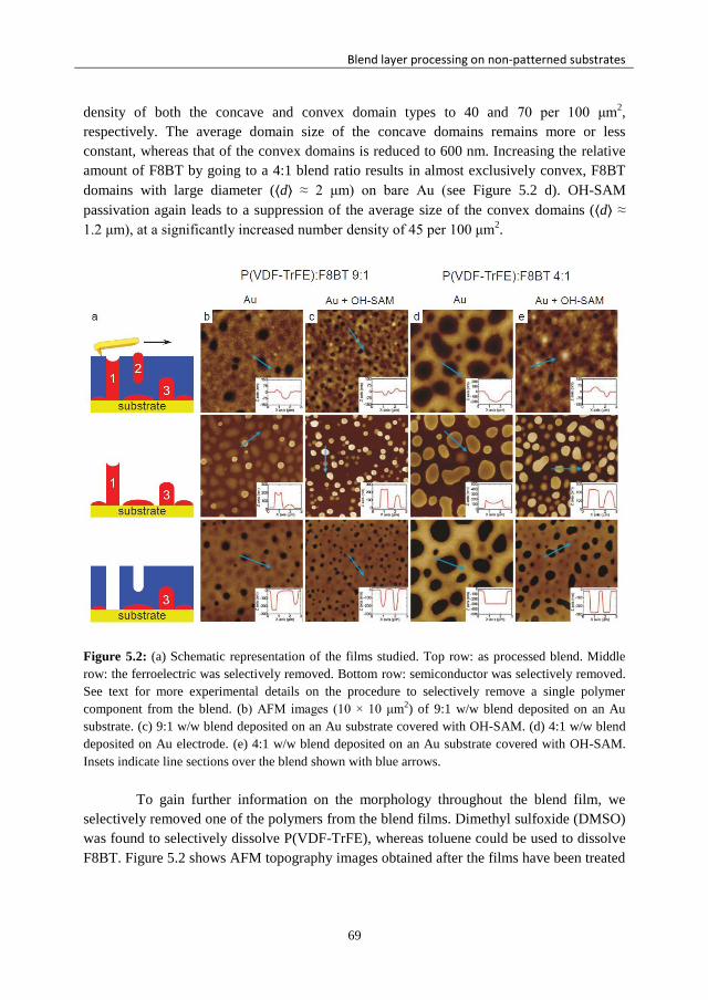
Blend layer processing on non-patterned substrates
69
density of both the concave and convex domain types to 40 and 70 per 100 μm2,
respectively. The average domain size of the concave domains remains more or less
constant, whereas that of the convex domains is reduced to 600 nm. Increasing the relative
amount of F8BT by going to a 4:1 blend ratio results in almost exclusively convex, F8BT
domains with large diameter (⟨d⟩ ≈ 2 μm) on bare Au (see Figure 5.2 d). OH-SAM
passivation again leads to a suppression of the average size of the convex domains (⟨d⟩ ≈
1.2 μm), at a significantly increased number density of 45 per 100 μm2.
Figure 5.2: (a) Schematic representation of the films studied. Top row: as processed blend. Middle
row: the ferroelectric was selectively removed. Bottom row: semiconductor was selectively removed.
See text for more experimental details on the procedure to selectively remove a single polymer
component from the blend. (b) AFM images (10 × 10 μm2) of 9:1 w/w blend deposited on an Au
substrate. (c) 9:1 w/w blend deposited on an Au substrate covered with OH-SAM. (d) 4:1 w/w blend
deposited on Au electrode. (e) 4:1 w/w blend deposited on an Au substrate covered with OH-SAM.
Insets indicate line sections over the blend shown with blue arrows.
To gain further information on the morphology throughout the blend film, we
selectively removed one of the polymers from the blend films. Dimethyl sulfoxide (DMSO)
was found to selectively dissolve P(VDF-TrFE), whereas toluene could be used to dissolve
F8BT. Figure 5.2 shows AFM topography images obtained after the films have been treated
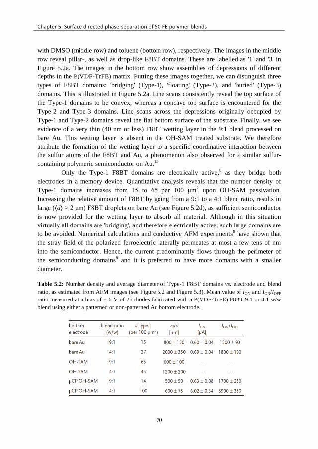
Chapter 5: Surface directed phase-separation of SC-FE polymer blends
70
with DMSO (middle row) and toluene (bottom row), respectively. The images in the middle
row reveal pillar-, as well as drop-like F8BT domains. These are labelled as '1' and '3' in
Figure 5.2a. The images in the bottom row show assemblies of depressions of different
depths in the P(VDF-TrFE) matrix. Putting these images together, we can distinguish three
types of F8BT domains: 'bridging' (Type-1), 'floating' (Type-2), and 'buried' (Type-3)
domains. This is illustrated in Figure 5.2a. Line scans consistently reveal the top surface of
the Type-1 domains to be convex, whereas a concave top surface is encountered for the
Type-2 and Type-3 domains. Line scans across the depressions originally occupied by
Type-1 and Type-2 domains reveal the flat bottom surface of the substrate. Finally, we see
evidence of a very thin (40 nm or less) F8BT wetting layer in the 9:1 blend processed on
bare Au. This wetting layer is absent in the OH-SAM treated substrate. We therefore
attribute the formation of the wetting layer to a specific coordinative interaction between
the sulfur atoms of the F8BT and Au, a phenomenon also observed for a similar sulfur-
containing polymeric semiconductor on Au.15
Only the Type-1 F8BT domains are electrically active,8 as they bridge both
electrodes in a memory device. Quantitative analysis reveals that the number density of
Type-1 domains increases from 15 to 65 per 100 μm2 upon OH-SAM passivation.
Increasing the relative amount of F8BT by going from a 9:1 to a 4:1 blend ratio, results in
large (⟨d⟩ ≈ 2 μm) F8BT droplets on bare Au (see Figure 5.2d), as sufficient semiconductor
is now provided for the wetting layer to absorb all material. Although in this situation
virtually all domains are 'bridging', and therefore electrically active, such large domains are
to be avoided. Numerical calculations and conductive AFM experiments8 have shown that
the stray field of the polarized ferroelectric laterally permeates at most a few tens of nm
into the semiconductor. Hence, the current predominantly flows through the perimeter of
the semiconducting domains8 and it is preferred to have more domains with a smaller
diameter.
Table 5.2: Number density and average diameter of Type-1 F8BT domains vs. electrode and blend
ratio, as estimated from AFM images (see Figure 5.2 and Figure 5.3). Mean value of ION and ION/IOFF
ratio measured at a bias of + 6 V of 25 diodes fabricated with a P(VDF-TrFE):F8BT 9:1 or 4:1 w/w
blend using either a patterned or non-patterned Au bottom electrode.

Blend layer processing on substrates with patterned SAMs
71
Au passivation with OH-SAM leads to suppression of the average size of the Type-1
domains (⟨d⟩ ≈ 1.2 μm), at a number density of 45 per 100 μm2. Nevertheless, some
material remains inactive due to the occurrence of Type-3 features. As for device
performance the number and diameter of the Type-1 F8BT domains are most relevant, we
list these parameters for the different films studied in Table 5.2.
5.2.2 Blend layer processing on substrates with patterned SAMs
It has previously been shown that the domains of a phase-separating mixture of
polymers in a thin film can be guided into periodic structures by a surface with a pre-
patterned variation of surface energies.22,23
This pioneering work focused on the
methodology of this approach rather than incorporating these patterned layers in electronic
devices. Morphology control by surface directed phase separation was explored in organic
light emitting diodes,24–26
photovoltaics27
and thin film transistors.28,29
Next, we show that
this bottom-up approach also works for ferroelectric-semiconductor blends.
Figure 5.3: (a) Schematic representation of the μCP process using a PDMS stamp featuring a
rectangular array of circular posts with a diameter of 0.5 μm and a pitch of 1 μm. b) Schematic
representation of geometrically controlled OH-SAM passivation of the Au substrate. c) AFM image
(10 × 10 μm2) of Au substrate micro-contact printed with OH-SAM. Inset: line scan of the patterned
substrate taken at the position indicated by the blue arrow. (d) Geometrically controlled phase
separation induced by local OH-SAM passivation of the Au substrate. The strong F8BT-Au
interaction is utilized to allow for selective adsorption of the semiconductor onto the Au electrode.

Chapter 5: Surface directed phase- separation of SC-FE polymer blends
72
As mentioned above, F8BT has a coordinative interaction towards Au, which can
be nullified by monolayer passivation of the gold surface. In addition, the calculated
interfacial energies between SAM-passivated gold and the individual blend components
(see Table 5.1), reveal that P(VDF-TrFE) is preferred at an OH-SAM-passivated Au
substrate. These findings can be used to gain better control over the morphology of solution
processed P(VDF-TrFE):F8BT blends. The strong F8BT-Au interaction is utilized to allow
for adsorption of the semiconductor onto designated areas by geometrically controlled OH-
SAM-passivation of the gold substrate prior to casting the P(VDF-TrFE):F8BT blend
solutions (see Figure 5.3). Type-1 F8BT domains are therefore only in physical contact
with bare gold, and possible effects of the OH-SAM changing the workfunction of the gold
electrodes are therefore not relevant in this study.
The OH-SAM is deposited locally using micro-contact printing (μCP).30,31
Figure
5.3a shows a schematic representation of the patterning process of the Au electrode,
together with the dimensions of the features of the PDMS stamp. Figure 5.3b represents a
schematic side view of a μCP Au electrode. OH-SAM is deposited everywhere except for
small circular areas. These circular areas have a nominal diameter of 500 nm and are
periodically placed on a rectangular grid with a periodicity of 1 μm. The molecular
structure of the OH-SAM is also shown. Figure 5.3c shows the AFM topography image of
the patterned Au electrode. The dark circular features in Figure 5.3c correspond to the bare
Au areas, whereas the interstitial area is coated with OH-SAM. The average diameter of the
circular features, as well as the center-to-center distance agree well with the expected
values based on the stamp. Spreading of the OH-SAM ink is limited. The OH-SAM
thickness as determined by AFM is ≈ 2 nm, which is in good agreement with literature
values.32
These results clearly demonstrate that this OH-SAM can be transferred to Au with
excellent pattern replication using μCP.
Figure 5.4 shows AFM topography images of the P(VDF-TrFE):F8BT (9:1 w/w)
and (4:1 w/w) blends spincoated on the Au substrates patterned with OH-SAM, together
with images obtained after selective removal of one of the polymers from the blend films.
Well-ordered 2D arrays of F8BT domains are observed that nicely replicate the μCP
pattern. In fact, pattern replication was achieved over complete cm2-area samples, that is,
much larger length scales than shown in the AFM images in Figure 5.4. Pattern fidelity is
particularly good for the 9:1 w/w blend. However, from the low average height (≈ 100 ‒
150 nm) of the F8BT domains compared to the blend film thickness of 250 nm, we
conclude that about 80 % of the F8BT domains of the patterned 9:1 blend are of non-
bridging Type-3. This assessment is confirmed in the images with the F8BT selectively
removed (bottom row) where only a small number of pits goes all the way down to the
substrate.
Numerical modeling of the phase separation process (see below) predicts that the
number of Type-1 F8BT domains can increase by increasing the relative amount of F8BT.
This is indeed experimentally confirmed by the AFM topography images of the 4:1 (w/w)
Blend layer processing on substrates with patterned SAMs
73
blend (see Figure 5.4b). Almost all F8BT domains have a height that closely matches the
thickness of the as-processed blend film, implying that they are of Type-1. Furthermore, the
average lateral domain size of 0.5 μm at the bottom of the film (lower panel in Figure 5.4b)
is close to the μCP pattern. These results demonstrate that local deposition of OH-SAM by
μCP patterning prior to blend deposition is a simple and powerful technique to influence
the morphology and increase the number of electrically active Type-1 domains.
Figure 5.4: (a) AFM images (10 × 10 μm2) of P(VDF-TrFE):F8BT (9:1 w/w) blend coated on OH-
SAM patterned Au electrode. Top panel: as processed blend. Middle panel: selectively removed
P(VDF-TrFE). Bottom panel: selectively removed F8BT. Insets indicate line sections over the blend
shown with blue arrows. (b) Idem for P(VDF-TrFE):F8BT (4:1 w/w) blend.
Chapter 5: Surface directed phase-separation of SC-FE polymer blends
74
5.2.3 Simulations
Time-resolved numerical modeling of the phase separation process can provide
highly valuable information on the origin of specific features of the phase morphology of
semiconductor/P(VDF-TrFE) mixtures. Fluid phase spinodal decomposition of the
solvent/P(VDF-TrFE)/F8BT ternary under evaporative conditions is modeled by a Cahn-
Hilliard-Cook-deGennes type square gradient approximation. We refer to the Experimental
section for more details regarding the modeling approach. Representation and discussion of
the complete evolution of the microstructure is outside the scope of this chapter. Here we
resort to discussing one (and the same) single time simulation snapshot for both blend
P(VDF-TrFE)/F8BT ratios on patterned and nonpatterned monolayers. The snapshot
represents a transient stage in the coarsening regime which allows the study of critical
features preserved in the dried film.
Figure 5.5 shows simulation results by representing top view, as well as 3D tilted
view images of the phase separated solvent/P(VDF-TrFE):F8BT morphology. The
simulation results for a 9:1 blend ratio reproduce well the regular spacing of the F8BT
domains on the areas without OH-SAM (see Figure 5.4a). The contact line diameter is more
or less equal to the diameter of the dot itself. This seemingly trivial observation suggests
that the spinodal wavelength (which is an intrinsic feature of the blend at a given
composition) is at least of the same order as the dot spacing of the substrate pattern and that
gradient energy contributions are high enough to prevent break-up of transient F8BT-rich
domains into smaller droplets residing on the same dot. In line with the observed
morphology, the numerical model also reproduces that pattern replication of the 9:1 blend
is slightly better than that of the 4:1 blend ratio. Experiments and simulations (see Figure
5.4b and Figure 5.5d) also agree on the somewhat more pronounced lateral scrambling of
the substrate pattern in case of the 4:1 blend, as compared to the 9:1 blend. In contrast,
scrambling of the pattern in the vertical direction is more strongly observed for the 9:1
blend (see Figure 5.4a and Figure 5.5c). The latter observation explains the relatively
abundant occurrence of both Type-2 and Type-3 F8BT domains in the 9:1 blend layers, at
the expense of the desired Type-1 features. Relating to this, the 3D images in Figure 5.5d
clearly show that the features observed at the substrate interface and at the top of the wet
film in most cases belong to the same F8BT-rich domains, suggesting a 4:1 blend ratio to
eventually yield a larger number of Type-1 domains as compared to patterned films
produced from a 9:1 blend. The latter observation is verified by the AFM analysis given in
Figure 5.4.
Interestingly, the simulations suggest that especially in case of the 9:1 blend
F8BT-rich domains can exist that are not in direct contact with either surface (see Figure
5.5a,c). These domains originate from rupture of preceding stratified phase morphology,
induced by surface tension differences between the blend components and/or differences in
the time scales of diffusion and evaporation.33
Merging of these encapsulated F8BT
droplets with Type-2, or Type-3 domains during later stages of drying is expected to

Simulations
75
partially account for the occurrence of Type-1 F8BT domains. They thus form a very
important intermediate state. Direct experimental evidence for the occurrence of these
domains in the actual films is difficult to obtain. Because these domains are fully
encapsulated by the P(VDF-TrFE)-rich matrix, they do not appear in the AFM
measurements of the full blend layer, and they are prone to lift off the substrates upon
selective dissolution of the P(VDF-TrFE) matrix.
Figure 5.5: Numerical simulation of spinodal decomposition of the P(VDF-TrFE):F8BT blend
solution during solvent evaporation on Au electrodes that are (a, b) fully and (c, d) partially covered
with OH-SAM for 9:1 (a, c) and 4:1 (b, d) blend ratios; left panels: overlay of the lateral
concentration fields of P(VDF-TrFE) and F8BT at the substrate (dark: F8BT-rich) and air (bright:
F8BT-rich) interfaces; right panels: tilted 3D top and bottom view images of the phase separated
blend layers: P(VDF-TrFE)-rich (red), F8BT-rich (grey); the same image is shown with a transparent
(top) and solid (bottom) matrix phase.

Chapter 5: Surface directed phase-separation of SC-FE polymer blends
76
5.2.4. Electrical characterization of polymer blend films in ferroelectric
diodes
Memory diodes were made by spincoating a continuous P(VDF-TrFE):F8BT film
on top of i) gold, ii) gold coated with OH-SAM, and iii) gold coated with patterned OH-
SAM. Ba/Al is used as top electrode in all cases. For unclear reasons all (25) memory
diodes made on gold fully covered with OH-SAM were shorted. The typical characteristics
of the memory diodes with bare gold and gold coated with patterned OH-SAM are shown
in Figure 5.6. Ferroelectric polarization reversal occurs at ≈ |10| V, i.e., close to the coercive
electric field of 50 MV/m measured for P(VDF-TrFE) capacitors.34
The polarization is
stable at lower electric fields. Because the perpendicular device current depends on the
direction of the polarization state, this state can be read out repeatedly (non-disturb) at
lower voltages. This forms the basis for these devices as non-volatile, reprogrammable
memories.
Figure 5.6: Current vs. voltage (I-V) hysteretic sweeps of ferroelectric diodes fabricated with a
P(VDF-TrFE):F8BT 9:1 or 4:1 w/w blend using either a patterned or non-patterned Au anode. In all
cases Ba/Al is used as cathode. The diode is swept between + 18.5 and ‒ 18.5 V. Arrows indicate the
scan direction.
As can be seen in Figure 5.6, the average ON-current of the diode with 9:1 w/w
blend and Au electrode (no patterned OH-SAM) is 0.60 ± 0.04 μA at a gate bias of + 6 V.
The average OFF-current (IOFF) is 0.55 ± 0.01 nA. The current modulation ION/IOFF,
therefore, amounts to 1500. This value is already relatively high, and allows integration of
these diodes in 1 kilobit memory arrays.11
IOFF is likely dominated by the leakage currents
caused by nonintrinsic effects like slow depolarization and ionic movement, and seems to
be independent of both the P(VDF-TrFE):F8BT ratio and regularity of the semiconducting
domain pattern. Relative to the 9:1 blend diodes with Au electrodes, 9:1 w/w diodes with

Electrical characterization of polymer blend films in ferroelectric diodes
77
patterned OH-SAM as well as 4:1 w/w diodes with no OH-SAM have a similar value for
ION, and therefore similar ION/IOFF modulation. The ION of the 4:1 w/w diode with patterned
OH-SAM increases nearly one order of magnitude. Table 5.2 shows the mean value of ION
and the ON- to OFF- current ratio (ION/IOFF) measured at a bias of + 6 V over 25 memory
diodes of each type. These results can be correlated to the number density and average size
of electrically active Type-1 F8BT domains. Except for the 4:1 w/w diode with patterned
OH-SAM, the Type-1 F8BT domains have a low density (14 ‒ 27 per 100 μm2).
Furthermore, the semiconductor domain diameter of 4:1 w/w diodes with no OH-SAM of
2000 nm is undesirably large. Therefore, a similar ION is expected in a zero-order
approximation for these diodes. The Type-1 F8BT domain number density in case of the
4:1 w/w diode with patterned OH-SAM reaches an almost maximum number density per
100 μm2. This high density is combined with an average lateral domain size of ≈ 600 nm
because demixing is largely directed by the applied μCP SAM pattern. As a result, a close
to tenfold increase of the ON-current and a sixfold larger current modulation was found in
memory diodes with geometrically controlled phase separation.
Figure 5.7: (a) Data retention: Evolution of current in the ON- state and OFF- state as a function of
time after programming at a bias of + 6 V. (b) Endurance data: Reversible ON- and OFF- switching –
for 1000 consecutive program-erase cycles, readout at + 6 V.
Data retention was examined by programming the device once to the ON- or OFF-
state by applying a + 18.5 and – 18.5 V pulse respectively, and then monitoring the current
over time at + 6 V (see Figure 5.7a). All memory devices show excellent retention. Both
ION and IOFF do not change more than a factor of 3, effectively resulting in a ION/IOFF ratio of
three orders of magnitude after 10 000 s. We see no significant differences in current over
time for the different memories. Because of its higher initial ON-current the 4:1 patterned
devices proved to have the highest ION/IOFF ratio of 1800 after 10 000 s.
In Figure 5.7b the low conductance OFF-state and high conductance ON-state are
measured, while the memory device is repeatedly switching between ON- and OFF- state
by applying program and erase pulses of ± 18.5 V. All memory diodes show reversible

Chapter 5: Surface directed phase-separation of SC-FE polymer blends
78
switching over many cycles. After 1000 cycles an ION/IOFF ratio of over 103 is obtained for
the 4:1 w/w diode with patterned OH-SAM.
5.3 Conclusions
In summary, we have studied in detail the polymer phase separation of P(VDF-
TrFE):F8BT blends. Its morphology is the key to the operation and performance of memory
diodes. Selective dissolution of the individual blend components in combination with AFM
analysis showed that only a limited fraction of the semiconductor domains are electrically
active. In addition, a semi-continuous, thin (< 40 nm) wetting layer of F8BT was found in
case of a reference gold electrode. The specific coordinative interaction between F8BT and
gold has been utilized to allow for adsorption of the semiconductor onto designated areas
by geometrically controlled monolayer passivation of the gold substrate prior to casting of
the P(VDF-TrFE):F8BT blend solutions. Tuning of the P(VDF-TrFE):F8BT blend ratio
resulted in a further optimization of the morphology by maximizing the number of
electrically active semiconducting domains. Thus, size, position and number density of
these domains closely replicated the underlying chemical pattern induced by microcontact
printing.
Full 3D numerical simulation of the surface-controlled demixing process has
provided insight in the ability of the substrate pattern to direct the phase separation, and
hence the regularity of the domain pattern in the final dry blend layers.
The electrical performance of memory diodes could be significantly improved by
blend patterning and composition optimization. A close to tenfold increase of the ON-
current and sixfold larger current modulation was found for memory diodes in which the
number density of electrically active domains was maximized by morphology control.
Hence, the general concept shown here provides a basis to satisfy the demand of improved
functionality and further miniaturization of these memory diodes to smaller feature size
and/or higher integration density.
5.4 Experimental
Poly[(9,9-di-n-octylfluorenyl-2,7-diyl) – alt ‒ (benzo[2,1,3]thiadiazol-4,8-diyl)]
F8BT (Mn = 4.9 kDa, D = 1.8) was synthesized according to a modified Suzuki-
polymerization.35,36
The ferroelectric polymer, poly(vinylidene fluoride-trifluoroethylene)
P(VDF-TrFE) (Mn = 220 kDa, 2.3 < D < 2.8 with a 77/23 VDF/TrFe ratio) was supplied by
Solvay Specialty Polymers. Blend solutions were prepared by co-dissolving P(VDF-TrFE)
and F8BT (9:1 or 4:1 weight ratio) in a mixture of cyclohexanone and tetrahydrofurane
75:25 (v/v) at 50 °C overnight. Cleaned glass substrates with litho patterned gold were
used. Blend films were then spin-coated in a nitrogen-filled glove box. The thickness of the
film was measured with a DEKTAK profilometer and varied between 200 ‒ 230 nm.

Experimental
79
Subsequently, the samples were annealed at 135 °C for 5 min. Finally, the Ba/Al cathode is
evaporated through a shadow mask, followed by thin film encapsulation. Surface
topography of the dried blend films was examined by atomic force microscopy.
Topography is measured using a sharp (apex radius < 10 nm) AFM tip in tapping-mode
(TM). The AFM measurements were performed using Al coated Si tips (Nanosensors,
spring constant k ≈ 12.5 N/m).
Contact angle measurements were performed at room temperature (22 °C) on an
Easydrop Standard (Krüss) goniometer using a drop size of 2 μL. Surface-directed phase
separation of semiconductor ferroelectric polymer blend films using the microcontact
printing technique was performed on patterned UV-ozone cleaned gold electrodes. A h-
poly(dimethylsiloxane) PDMS stamp, featuring a 2D pillar grid of 475 ‒ 565 nm wide dots
with 1000 nm ± 3% pitch, was used. Stamps were inked by immersing them in 11-
mercapto-1-undecanol solution (1 mM in ethanol) for about 10 min. After removal from the
ink solutions, all stamps were rinsed with ethanol and dried in a stream of nitrogen for
about 30 s. Stamping was performed manually for 20 s by using tweezers for stamp
handling and by taking advantage of the natural stamp-substrate adhesion. No extra
pressure was applied. A blend of P(VDF-TrFE):F8BT (9:1 or 4:1 weight ratio) in a mixture
of cyclohexanone and tetrahydrofurane 75:25 (v/v) was then spin-coated in a nitrogen-filled
glove box onto this patterned surface at 2500 rpm for 60 s and subsequently annealed for 5
min at 135 °C.
Fluid phase spinodal de-mixing of the solvent/P(VDF-TrFE)/F8BT blend under
evaporative conditions is modeled by a Cahn-Hilliard-Cook-deGennes type square gradient
approximation,37–39
involving a ternary Flory-Huggins local mixing free energy.40,41
The
usual bulk free energy functional comprising local and non-local contributions is
augmented with terms describing the interaction between the blend components and the
substrate- and air interfaces as effective interaction parameters42
adopting non-zero values
only at, respectively, z = 0 and z = h. Solvent evaporation is treated according to a
previously published procedure,43
which at each time step calculates an instantaneous
global evaporation rate based on a (relative) mass transfer coefficient and the mean volume
fraction of solvent in the top of the fluid layer. The mass loss due to evaporation is then
compensated for by downscaling the grid spacing in the z-dimension.44
The model does not
take the final stages of drying into account. The input parameters for the simulations are
summarized by the tables shown in the supplementary info. Table 5.3 lists the Flory-
Huggins parameters (i.e., effective degree of polymerization Ni and mutual interaction
parameter χij), whereas Table 5.4 gives the air and substrate interaction parameters. The
effective degrees of polymerization are obtained by scaling the average molar volume of
the polymers to that of the solvent (cyclohexanone). Solvent-polymer interaction
parameters χlj are chosen to comply with the constraint of compatibility with both polymers
(χ1j < 0.5), whereby it is assumed that P(VDF-TrFE) is somewhat better soluble than F8BT
(χ13 < χ12). Polymer-polymer interaction parameter χ23 is taken sufficiently high so as to
avoid the formation of mixed binodal phases, that is, in agreement with experimental

Chapter 5: Surface directed phase-separation of SC-FE polymer blends
80
findings.13
Surface interaction parameters χia and χi
s are quantified via the method explained
in another study42
involving the measured disperse (γd) and polar (γ
p) surface energy
contributions of the blend components and the substrate (see Table 5.1). As mentioned, the
coordinative interaction between F8BT and Au cannot be defined by the method of surface
energy measurement. Instead, a highly negative (attractive) value of χ2s = – 200 is assumed
to model the coordination. The choice of this number is admittedly arbitrary, but its exact
value is not influencing the outcome of the simulations on a qualitative level.
Table 5.3: Flory-Huggins parameters (effective degree of polymerization and interaction parameters)
for the ternary blend solvent/F8BT/P(VDF-TrFE)
Table 5.4: Substrate and air-interaction parameters for the ternary blend solvent/F8BT/P(VDF-TrFE)
The data in Table 5.4 allows computational reproduction of the experimental dot-
pattern in the Au substrate passivation by the microcontact printed OH-SAM by assigning
the χsi-Au and χ
si-OH parameters for each blend component to specified clusters of elements
on a periodic 2D grid which functions as the substrate in the 3D simulations. 100- or 25-
fold replication of the single-dot unit cell in a square geometry is respectively implemented
on a 150 × 150 or 75 × 75 grid. At the air interface the surface tension for each pure
component is represented isotropically by χa .
42

References
81
5.5 References
[1] J. Smith, R. Hamilton, I. McCulloch, N. Stingelin-Stutzmann, M. Heeney, D.D.C. Bradley,
T.D. Anthopoulos, Solution-processed organic transistors based on semiconducting blends,
J. Mater. Chem. 2010, 20, 2562, and references cited therein.
[2] C.J. Brabec, M. Heeney, I. McCulloch, J. Nelson, Influence of blend microstructure on bulk
heterojunction organic photovoltaic performance, Chem. Soc. Rev. 2011, 40, 1185.
[3] A.C. Morteani, A.S. Dhoot, J.S. Kim, C. Silva, N.C. Greenham, C. Murphy, E. Moons, S.
Ciná , J.H. Burroughes, R.H. Friend, Barrier-free electron–hole capture in polymer blend
heterojunction light-emitting diodes, Adv. Mater. 2003, 15, 1708.
[4] A.C. Arias, F. Endicott, R.A. Street, Surface-induced self-encapsulation of polymer thin-
film transistors, Adv. Mater. 2006, 18, 2900.
[5] K. Asadi, D.M. de Leeuw, B. de Boer, P.W.M. Blom, Organic non-volatile memories from
ferroelectric phase-separated blends, Nature Mater. 2008, 7, 547.
[6] Polymer Blends Handbook, (Ed: L. A. Utracki), Kluwer Academic Publishers, Dordecht
2002.
[7] M. Kemerink, K. Asadi, P.W.M. Blom, D.M. de Leeuw, The operational mechanism of
ferroelectric-driven organic resistive switches, Org. Electronics 2012, 13, 147.
[8] V. Khikhlovskyi, R. Wang, A.J.J.M. van Breemen, G.H. Gelinck, R.A.J. Janssen, M.
Kemerink, Nanoscale organic ferroelectric resistive switches, J. Phys. Chem. C 2014, 11,
3305.
[9] K. Asadi, H.J. Wondergem, R.S. Moghaddam, C.R. McNeill, N. Stingelin, B. Noheda,
P.W.M. Blom, D.M. de Leeuw, Spinodal decomposition of blends of semiconducting and
ferroelectric polymers, Adv. Funct. Mater. 2011, 21, 1887.
[10] M. Li, N. Stingelin, J.J. Michels, M.-J. Spijkman, K. Asadi, R. Beerends, F. Biscarini,
P.W.M. Blom, D.M. de Leeuw, Processing and low voltage switching of organic
ferroelectric phase-separated bistable diodes, Adv. Funct. Mater. 2012, 22, 2750.
[11] A.J.J.M. van Breemen, J.-L. van der Steen, G. van Heck, R. Wang, V. Khikhlovskyi, M.
Kemerink, G.H. Gelinck, Crossbar arrays of nonvolatile, rewritable polymer ferroelectric
diode memories on plastic substrates, Appl. Phys. Expr. 2014, 7, 031602.
[12] M.A. Khan, U.S. Bhansali, D. Cha, H.N. Alshareef, All-polymer bistable resistive memory
device based on nanoscale phase-separated PCBM-ferroelectric blends, Adv. Funct. Mater.
2013, 23, 2145.
[13] J.J. Michels, A.J.J.M. van Breemen, K. Usman, G.H. Gelinck, Liquid phase demixing in
ferroelectric/semiconducting polymer blends: an experimental and theoretical study, J.
Polymer. Sci. Part B: Polymer. Phys. 2011, 49, 1255.
[14] S.Y. Heriot, R.A.L. Jones, An interfacial instability in a transient wetting layer leads to
lateral phase separation in thin spin-cast polymer-blend films, Nat. Mater. 2005, 4, 782.
[15] C.M. Björström, S. Nilsson, A. Bernasik, A. Budkowski, M. Andersson, K.O. Magnusson,
E. Moons, Vertical phase separation in spin-coated films of a low bandgap
polyfluorene/PCBM blend‒effects of specific substrate interaction, Appl. Surf. Sci. 2007,
253, 3906.
[16] R. Hamilton, J. Smith, S. Ogier, M. Heeney, J.E. Anthony, I. McCullogh, J. Veres, D.D.C.
Bradley, T.D. Anthopoulos, High-performance polymer-small molecule blend organic
transistors, Adv. Mater. 2009, 21, 1166.

Chapter 5: Surface directed phase-separation of SC-FE polymer blends
82
[17] A. Bernasik, J. Wlodarczyk-Miskiewicz, W. Luzny, K. Kowalski, J. Raczkowska, J. Rysz,
A. Budkowski, Lamellar structures formed in spin-cast blends of insulating and conducting
polymers, Synth. Met. 2004, 144, 253.
[18] T. Fukuma, K. Kobayashi, T. Horiuchi, H. Yamada, K. Matsushige, Nanometer-scale
characterization of ferroelectric polymer thin films by variable-temperature atomic force
microscopy, Jap. J. Appl. Phys. 2000, 39, 3830.
[19] D.K. Owens, R.C. Wendt, Estimation of the surface free energy of polymers, J. Appl.
Polym. Sci. 1969, 13, 1741.
[20] D.Y. Kwok, A.W. Neumann, Contact angle measurement and contact angle interpretation,
Adv. Colloid Interface Sci. 1999, 81, 167.
[21] F.M. Fowkes, Attractive forces at interfaces, Ind. Eng. Chem. 1964, 56, 40.
[22] M. Böltau, S. Walheim, J. Mlynek, G. Krausch, U. Steiner, Surface-induced structure
formation of polymer blends on patterned substrates, Nature 1998, 391, 877.
[23] K.-H. Yim, Z. Zheng, R.H. Friend, W.T.S. Huck, J.-S. Kim, Surface-directed phase
separation of conjugated polymer blends for efficient light-emitting diodes, Adv. Funct.
Mater. 2008, 18, 2897.
[24] A. Budkowski, A. Bernasik, P. Cyganik, J. Rysz, R. Brenn, Surface-directed phase
separation in nanometer polymer films: self-stratification and pattern replication, e-Polym.
2013, 2, 88.
[25] G. Fichet, N. Corcoran, P.K.H. Ho, A.C. Arias, J.D. Mackenzie, W.T.S. Huck, R.H. Friend,
Self-organized photonic structures in polymer light-emitting diodes, Adv. Mater. 2004, 16,
1908.
[26] N. Corcoran, P.K.H. Ho, A.C. Arias, J.D. Mackenzie, R.H. Friend, G. Fichet, W.T.S. Huck,
Highly-efficient broadband waveguide outcoupling in light-emitting diodes with self-
organized polymer blends, Appl. Phys. Lett. 2004, 85, 2965.
[27] L.-M. Chen, Z. Xu, Z. Honga, Y. Yanga, Interface investigation and engineering –
achieving high performance polymer photovoltaic devices, J. Mater. Chem. 2010, 20, 2575.
[28] X. Wang, W.H. Lee, G. Zhang, X. Wang, B. Kang, H. Lu, L. Qiu, K. Cho, Self-stratified
semiconductor/dielectric polymer blends: vertical phase separation for facile fabrication of
organic transistors, J. Mater. Chem. C 2013, 1, 3989.
[29] C. Liu, Y. Li, M.V. Lee, A. Kumatania, K. Tsukagoshi, Self-assembly of
semiconductor/insulator interfaces in one-step spin-coating: a versatile approach for organic
field-effect transistors, Phys. Chem. Chem. Phys. 2013, 15, 7917.
[30] J.L. Wilbur, A. Kumar, H.A. Biebuyck, E. Kim, G.M. Whitesides, Microcontact printing of
self-assembled monolayers: applications in microfabrication, Nanotechnology 1996, 7, 452.
[31] A. Perl, D.N. Reinhoudt, J. Huskens, Microcontact printing: limitations and achievements,
Adv. Mater. 2009, 21, 2257.
[32] C.D. Bain, E.B. Troughton, Y.-T. Tou, J. Evall, G.M. Whitesides, R.G. Nuzzo, Formation
of monolayer films by the spontaneous assembly of organic thiols from solution onto gold,
J. Am. Chem. Soc. 1989, 111, 321.
[33] O. Wodo, B. Ganapathysubramanian, Modeling morphology evolution during solvent-based
fabrication of organic solar cells, Comput. Mater. Sci. 2012, 55, 113.
[34] T. Furukawa, Ferroelectric properties of vinylidene fluoride copolymers, Phase Trans.
1989, 18, 143.
References
83
[35] T. van Woudenbergh, J. Wildeman, P.W.M. Blom, J.J.A.M. Bastiaansen, B.M.W.
Langeveld-Voss, Electron-enhanced hole injection in blue polyfluorene-based polymer
light-emitting diodes, Adv. Funct. Mater. 2004, 14, 677.
[36] N. Miyaura, A. Suzuki, Palladium-catalyzed cross-coupling reactions of organoboron
compounds, Chem. Rev. 1995, 96, 2457.
[37] J.W. Cahn, J.E. Hilliard, Free energy of a nonuniform system. I. Interfacial free energy, J.
Chem. Phys. 1958, 28, 258.
[38] H.E. Cook, Brownian motion in spinodal decomposition, Acta Metall. 1970, 17, 297.
[39] P.G. de Gennes, Scaling concepts in polymer physics, Cornell University Press, Ithaca, NY
1979.
[40] P.J. Flory, Principles of polymer chemistry, Cornell University Press, Ithaca, NY 1953.
[41] The simulations involve a single solvent rather than a mixture to allow for reasonable
computation times. The effect of an actual binary solvent system is outside the scope of this
paper.
[42] J.J. Michels, E. Moons, Simulation of surface-directed phase separation in a solution-
processed polymer/PCBM blend, Macromolecules 2013, 46, 8693.
[43] C.-S. Kim, D.M. Saylor, M.K. McDermott, D.V. Patwardhan, J.A. Warren, Modeling
solvent evaporation during the manufacture of controlled drug-release coatings and the
impact on release kinetics, J. Biomed. Mater. Res. Part B: Appl. Biomater. 2009, 688.
[44] G.A. Buxton, N. Clarke, Ordering polymer blend morphologies via solvent evaporation,
Eur. Polym. Lett. 2007, 78, 56006.

Chapter 5: Surface directed phase-separation of SC-FE polymer blends
84

85
Chapter 6
Detailed study of the wetting layer and its influence
on the performance of the ferroelectric diode
It has become evident from Chapter 5 that the same materials can exhibit a wide
range of performances depending on variations in the phase-separated morphology of the
blend, induced by, amongst others, different processing conditions. In this chapter, as
natural next step, we aim at understanding the structure of the wetting layer, described in
Chapters 4 and 5, and its influence on the device performance. A combination of AFM,
PFM and selective dissolution was used. We show that the wetting layer makes it
impossible to fully pole the ferroelectric in the reverse direction. We propose an optimal
and simple fabrication recipe to avoid the formation of the wetting layer and to provide an
improved blend structure. Finally, it was found experimentally that the devices without
wetting layer demonstrate much better endurance characteristics.

Chapter 6: Detailed study of the wetting layer in the ferroelectric diode
86
6.1 Introduction
It has become evident from Chapter 5 that the same materials can exhibit a wide
range of performances depending on variations in the phase-separated morphology of the
blend, induced by, amongst others, different processing conditions.1 In Chapter 4 and 5 the
full 3D structure of the blend was reconstructed: three types of domains and a wetting layer
on the substrate were found in the blend. In Chapter 3 it was shown that the ferroelectric
polarization is crucial for the modulation of the injection barrier in the device. However, the
presence of the wetting layer might influence the switching properties of the blend2-4
and
therefore harm the device performance.
In this chapter, as natural next step, we aim at understanding the structure of the
wetting layer and its influence on the device performance. We use a combination of atomic
force microscopy (AFM) and piezoresponse force microscopy (PFM) to probe the
topography of the wetting layer, study its influence on the ferroelectric properties of the
blend and hence the device performance. We proposed an optimal and simple fabrication
recipe that provides an improved blend structure which does not suffer from the wetting
layer. It was found experimentally that the devices without wetting layer demonstrate much
better endurance characteristics.
6.2 Results and discussion
6.2.1 Detailed study of the wetting layer
Detailed study of the wetting layer is essential for understanding its influence on
the device performance. Similar to Chapter 4 and 5, the selective dissolution technique was
used to reveal the 3D structure and hence the wetting layer of the blend deposited on two
different substrates: Au and Mo/MoOx. Figures 6.1a,b show topography images of the
blend deposited on Au and Mo/MoOx substrates respectively, obtained by selective
dissolution of the ferroelectric component. Both images show a 'forest' of vertical
semiconducting domains. However, a remarkable feature in Figure 6.1a is the wetting
layer, in our case apparent as a large number of wide semiconducting islands with a height
of around 30 nm which is significantly lower than the average thickness of the blend. The
presence of the wetting layer leads to a smaller number of electrically active domains
(Type-1, see Chapters 3 and Chepter 4). In contrast, the blend deposited on Mo/MoOx
substrate in Figure 6.1b does not show any wetting layer, which is most likely explained by
the modified surface energy of the substrate (see Chapter 5).1

Detailed study of the wetting layer
87
Figure 6.1: AFM topography images (10 × 10 µm2) of a P(VDF-TrFE):F8BT (9:1 w/w) blend with
selectively dissolved P(VDF-TrFE) phase: (a) Deposited on Au. Three arbitrarily chosen islands
corresponding to the wetting layer are shown with red dashed circles. (b) Deposited on Mo/MoOx
substrates. Total vertical scale ‒ 500 nm.
It has already been shown in Chapter 3 that the ferroelectric polarization is crucial
for the modulation of the injection barrier in the device. Hence the correlation between the
wetting layer and the corresponding ferroelectric properties of the blend at the local scale
was investigated. Figure 6.2 presents topography (a, c) and piezoresponse (b, d) of the
blend deposited on Au under various polarization conditions. In order to emphasize the
effect of the poling, a smaller area of (8 × 8 µm2) concentric with the (10 × 10 µm
2) image
was negatively polarized (upward polarization, oriented from the bottom contact to the
surface of the blend) and positively (downward) polarized by applying – 20 V and + 20 V
to the tip, respectively. Note that poling needs to apply a voltage between the sample and
the tip that is above the coercive voltage of the ferroelectric film, i.e. in this case ≈ |10| V
(see Chapter 2).5 The AFM tip is then scanned in contact mode over the desired area. In the
case of negative poling, the comparison between the topography in panel a and the PFM
amplitude in panel b shows that, as expected, the piezoresponse comes only from the
ferroelectric matrix phase of the blend, and not from the semiconducting phase. All
semiconductor domains appear in the piezoresponse image as dark spots, corresponding to
zero piezoresponse. In case of a positive poling voltage, panels c and d, the PFM signal
reveals to be significantly inhomogeneous with pronounced 'blind' islands, i.e. regions that
give zero PFM signal. Comparison between Figure 6.1a and Figure 6.2d suggests that such
islands most likely correspond to regions under which a wetting layer is buried: the pattern
of the islands in the selective dissolved topography image of the same blend, shown in
Figure 6.1a, matches the pattern of the unpoled regions in Figure 6.2d. And interestingly,
most of the protruding domains partially or fully coincide with the islands as shown in
Figure 6.3. This is in a good agreement with selective dissolved topography image of the
same blend shown in Figure 6.1a in which the network of the islands matches the structure
of the wetting layer.

Chapter 6: Detailed study of the wetting layer in the ferroelectric diode
88
Figure 6.2: PFM‒images (10 × 10 µm2) of a P(VDF-TrFE):F8BT blend deposited on Au electrode,
with from left to right: (a) The topography, (b) The piezoforce amplitude in the case of negative
polarization (upwards), and (c), (d) respectively for positive polarization (downwards). Note that the
poling was performed on 8 × 8 µm2 concentric areas to emphasize its effect. Selected full and floating
domains are marked with white circles and squares respectively.
The network of the blind islands in Figure 6.2d originates from the fact that the
ferroelectric material requires a sufficient number of compensation charges in the contacts
in order to pole and stabilize its polarization state.2-4
Figure 6.4 gives a detailed explanation
of the observed phenomenon by showing a schematic representation of the voltage
distribution with and without the wetting layer. The ferroelectric and semiconductor layers
act as two capacitors in series. In case the semiconductor provides a sufficient number of
compensation charges it effectively becomes part of the contact. This means that the full
applied voltage drops over the ferroelectric layer which therefore can be poled, as shown in
Figure 6.4a. Hence the PFM signal in the FE-phase in Figure 6.2b is homogeneous. In
contrast, if the semiconductor does not provide enough compensation charges it acts
together with the ferroelectric layer as a voltage divider. Hence the voltage drops mostly
over the layer with lowest dielectric constant, i.e. the semiconductor and the ferroelectric

Detailed study of the wetting layer
89
cannot be poled as described in Figure 6.4b. Hence the absence of the PFM signal on such
islands is due to the fact that the semiconductor polymer F8BT is a poor electron
transporter.6 This makes it impossible to pole and stabilize the ferroelectric polarization for
positive applied tip voltages at places where semiconductor material is located at the
bottom electrode.
Figure 6.3: AFM topography image (10 × 10 µm2) of a P(VDF-TrFE):F8BT blend deposited on a Au
electrode (see Figure 6.2c). Red circles correspond to the completed semiconducting domains
whereas dark contours represent the boundaries of the islands corresponding to the wetting layer of
the blend revealed by PFM (see Figure 6.2d).
Figure 6.4: Schematic representation of the ferroelectric polarization in a M/FE/SC/M structure. (a)
Ferroelectric polarization is preserved and stabilized by holes in the p-type semiconductor. (b)
Ferroelectric polarization is absent as the p-type semiconductor cannot provide electrons. Graphs
below the figures sketch the voltage distribution in the corresponding devices.

Chapter 6: Detailed study of the wetting layer in the ferroelectric diode
90
This finding is further supported by a similar measurement set on blend layers
deposited on a Mo/MoOx substrate, shown in Figure 6.5a‒d. As compared to Figure 6.1b, a
first observation is that the semiconducting domains have in average a significantly smaller
diameter, but their density is larger. Second, the measured piezoresponse of the ferroelectric
phase for positive applied voltage (see panel d) is way more homogeneous and comparable
to that of the negatively poled situation (see panel b). This is consistent with the
morphology of the blend revealed in Figure 6.1b. The most important observation is that
the morphology of the blend deposited on Mo/MoOx substrate demonstrates a similar
morphology to the blend deposited on Au substrates covered with an OH-terminated SAM
(see Figure 5.2, Chapter 5).1 However, the fabrication recipe for the Mo/MoOx ‒ based
device is much better in terms of the reproducibility and simplicity since it does not require
a preparation of the solution and an overnight deposition (complexity) of the full-coverage
(reproducibility) OH-terminated SAM.
Figure 6.5: PFM‒images (10 × 10 µm2) of a P(VDF-TrFE):F8BT blend deposited on a Mo/MoOx
electrode, with from left to right: the topography (a), the piezoresponse amplitude (b), in the case of
negative polarization (upwards), and (c), (d) the same for positive polarization (downwards). Again
the poling was performed on 8 × 8 µm2 concentric areas to emphasize its effect.

Detailed study of the wetting layer
91
A next step was to check the performance of the Mo/MoOx – based devices and
compare them with the Au ‒ based devices. Figure 6.6a,b shows the endurance data of the
Mo/MoOx/P(VDF-TrFE):F8BT/Ba/Al and Au/P(VDF-TrFE):F8BT/Ba/Al devices
respectively. Both graphs describe the evolution of the I-V characteristics upon consecutive
program-erase cycles. Despite the fact that Mo/MoOx ‒ based device has no wetting layer at
the bottom electrode, it does not show significantly higher currents in the (positive) forward
direction than the Au-based device, similar to the OH-terminated SAM devices (see Figure
5.6, Chapter 5). In fact, this lack of difference is not surprising: at forward bias, the bottom
contact is positive, which means that an eventual wetting layer has to provide holes to
enable poling the ferroelectric matrix, which is no problem for the p-type semiconductor
used.
In view of the above, the effect of the absence or presence of the wetting layer on
the I-V characteristics of the blend would likely be more clearly reflected on devices with
symmetric electrodes. However, the effect can also be seen for the current, asymmetric
devices. This is visible in Figure 6.6 where the Mo/MoOx/P(VDF-TrFE):F8BT/Ba/Al-
device provides an (undesirable) higher current at reverse bias as compared to the
Au/P(VDF-TrFE):F8BT/Ba/Al-device because of the presence of the wetting layer, which
hampers the charge injection in the device, in the latter case.
Finally, from Figure 6.6, it turned out that the Mo/MoOx ‒ based device
demonstrates much better endurance characteristics than the Au – based one. The reason for
this is unclear at present, nor is it evident that this is related to the absence of a wetting
layer. Hence using Mo/MoOx as the bottom electrode provides an easier fabrication recipe,
higher reproducibility and improved endurance characteristics.
Figure 6.6: Endurance data: Reversible ON- and OFF- switching of the devices: (a)
Mo/MoOx/P(VDF-TrFE):F8BT/Ba/Al (b) Au/P(VDF-TrFE):F8BT/Ba/Al. Black, red, blue and purple
curves correspond to 1, 10, 100 and 1000 consecutive program-erase cycles respectively.

Chapter 6: Detailed study of the wetting layer in the ferroelectric diode
92
6.3 Conclusions
In summary, we have studied the structure of the wetting layer and its influence on
the device performance. We used a combination of atomic force microscopy (AFM) and
piezoresponse force microscopy (PFM) to probe the topography of the wetting layer, study
its influence on the polarizibility of the blend and hence the device performance. We
showed that the wetting layer makes it impossible to pole large parts of the device in the
reverse direction. We proposed an optimal and simple fabrication recipe, making it possible
to improve blend structure preventing suffering from the wetting layer. Finally, it was
found experimentally that the devices without wetting layer demonstrate much better
endurance characteristics.
6.4 Experimental
Poly(vinylidene fluoride-trifluoroethylene) P(VDF-TrFE) (Mn = 220 kDa, 2.3 < D
< 2.8 with a 77/23 VDF/TrFe ratio) was supplied by Solvay Specialty Polymers. Poly[(9,9-
di-n-octylfluorenyl-2,7-diyl)-alt-(benzo[2,1,3]thiadiazol-4,8-diyl)] F8BT (Mn = 13 kDa, D
= 2.0) was synthesized according to a modified Suzuki-polymerization.7,8
The active layer in this work is formed by a continuous film of a 1:9 wt/wt blend
of F8BT and P(VDF-TrFE). The blend film was spin-coated on top of glass substrates with
patterned bare Au and Mo/MoOx (thin layer of ≈ 1 nm of MoOx was deposited on Mo
substrate) electrodes and subsequently annealed at 135 °C for 1 h to enhance the
crystallinity of the ferroelectric phase. Using surface profilometry we determined the layer
thickness of the P(VDF-TrFE):F8BT blend to be ≈ 200 ± 10 nm.
In order to reconstruct the 3D structure of the self-assembled blend, selective
chemical dissolutions of both polymers were performed. Dimethyl sulfoxide (DMSO) was
used to dissolve the ferroelectric P(VDF-TrFE) and toluene for the semiconductor (F8BT)
parts of the blend.
Atomic force microscopy (AFM) and piezoresponse force microscopy (PFM) were
employed to locally probe topography and polarization states respectively. Standard PFM
measurements were performed using a high-resolution MFM from the company NanoScan
(Switzerland), in contact mode and operated in air, at room temperature. An additional
lock-in amplifier (Zürich Instruments, Switzerland) was used to feedback and measure the
PFM signal.

References
93
6.5 References
[1] A.J.J.M. van Breemen, T. Zaba, V. Khikhlovskyi, J. Michels, R.A.J. Janssen, M. Kemerink,
G.H. Gelinck, Surface directed phase separation of semiconductor ferroelectric polymer
blends and their use in non-volatile memories, Adv. Funct. Mater. 2015, 25, 278.
[2] I.P. Batra, P. Wurfel, B.D. Silverman, Phase-transition, stability and depolarization
ferroelectric thin-films, Phys. Rev. B 1973, 8, 7, 3257.
[3] P. Wurfel, I.P. Batra, J.T. Jacobs, Polarization instability in thin ferroelectric films, Phys.
Rev. Lett. 1973, 30, 1218.
[4] P. Wurfel, I.P. Batra, Depolarization-field-induced instability in thin ferroelectric films ‒
experiment and theory, Phys. Rev. B 1973, 8, 5126.
[5] V. Khikhlovskyi, A.V. Gorbunov, A.J.J.M. van Breemen, R.A.J. Janssen, G.H. Gelinck, M.
Kemerink, Multi-bit organic ferroelectric memory, Org. Electron. 2013, 14, 3399.
[6] Y. Zhang, P.W.M. Blom, Electron and hole transport in poly(fluorene-benzothiadiazole),
Appl. Phys. Lett. 2011, 98, 143504.
[7] T. van Woudenbergh, J. Wildeman, P.W.M. Blom, J.J.A.M. Bastiaansen, B.M.W.
Langeveld-Voss, Electron-enhanced hole injection in blue polyfluorene-based polymer
light-emitting diodes. Adv. Funct. Mater. 2004, 14, 677.
[8] N. Miyaura, A. Suzuki, Palladium-catalyzed cross-coupling reactions of organoboron
compounds, Chem. Rev. 1995, 95, 2457.

Chapter 6: Detailed study of the wetting layer in the ferroelectric diode
94

95
Chapter 7
Data retention in ferroelectric diodes
Solution-processed ferroelectric diodes could become the long-missing non-
volatile memory elements in organic electronic devices. To this end, data retention in these
devices should be characterized, understood and controlled. First, we show that the
measurement protocol can strongly affect the 'apparent' retention time and we identify a
suitable protocol. Second, we show by experimental and theoretical methods that partial
depolarization of the ferroelectric is the major mechanism responsible for imperfect data
retention. This depolarization occurs in close vicinity to the semiconductor-ferroelectric
interface, is driven by energy minimization and is inherently present in this type of phase-
separated polymer blends. Third, we experimentally and numerically demonstrate a direct
relation between data retention and the charge injection barrier height of the diode. Tuning
the injection barrier height allows to improve retention by many orders of magnitude in
time, albeit at the cost of a reduced on/off ratio.
Based on:
V. Khikhlovskyi, A.J.J.M. van Breemen, R.A.J. Janssen, G.H. Gelinck, M. Kemerink, Data retention
in organic ferroelectric resistive switches.
Chapter 7: Data retention in ferroelectric diodes
96
7.1 Introduction
There is an evident demand for non-volatile memory elements in organic
electronics. Unlike in e.g. the silicon industry, in organic electronics there does to date not
exist a technology that fulfils all demands for a non-volatile memory.1,2
Solution-processed
ferroelectric diodes have recently been proposed as a very promising practical realization of
a non-volatile memory that can be read out non-destructively and is compatible with
flexible electronics and large area applications.3,4
The ferroelectric diode consists of a thin
film made of a polymeric semiconductor-ferroelectric blend sandwiched between two
electrodes. The phase separation in the blend is driven by a spinodal decomposition process
which results in sub-micron sized semiconductor domains embedded in a ferroelectric
matrix. Thus, transport of charge carriers, which is needed for the resistive read out, is
possible only via the semiconducting phase. The working principle of the ferroelectric
diode relies on a modulation of the barrier for charge injection from the metal electrode into
the semiconductor by the polarization charges in the ferroelectric.5,6
This makes it possible
to switch the device between high- and low- resistive states. The non-volatility and
bistability of the ferroelectric diode stem from the remnant polarization of the ferroelectric
part of the blend.
Data retention is a crucial parameter for memory elements. It is known that the
depolarization phenomenon that occurs in the ferroelectric is the major factor that harms the
device performance.7 However, the detailed mechanism of information loss, especially at
the local scale, is unknown. Moreover, although there are a number of publications in
which data retention of ferroelectric diodes is studied,8-10
the exact measurement scheme
was not always specified. This hampers both comparison between reports and the
assessment of the actual relevance for applications.
In this chapter, we address the related questions regarding the importance of a
well-chosen measurement protocol, the mechanism of the information loss, and ways to
mitigate data retention. We show that the data retention is intimately linked to the
morphology of the phase-separated polymer blend and is due to polarization loss in a
narrow region around the semiconducting domains. From theoretical considerations we
show that the polarization in this region is inherently instable. As such, the mechanism
governing retention in our devices is fundamentally different from those in ferroelectric-
only devices11,12
and in semiconductor-ferroelectric-metal multilayers.13,14
Mitigation of this
fundamental problem is however possible. We find a direct relation between data retention
and the charge injection barrier height of the ferroelectric diode which allows to improve
retention by many orders of magnitude in time, albeit at the cost of a reduced on/off ratio.

Electrical and memory characteristics of a ferroelectric diode
97
7.2 Results and discussion
7.2.1 Electrical and memory characteristics of a ferroelectric diode
Figure 7.1a shows the hysteretic current-voltage (I-V) curve measured on the
device fabricated with a P(VDF-TrFE):F8BT 9:1 blend. A Au/MoOx bottom electrode was
chosen for hole injection. The work-function of Au/MoOx electrode is estimated to be ≈ 5.0
eV15
because a very thin layer of MoOx (~ 1 nm) was deposited. Since the energy level of
the highest occupied molecular orbital (HOMO) of F8BT amounts to 5.9 eV vs. vacuum,
the hole injection barrier from Au/MoOx to HOMO of F8BT is of the order of 1 eV. The
contribution from electron transport to the total current, provided by the top Ba/Al
electrode, is thought to be negligible because of the low electron mobility in F8BT.16
However the top Ba/Al electrode is essential for providing asymmetric I-V characteristics
of the device. Without ferroelectric polarization the large charge injection barrier limits
hole injection and, therefore, the current in the device is low. However, the injection barrier
can be tuned with the assistance of the stray field of the ferroelectric polarization charges.5,6
The ascending curve in Figure 7.1a shows that upon increasing the applied voltage the
ferroelectric becomes polarized which consequently lowers the injection barrier, leading to
a significant current increase which occurs at around the coercive voltage of + 10 V.17
As
the ferroelectric preserves its polarization state when the applied voltage is turned off, the
descending part of the I-V curve does not follow the ascending one. Thus the positive part
of the I-V sweep demonstrates significant hysteresis behavior and the device can be
Figure 7.1: Electrical and memory characteristics of a ferroelectric diode fabricated based on a
P(VDF-TrFE):F8BT 9:1 blend with Au/MoOx bottom and Ba/Al top electrodes. (a) Hysteretic
current-voltage sweep. Arrows indicate the scan direction, the dashed line at 6 V marks the read-out
voltage used in the retention measurements in panel b. (b) Data retention. The device was
programmed in the ON- and OFF- states by applying ± 18.5 V respectively. Red and blue circles
represent device current in the ON- and the OFF- states respectively. Filled and open circles
correspond to short-circuit and constant read voltage protocols, respectively (see text).
Chapter 7: Data retention in ferroelectric diodes
98
programmed to the ON- and OFF- states. The diode is characterized by the ION/IOFF ratio,
the ratio of the ascending and descending curves, measured at a particular read-out voltage
(dashed line in Figure 7.1a).
Retention measurements on the same device were done by programming the
device to the ON- and OFF- states and subsequently monitoring the corresponding ION and
IOFF currents over time at the read-out voltage shown in Figure 7.1a. It is important to notice
that such measurements can be done using at least two different protocols ‒ short-circuit
and constant applied voltage respectively. In the former case the read-out voltage is only
occasionally applied to the otherwise short circuited device to detect the ION and IOFF
currents. In the latter case the device remains constantly under (read-out) bias. Figure 7.1b
shows the data retention of the device in Figure 7.1a. An important finding is that the same
device appears to show significantly better memory characteristics when characterized in
constant read voltage mode. This is because the polarization state of the ferroelectric is
partially prevented from the depolarization by the applied field. In contrast, in the short-
circuit mode the device is left undisturbed. This method is representative for actual
operational conditions in non-volatile memory devices and should therefore be preferably
used. It is used in the rest of Chapter 7.
7.2.2 Underlying mechanism of the information loss
In order to understand the underlying mechanism of the information loss the
depolarization in the ferroelectric phase of the device was studied using the double-wave
method (DWM). The concept of the DWM is described in detail in Chapter 1. In the DWM
a sequence of one 'set' and two (identical) 'probe' pulses is applied and the corresponding
switching currents are measured (see Figure 1.7, Chapter 1).17
The set signal is used to set
the desired polarization state of the ferroelectric. The probe pulses are used for studying the
prepared ferroelectric polarization. The response to the first probing pulse will contain both
the (interesting) switching current and the (undesired) leakage and displacement currents.
As the response to the second pulse contains only the latter contributions, these can be
subtracted to obtain the switching current. The DWM is more accurate when the switching
currents are large compared to the background. This condition is met in reverse bias (see
Figure 7.1a) ‒ the device demonstrates a low current at the negative voltage. Thus the
DWM is applied by first setting the memory to the ON-state and therefore switches at
reverse (negative) bias where the current is low. By knowing the saturated polarization of
the ferroelectric the initial polarization state of the device can be retraced. Figure 7.2 shows
the ascending part of the ferroelectric polarization hysteresis loop measured right after
programming the device and after keeping it for 1 day (~ 105
s) at short-circuit conditions.
The inset in Figure 7.2 represents the polarization retention of the ferroelectric capacitor of
the same thickness and with the same electrodes. The polarization of the ferroelectric
hardly changes during the retention measurements, irrespective of the presence of the
semiconductor. The measured ferroelectric polarization is similar to that of the ferroelectric

Underlying mechanism of the information loss
99
capacitor based on P(VDF-TrFE). In contrast, the ION current (see Figure 7.1b) decays by at
least one order of magnitude during the same time (~ 105 s). Taking into account that in the
ON-state charge injection occurs in the vicinity of the semiconductor/ferroelectric interface,
the most probable explanation is that only a very small fraction of the ferroelectric, around
the semiconductor domains, loses polarization during the data retention measurements. An
alternative scenario in which e.g. the semiconductor degrades can be ruled out by the fact
that re-poling will bring back the original high-current ON-state.
Figure 7.2: Retention of the ferroelectric part of the diode. Red and blue curves correspond
respectively to the ascending part of the ferroelectric hysteresis loop of the Au/MoOx/P(VDF-
TrFE):F8BT/Ba/Al measured right after programming and after 1 day (~ 105 s) of keeping the device
at short-circuit conditions. Inset: polarization retention of a ferroelectric capacitor, Au/MoOx/P(VDF-
TrFE)/Ba/Al, at two different temperatures.
Figure 7.3 illustrates the proposed depolarization mechanism in the device. We
will consider the system’s total energy to argue that the polarization of the ferroelectric in
close vicinity to the semiconductor is inherently unstable. First, inclusion of a non-
ferroelectric (semiconducting) domain in a ferroelectric matrix introduces a domain
boundary and a corresponding stray field. The electrostatic energy associated with this stray
field increases the total energy of the system, and is inversely proportional to the local
dielectric constant. Hence there is a driving force for the polarization edge to move away
from the semiconductor (r 3) into the ferroelectric (r 10) (see Figure 7.3) due to the
minimum energy principle. The driving force for retracting from the semiconductor
domains is counteracted by the energy penalty associated with increasing the perimeter of
the depolarized area - the latter mechanism is responsible for the instability of inverted
domains below a critical size upon polarization reversal of a ferroelectric.18-21
Growth of the
depolarized area is therefore self-limiting. Once the stray field at its perimeter sits
predominantly in the ferroelectric phase, there is no longer a driving force for further
depolarization. This rationalizes why the vast majority of polarization charge is time-stable

Chapter 7: Data retention in ferroelectric diodes
100
(see Figure 7.2) whereas the ION current, that critically relies on the polarization at the
semiconductor/ferroelectric interface, decreases by more than an order of magnitude (see
Figure 7.1b): recall that the injection current depends critically on the magnitude of the
stray field in the semiconductor.5
Figure 7.3: Schematic representation of the relation between the morphology and the depolarization
phenomenon in the ferroelectric diode. (a) Top view - circular semiconductor domains (blue), are
embedded in the ferroelectric matrix (green). (b) Corresponding cross-section, directly after poling.
Plus signs indicate polarization charges. Arrows indicate electric fields. (c+d) As (a+b) with partially
depolarized ferroelectric phase. Dark (light) green colours corresponds to the polarized (depolarized)
ferroelectric regions. The polarization boundary has retracted into the high-dielectric constant region,
minimizing total energy. Consequently, current injection, which is driven by the stray field extending
into the semiconductor, is reduced.
In order to quantitatively analyze the microscopic depolarization mechanism
described above the energy of the ferroelectric diode was calculated. As mentioned above
there are two contributions to the total energy of the system: the domain wall (DW) energy
and the electrostatic (E) energy. Hence the total energy of the simulated system is
calculated as:18-20
d w eW W W , (7.1)
where dw
W is the domain wall energy of a domain wall of height h, assumed to be equal to
the film thickness, and radius r:

Underlying mechanism of the information loss
101
dwdwrhW )2( (7.2)
which is determined by the domain wall energy dw
≈ 60 mJ/m2 of the ferroelectric.
21
The electrostatic energy e
W is given by:
rdrDrEWe
3
0)()(
2
1 (7.3)
where )( rE
is the local electric field and )( rD
is the electric displacement.
Figure 7.4 shows the energy of the system depending on the distance between the
polarization domain boundary in the ferroelectric and the semiconductor domain (see
Figure 7.3d). It is clear from Figure 7.4 that the total energy of the system crosses a
minimum when the width of the depolarized ferroelectric reaches ≈ 20 ‒ 30 nm, so there is
no driving force for further depolarization. The reason that the electrostatic energy term e
W
goes down with distance is due to an (im)balance between two components: one related to
the field between the polarization charges and their image charges in the metal electrodes,
and one component related to the stray field at the polarization edge. The first component
gives a positive contribution to the electrostatic energy, so increasing the depolarized area
decreases this term. The second component is also a positive term that at larger distances is
linear in the perimeter of the depolarized domain, i.e. increasing the distance increases this
term. Since the first term dominates the electrostatic energy decreases far from the
interface. However, the term dw
W that is associated with the domain wall energy increases
with distance and causes the total energy W to increase once the stray field predominantly
sits in the ferroelectric phase. Thus the bulk polarization is time stable ‒ in line with the
experimental results above.
Figure 7.4: Total energy of a system consisting of a cylindrical semiconductor domain of radius 250
nm surrounded by 250 nm of ferroelectric (see Figure 7.3). Electrostatic, domain wall and total
energy of the system are shown with black, red and blue curves respectively.
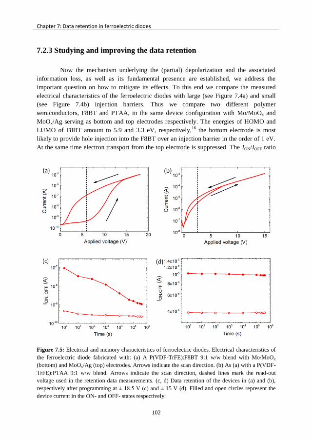
Chapter 7: Data retention in ferroelectric diodes
102
7.2.3 Studying and improving the data retention
Now the mechanism underlying the (partial) depolarization and the associated
information loss, as well as its fundamental presence are established, we address the
important question on how to mitigate its effects. To this end we compare the measured
electrical characteristics of the ferroelectric diodes with large (see Figure 7.4a) and small
(see Figure 7.4b) injection barriers. Thus we compare two different polymer
semiconductors, F8BT and PTAA, in the same device configuration with Mo/MoOx and
MoOx/Ag serving as bottom and top electrodes respectively. The energies of HOMO and
LUMO of F8BT amount to 5.9 and 3.3 eV, respectively,16
the bottom electrode is most
likely to provide hole injection into the F8BT over an injection barrier in the order of 1 eV.
At the same time electron transport from the top electrode is suppressed. The ION/IOFF ratio
Figure 7.5: Electrical and memory characteristics of ferroelectric diodes. Electrical characteristics of
the ferroelectric diode fabricated with: (a) A P(VDF-TrFE):F8BT 9:1 w/w blend with Mo/MoOx
(bottom) and MoOx/Ag (top) electrodes. Arrows indicate the scan direction. (b) As (a) with a P(VDF-
TrFE):PTAA 9:1 w/w blend. Arrows indicate the scan direction, dashed lines mark the read-out
voltage used in the retention data measurements. (c, d) Data retention of the devices in (a) and (b),
respectively after programming at ± 18.5 V (c) and ± 15 V (d). Filled and open circles represent the
device current in the ON- and OFF- states respectively.

Studying and improving the data retention
103
measured at the read-out voltage yields more than two orders of magnitude. It has to be
noted that both ION and IOFF currents in Figure 7.5a are larger compared to the device in
Figure 7.1a. This is most likely related to differences in build-in field due to the different
bottom electrodes and to batch-to-batch variations in the semiconductor.
To record the data in Figure 7.5b the same electrodes as in the case of Figure 7.5a
were used, but F8BT was replaced with PTAA. Since for PTAA the HOMO and LUMO
levels are at 5.25 and 2.3 eV, respectively,22
the bottom electrode now provides hole
injection into the PTAA over a low injection barrier in the order of 0.25 eV. At the same
time electron transport from the top electrode remains suppressed. It is not surprising that
such a small injection barrier leads to a low ION/IOFF ratio, in this case of about 2.5. It has to
be noted that the difference between ION and IOFF currents originates truly from the injection
barrier modulation and not from spurious effects associated e.g. with ionic impurities in the
semiconductor. This we ruled out by measuring (hysteresis free) I-V characteristics for a
bulk PTAA device with the same electrodes and at the same sweep speed (see Figure 7.6).
Figure 7.6: Current vs. voltage (I-V) characteristics of PTAA semiconductor-only diode with
Mo/MoOx (bottom) and MoOx/Ag (top) electrodes. The diode is swept between + 10 and - 10 V.
Arrows indicate the scan direction. Sweep speed is comparable to Figure 7.4b.
Figure 7.5c and Figure 7.5d show the data retention of both types of the devices. It
is clear that the data retention of diode with large injection barrier, based on the F8BT,
shows a similar trend as in Figure 7.1. At the same time the PTAA-based device shows a
significant improvement as the ON-state is hardly affected during the course of the
measurement. Figure 7.7 shows a joint plot of the normalized ION/IOFF ratio obtained from
Figure 7.5c,d. Intuitively this result can be directly linked to the depolarization
phenomenon at the semiconductor/ferroelectric interface as described in Figure 7.3. The
diode with low injection barriers relies to a much lesser degree on the ferroelectric
polarization charges than the one with large injection barriers. At the same time the
absolute ION/IOFF ratio of the F8BT-based device is always greater than the PTAA-based
one.

Chapter 7: Data retention in ferroelectric diodes
104
Figure 7.7: Comparison of the normalized ION/IOFF ratio as measure for the relative data retention of
the ferroelectric diodes in Figure 7.5c,d. Red and blue curves correspond to devices based on the
PTAA (low injection barrier) and F8BT (high injection barrier) semiconductors respectively.
In order to substantiate the interpretation of the measurements presented above a
2D model for the charge transport in the ferroelectric diode was employed.5 The phase
separated morphology is simplified to a 2D structure of alternating ferroelectric and
semiconducting slabs. Motion of electrons and holes and the electrostatic potential are
described by the transport, continuity, and Poisson equations that are numerically solved on
a rectangular grid. The parameters of the blend used in the simulation and the electrical
transport model are explained in detail in the Experimental section and Appendix B
respectively.
Figure 7.8a shows calculated absolute ION and IOFF currents versus the ferroelectric
polarization of the diodes with injection barriers. As expected the ION/IOFF ratio of the diode
is directly correlated with the injection barrier height. The magnitudes of the ON-currents
are in good agreement with the experimentally obtained ones; the OFF-currents are
underestimated due to the absence of leakage in the simulations.5 More importantly, when
the polarization charge density is reduced, corresponding to depolarization in the interfacial
areas in the actual experiment (see Figure 7.3), the ON-current decreases. This increase is
more pronounced and sets in earlier for devices with a high injection barrier, c.f. Figure
7.5c,d. Figure 7.8b shows the corresponding normalized ION/IOFF ratio, its inset shows the
absolute ION/IOFF ratio. Again, reading the polarization charge in the decreasing direction as
a measure of time in the experiment, the similarity to Figure 7.6 is striking. Note in
particular that due to the self-limiting nature of the depolarization process, see the
discussion at Figure 7.3, the polarization charge will not vanish completely for long times.
Hence from the numerical model a finite retention at long times is expected. Like in the
experiment, the ION current of the device with largest injection barrier is most sensitive to
polarization loss but has the largest ION/IOFF ratio. This means that the cost of longer
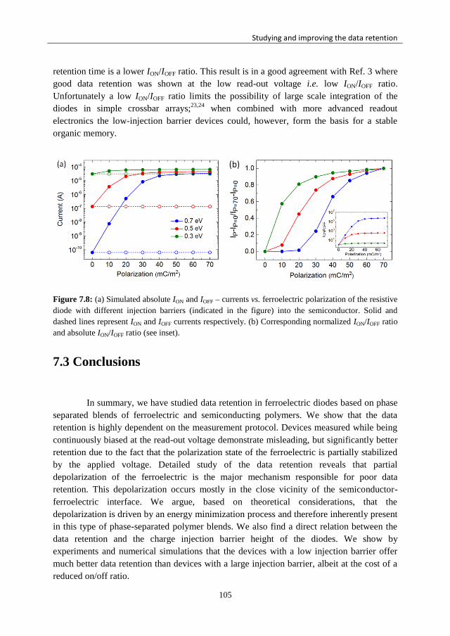
Studying and improving the data retention
105
retention time is a lower ION/IOFF ratio. This result is in a good agreement with Ref. 3 where
good data retention was shown at the low read-out voltage i.e. low ION/IOFF ratio.
Unfortunately a low ION/IOFF ratio limits the possibility of large scale integration of the
diodes in simple crossbar arrays;23,24
when combined with more advanced readout
electronics the low-injection barrier devices could, however, form the basis for a stable
organic memory.
Figure 7.8: (a) Simulated absolute ION and IOFF – currents vs. ferroelectric polarization of the resistive
diode with different injection barriers (indicated in the figure) into the semiconductor. Solid and
dashed lines represent ION and IOFF currents respectively. (b) Corresponding normalized ION/IOFF ratio
and absolute ION/IOFF ratio (see inset).
7.3 Conclusions
In summary, we have studied data retention in ferroelectric diodes based on phase
separated blends of ferroelectric and semiconducting polymers. We show that the data
retention is highly dependent on the measurement protocol. Devices measured while being
continuously biased at the read-out voltage demonstrate misleading, but significantly better
retention due to the fact that the polarization state of the ferroelectric is partially stabilized
by the applied voltage. Detailed study of the data retention reveals that partial
depolarization of the ferroelectric is the major mechanism responsible for poor data
retention. This depolarization occurs mostly in the close vicinity of the semiconductor-
ferroelectric interface. We argue, based on theoretical considerations, that the
depolarization is driven by an energy minimization process and therefore inherently present
in this type of phase-separated polymer blends. We also find a direct relation between the
data retention and the charge injection barrier height of the diodes. We show by
experiments and numerical simulations that the devices with a low injection barrier offer
much better data retention than devices with a large injection barrier, albeit at the cost of a
reduced on/off ratio.

Chapter 7: Data retention in ferroelectric diodes
106
7.4 Experimental
Poly[(9,9-di-n-octylfluorenyl-2,7-diyl) – alt ‒ (benzo[2,1,3]thiadiazol-4,8-diyl)]
F8BT (Mn = 4.9 kDa, D = 1.8) was synthesized according to a modified Suzuki
polymerization.25,26
Poly(bis(4-phenyl)2,3,4-trimethylphenyl)amine PTAA (Mn = 17.5 kDa)
was purchased from Flexink and used as received. The ferroelectric polymer,
poly(vinylidene fluoride-trifluoroethylene) P(VDF-TrFE) (Mn = 220 kDa, 2.3 < D < 2.8
with a 77/23 VDF/TrFe ratio) was supplied by Solvay Specialty Polymers. Blend solution
of P(VDF-TrFE):F8BT was prepared by co-dissolving P(VDF-TrFE) and F8BT (9:1 w/w)
in a mixture of cyclohexanone and tetrahydrofuran 75:25 (v/v) at 50 °C overnight (50
mg/mL). P(VDF-TrFE):PTAA solution was prepared with the same ratio according to the
same recipe with a single solvent cyclohexanone. Cleaned glass substrates with
lithographically patterned Au/MoOx and Mo/MoOx contact electrodes of 0.44 mm2 were
used. Blend films were then spin coated in a nitrogen-filled glove box. The average film
thickness was measured with a DEKTAK profilometer and found to be ≈ 200 ± 10 nm.
Subsequently, the samples were annealed at 135 °C for 1 hour followed by the
deposition of the corresponding Ba/Al or MoOx/Au top electrode. Ferroelectric capacitors
with Au/MoOx and Ba/Al electrodes were made according to the same fabrication recipe
mentioned above using the same solvent mixture as for P(VDF-TrFE):F8BT.
The 2D drift-diffusion model used for simulating the ferroelectric diodes takes into
account the phase separated morphology, which is approximated by alternating slabs of
ferroelectric and semiconductor materials such that both materials are always in contact
with both electrodes (see Figure 1.5c, Chapter 1). Zero mobility is assumed for the
electrically insulating ferroelectric P(VDF-TrFE). In the ferroelectric slab a surface
polarization charge density σp ≈ 70 mC/m2 and a static relative dielectric constant εr = 10
were used. The organic semiconducting slabs were characterized by a typical (constant)
hole mobility, μp = 6.5 × 10⁻¹¹
m2/(V·s), and εr = 3. A field-dependent charge injection into
the semiconductor over a barrier of finite height is implemented by using the
Emtage/O’Dwyer model.27,28
Further details on the model can be found in Ref. 5, 6 and
Appendix B.
7.5 References
[1] J.S. Meena, S.M. Sze, U. Chang, T.-Y. Tseng, Overview of emerging nonvolatile memory
technologies, Nanoscale Res. Lett. 2014, 9, 526.
[2] S.-T. Han, Y. Zhou, V.A.L. Roy¸ Towards the development of flexible non-volatile
memories, Adv. Mater. 2013, 25, 5425.
[3] K. Asadi, D. M. de Leeuw, B. de Boer, P.W.M. Blom, Organic non-volatile memories from
ferroelectric phase-separated blends, Nat. Mater. 2008, 7, 547.
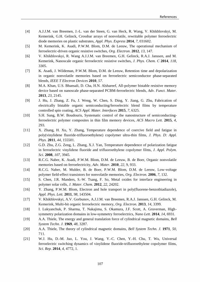
References
107
[4] A.J.J.M. van Breemen, J.-L. van der Steen, G. van Heck, R. Wang, V. Khikhlovskyi, M.
Kemerink, G.H. Gelinck, Crossbar arrays of nonvolatile, rewritable polymer ferroelectric
diode memories on plastic substrates, Appl. Phys. Express 2014, 7, 031602.
[5] M. Kemerink, K. Asadi, P.W.M. Blom, D.M. de Leeuw, The operational mechanism of
ferroelectric-driven organic resistive switches, Org. Electron. 2012, 13, 147.
[6] V. Khikhlovskyi, R. Wang A.J.J.M. van Breemen, G.H. Gelinck, R.A.J. Janssen, and M.
Kemerink, Nanoscale organic ferroelectric resistive switches, J. Phys. Chem. C 2014, 118,
3305.
[7] K. Asadi, J. Wildeman, P.W.M. Blom, D.M. de Leeuw, Retention time and depolarization
in organic nonvolatile memories based on ferroelectric semiconductor phase-separated
blends, IEEE T Electron Devices 2010, 57.
[8] M.A. Khan, U.S. Bhansali, D. Cha, H.N. Alshareef, All-polymer bistable resistive memory
device based on nanoscale phase-separated PCBM-ferroelectric blends, Adv. Funct. Mater.
2013, 23, 2145.
[9] J. Hu, J. Zhang, Z. Fu, J. Weng, W. Chen, S. Ding, Y. Jiang, G. Zhu, Fabrication of
electrically bistable organic semiconducting/ferroelectric blend films by temperature
controlled spin coating, ACS Appl. Mater. Interfaces 2015, 7, 6325.
[10] S.H. Sung, B.W. Boudouris, Systematic control of the nanostructure of semiconducting-
ferroelectric polymer composites in thin film memory devices, ACS Macro Lett. 2015, 4,
293.
[11] X. Zhang, H. Xu, Y. Zhang, Temperature dependence of coercive field and fatigue in
poly(vinylidene fluoride-trifluoroethylene) copolymer ultra-thin films, J. Phys. D: Appl.
Phys. 2011, 44, 155501.
[12] G.D. Zhu, Z.G. Zeng, L. Zhang, X.J. Yan, Temperature dependence of polarization fatigue
in ferroelectric vinylidene fluoride and trifluoroethylene copolymer films, J. Appl. Polym.
Sci. 2008, 107, 3945.
[13] R.C.G. Naber, K. Asadi, P.W.M. Blom, D.M. de Leeuw, B. de Boer, Organic nonvolatile
memories based on ferroelectricity, Adv. Mater. 2010, 22, 9, 933.
[14] R.C.G. Naber, M. Mulder, B. de Boer, P.W.M. Blom, D.M. de Leeuw, Low-voltage
polymer field-effect transistors for nonvolatile memories, Org. Electron. 2006, 7, 132.
[15] S. Chen, J.R. Manders, S.-W. Tsang, F. So, Metal oxides for interface engineering in
polymer solar cells, J. Mater. Chem. 2012, 22, 24202.
[16] Y. Zhang, P.W.M. Blom, Electron and hole transport in poly(fluorene-benzothiadiazole),
Appl. Phys. Lett. 2011, 98, 143504.
[17] V. Khikhlovskyi, A.V. Gorbunov, A.J.J.M. van Breemen, R.A.J. Janssen, G.H. Gelinck, M.
Kemerink, Multi-bit organic ferroelectric memory, Org. Electron. 2013, 14, 3399.
[18] I. Lukyanchuk, P. Sharma, T. Nakajima, S. Okamura, J.F. Scott, A. Gruverman, High-
symmetry polarization domains in low-symmetry ferroelectrics, Nano Lett. 2014, 14, 6931.
[19] A.A. Thiele, The energy and general translation force of cylindrical magnetic domains, Bell
System Techn. J. 1969, 48, 3287.
[20] A.A. Thiele, The theory of cylindrical magnetic domains, Bell System Techn. J. 1971, 50,
711.
[21] W.J. Hu, D.-M. Juo, L. You, J. Wang, Y.-C. Chen, Y.-H. Chu, T. Wu, Universal
ferroelectric switching dynamics of vinylidene fluoride-trifluoroethylene copolymer films,
Sci. Rep. 2014, 4, 4772, 1.

References
108
[22] A. Intaniwet, C.A. Mills, P.J. Sellin, M. Shkunov, J.L. Keddie, Achieving a stable time
response in polymeric radiation sensors under charge injection by X-rays, Appl. Mater.
Inter. 2010, 2, 6, 1692.
[23] N. Pimparkar, Q. Cao, J.A. Rogers, M.A. Alam, Theory and practice of 'striping' for
improved ON/OFF ratio in carbon nanonet thin film transistors, Nano Res. 2009, 2, 167
175.
[24] W.A. Goddard III, D. Brenner, S.E. Lyshevski, G.J. Iafrate, Handbook of nanoscience,
engineering, and technology, Third Edition, 2012, 11-25, CRC Press.
[25] T. van Woudenbergh, J. Wildeman, P.W.M. Blom, J.J.A.M. Bastiaansen, B.M.W.
Langeveld-Voss, Electron-enhanced hole injection in blue polyfluorene-based polymer
light-emitting diodes, Adv. Funct. Mater. 2004, 14, 677.
[26] N. Miyaura, A. Suzuki, Palladium-catalyzed cross-coupling reactions of organoboron
compounds, Chem. Rev. 1995, 96, 2457.
[27] P.R. Emtage, J.J. O’Dwyer, Richardson−Schottky effect in insulators, Phys. Rev. Lett. 1966,
16, 356.
[28] J.J.M. van der Holst, M.A. Uijttewaal, R. Balasubramanian, R. Coehoorn, P.A. Bobbert,
G.A. de Wijs, R.A. de Groot, Modeling and analysis of the three-dimensional current
density in sandwich-type single-carrier devices of disordered organic semiconductors, Phys.
Rev. B 2009, 79, 085203.
109
Appendix A
Confirmation of the working mechanism of the
ferroelectric diode at the local scale
In Chapter 3, the operating mechanism of the ferroelectric diode at the nanometer
scale was studied. A key part of the work relies on the C-AFM experiment where it was
shown that the current injection occurs in the vicinity of the semiconductor/ferroelectric
interface. Its complexity leads to concerns related to the tip resolution and tip-sample
contact radius. In order to confirm the working mechanism of the device at the nanoscale,
Figure A.1: C-AFM‒images (5 × 2 µm2) of a P(VDF-TrFE):F8BT (9:1 w/w) blend on Au. (a)
Topography (total vertical scale ‒ 70 nm). (b) Corresponding current map. (c) Current cross-section
over the conductive domain of diameter 600 nm indicated by the red line in b.
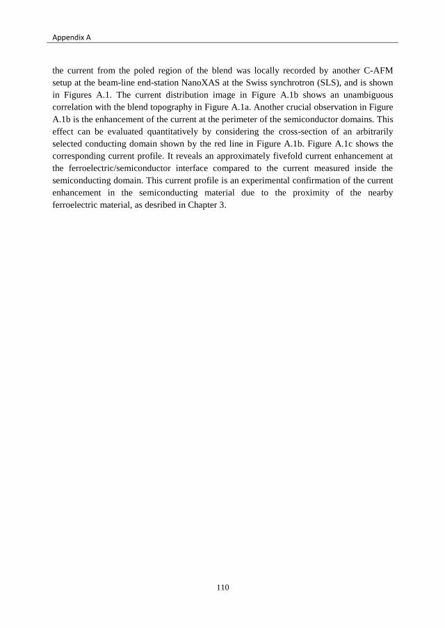
Appendix A
110
the current from the poled region of the blend was locally recorded by another C-AFM
setup at the beam-line end-station NanoXAS at the Swiss synchrotron (SLS), and is shown
in Figures A.1. The current distribution image in Figure A.1b shows an unambiguous
correlation with the blend topography in Figure A.1a. Another crucial observation in Figure
A.1b is the enhancement of the current at the perimeter of the semiconductor domains. This
effect can be evaluated quantitatively by considering the cross-section of an arbitrarily
selected conducting domain shown by the red line in Figure A.1b. Figure A.1c shows the
corresponding current profile. It reveals an approximately fivefold current enhancement at
the ferroelectric/semiconductor interface compared to the current measured inside the
semiconducting domain. This current profile is an experimental confirmation of the current
enhancement in the semiconducting material due to the proximity of the nearby
ferroelectric material, as desribed in Chapter 3.
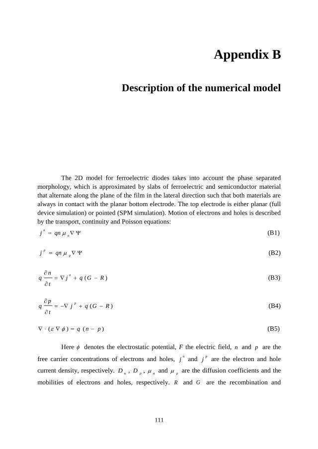
111
Appendix B
Description of the numerical model
The 2D model for ferroelectric diodes takes into account the phase separated
morphology, which is approximated by slabs of ferroelectric and semiconductor material
that alternate along the plane of the film in the lateral direction such that both materials are
always in contact with the planar bottom electrode. The top electrode is either planar (full
device simulation) or pointed (SPM simulation). Motion of electrons and holes is described
by the transport, continuity and Poisson equations:
n
nqnj (B1)
p
pqnj (B2)
)( RGqjt
nq
n
(B3)
)( RGqjt
pq
p
(B4)
)()( pnq (B5)
Here denotes the electrostatic potential, F the electric field, n and p are the
free carrier concentrations of electrons and holes, n
j and p
j are the electron and hole
current density, respectively. n
D , p
D , n
and p
are the diffusion coefficients and the
mobilities of electrons and holes, respectively. R and G are the recombination and

Appendix B
112
(photo) generation rate, respectively. The generation rate is set to zero. 0
r
with 0
the permittivity of vacuum and r
the relative permittivity.
The recombination rate is given by the Langevin expression:
npR (B6)
with
np
(B7)
Note that the use of the transport equation implies the validity of the Einstein
relation:
pn
B
pn
q
TkD (B8)
Here, B
k is the Boltzmann constant, T the temperature, and q the elementary
charge.
Eqs. B1‒B5 are solved on a rectangular 2D grid. Periodic boundary conditions on
the left and right hand sides are used, effectively making the simulated device an infinite
repetition of alternating slabs of ferroelectric and semiconductor material.
A Boltzmann factor for the hole and electron densities p0, n0 at the bottom contact
is used as boundary condition for the density in the semiconductor:
Tk
qNp
B
p
exp00
(B9)
Tk
qNn
B
n
exp00
(B10)
Appendix B: Description of the numerical model
113
The np .
are the effective hole and injection barriers that must add up to the
HOMO-LUMO gap, viz. gnp
E . The boundary condition at the top contact is a
similar Boltzmann factor. The injection barriers np /
may be reduced to an effective
injection barrier pn /
by the image potential, in which case:
r
pnpn
Fq
0
//
4 (B11)
The square root term in Eq. B11 only applies when the electric field F is directed
to (away from) the contact so electron (hole) injection is facilitated. This model is referred
to as the Emtage O'Dwyer model and gives rise to a field dependent charge injection.
In the ferroelectric slab a surface polarization charge density ±σp can be fixed on
the second and the next to the last grid points, i.e. above the bottom electrode and below the
top electrode. The first and the last grid points are filled with the spacer material and
screening charges respectively. The sign depends on the polarization direction.
A bias V may be applied between the contacts by setting the electrostatic potential
at the top contact at –qV while keeping the potential of the bottom contact at zero.
Solutions to Eqs. B1‒B5 are obtained by setting the appropriate boundary
conditions for n, p and at the start of the simulation at t = 0. For the rest, the device is
taken to be depleted of mobile charges at t = 0. In subsequent small time steps, currents are
calculated from Eqs. B1‒B2, which, for each time step, give rise to a change in the carrier
density according to Eqs. B3‒B4 and to a new electrostatic potential according to Eq. B5.
The changed field at the contacts translates into a change in the boundary conditions Eqs.
B9,10 via Eq. B11. Steady state is reached when currents and carrier densities no longer
change.

Appendix B
114

115
Summary
Organic Ferroelectric Diodes
Today’s world demands a special type of electronics. Those new devices will look
nothing like rigid metal and plastic boxes. Instead, they will be extremely light, soft,
flexible, transparent, cheap or a combination thereof, and can be integrated into everyday
objects like paper, clothes and packaging material. The ferroelectric diode could be a very
attractive information storage element in this type of electronics because it can be processed
from solution on rigid and flexible plastic substrates at low temperatures. Other important
features of this device are architectural simplicity and the possibility of non-destructive
read out, making it an extremely promising candidate for large-area, low-cost, non-volatile
reprogrammable memory applications in general.
The aim of the research described in this thesis is the understanding-based
development, characterization and optimization of ferroelectric memory devices, i.e.
capacitors and diodes.
In Chapter 2, a multi-bit organic ferroelectric-based non-volatile memory with
binary readout from a simple capacitor structure is introduced. The functioning of the
multi-bit concept is quite generally applicable and depends on the following properties for
the data storage medium: (a) The data storage medium effectively consists of microscopic
switching elements ('hysterons'). (b) The positive and negative coercive fields of each
hysteron are equal in magnitude. (c) The distribution of hysteron coercive fields has
substantial width. It is shown that the organic ferroelectric copolymer P(VDF-TrFE) meets
these requirements. All basic properties of our device are measured and modeled in the
framework of the dipole switching theory. As a first example the possibility to
independently program and subsequently read out the lower, middle and upper parts of the
hysteron distribution function, yielding a 3-bit memory in a single capacitor structure, is
shown. All measured devices show good state reproducibility, high endurance and
potentially great scalability.
In Chapter 3, various scanning probe techniques are combined with numerical
modeling to unravel the operational mechanism of ferroelectric diodes. It is shown that the
resistive switching results from modulation of the charge injection barrier at the
semiconductor-electrode interfaces. The modulation is driven by the stray field of the
Summary
116
polarization charges in the ferroelectric phase, and consequently is restricted to regions
where semiconductor and ferroelectric phases exist in close vicinity. Since each
semiconductor domain can individually be switched and read out, a novel, nanoscale
memory element is demonstrated. An ultimate information density of ≈ 30 Mb/cm2 is
estimated for this bottom-up defined memory device.
In Chapter 4, a simple approach to study the full 3D morphology of phase-
separated blends, taking advantage of the possibility to selectively dissolve the different
components is introduced. This method is applied in combination with AFM to investigate
a blend of a semiconducting and ferroelectric polymer that is typically used as active layer
in ferroelectric diodes. It is found that the blend consists of a ferroelectric matrix with three
types of embedded semiconductor domains and a thin wetting layer at the bottom electrode.
Statistical analysis of the obtained images excludes the presence of a fourth type of
domains. Criteria for the applicability of the presented technique are discussed as well.
In Chapter 5, the possibility to direct the semiconducting domains of a phase-
separating mixture of P(VDF-TrFE) and F8BT in a thin film into a highly ordered 2D
lattice by means of surface directed phase separation is demonstrated. Numerical simulation
of the surface-controlled de-mixing process provides insight in the ability of the substrate
pattern to direct the phase separation, and hence the regularity of the domain pattern in the
final dry blend layer. By optimizing the ratio of the blend components, the number of
electrically active semiconductor domains is maximized. Pattern replication on a cm-scale
was achieved, and improved functional device performance is demonstrated in the form of
a tenfold increase of the ON-current and a sixfold increase in current modulation. This
approach therefore provides a simple and scalable means to higher density integration, the
ultimate target being a single semiconducting domain per memory cell.
In Chapter 6, the device structure and its impact on the device performance are
studied by advanced scanning probe techniques. It is found that a thin wetting layer
drastically influences the device performance by hindering the ferroelectric polarization in
one of the bias directions. An optimal and simple fabrication recipe to avoid the formation
of this wetting layer is found. The new fabrication provides an improved blend structure
that offers better device performance.
In Chapter 7, the data retention of the devices is characterized, understood and
controlled. First, it is shown that the measurement protocol can strongly affect the 'apparent'
retention time and a suitable protocol is identified. Second, it is shown by experimental and
theoretical methods that partial depolarization of the ferroelectric is the major mechanism
responsible for imperfect data retention. This depolarization occurs in close vicinity to the
semiconductor-ferroelectric interface, is driven by energy minimization and is inherently
present in this type of phase-separated polymer blends. Third, a direct relation between data
retention and the charge injection barrier height of the diode is demonstrated
experimentally and numerically. Tuning the injection barrier height allows to improve
retention by many orders of magnitude in time, albeit at the cost of a reduced
Summary
117
on/off ratio.
To summarize, this thesis describes the local working mechanism, structure and
data retention of ferroelectric memory diodes based on phase separated blends of
ferroelectric and semiconductor polymers. The operational mechanism of the device is
studied at the device level and at the nanoscale by various scanning probe techniques,
leading to a fully quantitative device model. In addition a simple approach to study the full
3D morphology of the blend, taking advantage of the possibility to selectively dissolve the
different components, is introduced. In combination with the developed methods to control
the phase separated morphology, this allows to improve the device performance in a
rational manner. The most important result obtained in this work is that the data retention is
intimately linked to the morphology of the phase-separated polymer blend and is due to
polarization loss in a narrow region around the semiconducting domains. Mitigation of this
fundamental problem is possible by tuning the injection barrier height of the device, albeit
at the cost of a reduced on/off ratio. An alternative strategy could be to use a semiconductor
with a high dielectric constant, which reduces the driving force for depolarization. This
might improve the data retention of the devices since it should slow down the
depolarization process in the ferroelectric matrix.

Summary
118

119
Samenvatting
De wereld van vandaag vraagt om een special type elektronica. Deze nieuwe
elektronica zal niet bestaan uit hard metaal en plastic behuizingen. Integendeel, het zal
extreem licht, zacht, flexibel, transparant, goedkoop of een combinatie van dit alles zijn en
zal geïntegreerd kunnen worden in dingen als papier, kleding en verpakkingsmateriaal. De
ferroelektrische diode zou een zeer aantrekkelijke informatieopslagelement kunnen zijn in
dit type elektronica, omdat het vanuit oplossing geproduceerd kan worden op zowel stugge
als flexibele substraten bij lage temperatuur. Andere belangrijke kenmerken van deze
component zijn de eenvoudige architectuur en de mogelijkheid om niet-destructief uit te
lezen. Dit maakt het een zeer beloftevolle kandidaat voor groot-oppervlakte, goedkope,
herprogrammeerbaar permanent geheugentoepassing en in het algemeen.
Het doel van het onderzoek zoals beschreven in dit proefschrift is de op begrip
gebaseerde ontwikkeling, karakterisatie en optimalisatie van ferroelektrisch geheugen,
zoals condensatoren en diodes.
In Hoofdstuk 2, wordt een multibit organisch permanent geheugen geïntroduceerd
gebaseerd op ferroelektriciteit met een binaire uitleesmogelijkheid via een simpele
condensatorstructuur. Het functioneren van dit multibitconcept is vrij algemeen toepasbaar
en hangt af van de volgende eigenschappen van het opslagmedium: (a) Het opslagmedium
bestaat effectief uit microscopische schakelaarelementen ('hysteronen'). (b) De positieve en
negatieve coërcieve velden van elk hysteron zijn gelijk in grootte. (c) De verdeling van
coërcieve velden van de hysteronen heeft een behoorlijke breedte. Er wordt aangetoond dat
het organische ferroelektrische copolymeer P(VDF-TrFE) voldoet aan deze voorwaarden.
Alle basiseigenschappen van onze component zijn gemeten en gemodelleerd binnen het
raamwerk van de dipoolschakeltheorie. Als een eerste voorbeeld, wordt de mogelijkheid
om het lage, midden en hoge gedeelte van de hysteronverdelingsfunctie onafhankelijk te
programmeren en daaropvolgend uit te lezen getoond, wat een 3-bits geheugen in een
enkele condensatorstructuur oplevert. Alle gemeten componenten laten een goede
reproduceerbaarheid van de toestand, een hoog uithoudingsvermogen en een potentieel
grote schaalbaarheid zien.
Samenvatting
120
In Hoofdstuk 3, worden verschillende scanning probe technieken gecombineerd
met numeriek modelleren om het operationele mechanisme van organische ferroelektrische
weerstandsschakelaars te ontrafelen. Er wordt getoond dat het weerstandsschakelen het
resultaat is van het moduleren van de ladingsinjectiebarrière aan de halfgeleider-
elektrodegrensvlakken. De modulatie wordt gedreven door de strooivelden van de
polarisatielading in de ferroelektrische fase, en beperkt zich dus tot de regio’s waar de
halfgeleider en ferroelektrische fasen naast elkaar bestaan. Aangezien elk
halfgeleiderdomein individueel geschakeld en uitgelezen kan worden, is dit een
demonstratie van een nieuw geheugenelement op de nanoschaal. Er wordt een ultieme
informatiedichtheid van ≈ 30 Mb/cm2 geschat voor deze bottom-up gedefinieerde
geheugencomponent.
In Hoofdstuk 4, wordt een eenvoudige aanpak geïntroduceerd om de volledige 3D
morfologie van de fasegescheiden mengsels te bestuderen, gebruik makend van de
mogelijkheid om selectief de verschillende componenten op te lossen. Deze methode wordt
toegepast in combinatie met AFM om een mengsel van een halfgeleidend en ferroelektrisch
polymeer te onderzoeken dat typisch gebruikt wordt als actieve laag in ferroelektrische
diodes. Het blijkt dat het mengsel bestaat uit een ferroelektrische matrix met drie types van
ingesloten halfgeleidende domeinen en een dunne bevochtigende laag op de
bodemelektrode. Statistische analyse van de verkregen beelden sluit de aanwezigheid van
een vierde type domein uit. Ook worden criteria voor de toepasbaarheid van de
gepresenteerde techniek besproken.
In Hoofdstuk 5, wordt de mogelijkheid om de halfgeleidende domeinen van een
fasescheidende mix van P(VDF-TrFE) en F8BT in een dunne film te sturen naar een sterk
geordend 2D rooster door middel van oppervlakgerichte fasescheiding gedemonstreerd.
Numerieke simulaties van het door het oppervlak gecontroleerde ontmengingsproces geven
inzicht in hoeverre het substraatpatroon de fasescheiding en daarmee de regulariteit van het
domeinpatroon in uiteindelijke droge laag kan sturen. Door de ratio van de componenten
van het mengsel te optimaliseren kan het aantal elektrisch actieve halfgeleiderdomeinen
worden gemaximaliseerd. Patroonreplicatie op een centimeterschaal is bereikt, alsmede een
verbeterde prestatie van de functionele component in de vorm van een tienvoudige toename
van de aan-stroom en een zesvoudige toename in de stroommodulatie. Deze aanpak biedt
derhalve een simpele en schaalbare methode om hogere integratiedichtheden te realiseren,
met als uiteindelijk doel een enkel halfgeleiderdomein per geheugencel.
In Hoofdstuk 6, wordt de componentstructuur en de invloeden op de prestaties
daarvan bestudeerd met geavanceerde scanning probe technieken. Het blijkt dat de
bevochtigingslaag de prestaties drastisch beïnvloed door het hinderen van de
ferroelektrische polarisatie in een van de spanningsrichtingen. Er is een optimaal en
eenvoudig fabricagerecept gevonden om de formatie van deze bevochtigingslaag te
voorkomen. De nieuwe fabricage biedt een verbeterde structuur van het mengsel wat een
betere prestatie oplevert.

Samenvatting
121
In Hoofdstuk 7, wordt de dataretentie van de componenten gekarakteriseerd,
verklaard en beheerst. Eerst wordt er getoond dat het meetprotocol een sterk effect kan
hebben op de 'schijnbare' retentietijd en wordt er een passend protocol geïdentificeerd. Ten
tweede wordt er door middel van experimentele en theoretische methoden aangetoond dat
gedeeltelijke depolarisatie van het ferroelektricum het hoofdmechanisme is dat
verantwoordelijk is voor de imperfecte dataretentie. Deze depolarisatie treedt op in de buurt
van het halfgeleider-ferroelektricum interface, wordt gedreven door minimalisatie van de
energie en is intrinsiek aanwezig in dit soort fasegescheiden polymere mengsels. Ten derde
wordt een direct verband tussen de dataretentie en de hoogte van de ladingsinjectiebarrière
van de diode experimenteel en numeriek aangetoond. Het afstemmen van de
injectiebarrièrehoogte kan de retentietijd met ordes van grootte verbeteren, al zij het tegen
de prijs van een verminderde aan/uitratio.
Samenvattend, dit proefschrift beschrijft de lokale werking, structuur en
dataretentie van ferroelektrische geheugendiodes gebaseerd op fasegescheiden mengsels
van ferroelektrische en halfgeleidende polymeren. De werking van de component is
bestudeerd op componentniveau en op de nanoschaal door middel van verschillende
scanning probe technieken, leidend tot een volledig kwantitatief componentmodel.
Daarbovenop is er een eenvoudige aanpak om de volledige 3D morfologie van het mengsel
te bestuderen geïntroduceerd. In combinatie met de ontwikkelde methodes om de
fasegescheiden morfologie te sturen, biedt dit de mogelijkheid om de prestaties op een
rationele manier te verbeteren. Het belangrijkste resultaat verkregen uit dit werk is dat de
dataretentie sterk verbonden is met de morfologie van het fasegescheiden polymeermengsel
omdat polarisatieverlies optreedt in een smalle regio rondom het halfgeleidende domein.
Dit fundamentele probleem is te vermijden door de hoogte van de injectiebarrière af te
stemmen, zij het tegen de prijs van een verminderde aan/uitratio. Een alternatieve strategie
zou het gebruik van een halfgeleider met een hoge diëlektrische constante zijn, hetgeen de
drijvende kracht voor depolarisatie vermindert. Dit zou de dataretentie van de componenten
kunnen verbeteren, aangezien dit het depolarisatieproces in de ferroelektrische matrix zou
moeten vertragen.

Samenvatting
122

123
Curriculum Vitae
Vsevolod Khikhlovskyi was born on the 1st of December 1985 in Zhovti Vody,
Ukraine. After finishing high school in 2003 at the Lyceum in Zhovty Vody, he studied
Applied Physics and Electronics at Kyiv National Taras Shevchenko University in Kyiv,
Ukraine. In 2009 he was awarded a scholarship for the Top Master Program in Nanoscience
at the University of Groningen, The Netherlands. His master graduation project was
focused on the nanoscale electronic transport in metal and oxide based devices. After his
graduation in 2011 he continued as a PhD student in the group Molecular Materials and
Nanosystems at the Eindhoven University of Technology and in the group Organic and
Oxide Transistor/Flexible OLED Displays at the Open Innovation Research and
Development Center Holst Center. His research was done in the field of ferroelectric
diodes. The main results of his PhD research are described in this thesis.

124

125
List of publications
1. V. Khikhlovskyi, A.V. Gorbunov, A.J.J.M. van Breemen, R.A.J. Janssen, G.H. Gelinck,
and M. Kemerink, Multi-bit organic ferroelectric memory, Org. Electron. 2013, 14(12),
3399-3405.
2. V. Khikhlovskyi, R. Wang A.J.J.M. van Breemen, G.H. Gelinck, R.A.J. Janssen, and M.
Kemerink, Nanoscale Organic Ferroelectric Resistive Switches, J. Phys. Chem. C 2014,
118, 3305-3312.
3. A. van Breemen, T. Zaba, V. Khikhlovskyi, J. Michels, R.A.J. Janssen, M. Kemerink,
and G.H. Gelinck, Surface Directed Phase Separation of Semiconductor Ferroelectric
Polymer Blends and their Use in Non-Volatile Memories, Adv. Funct. Mater. 2015, 25,
278-286.
4. V. Khikhlovskyi, A.J.J.M. van Breemen, J.J. Michels, R.A.J. Janssen, G.H. Gelinck and
M. Kemerink, 3D-morphology reconstruction of nanoscale phase-separation in polymer
memory blends, accepted to J. Polym. Sci. Pol. Phys.
5. V. Khikhlovskyi, A.J.J.M. van Breemen, R.A.J. Janssen, G.H. Gelinck and M.
Kemerink, Data retention in organic ferroelectric resistive switches, in preparation.
6. X. Li, A.J.J.M. van Breemen, V. Khikhlovskyi, E.C.P. Smits, M. Kemerink, D.J. Broer,
G.H. Gelinck, Programmable polymer light emitting transistors with ferroelectric
polarization-enhanced channel current and light emission, Org. Electron. 2012, 13, 9, 1742-
1749.
7. A.J.J.M. van Breemen, J.-L. van der Steen, G. van Heck, R. Wang, V. Khikhlovskyi, M.
Kemerink, and G.H. Gelinck, Crossbar arrays of nonvolatile, rewritable polymer
ferroelectric diode memories on plastic substrates. Appl. Phys. Express 2014, 7, 031602.
8. J. Lee, A.J.J.M. van Breemen, V. Khikhlovskyi, M. Kemerink, R.A.J. Janssen, G.H.
Gelinck, Pulse-modulated multilevel data storage in an organic ferroelectric resistive
memory diode, submitted to Adv. Electron. Mater.

126
127
Acknowledgements
This thesis would not have been possible without the help and support of many
people.
First of all, I would like to express my deepest gratitude to my supervisors at the
Eindhoven University of Technology and the Holst Centre Prof. Dr. Martijn Kemerink,
Prof. Dr. Gerwin Gelinck and Prof. Dr. René Janssen.
Martijn, you have been my supervisor at the TU/e for four years. I would like to
thank you for giving me the opportunity to work on this challenging, but very interesting
project. Your style of supervision was a key part of my project. I had freedom to do science
and at the same time I was gently guided by you to the right direction! You have built a
significant part of my personality. Your love and fantastic dedication to science combined
with a positive attitude towards life energize people around you. I am thankful for all the
conferences, workshops, scientific discussions and other activities I was involved in during
my project. What I would like to mention is that you have been supervising me remotely for
about one and half years. It worked out pretty well ‒ you were always there to help me
whenever needed! And of course my congratulations on your promotion to a full professor
position at Linköping University! I wish you good luck in your scientific career and many
exciting publications from your growing group!
Gerwin, you have been supervising me at Holst Centre for four years. I would like
to thank you for allowing me to work on my PhD project at Holst Centre. I enjoyed my
time at Holst Centre ‒ a place where academia and industry meet each other. I learned a lot
from you in terms of science, writing manuscripts, presenting results and time/project
management. You always brought new ideas and excellent suggestions. You are a very
productive and active person; you manage to be everywhere – in science, R&D and
industry. My congratulations on your promotion to a professor position at Eindhoven
University of Technology! I wish you all the best in your future career!
René, my first impression of you and the M2N group was formed when I received
your kind reply on my PhD application ‒ “Dear Seva, Thank you for your e-mail and
application for a PhD position. In our group we have vacancies for PhD students on topics
Acknowledgements
128
related to organic ferroelectrics… Best regards, René Janssen”. My four-year PhD journey
started from that email. The support (in all aspects) and openness from you, René, was
crucial for my PhD project. Your scientific input, especially at the very last stage, was
extremely important for completion of my dissertation. You bring up a relaxing, positive
and at the same time very productive atmosphere to the M2N group. My congratulations on
your SPINOZA Award! “The Award is the ultimate recognition of the great science and
technology of all (former) members of René Janssen’s Group”.
I sincerely acknowledge Dr. Albert van Breemen ‒ my daily supervisor at Holst
Centre. Albert, I learned a lot from you. I was always fascinated with your enthusiasm,
patience, energy and kindness. I am very thankful for your help with my experiments,
manuscripts and for all fruitful discussions we had. Because I called you so many times, I
still remember your phone number by heart . Your contribution was absolutely essential
for the completion of this dissertation.
I am grateful to Dr. Jasper Michels for modeling phase separation in polymer
blends that contributed to the work described in thesis.
I would like to thank Nicolas Pilet, Laetitia Bernard and Peter Warnincke for
organizing research activities in Switzerland. I stayed there for a few days however we
managed to produce data which was important in confirming and strengthening hypothesis.
I would like to thank all the members of my PhD committee: Prof. Dr. Beatriz
Noheda, Prof. Dr. Paul Koenraad, Prof. Dr. Dago de Leeuw, Dr. Stefan Meskers for their
time and efforts that make my defense possible.
I also appreciate Dr. Kees Flipse, Dr. Peter Bobbert and Prof. Dr. Reinder
Coehoorn for their constructive questions and remarks during our weekly group meetings.
I would like to acknowledge Jolanda Kooijmans and Martina Jiricka for their
administrative support during my four years of stay at the TU/e.
Next, I would like to thank our technicians Wijnand Dijkstra and Marco van der
Sluis for their continuous technical support and help. Wijnand, your assistance in the SPM-
related measurements was crucial for my PhD project. Marco, you were always around to
fix/improve our setups. I really appreciate Ton van den Biggelaar, engineer from Philips,
for his eager help with the fabrication whenever required.
I would like to thank several master students at the TU/e and Holst Centre: Rui,
Mina, Tomasz and Jun. All of you helped me a lot during my PhD project and lots of your
results ended up in this thesis.
I would like to acknowledge people from the M2N group at the TU/e: Dr. Martijn
Wienk, Dr. Stefan Meskers, Stephan, Cristian, Kevin, Mohamed, Wijnand, Igor, Ameneh,
Robin, Mike, Andrey, Alice, Hans, Serkan, Harm (thanks for helping me with my
Samenvatting ), Koen, Le, Vikas and Andrea.
Finally, I would like to thank members of the TP5 group and other people from
Holst Centre: Abhishek, Brian, Jan-Laurens, Joris, Karin, Charlotte, Francisco, Juliane,
Santhosh, Ashutosh, Hangxing, Aashini, Madelon and Bas.