optimized phase-shifting masks for high- resolution … baik, hoya corp. usa peter d. buck, mentor...
TRANSCRIPT

PhotomaskPhotomaskBACUS—The international technical group of SPIE dedicated to the advancement of photomask technology.
1045
0-81
N • E • W • S
May 2018 Volume 34, Issue 5
Industry BrIefs—see page 11
CalendarFor a list of meetings —see page 12
Take A Look Inside:
EUVL17 Poster
Optimized phase-shifting masks for high-resolution resist patterning by interference lithographySascha Brose, Serhiy Danylyuk, and Lukas Bahrenberg, Chair for Technology of Optical Systems, RWTH Aachen University, Steinbachstr. 15, 52074 Aachen, Germany; JARA - Fundamentals of Future Information Technology, Julich, Germany
Rainer Lebert, RI Research Instruments GmbH, Friedrich-Ebert-Strabe 1, 51429 Bergisch Gladbach, Germany
Peter Loosen, Chair for Technology of Optical Systems, RWTH Aachen University, Steinbachstr. 15, 52074 Aachen, Germany; JARA - Fundamentals of Future Information Technology, Julich, Germany; Fraunhofer Institute for Laser Technology, Steinbachstr. 15, 52074 Aachen, Germany
Larissa Juschkin, JARA - Fundamentals of Future Information Technology, Julich, Germany; Chair for the Experimental Physics of the EUV, RWTH Aachen University, Steinbachstr. 15, 52074 Aachen, Germany; Research Center Julich, Peter Grunberg Institute 9, JARA-FIT, Wilhelm-Johnen-Strabe, 52428 Julich
ABSTRACTThe EUV laboratory exposure tool (EUV-LET) is a versatile stand-alone resist patterning tool. Main applications are resist characterization for industrial lithography as well as the patterning of high-resolution arrays over large areas as required in research and small-volume production. High-resolution patterns are achieved by interference lithography based on the achromatic Talbot effect. The theoretical resolution limit for achromatic Talbot lithography (ATL) of 10 nm half-pitch (HP) is mainly resist-limited, as long as necessary high-resolution transmission masks can be fabricated. In this paper we focus on the transmission mask fabrication technology with a low number of process steps that allows to maximize yield and offers high flexibility. Diffraction order efficiencies (DOEs) of the masks are optimized to achieve maximal aerial image contrast (MTF) in the achro-
Figure 1. Calculated DOEs of individual DOs (intensities of ±1st DOs summed up) as a function of the polymer thickness at constant fill factor (a) and as a function of the fill factor at constant polymer thickness (b). The blue dashed vertical lines indicate the optimal parameters when masks are used for ATL.

EditorialN • E • W • S
BACUS News is published monthly by SPIE for BACUS, the international technical group of SPIE dedicated to the advancement of photomask technology.
Managing Editor/Graphics Linda DeLano
Advertising Melissa Farlow
BACUS Technical Group Manager Marilyn Gorsuch
■ 2018 BACUS Steering Committee ■
PresidentJim N. Wiley, ASML US, Inc.
Vice-PresidentFrank E. Abboud, Intel Corp.
SecretaryLarry S. Zurbrick, Keysight Technologies, Inc.
Newsletter EditorArtur Balasinski, Cypress Semiconductor Corp.
2018 Annual Photomask Conference ChairsEmily Gallagher, IMEC
Jed Rankin, GLOBALGOUNDRIES Inc.
International ChairUwe F. W. Behringer, UBC Microelectronics
Education ChairFrank E. Abboud, Intel Corp.
Members at LargeMichael D. Archuletta, RAVE LLC
Ki-ho Baik, HOYA Corp. USA Peter D. Buck, Mentor Graphics Corp.
Brian Cha, Samsung Electronics Co., Ltd.Derren Dunn, IBM Corp.
Thomas B. Faure, GLOBALFOUNDRIES Inc.Aki Fujimura, DS2, Inc.
Brian J. Grenon, Grenon ConsultingJon Haines, Micron Technology Inc.
Naoya Hayashi, Dai Nippon Printing Co., Ltd. Bryan S. Kasprowicz, Photronics, Inc.
Patrick M. Martin, Applied Materials, Inc. Kent Nakagawa, Toppan Photomasks, Inc.
Jan Hendrik Peters, bmbg consultMoshe Preil, KLA-Tencor Corp.
Stephen P. Renwick, Nikon Research Corp. of AmericaDouglas J. Resnick, Canon Nanotechnologies, Inc.
Thomas Scheruebl, Carl Zeiss SMT GmbHThomas Struck, Infineon Technologies AG
Bala Thumma, Synopsys, Inc.Anthony Vacca, Automated Visual Inspection
Michael Watt, Shin-Etsu MicroSi Inc.
P.O. Box 10, Bellingham, WA 98227-0010 USATel: +1 360 676 3290Fax: +1 360 647 1445
©2018
All rights reserved.
Challenges of Modern Chip Design - Software PerspectiveEditorial by Bala Thumma, Synopsys
Everyone in the field of chip design and photolithography is familiar with ever increasing complexities in the design and manufacturing process. As feature sizes shrink to the single digit nanometer realm, design complexity and physical effects exceed what probably most people can consider when developing a chip. This is where CAD software comes into play to ensure all boundary conditions, like timing, parasitic effects, cross-talk, quantum effects, power, heat, etc. are taken into account. Use of standard cells, automatic place and route, optical effects correction, atomic level transistor simulation, etc. allow achieving unprecedented time to market for the most advanced IC products.
Data volumes are ever increasing, reaching multiple terabytes of pattern data for single EUV layers at 7nm. Design and manufacturing software responds by becoming ever more scalable, deploying divide and conquer strategies that allow thousands of distributed workers to process data on high performance server farms. While challenging, the positive feedback loop of better compute-hardware enables the processing of these designs. This trend will likely continue until no more shrinking would be possible. At 0.1 nm, we will be dealing with the dimensions of an atom and that would be the end of it.
However, there is a new set of problems arising from the advent of meta materials, optical and mechanical Microsystems (OMEMS) and the inevitable integration of such systems on a chip. Such designs have less automation available during the design process. CAD tools cannot (currently) discern the designer’s intent when drawing curvilinear shapes that make up a lot of such layouts. For example, if two curves touch each other in one point, or if there is a one-address unit gap between two curves, it is not clear if the curves should touch, or stay disconnected. Software can create, or remove, such gaps, or connections, but which is the correct thing to do? Until machine learning matures to the point where it can make educated guesses, it will be up to the designer to ensure they create clean, unambiguous patterns. This becomes so important because all layouts are done on some grid, e.g. 1, 5, 10nm. However, during processing, vertices need to get rounded to a coarser grid to facilitate mask making on e.g. e-beam tools that only support only certain resolution or edge angles. Since neither the MDP software, nor the mask manufacturer, usually know the design intent, unclean layouts might make it all the way to wafer production and then fail at the final step of functional testing. This is obviously a very costly situation to be avoided. So, here is the call to designers. Make sure your output is clean. The age-old rule of engineering applies: garbage in, garbage out.

mask-based interference approaches is defined only by the trans-mission mask and the source emission properties since there are no additional optical elements in the beam path. Moreover, the local mask uniformity requirements are relaxed, since local mask defects can be smoothed out by interference effects10,11. The manufacturing of the masks is also easier than for 1:1 approaches, such as nanoimprint, since the structure sizes on the wafer are typically smaller than on masks12.
The realized EUV laboratory exposure tool (EUV-LET) is based on the achromatic Talbot effect, which is an effective method for sources with broadband emission. The main components of the EUV-LET are the discharge produced plasma (DPP) EUV source13,14, the transmission masks and the high-precision mask and wafer positioning system. Exposures need to be performed within the distance window where a stationary achromatic intensity modula-tion is formed by the source emission and the transmission mask15. For the use of broadband EUV emission the distance window is situated in a sub-150 μm mask-wafer distance and its width is limited by the spatial coherence that can be achieved in the mask plane. The depth-of-field (DOF) of the intensity modulation is 10 to 20 μm which allows for reliable patterning if the mask-wafer distance can be controlled precisely. Within the distance window many DOs are overlapping and contribute to the intensity modula-
matic Talbot distance. The developed four-step mask fabrication process of contact-hole masks with HPs of 50 nm, 40 nm and 30 nm over areas of 1 x 1 mm2 is presented. The transmission masks are characterized within the EUV-LET to determine the achievable MTF that can be used for resist patterning and characterization. Based on the carried out in-tool measurements the achievable MTF is 63.7 % and the total diffraction efficiency into the 1st diffraction orders (DOs) is 41.7 % (both for 50-nm-HP masks) which makes the masks perfectly suited for the achromatic Talbot approach. Furthermore, we demonstrate high-resolution patterning down to 28 nm HP describing an effective in-lab tool that can be used at facilities for the characterization of photoresists for the upcoming lithography generations.
1. IntroductionHigh-resolution nanopatterning techniques are required not only in science and research1-3 but also in the lithographic industry for resist characterization4,5. The quality of the resist pattern in terms of critical dimension uniformity or line edge roughness is directly linked to the quality of the aerial image that is utilized for the exposure of the photoresist6-8. Approaches that are based on interference effects can provide very homogeneous intensity modulations over large areas9. The intensity modulation in the
Figure 4. a) Top-down overview SEM image of 30-nm-HP mask structures (scale bar = 200 nm). Right side: Cross-sectional SEM images of the fabricated mask structures with HPs of 30 nm (b), 40 nm (c) and 50 nm (d) (scale bar = 100 nm). The Pt-layer is deposited only for sample preparation and penetrates into the polymer openings.
Figure 2. Schematic cross-sectional view of the four main process steps in the mask fabrication. The different layer materials are indicated by different colors.
Figure 3. Monte Carlo simulation on the electron trajectories for the different layer systems. Comparison of the influence of the substrate and the acceleration voltage on the deposited energy density per injected electron in distance to the electron injection point.
Volume 34, Issue 5 Page 3
N • E • W • S
tion leading to a high throughput with typical exposure times of several seconds for EUV-resists. Size-scalable single exposure fields of several square millimeters can be achieved and repeated to cover even larger areas since no unused DOs surround the pat-terned field at this short exposure distance11.
The transmission masks are the key elements of this approach and need to be fabricated for each target HP size. Efficient fabri-cation of the masks has been achieved by minimizing the number of required process steps. Optimized parameters for the electron beam lithography of a spin-on polymer on an ultrathin membrane lead to high-aspect ratio mask structures. The developed mask fabrication process and the realized mask structures are presented in the first section. The polymer thickness of the transmission masks is optimized to achieve maximum 1st DOE and low inten-sity into the 0th DO which will result in high aerial image contrast (described as the modulation transfer function, MTF) at the ex-posure distances for ATL. For the pre-exposure characterization, the fabricated transmission masks are mounted onto a special
mask holder that is placed in short distance in front of the CCD camera that is normally used for beam adjustment. For mask-HPs below 50 nm the DOs are separated on the CCD camera and the intensities can be integrated and evaluated for the calculation of the expected MTF in wafer plane. With the knowledge about the incoming intensity Iin the DOEs can be directly extracted out of the CCD images. The experimental setup and results on MTF and DOEs are shown in the second section. In the third section we present the latest exposure results that have been achieved with the EUV-LET, the characterized transmission masks and the available photoresists.
2. Mask Fabrication ProcessMask-based lithography schemes are advantageous when large areas need to be patterned. The single exposure field can be scaled with the mask size and exposed in parallel which leads to a high throughput. Especially in the ATL approach single exposure fields can be easily stitched together since there are no unused
Figure 5. Illustration of the aerial image profile that is used for the creation of a resist profile. Position for successful resist pattering of maximum and minimum intensity (Imin and Imax) as well as the onset-dose DO and the dose-to-clear DC are shown.
Figure 6. Color map of the calculated MTF as a function of opening/period ratio and polymer thickness.
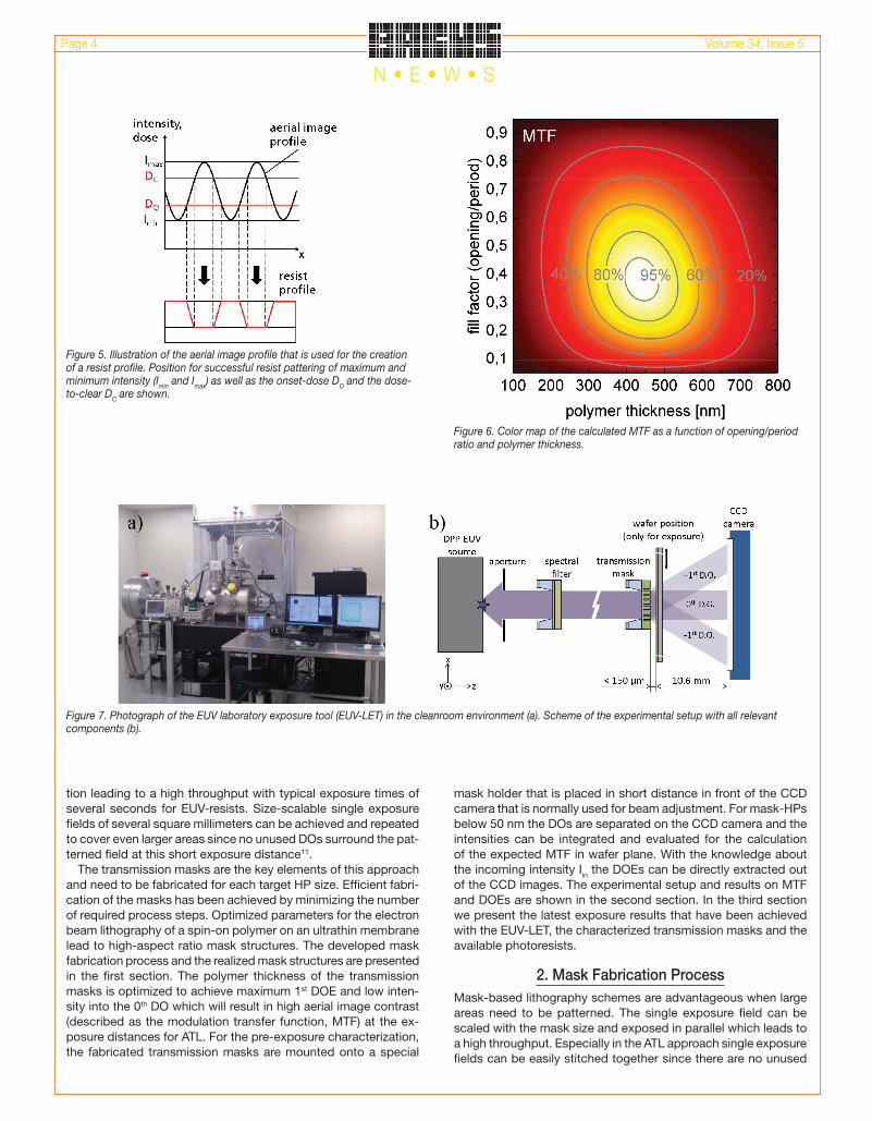
Figure 7. Photograph of the EUV laboratory exposure tool (EUV-LET) in the cleanroom environment (a). Scheme of the experimental setup with all relevant components (b).
Page 4 Volume 34, Issue 5
N • E • W • S

DOs surrounding the interference pattern. The width of the un-patterned area that surrounds the field is just depending on the bandwidth of the radiation that is used for exposure16. Interference effects can facilitate mask fabrication due to defect compensation and pattern demagnification but nevertheless masks need to be patterned with high-resolution structures on the nanoscale. This normally requires a transfer process from the patterned resist into the target material. The target material can either be a material that has a strong absorption in the EUV wavelength range like chromium (Cr), nickel (Ni) or tantalum nitride (TaN) or a material that has suitable phase-shifting properties like molybdenum (Mo)17, molybdenum nitride (MoN)18 or several polymers that are available
as spin-on EBL photoresists like polymethylmethacrylate (PMMA) or the 1:1 copolymer of a-chloromethacrylate and a-methylstyrene (ZEP520A, C13H15ClO2, density = 1.053 g/cm3)19,20. To avoid the pattern transfer we decided to use the EBL photoresist as a phase-shifting material. Since PMMA is not long-term-stable against EUV radiation21 and offers low contrast and sensitivity, we have used ZEP520A for the mask fabrication process.
We assume that for the ATL all DOs contribute to the intensity maxima of the aerial image and the intensity minima or background of the aerial image is defined mainly by the 0th DO. Achieving a minimal background or lowest intensity into the 0th DO will then lead to a maximized MTF. By optimizing the polymer thickness
Table 1. Overview of the measured DOEs and the expected MTFs at wafer plane for the investigated masks. As a reference the calculated values for an optimal line grating as calculated by [22] are given.
Figure 8. Photograph of CCD camera with attached mask holder and inserted transmission mask (a). CCD image of the diffraction pattern for 50-nm-HP mask at a mask-camera distance of 10.6 mm. At this distance the 1st DOs are clearly separated from the 0th DO. The 13 different regions of interest (ROIs) are outlined red and numbered (b).
Volume 34, Issue 5 Page 5
N • E • W • S

for a π-phase-shift between the directly transmitted beam and the shifted one that passes the polymer there is almost no inten-sity in the 0th DO (Fig 1a). The opening/period ratio of the mask structures also influences the intensity into 0th DO. The minimum 0th DO intensity can be achieved at a ratio of ~0.4 (or exactly 0.38 for 440 nm polymer thickness22) leading to the maximum MTF (Fig. 1b). Note that if only the 1st DOE needs to be maximized the polymer thickness needs to be slightly reduced from 440 nm to 404 nm leading to a phase-shift that is less than π to account for absorption. Additionally the opening/period ratio needs to be set to 0.5 22-24.
Suited materials for membranes are niobium (Nb), Mo, zirconium (Zr) and silicon nitride (SiNx) but only SiNx is commercially available as a membrane25. The here presented process is based on SiNx membranes with a thickness of 45 nm, measured with spectro-scopic ellipsometry (Sentech SE800) at four positions outside of the membrane area due to a low signal intensity on the membrane. At this thickness silicon-rich SiNx has a transmission of 47.5 % at 10.77 nm and 81.5 % at 13.50 nm23. Compared to our previously presented transmission mask fabrication process for amplitude masks (Ni-absorber on Nb-membrane) that consists of over 30 process steps26 this process is less complex and requires only an electron beam lithography (EBL) setup and a resist processing wet-bench. The process consists in total of four main process steps that lead to highly efficient phase-shifting masks (Fig. 2).
As a first step, the SiNx membrane sample (chip size 10 x 10 mm2, membrane size = 1 x 1 mm2) is dehydrated on a hotplate at 180 °C for 120 seconds. After a cool-down on the chill-plate for 120 seconds the sample is primed at a low pressure with gaseous hexamethyldisiloxane (HMDS) at a temperature of 130 °C. After a cool-down (120 s) the sample is placed off-centered on the vacuum chuck of the spin-coater to protect the SiNx-membrane during coating. After dispense of the photoresist (undiluted ZEP520A-7) the sample is spin-coated at a rotation speed between 2000 and 3000 rpm. The rotation speed is increased over the shelf-time of the resist to compensate the solvent evaporation and achieve a constant resist thickness of ~440 nm. After the resist coating the sample is prebaked at 180 °C for 240 s and cooled down on the
chill-plate (120 s).In the next step, the pattern is defined by EBL (Electron-Beam
Writer Vistec EBPG 5000plus). The patterning of the thick resist layer on top of the thin SiNx membrane is one of the main chal-lenges of this fabrication process because sub-50 nm structure sizes will result in aspect ratios greater than 8. Achieving these high aspect ratios requires optimal EBL parameters and an opti-mized layer system. With the help of a Monte Carlo simulation on the electron trajectories, the influence of the acceleration voltage and the substrate on the deposited energy around the electron injection point has been analyzed (Fig. 3).
The patterning on the membrane leads to a lower long range scattering (radius > 300 nm) for both acceleration voltages due to the absent backscattering in the substrate. The short range scattering (radius < 300 nm) is only reduced at higher accelera-tion voltages. Additionally higher acceleration voltages lead to a lower forward scattering in the 430 nm thick resist layer. Based on these simulations the EBL was performed on the membrane at an acceleration voltage of 100 kV with a beam current of 100 pA and a beam-step-size of 1 nm. For the investigated masks the layout consists of round openings in rectangular arrangement with an opening/period ratio of 0.4. Optimal dose values have been determined experimentally in a coarse dose-selection scan with a dose step of 100 μC/cm2. The determined dose window is relatively wide due to the low back- and forward scattering in this configuration. For the 50-, 40-, 30-nm-HP masks this resulted in optimal doses of 1400 to 1700 μC/cm2. These doses are higher than the standard EBL dose of ~100 μC/cm2 for ZEP520A due to the fact that the patterning of the relatively thick photoresist is done on a membrane (lower electron backscattering) with a high acceleration voltage (lower electron forward scattering) and that the samples are developed at 0 °C (lower resist sensitivity but higher contrast). For each mask an overall area of 1100 x 1100 μm2 has been patterned by EBL to cover the whole membrane area. The EBL patterning took between 12 and 16 hours for the investigated mask structures. An increase of the beam current or the beam step size has not been further analyzed but would result
Figure 9. Top-down close-up SEM images of the transmission mask structures (left side) and the therewith achieved resist structures in the exposure result at achromatic Talbot distance. Note that the pattern in the exposure result is tilted by 45° due to interference effects. Additionally the HP of the exposure result is reduced by a factor of √2 compared to the mask-HP (scale bar = 100 nm for all).
Page 6 Volume 34, Issue 5
N • E • W • S

in a reduced beam-on time.In the third step the samples are cold developed at a tempera-
ture of 0 °C (set temperature = -1 °C) for 90 s with the standard developer n-amyl acetate (ZED-N50). After this the samples are transferred into a first isopropanol (IPA) bath for development stop (30 s) and into a second IPA bath for further removal of the devel-oper residuals (also for 30 s). The remaining IPA is then evaporated on a hotplate at 55 °C. The IPA evaporation is done instead of the nitrogen blow-dry to avoid damage to the membrane and to reduce the influence of the capillary forces during drying27. Further reduction of the capillary forces can be achieved by applying a critical point drying technique28.
The fourth step of this fabrication method is the hard-bake of the photoresist at a temperature of 100 °C for 180 s. After a final cool-down for 120 s on the chill-plate the transmission masks are ready-to-use for EUV exposures.
For the top-down pattern inspection with scanning electron microscopy (Zeiss SEM Gemini 1550VP) it is necessary to deposit a thin (3 - 5 nm), conductive layer of iridium (Ir) onto the polymer layer. Otherwise an SEM inspection is not possible: low accelera-tion voltages (several kV) lead to a charging of the membrane area and higher acceleration voltages lead to a low signal-to-noise ratio due to low backscattering on the membrane. Cross-sectional images of the patterned polymer layer have been created with a dual beam setup consisting of a focused ion and an electron beam which are used for material deposition and imaging, cutting and polishing (FEI HELIOS Nanolab 600i Dualbeam). For the prepara-tion of the cross-sectional images a thick layer of platinum (Pt) has to be deposited on top of the resist structures. The top-down and cross-sectional images for the fabricated mask structures are shown in Fig. 4.
The sample preparation for the cross-sectional images consists of several process steps and is quite challenging since the resist layer tends to deform during preparation. It is also not clear if the resist thickness is reduced during the preparation procedure or already during EBL patterning of the structures. The thickness reduction is the largest in the densely patterned area of the resist. From the cross-sectional images one can identify slightly negative sidewalls due to the dominant forward scattering in the resist layer which seems to limit this process to mask HPs with a minimal size of 30 nm. For HPs below 30 nm one would need to change the process to other spin-on polymers or other phase-shift materials that allow for a lower layer thickness.
3. Diffraction Efficiencies and Aerial Image ContrastThe diffraction efficiency for transmission gratings can be calcu-lated if the exact geometry of the grating is known in terms of the actual bar thickness, the opening-to-period ratio and the cross-sectional shape. Additionally, the chemical composition of the grating material needs to be known to include the optical material constants (complex refractive index) into the calculation22,29-31. Although the calculated diffraction efficiency is independent of the grating period, in practice smaller periods lead to lower dif-fraction efficiencies since processing becomes more challenging and results in stronger deviations from the targeted shape. In the presented fabrication process a smaller period leads to a degrada-tion of the cross-sectional shape and the same is likely to occur if a process with a pattern transfer is employed. Also the exact chemical composition of the polymer after EBL, development, hard-bake and EUV exposures can change which can result in a change of the refractive index32. Additionally the total diffraction efficiency is influenced by the actual emission spectrum of the
source, especially if radiation with a certain bandwidth is used. For these reasons a more practical approach for the estimation of the diffraction efficiency is presented.
With the knowledge of the intensities into each DO and the incoming intensity Iin, the DOEs and the MTF of the aerial image profile can be calculated. By knowing the MTF in the wafer plane one can already conclude if the mask can be used for successful resist patterning. This is possible because the resist performance can be also determined experimentally by open-frame exposures and the plotted characteristic curve. Out of the characteristic curve the resist contrast (g-value) and the critical modulation transfer function (CMTF) can be extracted. Both are a function of the onset-dose DO and the dose-to-clear DC. The relationship between the resist performance and the MTF is schematically shown in Fig. 5. For a perfect photoresist DO and DC are equal, meaning that even the smallest MTF is sufficient for patterning. In reality a MTF > CMTF is required to produce a height profile in the resist (Fig. 5)6,33,34.
For Talbot lithography the minimal intensity of the aerial image profile can be defined as the intensity into the 0th DO as Imin = I0th. The maximal intensity Imax is then the sum of the intensities into the 0th DO and all other DOs and can be calculated as Imax = I0th + I1st +…+ In. The MTF can therefore be calculated as:
nstth
nst
IIIII
IIII
MTF+++
++=
+−
=...2
...
10
1
minmax
minmax )1( .
This calculated MTF can be understood as the maximal intensity modulation at the first Talbot distance and serves as a measure for the mask quality. The real MTF is further reduced at subsequent Talbot planes by the limited temporal and spatial coherence of the source35. The MTF calculated as a function of the opening/period ratio and the polymer thickness is shown in the color map (Fig. 6). For the calculation the intensities up to the 6th DOs are included.
For the calculation of the DOEs the intensities into the different DOs need to be compared to Iin. The absorption of the grating structure Agrating is defined as Agrating = Iin - I0th - I1st -…- In. Light that is scattered into larger angles or DOs is not included in this assumption. Therefore Agrating represents the upper limit for the absorption losses.
The fabricated transmission masks are characterized in the EUV-LET (Fig. 7 a). The experimental setup for the mask characterization consists of the DPP source, an aperture (diameter = 1 mm) for beam definition, a spectral filter (Nb (500 nm)/Si3N4 (10 nm)), the transmission mask to be characterized and the CCD camera for the detection of the DOs (Fig. 7 b). In the standard configuration15 for photoresist exposures a thinner spectral filter (Nb (100 nm)/ Si3N4 (10 nm)) is used and the wafer is positioned in a mask-wafer distance below 150 μm.
For this series of experiments the transmission mask is fixed in a special mask holder that is directly mounted onto the connec-tion flange of an EUV-sensitive back thinned CCD camera (Andor i-Kon M934, 1024 x 1024 pix2, 13 x 13 μm2) (Fig. 8 a). Thereby a mask-camera distance of 10.6 mm is realized where the DOs for a 50 nm mask HP with an area of 1 x 1 mm2 are separated by ~150 μm (for l = 10.77 nm). For all measurements the CCD and EUV source settings have been kept constant. The utilized EUV source is operated at a frequency of 100 Hz with a xenon (Xe) and argon (Ar) gas mixture14 of Xe/(Xe+Ar) = 8.3 %. The exposure time of the CCD camera is set to 150 μs and 10 single images are accumulated and corrected by dark images that are taken in the same manner (= 150 pulses/image). Dark signal is minimized by cooling-down the CCD chip to -40 °C for all measurements. For the
Volume 34, Issue 5 Page 7
N • E • W • S

measurements first a SiNx-membrane is fixed to the CCD-camera. This membrane belongs to the same batch that has been used for transmission mask fabrication and is used for the measurement of Iin. After this, the SiNx sample is replaced by a transmission mask. The CCD image that is recorded for the 50-nm-HP mask is shown in Fig. 8 b.
The CCD image provides information on the diffraction pattern that is generated by the grating structure. For image processing 13 different regions of interest (ROIs) have been defined as shown in Fig. 8 b. It shows the 0th DO (ROI #1) that is surrounded by the 1st DOs (ROI#2 to 5). If the scaling is adjusted it is also possible to identify the 1st DOs (ROI #6 to 9) that appear for the diagonal axis and also the 2nd DOs can be found (ROI #10 to 13) for some gratings. The 2nd DOs for the diagonal axis and higher DOs do not appear in the measurements. The DOs for the diagonal grating axis are only included in the calculation of the MTF and absorp-tion. The position of the ROIs is slightly adjusted for masks with smaller HPs and the number of counts are integrated in each ROI and correspond to the intensity into this DO. For the determination of the 0th DOE the integrated counts into the 0th DO are compared to Iin (integrated counts of SiNx membrane measurement). The 1st DOE is calculated by comparing the counts of the 1st DOs (ROI#2 to 5) with the Iin and the same for higher DOs. The results of these measurements for the investigated masks are summarized in table 1 and compared to an optimal mask with a polymer thickness of 440 nm with an opening/period ratio of 0.38 (Fig. 6) which can lead to a theoretically achievable MTF of 100 %.
In a first experiment, the transmission masks with three differ-ent HPs were tested directly after fabrication. For the 50-nm-HP almost 42 % of Iin is in the 1st DOs, only 14 % is in the 0th DO. For all masks there is less than 1.5 % of Iin in the 2nd and higher DOs. For the 40-nm-HP the intensity in the 0th DO increases by 10 % and is reduced by the same amount in the 1st DOs. Thereby the absorption of the mask is almost constant since the opening/period ratio is same for these masks due to good pattern quality. Already by SEM/FIB inspection a lower pattern quality has been observed for the 30-nm-HP mask (Fig. 4b) which results in a strong reduction of MTF to ~11 %. To check the stability of the polymer against EUV radiation, an already exposed 40-nm-HP mask was inspected with no indication of radiation damage after a total exposure dose of 2 J/cm2. An additional mask was fabricated where the EBL dose was increased by 20 % in comparison to the optimal EBL dose. This results in slightly larger openings but the effect on the MTF is small (~3 % reduction) since the patterning is done on the membrane and the EBL dose window is wide. The absorption is almost similar for the 50- and 40-nm-HP masks meaning that the Imax has to be also similar for these two masks. For resist pattern-ing this would result in a similar dose-to-size for the different HPs which is advantageous. Achieved high MTF values of up to 63.7 % allow for flexible patterning also of low contrast photoresists.
By taking into account the measured values for the DOEs the effective polymer thickness and opening/period ratio can be calculated (2nd column in tab. 1). The calculations show that the effective thickness is reduced down to 200 nm for the HP of 30 nm. A thickness reduction can also be observed in the cross-sectional SEM images (Fig. 4 b-c) which is larger for smaller half-pitches. One needs to note, that for all calculations a rectangular cross-section is assumed. This is definitely not the case for the 30-nm-HP where the non-rectangular shape degrades the DOEs. The calculated effective polymer thickness doesn’t take the shape change into account which leads to an underestimation of its value. The MTF that can be experimentally used for resist patterning might be
further reduced by positioning system instabilities, thermal drift or vibrations between the mask and the wafer.
4. EUV ExposuresThe characterized masks have been used for exposure series in the EUV-LET to create a height profile in a photoresist. For the exposures we used a high-sensitivity chemically amplified EUV resist with identical pre- and post-exposure processing as in our previous investigations for the analysis of the process window at 50 nm wafer HP15. The resist thickness has been measured by spectroscopic ellipsometry (Sentech SE800) to be 37 nm and the dose-to-clear at awavelength of 10.77 nm is 14 mJ/cm2. The shown exposure results are achieved at a mask-wafer distance <20 μm and an exposure dose of 17 mJ/cm2 leading to exposure times of less than 90 s (Fig. 8).
The mask-HPs are reduced by a factor of √2 (and tilted by 45°) in the exposure result leading to 35 and 28 nm wafer HPs which is to our knowledge the record resolution for ATL. So far the exposure results for the 30-nm-HP mask led to a modulation of 21 nm HP in the exposure result which is reasoned by the lower MTF that is not matching the resist performance of our test EUV resist. To approach the theoretical resolution limit of 10 nm HP34 or even l/4 further hardware upgrades, mask optimizations and access to high-contrast resists are necessary.
Especially for sub-40 nm mask HPs we can already observe a pattern demagnification at the mask-wafer contact point for the utilized emission spectrum and transmission masks15. This dis-tance has been determined experimentally out of the diffraction pattern to be ~8 μm. This seems to be the minimal mask-wafer distance achievable in practice due to limited positioning accuracy and mask surface imperfections.
5. ConclusionsIn this paper we presented a four-step mask fabrication process that is based on thin SiNx-membranes with a spin-on polymer. This process allows to produce high-efficient phase-shifting masks within short processing time that are perfectly suited for the achro-matic Talbot approach. The simple and robust fabrication process has been scaled down to 30 nm mask HP. With on-membrane 100kV EBL patterning high aspect ratios and large EBL dose windows have been achieved that lead to a high reproducibility for the mask fabrication process. Furthermore the masks are stable against incoming EUV radiation.
For the characterization of the transmission masks we es-tablished an in-tool inspection method within the EUV-LET. By measuring the intensities into the DOs and comparing these to the incoming intensity the DOEs and the maximal MTF for each mask can be estimated. With this method transmission masks can be in-spected for long-term radiation stability and pattern quality. For this experimental method of DOE determination no exact knowledge of material composition or mask geometry (thickness, shape and opening/period ratio) is needed. The structure period can be easily extracted out of measurements. The inspection of the fabricated phase-shifting transmission masks resulted in 1st DOEs up to 42 % and 36 % for 50 nm and 40 nm HP respectively. For all masks the aspect ratio is in the range of six to seven. The absorption of these masks is below 40 % which leads to comparable through-put for all HPs (almost same dose-to-size). The crosssection of the 30-nm-HP mask shows negative sidewall angles and further reduced polymer thickness leading to a 1st DOE of 10 %.
The maximal MTF of almost 64 % is measured for the fabricated mask HP of 50 nm, for 40 nm HP it is still 45 % and drops down
Page 8 Volume 34, Issue 5
N • E • W • S

to 11 % for the 30 nm mask HP which is still sufficient for the patterning of high-contrast photoresists. By matching the polymer thickness to a π-phase-shift the 0th DO can be suppressed even more leading to higher MTF and throughput. The presented mask fabrication process can be pushed to MTF values of >90 % by matching the polymer thickness and the opening/period ratio of the fabricated masks to the optimal values.
The exposure results demonstrate the great potential of the exposure tool and the developed transmission mask technology. With the available EUV resists, the patterning of nanostructures down to 28 nm HP are shown. The further optimization of the mask fabrication process will lead to larger MTFs for smaller HPs and therefore more relaxed requirements on resist contrast.
6. AcknowledgementsThe authors would like to thank the cleanroom staff of the Helmholtz Nanoelectronic Facility at the Research Center Julich, Germany37. Especially we would like to acknowledge the work of Dr. Stefan Trellenkamp for the EBL of the fabricated transmis-sion masks and Dr. Elmar Neumann for the preparation of the cross-sectional SEM images. L. Juschkin acknowledges financial support from the Helmholtz Association for a Helmholtz Profes-sorship as a part of the Initiative and Networking Fund. This work was realized by cooperation activities in the frame of the Julich Aachen Research Alliance for Fundamentals of Future Information Technology (JARA-FIT).
7. References [1] Kim, S. Y., Nunns, A., Gwyther, J., Davis, R. L., Manners, I., Chaikin,
P. M. and Register, A., “Large-area nanosquare arrays from shear-aligned block copolymer thin films,” Nano Lett. 14, 5698-5705 (2014).
[2] Kayes, B. M., Filler, M. A., Putnam, M. C., Kelzenberg, M. D., Lewis, N. S. and Atwater, H. A., “Growth of vertically aligned Si wire arrays over large areas (>1cm2) with Au and Cu catalysts,” Appl. Phys. Lett. 91, 103110 (2007).
[3] Yang, X. M., Xiao, S., Wu, W., Xu, Y., Mountfield, K., Rottmayer, R., Lee, K., Kuo, D. and Weller, D., “Challenges in 1 Teradot/in.2 dot patterning using electron beam lithography for bit-patterned media,” J. Vac. Sci. Technol. B 25(6), 2202 (2007).
[4] Ekinci, Y., Vockenhuber, M., Terhalle, B., Hojeij, M., Wang, L. and Younkin, T. R., “Evaluation of resist performance with EUV interference lithography for sub-22 nm patterning,” Proc. of SPIE Vol. 8322, (11pp) (2012).
[5] Brose, S., Danylyuk, S., Tempeler, J., Kim, H., Loosen, P. and Juschkin, L., “Enabling laboratory EUV research with a compact exposure tool,” Proc. of SPIE Vol. 9776, (17pp) (2016).
[6] Wake, R. W. and Flanigan, M. C., “A review of contrast in positive photoresists,” Proc. SPIE Vol 539, Advances in Resist Technology and Processing II, 291-298 (1985).
[7] Shin, J., Han, G. and Ma, Y., “Resist line edge roughness and aerial image contrast,” J. Vac. Sci. Technol. B 19(6), (2001).
[8] Sanchez, M. I., Hinsberg, W. D., Houle, F. A. and Hoffnagel, J. A., “Aerial image contrast using interferometric lithography: effect on line-edge roughness,” Proc. of SPIE Vol. 3678, 0277-786 (1999).
[9] Seo, J. H., Park, J., Zhao, D., Yang, H., Zhou, W., Ju, B. K. and Ma, Z., “Large-area printed broadband membrane reflectors by laser interference lithography,” IEEE Photonics Journal 5(1), (2013).
[10] Lohmann, A. W. and Thomas, J. A., “Making an array illuminator based on the Talbot effect,” Applied Optics 29, 4337-4340 (1990).
[11] Kim, H., Li, W., Marconi, M. C., Brocklesby, W. S., and Juschkin, L., “Restorative self-image of rough line grids: application to coherent EUV Talbot lithography,” IEEE Photon. J. 8 (3), 2600209 (2016).
[12] Solak, H. H. and Ekinci, Y., “Achromatic spatial frequency multiplication: A method for production of nanometer-scale periodic structures,” J. Vac. Sci. Technol. B 23(6), 2705-2710 (2005).
[13] Benk, M. and Bergmann, K., “Brilliance scaling of discharge sources for extreme-ultraviolet and soft x-ray radiation for metrology applications,” J. Micro/Nanolith. MEMS MOEMS 11(2), 021106 (7pp) (2012).
[14] Bergmann, K., Danylyuk, S. V., and Juschkin, L., “Optimization of a gas discharge plasma source for extreme ultraviolet interference lithography at a wavelength of 11 nm,” J. Appl. Phys. 106, 073309 (2009).
[15] Brose, S., Tempeler, J., Danylyuk, S., Loosen, P. and Juschkin, L., “Achromatic Talbot lithography with partially coherent extreme ultraviolet radiation: process window analysis,” J. Micro/Nanolith. MEMS MOEMS 15(4), 043502 (2016).
[16] Karim, W., Tschupp, S. A., Oezaslan, M., Schmidt, T. J., Gobrecht, J., van Bokhoven, J. A. and Ekinci, Y., “High-resolution and large-area nanoparticle arrays using EUV interference lithography,” Nanoscale 7(16), 7386-7393 (2015).
[17] Saidani, M. and Solak, H. H., “High diffraction-efficiency molybdenum gratings for EUV lithography” Microelectronic Engineering 86, 483-485 (2009).
[18] Wang, L., Kirk, E., Wäckerlin, C., Schneider, C. W., Hojeij, Gobrecht, J. and Ekinci, Y., “Nearly amorphous Mo-N gratings for ultimate resolution in extreme ultraviolet interference lithography,” Nanotechnology 25, 235305 (7pp) (2014).
[19] Resnick, D. J., Dauksher, W. J., Mancini, D., Nordquist, K. J., Ainley, E., Gehoski, K. and Baker, J. H., “High resolution templates for step and flash imprint lithography,” J. Micro/Nanolith. MEMS MOEMS 1(3), 284–289 (2002).
[20] ZEON Chemicals, “ZEP520A Technical Report,” https://www.zeonchemicals.com/pdfs/ZEP520A.pdf, (valid by 2017).
[21] Eve, S. and Mohr, J., “Study of the surface modification of the PMMA by UV-radiation,” Procedia Engineering 1, 237-240 (2009).
[22] Schnopper, H.W., Van Speybroeck, L. P., Delvaille, J. P., Epstein, A., Källne, E., Bachrach, R. Z., Dijkstra, J. and Lantward, L., “Diffraction grating transmission efficiencies for XUV and soft x-rays,” Appl. Opt. 16, 1088 (1977).
[23] Henke, B. L., Gullikson, E. M. and Davis, J. C., “X-ray interactions: photoabsorption, scattering, transmission, and reflection at E=50-30000 eV, Z=1-92,” Atomic Data and Nuclear Data Tables 54(2), 181-342 (1993).
[24] Paivanranta, B., Langner, A., Kirk, E., David, C. and Ekinci, Y., “Sub-10 nm patterning using EUV interference lithography,” Nanotechnology 22, 375302 (7pp) (2011).
[25] Silson Ltd., www.silson.com (valid by 2017).
[26] Brose, S., Danylyuk, S. V., Juschkin, L. , Dittberner, C. , Bergmann, K., Moers, J., Panaitov, G., Trellenkamp, S. , Loosen, P. and Grutzmacher, D., “Broadband transmission masks, gratings and filters for extreme ultraviolet and soft X-ray lithography,” Thin Solid Films 520, 5080-5085 (2012).
[27] Raccurt, O., Tardif, F., Arnaud d’Avitaya, F. and Vareine, T., “Influence of liquid surface tension on stiction of SOI MOEMS,” J. Micromech. Microeng. 14, 1083-1090 (2004).
[28] Chang, S. W., Chuang, V. P., Boles, S. T., Ross, C. A. and Thompson, C. V., “Densely packed arrays of ultrahigh-aspect-ratio silicon nanowires fabricated using block-copolymer lithography and metal-assisted etching,” Adv. Funct. Mater. 19, 2495-2500 (2009).
Volume 34, Issue 5 Page 9
N • E • W • S

[29] Bräuninger, H., Predehl, P. and K. P., Beuermann, “Transmission grating efficiencies for wavelength between 5.4A and 44.8A,” Applied Optics 18(3), (1979).
[30] Braig, C., Predehl, P. and Kley, E. B., “Efficient extreme ultraviolet transmission gratings for plasma diagnostics,” Optical Engineering 50(6), 066501 (2011).
[31] Liu, Z., Shi, L., Pu, T., Li, H., Niu, J., Wang, G. and Xie, C., “Two-dimensional gratings of hexagonal holes for high order diffraction suppression,” Optics Express 25(2), 1339 (2017).
[32] Assaid, I., Hardy, I. and Bosc, D., “Controlled refractive index of photosensitive polymer: towards photoinduced waveguide for near infrared wavelengths,” Optics Communications 214, 171-175 (2002).
[33] Thompson, L. F., Wilson, C. G. and Bowden, M. J., [Introduction to Microlithography, 2nd Edition], American Chemical Society, 69f (1994).
[34] Plummer, J. D., Deal, M. and Griffin, P. D., [Silicon VLSI Technology: Fundamentals, Practice, and Modeling], Prentice Hall, New Jersey, 227-228 (2000).
[35] Patorski, K., “The self-imaging phenomenon and its application,” Progress in Optics 27, North Holland, Amsterdam, 34-39 (1989).
[36] Danylyuk, S., Loosen, P., Bergmann, K., Kim, H. and Juschkin, J., “Scalability limits of Talbot lithography with plasma-based extreme ultraviolet sources,” J. Micro/Nanolith. MEMS MOEMS 12(3), 033002 (7pp)(2013).
[37] Forschungszentrum Julich GmbH, “HNF - Helmholtz Nano Facility,” Journal of large-scale research facilities 3, A112 (2017).
Page 10 Volume 34, Issue 5
N • E • W • S

N • E • W • S
Sponsorship OpportunitiesSign up now for the best sponsorship
opportunities
Photomask 2018 — Contact: Melissa Farlow,
Tel: +1 360 685 5596; [email protected]
Advanced Lithography 2018 — Contact: Teresa Roles-Meier,
Tel: +1 360 685 5445; [email protected]
Advertise in the BACUS News!
The BACUS Newsletter is the premier publication serving the photomask industry. For information on how to advertise, contact:
Melissa Farlow, Tel: +1 360 685 5596 [email protected]
BACUS Corporate Members
Acuphase Inc.American Coating Technologies LLCAMETEK Precitech, Inc.Berliner Glas KGaA Herbert Kubatz
GmbH & Co.FUJIFILM Electronic Materials U.S.A., Inc.Gudeng Precision Industrial Co., Ltd.Halocarbon ProductsHamaTech APE GmbH & Co. KGHitachi High Technologies America, Inc.JEOL USA Inc.Mentor Graphics Corp.Molecular Imprints, Inc.Panavision Federal Systems, LLCProfilocolore SrlRaytheon ELCAN Optical TechnologiesXYALIS
■ Photomask Sales Surge
Dylan McGrathSales of semiconductor photomasks surged to a record $3.75 billion last year and are expected to top $4 billion in 2019, according to the SEMI trade group.SEMI (Milpitas, Calif.) estimated mask sales surged by 13 percent last year, driven by continued growth in manufacturing in the Asia-Pacific region and an increase in the number of designs at 45nm and below. Mask sales are projected to grow by 5 percent this year and an additional 4 percent next year, SEMI said.Taiwan was the largest market for photomasks for the seventh consecutive year in 2017 and is expected to remain No. 1 through 2019, according to SEMI’s forecast, while South Korea is now the No. 2 market for masks. https://www.eetimes.com/document.asp?doc_id=1333168
■ SEMI reports 2017 global semiconductor equipment sales of $56.6 billion
Korea claimed the largest market for new semiconductor equipment for the first time, shattering all previous regional spending records with USD 17.95 billion in equipment sales. Taiwan fell to the second position with sales of USD 11.49 billion. Annual spending rates increased for South Korea, Europe, China, Japan and North America. However, new equipment markets in Taiwan and Rest of World (primarily Southeast Asia) contracted. http://evertiq.com/news/43882
■ Trump Presses China to Buy More U.S. Chips
Dylan McGrathChina is considering buying more semiconductors from U.S. firms as part of behind-the-scenes negotiations to reduce the U.S. trade deficit with China and avert a trade war, according to reports. https://www.eetimes.com/document.asp?doc_id=1333125
■ Semiconductor Industry Rattled by Trade War Fears
Sejuti Banerjea The semiconductor industry is dependent on China, both on the production and especially on the sales side because of the rapid pace of technological progress in the country. China today imports 29% of its semiconductors from overseas suppliers (a large percentage of which are American) and the government has the stated goal of reducing that dependence in the near future. It has a comprehensive plan (5-year plans, actually) in place to gradually produce more chips within the country, for which it has devoted considerable resources.There is concern among chip makers that the Chinese will produce in the not-too-distant future enough to create an oversupply situation that will lower prices across the industry.
■ GloFo reaches for the automotive semiconductor market
Christoph HammerschmidtFollowing a comprehensive audit by TuV Sud, Globalfoundries’ Dresden-based Fab 1 plant has received the certification required to produce components for the automotive industry. In the first place, the company plans to leverage its 22FDX process as the vehicle to conquer the booming market for automotive sensors and processors.More News: SUSS GlueBuster system dramatically reduces the volume and cost of chemicals used in the pellicle glue removal process. http://markets.businessinsider.com/news/stocks/suss-microtec-extends-photomask-equipment-offering-with-masktrack-gluebuster-1020952905
■ GLOBALFOUNDRIES and Toppan Photomasks Extend Advanced Photomask Joint Venture in Germany
https://www.globalfoundries.com/news-events/press-releases/globalfoundries-and-toppan-photomasks-extend-advanced-photomask-joint-venture-in-germany
■ Foundry War: Samsung Electronics Aims to Overtake TSMC by Developing 7-nm Foundry Process
http://www.businesskorea.co.kr/english/news/ict/21486-foundry-war-samsung-electronics-aims-overtake-tsmc-developing-7-nm-foundry-process
■ ASML: Arms Dealer in Epic Battle of Taiwan Semi vs. Samsung, Says Credit Suisse
https://www.barrons.com/articles/asml-arms-dealer-in-epic-battle-of-taiwan-semi-vs-samsung-says-credit-suisse-1523291624
Volume 34, Issue 5 Page 11
N • E • W • S Industry Briefs

SPIE is the international society for optics and photonics, an educational not-for-profit organization founded in 1955 to advance light-based science, engineering, and technology. The Society serves nearly 264,000 constituents from 166 countries, offering conferences and their published proceedings, continuing education, books, journals, and the SPIE Digital Library in support of interdisciplinary information exchange, professional networking, and patent precedent. SPIE provided more than $4 million in support of education and outreach programs in 2017. www.spie.org
International HeadquartersP.O. Box 10, Bellingham, WA 98227-0010 USA Tel: +1 360 676 3290 Fax: +1 360 647 [email protected] • www.SPIE.org
Shipping Address1000 20th St., Bellingham, WA 98225-6705 USA
Managed by SPIE Europe 2 Alexandra Gate, Ffordd Pengam, Cardiff, CF24 2SA, UK Tel: +44 29 2089 4747 Fax: +44 29 2089 [email protected] • www.spieeurope.org
2018
SPIE Photomask Technology + EUV Lithography17-20 September 2018Monterey Convention Center Monterey, California www.spie.org/puv
The 34 European Mask and Lithography Conference, EMLC 201819-20 June 2018MINATEC Conference CentreGrenoble, Francewww.emlc-conference.com
Corporate Membership Benefits include:■ 3-10 Voting Members in the SPIE General Membership,
depending on tier level
■ Subscription to BACUS News (monthly)
■ One online SPIE Journal Subscription
■ Listed as a Corporate Member in the BACUS Monthly Newsletter www.spie.org/bacushome
C A L E N D A R
About the BACUS GroupFounded in 1980 by a group of chrome blank users wanting a single voice to interact with suppliers, BACUS has grown to become the largest and most widely known forum for the exchange of technical information of interest to photomask and reticle makers. BACUS joined SPIE in January of 1991 to expand the exchange of information with mask makers around the world.
The group sponsors an informative monthly meeting and newsletter, BACUS News. The BACUS annual Photomask Technology Symposium covers photomask technology, photomask processes, lithography, materials and resists, phase shift masks, inspection and repair, metrology, and quality and manufacturing management.
Individual Membership Benefits include:■ Subscription to BACUS News (monthly)
■ Eligibility to hold office on BACUS Steering Committee
www.spie.org/bacushome
You are invited to submit events of interest for this calendar. Please send to [email protected]; alternatively,
email or fax to SPIE.
h
h
Join the premier professional organization for mask makers and mask users!
Page 12 Volume 34, Issue 5
N • E • W • S