optimization of the two stage process for cu(in,ga)se 2
TRANSCRIPT

University of South FloridaScholar Commons
Graduate Theses and Dissertations Graduate School
7-8-2004
Optimization Of The Two Stage Process ForCu(In,Ga)Se2 Solar CellsShirish PetheUniversity of South Florida
Follow this and additional works at: https://scholarcommons.usf.edu/etdPart of the American Studies Commons
This Thesis is brought to you for free and open access by the Graduate School at Scholar Commons. It has been accepted for inclusion in GraduateTheses and Dissertations by an authorized administrator of Scholar Commons. For more information, please contact [email protected].
Scholar Commons CitationPethe, Shirish, "Optimization Of The Two Stage Process For Cu(In,Ga)Se2 Solar Cells" (2004). Graduate Theses and Dissertations.https://scholarcommons.usf.edu/etd/1194

Optimization Of The Two Stage Process For Cu(In,Ga)Se2 Solar Cells
By
Shirish Pethe
A thesis submitted in partial fulfillment of the requirement for the degree of
Master of Science in Electrical Engineering Department of Electrical Engineering
College of Engineering University of South Florida
Major Professor: Don L. Morel, Ph.D. Christos Ferekides, Ph.D.
Y.L.Chiou, Ph.D.
Date of Approval: July 8, 2004
Keywords: cigs, photovoltaics, absorber layer, co-evaporation, cis
© Copyright 2004, Shirish Pethe

ACKNOWLEDGMENTS
I would like to thank my major professor Dr. Don Morel for giving me an
opportunity to work on this project and also for his valuable guidance during the course
of this research. I would also like to thank Dr. Chris Ferekides for agreeing to be on my
committee and helping me in the lab whenever I faced problems. Also like to thank Dr.
Chiou for being on my committee and for his guidance.
I am also thankful to Mike and Trunk from the Electrical Engineering department
for their timely help in all my problems. I would also like to thank the machine shop
guys, Bob and others.
I would like to thank my colleagues, Harish, Venkatesh, and others in the lab that
were always there to help me and made working in the lab a wonderful experience. I
would also like to thank my friends at USF that were always there to support me and
made my stay at USF a memorable one.
Last but not the least I would like to thank my family and friends back in India for
their constant encouragement and support without which I would not be here.

i
TABLE OF CONTENTS
LIST OF TABLES iii
LIST OF FIGURE iv
ABSTRACT vi
CHAPTER 1 INTRODUCTION 1
1.1 Need for Solar Energy 1
1.2 Thin Film Solar Cells 2
1.3 CIS Thin Film Technology 3
1.4 CIGS Thin Film Technology 5
CHAPTER 2 SEMICONDUCTOR AND SOLAR CELL PHYSICS 8
2.1 Introduction 8
2.2 P-N Junctions 10
2.3 Heterojunctions 14
2.4 Solar cells 16
CHAPTER 3 DEVICE FABRICATION AND CHARACTERIZATION 20
3.1 Device Structure 20
3.1.1 Substrate 21
3.1.2 Back Contact 21
3.1.3 Cadmium Sulfide 22
3.1.4 Front Contact 23
3.2 Device Fabrication 24
3.2.1 Back Contact Deposition 24
3.2.2 Absorber Layer Deposition 25

ii
3.2.2.1 Type I Precursors 26
3.2.2.2 Type V Precursors 28
3.2.3 Window Layer Deposition 30
3.2.5 Front Contact Deposition 30
3.3 Device Characterization 30
CHAPTER 4 RESULTS AND DISCUSSION 32
4.1 Effect of Bulk Copper 32
4.2 Effect of Venting on Jsc 34
4.3 Type V Precursors 36
4.3.1 Effect of Ga Content on Device Performance 37
4.3.2 Effect of Substrate Temperature 39
4.3.3 Effect of Selenization on Device Performance 40
4.3.4 Effect of Venting on Voc 42
4.4 ZnSe Buffer Layer 45
4.5 Effect of Silicon Nitride Layer 45
CHAPTER 5 CONCLUSIONS AND RECOMMENDATIONS 47
REFERENCES 50

iii
LIST OF TABLES Table 4.1 Effect of Cu Thickness on Device Performance 33
Table 4.2 Overall Device Performance 34
Table 4.3 Device Performance With Respect to Run Sequence 40
Table 4.4 Overall Device Performance for Si3N4 Thickness Variation 46

iv
List Of Figures Figure 1.1 Chronological Evolution of Small Area Solar Efficiencies 2
Figure 1.2 A Ternary Cu-In-Se Phase Diagram 4
Figure 1.3 Chalcopyrite Structure of CIGS 5
Figure 1.4 Change in Bandgap as Function of Ga Content 6
Figure 2.1 Simplified Band Diagram of Semiconductor 10
Figure 2.2 Space Charge Distribution 11
Figure 2.3 Electric Field and Potential Distribution 12
Figure 2.4 Band Bending in P-N Junction 13
Figure 2.5 Energy Band Diagram of Isolated Semiconductor 15
Figure 2.6 Energy Band Diagram of Heterojunction 15
Figure 2.7 Ideal I-V Curve of Solar Cell 16
Figure 2.8 Energy Band Diagram of Solar Cell under Illumination 17
Figure 2.9 Equivalent Circuit of Solar Cell 18
Figure 2.10 Effect of Series and Shunt Resistances 19
Figure 3.1 Basic Structure of CIGS Solar Cell 20
Figure 3.2 Wurtzite Structure of CdS 22
Figure 3.3 Source Arrangement for Type I Precursors 26
Figure 3.4 Temperature Profile of Selenization for Type I Precursors 27
Figure 3.5 Source Arrangement for Type V Precursors 28
Figure 3.6 Temperature Profile of Selenization for Type I Precursors 29
Figure 4.1 Voc Distribution in Run P044, P049, P059 33
Figure 4.2 Spectral Response for P007, P008 and H299 34
Figure 4.3 Voc and Fill Factor Distribution for P056 35
Figure 4.4 I-V Characteristics of Device P056-11 36
Figure 4.5 Spectral Response for P056 and P065 37
Figure 4.6 Voc Distribution for Ga Content 38

v
Figure 4.7 Voc Distribution for Sample P071 39
Figure 4.8 Spectral Responses for Samples P068 and P071 40
Figure 4.9 Voc Distribution for Samples P071 and P072 41
Figure 4.10 Voc Distribution for Samples P067 and P069 41
Figure 4.11 Voc Distribution for Samples P065, P066 and P069 43
Figure 4.12 Bandgap Shift for Run Sequence 43
Figure 4.13 I-V Characteristics of Device P072-08 44
Figure 4.14 Voc Distribution for Sample P007 45

vi
OPTIMIZATION OF THE TWO STAGE PROCESS FOR Cu(In,Ga)Se2 SOLAR CELLS
Shirish Pethe
ABSTRACT
Copper Indium Gallium DiSelenide absorber layers are fabricated using a two stage
manufacturing friendly process. The first step involves the sequential deposition of
Copper and Gallium and co-deposition of indium and selenium at 275oC. This is followed
by the second stage where the substrate is annealed in the presence of Selenium and a
thin layer of copper is deposited to neutralize the excess Indium and Gallium on the
surface to form the CIGS absorber layer. The top copper thickness as well as the time of
deposition was varied to study the effect of Copper on the performance of the cells.
Another recipe was developed for the precursor formation, where Gallium was
co-evaporated with Indium and Selenium. A large bandgap shift was seen with this recipe
and the open circuit voltage was increased.
The performance of CIGS/CdS/ZnO solar cells thus fabricated was characterized
using techniques like I-V, C-V, Spectral Response and EDS/SEM. Cells with open circuit
voltages of 420-450 mV, short circuit currents of 33-38 mA/cm2, fill factors of 58-62%
and efficiencies of 9-11% were routinely fabricated.

1
CHAPTER 1
INTRODUCTION
1.1 Need For Solar Energy
Development of clean energy resources as an alternative to fossil fuels has
become one of the important challenges for modern science and technology in the 21st
century. Reduction of air pollution and preservation of the ecological systems of earth are
the main motivation factors behind these huge efforts.
Some of the major contenders for the alternative clean resources are hydroelectric,
tidal, nuclear and solar energy. But of all these renewable energy sources photovoltaic is
the most promising one as a future energy technology. The photovoltaic effect is the
process of direct conversion of sunlight into electrical energy. This effect was first
observed by Henri Becquerel in 1839. The major advantage of these photovoltaic systems
is that they tap an almost inexhaustible resource that is free of charge and available
everywhere in the world. Even though the photovoltaic effect was first observed in 1839,
the first practical cell was developed by Chapin et.al at Bell Labs in 1954. [1]
1.2 Thin Film Solar Cells
The main barrier impeding the expansion of the terrestrial application of
photovoltaic is the high price of the solar cell modules. The reasons for these high costs
are the high processing and material costs. A recent survey suggests that a further cost

2
reduction to one fifth of the present level is a must for photovoltaics to match the
conventional electricity price. One of the solutions to achieve a reduction in this cost is
the development of thin film solar cells. This cost reduction is due to factors like lower
material use, fewer and simpler processing steps as compared to a traditional wafer based
crystalline silicon solar cell.
The thin film technologies use simpler device processing techniques like
evaporation, sputtering, etc. for large area modules and arrays. The designs of most thin
film technologies have common processing techniques so the manufacturing costs are
very similar. Hence, the choice of any technology is based on the factors like highest
achievable conversion efficiency, reliability, availability of materials and environmental
concerns. At present, research is done on the alloys of amorphous Silicon, CdTe, and CIS
as major contenders for large scale production. Figure 1.1 [2] shows the chronological
evolution of small area solar cell efficiencies in these three technologies.
Figure 1.1 Chronological Evolutions of Small Area Solar Efficiencies

3
1.3 CIS Thin Film Technology
CuInSe2 (CIS) is a ternary alloy belonging to the I-III-VI2 compound
semiconductor group. Its lattice elements are tetrahedrally coordinated like all adamanite
semiconductors. CIS has a bandgap of 1.0 eV and one of the highest reported absorption
coefficient of 3.6E5 cm-1[3]. The properties of CIS strongly depend on its composition,
and the doping of CIS is controlled by the intrinsic defects. Hence, we have either p-type
or n-type CIS if the material is grown Cu-poor and p-type if Cu-rich film is grown. The
Cu-rich films are highly conductive due to acceptor defects (copper atoms on indium
sites). The n-type In-rich films are highly resistive due to the donor defects (indium on
copper sites) and acceptor defects (copper vacancies) occurring at the same time. Some of
the recent studies have observed a thin surface layer of CuIn3Se5. This is termed as the
ordered vacancy compound (OVC), a defect chalcopyrite which is slightly In rich [4].
The OVC has a bandgap of 1.3 eV. As compared to binary compounds the ternary
compound CIS is more tolerant to small deviations from stoichiometry. The composition
needs to be slightly In rich in order to achieve good device performance. As the metal
ratio (I/III) approaches unity the carrier concentration increases which results in better
cell performance. This could be attributed to the formation of Cu2Se grains. This
behavior is explained based on the Cu-In-Se ternary phase diagram [5] shown in figure
1.2. In Se rich films, both Cu and In vacancies yield strongly p-type films. Simultaneous
formation of oppositely charged defects in the In rich films may lead to a highly
compensated, highly resistive n or p-type films.

4
Figure 1.2 A Ternary Cu-In-Se Phase Diagram
The first thin film CIS solar cell was produced by the evaporation of CIS as a
compound [6]. CIS films can be produced by co-evaporation or sequential evaporation of
elemental sources. In co-evaporated CIS films, the composition of the materials with
regard to the metal ratios corresponds to the evaporation rates whereas in sequentially
evaporated CIS films, it corresponds to the thickness. Co-evaporation of the elemental
sources gives better device quality films as compared to sequentially evaporated films.
But for commercial purposes sequential evaporation is preferred over co-evaporation
because it requires lesser control over the evaporation rates. Some of the other techniques
being researched for deposition of CIS films are electro deposition, screen printing,
particle deposition, sputtering, MBE, and MOCVD.

5
1.4 CIGS Thin Film Solar Cells
If the bandgap of the thin film solar cell is increased it increases the band-bending
which causes an increase in the open circuit voltage (Voc) but also decreases the short
circuit current (Jsc) as fewer photons are absorbed in the long wavelength range and so
fewer carriers are generated. Thus there is a current-voltage tradeoff. If the bandgap of
the absorber layer is increased, the doping of the window layer which is ZnO can be
increased to reduce the resistive losses without the problem of free carrier absorption, as
current is no longer generated in the infrared region. This bandgap increase can be caused
by alloying a quaternary compound of Cu (In,Ga)Se2 (CIGS). The chalcopyrite structure
of the CIGS compound is shown in figure 1.3. This is done by alloying CIS and CGS. As
the bandgap of CGS (1.7 eV) is higher than that of CIS (1.0 eV) we get a bandgap
increase.
Figure 1.3 Chalcopyrite Structure of CIGS

6
The bandgap of the composition Cu In1-xGaxSe2 is given by [7]
xEg 71369.00032.1 += (1.1)
The variation of bandgap with Gallium content is shown in figure 1.3. Elemental co-
evaporation has been used to vary the bandgap of CIGS films by adjusting the Ga content
over the full range of composition [8].
One of the other advantages of Gallium incorporation in CIS films is better adhesion of
the absorber film to the molybdenum back contact. Also Gallium incorporation can cause
a graded bandgap which leads to better collection of charge carriers. Gallium has the
tendency to segregate to the back of the device which causes abrupt changes in the carrier
concentration near the back contact. This leads to an electric field which acts as minority
carrier mirror and reflects all the minority charge carriers. This electric field is called a
Back Surface Field (BSF). The BSF also prevents any recombination of electron-hole
pairs at the back contact.
Figure 1.3 Change in Bandgap as Function of Ga Content

7
It has been observed that too much Gallium has adverse affects as there are some
other changes in the material properties like electron and hole affinities, carrier
concentration, defects, etc. which hinder cell performance. The best device efficiencies
have been achieved for a bandgap of around 1.1 eV and it has been found out that the
device efficiencies start falling for bandgap greater than 1.3 eV and x greater than 0.5
because of the reducing fill factors and Jsc’s [9]. This could be due to the problems with
the hetero-interface resulting in an increase in the interface recombination. The highest
reported efficiency for CIGS solar cells is 18.8% by NREL [10].

8
CHAPTER 2
SEMICONDUCTOR AND SOLAR CELL PHYSICS
2.1 Introduction
A solar cell can be defined as a p-n junction diode, with incident light being the
excitation factor or the one generating the charge carriers. Hence, semiconductor
fundamentals are essential to understand the behavior and operation of solar cells.
Any element can be classified into a metal, an insulator, and a semiconductor. A
metal is one with a large number of free electrons and so has high conductivity. An
insulator has absolutely no free electrons i.e. the valence band is completely filled and the
forbidden energy gap is also very large. The conductivity of semiconductors is between
these two. They have fully occupied valence band, at T=0, but the forbidden energy gap
is not very large, due to this they do not conduct in normal conditions but these valence
electrons are loosely bound and so any excitation causes them to break the bond which
results in conduction. Semiconductors can be classified as intrinsic and extrinsic
semiconductors. An intrinsic semiconductor is extremely pure and has very small amount
of impurities. When a semiconductor is doped with donor or acceptor impurities it, forms
an extrinsic semiconductor. When a semiconductor is doped with a donor impurity it has
an extra electron which makes it an n-type semiconductor. Similarly when an acceptor

9
impurity is incorporated; it gives rise to an extra hole which makes it a p-type
semiconductor.
The energy levels for an atom are discrete but they are so closely spaced that they
form continuous energy bands. In any semiconductor there is a forbidden energy region
in which allowed states cannot exist. The energy band above this energy gap is called the
conduction band and the one below is called the valence band. And the forbidden energy
region is called the Energy Bandgap (Eg) which is one of the most important parameters
in semiconductors. The simplified energy band diagram of a semiconductor is shown in
figure 2.1.
The Fermi level is defined as the energy level below which all states will have at
most two electrons of opposite spin according to Pauli’s exclusion principle [11]. It can
be also defined as the energy level where the probability of finding an electron is ½. The
Fermi distribution function is given by
( ) /1( )
1 FE E kTf Ee −=
+ (2.1)
where k is the boltzman’s constant, T is the absolute temperature, EF is the Fermi energy.
For an intrinsic semiconductor the Fermi level lies approximately in the middle of
the bandgap. This Fermi level shifts towards the conduction band for n-type and towards
the valence band for p-type semiconductors. The Fermi levels can be calculated using the
equations given below [11].
For n-type ln( / )F C D CE E kT N N− = (2.2)
For p-type ln( / )V F A VE E kT N N− = (2.3)
where k is the boltzman’s constant, T is the absolute temperature, EF is the Fermi energy,
EC is the energy level at the bottom of the conduction band, EV is the topmost energy

10
level of the valence band, NC and NV is the effective density of state in the conduction
band and valence band respectively, ND and NA is the donor and acceptor concentration
respectively.
2.2 P-N Junctions
When two isolated p-type and n-type material are electrically connected they form a
p-n junction. These p-n junctions are very important in understanding other
semiconductor devices. The p-n junctions can be classified as homojunctions and
heterojunctions. Homojunctions are the ones which have the same semiconductor with
different doping, whereas heterojunctions are junctions of two different semiconductors.
The p-n junctions can also be classified as abrupt junctions and graded junctions. When
region there is an abrupt change in the impurity concentration across the junction it is an

11
abrupt junction. In the graded junction, the ND-NA varies over a distance across the
junction.
Figure 2.2 Space charge
There is an initial flow of free electrons from the n-type region to the p-type
region and free holes from the p-type to n-type. This causes the formation of a depletion
region which opposes the further flow of charge carriers. This depletion region has
immobile charges gives rise to the space charge which is shown in figure 2.2. The
resulting electrical field and the potential distribution are shown in the figure 2.3 (a), (b).
Under thermal equilibrium the electron and hole current densities are given by
. . / 0. . / 0
n n F
p p F
J n E xJ p E x
µµ
= ∂ ∂ == ∂ ∂ =
(2.4)
where µn and µp is electron and hole mobility respectively, EF is the Fermi energy, n and p
is the electron and hole concentration respectively.

12
(a)
(b)
Figure 2.3(a) Electric field distribution, (b) Potential distribution

13
Hence for zero net electron and hole current densities we require that the Fermi
level should be a constant throughout the sample. This causes a bending of the bands of
the semiconductor resulting in the potential being developed. Figure 2.4 shows the band
bending of the semiconductor. This potential is called the built in voltage (Vbi). This
potential is given by
2ln( . / )bi A D iV kT N N n= (2.5)
where k is the boltzman’s constant, T is the absolute temperature, NA and ND is the
acceptor and donor concentration respectively, ni is the intrinsic concentration.
Figure 2.4 Band Bending in P-N Junction
Again considering the thermal equilibrium conditions, the electric field in the neutral
region should be zero, which means the total negative charge on the p side, should cancel
the total positive charge on the n side. Thus we get the equation [11]
. .A p D nN x N x= (2.6)
where NA and ND is the acceptor and donor concentration respectively, xp and xn are
widths of the depletion region on the p and n side of the junction respectively.

14
The total space charge region width is given by [11]
DA
biDAs
NqNVVNN
W))((2 −+
=ε
(2.7)
For an one sided abrupt junction (one side more heavily doped than the other) the above
simplifies to
B
bis
qNVV
W)(2 −
=ε
(2.8)
where NB is the impurity concentration of the lightly doped side.
2.3 Heterojunctions
A heterojunction is a junction formed between two dissimilar semiconductor
materials. Heterojunctions are of two types, isotype and anisotype heterojunctions.
Isotype heterojunctions are the one formed with materials of same conductivity and
anisotype are formed with materials of different conductivities. The band bending of
heterojunctions is not as smooth as the homojunctions because of difference in electron
affinities, work functions, etc. These cause interface states or band discontinuities which
form the recombination centers. The energy band diagram of two semiconductor
materials prior to forming a junction is shown in figure 2.4. The two semiconductors have
different bandgaps Eg1 and Eg2, different work functions Φm1 and Φm2, different
electron affinities χ1 and χ2 and different permittivities ε1 and ε2. The energy band
diagram of a heterojunction is shown in figure 2.5. The band discontinuities are given by
1 2CE χ χ∆ = − (2.7)
2 1( )V CE Eg Eg E∆ = − −∆ (2.8)

15
Figure 2.5 Energy Band Diagrams of Isolated Semiconductors
The total built in potential, Vd, is equal to the sum of partial built in voltages Vd1 and Vd2,
where Vd1 and Vd2 are the electrostatic potentials of the two semiconductors. Most of the
thin film solar cells are heterojunction based.
Figure 2.6 Energy Band Diagram of Heterojunction

16
2.4 Solar Cells
When a solar cell is exposed to a solar spectrum, the photons with energy greater
than Eg are absorbed and the material transmits those with energy less than Eg. Hence if
we know the energy bandgap of the semiconductor then we can know the wavelength
range of light that will be absorbed by the semiconductor using the equation
1.24 / Egλ = (2.9)
where Eg is in eV and λ is in microns.
These absorbed photons result in the generation of electron-hole pairs (EHP); these
charge carriers diffuse to the space charge region and are then swept across the junction if
not recombined. These diffused carriers give rise to photocurrent. The ideal I-V curves of
a solar cell under dark and illuminated conditions are shown in figure 2.6.
Figure 2.7 Ideal I-V Curve of a Solar Cell

17
In the dark the solar cell is a simple p-n junction diode and can be given by the
diode equation [11]
/[ 1]qV kTI Io e= − (2.10)
Where Io is the diode saturation current, V is the applied bias, k is the boltzman’s
constant, T is the absolute temperature.
Under illuminated conditions there is an extra current due to the photo generated current;
therefore the above equation changes to [11]
/[ 1]qV kTLI Io e I= − − (2.11)
where IL is the photo generated current.
As can be seen in the figure 2.7, the built in voltage of the p-n junction changes
when light is incident on the solar cell. This is due to excess carriers being generated
which result in net charges on the n and p side.
Figure 2.8 Energy Band Diagram of Solar Cell under Illumination
This gives us the open circuit voltage (Voc) which appears at the contacts and can be
found from the above current equation [11]

18
ln[ 1] ~ ln[ ]L L
O O
kT I kT IVocq I q I
= + For I=0 (2.12)
The equivalent circuit of an ideal solar cell as well as in the presence of series and shunt
resistances acting on the cell under illumination is shown in the figure 2.8. Here the
current source is equal to IL which is the photo generated current.
The series resistance, Rs, is the combination of the bulk resistance of the
semiconductor, the bulk resistance of the metallic contacts and the contact resistance
between the contacts and the probe. The shunt resistance, Rsh, reduces with the leakage
current in the p-n junction. The series resistance is given by the reciprocal of the slope of
the I-V curve when the solar cell is forward biased. The shunt resistance is found out by
taking the reciprocal of the slope of the I-V curve when the solar cell is reverse biased.
(a) (b)
Figure 2.9 Equivalent Circuit of Solar Cell (a) Ideal, (b) with Series and Shunt Resistance

19
Figure 2.10 Effect of Series and Shunt Resistance
The effect of the series and shunt resistance is shown in figure 2.9. The I-V
characteristics are given by [11]
( )ln[( ) 1]L s s
O O sh
I V IR q V IRII I R kT
− −+ − + = (2.13)
The short circuit current, Isc is defined as the current flowing through the junction at zero
bias. The fill factor is the measure of the squareness of the I-V curve at the maximum
power point and is given by [11]
m m
oc sc
V IFFV I
= (2.14)
where Vm and Im is the voltage and current of the maximum power rectangle.
The conversion efficiency of the solar cell is given by
/ ( . . ) /m in sc oc inP P FF I V Pη = = (2.15)
where Pm is the maximum power and Pin is the incident power.

20
CHAPTER 3
DEVICE FABRICATION AND CHARACTERIZATION
3.1 Device Structure
The CIGS solar cell fabricated for this research has the structure Soda lime
glass/CIGS/CdS/ZnO. This structure is shown in figure 3.1. The substrate and the
fabrication processes used here are those which make the solar cells cost effective. The
general process temperatures are around 550-600 °C.
Figure 3.1 Basic Structure of the CIGS Solar Cell

21
3.1.1 Substrate
The substrate used in this research is soda lime glass (SLG) for the main reason
that it is cheap and easily available. Glass is corrosion resistant and another reason that
SLG is used is the hypothesis that the diffusion of sodium from the glass seems to
improve the cell performance. It improves the fill factors and the Voc. But this
incorporation of sodium adds an uncontrollable factor in determining the reproducibility
of the cell performance. The other issue with the soda lime glass substrates is that, at high
temperatures glass softens and finally warps.
3.1.2 Back Contact
The most widely used back contact in CIGS solar cells is molybdenum (Mo). Mo
forms a good ohmic contact and offers high resistance to selenium corrosion. The
thickness of the Mo layer is around 1 micron and is deposited using DC magnetron
sputtering. The sputtering pressures determine the resistivity and adhesion of the films
[12]. Films deposited at high pressures have poor resistivity due to a rougher surface
which results in the growth of rougher absorber layers. But they adhere to the glass much
better. Films deposited at lower pressures have a smoother surface which results in lower
resistivity but they suffer from adhesion problem due to compressive stresses. Due to
these reasons, a bilayer process is used in the deposition of the Mo film. The first layer is
deposited at higher pressures for better adhesion of the film to the glass and the second
layer is deposited at lower pressures for better electrical resistivity. The absorber layer is
grown on the Mo film. The properties of the absorber layer which is CIGS are discussed
in chapter 1.
22
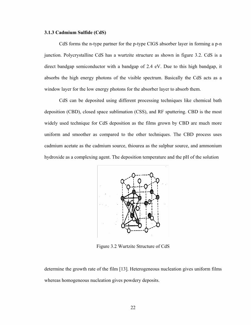
3.1.3 Cadmium Sulfide (CdS)
CdS forms the n-type partner for the p-type CIGS absorber layer in forming a p-n
junction. Polycrystalline CdS has a wurtzite structure as shown in figure 3.2. CdS is a
direct bandgap semiconductor with a bandgap of 2.4 eV. Due to this high bandgap, it
absorbs the high energy photons of the visible spectrum. Basically the CdS acts as a
window layer for the low energy photons for the absorber layer to absorb them.
CdS can be deposited using different processing techniques like chemical bath
deposition (CBD), closed space sublimation (CSS), and RF sputtering. CBD is the most
widely used technique for CdS deposition as the films grown by CBD are much more
uniform and smoother as compared to the other techniques. The CBD process uses
cadmium acetate as the cadmium source, thiourea as the sulphur source, and ammonium
hydroxide as a complexing agent. The deposition temperature and the pH of the solution
Figure 3.2 Wurtzite Structure of CdS
determine the growth rate of the film [13]. Heterogeneous nucleation gives uniform films
whereas homogeneous nucleation gives powdery deposits.

23
As some of the light is absorbed in the CdS, a current loss of approximately
6mA/cm2 is estimated [14]. Cd is a toxic material causing environmental concerns which
has led to the investigation of other materials to replace CdS as a window layer. The
other materials considered are ZnSe, ZnInxSey and InxSey [15]. Also ZnO has been tried
as a window layer [16].
3.1.4 Front Contact
The main requirements for a front contact are high conductivity and good
transparency. ZnO is the most widely used material for front contact in CIGS solar cells
as it has very high bandgap of 3.3 eV and has good optical and electrical properties. It is
typically n-type and can be deposited by different processing techniques like sputtering,
CVD, etc.
The bilayer ZnO is deposited using RF sputtering using a ceramic target. The first
layer is an intrinsic ZnO of about 500Å thickness deposited in Ar/O2 ambient. The
second layer is doped ZnO deposited in Ar ambient from a ZnO:Al2O3 target. The
amount of doping is a tradeoff between the electrical and optical properties. The
transmission drops off at higher wavelengths due to the free carrier absorption which is a
function of doping concentration. A transmission of 90% in the wavelength range of 400-
1000 nm with electrical resistivity of 9E-4 has been achieved [17]. Anti-reflecting
coating can be applied over the front contact to reduce reflection losses and aid in better
trapping of light.

24
3.2 Device Fabrication
The sequential steps followed in device fabrication are briefly discussed in this
section. A thin layer of Mo is deposited on a glass substrate using DC sputtering followed
by the CIGS absorber layer using a two stage process. A thin layer of CBD CdS is grown
over this absorber layer followed by a bilayer ZnO using RF sputtering.
3.2.1 Back Contact Deposition
The cleaning of the substrate is a very critical step in device fabrication to ensure
the removal of contaminants. Defects like scratches and contaminants find their way into
the device thereby hurting the device performance. The substrate is soaked in a detergent-
DI (deionized) water bath for about 3 hours and scrubbed to remove any particulates.
This is followed by several rinses in DI water followed by an ultrasonic treatment using
2Propanol. Several other solutions were tried but 2Propanol seems to give the best
results. Soaking of the glass substrates in a hot water bath for around 20 minutes follows
this ultrasonic treatment. The glass substrates are then stored in a DI water bath.
A 1 micron thick layer of Mo is deposited using DC magnetron sputtering. The
glass is heated to 150°C under vacuum before deposition to remove any moisture. The
glass substrate is heated in the load-lock and the deposition is done in the main deposition
chamber. The chamber is then pumped to a pressure of around 5 µtorr. The first layer of
3000Å is deposited at an argon pressure of 5 mT and the second layer of 7500Å at an
argon pressure of 1.5 mT. The resultant Mo film has a smooth surface and resistivities of
the order of 5E-5 ohm-cm.

25
3.2.2 Absorber Layer Deposition
Co-evaporation of metals from elemental sources is the most widely used
processing technique for high efficiency cells. NREL has developed a complex three
stage process for their high efficiency devices [18]. A high degree of control is required
in this process as it has a direct effect on the device performance. Hence a more suitable
process for commercial production is a two stage process.
This process involves the sequential deposition of the metal layers followed by
the high temperature anneal step in Se vapor. This process requires a small degree of
control because only one metal has to be controlled at a time and because of the self
controlling nature of Se flux at high temperatures. The two stage process consists of the
first stage of precursor formation followed by selenization at high temperature of about
550ºC. In the first stage, precursors are formed by sequential deposition of metals Cu, Ga,
In with or without Se. In the selenization step, these metals are reacted with Se at high
temperatures to form the CIGS compound. Any excess In and Ga if deposited is removed
from the surface during the selenization step which otherwise might precipitate around
the grain boundaries and hurt the device performance. The other technique to compensate
for the excess In and Ga is addition of extra Cu during the selenization step to form the
CIGS compound.
Shields were introduced between the metal sources to minimize the cross
contamination of sources during deposition. The precursor was formed using two
different configurations and they were named as Type I and Type V precursors. The
selenization step was also modified for some of the devices that were fabricated using the
Type V precursors.

26
3.2.2.1 Type I Precursors
The absorber layer was deposited in a new vacuum system which is a two
chamber load-locked system. In the type I precursor, Cu and Ga are deposited in the first
chamber and In and Se are deposited in the second chamber. The reason for building this
new system was to do the Cu and Ga depositions in a Se free atmosphere as compared to
the old system in which all the metal depositions were done in a Se background. The Se
flux during the absorber layer formation is high and once the system temperatures come
down the extra Se in the atmosphere sticks to the walls of the system. So during the
sequential deposition of the metals, this Se gets free and hence the metals are deposited in
Se background. In the new system the two chambers are isolated from each other using
an isolation valve and care is taken that none of the free Se enters the first chamber. The
metals are deposited at relatively low temperature of 275°C to complete the precursor
formation. A constant and high Se flux is maintained during the In2Se3 deposition. The
substrate temperature ensures that no excess Se sits on the surface. The source
arrangement and the thickness gradient for the metals are shown in figure 3.3.
Figure 3.3 Source Arrangement for Type I Precursor

27
A constant rate of 0.6 Å/sec is maintained during the copper deposition. The
thickness on the thickness monitor corresponds to around one-third that on the substrate.
A Constant rate of 0.7 Å/sec is maintained during Ga deposition and the thickness on the
substrate is one and half times that on the thickness monitor. During In2Se3 deposition the
In rate is maintained at 5.3 Å/sec and the Se flux is maintained at around 9.0 Å/sec. The
In thickness on the substrate is about half that on the thickness monitor, this is because
the source is placed at an angle to the substrate and so all the material that the crystal sees
does not reach the substrate. The Se flux varies from 19 Å/sec near the source to 16 Å/sec
away from the source. The Se flux is maintained at least three times that needed for
stoichiometric formation. This is necessary for good films [19].
Figure 3.4 Temperature Profile for Selenization for Type I Precursor
The precursor formation is followed by the selenization step in which the
substrate temperature is ramped upto 450°C in about 4 minutes which is then maintained

28
for about 7 minutes. The substrate temperature is again raised to 550°C in another 4
minutes remaining there for about 7 minutes. The substrate temperature is then turned off
but the substrate is exposed to Se flux till the substrate temperature comes down to about
400°C. The Se flux is maintained at about 9.0Å/sec during the whole of the selenization
process. A thin layer of copper is deposited to convert any excess In, Ga into CIGS
compound. The temperature profile is shown in figure 3.4.
3.2.2.2 Type V Precursor
Figure 3.5 Source Arrangement for Type V Precursor
In the type V precursor the Ga source is transferred from the first chamber to the
second chamber. With this new configuration co-evaporation of In, Ga and Se is possible.
This was also done to see whether the deposition of Ga in a Se background improves the
device performance. The source arrangement changes from the type I precursor and is
shown in figure 3.5 along with the thickness gradient. It was observed that the metal
ratios, which are maintained near unity, were more uniform over the sample. The Cu was
deposited as in the type I precursor. Some fraction of the total Ga was deposited first at

29
about 0.7Å/sec for better adhesion of the films. The remaining Ga was co-evaporated
with In and Se where a constant Ga rate of 0.3Å/sec was maintained. The actual thickness
on the substrate for Ga is again one and half times that on the thickness monitor The In
and Se rates were the same as in the type I precursor. Some experiments with the
substrate temperature were also carried out.
The selenization profile for the type V precursor was altered from the type I
precursor. The 450°C step in the original selenization was removed and the substrate
temperature was maintained at 550°C for about 16 minutes before turning the substrate
temperature off. The temperature profile for the altered selenization step is shown in
figure 3.6. Different temperature profiles were tried for the type V precursors and will be
discussed in the following chapter.
Figure 3.6 Temperature Profile for Selenization for Type V Precursor

30
3.2.3 Window Layer Deposition
A thin layer of CdS of about 300-500Å is grown on the absorber layer by
chemical bath deposition (CBD). The solution consists of a 0.015 molar cadmium acetate
solution, 0.15 molar solution of thiourea, 0.15 molar of ammonium hydroxide and DI
water. The substrate is immersed in the solution when the water bath temperature is
around 80°C with constant stirring of the solution. The deposition takes place for around
5-7 minutes approximately. If the substrate is kept immersed in the solution for a longer
time, then homogeneous nucleation of CdS is formed on the surface which is undesirable.
3.2.4 Front Contact Deposition
After the CdS deposition the substrate is blow dried using dry nitrogen gas. It is
then loaded in a vacuum chamber for the RF sputtering from the ZnO target. The
substrate is heated to around 125°C to remove any moisture absorbed during the CdS
deposition. The substrate is maintained at this temperature during the full front contact
deposition. A thin first layer of intrinsic ZnO is deposited in an Ar-O2 ambient followed
by the doped layer ZnO in Ar ambient. The substrate is masked using a stainless steel
mask, to form small dots of area 0.1 cm2, to understand the effect of thickness gradients
on the device performance.
3.3 Device Characterization
After the devices were fabricated, I-V measurements were done on them. The I-V
measurements were done using the Kiethley 2410 source meter. This source meter was
interfaced to the computer using a Labview program which also determines the Voc, the

31
FF and the Isc. The AM 1.5 global spectrum conditions are simulated using a lamp with
the intensity of one sun. A four-probe measurement is done on the 25 dots (masked
during the ZnO deposition). Before the measurements are done the absorber layer is
scrapped off to make contact with the Mo layer. Two probes are placed on the Mo back
contact and two probes are place on the ZnO front contact. The solar cell is biased over a
range of -0.2 to 0.5 V. Spectral response was done on these devices to know the current
density of the devices over the wavelength range of 400-1400 nm. The instrument used
for these measurements was an Oriel Spectrometer. This was also interfaced to the
computer using a Labview program. Silicon and germanium standards were used to
compare with the sample. The silicon standard was used over the wavelength range of
400-900 nm. The germanium standard was used over the wavelength range of 900-1400
nm. The quantum efficiency (QE) of the device was calculated and the QE vs.
wavelength graph was plotted.

32
CHAPTER 4
RESULTS AND DISCUSSIONS
The performance of CIGS solar cells, fabricated by the process discussed in the
earlier chapter is analyzed in this chapter. The main aim of this work is to optimize the
performance of these solar cells with regards to the parameters like Voc, Jsc and fill factor.
To do so a new process recipe will be developed to utilize the capabilities of the in-line
processing unit. The devices were analyzed using the I-V measurements and spectral
response. The main parameter used for analyzing the influence of process details on the
performance of the solar cell is the open circuit voltage. The short circuit current and the
fill factor are the additional parameters considered.
4.1 Effect of Bulk Copper
Because of new insights regarding fabrication in the in-line processing unit we
start by first re-optimizing the standard recipe. The bulk copper thickness was varied to
see its effect on device performance. Sample P044 had copper thickness of 594Å, P049
had 523 Å and P059 had 550 Å. Figure 4.1 shows the Voc distribution for the three
samples. Due the thickness gradient of all the metals the metal ratios are not same
throughout the sample. We can see that the Voc distribution is much more uniform in
sample P059 which can be attributed to the fact that the metal ratios are nearer to unity, in
the range of 1.0 to 0.94, throughout the sample. Some of the bad spots in these samples

33
could be due to the basic smudges and defects on the glass substrate. Table 4.1 shows the
effect of bulk copper thickness on the overall performance of the solar cells. As can be
seen from the table, the average Voc is better for sample P059 and so is the Isc. The fill
factors are also better for P059. The sample P044 has the worst device performance
because the metal ratios are greater than unity, in the range 1.1 to 1.03. As can be seen,
good Voc’s are attained in the lower left corner where the metal ratio is close to unity.
For sample P044 the metal ratios are in the range 0.97 to 0.91 and so the device
performance is not uniform.
Figure 4.1 Voc distributions for P044 (594 Å), P049 (523 Å) and P059 (550 Å)
Table 4.1 Effect of Cu Thickness on Device Performance
Sample Cu thickness
(Å)
Avg. Voc
(mV)
Avg. Isc
(mA)
Avg. F.F
(%)
P044 594 350 2.8 45
P049 523 390 2.9 48
P059 550 420 2.7 50

34
4.2 Effect of Venting on Jsc
Selenium is used in large quantities for each run so the source has to be filled for
every five runs. The system earlier had the problem that to open chamber 2, chamber 1
Figure 4.2 Spectral Response for Samples P007, P008, and H299
had to be vented first. It was observed that the Jsc of the device fabricated after the
system was vented was affected, and the Jsc improved with the run sequence. As can be
seen from table 4.2 the current density increases with the run sequence. It was speculated
that this could be due to Gallium oxidation or due to presence of water vapor. Figure 4.2
shows the spectral response for the two devices P007 and P008. The 3rd device is
fabricated by my colleague. The Voc’s are lower in these series or runs because the bulk
copper thickness was not optimized till then.
35
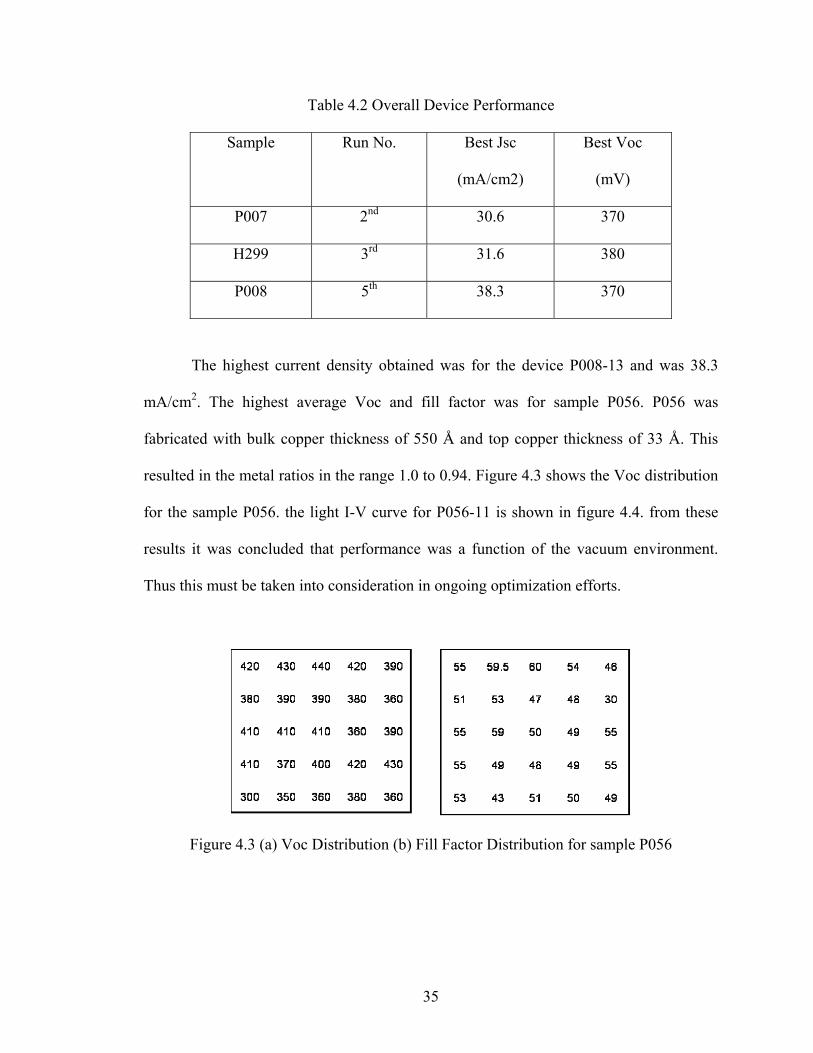
Table 4.2 Overall Device Performance
Sample Run No. Best Jsc
(mA/cm2)
Best Voc
(mV)
P007 2nd 30.6 370
H299 3rd 31.6 380
P008 5th 38.3 370
The highest current density obtained was for the device P008-13 and was 38.3
mA/cm2. The highest average Voc and fill factor was for sample P056. P056 was
fabricated with bulk copper thickness of 550 Å and top copper thickness of 33 Å. This
resulted in the metal ratios in the range 1.0 to 0.94. Figure 4.3 shows the Voc distribution
for the sample P056. the light I-V curve for P056-11 is shown in figure 4.4. from these
results it was concluded that performance was a function of the vacuum environment.
Thus this must be taken into consideration in ongoing optimization efforts.
Figure 4.3 (a) Voc Distribution (b) Fill Factor Distribution for sample P056

36
-0.02
0
0.02
0.04
0.06
0.08
0.1
0.12
-0.3 -0.2 -0.1 0 0.1 0.2 0.3 0.4 0.5
P056-11
Figure 4.4 I-V Characteristics of Device P056-11
4.2 Type V Precursors
In the type V precursor the Gallium is deposited in the second chamber. Here the
idea was to do co-evaporation of In, Ga and Se, but it was realized that the films were
having an adhesion problem if Ga was co-evaporated with In and Se. This could be
because, when co-evaporated enough Gallium does not segregate to the back of the
device, thus causing adhesion problems. Therefore around 25% of the total Ga to be
deposited was deposited by itself before the co-evaporation. Now the films were adhering
to the Mo back contact. In type V precursors copper was deposited first in chamber 1.
The substrate was then transferred to the 2nd chamber where about 25% of the total
Gallium was deposited first followed by the co-evaporation of In, Ga, and Se. The

37
bandgap shift for Type V device P066 when compared to a Type I device P056 is evident
in the figure 4.4. Since for our type I process we are not able to shift the bandgap unless
Cu is deposited in the 2nd chamber, this indicates a new controlling mechanism. This
could be cause because Gallium requires a CuxSey species to form CIGS.
Figure 4.5 Spectral Response for Samples P056 And P066
4.2.1 Effect of Ga Content on Device Performance
Sample P064 had about 12% and sample P066 has the Ga content of 20% of total
group III content. All other processing details were kept the same. We can see from
figure 4.5 that the overall Voc has improved for the sample P066. The device
performance of P064 is poor because when Gallium is co-evaporated with In and Se then
enough Gallium does not segregate to the back of the device. Thus when the Gallium
0
0.1
0.2
0.3
0.4
0.5
0.6
0.7
400 600 800 1000 1200 1400
P066 P056

38
content is increased to 20 % we see the improvement in the open circuit voltages as
Gallium can segregate to the back of the device with enough Gallium left to bond in the
space charge region. The other reason for the poor performance of P064 could be that it
was fabricated immediately after the system was vented. However, Voc would normally
not be affected this dramatically. It was seen that the short circuit current reduced as
compared to the type I devices; this could in part be attributed to the bandgap shift in the
type V devices. The bandgap shift results in fewer photons being absorbed and so fewer
electron-hole pairs generated. But the drop in Jsc is much greater than expected from the
bandgap shift, so other loss mechanisms are operative. This is not unlike the losses we
observe in Jsc when extra Ga is used in the type I process. In those case we attribute the
losses to improper bonded Ga, and that is likely the case here.
P064 P066
Figure 4.6 Voc Distribution for Ga Content

39
4.2.2 Effect of Substrate temperature
The substrate temperature during the precursor formation was changed from
275°C to 350°C for sample P071 keeping all other parameters the same. All the samples
had 20% Ga content of the total group III content. The Voc distribution for sample P071
is shown in figure 4.6. The Voc for this sample has gone down and it is speculated that it
could be due to the fact that the bonding of Gallium in the bulk of the film was not good
and there could be some Gallium present in the film in the form of GaxSey. The bandgap
shift for the samples P071 and P068 are comparable as can be seen from figure 4.7. So
we can say that enough Gallium is staying in the space charge region.
340 390 390 380 370
360 380 260 360 180
350 340 290 310 380
300 X 330 340 360
310 250 X 300 290
Figure 4.6 Voc distribution for sample P071

40
0
0.1
0.2
0.3
0.4
0.5
0.6
0.7
400 600 800 1000 1200 1400
P068 P071
Figure 4.8 Spectral Response of Samples P068 And P071
4.2.3 Effect of Selenization Profile on Device Performance
The selenization profile was changed for samples made under different
conditions. We will be considering two sets of samples here one with the substrate
temperature of 275°C and one with 350°C. The change in the selenization profile was
that the 450°C step was eliminated. Samples P067 and P072 had the new selenization
profile. Samples P071 and P072 have the substrate temperature of 350°C and samples
P067 and P069 have the substrate temperature of 275°C. The Voc distribution for
samples P071 and P072 is shown in the figure 4.8.
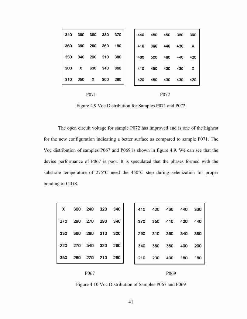
41
P071 P072
Figure 4.9 Voc Distribution for Samples P071 and P072
The open circuit voltage for sample P072 has improved and is one of the highest
for the new configuration indicating a better surface as compared to sample P071. The
Voc distribution of samples P067 and P069 is shown in figure 4.9. We can see that the
device performance of P067 is poor. It is speculated that the phases formed with the
substrate temperature of 275°C need the 450°C step during selenization for proper
bonding of CIGS.
P067 P069
Figure 4.10 Voc Distribution of Samples P067 and P069

42
4.3.3 Effect of Venting on Voc
It was observed that with the type V precursors the Voc is affected with the
chamber conditions. The Voc decreases when the second chamber is vented and it
increases with the run sequence. The table 4.3 shows the overall performance of the three
devices P065, P066 and P069. As the Gallium source is in the second chamber, it can
now be stated that the oxidation of Gallium source seems to be affecting the device
performance as it did for Ga deposited in chamber 1 for the type I process. Figure 4.11
shows the Voc distribution for the three devices. The same effect was observed when
copper was deposited in the second chamber for the type I device by my colleague. This
suggests that Gallium is not getting incorporated in the front of the device thus affecting
the bandgap shift as can be seen from figure 4.12 [19]. We can speculate the same reason
for the type V devices.
Table 4.3 Device Performance With Respect To Run Sequence
Sample Run No. Best Voc
(mV)
Avg. Voc
(mV)
Best F.F
(%)
Avg. F.F
(%)
P065 1st 410 350 49% 43%
P069 2nd 440 410 42% 38%
P066 3rd 480 440 51% 45%

43
P065 P069 P066
Figure 4.11 Voc Distribution of Samples P065, P066 and P069
Figure 4.12 Bandgap Shift with Run Sequence
The best device fabricated using the type V precursor is P072-08 with the highest open
circuit voltage of 500 mV, fill factor of 63% and Isc of 2.65 mA. The I-V curve for this

44
sample is shown in figure 4.13. The sample P072 was type V device with 20% Gallium
content and the substrate temperature was maintained at 350°C during precursor
formation. The selenization process was altered with the 450°C step being eliminated.
The current density for the type V precursor devices was low as compared to type I
devices. This again appears to be due tot eh negative effects of excess Ga that accompany
increased Ga incorporation and bonding. Thus co-evaporation of Ga with In and Se has
not solved this problem for this device process.
-0.003
-0.0025
-0.002
-0.0015
-0.001
-0.0005
0-0.3 -0.2 -0.1 0 0.1 0.2 0.3 0.4 0.5 0.6
P072-07
Figure 4.13 I-V Characteristics of Device P072-07

45
4.4 ZnSe Buffer Layer
Additional experiments were conducted with the window layer to determine their
role in device made with the processes discussed above. ZnSe was tried as a window
layer. ZnSe was evaporated on one half of sample P007 and CdS was deposited on the
other half. The substrate temperature during ZnSe deposition was maintained at around
200°C. About 300A of ZnSe buffer layer was deposited. Bilayer ZnO was then deposited
on both halves of the device. Voc’s were found to be comparable on both halves, but the
current density was very poor for the ZnSe half. Figure 4.14 shows the Voc distribution
for sample P007. This result suggests that Jsc’s are not just a function of bulk absorber
properties, but also of interface effects. Thus shortcomings in Jsc for the type V process
have to be further studied to determine where the Jsc losses are occurring so that the
process can be improved.
Figure 4.14 Voc Distribution for Sample P007
4.5 Effect of Silicon Nitride Layer
The influence of Sodium on the growth of CIGS films was observed some years
ago [20]. The Na from the soda lime glass substrate diffuses into the absorber and it

46
effects in better film morphology and higher conductivity of the film. But there is no
control over the amount of Na that diffuses.
Table 4.4 Overall Device Performance for Si3N4 Thickness Variation
Sample No. Si3 N4 Thickness Voc (mV) Isc (mA)
P015 200 Å 350 6.0
P016 800 Å 300 2.5
P017 1600 Å 290 0.3
Hence to better understand the role of Na in the CIGS films, a Si3N4 barrier layer was
deposited on the glass substrate before back contact deposition by a colleague who was
studying this effect [21]. Table 4.4 shows the overall device performance for type I
devices for different thickness of Si3N4 barrier layer. We can see from the table that as
the barrier layer thickness increases Voc and Jsc reduces. But Voc reduction is not as
dramatic as compared to the devices from the old system. This seems to be due to a
reduction in formation of CuxSey in the in-line chamber and is the subject of ongoing
studies.

47
CHAPTER 5
CONCLUSION AND RECOMMENDATIONS
In this study it is demonstrated that good device performance can be obtained for
the CIGS films fabricated by the two stage process. But there is still some scope for
improvement in the device performance. Type I devices with open circuit voltages of
around 450 mV and fill factors of around 60% were fabricated regularly. The highest
open circuit voltage obtained was 480 mV. The short-circuit currents of around 35
mA/cm2 with highest of 38mA/cm2 were fabricated.
It was seen that the bulk copper level mattered for the overall performance of the
sample. With bulk copper thickness of 550Å the metal ratios were nearer to unity, in the
range of 1.0 to 0.94, throughout the sample thus making the open circuit voltages uniform
even with the thickness gradient. This was seen even without adding the usual small
amount of top copper. If the copper thickness was increased to 594 Å then it adversely
affected the device performance, as the Cu/In ratio was greater than unity throughout the
sample. It was also observed that the chamber conditions affected the short circuit current
densities. The current densities increased as the chamber remained under vacuum for
longer time. This was due to a possible oxidation effect with Gallium or the presence of
water vapor in the chamber.

48
In the type I devices, Gallium has the tendency to segregate to the back, and so
there is little Gallium present in the space charge region. Hence there is no bandgap shift
relative to CIS. The open circuit voltage increases with increase in the bandgap as the
band bending increases. But the current density goes down with increasing bandgap. In
the voltage-current trade-off higher voltages and lower currents are preferred as the total
efficiency is not affected and the I2R losses are reduced. For this reason the type V
precursor was evaluated to see if the open circuit voltage could be increased by forcing
the incorporation of additional Gallium in the space charge region.
In the type V precursor it was seen that about 25% of the total Gallium to be
deposited had to be evaporated by itself first for better adhesion of the CIGS films to the
Mo back contact. Also it was seen that the Gallium content had to be increased as
compared to the type I devices for improving the device performance. The open circuit
voltages increased as compared to the type I device. This can be attributed to the fact that
enough Gallium was bonded in the space charge region to result in a bandgap shift.
Substrate temperature also proved to be an important parameter along with the
selenization profile for better device performance. It was observed that the substrate
temperature of 350°C and the selenization profile without the 450°C step gave the best
results for type V devices. It can be speculated that the 450°C step results in formation of
secondary phases which hurt device performance. Also if the substrate temperature is
kept at 275°C, then the 450°C step in the selenization profile is necessary as it probably
forms the required phases during the 450°C step. With the type V precursor the chamber
conditions seem to be affecting the device performance and the open circuit voltages in
particular. This could be due to the possible oxidation of the Gallium source when the

49
chamber is vented. It was observed that the Voc increased with every run from the time it
is vented.
Some of the experiments that need to be done to improve the device performance
are trying argon annealing of the samples with the type V precursors. Another thing that
needs to be tried is fabricating the type I precursor but with Gallium deposited in the
second chamber in selenium atmosphere as it is speculated that the Gallium will be
incorporated into the bulk of the film better improving the current density without
reducing the open circuit voltages too much. This is speculated because it has been
observed that when copper is deposited in selenium atmosphere the bandgaps open [20].

50
REFERENCE
[1] D.M.Chapin et al,”A New Silicon P-N Junction Photo-cell for Converting Solar Radiation into Electrical Power,” J.Appl. Phys., 25, 676, (1954)
[2] Y. Hamakawa et al,” Thin Film Solar Cells: Next Generation Photovoltaics and its Application,” Springer, Germany (2004)
[3] W.Horig et al,” The Optical Properties of CuInSe2 Thin Films,” Thin Solid Films, 48, 67, (1978)
[4] J.Kessler et al,” Electro-optical and Photoelectrochemical Studies of CuIn3Se5 Chalcopyrite Films,” Proceedings of the 23rd Photovoltacis Specialist Conference, 549, (IEEE, 1993)
[5] A.Rockett and R.W.Birkmire,” Current Status and Issues in Polycrystalline CuInSe2 for Photovoltaics application,” Proceedings of the MRS Meeting, V426, 143, (1996)
[6] L.L.Kazmerski, M.S.Ayyagi, Y.J.Juang, R.P.Patterson,” Growth and Characterization of Thin Film Compound Semiconductor Heterojunctions,” J.Vac.Sci.Tech., 13, 65, (1977)
[7] D.S.Albin et al,” A Study on the Optical and Microstructural Characteristics of Quaternary CIGS Polycrystalline Thin Films,” Proceedings of the 21st Photovoltacis Specialist Conference, 562, (IEEE, 1990)
[8] W.S.Chen et al,” Development of Thin Film Polycrystalline CuIn1-xGaxSe2 Solar Cells,” Proceedings of the 23rd Photovoltacis Specialist Conference, 577, (IEEE, 1993)
[9] W.N.Shafarman et al,” Characterization of CuInSe2 Solar Cells with High Ga Content,” Proceedings of the 25th Photovoltacis Specialist Conference, 898, (IEEE, 1995)
[10] M.A.Contreras et al, Progress in Photovoltaics, Res.Appl., 7, 311, (1999)
[11] S.M.Sze,” Physics of Semiconductor Devices,” Wiley, New York, (1981)
[12] J.H.Scofield et al,” Sputtered Mo Bilayer Contact for CuInSe2 Based Polycrystalline Thin Film Solar Cells,” Thin Solid Films, 260, 26, (1995)

51
[13] N.H.Schultz,” Solution Grown CdS Films for Photovoltaics,” M.S Thesis, University of South Florida, Tampa, (1991)
[14] R.H. Mauch et al,” Optimization of Windows in ZnO/CdS/CIS Heterojunctions,” Proceedings of the 22nd Photovoltacis Specialist Conference, 8989, (IEEE, 1991)
[15] Y.Ohtake et al,” CIGS Thin Film Solar Cells with Continuously Evaporated Cd-Free Buffer Layer,” Proceedings of the 25th Photovoltacis Specialist Conference, 549, (IEEE, 1995)
[16] R.Bhatt et al,” Dependance of Reactively Sputtered ZnO Electronic Properties on Growth Parameters for Use as a Buffer Layer in CIGS Solar Cells,” Proceedings of the 26th Photovoltacis Specialist Conference, 383, (IEEE, 1997)
[17] H.Sankaranarayanan, “ Effective Processing Conditions for CIGS Solar Cells Using an Additional Cu Layer,” M.S. Thesis, University of South Florida, Tampa, (1998)
[18] M.A.Contreras et al,” High Efficiency CIGS Based Thin Film Solar Cells: Processing of Novel Absorber Layer,” Proceedings of the 24th Photovoltacis Specialist Conference, 68, (IEEE, 1994)
[19] S.A. Zafar,”Growth and Characterization of Thin Film ZnO and CIGS For Photovoltaic Applications,” PhD Dissertation, University of South Florida, Tampa, (1997)
[20] H.Sankaranarayanan, “Processing of CIGS Solar Cells using a Two-Step Process,” PhD Dissertation, University of South Florida, Tampa, (2004)
[21] V. Mohankrishanaswamy,” Processing and Characterization of CIGS Solar Cells”, M.S. Thesis, University of South Florida, Tampa, (2004)