optical characterization by spectroscopic...
TRANSCRIPT

Optical Characterization By Spectroscopic Ellipsometry.
Ron SynowickiJ.A. Woollam Co., Inc.
Georgia Tech., December 2010

© 2010, All Rights Reserved 2
Morning Overview
Spectroscopic Ellipsometry:– Part 1: Basic Theory of Ellipsometry.– Part 2: Standard Applications.
Break– Part 3: Grading and Anisotropy.– Part 4: Infrared and In-Situ Ellipsometry.

© 2010, All Rights Reserved
Light & Wavelength Units1. Wavelength (Å, nm, or microns)
2. Photon Energy (eV).
3. Wavenumber (cm-1). Used Mid to Far IR.
,12400
ÅeVE λ= ,1240
nmeVE λ=
meVE
μλ240.1
=
m
cmμλ
100001 =−
Y
X
Z
Electric field, E(z,t)
λ
© 2010, All Rights Reserved
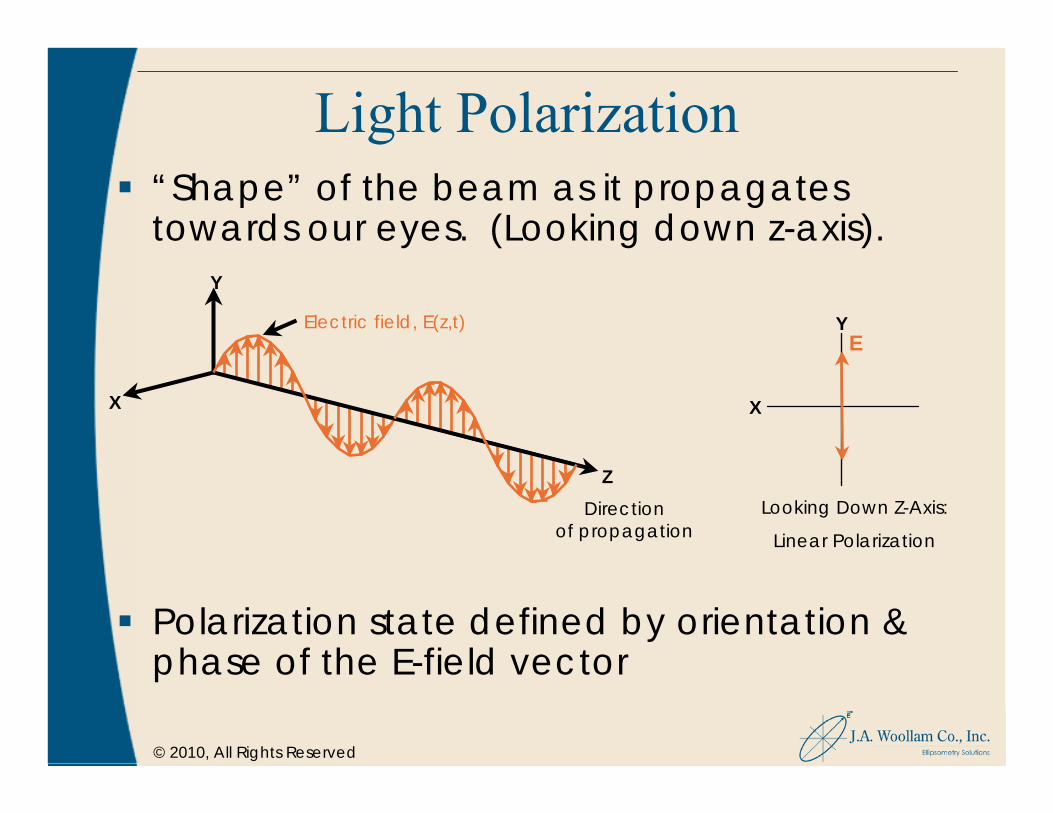
Light Polarization“Shape” of the beam as it propagates towards our eyes. (Looking down z-axis).
Polarization state defined by orientation & phase of the E-field vector
Y
X
Z
Electric field, E(z,t)
Directionof propagation
X
Y
Looking Down Z-Axis:
Linear Polarization
E

5© 2010, All Rights Reserved
Linearly Polarized LightOrthogonal EX & EY propagating in same
direction. Component waves are in phase with each other.Result : linearly polarized wave.– the 'plane of vibration' depends on relative
amplitudes of Ex & EY
Y
wave1
wave2X
E

6© 2010, All Rights Reserved
Circularly Polarized Light
Orthogonal EX & EY: 90° out-of-phase & equal in amplitude with each otherResult : circularly polarized wave
Y
X
Z
wave1
wave2 E
E (t)y
tX
Y
Net E-fieldE (t)x
tLooking Down Z-Axis
7© 2010, All Rights Reserved
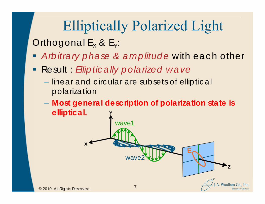
Elliptically Polarized Light
Y
X
Z
wave1
wave2E
Orthogonal EX & EY: Arbitrary phase & amplitude with each otherResult : Elliptically polarized wave– linear and circular are subsets of elliptical
polarization– Most general description of polarization state is
elliptical.
© 2010, All Rights Reserved
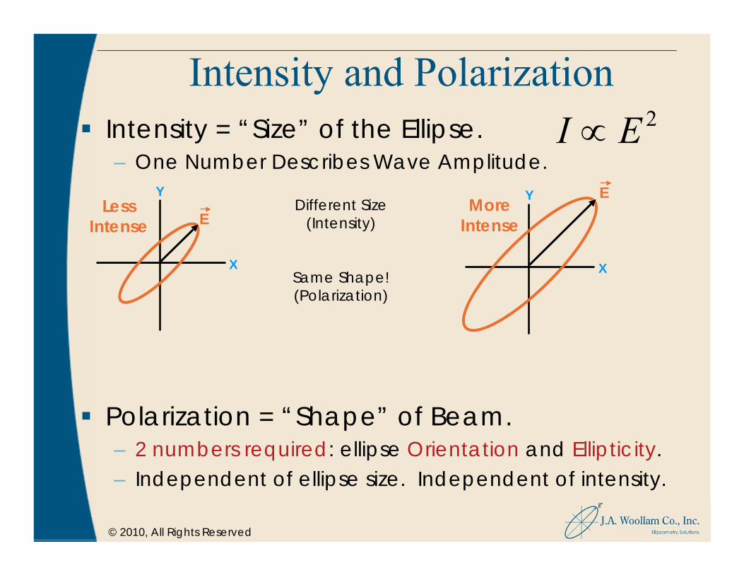
Intensity and PolarizationIntensity = “Size” of the Ellipse. – One Number Describes Wave Amplitude.
Polarization = “Shape” of Beam.– 2 numbers required: ellipse Orientation and Ellipticity.– Independent of ellipse size. Independent of intensity.
X
Y
ELess
Intense
X
Y EMore
Intense
2EI ∝
Different Size (Intensity)
Same Shape! (Polarization)

9© 2010, All Rights Reserved
Ellipsometry Overview
Measure the change in polarization of light reflected from surface.
Horizontal (s-) and Vertical (p-) components present.
plane of incidence
E
E
p-plane
p-plane
s-plane
s-plane
1. linearly polarized light ...
2. reflect off sample ...
3. elliptically polarized light !
s
pi
RR
eρ ~~
)ψtan( == Δ

© 2010, All Rights Reserved
EllipsometersEvery Ellipsometer contains the same basic components
SE also needs wavelength selection.
PolarizationGenerator Polarization
Analyzer
Sample
LightSource Detector

© 2010, All Rights Reserved
Hardware: Optical Components
Optical components needed for any ellipsometer:
Light Source(s)Two Polarizers (Polarizer & Analyzer)Compensator (Optional, but desirable)Detector(s)

© 2010, All Rights Reserved
Ellipsometer Types
Null Ellipsometer
Light
Sou
rce D
etector
P
P
P
P
P
A
A
A
A
A
S
S
S
S
S
C
M
C
Rotating Analyzer (RAE)
Rotating Polarizer (RPE)
Rotating Compensator (RCE)
Polarization Modulation (PME)

13© 2010, All Rights Reserved
Ellipsometry AdvantagesMeasures ratio of two values!!!– highly accurate & reproducible (even at low light
levels).– no reference necessary.
Measures a 'phase‘ quantity, ‘Δ’– very sensitive, especially to ultrathin films (<10 nm).
Spectroscopic Ellipsometry (SE)– increased sensitivity to multiple layer film stacks.– eliminates ‘period’ problem for thick films. Problem
with single-λ.– measures data at wavelengths of interest…193,
633 nm, 1550 nm, bandgaps, etc.Variable Angle Spectroscopic Angle (VASE)– new information (different path length) with each
angle optimizes sensitivity.

© 2010, All Rights Reserved
SE Experiment SummaryCONCLUSIONS:
– Light is reflected or transmitted from a sample.
– The polarization state of incoming light is known.
– The polarization state of reflected/transmitted light is measured.
– An accurate ellipsometer can determine Ψand Δ from the sample.

15© 2010, All Rights Reserved
Optical Properties: Basic TheoryInteraction of Light With Materials:
Goal: Provide a basic background on:Propagation of light in materials. Optical constants:– Dielectrics– Metals– Semiconductors
Optical Absorption.– Mechanical Analogies.– Absorption Coefficient
Brewster’s Angle.– Optimum Angles for ellipsometry.
Coated Samples with many reflections. – Fresnel Coefficients. Interference effects.

© 2010, All Rights Reserved
Polarization ChangesReflections occur from:– Uncoated “Bulk” Substrates.– Thin film Samples (Coatings).
Reflections caused by:– DIFFERENCES in Refractive Index at
interfaces…– Air to glass, Glass to Silicon, etc.
Need to further understand Refractive index.
Rn n
n n=
−
+
( )
( )0 1
2
0 12
For Uncoated SubstrateAt Normal Incidence.

© 2010, All Rights Reserved
Refractive Index: What is it?Refractive Index = Optical “Density”– Impediment to propagation of light.– Speed in vacuum: c = 3x10⁸ m/s.– Wave speed in material = c/n
– Analogy:– Walking along the beach (easy).– Wading through water (harder).
– n(air) = 1.00; Reference Value.– n(glass)= 1.50– n(water) = 1.33

© 2010, All Rights Reserved
LightVelocity and wavelength vary in different materials.
Energy of photon:
Frequency, ν of wave remains constant!(Conservation of Energy.)
nc
=v
λυ v=
n = 1 n = 2
)(240,1)(nm
heVEλ
υ ≅=
speed of lightspeed of light
Planck’s constantPlanck’s constant

© 2010, All Rights Reserved
Refractive IndexDetermines Wave speed.
ν = c/n
Determines Angle of Propagation.– Snell’s Law of Refraction:
n1sinθ1 = n2sinθ2
– Pencil in glass of water appears “Broken”.

© 2010, All Rights Reserved
Absorption and ExtinctionAbsorption With Depth
For Absorbing Bulk Materials:= deeper propagation. = more energy loss.= complete extinction.
As absorbing films become thicker:= longer propagation path in film.= wave spends longer time in film.= more absorption by material.= more extinction of wave.
λπα k4
=zoeIzI α−=)(
z

© 2010, All Rights Reserved
Absorption CoefficientAbsorption with Depth:
– Exponential Absorption with depth, z, or film thickness.
I(z) =Imaxe-αz
– Exponential Decay of wave.
Absorption Coefficient, α:α(λ) = 4πk(λ)/λ
– Units: 1/(length) (1/nm, 1/microns, 1/Å, etc.)

© 2010, All Rights Reserved
Complex Refractive Index.Both n and k are needed to describe real materials.n = “Refractive Index”– Gives wave speed = c/n.– Gives direction of propagation = refraction angle.
• Snell’s Law
k = “Extinction Coefficient”– Loss of energy in wave. Intensity is “Extinguished.”
Both n and k vary with wavelength.– Index Dispersion: One reason for doing Spectroscopic
ellipsometry.Together called “Complex Refractive Index”:
ñ(λ) = n(λ) + ik(λ)
© 2010, All Rights Reserved
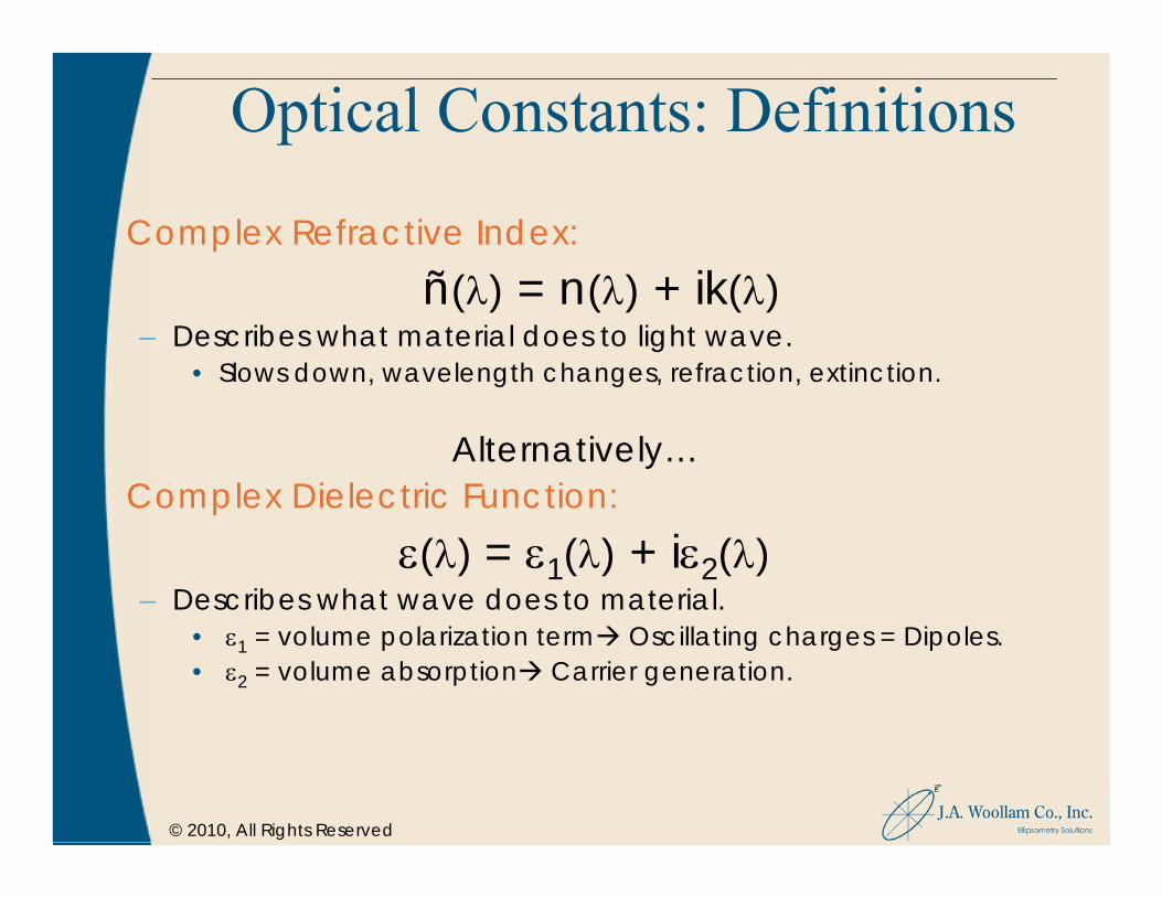
Optical Constants: Definitions
Complex Refractive Index:ñ(λ) = n(λ) + ik(λ)
– Describes what material does to light wave.• Slows down, wavelength changes, refraction, extinction.
Alternatively…Complex Dielectric Function:
ε(λ) = ε1(λ) + iε2(λ)– Describes what wave does to material.
• ε1 = volume polarization term Oscillating charges = Dipoles.• ε2 = volume absorption Carrier generation.
© 2010, All Rights Reserved
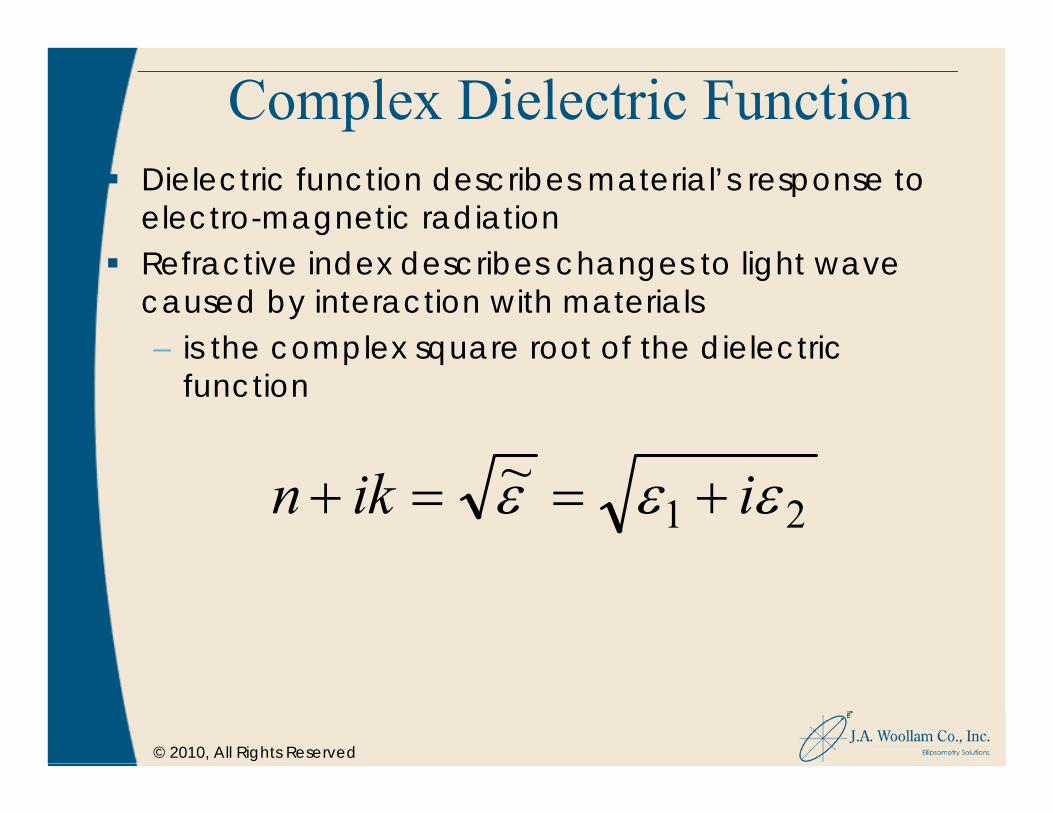
Complex Dielectric FunctionDielectric function describes material’s response to electro-magnetic radiationRefractive index describes changes to light wave caused by interaction with materials – is the complex square root of the dielectric
function
21~ εεε iikn +==+

© 2010, All Rights Reserved
Optical Constants: ConversionsConverting dielectric function & refractive index.
At each wavelength:
WVASE32 will do these conversions automatically!
221 )( ikni +=+= εεε
nk22 =ε221 kn −=ε
n =+ +[ ( ) ]ε ε ε1 1
222
2k =
− + +[ ( ) ]ε ε ε1 12
22
2

© 2010, All Rights Reserved
Optical AbsorptionAbsorption can also occur: (k > 0). Four causes of Absorption:– 1. Free electrons absorb wave energy.
• Metals, Semiconductors Conductivity.– 2. Electrons bound to atoms in material.
• Dielectrics. Oscillating electron clouds. Heat Losses.– 3. Electrons broken free from bound states.
• Bound electrons become free electrons.• Occur at higher energies in visible and UV.
– 4. Vibrations of atoms or molecules.• Infrared spectroscopy. λ=2 microns and longer.
Consider each type separately.

© 2010, All Rights Reserved
Optical ConstantsDifferent regions represent different absorptions.
ε
Photon Energy (eV)0.03 0.1 0.3 1 3 10
ε 1 2
-50
-38
-25
-13
0
13
25
0
10
20
30
40
50
60
ε1ε2
LatticeVibrations
ElectronicTransitions
UVIR Visible
Rutile TiO2, UV to IR Spectral Range
Transparent

© 2010, All Rights Reserved
Metals: Refractive IndexMetals: Have more electrons than needed for bonding. (Covalent Bonds = Sharing of electrons).“Extra” electrons not shared are set “free” by the atoms. Travel freely in the material. Absorb Light.
Free electrons give:– Electrical Conduction.– Optical absorption.
Applied field of light wave causes electrons to move! Wave energy lost as heat.

© 2010, All Rights Reserved
Dielectrics: Refractive IndexOscillating electron charge cloud.
Electrons can move easily. Very light.Heavy atomic cores move hardly at all.Displaced charge = Electric Dipoles.
Photon In

© 2010, All Rights Reserved
Dielectrics: Refractive IndexOSCILLATIONS TAKE TIME!– Wave must start charge cloud moving. “Push” electrons out
of way.– Moving charge cloud will re-emit wave. No energy lost!!– Re-emitted wave is “Delayed” in phase.
WAVE HAS BEEN SLOWED!!Refractive Index, n = (speed in air)/(speed in material)
Analogy: Walking in water.– You must push water out of the way.– You become slowed down.
Reference Wave
In Phase Out of Phase
© 2010, All Rights Reserved
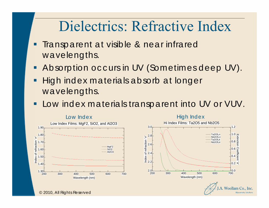
Dielectrics: Refractive IndexTransparent at visible & near infrared wavelengths.Absorption occurs in UV (Sometimes deep UV).High index materials absorb at longer wavelengths.Low index materials transparent into UV or VUV.
Hi Index Films: Ta2O5 and Nb2O5
Wavelength (nm)200 300 400 500 600 700
Inde
x of
refra
ctio
n 'n
'
Extinction C
oefficient 'k'
2.0
2.2
2.4
2.6
2.8
3.0
0.0
0.2
0.4
0.6
0.8
1.0
1.2
Ta2O5, nNb2O5, nTa2O5, kNb2O5, k
Low Index Films: MgF2, SiO2, and Al2O3
Wavelength (nm)200 300 400 500 600 700
Inde
x of
refra
ctio
n 'n
'
1.30
1.40
1.50
1.60
1.70
1.80
1.90
MgF2SiO2Al2O3
Low Index High Index
© 2010, All Rights Reserved
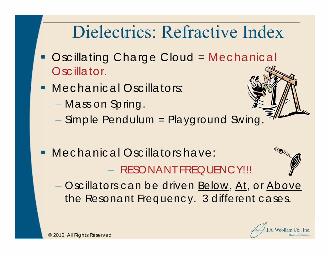
Dielectrics: Refractive IndexOscillating Charge Cloud = Mechanical Oscillator.Mechanical Oscillators:– Mass on Spring.– Simple Pendulum = Playground Swing.
Mechanical Oscillators have:– RESONANT FREQUENCY!!!
– Oscillators can be driven Below, At, or Abovethe Resonant Frequency. 3 different cases.
© 2010, All Rights Reserved
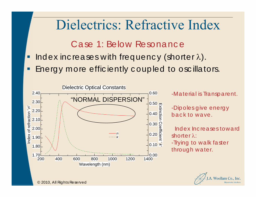
Dielectrics: Refractive IndexCase 1: Below Resonance
Index increases with frequency (shorter λ).Energy more efficiently coupled to oscillators.
Dielectric Optical Constants
Wavelength (nm)200 400 600 800 1000 1200 1400
Inde
x of
refra
ctio
n 'n
'
Extinction C
oefficient 'k'
1.70
1.80
1.90
2.00
2.10
2.20
2.30
2.40
0.00
0.10
0.20
0.30
0.40
0.50
0.60
nk
-Material is Transparent.
-Dipoles give energy back to wave.
Index Increases toward shorter λ:-Trying to walk faster through water.
“NORMAL DISPERSION”

© 2010, All Rights Reserved
Dielectrics: Refractive IndexCase 2: Resonance
Maximum amplitude of Electron clouds.Neighboring clouds begin to interact with each other.
Dielectric Optical Constants: At Resonance
Wavelength (nm)200 300 400 500 600
Inde
x of
refra
ctio
n 'n
'
Extinction C
oefficient 'k'
1.70
1.80
1.90
2.00
2.10
2.20
2.30
2.40
0.00
0.10
0.20
0.30
0.40
0.50
0.60
nk
Absorption due toe-cloud “bumping”.
Energy taken fromDipoles, given to k.
Electron Clouds Bump.Lose energy as heat.

© 2010, All Rights Reserved
Index DispersionOptical constants vary with wavelength:
ñ(λ) = n(λ) + ik(λ)
Real and imaginary optical properties are not independent (Kramers-Kronig consistent).
Normal Dispersion:(transparent wavelengths)
No absorption present (k=0),Index decreases as wvl increases
Normal Dispersion:(transparent wavelengths)
No absorption present (k=0),Index decreases as wvl increases
Anomalous Dispersion:(absorbing wavelengths)
Absorption in material causeswvl-dependent changes in indexas described by K-K consistency
Anomalous Dispersion:(absorbing wavelengths)
Absorption in material causeswvl-dependent changes in indexas described by K-K consistency

© 2010, All Rights Reserved
Dielectrics: Refractive IndexMultiple resonant absorptions often occur.Organic AR Coating.
AZ BARLi ARC Optical Constants
Wavelength in nm0 200 400 600 800 1000 1200
Inde
x of
refra
ctio
n 'n
'
Extinction C
oefficient 'k'
1.2
1.4
1.6
1.8
2.0
2.2
0.0
0.2
0.4
0.6
0.8
1.0
nk
© 2010, All Rights Reserved
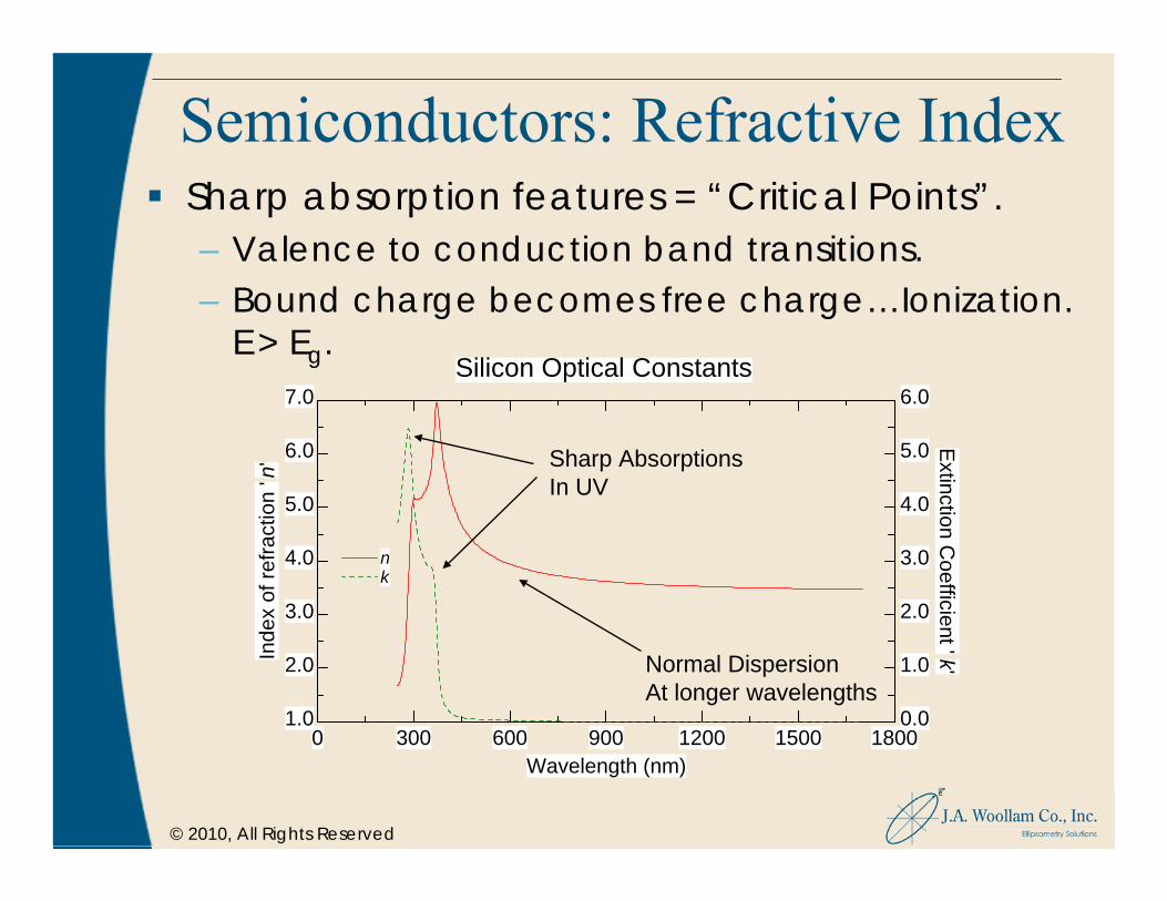
Semiconductors: Refractive IndexSharp absorption features = “Critical Points”.– Valence to conduction band transitions.– Bound charge becomes free charge…Ionization.
E > Eg.Silicon Optical Constants
Wavelength (nm)0 300 600 900 1200 1500 1800
Inde
x of
refra
ctio
n 'n
'
Extinction C
oefficient 'k'
1.0
2.0
3.0
4.0
5.0
6.0
7.0
0.0
1.0
2.0
3.0
4.0
5.0
6.0
nk
Sharp AbsorptionsIn UV
Normal DispersionAt longer wavelengths
© 2010, All Rights Reserved
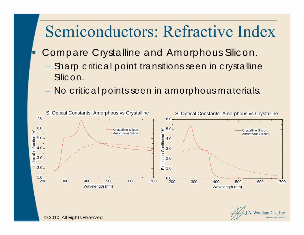
Semiconductors: Refractive IndexCompare Crystalline and Amorphous Silicon.– Sharp critical point transitions seen in crystalline
Silicon.– No critical points seen in amorphous materials.
Si Optical Constants: Amorphous vs Crystalline
Wavelength (nm)200 300 400 500 600 700
Inde
x of
refra
ctio
n 'n
'
1.0
2.0
3.0
4.0
5.0
6.0
7.0
Crystalline SiliconAmorphous Silicon
Si Optical Constants: Amorphous vs Crystalline
Wavelength (nm)200 300 400 500 600 700
Ext
inct
ion
Coe
ffici
ent '
k'
0.0
1.0
2.0
3.0
4.0
5.0
6.0
Crystalline SiliconAmorphous Silicon

© 2010, All Rights Reserved
Semiconductors: Refractive IndexPolycrystalline Silicon: Optical constants change with
crystallinity.
© 2010, All Rights Reserved
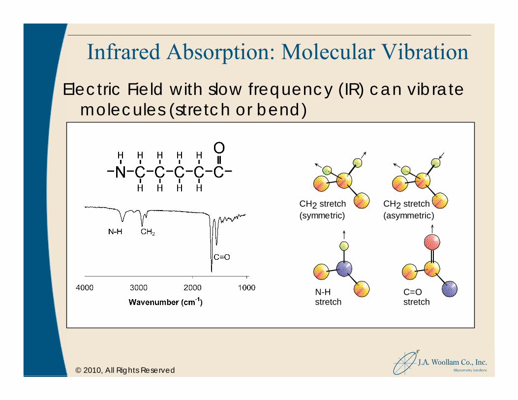
Infrared Absorption: Molecular VibrationElectric Field with slow frequency (IR) can vibrate
molecules (stretch or bend)
CH2 stretch(symmetric)
CH2 stretch(asymmetric)
N-Hstretch
C=Ostretch
© 2010, All Rights Reserved
Optical AbsorptionReview:
4 major types studied.Metals.– Free Carrier Absorption.
Dielectrics.– Resonant Absorption.
Semiconductors.– Resonant absorption below band gap.– Bound to free electron transitions at band gap Eg and
above.– Free carriers above band gap…Interband transitions.
Infrared Wavelengths.– Vibrational absorption of molecules.

© 2010, All Rights Reserved
Dispersion EquationsMathematical representations of optical constantsas a function of wavelengthAdvantages:– Easily adjust optical constants with only a few
“free” parameters.– No noise– Easier to interpolate or extrapolate– Often maintain K-K consistency
Transparent Types:– Cauchy and Sellmeier

© 2010, All Rights Reserved
Normal Dispersion: Cauchy ModelUsed to describe index of refraction (n) of transparent materials (k=0). Three parameters (A, B, C) describe index versus wavelength (λ).
n(λ)=A+B/λ2+C/λ4
k(λ)=0
Wavelength (nm)200 400 600 800 1000 1200
Inde
x of
refra
ctio
n 'n
'
1.44
1.47
1.50
1.53
1.56
1.59
1.62
1.65A sets index range
B and C give dispersion shape

© 2010, All Rights Reserved
Anomalous Dispersion: Oscillator ModelsAll Oscillator models have 3 parameters in common:
• 1. Amplitude (Amp) or “Strength”• 2. Broadening (Br)…”Width”• 3. Center energy (Ec) or wavelength…”position”
Wavelength (nm)0 300 600 900 1200 1500 1800
Rea
l(Die
lect
ric C
onst
ant),
ε 1Im
ag(Dielectric C
onstant), ε2
0.4
0.6
0.8
1.0
1.2
1.4
1.6
0.0
0.2
0.4
0.6
0.8
1.0
1.2
ε1ε2
Amp
Ec
Br
© 2010, All Rights Reserved
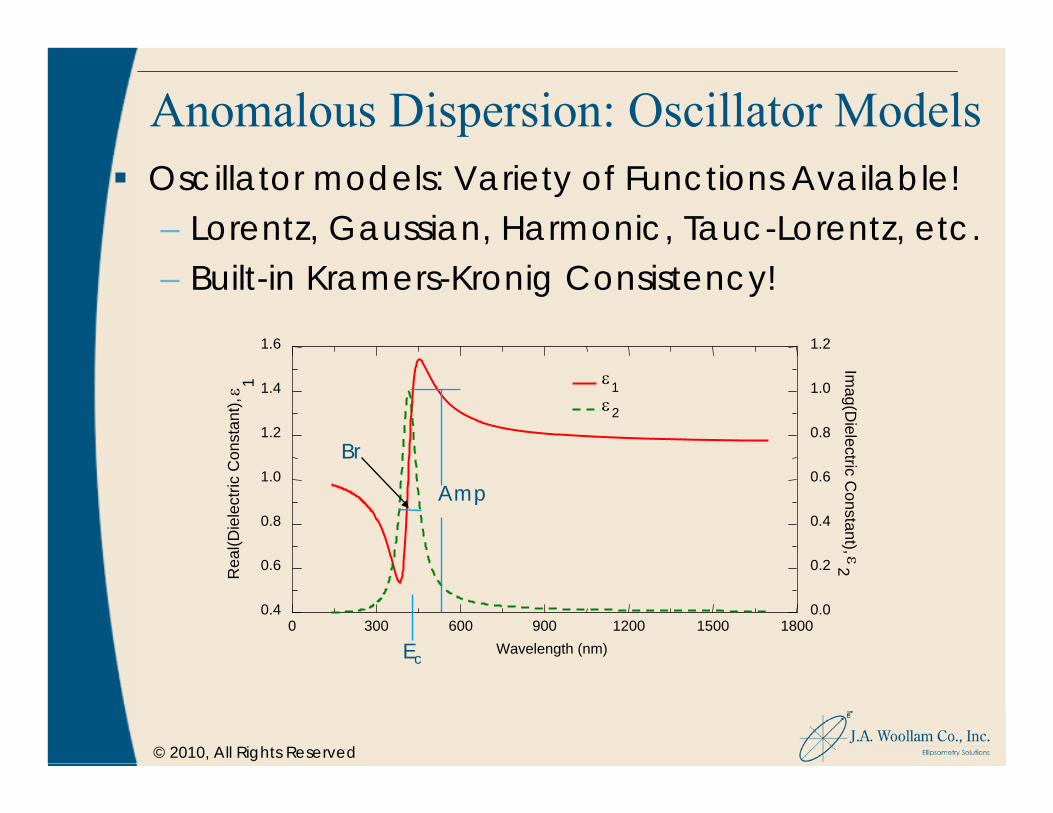
Anomalous Dispersion: Oscillator ModelsOscillator models: Variety of Functions Available!– Lorentz, Gaussian, Harmonic, Tauc-Lorentz, etc.– Built-in Kramers-Kronig Consistency!
Wavelength (nm)0 300 600 900 1200 1500 1800
Rea
l(Die
lect
ric C
onst
ant),
ε 1
Imag(D
ielectric Constant), ε
2
0.4
0.6
0.8
1.0
1.2
1.4
1.6
0.0
0.2
0.4
0.6
0.8
1.0
1.2
ε1ε2
Amp
Ec
Br

© 2010, All Rights Reserved
Multiple Absorptions: Ensemble ModelDielectric function can be modeled as an sum or ensemble of various oscillators
– Different Oscillator can be used for each absorption region– Oscillators are summed together.
– Remains KK-consistent.
( ) ∑+=n
nntypeoffset AmpOsc ,...),,(~ γωεωε
Photon Energy (eV)0.0 1.0 2.0 3.0 4.0 5.0
Imag
(Die
lect
ric C
onst
ant),
ε 2
0.0
0.5
1.0
1.5
2.0
2.5
ito pbpdrudegaussiantauc-lorentz
Drude
Gaussian
Tauc-Lorentz
© 2010, All Rights Reserved
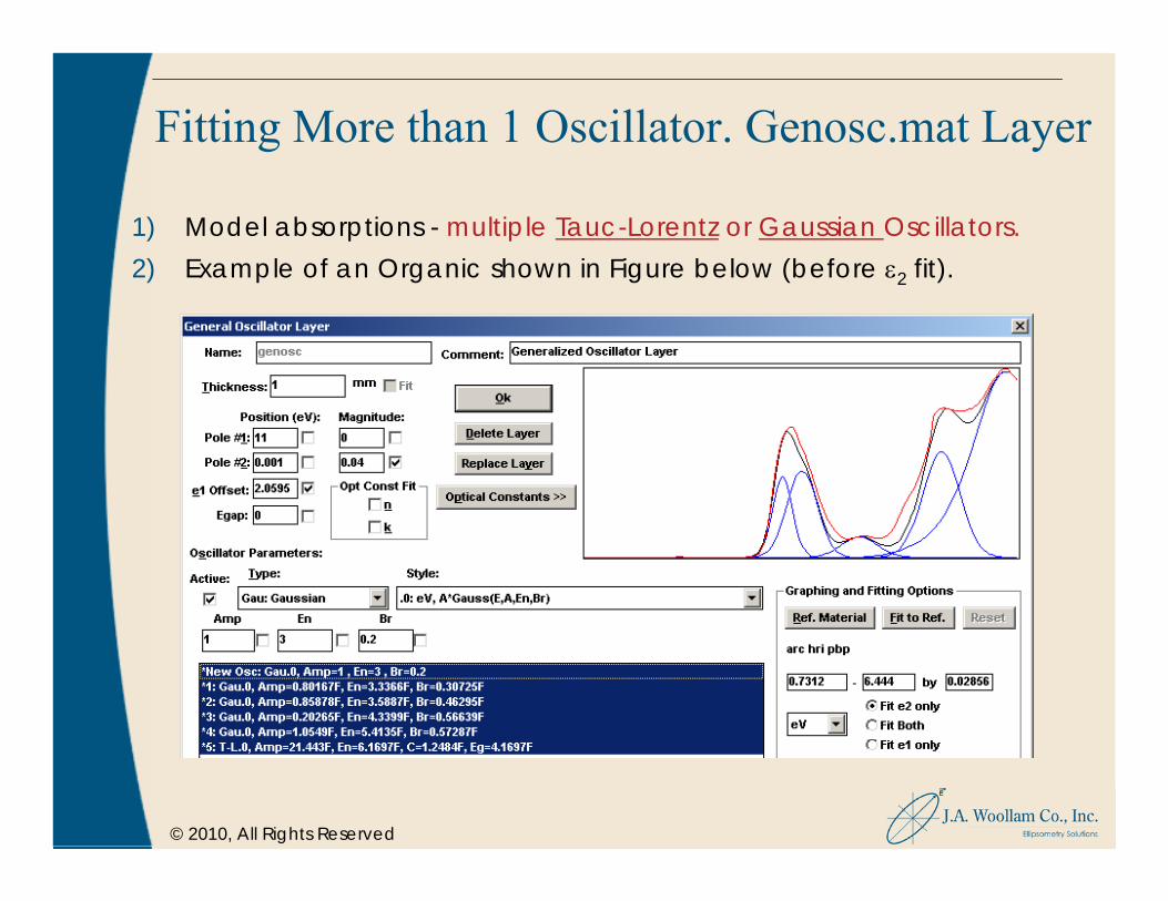
Fitting More than 1 Oscillator. Genosc.mat Layer
1) Model absorptions - multiple Tauc-Lorentz or Gaussian Oscillators.2) Example of an Organic shown in Figure below (before ε2 fit).

© 2010, All Rights Reserved
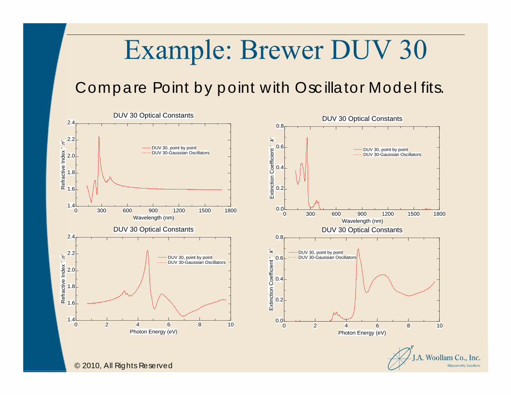
Example: Brewer DUV 30 PolymerUse 14 Gaussian oscillators to fit point by point results.Data fit 130-1700 nm.
© 2010, All Rights Reserved
Example: Brewer DUV 30
DUV 30 Optical Constants
Photon Energy (eV)0 2 4 6 8 10
Ext
inct
ion
Coe
ffici
ent '
k'
0.0
0.2
0.4
0.6
0.8
DUV 30, point by pointDUV 30-Gaussian Oscillators
DUV 30 Optical Constants
Wavelength (nm)0 300 600 900 1200 1500 1800
Ext
inct
ion
Coe
ffici
ent '
k'
0.0
0.2
0.4
0.6
0.8
DUV 30, point by pointDUV 30-Gaussian Oscillators
DUV 30 Optical Constants
Wavelength (nm)0 300 600 900 1200 1500 1800
Ref
ract
ive
Inde
x '
n'
1.4
1.6
1.8
2.0
2.2
2.4
DUV 30, point by pointDUV 30-Gaussian Oscillators
DUV 30 Optical Constants
Photon Energy (eV)0 2 4 6 8 10
Ref
ract
ive
Inde
x '
n'
1.4
1.6
1.8
2.0
2.2
2.4
DUV 30, point by pointDUV 30-Gaussian Oscillators
Compare Point by point with Oscillator Model fits.
© 2010, All Rights Reserved
Example: Brewer DUV 30
0 si_vuv 1 mm1 duv30-14 oscillators 609.64 Å
Generated and Experimental
Photon Energy (eV)0 2 4 6 8 10
Ψ in
deg
rees
0
20
40
60
80
100
Model Fit Exp E 65°Exp E 70°Exp E 75°
Generated and Experimental
Photon Energy (eV)0 2 4 6 8 10
Δ in
deg
rees
-100
0
100
200
300
Model Fit Exp E 65°Exp E 70°Exp E 75°
Data Fit 130-1700 nm.
Oscillator Model Fit.
© 2010, All Rights Reserved
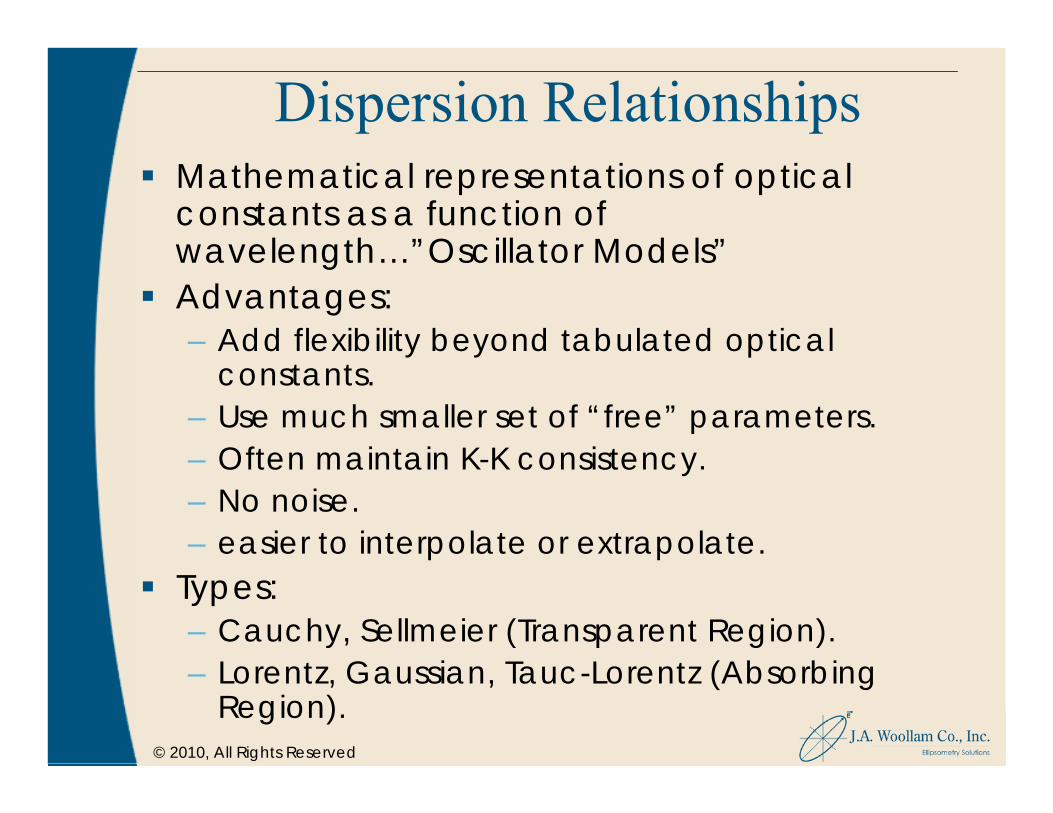
Dispersion RelationshipsMathematical representations of optical constants as a function of wavelength…”Oscillator Models”Advantages:– Add flexibility beyond tabulated optical
constants.– Use much smaller set of “free” parameters.– Often maintain K-K consistency.– No noise.– easier to interpolate or extrapolate.
Types:– Cauchy, Sellmeier (Transparent Region).– Lorentz, Gaussian, Tauc-Lorentz (Absorbing
Region).

© 2010, All Rights Reserved 52
Thin Film InterferenceEach reflected wave has phase and amplitude.
0~n
1~n
2~n

© 2010, All Rights Reserved 53
Thick versus ThinThicker films have more interference oscillationsOscillations provide information about Δnand thickness
•500nm
•Wavelength (nm)•0 •300 •600 •900 •1200 •1500 •1800
•Ψ•in
deg
rees
•0
•20
•40
•60
•80
•100
•Exp E 75°
•5 micron Oxide
•Wavelength (nm)•0 •300 •600 •900 •1200 •1500 •1800
•Ψ•in
deg
rees
•0
•20
•40
•60
•80
•100
•Exp E 75°
•100nm Oxide
•Wavelength (nm)•0 •300 •600 •900 •1200 •1500 •1800
•Ψ•in
deg
rees
•0
•20
•40
•60
•80
•100
•Exp E 75°

© 2010, All Rights Reserved
Data Acquisition
Wavelengths (Range and Number)?– Wavelengths of interest? – Where is film transparent?– Film Thickness?– Sharp features in data?
Angles?– What are Substrate and Films? – Single or Multilayers?– Complex materials?

© 2010, All Rights Reserved
Wavelengths?Resolve data features.
Experimental Data
Wavelength (nm)0 300 600 900 1200 1500 1800
Ψ in
deg
rees
0
20
40
60
80
100Exp E 65°Exp E 75°Data every 2nm
2.5 μm Oxide
20 nm0.1 eV< 200 nm
2 nm,Long wavelengths
>3 μm
2 nm0.01eV1 -3 μm
5 nm0.025 eV500 nm - 1 μm
10 nm0.05 eV200 - 500 nm
Steps (nm)Steps (eV)
Film Thickness
© 2010, All Rights Reserved
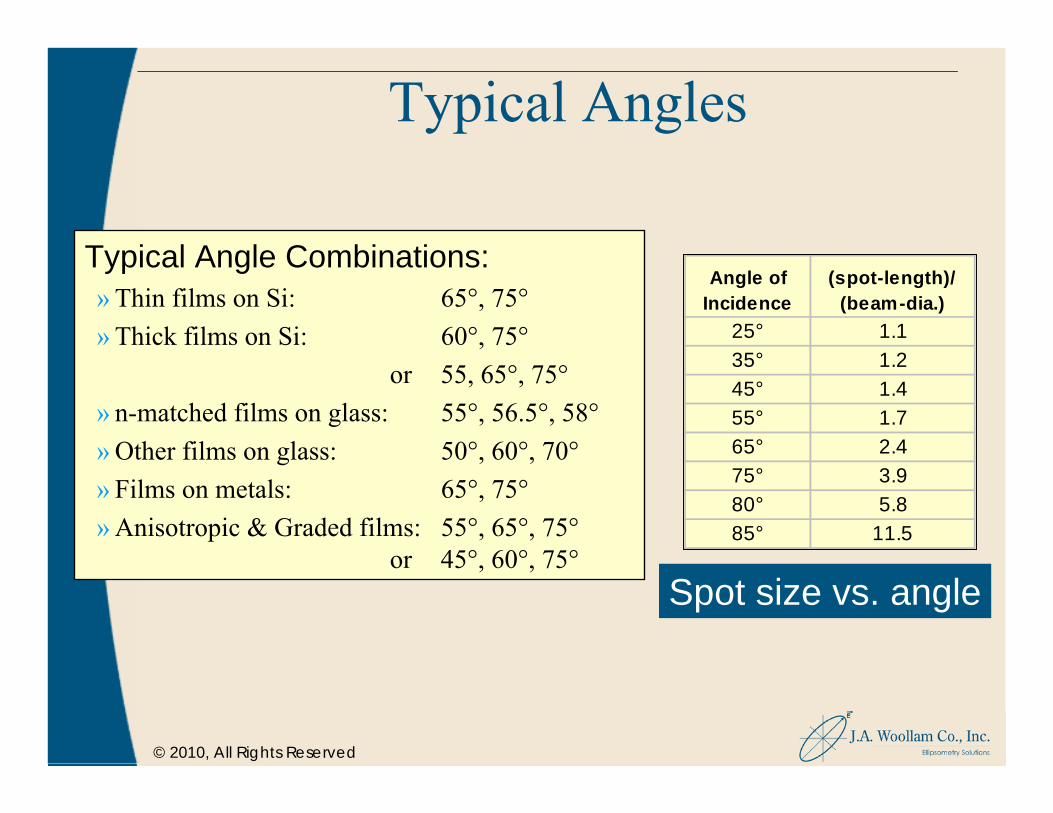
Typical Angle Combinations:» Thin films on Si: 65°, 75°» Thick films on Si: 60°, 75°
or 55, 65°, 75°» n-matched films on glass: 55°, 56.5°, 58°» Other films on glass: 50°, 60°, 70°» Films on metals: 65°, 75°» Anisotropic & Graded films: 55°, 65°, 75°
or 45°, 60°, 75°
Angle of Incidence
(spot-length)/ (beam-dia.)
25° 1.135° 1.245° 1.455° 1.765° 2.475° 3.980° 5.885° 11.5
Spot size vs. angle
Typical Angles

© 2010, All Rights Reserved
Data Analysis
Psi (Ψ)Delta (Δ)
Film ThicknessRefractive Index
Surface Roughness Interfacial Regions
CompositionCrystallinityAnisotropyUniformity
…
What Ellipsometry Measures: What we are Interested in:
Model-based analysis usuallyrequired to extract
quantities of interest!!
© 2010, All Rights Reserved
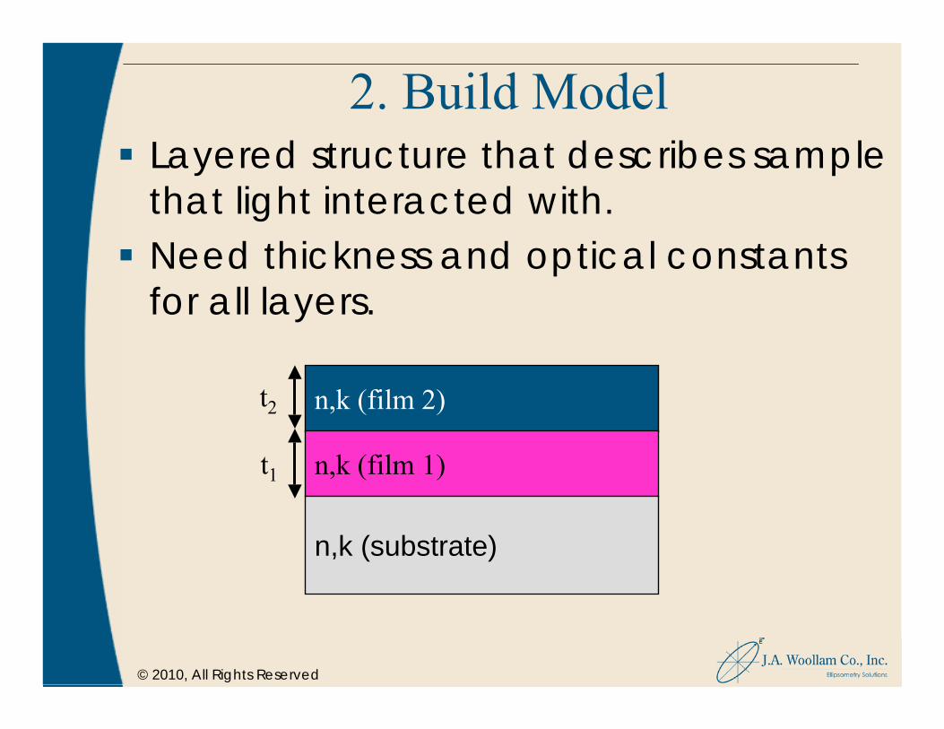
2. Build ModelLayered structure that describes sample that light interacted with.Need thickness and optical constants for all layers.
n,k (film 2)
n,k (film 1)
n,k (substrate)
t2
t1

© 2010, All Rights Reserved
Measurement/Analysis Flow Chart

© 2010, All Rights Reserved
3. Generated dataCalculate Ψ(λ,φ)/Δ(λ,φ)values of model
Compare to Experimental data– Visually &
Mathematically.
Adjust unknown (fit) parameters to get close to solution.
Generated and Experimental
Wavelength (nm)300 600 900 1200 1500 1800
Ψ in
deg
rees
0
20
40
60
80
Model Fit Exp E 70°Exp E 75°
Generated and Experimental
Wavelength (nm)300 600 900 1200 1500 1800
Ψ in
deg
rees
0
20
40
60
80
Model Fit Exp E 70°Exp E 75°

© 2010, All Rights Reserved 61
Mean Squared Error
How do we compare results?
Mean Squared Error (MSEMSE) used to quantify the difference between experimental and model-generated data.
A smaller MSE implies a better fit.MSE may be weighted by the error bars of each measurement, so noisy data are less influence.
∑= ΔΨ ⎥
⎥
⎦
⎤
⎢⎢
⎣
⎡
⎟⎟⎠
⎞⎜⎜⎝
⎛ Δ−Δ+⎟
⎟⎠
⎞⎜⎜⎝
⎛ Ψ−Ψ−
=N
i i
ii
i
ii
MNMSE
1
2
exp,
expmod2
exp,
expmod
21
σσ

© 2010, All Rights Reserved
4. Data FitThe Marquardt-Levenberg* algorithm is used to quickly find the minimum MSE.Good starting values may be important
MSE
Thickness
startingthickness(guess)
BESTFIT
Local Minima
* W.H. Press et al., Numerical Recipes in C, Cambridge, UK: Cambridge University Press, 1988.

© 2010, All Rights Reserved 63
Data Fit TypesAll vary “fit” parameters to find best agreement with Experimental Data
Normal Fit
– Works with ALL selected data simultaneously.
Global Fit
– Searches Grid of starting values.
Point-by-Point Fit
– Fit on wavelength-by-wavelength basis.

© 2010, All Rights Reserved 64
Evaluate ResultsFind the simplest optical model that fits Experimental Data.
Visually compare experimental and generated
data
How low is MSE? Can it be reduced?
Are fit parameters physical?
Check mathematical “goodness of fit” indicators
– Correlation matrix, 90% confidence limits.
© 2010, All Rights Reserved 65
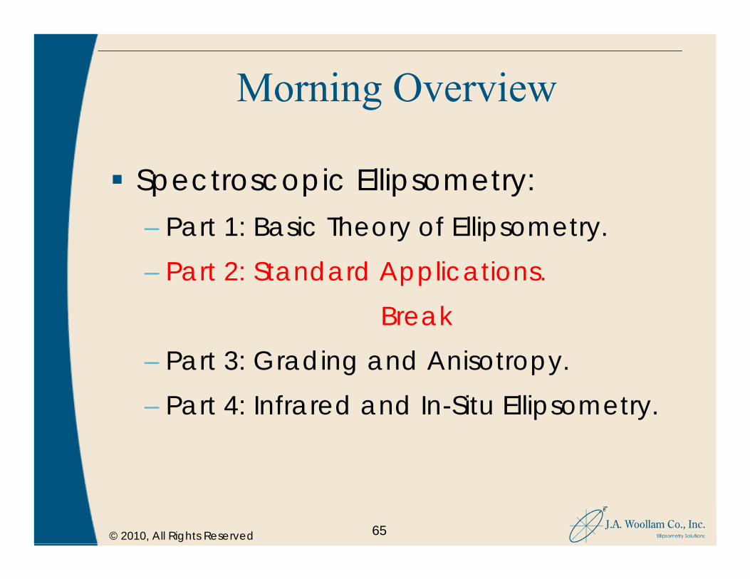
Morning Overview
Spectroscopic Ellipsometry:– Part 1: Basic Theory of Ellipsometry.– Part 2: Standard Applications.
Break– Part 3: Grading and Anisotropy.– Part 4: Infrared and In-Situ Ellipsometry.

© 2010, All Rights Reserved
Data Analysis StrategiesSubstrates
Opaque Substrates.Semiconductor substrates.Transparent substrates.
FilmsTransparent thin films.Absorbing thin films.Dispersion Models.

© 2010, All Rights Reserved
Substrate Optical Constants
Dielectrics
Semiconductors
MetalsIndex of Refraction, N
Wavelength (nm)300 600 900 1200 1500 1800
Inde
x, n
1.4
1.6
1.8
2.0
2.2
SiO2Si3N4
Silicon
Wavelength (nm)200 400 600 800 1000 1200
Inde
x of
refra
ctio
n, n
Extinction C
oefficient, k
1.0
2.0
3.0
4.0
5.0
6.0
7.0
0.0
1.0
2.0
3.0
4.0
5.0
6.0
NK
Aluminum
Wavelength (nm)0 300 600 900 1200 1500 1800
Inde
x of
refra
ctio
n, n
Extinction C
oefficient, k
0.0
0.5
1.0
1.5
2.0
2.5
3.0
0
3
6
9
12
15
18
NK
Substrate
© 2010, All Rights Reserved
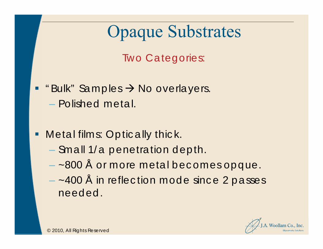
Opaque SubstratesTwo Categories:
“Bulk” Samples No overlayers.– Polished metal.
Metal films: Optically thick.– Small 1/a penetration depth. – ~800 Å or more metal becomes opque.– ~400 Å in reflection mode since 2 passes
needed.

© 2010, All Rights Reserved
Opaque SubstratesBulk Materials and Optically Thick Films
Two experimental parameters measured:– Ψ and Δ.
Two unknowns to be determined.– n and k at each wavelength.
Fit Strategy:– “Invert” psi and delta for n and k.
• Normal fit from reference values if material is known - (e.g.-bulk aluminum).
• Point by point fit from pseudo optical constants if unknown.
Examples: Optically thick Gold (Au, Al, Pt, etc).For Practice: WVASE32 Software manual.– Example #2, page 13-24. Optically thick Chromium.

© 2010, All Rights Reserved
Example: Optically Thick AluminumSimple Point-by-Point fit for n and k.
Generated and Experimental
Photon Energy (eV)0.0 1.0 2.0 3.0 4.0 5.0 6.0
Ψ in
deg
rees
38.0
39.0
40.0
41.0
42.0
43.0
44.0
45.0
Model Fit Exp E 65°Exp E 70°Exp E 75°
Generated and Experimental
Photon Energy (eV)0.0 1.0 2.0 3.0 4.0 5.0 6.0
Δ in
deg
rees
40
60
80
100
120
140
160
180
Model Fit Exp E 65°Exp E 70°Exp E 75°
Optical Constants
Wavelength (nm)0 300 600 900 1200 1500 1800
Inde
x of
refra
ctio
n 'n
'
0.0
0.5
1.0
1.5
2.0
2.5
3.0
Al, measuredAl, library
Optical Constants
Wavelength (nm)0 300 600 900 1200 1500 1800
Ext
inct
ion
Coe
ffici
ent '
k'
0
3
6
9
12
15
18
Al, measured Al, library
© 2010, All Rights Reserved
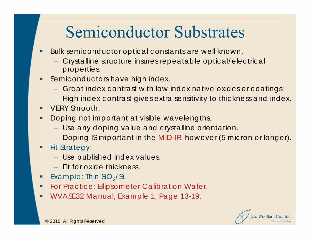
Semiconductor SubstratesBulk semiconductor optical constants are well known.– Crystalline structure insures repeatable optical/electrical
properties.Semiconductors have high index.– Great index contrast with low index native oxides or coatings!– High index contrast gives extra sensitivity to thickness and index.
VERY Smooth.Doping not important at visible wavelengths.– Use any doping value and crystalline orientation.– Doping IS important in the MID-IR, however (5 micron or longer).
Fit Strategy:– Use published index values. – Fit for oxide thickness.
Example: Thin SiO2/Si.For Practice: Ellipsometer Calibration Wafer.WVASE32 Manual, Example 1, Page 13-19.

© 2010, All Rights Reserved
Transparent SubstratesTwo Categories:
1. Uncoated Glass.2. Rigid bulk Plastic.
VERY Transparent (k=0 or very small).– Large to infinite 1/a penetration depth.– Back surface reflections may be present.
• 3 ways to handle back surface reflection:- Separate front and back beams (thick samples). - Roughen back side (grinder, sandpaper, small
sandblaster).- Model with WVASE32 back surface reflection
correction.

© 2010, All Rights Reserved
Transparent SubstratesExamples: 1 mm thick 7059, 1737, or float glass.Fit Strategy:– One unknown to be determined n(λ).– Only need one experimental parameter Ψ(λ).
Fit psi for index at each wavelength.– Cauchy fit, or– Normal fit.– Tip: Reflectance will be very low near Brewster’s
angle…so acquire data above Brewster’s angle.• Use 60°-80° for best psi data, delta will be near
zero.• Effectively a psi only fit.
For Practice: WVASE32 Software manual.– Example #4, page 13-31. Glass Cover slip.

© 2010, All Rights Reserved
Cauchy Describes index (n) of transparentmaterials (k=0). “Normal Dispersion”.
n(λ)=A+B/λ2+C/λ4
k(λ)=0
Wavelength (nm)200 400 600 800 1000 1200
Inde
x of
refra
ctio
n 'n
'
1.44
1.47
1.50
1.53
1.56
1.59
1.62
1.65A sets amplitude
B and C give dispersion shape

© 2010, All Rights Reserved
Transparent SubstratesObtain Error Bars on index.– Perform both Cauchy and normal fits.– Compare them!…great way to obtain error bars
at each wavelength.– Cauchy gives smooth average.– Normal fit gives measured error.
Glass Optical Constants: Comparison
Wavelength (nm)300 600 900 1200 1500 1800
Inde
x of
refra
ctio
n 'n
'
1.510
1.515
1.520
1.525
1.530
1.535
1.540
1.545
Cauchy FitNormal Fit

© 2010, All Rights Reserved
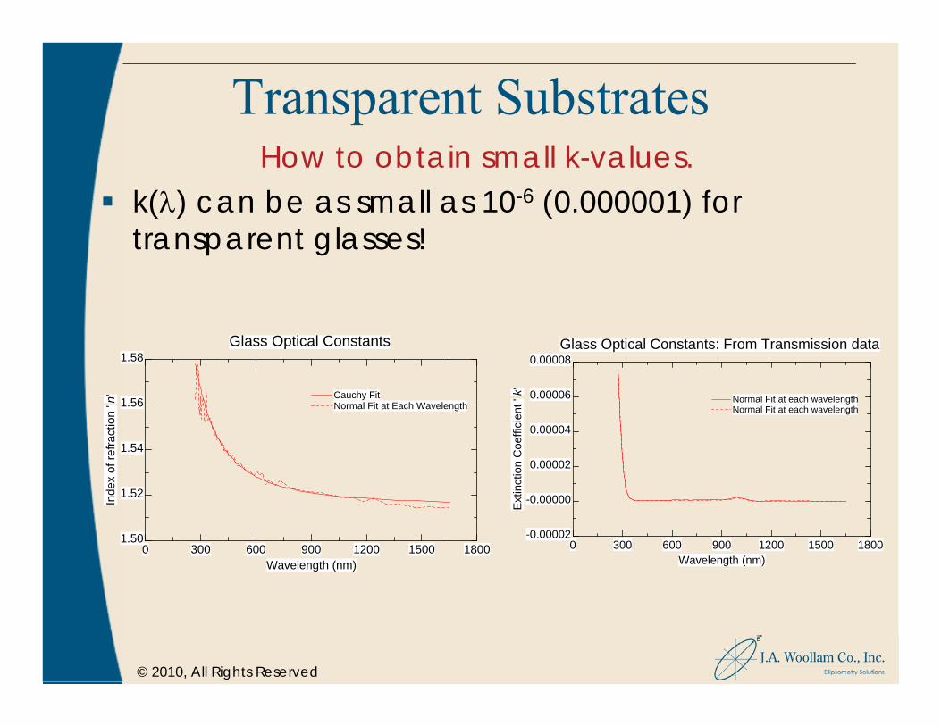
Transparent SubstratesHow to obtain small k-values.
k(λ) can be as small as 10-6 (0.000001) for transparent glasses!– NOT seen in reflection mode. (no path length.)– Increase path length with transmission data.– EASY to see small k-values with transmission data.
Generated and Experimental
Wavelength (nm)0 300 600 900 1200 1500 1800
Ψ in
deg
rees
0
10
20
30
40
Model Fit Exp Eb 60°Exp Eb 70°Exp Eb 80°
Generated and Experimental
Wavelength (nm)0 300 600 900 1200 1500 1800
Tran
smis
sion
0.0
0.2
0.4
0.6
0.8
1.0
Model Fit Exp pT 0°
© 2010, All Rights Reserved
Transparent SubstratesHow to obtain small k-values.
k(λ) can be as small as 10-6 (0.000001) for transparent glasses!
Glass Optical Constants
Wavelength (nm)0 300 600 900 1200 1500 1800
Inde
x of
refra
ctio
n 'n
'
1.50
1.52
1.54
1.56
1.58
Cauchy FitNormal Fit at Each Wavelength
Glass Optical Constants: From Transmission data
Wavelength (nm)0 300 600 900 1200 1500 1800
Ext
inct
ion
Coe
ffici
ent '
k'-0.00002
-0.00000
0.00002
0.00004
0.00006
0.00008
Normal Fit at each wavelengthNormal Fit at each wavelength

© 2010, All Rights Reserved
Transparent SubstratesSoda-Lime Glass
5 mm thick Soda-Lime glass:
VERY important to know substrate absorption if fitting transmission data for thin films.
Soda-Lime Glass Optical Constants
Wavelength (nm)300 600 900 1200 1500 1800
Inde
x of
refra
ctio
n 'n
'
Extinction C
oefficient 'k'
1.490
1.500
1.510
1.520
1.530
1.540
1.550
0.0E+000
5.0E-006
1.0E-005
1.5E-005
2.0E-005
2.5E-005
nk
Experimental Data: 5 mm thick Soda-Lime Glass
Wavelength (nm)300 600 900 1200 1500 1800
Tran
smis
sion
0.0
0.2
0.4
0.6
0.8
1.0
Exp pT 0°

© 2010, All Rights Reserved
Transparent FilmsSensitivity comes from INDEX DIFFERENCEbetween layers = Stronger reflections.High index difference gives greater sensitivity:– Smaller error bars on thickness and index, OR– More layers!...Hi-Lo stack optical filters.
Fit refractive index with Cauchy equation.Tip: For greatest sensitivity, maximize the index difference between adjacent layers.
For Practice: WVASE32 Software manual.– Example #5, page 13-38. Organic film on
Silicon.

© 2010, All Rights Reserved
Absorbing FilmsThin Film Data Analysis – Organic and Polymer Thin Films.
• Resists, AR coatings, pellicles.– Semiconductor Thin Films.
• Point-by-Point versus Dispersion Models.• Alloy ratio models.• Surface oxides and roughness.• Dispersion Models.
– Metal and Opaque Thin Films.• Thin metal on glass?…Add transmission
data.• Thin metal film on thick SiO2 on Silicon.

© 2010, All Rights Reserved
UV Absorbing FilmsTransparent films with onset of absorption in UV: Si3N4, SiON, Resists, Organics, etc.
Wavelength (nm)0 300 600 900 1200 1500 1800
Inde
x of
refra
ctio
n ' n
' Extinction Coefficient ' k
'
0.9
1.2
1.5
1.8
2.1
2.4
2.7
0.0
0.3
0.6
0.9
1.2
1.5
n
k
Experimental Data
Wavelength (nm)0 300 600 900 1200 1500 1800
Ψ in
deg
rees
0
10
20
30
40
50
Exp E 70°Exp E 75°

© 2010, All Rights Reserved
UV Absorbing Films
Divide analysis into 2 parts:Step 1: Transparent Region.– Range select data where film is transparent (k=0)
• typically longer wavelengths.– Two unknowns n(λ) & thickness.– Two measured parameters Ψ(λ) & Δ(λ).– Cauchy fit n(λ) & thickness
Step 2: Absorbing Region.– Fix thickness from Step 1.– Fit n/k on a wavelength-by-wavelength basis.– “Point by Point Fit.”

83© 2010, All Rights Reserved
Step 1: Cauchy fitCauchy fit at long wavelengths determines thickness
Wavelength in nm
0 200 400 600 800 1000 1200 1400
Inde
x of
refra
ctio
n 'n
'
Extinction C
oefficient 'k'
1.40
1.50
1.60
1.70
1.80
0.00
0.05
0.10
0.15
0.20
0.25
nk
Cauchy only valid in transparent region
© 2010, All Rights Reserved
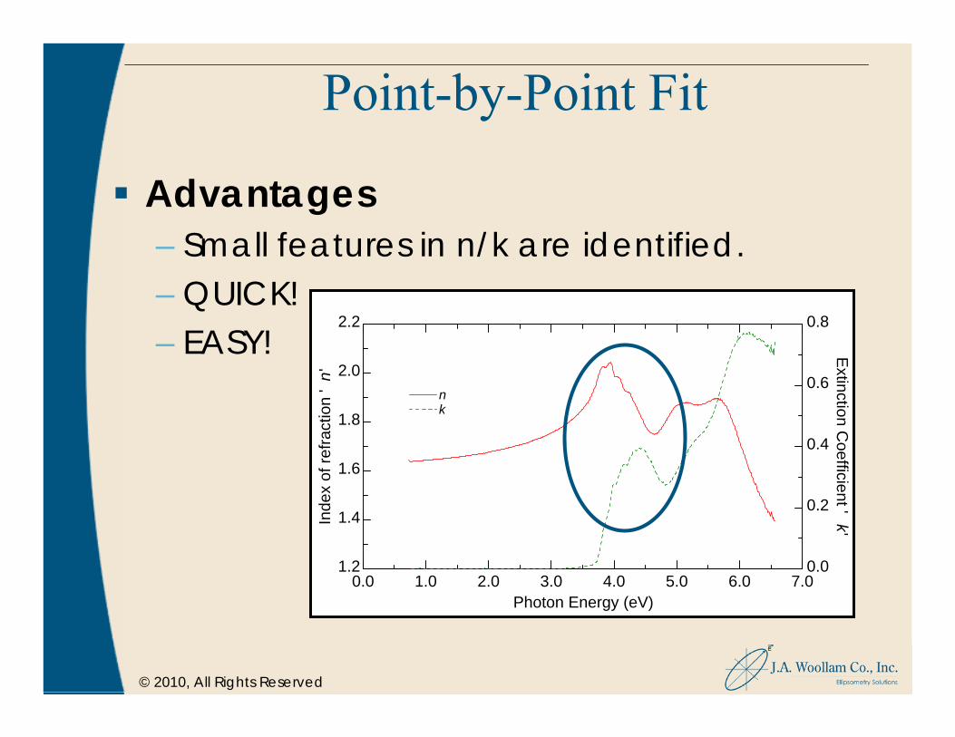
Advantages– Small features in n/k are identified.– QUICK!– EASY!
Photon Energy (eV)0.0 1.0 2.0 3.0 4.0 5.0 6.0 7.0
Inde
x of
refra
ctio
n '
n'
Extinction C
oefficient 'k'
1.2
1.4
1.6
1.8
2.0
2.2
0.0
0.2
0.4
0.6
0.8
nk
Point-by-Point Fit

© 2010, All Rights Reserved
Point-by-Point FitsAdvantages– QUICK!– EASY!– Capture small features.
Disadvantages– Not necessarily KK
consistent. Noise can be present.
85
Photon Energy (eV)0.0 1.0 2.0 3.0 4.0 5.0 6.0 7.0
Inde
x of
refra
ctio
n '
n'E
xtinction Coefficient '
k'
1.2
1.4
1.6
1.8
2.0
2.2
0.0
0.2
0.4
0.6
0.8
nk

© 2010, All Rights Reserved
Semiconductor Thin Film: ZnS on SiZinc Sulfide on Silicon
• Fit to Cauchy model over limited spectral range (0.73 to 3eV)
• Include surface layer, optical constants obtained from separate sample that had been annealed.
• Add index grading.• Point-by-point fit n and k over
entire spectral range. • Small glitches in Pt-by-Pt
optical constants. Can use them to set up dispersion model.
0 si_jaw 1 mm1 zns_nk 0 Å2 graded (zns_nk)/void 3328.9 Å3 zns surface layer_l 34.449 Å
Optical Constants
Photon Energy (eV)0.0 1.0 2.0 3.0 4.0 5.0 6.0 7.0
Inde
x of
refra
ctio
n 'n
'
Extinction C
oefficient 'k'
2.2
2.4
2.6
2.8
3.0
3.2
3.4
3.6
0.0
0.3
0.6
0.9
1.2
1.5
1.8
nk
Small glitches are not physical
© 2010, All Rights Reserved
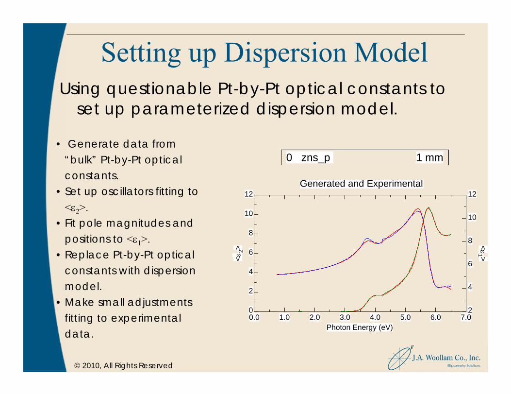
Setting up Dispersion Model Using questionable Pt-by-Pt optical constants to
set up parameterized dispersion model.
• Generate data from “bulk” Pt-by-Pt optical constants.
• Set up oscillators fitting to<ε2>.
• Fit pole magnitudes and positions to <ε1>.
• Replace Pt-by-Pt optical constants with dispersion model.
• Make small adjustments fitting to experimental data.
Generated and Experimental
Photon Energy (eV)0.0 1.0 2.0 3.0 4.0 5.0 6.0 7.0
<ε2>
<ε1 >
0
2
4
6
8
10
12
2
4
6
8
10
12
0 zns_p 1 mm

© 2010, All Rights Reserved
Absorbing Thin Films: Dispersion Models
Advantages:– Correct surface layer optical constants not as
critical.– Fit to all the data simultaneously.
• Sensitive to all parameters at once. Regions of spectrum are more sensitive to certain parameters that others are not.
– More Flexibility.
Disadvantages:– Setting up dispersion model can be rigorous.– Can miss small details in optical constants.

© 2010, All Rights Reserved 89
Procedure for Absorbing Films1. Cauchy Fit
– transparent region only2. Pt-by-Pt Fit – all wavelengths
– fix thickness– Save tabulated n & k values– Replace Cauchy with Genosc
3. Match n,k using Genosc– Load tabulated file from pt-by-pt fit into
Reference– fit reference – first e2, then e1
4. Fit Ψ & Δ data using new Genosc model

© 2010, All Rights Reserved
Compound Semiconductor FilmsAlloy Semiconductors:
AlGaAs, InGaAs, HgCdTe, etc.Use alloy material files. Fit for alloy ratio.– Critical points shifted automatically with alloy
fraction!
For Practice: WVASE32 Software manual.– Example #10, page 13-71.
GaAs/AlGaAs/GaAs wafer.

© 2010, All Rights Reserved
Alloy Ratio Model: AlxGa1-xAs Multilayer
• Superlattice model allows coupling layers together.
• Fit alloy ratios and thicknesses.
• Many fit parameters but do not appear to be correlated.
Different alloy ratios produces different optical constants. Alloy ratios models allow adjustment of optical constants with a single parameter (x).
B. Johs, et al., “Overview of Variable Angle Spectroscopic Ellipsometry (VASE), Part I: Basic Theory and Typical Applications” SPIE Proc. Vol CR72, (1999) pp. 50-51.

© 2010, All Rights Reserved
Thin Metal Films on GlassSemitransparent Ag on Quartz substrate– Adding Transmission intensity data breaks
correlation between optical constants and thickness.
– Ag optical constants can be fit at each measured wavelength, or modeled with summation of Drude and several Lorentz oscillators.
For Practice: WVASE32 Software manual.– Example #7, page 13-51. Thin Silver on Fused
Silica.

© 2010, All Rights Reserved
Thin Metal Film on GlassResults: 300 Å Silver on Fused Silica.
Generated and Experimental
Wavelength (nm)300 600 900 1200 1500 1800
Ψ in
deg
rees
10
20
30
40
50
Model Fit Exp E 65°Exp E 70°Exp E 75°
Generated and Experimental
Wavelength (nm)300 600 900 1200 1500 1800
Δ in
deg
rees
0
30
60
90
120
150
180
Model Fit Exp E 65°Exp E 70°Exp E 75°
Generated and Experimental
Wavelength (nm)300 600 900 1200 1500 1800
Tran
smis
sion
0.0
0.2
0.4
0.6
0.8
Model Fit Exp pT 0°
0 sio2 1 mm1 ag 341.7 Å2 srough 7.4 Å
Silver Optical Constants
Wavelength (nm)300 600 900 1200 1500 1800
Inde
x of
refra
ctio
n 'n
'
Extinction C
oefficient 'k'
0.0
0.3
0.6
0.9
1.2
1.5
1.8
0
2
4
6
8
10
12
14
nk
© 2010, All Rights Reserved
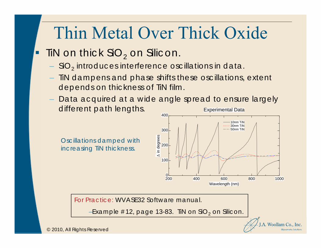
Thin Metal Over Thick OxideTiN on thick SiO2 on Silicon.– SiO2 introduces interference oscillations in data.– TiN dampens and phase shifts these oscillations, extent
depends on thickness of TiN film.– Data acquired at a wide angle spread to ensure largely
different path lengths. Experimental Data
Wavelength (nm)200 400 600 800 1000
Δ in
deg
rees
0
100
200
300
400
10nm TiN30nm TiN50nm TiN
Oscillations damped with increasing TiN thickness.
For Practice: WVASE32 Software manual.
–Example #12, page 13-83. TiN on SiO2 on Silicon.

© 2010, All Rights Reserved
Thin Metal on Thick Oxide
0 si_jaw 1 mm1 sio2_jaw 627.46 nm2 tin_l 55.128 nm
Generated and Experimental
Wavelength (nm)200 400 600 800 1000
Ψ in
deg
rees
10
15
20
25
30
35
40
45
Model Fit Exp E 50°Exp E 60°Exp E 70°Exp E 80°
Generated and Experimental
Wavelength (nm)200 400 600 800 1000
Δ in
deg
rees
0
30
60
90
120
150
180
Model Fit Exp E 50°Exp E 60°Exp E 70°Exp E 80°
tin_l Optical Constants
Wavelength (nm)200 400 600 800 1000
Inde
x of
refra
ctio
n 'n
'E
xtinction Coefficient 'k'
1.2
1.4
1.6
1.8
2.0
2.2
2.4
2.6
1.0
2.0
3.0
4.0
5.0
nk
Results: TiN on SiO2 on Silicon.

© 2010, All Rights Reserved
Break!!