operational amplifiers - wbuthelp.comoperational amplifiers contents 8.1 introduction 8.2...
TRANSCRIPT

OPERATIONAL AMPLIFIERS
Contents
8.1 Introduction
8.2 Single-ended and differential amplifiers
8.3 The ”operational” amplifier
8.4 Negative feedback
8.5 Divided feedback
8.6 An analogy for divided feedback
8.7 Voltage-to-current signal conversion
8.8 Averager and summer circuits
8.9 Building a differential amplifier
8.10 The instrumentation amplifier
8.11 Differentiator and integrator circuits
8.12 Positive feedback
8.13 Practical considerations
8.13.1 Common-mode gain
8.13.2 Offset voltage
8.13.3 Bias current
8.13.4 Drift
8.13.5 Frequency response
8.13.6 Input to output phase shift
8.14 Operational amplifier models
8.15 Data
8.1 Introduction
The operational amplifier is arguably the most useful singlecuitry. With only a handful of external components, it can be
mywbut.com
1

of analog signal processing tasks. It is also quite affordable, most general-purpose amplifiersselling for under a dollar apiece. Modern designs have been engineered with durability inmind as well: several ”op-amps” are manufactured that can sustain direct short-circuits ontheir outputs without damage.
One key to the usefulness of these little circuits is in the engineering principle of feedback,particularly negative feedback, which constitutes the foundation of almost all automatic controlprocesses. The principles presented here in operational amplifier circuits, therefore, extendwell beyond the immediate scope of electronics. It is well worth the electronics student’s timeto learn these principles and learn them well.
8.2 Single-ended and differential amplifiers
For ease of drawing complex circuit diagrams, electronic amplifiers are often symbolized by asimple triangle shape, where the internal components are not individually represented. Thissymbology is very handy for cases where an amplifier’s construction is irrelevant to the greaterfunction of the overall circuit, and it is worthy of familiarization:
Input Output
+Vsupply
-Vsupply
General amplifier circuit symbol
The +V and -V connections denote the positive and negative sides of the DC power supply,respectively. The input and output voltage connections are shown as single conductors, becauseit is assumed that all signal voltages are referenced to a common connection in the circuit calledground. Often (but not always!), one pole of the DC power supply, either positive or negative,is that ground reference point. A practical amplifier circuit (showing the input voltage source,load resistance, and power supply) might look like this:
Rload
Vinput
Input Output
+V
-V
30 V+
-
Without having to analyze the actual transistor design of the amplifier, you can readilydiscern the whole circuit’s function: to take an input signal (Vin), amplify it, and drive a load
mywbut.com
2

resistance (Rload). To complete the above schematic, it would be good to specify the gains ofthat amplifier (AV , AI , AP ) and the Q (bias) point for any needed mathematical analysis.If it is necessary for an amplifier to be able to output true AC voltage (reversing polarity)
to the load, a split DC power supply may be used, whereby the ground point is electrically”centered” between +V and -V. Sometimes the split power supply configuration is referred toas a dual power supply.
Rload
Vinput
Input Output
+V
-V
+
-
+
-
15 V
15 V
The amplifier is still being supplied with 30 volts overall, but with the split voltage DCpower supply, the output voltage across the load resistor can now swing from a theoreticalmaximum of +15 volts to -15 volts, instead of +30 volts to 0 volts. This is an easy way toget true alternating current (AC) output from an amplifier without resorting to capacitive orinductive (transformer) coupling on the output. The peak-to-peak amplitude of this amplifier’soutput between cutoff and saturation remains unchanged.By signifying a transistor amplifier within a larger circuit with a triangle symbol, we ease
the task of studying and analyzing more complex amplifiers and circuits. One of these morecomplex amplifier types that we’ll be studying is called the differential amplifier. Unlike nor-mal amplifiers, which amplify a single input signal (often called single-ended amplifiers), differ-ential amplifiers amplify the voltage difference between two input signals. Using the simplifiedtriangle amplifier symbol, a differential amplifier looks like this:
−
+
Input1
Input2
+Vsupply
-Vsupply
Output
Differential amplifier
The two input leads can be seen on the left-hand side of the triangular amplifier symbol, theoutput lead on the right-hand side, and the +V and -V power supply leads on top and bottom.As with the other example, all voltages are referenced to the circuit’s ground point. Notice thatone input lead is marked with a (-) and the other is marked with a (+). Because a differentialamplifier amplifies the difference in voltage between the two inputs, each input influences the
mywbut.com
3

output voltage in opposite ways. Consider the following table of input/output voltages for adifferential amplifier with a voltage gain of 4:
Output
(-) Input1
(+) Input2
0
0
0
0 0 0 1 2.5 7
0 0 01 2.5 7
4 10 28 -4 -10 -28
3
3
-3
3
0 24
-2
-7
-20
Voltage output equation: Vout = AV(Input2 - Input1)
orVout = AV(Input(+) - Input(-))
An increasingly positive voltage on the (+) input tends to drive the output voltage morepositive, and an increasingly positive voltage on the (-) input tends to drive the output voltagemore negative. Likewise, an increasingly negative voltage on the (+) input tends to drive theoutput negative as well, and an increasingly negative voltage on the (-) input does just theopposite. Because of this relationship between inputs and polarities, the (-) input is commonlyreferred to as the inverting input and the (+) as the noninverting input.
It may be helpful to think of a differential amplifier as a variable voltage source controlledby a sensitive voltmeter, as such:
G
-
+
+V
-V
-
+
Bear in mind that the above illustration is only amodel to aid in understanding the behav-ior of a differential amplifier. It is not a realistic schematic of its actual design. The ”G” symbolrepresents a galvanometer, a sensitive voltmeter movement. The potentiometer connected be-tween +V and -V provides a variable voltage at the output pin (with reference to one side ofthe DC power supply), that variable voltage set by the reading of the galvanometer. It must beunderstood that any load powered by the output of a differential amplifier gets its current fromthe DC power source (battery), not the input signal. The input signal (to the galvanometer)merely controls the output.
This concept may at first be confusing to students new to amplifiers. With all these polar-ities and polarity markings (- and +) around, its easy to get confused and not know what theoutput of a differential amplifier will be. To address this potential confusion, here’s a simplerule to remember:
mywbut.com
4

−
+Differential
input voltage
-
+
+
-Outputvoltage
Differentialinput voltage
-
+ −
++
-voltageOutput
When the polarity of the differential voltage matches the markings for inverting and nonin-verting inputs, the output will be positive. When the polarity of the differential voltage clasheswith the input markings, the output will be negative. This bears some similarity to the math-ematical sign displayed by digital voltmeters based on input voltage polarity. The red test leadof the voltmeter (often called the ”positive” lead because of the color red’s popular associationwith the positive side of a power supply in electronic wiring) is more positive than the black,the meter will display a positive voltage figure, and vice versa:
Differentialinput voltage
-
+
Differentialinput voltage
-
+
6 V
6 V
-
+
-
+red
blk
blk
red
Digital Voltmeter
Digital Voltmeter
+ 6.00 V
- 6.00 V
Just as a voltmeter will only display the voltage between its two test leads, an ideal differ-ential amplifier only amplifies the potential difference between its two input connections, notthe voltage between any one of those connections and ground. The output polarity of a differ-ential amplifier, just like the signed indication of a digital voltmeter, depends on the relativepolarities of the differential voltage between the two input connections.If the input voltages to this amplifier represented mathematical quantities (as is the case
within analog computer circuitry), or physical process measurements (as is the case withinanalog electronic instrumentation circuitry), you can see how a device such as a differentialamplifier could be very useful. We could use it to compare two quantities to see which isgreater (by the polarity of the output voltage), or perhaps we could compare the differencebetween two quantities (such as the level of liquid in two tanks) and flag an alarm (based on theabsolute value of the amplifier output) if the difference became too great. In basic automaticcontrol circuitry, the quantity being controlled (called the process variable) is compared witha target value (called the setpoint), and decisions are made as to how to act based on thediscrepancy between these two values. The first step in electronically controlling such a scheme
mywbut.com
5

is to amplify the difference between the process variable and the setpoint with a differentialamplifier. In simple controller designs, the output of this differential amplifier can be directlyutilized to drive the final control element (such as a valve) and keep the process reasonablyclose to setpoint.
• REVIEW:
• A ”shorthand” symbol for an electronic amplifier is a triangle, the wide end signifyingthe input side and the narrow end signifying the output. Power supply lines are oftenomitted in the drawing for simplicity.
• To facilitate true AC output from an amplifier, we can use what is called a split or dualpower supply, with two DC voltage sources connected in series with the middle pointgrounded, giving a positive voltage to ground (+V) and a negative voltage to ground (-V).Split power supplies like this are frequently used in differential amplifier circuits.
• Most amplifiers have one input and one output. Differential amplifiers have two inputsand one output, the output signal being proportional to the difference in signals betweenthe two inputs.
• The voltage output of a differential amplifier is determined by the following equation:Vout = AV (Vnoninv - Vinv)
8.3 The ”operational” amplifier
Long before the advent of digital electronic technology, computers were built to electronicallyperform calculations by employing voltages and currents to represent numerical quantities.This was especially useful for the simulation of physical processes. A variable voltage, for in-stance, might represent velocity or force in a physical system. Through the use of resistivevoltage dividers and voltage amplifiers, the mathematical operations of division and multipli-cation could be easily performed on these signals.The reactive properties of capacitors and inductors lend themselves well to the simulation
of variables related by calculus functions. Remember how the current through a capacitorwas a function of the voltage’s rate of change, and how that rate of change was designatedin calculus as the derivative? Well, if voltage across a capacitor were made to represent thevelocity of an object, the current through the capacitor would represent the force required toaccelerate or decelerate that object, the capacitor’s capacitance representing the object’s mass:
iC = C dvdt
F = m dvdt
Where, Where,
iC =
C =
dvdt
=
Instantaneous current through capacitorCapacitance in farads
Rate of change of voltage over time
F =
m =
dvdt
=
Force applied to object
Mass of object
Rate of change of velocity over time
mywbut.com
6

This analog electronic computation of the calculus derivative function is technically knownas differentiation, and it is a natural function of a capacitor’s current in relation to the voltageapplied across it. Note that this circuit requires no ”programming” to perform this relativelyadvanced mathematical function as a digital computer would.
Electronic circuits are very easy and inexpensive to create compared to complex physicalsystems, so this kind of analog electronic simulation was widely used in the research anddevelopment of mechanical systems. For realistic simulation, though, amplifier circuits of highaccuracy and easy configurability were needed in these early computers.
It was found in the course of analog computer design that differential amplifiers with ex-tremely high voltage gains met these requirements of accuracy and configurability better thansingle-ended amplifiers with custom-designed gains. Using simple components connected tothe inputs and output of the high-gain differential amplifier, virtually any gain and any func-tion could be obtained from the circuit, overall, without adjusting or modifying the internalcircuitry of the amplifier itself. These high-gain differential amplifiers came to be known asoperational amplifiers, or op-amps, because of their application in analog computers’ mathe-matical operations.
Modern op-amps, like the popular model 741, are high-performance, inexpensive integratedcircuits. Their input impedances are quite high, the inputs drawing currents in the range ofhalf a microamp (maximum) for the 741, and far less for op-amps utilizing field-effect inputtransistors. Output impedance is typically quite low, about 75 Ω for the model 741, and manymodels have built-in output short circuit protection, meaning that their outputs can be directlyshorted to ground without causing harm to the internal circuitry. With direct coupling betweenop-amps’ internal transistor stages, they can amplify DC signals just as well as AC (up tocertain maximum voltage-risetime limits). It would cost far more in money and time to designa comparable discrete-transistor amplifier circuit to match that kind of performance, unlesshigh power capability was required. For these reasons, op-amps have all but obsoleted discrete-transistor signal amplifiers in many applications.
The following diagram shows the pin connections for single op-amps (741 included) whenhoused in an 8-pin DIP (Dual Inline Package) integrated circuit:
mywbut.com
7
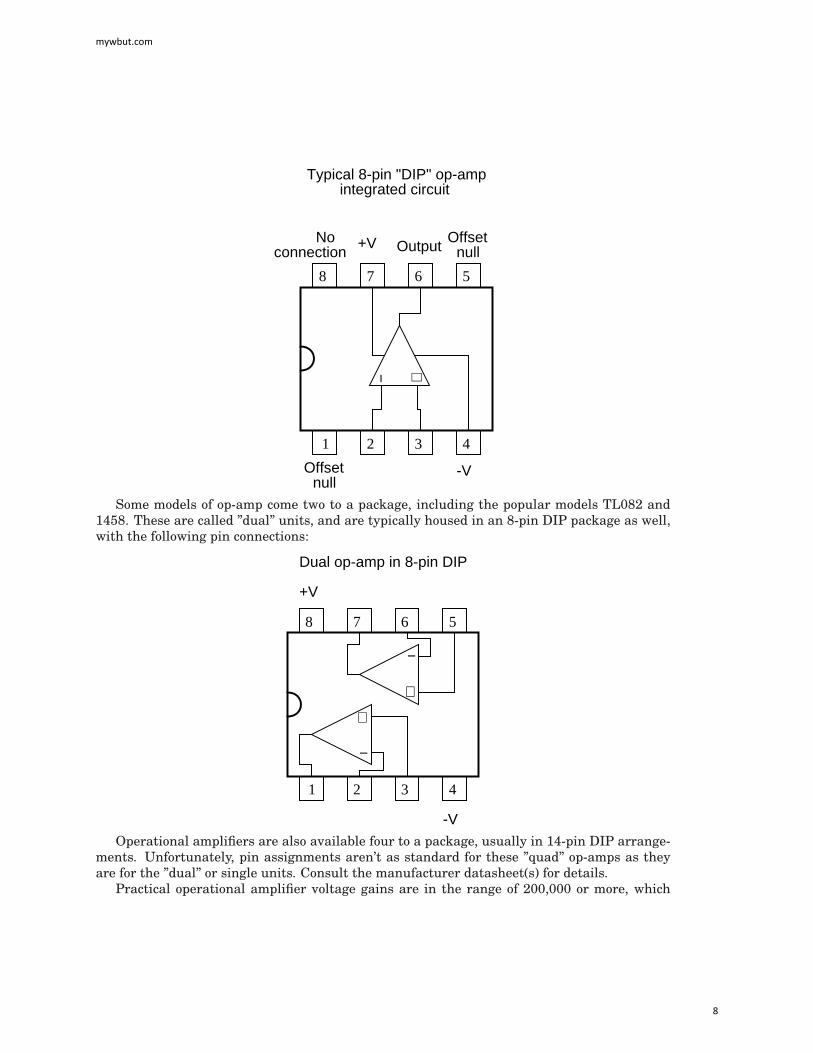
Typical 8-pin "DIP" op-ampintegrated circuit
8 7 6
1 2 3 4
5
− +
+V
-V
OutputNo
connectionOffset
null
Offsetnull
Some models of op-amp come two to a package, including the popular models TL082 and1458. These are called ”dual” units, and are typically housed in an 8-pin DIP package as well,with the following pin connections:
8 7 6
1 2 3 4
5
Dual op-amp in 8-pin DIP
+V
-V
−
+
−
+
Operational amplifiers are also available four to a package, usually in 14-pin DIP arrange-ments. Unfortunately, pin assignments aren’t as standard for these ”quad” op-amps as theyare for the ”dual” or single units. Consult the manufacturer datasheet(s) for details.Practical operational amplifier voltage gains are in the range of 200,000 or more, which
mywbut.com
8

makes them almost useless as an analog differential amplifier by themselves. For an op-ampwith a voltage gain (AV ) of 200,000 and a maximum output voltage swing of +15V/-15V, allit would take is a differential input voltage of 75 µV (microvolts) to drive it to saturation orcutoff! Before we take a look at how external components are used to bring the gain down to areasonable level, let’s investigate applications for the ”bare” op-amp by itself.
One application is called the comparator. For all practical purposes, we can say that theoutput of an op-amp will be saturated fully positive if the (+) input is more positive than the (-)input, and saturated fully negative if the (+) input is less positive than the (-) input. In otherwords, an op-amp’s extremely high voltage gain makes it useful as a device to compare twovoltages and change output voltage states when one input exceeds the other in magnitude.
−
+
+V
-V
LEDVin
In the above circuit, we have an op-amp connected as a comparator, comparing the inputvoltage with a reference voltage set by the potentiometer (R1). If Vin drops below the voltageset by R1, the op-amp’s output will saturate to +V, thereby lighting up the LED. Otherwise, ifVin is above the reference voltage, the LED will remain off. If Vin is a voltage signal producedby a measuring instrument, this comparator circuit could function as a ”low” alarm, with thetrip-point set by R1. Instead of an LED, the op-amp output could drive a relay, a transistor, anSCR, or any other device capable of switching power to a load such as a solenoid valve, to takeaction in the event of a low alarm.
Another application for the comparator circuit shown is a square-wave converter. Supposethat the input voltage applied to the inverting (-) input was an AC sine wave rather than astable DC voltage. In that case, the output voltage would transition between opposing statesof saturation whenever the input voltage was equal to the reference voltage produced by thepotentiometer. The result would be a square wave:
mywbut.com
9

−
+
+V
-V
VoutVin
Vin Vout
Adjustments to the potentiometer setting would change the reference voltage applied tothe noninverting (+) input, which would change the points at which the sine wave would cross,changing the on/off times, or duty cycle of the square wave:
−
+
+V
-V
VoutVin
Vin Vout
It should be evident that the AC input voltage would not have to be a sine wave in particularfor this circuit to perform the same function. The input voltage could be a triangle wave,sawtooth wave, or any other sort of wave that ramped smoothly from positive to negative topositive again. This sort of comparator circuit is very useful for creating square waves ofvarying duty cycle. This technique is sometimes referred to as pulse-width modulation, orPWM (varying, or modulating a waveform according to a controlling signal, in this case thesignal produced by the potentiometer).
Another comparator application is that of the bargraph driver. If we had several op-amps
mywbut.com
10

connected as comparators, each with its own reference voltage connected to the inverting input,but each one monitoring the same voltage signal on their noninverting inputs, we could build abargraph-style meter such as what is commonly seen on the face of stereo tuners and graphicequalizers. As the signal voltage (representing radio signal strength or audio sound level)increased, each comparator would ”turn on” in sequence and send power to its respective LED.With each comparator switching ”on” at a different level of audio sound, the number of LED’silluminated would indicate how strong the signal was.
−
+
−
+
−
+
−
+
+V
-V
Vin
-V
LED1
LED2
LED3
LED4
Simple bargraph driver circuit
In the circuit shown above, LED1 would be the first to light up as the input voltage increasedin a positive direction. As the input voltage continued to increase, the other LED’s wouldilluminate in succession, until all were lit.This very same technology is used in some analog-to-digital signal converters, namely the
flash converter, to translate an analog signal quantity into a series of on/off voltages represent-ing a digital number.
• REVIEW:
• A triangle shape is the generic symbol for an amplifier circuit, the wide end signifyingthe input and the narrow end signifying the output.
• Unless otherwise specified, all voltages in amplifier circuits are referenced to a commonground point, usually connected to one terminal of the power supply. This way, we canspeak of a certain amount of voltage being ”on” a single wire, while realizing that voltageis always measured between two points.
mywbut.com
11

• A differential amplifier is one amplifying the voltage difference between two signal inputs.In such a circuit, one input tends to drive the output voltage to the same polarity of theinput signal, while the other input does just the opposite. Consequently, the first input iscalled the noninverting (+) input and the second is called the inverting (-) input.
• An operational amplifier (or op-amp for short) is a differential amplifier with an extremelyhigh voltage gain (AV = 200,000 or more). Its name hails from its original use in analogcomputer circuitry (performing mathematical operations).
• Op-amps typically have very high input impedances and fairly low output impedances.
• Sometimes op-amps are used as signal comparators, operating in full cutoff or saturationmode depending on which input (inverting or noninverting) has the greatest voltage.Comparators are useful in detecting ”greater-than” signal conditions (comparing one tothe other).
• One comparator application is called the pulse-width modulator, and is made by compar-ing a sine-wave AC signal against a DC reference voltage. As the DC reference voltageis adjusted, the square-wave output of the comparator changes its duty cycle (positiveversus negative times). Thus, the DC reference voltage controls, or modulates the pulsewidth of the output voltage.
8.4 Negative feedback
If we connect the output of an op-amp to its inverting input and apply a voltage signal tothe noninverting input, we find that the output voltage of the op-amp closely follows thatinput voltage (I’ve neglected to draw in the power supply, +V/-V wires, and ground symbol forsimplicity):
−
+Vin
Vout
As Vin increases, Vout will increase in accordance with the differential gain. However, asVout increases, that output voltage is fed back to the inverting input, thereby acting to decreasethe voltage differential between inputs, which acts to bring the output down. What will happenfor any given voltage input is that the op-amp will output a voltage very nearly equal to Vin,but just low enough so that there’s enough voltage difference left between Vin and the (-) inputto be amplified to generate the output voltage.The circuit will quickly reach a point of stability (known as equilibrium in physics), where
the output voltage is just the right amount to maintain the right amount of differential, whichin turn produces the right amount of output voltage. Taking the op-amp’s output voltage andcoupling it to the inverting input is a technique known as negative feedback, and it is the keyto having a self-stabilizing system (this is true not only of op-amps, but of any dynamic systemin general). This stability gives the op-amp the capacity to work in its linear (active) mode, as
mywbut.com
12

opposed to merely being saturated fully ”on” or ”off” as it was when used as a comparator, withno feedback at all.Because the op-amp’s gain is so high, the voltage on the inverting input can be maintained
almost equal to Vin. Let’s say that our op-amp has a differential voltage gain of 200,000. If Vin
equals 6 volts, the output voltage will be 5.999970000149999 volts. This creates just enoughdifferential voltage (6 volts - 5.999970000149999 volts = 29.99985 µV) to cause 5.999970000149999volts to be manifested at the output terminal, and the system holds there in balance. As youcan see, 29.99985 µV is not a lot of differential, so for practical calculations, we can assumethat the differential voltage between the two input wires is held by negative feedback exactlyat 0 volts.
−
+
6 V
5.999970000149999 V
29.99985 µV
The effects of negative feedback
−
+
6 V
The effects of negative feedback
0 V
6 V
(rounded figures)
One great advantage to using an op-amp with negative feedback is that the actual voltagegain of the op-amp doesn’t matter, so long as its very large. If the op-amp’s differential gainwere 250,000 instead of 200,000, all it would mean is that the output voltage would hold justa little closer to Vin (less differential voltage needed between inputs to generate the requiredoutput). In the circuit just illustrated, the output voltage would still be (for all practical pur-poses) equal to the non-inverting input voltage. Op-amp gains, therefore, do not have to beprecisely set by the factory in order for the circuit designer to build an amplifier circuit with
mywbut.com
13
precise gain. Negative feedback makes the system self-correcting. The above circuit as a wholewill simply follow the input voltage with a stable gain of 1.
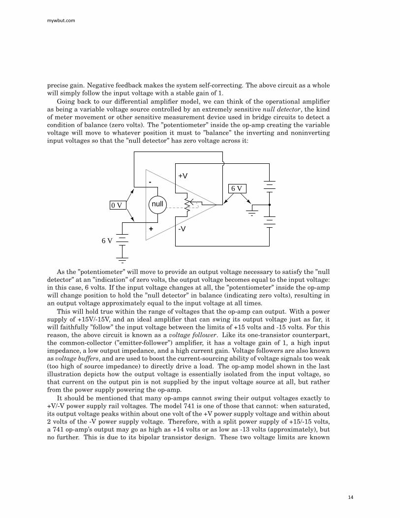
Going back to our differential amplifier model, we can think of the operational amplifieras being a variable voltage source controlled by an extremely sensitive null detector, the kindof meter movement or other sensitive measurement device used in bridge circuits to detect acondition of balance (zero volts). The ”potentiometer” inside the op-amp creating the variablevoltage will move to whatever position it must to ”balance” the inverting and noninvertinginput voltages so that the ”null detector” has zero voltage across it:
null
-
+
+V
-V
6 V
6 V
0 V
As the ”potentiometer” will move to provide an output voltage necessary to satisfy the ”nulldetector” at an ”indication” of zero volts, the output voltage becomes equal to the input voltage:in this case, 6 volts. If the input voltage changes at all, the ”potentiometer” inside the op-ampwill change position to hold the ”null detector” in balance (indicating zero volts), resulting inan output voltage approximately equal to the input voltage at all times.
This will hold true within the range of voltages that the op-amp can output. With a powersupply of +15V/-15V, and an ideal amplifier that can swing its output voltage just as far, itwill faithfully ”follow” the input voltage between the limits of +15 volts and -15 volts. For thisreason, the above circuit is known as a voltage follower. Like its one-transistor counterpart,the common-collector (”emitter-follower”) amplifier, it has a voltage gain of 1, a high inputimpedance, a low output impedance, and a high current gain. Voltage followers are also knownas voltage buffers, and are used to boost the current-sourcing ability of voltage signals too weak(too high of source impedance) to directly drive a load. The op-amp model shown in the lastillustration depicts how the output voltage is essentially isolated from the input voltage, sothat current on the output pin is not supplied by the input voltage source at all, but ratherfrom the power supply powering the op-amp.
It should be mentioned that many op-amps cannot swing their output voltages exactly to+V/-V power supply rail voltages. The model 741 is one of those that cannot: when saturated,its output voltage peaks within about one volt of the +V power supply voltage and within about2 volts of the -V power supply voltage. Therefore, with a split power supply of +15/-15 volts,a 741 op-amp’s output may go as high as +14 volts or as low as -13 volts (approximately), butno further. This is due to its bipolar transistor design. These two voltage limits are known
mywbut.com
14

as the positive saturation voltage and negative saturation voltage, respectively. Other op-amps,such as the model 3130 with field-effect transistors in the final output stage, have the ability toswing their output voltages within millivolts of either power supply rail voltage. Consequently,their positive and negative saturation voltages are practically equal to the supply voltages.
• REVIEW:
• Connecting the output of an op-amp to its inverting (-) input is called negative feedback.This term can be broadly applied to any dynamic system where the output signal is ”fedback” to the input somehow so as to reach a point of equilibrium (balance).
• When the output of an op-amp is directly connected to its inverting (-) input, a voltagefollower will be created. Whatever signal voltage is impressed upon the noninverting (+)input will be seen on the output.
• An op-amp with negative feedback will try to drive its output voltage to whatever levelnecessary so that the differential voltage between the two inputs is practically zero. Thehigher the op-amp differential gain, the closer that differential voltage will be to zero.
• Some op-amps cannot produce an output voltage equal to their supply voltage when sat-urated. The model 741 is one of these. The upper and lower limits of an op-amp’s outputvoltage swing are known as positive saturation voltage and negative saturation voltage,respectively.
8.5 Divided feedback
If we add a voltage divider to the negative feedback wiring so that only a fraction of the outputvoltage is fed back to the inverting input instead of the full amount, the output voltage will bea multiple of the input voltage (please bear in mind that the power supply connections to theop-amp have been omitted once again for simplicity’s sake):
−
+
6 V
The effects of divided negative feedback
R1 R2
1 kΩ 1 kΩ
0 V
6 V
6 V12 V
All voltage figures shown inreference to ground
6 mA 6 mA
mywbut.com
15

If R1 and R2 are both equal and Vin is 6 volts, the op-amp will output whatever voltage isneeded to drop 6 volts across R1 (to make the inverting input voltage equal to 6 volts, as well,keeping the voltage difference between the two inputs equal to zero). With the 2:1 voltagedivider of R1 and R2, this will take 12 volts at the output of the op-amp to accomplish.
Another way of analyzing this circuit is to start by calculating the magnitude and directionof current through R1, knowing the voltage on either side (and therefore, by subtraction, thevoltage across R1), and R1’s resistance. Since the left-hand side of R1 is connected to ground (0volts) and the right-hand side is at a potential of 6 volts (due to the negative feedback holdingthat point equal to Vin), we can see that we have 6 volts across R1. This gives us 6 mA of currentthrough R1 from left to right. Because we know that both inputs of the op-amp have extremelyhigh impedance, we can safely assume they won’t add or subtract any current through thedivider. In other words, we can treat R1 and R2 as being in series with each other: all of theelectrons flowing through R1 must flow through R2. Knowing the current through R2 and theresistance of R2, we can calculate the voltage across R2 (6 volts), and its polarity. Counting upvoltages from ground (0 volts) to the right-hand side of R2, we arrive at 12 volts on the output.
Upon examining the last illustration, one might wonder, ”where does that 6 mA of currentgo?” The last illustration doesn’t show the entire current path, but in reality it comes from thenegative side of the DC power supply, through ground, through R1, through R2, through theoutput pin of the op-amp, and then back to the positive side of the DC power supply through theoutput transistor(s) of the op-amp. Using the null detector/potentiometer model of the op-amp,the current path looks like this:
null
-
+
+V
-V
6 V
R1 R2
1 kΩ 1 kΩ
The 6 volt signal source does not have to supply any current for the circuit: it merelycommands the op-amp to balance voltage between the inverting (-) and noninverting (+) inputpins, and in so doing produce an output voltage that is twice the input due to the dividing effectof the two 1 kΩ resistors.
We can change the voltage gain of this circuit, overall, just by adjusting the values of R1
and R2 (changing the ratio of output voltage that is fed back to the inverting input). Gain canbe calculated by the following formula:
mywbut.com
16

AV = R2
R1+ 1
Note that the voltage gain for this design of amplifier circuit can never be less than 1. Ifwe were to lower R2 to a value of zero ohms, our circuit would be essentially identical to thevoltage follower, with the output directly connected to the inverting input. Since the voltagefollower has a gain of 1, this sets the lower gain limit of the noninverting amplifier. However,the gain can be increased far beyond 1, by increasing R2 in proportion to R1.Also note that the polarity of the output matches that of the input, just as with a voltage
follower. A positive input voltage results in a positive output voltage, and vice versa (withrespect to ground). For this reason, this circuit is referred to as a noninverting amplifier.Just as with the voltage follower, we see that the differential gain of the op-amp is irrele-
vant, so long as its very high. The voltages and currents in this circuit would hardly changeat all if the op-amp’s voltage gain were 250,000 instead of 200,000. This stands as a stark con-trast to single-transistor amplifier circuit designs, where the Beta of the individual transistorgreatly influenced the overall gains of the amplifier. With negative feedback, we have a self-correcting system that amplifies voltage according to the ratios set by the feedback resistors,not the gains internal to the op-amp.Let’s see what happens if we retain negative feedback through a voltage divider, but apply
the input voltage at a different location:
−
+
6 V
R1 R2
1 kΩ 1 kΩ
0 VAll voltage figures shown in
reference to ground
0 V
-6 V
6 mA 6 mA
By grounding the noninverting input, the negative feedback from the output seeks to holdthe inverting input’s voltage at 0 volts, as well. For this reason, the inverting input is referredto in this circuit as a virtual ground, being held at ground potential (0 volts) by the feedback,yet not directly connected to (electrically common with) ground. The input voltage this timeis applied to the left-hand end of the voltage divider (R1 = R2 = 1 kΩ again), so the outputvoltage must swing to -6 volts in order to balance the middle at ground potential (0 volts).Using the same techniques as with the noninverting amplifier, we can analyze this circuit’soperation by determining current magnitudes and directions, starting with R1, and continuingon to determining the output voltage.We can change the overall voltage gain of this circuit, overall, just by adjusting the values
of R1 and R2 (changing the ratio of output voltage that is fed back to the inverting input). Gaincan be calculated by the following formula:
AV = R2
R1
−
Note that this circuit’s voltage gain can be less than 1, depending solely on the ratio of R2
mywbut.com
17

to R1. Also note that the output voltage is always the opposite polarity of the input voltage.A positive input voltage results in a negative output voltage, and vice versa (with respect toground). For this reason, this circuit is referred to as an inverting amplifier. Sometimes, thegain formula contains a negative sign (before the R2/R1 fraction) to reflect this reversal ofpolarities.
These two amplifier circuits we’ve just investigated serve the purpose of multiplying ordividing the magnitude of the input voltage signal. This is exactly how the mathematicaloperations of multiplication and division are typically handled in analog computer circuitry.
• REVIEW:
• By connecting the inverting (-) input of an op-amp directly to the output, we get negativefeedback, which gives us a voltage follower circuit. By connecting that negative feedbackthrough a resistive voltage divider (feeding back a fraction of the output voltage to theinverting input), the output voltage becomes a multiple of the input voltage.
• A negative-feedback op-amp circuit with the input signal going to the noninverting (+)input is called a noninverting amplifier. The output voltage will be the same polarity asthe input. Voltage gain is given by the following equation: AV = (R2/R1) + 1
• A negative-feedback op-amp circuit with the input signal going to the ”bottom” of theresistive voltage divider, with the noninverting (+) input grounded, is called an invertingamplifier. Its output voltage will be the opposite polarity of the input. Voltage gain isgiven by the following equation: AV = -R2/R1
8.6 An analogy for divided feedback
A helpful analogy for understanding divided feedback amplifier circuits is that of a mechanicallever, with relative motion of the lever’s ends representing change in input and output voltages,and the fulcrum (pivot point) representing the location of the ground point, real or virtual.
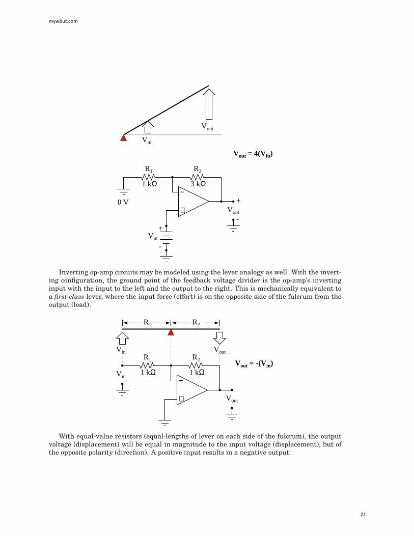
Take for example the following noninverting op-amp circuit. We know from the prior sectionthat the voltage gain of a noninverting amplifier configuration can never be less than unity (1).If we draw a lever diagram next to the amplifier schematic, with the distance between fulcrumand lever ends representative of resistor values, the motion of the lever will signify changes involtage at the input and output terminals of the amplifier:
mywbut.com
18

−
+
R1 R2
1 kΩ 1 kΩ
0 V
Vin
Vin
Vout
R1 R2
Vout = 2(Vin)
Vout
Physicists call this type of lever, with the input force (effort) applied between the fulcrumand output (load), a third-class lever. It is characterized by an output displacement (motion) atleast as large than the input displacement – a ”gain” of at least 1 – and in the same direction.Applying a positive input voltage to this op-amp circuit is analogous to displacing the ”input”point on the lever upward:
mywbut.com
19

−
+
R1 R2
1 kΩ 1 kΩ
0 V
Vin
Vin
Vout
Vout = 2(Vin)
Vout
+
-
+
-
Due to the displacement-amplifying characteristics of the lever, the ”output” point will movetwice as far as the ”input” point, and in the same direction. In the electronic circuit, the outputvoltage will equal twice the input, with the same polarity. Applying a negative input voltage isanalogous to moving the lever downward from its level ”zero” position, resulting in an amplifiedoutput displacement that is also negative:
−
+
R1 R2
1 kΩ 1 kΩ
0 V
Vin
Vin
Vout
Vout = 2(Vin)
Vout
+
-
+
-
mywbut.com
20

If we alter the resistor ratio R2/R1, we change the gain of the op-amp circuit. In lever terms,this means moving the input point in relation to the fulcrum and lever end, which similarlychanges the displacement ”gain” of the machine:
−
+
R1 R2
1 kΩ
0 V
Vin
Vin
Vout
R1 R2
Vout
3 kΩ
Vout = 4(Vin)
Now, any input signal will become amplified by a factor of four instead of by a factor of two:
mywbut.com
21
−
+
R1 R2
1 kΩ
0 V
Vin
Vin
Vout
Vout
3 kΩ
Vout = 4(Vin)
+
-
+
-
Inverting op-amp circuits may be modeled using the lever analogy as well. With the invert-ing configuration, the ground point of the feedback voltage divider is the op-amp’s invertinginput with the input to the left and the output to the right. This is mechanically equivalent toa first-class lever, where the input force (effort) is on the opposite side of the fulcrum from theoutput (load):
−
+
R1 R2
1 kΩ 1 kΩVin
Vout
Vin Vout
Vout = -(Vin)
R1 R2
With equal-value resistors (equal-lengths of lever on each side of the fulcrum), the outputvoltage (displacement) will be equal in magnitude to the input voltage (displacement), but ofthe opposite polarity (direction). A positive input results in a negative output:
mywbut.com
22

−
+
R1 R2
1 kΩ 1 kΩVin
Vout
Vin
Vout
Vout = -(Vin)
+
--
+
Changing the resistor ratio R2/R1 changes the gain of the amplifier circuit, just as changingthe fulcrum position on the lever changes its mechanical displacement ”gain.” Consider thefollowing example, where R2 is made twice as large as R1:
−
+
R1 R2
1 kΩVin
Vout
Vin
Vout
+
--
+2 kΩ
Vout = -2(Vin)
With the inverting amplifier configuration, though, gains of less than 1 are possible, justas with first-class levers. Reversing R2 and R1 values is analogous to moving the fulcrum toits complementary position on the lever: one-third of the way from the output end. There, theoutput displacement will be one-half the input displacement:
mywbut.com
23

−
+
R1 R2
1 kΩVin
Vout
Vin
Vout
+
--
+2 kΩ
Vout = -0.5(Vin)
8.7 Voltage-to-current signal conversion
In instrumentation circuitry, DC signals are often used as analog representations of physicalmeasurements such as temperature, pressure, flow, weight, and motion. Most commonly, DCcurrent signals are used in preference to DC voltage signals, because current signals are ex-actly equal in magnitude throughout the series circuit loop carrying current from the source(measuring device) to the load (indicator, recorder, or controller), whereas voltage signals ina parallel circuit may vary from one end to the other due to resistive wire losses. Further-more, current-sensing instruments typically have low impedances (while voltage-sensing in-struments have high impedances), which gives current-sensing instruments greater electricalnoise immunity.
In order to use current as an analog representation of a physical quantity, we have to havesome way of generating a precise amount of current within the signal circuit. But how dowe generate a precise current signal when we might not know the resistance of the loop?The answer is to use an amplifier designed to hold current to a prescribed value, applyingas much or as little voltage as necessary to the load circuit to maintain that value. Such anamplifier performs the function of a current source. An op-amp with negative feedback is aperfect candidate for such a task:
mywbut.com
24
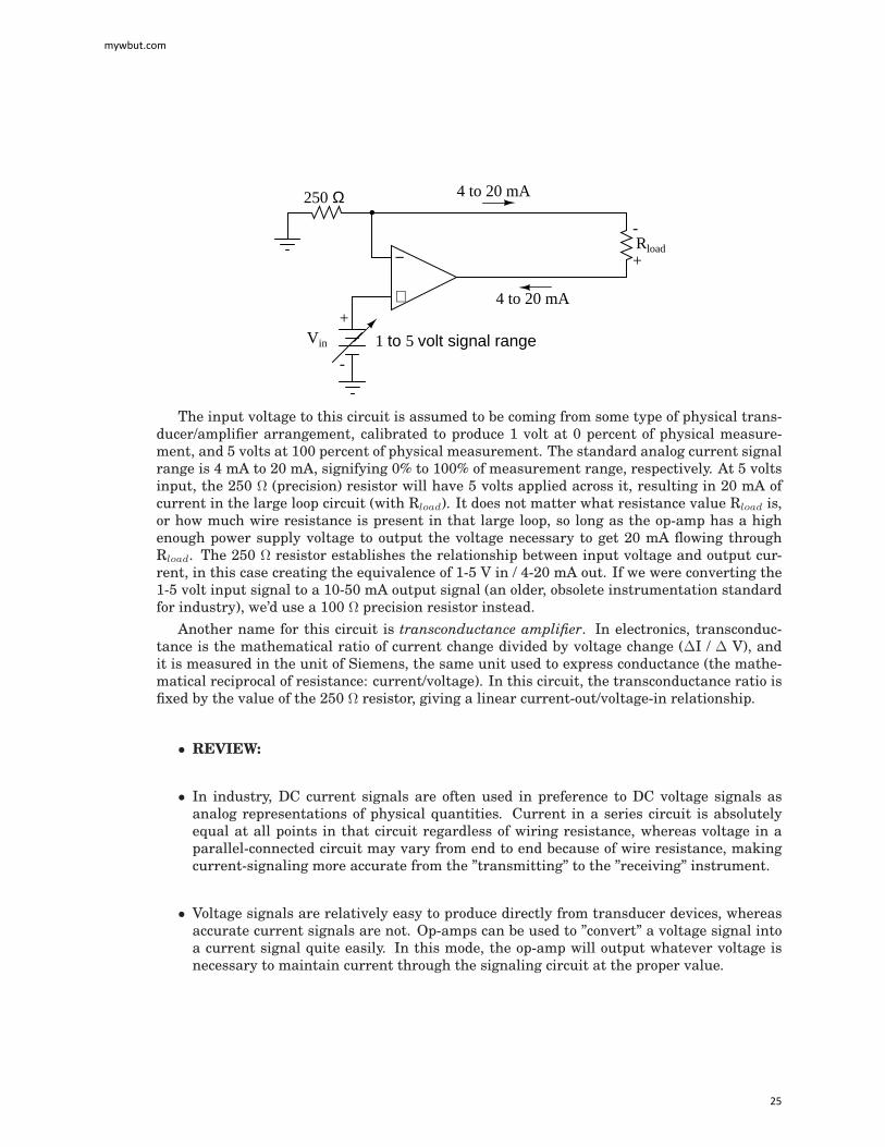
−
+
Vin 1 to 5 volt signal range
Rload
250 Ω 4 to 20 mA
4 to 20 mA
+
-
+
-
The input voltage to this circuit is assumed to be coming from some type of physical trans-ducer/amplifier arrangement, calibrated to produce 1 volt at 0 percent of physical measure-ment, and 5 volts at 100 percent of physical measurement. The standard analog current signalrange is 4 mA to 20 mA, signifying 0% to 100% of measurement range, respectively. At 5 voltsinput, the 250 Ω (precision) resistor will have 5 volts applied across it, resulting in 20 mA ofcurrent in the large loop circuit (with Rload). It does not matter what resistance value Rload is,or how much wire resistance is present in that large loop, so long as the op-amp has a highenough power supply voltage to output the voltage necessary to get 20 mA flowing throughRload. The 250 Ω resistor establishes the relationship between input voltage and output cur-rent, in this case creating the equivalence of 1-5 V in / 4-20 mA out. If we were converting the1-5 volt input signal to a 10-50 mA output signal (an older, obsolete instrumentation standardfor industry), we’d use a 100 Ω precision resistor instead.
Another name for this circuit is transconductance amplifier. In electronics, transconduc-tance is the mathematical ratio of current change divided by voltage change (∆I / ∆ V), andit is measured in the unit of Siemens, the same unit used to express conductance (the mathe-matical reciprocal of resistance: current/voltage). In this circuit, the transconductance ratio isfixed by the value of the 250 Ω resistor, giving a linear current-out/voltage-in relationship.
• REVIEW:
• In industry, DC current signals are often used in preference to DC voltage signals asanalog representations of physical quantities. Current in a series circuit is absolutelyequal at all points in that circuit regardless of wiring resistance, whereas voltage in aparallel-connected circuit may vary from end to end because of wire resistance, makingcurrent-signaling more accurate from the ”transmitting” to the ”receiving” instrument.
• Voltage signals are relatively easy to produce directly from transducer devices, whereasaccurate current signals are not. Op-amps can be used to ”convert” a voltage signal intoa current signal quite easily. In this mode, the op-amp will output whatever voltage isnecessary to maintain current through the signaling circuit at the proper value.
mywbut.com
25
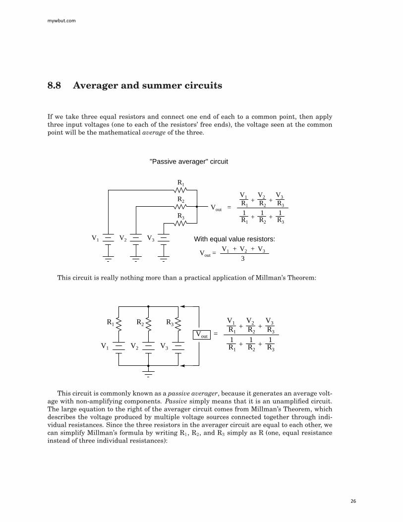
8.8 Averager and summer circuits
If we take three equal resistors and connect one end of each to a common point, then applythree input voltages (one to each of the resistors’ free ends), the voltage seen at the commonpoint will be the mathematical average of the three.
R1
R2
R3
V1 V2 V3
Vout
V1 V2 V3
=+ +R1 R2 R3
R1+ R2
+ R3
1 1 1
"Passive averager" circuit
With equal value resistors:
Vout = V1 V2 V3+ +
3
This circuit is really nothing more than a practical application of Millman’s Theorem:
R1 R2 R3
V1 V2 V3
Vout
V1 V2 V3
=+ +R1 R2 R3
R1+ R2
+ R3
1 1 1
This circuit is commonly known as a passive averager, because it generates an average volt-age with non-amplifying components. Passive simply means that it is an unamplified circuit.The large equation to the right of the averager circuit comes from Millman’s Theorem, whichdescribes the voltage produced by multiple voltage sources connected together through indi-vidual resistances. Since the three resistors in the averager circuit are equal to each other, wecan simplify Millman’s formula by writing R1, R2, and R3 simply as R (one, equal resistanceinstead of three individual resistances):
mywbut.com
26
V1 V2 V3+ +
+ +1 1 1
Vout = V1 V2 V3+ +
3
Vout = R R R
R R R
Vout =
V1 V2 V3+ +R
3R
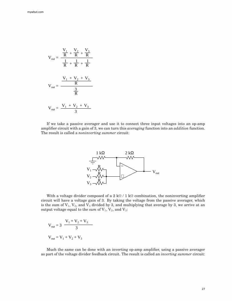
If we take a passive averager and use it to connect three input voltages into an op-ampamplifier circuit with a gain of 3, we can turn this averaging function into an addition function.The result is called a noninverting summer circuit:
−
+
1 kΩ 2 kΩ
R
R
R
V1
V2
V3
Vout
With a voltage divider composed of a 2 kΩ / 1 kΩ combination, the noninverting amplifiercircuit will have a voltage gain of 3. By taking the voltage from the passive averager, whichis the sum of V1, V2, and V3 divided by 3, and multiplying that average by 3, we arrive at anoutput voltage equal to the sum of V1, V2, and V3:
Vout = 3V1 + V2 + V3
3
Vout = V1 + V2 + V3
Much the same can be done with an inverting op-amp amplifier, using a passive averageras part of the voltage divider feedback circuit. The result is called an inverting summer circuit:
mywbut.com
27

−
+
R
R
R
V1
V2
V3Vout
R
I1
I3
I2
I1 + I2 + I30 V
0 V
Now, with the right-hand sides of the three averaging resistors connected to the virtualground point of the op-amp’s inverting input, Millman’s Theorem no longer directly applies asit did before. The voltage at the virtual ground is now held at 0 volts by the op-amp’s negativefeedback, whereas before it was free to float to the average value of V1, V2, and V3. However,with all resistor values equal to each other, the currents through each of the three resistorswill be proportional to their respective input voltages. Since those three currents will add atthe virtual ground node, the algebraic sum of those currents through the feedback resistor willproduce a voltage at Vout equal to V1 + V2 + V3, except with reversed polarity. The reversal inpolarity is what makes this circuit an inverting summer:
Vout = -(V1 + V2 + V3)
Summer (adder) circuits are quite useful in analog computer design, just as multiplier anddivider circuits would be. Again, it is the extremely high differential gain of the op-amp whichallows us to build these useful circuits with a bare minimum of components.
• REVIEW:
• A summer circuit is one that sums, or adds, multiple analog voltage signals together.There are two basic varieties of op-amp summer circuits: noninverting and inverting.
8.9 Building a differential amplifier
An op-amp with no feedback is already a differential amplifier, amplifying the voltage differ-ence between the two inputs. However, its gain cannot be controlled, and it is generally too highto be of any practical use. So far, our application of negative feedback to op-amps has resultingin the practical loss of one of the inputs, the resulting amplifier only good for amplifying a sin-gle voltage signal input. With a little ingenuity, however, we can construct an op-amp circuitmaintaining both voltage inputs, yet with a controlled gain set by external resistors.
mywbut.com
28

−
+
V1
V2
Vout
R R
R R
If all the resistor values are equal, this amplifier will have a differential voltage gain of 1.The analysis of this circuit is essentially the same as that of an inverting amplifier, except thatthe noninverting input (+) of the op-amp is at a voltage equal to a fraction of V2, rather thanbeing connected directly to ground. As would stand to reason, V2 functions as the noninvertinginput and V1 functions as the inverting input of the final amplifier circuit. Therefore:
Vout = V2 - V1
If we wanted to provide a differential gain of anything other than 1, we would have toadjust the resistances in both upper and lower voltage dividers, necessitating multiple resistorchanges and balancing between the two dividers for symmetrical operation. This is not alwayspractical, for obvious reasons.
Another limitation of this amplifier design is the fact that its input impedances are ratherlow compared to that of some other op-amp configurations, most notably the noninverting(single-ended input) amplifier. Each input voltage source has to drive current through a re-sistance, which constitutes far less impedance than the bare input of an op-amp alone. Thesolution to this problem, fortunately, is quite simple. All we need to do is ”buffer” each inputvoltage signal through a voltage follower like this:
−
+
V1
V2
Vout
R R
R R
−
+
−
+
Now the V1 and V2 input lines are connected straight to the inputs of two voltage-followerop-amps, giving very high impedance. The two op-amps on the left now handle the driving ofcurrent through the resistors instead of letting the input voltage sources (whatever they maybe) do it. The increased complexity to our circuit is minimal for a substantial benefit.
mywbut.com
29

8.10 The instrumentation amplifier
As suggested before, it is beneficial to be able to adjust the gain of the amplifier circuit withouthaving to change more than one resistor value, as is necessary with the previous design ofdifferential amplifier. The so-called instrumentation builds on the last version of differentialamplifier to give us that capability:
−
+
V1
V2
Vout
R R
R R
−
+
−
+
R
R
Rgain
3
1
2
4
This intimidating circuit is constructed from a buffered differential amplifier stage withthree new resistors linking the two buffer circuits together. Consider all resistors to be of equalvalue except for Rgain. The negative feedback of the upper-left op-amp causes the voltage atpoint 1 (top of Rgain) to be equal to V1. Likewise, the voltage at point 2 (bottom of Rgain) isheld to a value equal to V2. This establishes a voltage drop across Rgain equal to the voltagedifference between V1 and V2. That voltage drop causes a current through Rgain, and since thefeedback loops of the two input op-amps draw no current, that same amount of current throughRgain must be going through the two ”R” resistors above and below it. This produces a voltagedrop between points 3 and 4 equal to:
V3-4 = (V2 - V1)(1 + 2RRgain
)
The regular differential amplifier on the right-hand side of the circuit then takes this volt-age drop between points 3 and 4, and amplifies it by a gain of 1 (assuming again that all ”R”resistors are of equal value). Though this looks like a cumbersome way to build a differentialamplifier, it has the distinct advantages of possessing extremely high input impedances on theV1 and V2 inputs (because they connect straight into the noninverting inputs of their respec-tive op-amps), and adjustable gain that can be set by a single resistor. Manipulating the aboveformula a bit, we have a general expression for overall voltage gain in the instrumentationamplifier:
2RRgain
)AV = (1 +
Though it may not be obvious by looking at the schematic, we can change the differentialgain of the instrumentation amplifier simply by changing the value of one resistor: Rgain. Yes,we could still change the overall gain by changing the values of some of the other resistors,
mywbut.com
30

but this would necessitate balanced resistor value changes for the circuit to remain symmet-rical. Please note that the lowest gain possible with the above circuit is obtained with Rgain
completely open (infinite resistance), and that gain value is 1.
• REVIEW:
• An instrumentation amplifier is a differential op-amp circuit providing high input impedanceswith ease of gain adjustment through the variation of a single resistor.
8.11 Differentiator and integrator circuits
By introducing electrical reactance into the feedback loops of op-amp amplifier circuits, we cancause the output to respond to changes in the input voltage over time. Drawing their namesfrom their respective calculus functions, the integrator produces a voltage output proportionalto the product (multiplication) of the input voltage and time; and the differentiator (not to beconfused with differential) produces a voltage output proportional to the input voltage’s rate ofchange.Capacitance can be defined as the measure of a capacitor’s opposition to changes in voltage.
The greater the capacitance, the more the opposition. Capacitors oppose voltage change bycreating current in the circuit: that is, they either charge or discharge in response to a changein applied voltage. So, the more capacitance a capacitor has, the greater its charge or dischargecurrent will be for any given rate of voltage change across it. The equation for this is quitesimple:
ChangingDC
voltage
C
i = C dvdt
The dv/dt fraction is a calculus expression representing the rate of voltage change overtime. If the DC supply in the above circuit were steadily increased from a voltage of 15 voltsto a voltage of 16 volts over a time span of 1 hour, the current through the capacitor wouldmost likely be very small, because of the very low rate of voltage change (dv/dt = 1 volt / 3600seconds). However, if we steadily increased the DC supply from 15 volts to 16 volts over ashorter time span of 1 second, the rate of voltage change would be much higher, and thus thecharging current would be much higher (3600 times higher, to be exact). Same amount ofchange in voltage, but vastly different rates of change, resulting in vastly different amounts ofcurrent in the circuit.To put some definite numbers to this formula, if the voltage across a 47 µF capacitor was
changing at a linear rate of 3 volts per second, the current ”through” the capacitor would be(47 µF)(3 V/s) = 141 µA.We can build an op-amp circuit which measures change in voltage by measuring current
through a capacitor, and outputs a voltage proportional to that current:
mywbut.com
31

−
+
Vin
Vout
CR
0 V
0 V
0 V
Differentiator
The right-hand side of the capacitor is held to a voltage of 0 volts, due to the ”virtual ground”effect. Therefore, current ”through” the capacitor is solely due to change in the input voltage.A steady input voltage won’t cause a current through C, but a changing input voltage will.
Capacitor current moves through the feedback resistor, producing a drop across it, whichis the same as the output voltage. A linear, positive rate of input voltage change will resultin a steady negative voltage at the output of the op-amp. Conversely, a linear, negative rateof input voltage change will result in a steady positive voltage at the output of the op-amp.This polarity inversion from input to output is due to the fact that the input signal is beingsent (essentially) to the inverting input of the op-amp, so it acts like the inverting amplifiermentioned previously. The faster the rate of voltage change at the input (either positive ornegative), the greater the voltage at the output.
The formula for determining voltage output for the differentiator is as follows:
Vout = -RCdvin
dt
Applications for this, besides representing the derivative calculus function inside of an ana-log computer, include rate-of-change indicators for process instrumentation. One such rate-of-change signal application might be for monitoring (or controlling) the rate of temperaturechange in a furnace, where too high or too low of a temperature rise rate could be detrimen-tal. The DC voltage produced by the differentiator circuit could be used to drive a comparator,which would signal an alarm or activate a control if the rate of change exceeded a pre-set level.
In process control, the derivative function is used to make control decisions for maintaininga process at setpoint, by monitoring the rate of process change over time and taking action toprevent excessive rates of change, which can lead to an unstable condition. Analog electroniccontrollers use variations of this circuitry to perform the derivative function.
On the other hand, there are applications where we need precisely the opposite function,called integration in calculus. Here, the op-amp circuit would generate an output voltage pro-portional to the magnitude and duration that an input voltage signal has deviated from 0 volts.Stated differently, a constant input signal would generate a certain rate of change in the out-put voltage: differentiation in reverse. To do this, all we have to do is swap the capacitor andresistor in the previous circuit:
mywbut.com
32

−
+
Vin
Vout
CR
0 V
0 V
0 V
Integrator
As before, the negative feedback of the op-amp ensures that the inverting input will be heldat 0 volts (the virtual ground). If the input voltage is exactly 0 volts, there will be no currentthrough the resistor, therefore no charging of the capacitor, and therefore the output voltagewill not change. We cannot guarantee what voltage will be at the output with respect to groundin this condition, but we can say that the output voltage will be constant.
However, if we apply a constant, positive voltage to the input, the op-amp output will fallnegative at a linear rate, in an attempt to produce the changing voltage across the capacitornecessary to maintain the current established by the voltage difference across the resistor.Conversely, a constant, negative voltage at the input results in a linear, rising (positive) voltageat the output. The output voltage rate-of-change will be proportional to the value of the inputvoltage.
The formula for determining voltage output for the integrator is as follows:
dvout
dt= -
Vin
RC
or
Vin
RCdt + c
t
0
Where,c = Output voltage at start time (t=0)
Vout = ∫ -
One application for this device would be to keep a ”running total” of radiation exposure,or dosage, if the input voltage was a proportional signal supplied by an electronic radiationdetector. Nuclear radiation can be just as damaging at low intensities for long periods of timeas it is at high intensities for short periods of time. An integrator circuit would take boththe intensity (input voltage magnitude) and time into account, generating an output voltagerepresenting total radiation dosage.
Another application would be to integrate a signal representing water flow, producing asignal representing total quantity of water that has passed by the flowmeter. This applicationof an integrator is sometimes called a totalizer in the industrial instrumentation trade.
mywbut.com
33
• REVIEW:
• A differentiator circuit produces a constant output voltage for a steadily changing inputvoltage.
• An integrator circuit produces a steadily changing output voltage for a constant inputvoltage.
• Both types of devices are easily constructed, using reactive components (usually capaci-tors rather than inductors) in the feedback part of the circuit.
8.12 Positive feedback
As we’ve seen, negative feedback is an incredibly useful principle when applied to operationalamplifiers. It is what allows us to create all these practical circuits, being able to preciselyset gains, rates, and other significant parameters with just a few changes of resistor values.Negative feedback makes all these circuits stable and self-correcting.
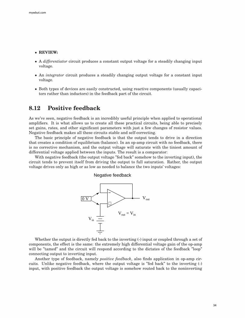
The basic principle of negative feedback is that the output tends to drive in a directionthat creates a condition of equilibrium (balance). In an op-amp circuit with no feedback, thereis no corrective mechanism, and the output voltage will saturate with the tiniest amount ofdifferential voltage applied between the inputs. The result is a comparator:
With negative feedback (the output voltage ”fed back” somehow to the inverting input), thecircuit tends to prevent itself from driving the output to full saturation. Rather, the outputvoltage drives only as high or as low as needed to balance the two inputs’ voltages:
−
+0 V
Vin
Vout
Vout = Vin
Negative feedback
Whether the output is directly fed back to the inverting (-) input or coupled through a set ofcomponents, the effect is the same: the extremely high differential voltage gain of the op-ampwill be ”tamed” and the circuit will respond according to the dictates of the feedback ”loop”connecting output to inverting input.
Another type of feedback, namely positive feedback, also finds application in op-amp cir-cuits. Unlike negative feedback, where the output voltage is ”fed back” to the inverting (-)input, with positive feedback the output voltage is somehow routed back to the noninverting
mywbut.com
34

(+) input. In its simplest form, we could connect a straight piece of wire from output to nonin-verting input and see what happens:
−
+
Vout
Positive feedback
The inverting input remains disconnected from the feedback loop, and is free to receive anexternal voltage. Let’s see what happens if we ground the inverting input:
−
+
Vout
0 V
With the inverting input grounded (maintained at zero volts), the output voltage will bedictated by the magnitude and polarity of the voltage at the noninverting input. If that voltagehappens to be positive, the op-amp will drive its output positive as well, feeding that positivevoltage back to the noninverting input, which will result in full positive output saturation. Onthe other hand, if the voltage on the noninverting input happens to start out negative, the op-amp’s output will drive in the negative direction, feeding back to the noninverting input andresulting in full negative saturation.
What we have here is a circuit whose output is bistable: stable in one of two states (sat-urated positive or saturated negative). Once it has reached one of those saturated states, itwill tend to remain in that state, unchanging. What is necessary to get it to switch states is avoltage placed upon the inverting (-) input of the same polarity, but of a slightly greater mag-nitude. For example, if our circuit is saturated at an output voltage of +12 volts, it will take aninput voltage at the inverting input of at least +12 volts to get the output to change. When itchanges, it will saturate fully negative.
So, an op-amp with positive feedback tends to stay in whatever output state its already in.It ”latches” between one of two states, saturated positive or saturated negative. Technically,this is known as hysteresis.
Hysteresis can be a useful property for a comparator circuit to have. As we’ve seen before,comparators can be used to produce a square wave from any sort of ramping waveform (sinewave, triangle wave, sawtooth wave, etc.) input. If the incoming AC waveform is noise-free(that is, a ”pure” waveform), a simple comparator will work just fine.
mywbut.com
35

−
+
+V
-V
VoutVin
AC inputvoltage
Square waveoutput voltage
DC referencevoltage
A "clean" AC input waveform produces predictabletransition points on the output voltage square wave
However, if there exist any anomalies in the waveform such as harmonics or ”spikes” whichcause the voltage to rise and fall significantly within the timespan of a single cycle, a compara-tor’s output might switch states unexpectedly:
−
+
+V
-V
VoutVin
AC inputvoltage
Square waveoutput voltage
DC referencevoltage
Any time there is a transition through the reference voltage level, no matter how tiny thattransition may be, the output of the comparator will switch states, producing a square wavewith ”glitches.”
If we add a little positive feedback to the comparator circuit, we will introduce hysteresisinto the output. This hysteresis will cause the output to remain in its current state unless theAC input voltage undergoes a major change in magnitude.
mywbut.com
36

−
+
+V
-V
VoutVin
Positive feedbackresistor
What this feedback resistor creates is a dual-reference for the comparator circuit. Thevoltage applied to the noninverting (+) input as a reference which to compare with the incomingAC voltage changes depending on the value of the op-amp’s output voltage. When the op-amp output is saturated positive, the reference voltage at the noninverting input will be morepositive than before. Conversely, when the op-amp output is saturated negative, the referencevoltage at the noninverting input will be more negative than before. The result is easier tounderstand on a graph:
DC reference voltagesupper
centerlower
output voltagesquare wave
AC inputvoltage
When the op-amp output is saturated positive, the upper reference voltage is in effect, andthe output won’t drop to a negative saturation level unless the AC input rises above that upperreference level. Conversely, when the op-amp output is saturated negative, the lower referencevoltage is in effect, and the output won’t rise to a positive saturation level unless the AC inputdrops below that lower reference level. The result is a clean square-wave output again, despitesignificant amounts of distortion in the AC input signal. In order for a ”glitch” to cause thecomparator to switch from one state to another, it would have to be at least as big (tall) as thedifference between the upper and lower reference voltage levels, and at the right point in timeto cross both those levels.
Another application of positive feedback in op-amp circuits is in the construction of oscil-lator circuits. An oscillator is a device that produces an alternating (AC), or at least pulsing,output voltage. Technically, it is known as an astable device: having no stable output state (noequilibrium whatsoever). Oscillators are very useful devices, and they are easily made withjust an op-amp and a few external components.
mywbut.com
37
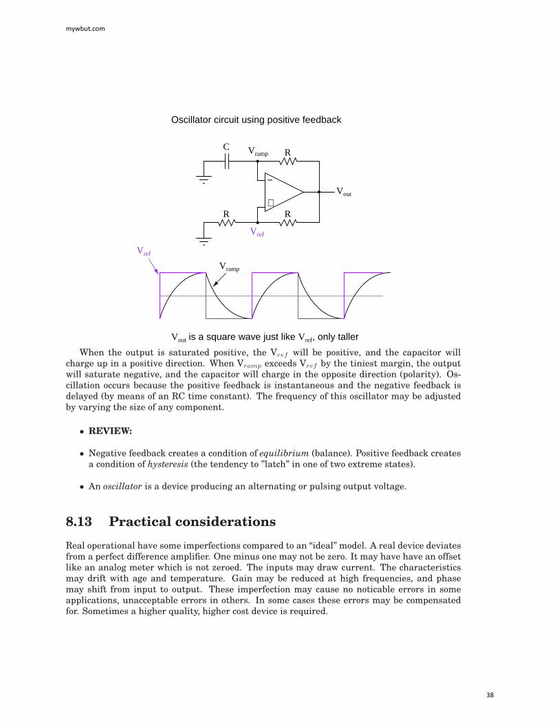
−
+Vout
CR
RR
Vramp
Vref
Vref
Vramp
Vout is a square wave just like Vref, only taller
Oscillator circuit using positive feedback
When the output is saturated positive, the Vref will be positive, and the capacitor willcharge up in a positive direction. When Vramp exceeds Vref by the tiniest margin, the outputwill saturate negative, and the capacitor will charge in the opposite direction (polarity). Os-cillation occurs because the positive feedback is instantaneous and the negative feedback isdelayed (by means of an RC time constant). The frequency of this oscillator may be adjustedby varying the size of any component.
• REVIEW:
• Negative feedback creates a condition of equilibrium (balance). Positive feedback createsa condition of hysteresis (the tendency to ”latch” in one of two extreme states).
• An oscillator is a device producing an alternating or pulsing output voltage.
8.13 Practical considerations
Real operational have some imperfections compared to an “ideal” model. A real device deviatesfrom a perfect difference amplifier. One minus one may not be zero. It may have have an offsetlike an analog meter which is not zeroed. The inputs may draw current. The characteristicsmay drift with age and temperature. Gain may be reduced at high frequencies, and phasemay shift from input to output. These imperfection may cause no noticable errors in someapplications, unacceptable errors in others. In some cases these errors may be compensatedfor. Sometimes a higher quality, higher cost device is required.
mywbut.com
38

8.13.1 Common-mode gain
As stated before, an ideal differential amplifier only amplifies the voltage difference betweenits two inputs. If the two inputs of a differential amplifier were to be shorted together (thusensuring zero potential difference between them), there should be no change in output voltagefor any amount of voltage applied between those two shorted inputs and ground:
−
+Vout
Vcommon-mode
Vout should remain the sameregardless of Vcommon-mode
Voltage that is common between either of the inputs and ground, as ”Vcommon−mode” isin this case, is called common-mode voltage. As we vary this common voltage, the perfectdifferential amplifier’s output voltage should hold absolutely steady (no change in output forany arbitrary change in common-mode input). This translates to a common-mode voltage gainof zero.
AV =Change in Vout
Change in Vin
Change in Vin
0= 0
. . . if change in Vout = 0 . . .
AV = 0
The operational amplifier, being a differential amplifier with high differential gain, wouldideally have zero common-mode gain as well. In real life, however, this is not easily attained.Thus, common-mode voltages will invariably have some effect on the op-amp’s output voltage.
The performance of a real op-amp in this regard is most commonly measured in terms of itsdifferential voltage gain (how much it amplifies the difference between two input voltages) ver-sus its common-mode voltage gain (how much it amplifies a common-mode voltage). The ratioof the former to the latter is called the common-mode rejection ratio, abbreviated as CMRR:
CMRR = Differential AV
Common-mode AV
An ideal op-amp, with zero common-mode gain would have an infinite CMRR. Real op-ampshave high CMRRs, the ubiquitous 741 having something around 70 dB, which works out to a
mywbut.com
39

little over 3,000 in terms of a ratio.Because the common mode rejection ratio in a typical op-amp is so high, common-mode gain
is usually not a great concern in circuits where the op-amp is being used with negative feed-back. If the common-mode input voltage of an amplifier circuit were to suddenly change, thusproducing a corresponding change in the output due to common-mode gain, that change in out-put would be quickly corrected as negative feedback and differential gain (being much greaterthan common-mode gain) worked to bring the system back to equilibrium. Sure enough, achange might be seen at the output, but it would be a lot smaller than what you might expect.A consideration to keep in mind, though, is common-mode gain in differential op-amp cir-
cuits such as instrumentation amplifiers. Outside of the op-amp’s sealed package and ex-tremely high differential gain, we may find common-mode gain introduced by an imbalance ofresistor values. To demonstrate this, we’ll run a SPICE analysis on an instrumentation am-plifier with inputs shorted together (no differential voltage), imposing a common-mode voltageto see what happens. First, we’ll run the analysis showing the output voltage of a perfectlybalanced circuit. We should expect to see no change in output voltage as the common-modevoltage changes:
−
+
V1
Vout
−
+
−
+
Rgain
3
2
R1
R2
2
1
5
6
5
4
7
8
8
7
9
9
0
E1
E2
E3
R3 R4
R5 R6
0
Rjump
(jumperwire)
instrumentation amplifierv1 1 0rin1 1 0 9e12rjump 1 4 1e-12rin2 4 0 9e12e1 3 0 1 2 999ke2 6 0 4 5 999ke3 9 0 8 7 999krload 9 0 10kr1 2 3 10krgain 2 5 10kr2 5 6 10kr3 3 7 10kr4 7 9 10kr5 6 8 10k
mywbut.com
40

r6 8 0 10k.dc v1 0 10 1.print dc v(9).end
v1 v(9)0.000E+00 0.000E+001.000E+00 1.355E-162.000E+00 2.710E-163.000E+00 0.000E+00 As you can see, the output voltage v(9)4.000E+00 5.421E-16 hardly changes at all for a common-mode5.000E+00 0.000E+00 input voltage (v1) that sweeps from 06.000E+00 0.000E+00 to 10 volts.7.000E+00 0.000E+008.000E+00 1.084E-159.000E+00 -1.084E-151.000E+01 0.000E+00
Aside from very small deviations (actually due to quirks of SPICE rather than real behaviorof the circuit), the output remains stable where it should be: at 0 volts, with zero input voltagedifferential. However, let’s introduce a resistor imbalance in the circuit, increasing the value ofR5 from 10,000 Ω to 10,500 Ω, and see what happens (the netlist has been omitted for brevity– the only thing altered is the value of R5):
v1 v(9)0.000E+00 0.000E+001.000E+00 -2.439E-022.000E+00 -4.878E-023.000E+00 -7.317E-02 This time we see a significant variation4.000E+00 -9.756E-02 (from 0 to 0.2439 volts) in output voltage5.000E+00 -1.220E-01 as the common-mode input voltage sweeps6.000E+00 -1.463E-01 from 0 to 10 volts as it did before.7.000E+00 -1.707E-018.000E+00 -1.951E-019.000E+00 -2.195E-011.000E+01 -2.439E-01
Our input voltage differential is still zero volts, yet the output voltage changes significantlyas the common-mode voltage is changed. This is indicative of a common-mode gain, somethingwe’re trying to avoid. More than that, its a common-mode gain of our own making, havingnothing to do with imperfections in the op-amps themselves. With a much-tempered differen-tial gain (actually equal to 3 in this particular circuit) and no negative feedback outside thecircuit, this common-mode gain will go unchecked in an instrument signal application.There is only one way to correct this common-mode gain, and that is to balance all the re-
sistor values. When designing an instrumentation amplifier from discrete components (ratherthan purchasing one in an integrated package), it is wise to provide some means of making
mywbut.com
41

fine adjustments to at least one of the four resistors connected to the final op-amp to be able to”trim away” any such common-mode gain. Providing the means to ”trim” the resistor networkhas additional benefits as well. Suppose that all resistor values are exactly as they shouldbe, but a common-mode gain exists due to an imperfection in one of the op-amps. With theadjustment provision, the resistance could be trimmed to compensate for this unwanted gain.
One quirk of some op-amp models is that of output latch-up, usually caused by the common-mode input voltage exceeding allowable limits. If the common-mode voltage falls outside of themanufacturer’s specified limits, the output may suddenly ”latch” in the high mode (saturate atfull output voltage). In JFET-input operational amplifiers, latch-up may occur if the common-mode input voltage approaches too closely to the negative power supply rail voltage. On theTL082 op-amp, for example, this occurs when the common-mode input voltage comes withinabout 0.7 volts of the negative power supply rail voltage. Such a situation may easily occur ina single-supply circuit, where the negative power supply rail is ground (0 volts), and the inputsignal is free to swing to 0 volts.
Latch-up may also be triggered by the common-mode input voltage exceeding power supplyrail voltages, negative or positive. As a rule, you should never allow either input voltage torise above the positive power supply rail voltage, or sink below the negative power supplyrail voltage, even if the op-amp in question is protected against latch-up (as are the 741 and1458 op-amp models). At the very least, the op-amp’s behavior may become unpredictable. Atworst, the kind of latch-up triggered by input voltages exceeding power supply voltages maybe destructive to the op-amp.
While this problem may seem easy to avoid, its possibility is more likely than you mightthink. Consider the case of an operational amplifier circuit during power-up. If the circuitreceives full input signal voltage before its own power supply has had time enough to chargethe filter capacitors, the common-mode input voltage may easily exceed the power supply railvoltages for a short time. If the op-amp receives signal voltage from a circuit supplied by adifferent power source, and its own power source fails, the signal voltage(s) may exceed thepower supply rail voltages for an indefinite amount of time!
8.13.2 Offset voltage
Another practical concern for op-amp performance is voltage offset. That is, effect of havingthe output voltage something other than zero volts when the two input terminals are shortedtogether. Remember that operational amplifiers are differential amplifiers above all: they’resupposed to amplify the difference in voltage between the two input connections and nothingmore. When that input voltage difference is exactly zero volts, we would (ideally) expect to haveexactly zero volts present on the output. However, in the real world this rarely happens. Evenif the op-amp in question has zero common-mode gain (infinite CMRR), the output voltage maynot be at zero when both inputs are shorted together. This deviation from zero is called offset.
mywbut.com
42

−
+
+15 V
-15 V
Vout = +14.7 V (saturated +)
A perfect op-amp would output exactly zero volts with both its inputs shorted together andgrounded. However, most op-amps off the shelf will drive their outputs to a saturated level,either negative or positive. In the example shown above, the output voltage is saturated at avalue of positive 14.7 volts, just a bit less than +V (+15 volts) due to the positive saturationlimit of this particular op-amp. Because the offset in this op-amp is driving the output to acompletely saturated point, there’s no way of telling how much voltage offset is present at theoutput. If the +V/-V split power supply was of a high enough voltage, who knows, maybe theoutput would be several hundred volts one way or the other due to the effects of offset!
For this reason, offset voltage is usually expressed in terms of the equivalent amount ofinput voltage differential producing this effect. In other words, we imagine that the op-ampis perfect (no offset whatsoever), and a small voltage is being applied in series with one of theinputs to force the output voltage one way or the other away from zero. Being that op-ampdifferential gains are so high, the figure for ”input offset voltage” doesn’t have to be much toaccount for what we see with shorted inputs:
−
+
+15 V
-15 V
Vout = +14.7 V (saturated +)
Input offset voltage(internal to the real op-amp,external to this ideal op-amp)
Offset voltage will tend to introduce slight errors in any op-amp circuit. So how do wecompensate for it? Unlike common-mode gain, there are usually provisions made by the man-ufacturer to trim the offset of a packaged op-amp. Usually, two extra terminals on the op-amppackage are reserved for connecting an external ”trim” potentiometer. These connection pointsare labeled offset null and are used in this general way:
mywbut.com
43

−
+
Potentiometer adjusted so thatVout = 0 volts with inputs shorted together
Vout
+15 V
-15 V
On single op-amps such as the 741 and 3130, the offset null connection points are pins 1and 5 on the 8-pin DIP package. Other models of op-amp may have the offset null connectionslocated on different pins, and/or require a slightly difference configuration of trim potentiome-ter connection. Some op-amps don’t provide offset null pins at all! Consult the manufacturer’sspecifications for details.
8.13.3 Bias current
Inputs on an op-amp have extremely high input impedances. That is, the input currents enter-ing or exiting an op-amp’s two input signal connections are extremely small. For most purposesof op-amp circuit analysis, we treat them as though they don’t exist at all. We analyze the cir-cuit as though there was absolutely zero current entering or exiting the input connections.This idyllic picture, however, is not entirely true. Op-amps, especially those op-amps with
bipolar transistor inputs, have to have some amount of current through their input connec-tions in order for their internal circuits to be properly biased. These currents, logically, arecalled bias currents. Under certain conditions, op-amp bias currents may be problematic. Thefollowing circuit illustrates one of those problem conditions:
−
+Thermocouple Vout
+V
-V
At first glance, we see no apparent problems with this circuit. A thermocouple, generating asmall voltage proportional to temperature (actually, a voltage proportional to the difference intemperature between the measurement junction and the ”reference” junction formed when thealloy thermocouple wires connect with the copper wires leading to the op-amp) drives the op-amp either positive or negative. In other words, this is a kind of comparator circuit, comparingthe temperature between the end thermocouple junction and the reference junction (near theop-amp). The problem is this: the wire loop formed by the thermocouple does not provide a
mywbut.com
44
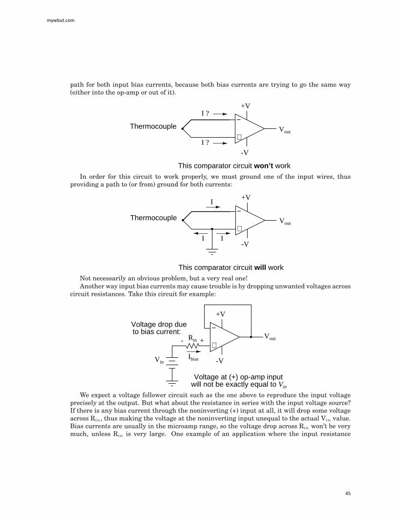
path for both input bias currents, because both bias currents are trying to go the same way(either into the op-amp or out of it).
−
+Thermocouple Vout
+V
-V
I ?
I ?
This comparator circuit won’t workIn order for this circuit to work properly, we must ground one of the input wires, thus
providing a path to (or from) ground for both currents:
−
+Thermocouple Vout
+V
-VI I
I
This comparator circuit will workNot necessarily an obvious problem, but a very real one!Another way input bias currents may cause trouble is by dropping unwanted voltages across
circuit resistances. Take this circuit for example:
−
+Vout
+V
-V
- +Rin
VinIbias
Voltage drop dueto bias current:
Voltage at (+) op-amp inputwill not be exactly equal to Vin
We expect a voltage follower circuit such as the one above to reproduce the input voltageprecisely at the output. But what about the resistance in series with the input voltage source?If there is any bias current through the noninverting (+) input at all, it will drop some voltageacross Rin, thus making the voltage at the noninverting input unequal to the actual Vin value.Bias currents are usually in the microamp range, so the voltage drop across Rin won’t be verymuch, unless Rin is very large. One example of an application where the input resistance
mywbut.com
45
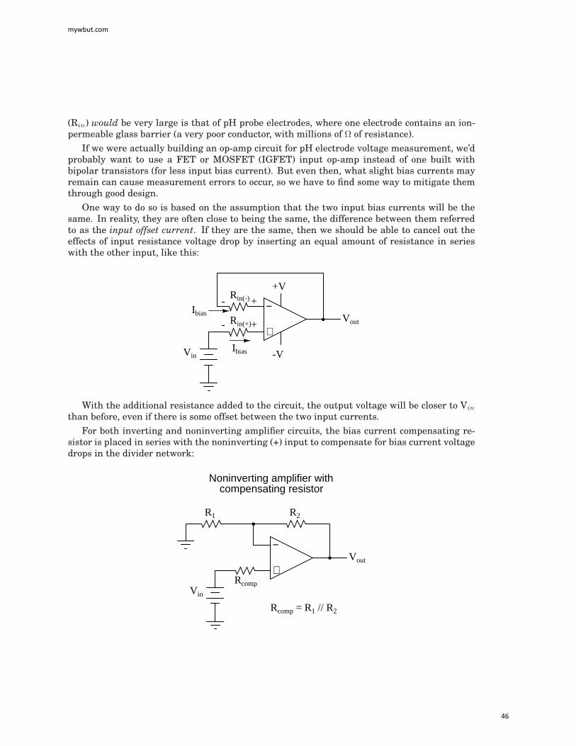
(Rin) would be very large is that of pH probe electrodes, where one electrode contains an ion-permeable glass barrier (a very poor conductor, with millions of Ω of resistance).
If we were actually building an op-amp circuit for pH electrode voltage measurement, we’dprobably want to use a FET or MOSFET (IGFET) input op-amp instead of one built withbipolar transistors (for less input bias current). But even then, what slight bias currents mayremain can cause measurement errors to occur, so we have to find some way to mitigate themthrough good design.
One way to do so is based on the assumption that the two input bias currents will be thesame. In reality, they are often close to being the same, the difference between them referredto as the input offset current. If they are the same, then we should be able to cancel out theeffects of input resistance voltage drop by inserting an equal amount of resistance in serieswith the other input, like this:
−
+Vout
+V
-V
- +
VinIbias
Rin(-)
Rin(+)
Ibias
- +
With the additional resistance added to the circuit, the output voltage will be closer to Vin
than before, even if there is some offset between the two input currents.
For both inverting and noninverting amplifier circuits, the bias current compensating re-sistor is placed in series with the noninverting (+) input to compensate for bias current voltagedrops in the divider network:
−
+Vout
Vin
Rcomp
R1 R2
Noninverting amplifier withcompensating resistor
Rcomp = R1 // R2
mywbut.com
46

−
+Vout
Vin
Rcomp
R1 R2
compensating resistor
Rcomp = R1 // R2
Inverting amplifier with
In either case, the compensating resistor value is determined by calculating the parallelresistance value of R1 and R2. Why is the value equal to the parallel equivalent of R1 and R2?When using the Superposition Theorem to figure how much voltage drop will be produced bythe inverting (-) input’s bias current, we treat the bias current as though it were coming froma current source inside the op-amp and short-circuit all voltage sources (Vin and Vout). Thisgives two parallel paths for bias current (through R1 and through R2, both to ground). Wewant to duplicate the bias current’s effect on the noninverting (+) input, so the resistor valuewe choose to insert in series with that input needs to be equal to R1 in parallel with R2.A related problem, occasionally experienced by students just learning to build operational
amplifier circuits, is caused by a lack of a common ground connection to the power supply. It isimperative to proper op-amp function that some terminal of the DC power supply be commonto the ”ground” connection of the input signal(s). This provides a complete path for the biascurrents, feedback current(s), and for the load (output) current. Take this circuit illustration,for instance, showing a properly grounded power supply:
null
-
+
+V
-V
6 V
R1 R2
1 kΩ 1 kΩ
Here, arrows denote the path of electron flow through the power supply batteries, both forpowering the op-amp’s internal circuitry (the ”potentiometer” inside of it that controls output
mywbut.com
47

voltage), and for powering the feedback loop of resistors R1 and R2. Suppose, however, that theground connection for this ”split” DC power supply were to be removed. The effect of doing thisis profound:
null
-
+
+V
-V
6 V
R1 R2
1 kΩ 1 kΩ
brokenconnection
A power supply ground is essential to circuit operation!
No electrons may flow in or out of the op-amp’s output terminal, because the pathway to thepower supply is a ”dead end.” Thus, no electrons flow through the ground connection to the leftof R1, neither through the feedback loop. This effectively renders the op-amp useless: it canneither sustain current through the feedback loop, nor through a grounded load, since there isno connection from any point of the power supply to ground.
The bias currents are also stopped, because they rely on a path to the power supply and backto the input source through ground. The following diagram shows the bias currents (only), asthey go through the input terminals of the op-amp, through the base terminals of the inputtransistors, and eventually through the power supply terminal(s) and back to ground.
mywbut.com
48
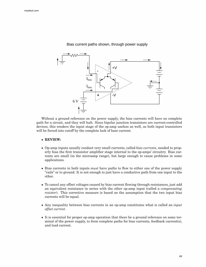
-
+
+V
6 V
Ibias
-V
Ibias
Bias current paths shown, through power supply
Without a ground reference on the power supply, the bias currents will have no completepath for a circuit, and they will halt. Since bipolar junction transistors are current-controlleddevices, this renders the input stage of the op-amp useless as well, as both input transistorswill be forced into cutoff by the complete lack of base current.
• REVIEW:
• Op-amp inputs usually conduct very small currents, called bias currents, needed to prop-erly bias the first transistor amplifier stage internal to the op-amps’ circuitry. Bias cur-rents are small (in the microamp range), but large enough to cause problems in someapplications.
• Bias currents in both inputs must have paths to flow to either one of the power supply”rails” or to ground. It is not enough to just have a conductive path from one input to theother.
• To cancel any offset voltages caused by bias current flowing through resistances, just addan equivalent resistance in series with the other op-amp input (called a compensatingresistor). This corrective measure is based on the assumption that the two input biascurrents will be equal.
• Any inequality between bias currents in an op-amp constitutes what is called an inputoffset current.
• It is essential for proper op-amp operation that there be a ground reference on some ter-minal of the power supply, to form complete paths for bias currents, feedback current(s),and load current.
mywbut.com
49
8.13.4 Drift
Being semiconductor devices, op-amps are subject to slight changes in behavior with changesin operating temperature. Any changes in op-amp performance with temperature fall underthe category of op-amp drift. Drift parameters can be specified for bias currents, offset voltage,and the like. Consult the manufacturer’s data sheet for specifics on any particular op-amp.To minimize op-amp drift, we can select an op-amp made to have minimum drift, and/or we
can do our best to keep the operating temperature as stable as possible. The latter action mayinvolve providing some form of temperature control for the inside of the equipment housingthe op-amp(s). This is not as strange as it may first seem. Laboratory-standard precisionvoltage reference generators, for example, are sometimes known to employ ”ovens” for keepingtheir sensitive components (such as zener diodes) at constant temperatures. If extremely highaccuracy is desired over the usual factors of cost and flexibility, this may be an option worthlooking at.
• REVIEW:
• Op-amps, being semiconductor devices, are susceptible to variations in temperature. Anyvariations in amplifier performance resulting from changes in temperature is known asdrift. Drift is best minimized with environmental temperature control.
8.13.5 Frequency response
With their incredibly high differential voltage gains, op-amps are prime candidates for a phe-nomenon known as feedback oscillation. You’ve probably heard the equivalent audio effectwhen the volume (gain) on a public-address or other microphone amplifier system is turnedtoo high: that high pitched squeal resulting from the sound waveform ”feeding back” throughthe microphone to be amplified again. An op-amp circuit can manifest this same effect, withthe feedback happening electrically rather than audibly.A case example of this is seen in the 3130 op-amp, if it is connected as a voltage follower
with the bare minimum of wiring connections (the two inputs, output, and the power supplyconnections). The output of this op-amp will self-oscillate due to its high gain, no matterwhat the input voltage. To combat this, a small compensation capacitor must be connectedto two specially-provided terminals on the op-amp. The capacitor provides a high-impedancepath for negative feedback to occur within the op-amp’s circuitry, thus decreasing the AC gainand inhibiting unwanted oscillations. If the op-amp is being used to amplify high-frequencysignals, this compensation capacitor may not be needed, but it is absolutely essential for DC orlow-frequency AC signal operation.Some op-amps, such as the model 741, have a compensation capacitor built in to minimize
the need for external components. This improved simplicity is not without a cost: due to thatcapacitor’s presence inside the op-amp, the negative feedback tends to get stronger as theoperating frequency increases (that capacitor’s reactance decreases with higher frequencies).As a result, the op-amp’s differential voltage gain decreases as frequency goes up: it becomesa less effective amplifier at higher frequencies.Op-amp manufacturers will publish the frequency response curves for their products. Since
a sufficiently high differential gain is absolutely essential to good feedback operation in op-amp
mywbut.com
50

circuits, the gain/frequency response of an op-amp effectively limits its ”bandwidth” of opera-tion. The circuit designer must take this into account if good performance is to be maintainedover the required range of signal frequencies.
• REVIEW:
• Due to capacitances within op-amps, their differential voltage gain tends to decrease asthe input frequency increases. Frequency response curves for op-amps are available fromthe manufacturer.
8.13.6 Input to output phase shift
In order to illustrate the phase shift from input to output of an operational amplifier (op-amp),the OPA227 was tested in our lab. The OPA227 was constructed in a typical non-invertingconfiguration (Figure 8.1).
Figure 8.1: OPA227 Non-inverting stage
The circuit configuration calls for a signal gain of ∼=34 V/V or ∼=50 dB. The input excitationat Vsrc was set to 10 mVp, and three frequencies of interest: 2.2 kHz, 22 kHz, and 220 MHz.The OPA227’s open loop gain and phase curve vs. frequency is shown in Figure 8.2.To help predict the closed loop phase shift from input to output, we can use the open loop
gain and phase curve. Since the circuit configuration calls for a closed loop gain, or 1/β, of∼=50 dB, the closed loop gain curve intersects the open loop gain curve at approximately 22kHz. After this intersection, the closed loop gain curve rolls off at the typical 20 dB/decade forvoltage feedback amplifiers, and follows the open loop gain curve.What is actually at work here is the negative feedback from the closed loop modifies the
open loop response. Closing the loop with negative feedback establishes a closed loop pole at22 kHz. Much like the dominant pole in the open loop phase curve, we will expect phase shiftin the closed loop response. How much phase shift will we see?Since the new pole is now at 22 kHz, this is also the -3 dB point as the pole starts to roll off
the closed loop again at 20 dB per decade as stated earlier. As with any pole in basic controltheory, phase shift starts to occur one decade in frequency before the pole, and ends at 90o ofphase shift one decade in frequency after the pole. So what does this predict for the closed loopresponse in our circuit?
mywbut.com
51

Figure 8.2: AV and Φ vs. Frequency plot
This will predict phase shift starting at 2.2 kHz, with 45o of phase shift at the -3 dB point of22 kHz, and finally ending with 90o of phase shift at 220 kHz. The three Figures shown beloware oscilloscope captures at the frequencies of interest for our OPA227 circuit. Figure 8.3 isset for 2.2 kHz, and no noticeable phase shift is present. Figure 8.4 is set for 220 kHz, and∼=45o of phase shift is recorded. Finally, Figure 8.5 is set for 220 MHz, and the expected ∼=90o
of phase shift is recorded. The scope plots were captured using a LeCroy 44x Wavesurfer. Thefinal scope plot used a x1 probe with the trigger set to HF reject.
Figure 8.3: OPA227 Av=50dB @ 2.2 kHz
mywbut.com
52

Figure 8.4: OPA227 Av=50dB @ 22 kHz
Figure 8.5: OPA227 Av=50dB @ 220 kHz
mywbut.com
53

8.14 Operational amplifier models
While mention of operational amplifiers typically provokes visions of semiconductor devicesbuilt as integrated circuits on a miniature silicon chip, the first op-amps were actually vacuumtube circuits. The first commercial, general purpose operational amplifier was manufacturedby the George A. Philbrick Researches, Incorporated, in 1952. Designated the K2-W, it wasbuilt around two twin-triode tubes mounted in an assembly with an octal (8-pin) socket for easyinstallation and servicing in electronic equipment chassis of that era. The assembly lookedsomething like this:
The Philbrick Researchesop-amp, model K2-W
GAP/RMODELK2-W
4 inchesapprox.
The schematic diagram shows the two tubes, along with ten resistors and two capacitors, afairly simple circuit design even by 1952 standards:
12AX7
+300 V
220 kΩ
220 kΩ
-300 V
Inverting (-)input
Noninverting (+)input
1 MΩ
2 2 MΩ
510 kΩ
120 kΩ 4 7 MΩ221 kΩ
9 1 kΩ
12AX7
680 kΩ
7 5 pF
500 pF
NE-68
Output
The Philbrick Researches op-amp, model K2-W
In case you’re unfamiliar with the operation of vacuum tubes, they operate similarly to N-
mywbut.com
54

channel depletion-type IGFET transistors: that is, they conduct more current when the controlgrid (the dashed line) is made more positive with respect to the cathode (the bent line near thebottom of the tube symbol), and conduct less current when the control grid is made less positive(or more negative) than the cathode. The twin triode tube on the left functions as a differentialpair, converting the differential inputs (inverting and noninverting input voltage signals) intoa single, amplified voltage signal which is then fed to the control grid of the left triode ofthe second triode pair through a voltage divider (1 MΩ −− 2.2 MΩ). That triode amplifiesand inverts the output of the differential pair for a larger voltage gain, then the amplifiedsignal is coupled to the second triode of the same dual-triode tube in a noninverting amplifierconfiguration for a larger current gain. The two neon ”glow tubes” act as voltage regulators,similar to the behavior of semiconductor zener diodes, to provide a bias voltage in the couplingbetween the two single-ended amplifier triodes.With a dual-supply voltage of +300/-300 volts, this op-amp could only swing its output +/-
50 volts, which is very poor by today’s standards. It had an open-loop voltage gain of 15,000to 20,000, a slew rate of +/- 12 volts/µsecond, a maximum output current of 1 mA, a quiescentpower consumption of over 3 watts (not including power for the tubes’ filaments!), and costabout $24 in 1952 dollars. Better performance could have been attained using a more sophis-ticated circuit design, but only at the expense of greater power consumption, greater cost, anddecreased reliability.With the advent of solid-state transistors, op-amps with far less quiescent power consump-
tion and increased reliability became feasible, but many of the other performance parametersremained about the same. Take for instance Philbrick’s model P55A, a general-purpose solid-state op-amp circa 1966. The P55A sported an open-loop gain of 40,000, a slew rate of 1.5volt/µsecond and an output swing of +/- 11 volts (at a power supply voltage of +/- 15 volts),a maximum output current of 2.2 mA, and a cost of $49 (or about $21 for the ”utility grade”version). The P55A, as well as other op-amps in Philbrick’s lineup of the time, was of discrete-component construction, its constituent transistors, resistors, and capacitors housed in a solid”brick” resembling a large integrated circuit package.It isn’t very difficult to build a crude operational amplifier using discrete components. A
schematic of one such circuit is shown in Figure 8.6.While its performance is rather dismal by modern standards, it demonstrates that com-
plexity is not necessary to create a minimally functional op-amp. Transistors Q3 and Q4 formthe heart of another differential pair circuit, the semiconductor equivalent of the first triodetube in the K2-W schematic. As it was in the vacuum tube circuit, the purpose of a differen-tial pair is to amplify and convert a differential voltage between the two input terminals to asingle-ended output voltage.With the advent of integrated-circuit (IC) technology, op-amp designs experienced a dra-
matic increase in performance, reliability, density, and economy. Between the years of 1964and 1968, the Fairchild corporation introduced three models of IC op-amps: the 702, 709, andthe still-popular 741. While the 741 is now considered outdated in terms of performance, it isstill a favorite among hobbyists for its simplicity and fault tolerance (short-circuit protectionon the output, for instance). Personal experience abusing many 741 op-amps has led me to theconclusion that it is a hard chip to kill . . .The internal schematic diagram for a model 741 op-amp is shown in Figure 8.7.By integrated circuit standards, the 741 is a very simple device: an example of small-
scale integration, or SSI technology. It would be no small matter to build this circuit using
mywbut.com
55

Q1 Q2
Q3 Q4
Q5 Q6
-V
+V
(-) inputinput (+)
Output
A simple operationalamplifier made fromdiscrete components
Figure 8.6: A simple operational amplifier made from discrete components.
Q3 Q4
Q1 Q2
Q5 Q6
R1 R2R3 R4
Q7
Q10
Q8 Q9 Q12
Q11
R5(+) input
(-) input
Q13
offset nulloffset null
+V
-V
Q23
Q16
R9 R8
C1
Q17
Q24
Q22
Q19
Q18
R10
Q15
Q14
R6
OutputR7
Q21
Q20
R11
Internal schematic of a model 741 operational amplifier
Figure 8.7: Schematic diagram of a model 741 op-amp.
mywbut.com
56

discrete components, so you can see the advantages of even the most primitive integratedcircuit technology over discrete components where high parts counts are involved.For the hobbyist, student, or engineer desiring greater performance, there are literally hun-
dreds of op-amp models to choose from. Many sell for less than a dollar apiece, even retail!Special-purpose instrumentation and radio-frequency (RF) op-amps may be quite a bit moreexpensive. In this section I will showcase several popular and affordable op-amps, comparingand contrasting their performance specifications. The venerable 741 is included as a ”bench-mark” for comparison, although it is, as I said before, considered an obsolete design.
Table 8.1: Widely used operational amplifiersModel Devices/
package
Power
supply
Bandwidth Bias
current
Slew
rate
Output
current
number (count) (V) (MHz) (nA) (V/µS) (mA)
TL082 2 12 / 36 4 8 13 17LM301A 1 10 / 36 1 250 0.5 25LM318 1 10 / 40 15 500 70 20LM324 4 3 / 32 1 45 0.25 20LF353 2 12 / 36 4 8 13 20LF356 1 10 / 36 5 8 12 25LF411 1 10 / 36 4 20 15 25741C 1 10 / 36 1 500 0.5 25LM833 2 10 / 36 15 1050 7 40LM1458 2 6 / 36 1 800 10 45CA3130 1 5 / 16 15 0.05 10 20
Listed in Table 8.1 are but a few of the low-cost operational amplifier models widely avail-able from electronics suppliers. Most of them are available through retail supply stores such asRadio Shack. All are under $1.00 cost direct from the manufacturer (year 2001 prices). As youcan see, there is substantial variation in performance between some of these units. Take forinstance the parameter of input bias current: the CA3130 wins the prize for lowest, at 0.05 nA(or 50 pA), and the LM833 has the highest at slightly over 1 µA. The model CA3130 achievesits incredibly low bias current through the use of MOSFET transistors in its input stage. Onemanufacturer advertises the 3130’s input impedance as 1.5 tera-ohms, or 1.5 x 10¹² Ω! Otherop-amps shown here with low bias current figures use JFET input transistors, while the highbias current models use bipolar input transistors.While the 741 is specified in many electronic project schematics and showcased in many
textbooks, its performance has long been surpassed by other designs in every measure. Evensome designs originally based on the 741 have been improved over the years to far surpassoriginal design specifications. One such example is the model 1458, two op-amps in an 8-pinDIP package, which at one time had the exact same performance specifications as the single741. In its latest incarnation it boasts a wider power supply voltage range, a slew rate 50times as great, and almost twice the output current capability of a 741, while still retainingthe output short-circuit protection feature of the 741. Op-amps with JFET and MOSFET inputtransistors far exceed the 741’s performance in terms of bias current, and generally manage tobeat the 741 in terms of bandwidth and slew rate as well.
mywbut.com
57

My own personal recommendations for op-amps are as such: when low bias current is apriority (such as in low-speed integrator circuits), choose the 3130. For general-purpose DCamplifier work, the 1458 offers good performance (and you get two op-amps in the space ofone package). For an upgrade in performance, choose the model 353, as it is a pin-compatiblereplacement for the 1458. The 353 is designed with JFET input circuitry for very low biascurrent, and has a bandwidth 4 times are great as the 1458, although its output current limitis lower (but still short-circuit protected). It may be more difficult to find on the shelf of yourlocal electronics supply house, but it is just as reasonably priced as the 1458.If low power supply voltage is a requirement, I recommend the model 324, as it functions
on as low as 3 volts DC. Its input bias current requirements are also low, and it provides fourop-amps in a single 14-pin chip. Its major weakness is speed, limited to 1 MHz bandwidth andan output slew rate of only 0.25 volts per µs. For high-frequency AC amplifier circuits, the 318is a very good ”general purpose” model.Special-purpose op-amps are available for modest cost which provide better performance
specifications. Many of these are tailored for a specific type of performance advantage, such asmaximum bandwidth or minimum bias current. Take for instance the op-amps, both designedfor high bandwidth in Table 8.2.
Table 8.2: High bandwidth operational amplifiersModel Devices/
package
Power
supply
Bandwidth Bias
current
Slew
rate
Output
current
number (count) (V) (MHz) (nA) (V/µS) (mA)
CLC404 1 10 / 14 232 44,000 2600 70CLC425 1 5 / 14 1900 40,000 350 90
The CLC404 lists at $21.80 (almost as much as George Philbrick’s first commercial op-amp, albeit without correction for inflation), while the CLC425 is quite a bit less expensive at$3.23 per unit. In both cases high speed is achieved at the expense of high bias currents andrestrictive power supply voltage ranges. Some op-amps, designed for high power output arelisted in Table 8.3.
Table 8.3: High current operational amplifiersModel Devices/
package
Power
supply
Bandwidth Bias
current
Slew
rate
Output
current
number (count) (V) (MHz) (nA) (V/µS) (mA)
LM12CL 1 15 / 80 0.7 1000 9 13,000LM7171 1 5.5 / 36 200 12,000 4100 100
Yes, the LM12CL actually has an output current rating of 13 amps (13,000 milliamps)!It lists at $14.40, which is not a lot of money, considering the raw power of the device. TheLM7171, on the other hand, trades high current output ability for fast voltage output ability(a high slew rate). It lists at $1.19, about as low as some ”general purpose” op-amps.Amplifier packages may also be purchased as complete application circuits as opposed to
bare operational amplifiers. The Burr-Brown and Analog Devices corporations, for example,
mywbut.com
58
both long known for their precision amplifier product lines, offer instrumentation amplifiersin pre-designed packages as well as other specialized amplifier devices. In designs where highprecision and repeatability after repair is important, it might be advantageous for the circuitdesigner to choose such a pre-engineered amplifier ”block” rather than build the circuit fromindividual op-amps. Of course, these units typically cost quite a bit more than individual op-amps.
8.15 Data
Parametrical data for all semiconductor op-amp models except the CA3130 comes from Na-tional Semiconductor’s online resources, available at this website: (http://www.national.com).Data for the CA3130 comes from Harris Semiconductor’s CA3130/CA3130A datasheet (filenumber 817.4).
mywbut.com
59

mywbut.com
60