operational amplifiers (op-amps) · an operational amplifier, or op-amp, ... the difference voltage...
TRANSCRIPT

Module: Electronics II Module Number: 650321 Electronic Devices and Circuit Theory, 9th ed., Boylestad and Nashelsky
Philadelphia University Faculty of Engineering
Communication and Electronics Engineering
Amplifier Circuits-III
Operational Amplifiers (Op-Amps):
An operational amplifier, or op-amp, is a very high gain differential amplifier with high input impedance and low output impedance.
Typical uses of the operational amplifier are to provide voltage amplitude changes (amplitude and polarity), oscillators, filter circuits, and many types of instrumentation circuits.
An op-amp contains a number of differential amplifier stages to achieve a very high voltage gain.
- Symbol and Terminals:
The following Figure shows a basic op-amp with two inputs and one output as would result using a differential amplifier input stage. Each input results in either the same or an opposite polarity (or phase) output, depending on whether the signal is applied to the plus (+) or the minus (-) input. To illustrate what an op-amp is, let's consider its ideal characteristics. A practical op-amp, of course, falls short of these ideal standards, but it is much easier to understand and analyze the device from an ideal point of view. These two considerations are clearly shown in the Figure Below.
Firstly, the ideal op-amp has - infinite voltage gain, - infinite bandwidth, - it has an infinite input impedance (open) so that it does not load the driving
source, - a zero output impedance.
Lecturer: Dr. Omar Daoud Part III 1

Module: Electronics II Module Number: 650321 Electronic Devices and Circuit Theory, 9th ed., Boylestad and Nashelsky
The input voltage, Vin appears between the two input terminals, and the output voltage is AvVin as indicated by the internal voltage source symbol.
Secondly, characteristics of a practical op-amp are:
- very high voltage gain, - very high input impedance, - low output impedance, and - wide bandwidth.
- Internal Block Diagram:
A typical op-amp is made up of three types of amplifier circuit: a differential amplifier, a voltage amplifier, and a push-pull amplifier, as shown in the Figure below.
A differential amplifier is the input stage for the op-amp; it provides amplification of the difference voltage between the two inputs. The second stage is usually a class A amplifier that provides additional gain. Some op-amps may have more than one voltage amplifier stage. A push-pull class B amplifier is typically used for the output stage.
Lecturer: Dr. Omar Daoud Part III 2

Module: Electronics II Module Number: 650321 Electronic Devices and Circuit Theory, 9th ed., Boylestad and Nashelsky
The Differential Amplifier Input Stage The term differential comes from the amplifier's ability to amplify the difference of two input signals applied to its inputs . Only the difference in the two signals is amplified; if there is no difference, the output is zero .
A basic differential amplifier circuit and its symbol are shown in the Figure. The transistors (Q1 and Q2) and the collector resistors (Rc1 and Rc2) are carefully matched to have identical characteristics. Notice that the two transistors share a single emitter resistor, RE.
The Differential Amplifier Operation:
- Assume both bases are connected to ground, - The emitter voltage will be -0.7 V because the voltage drops across both base-
emitter junctions are equa1. - The emitter currents are equal (IE1 = IE2) and each is one-half of the current
through RE. - The collector currents are both equal and are approximately equal to the emitter
currents. Because the collector currents are the same, the collector voltages are also the same, which reflects the zero difference in the input voltages (both bases are at 0V.
- If the base of Q1 is disconnected from ground and connected to a small positive voltage,
- Ql will conduct more current because the positive voltage on its base causes the emitter voltage to increase slightly.
- Although the emitter voltage is a little higher, the total current through RE is nearly the same as before.
- The emitter current is now divided so that more of it is in Ql and less in Q2.
- As a result, the collector voltage of Q1 will decrease and the collector voltage of Q2 will increase, reflecting the difference in the input voltages (one is 0 V and the other at a small positive value).
Lecturer: Dr. Omar Daoud Part III 3

Module: Electronics II Module Number: 650321 Electronic Devices and Circuit Theory, 9th ed., Boylestad and Nashelsky
- If the base of Ql is placed back at ground and a small positive voltage is connected to the base of Q2,
- Q2 will conduct more current, - Ql will conduct less, - The emitter current is now divided so that more of it is in Q2 and less in
Q1, - As a result, the collector voltage of Q1 will increase and the collector
voltage of Q2 will decrease. - The differential amplifier exhibits three modes of operation based on the type of
input signals. These modes are single-ended, differential, and common. Since the differential amplifier is the input stage of the op-amp, the op-amp exhibits the same modes.
Op-Amp Input Modes and Parameters 1) Input Signal Modes Single-Ended Mode: one input is grounded and a signal voltage is applied
only to the other input. - In the case where the signal voltage is applied to the inverting input, an
inverted, amplified signal voltage appears at the output. - In the case where the signal is applied to the noninverting input with
the inverting input grounded, a non inverted, amplified signal voltage appears at the output.
Differential Input Mode: Two opposite-polarity (out-of-phase) signals are
applied to the inputs. This type of operation is also referred to as double-ended. The amplified difference between the two inputs appears on the output.
Lecturer: Dr. Omar Daoud Part III 4
Module: Electronics II Module Number: 650321 Electronic Devices and Circuit Theory, 9th ed., Boylestad and Nashelsky
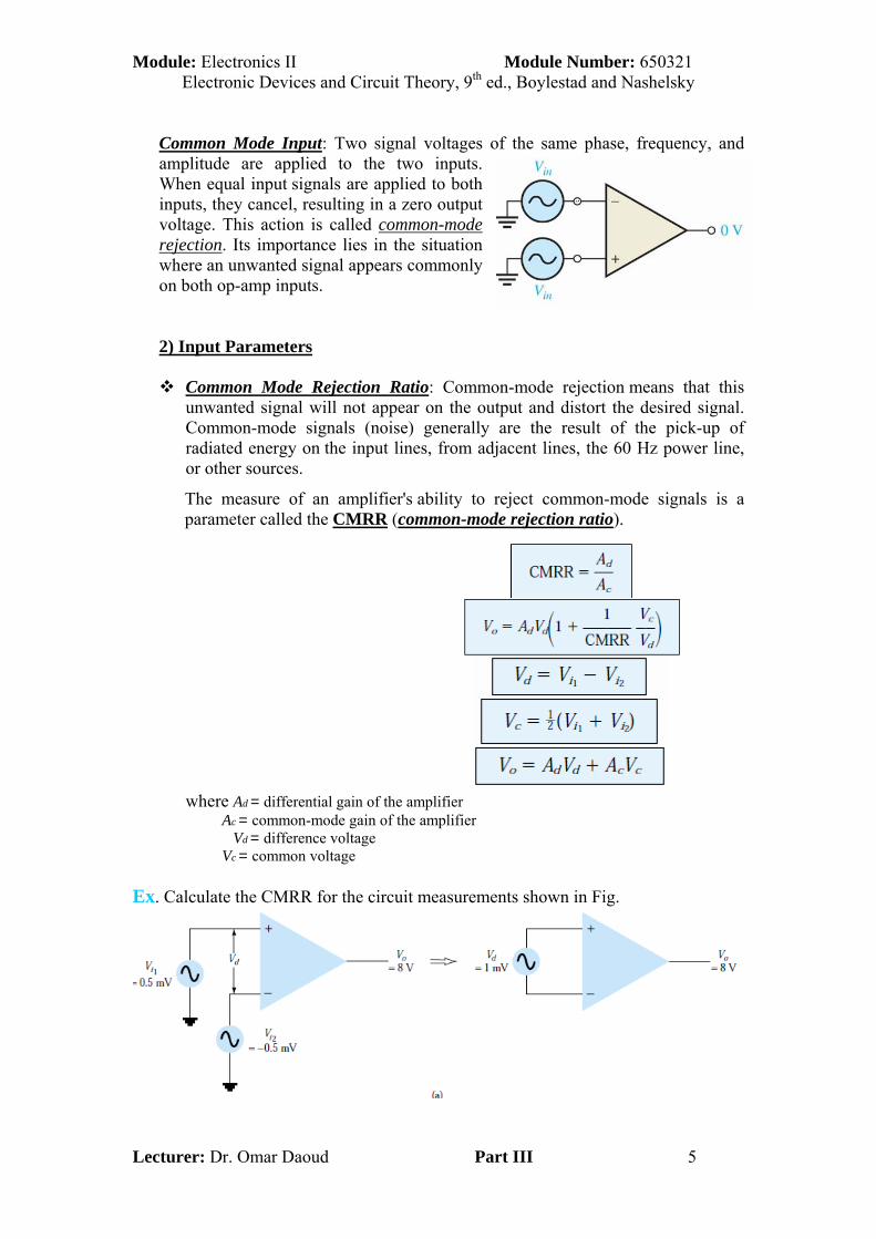
Common Mode Input: Two signal voltages of the same phase, frequency, and amplitude are applied to the two inputs. When equal input signals are applied to both inputs, they cancel, resulting in a zero output voltage. This action is called common-mode rejection. Its importance lies in the situation where an unwanted signal appears commonly on both op-amp inputs. 2) Input Parameters
Common Mode Rejection Ratio: Common-mode rejection means that this
unwanted signal will not appear on the output and distort the desired signal. Common-mode signals (noise) generally are the result of the pick-up of radiated energy on the input lines, from adjacent lines, the 60 Hz power line, or other sources.
The measure of an amplifier's ability to reject common-mode signals is a parameter called the CMRR (common-mode rejection ratio).
where Ad = differential gain of the amplifier Ac = common-mode gain of the amplifier Vd = difference voltage Vc = common voltage Ex. Calculate the CMRR for the circuit measurements shown in Fig.
Lecturer: Dr. Omar Daoud Part III 5
Module: Electronics II Module Number: 650321 Electronic Devices and Circuit Theory, 9th ed., Boylestad and Nashelsky
Solution:
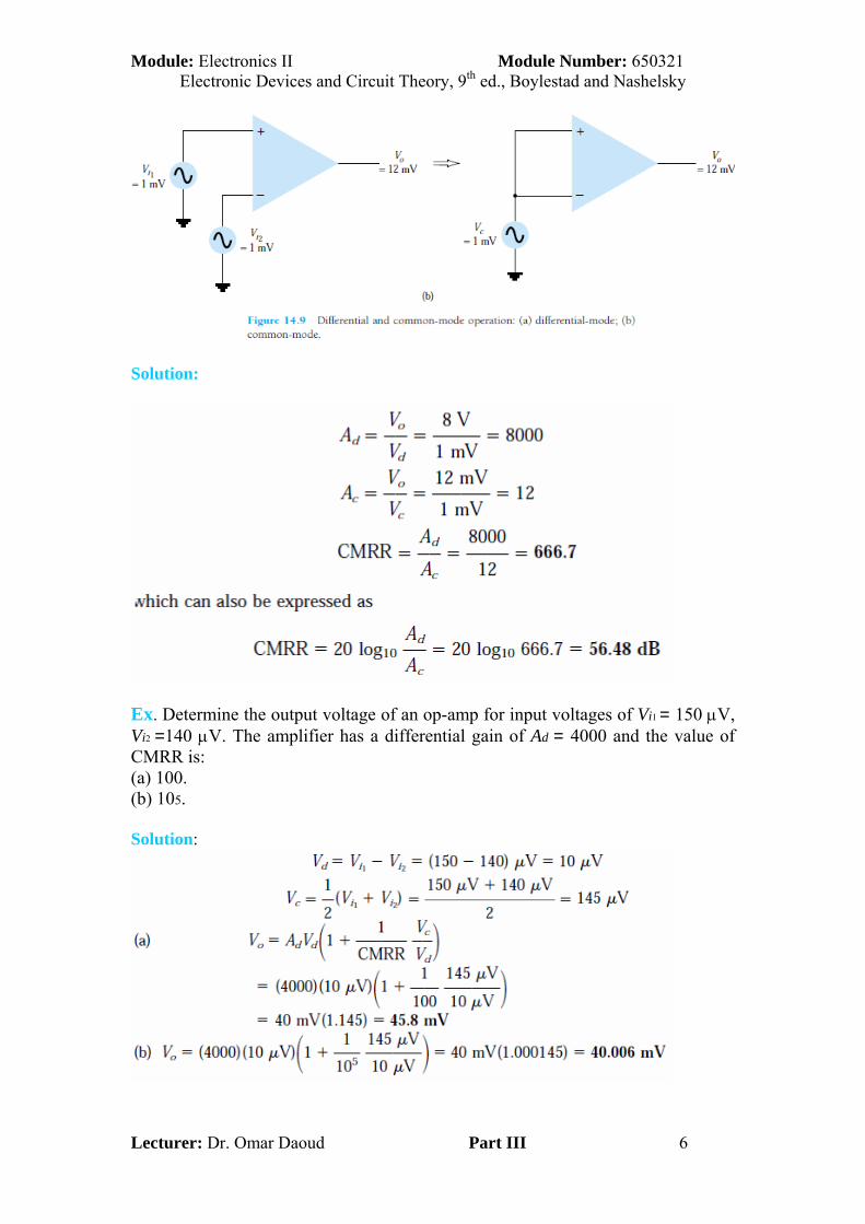
Ex. Determine the output voltage of an op-amp for input voltages of Vi1 = 150 V, Vi2 =140 V. The amplifier has a differential gain of Ad = 4000 and the value of CMRR is: (a) 100. (b) 105. Solution:
Lecturer: Dr. Omar Daoud Part III 6

Module: Electronics II Module Number: 650321 Electronic Devices and Circuit Theory, 9th ed., Boylestad and Nashelsky
Common mode Input voltage range: It is the range of input voltages which,
when applied to both inputs, will not cause clipping or other output distortion. Many op-amps have common-mode input voltage ranges of ±10 V with dc supply voltages of ±15 V.
Input Impedance: Two basic ways of specifying the input impedance of an
op-amp are the differential and the common mode. The differential input impedance is the total resistance between the
inverting and the noninverting inputs (measured by determining the change in bias current for a given change in differential input voltage).
The common-mode input impedance is the resistance between each input and ground (measured by determining the change in bias current for a given change in common-mode input voltage).
Input Offset Voltage: The ideal op-amp produces zero volts out for zero volts
in. In a practical op-amp, however, a small de voltage. VOUT(error), appears at the output when no differential input voltage is applied (causes a slight mismatch of the base-emitter voltages of the differential amplifier input stage of an op-amp) . The input offset voltage, Vos, is the differential dc voltage required between
the inputs to force the output to zero volts (Typical values of in the range of 2 mV or less, while it is 0V in ideal cases).
Input Offset Current: Ideally, the two
input bias currents are equal, and thus their difference is zero. In a practical op-amp, however, the bias currents are not exactly equal. The input offset current, Ios, is the
difference of the input bias currents, expressed as an absolute value (Actual magnitudes of offset current are usually at least an order of magnitude (ten times) less than the bias current).
inosvOUT
inosos
inininos
RIAV
RIV
RIIRIRIV
)error(
2121
Lecturer: Dr. Omar Daoud Part III 7

Module: Electronics II Module Number: 650321 Electronic Devices and Circuit Theory, 9th ed., Boylestad and Nashelsky
Slew Rate: The maximum rate of change of the output voltage in response to a
step input voltage is the slew rate of an op-amp. The slew rate is dependent upon the high-frequency response of the
amplifier stages within the op-amp. A pulse is applied to the input and the resulting ideal output voltage is
indicated as below. The width of the input pulse must be sufficient to allow the output to
"slew" from its lower limit to its upper limit. A certain time interval Δt is required for the output voltage to go from
its lower limit – Vmax to its upper limit +Vmax once the input step is applied.
Slew Rate= t
Vout
where ΔV =+V - (- V ), The unit of slew rate is volts per microsecond (V/s). out max max
Ex. The output voltage of a certain op-amp appears as shown in the given Figure in response to a step input. Determine the slew rate.
Solution:
Slew Rate= sV/μ18101
)9(96
Input Bias Current: The input terminals of a bipolar differential amplifier are
the transistor bases and, therefore, the input currents are the base currents. The input bias current is the dc current required by the inputs of the amplifier to properly operate the first stage (It is the average of both input currents).
Lecturer: Dr. Omar Daoud Part III 8

Module: Electronics II Module Number: 650321 Electronic Devices and Circuit Theory, 9th ed., Boylestad and Nashelsky
Comparison between Op-amps with and without negative feedback:
Practical Op-Amps Circuits: 1) Inverting Op-Amp The signal input is applied to the inverting (–) input. The non-inverting input (+) is grounded. The resistor Rf is the feedback resistor. It is connected from the output to the negative (inverting) input. This is negative feedback.
i
fvi
i
fo
ffo
fi
i
R
RAV
R
RV
RIV
II
RIV
3in 2 and 1 substitute
)3(
loopoutput the tokvlApply
)2( But,
)1(
loopinput the tokvlApply
11
2) Noninverting Op-Amps
Lecturer: Dr. Omar Daoud Part III 9

Module: Electronics II Module Number: 650321 Electronic Devices and Circuit Theory, 9th ed., Boylestad and Nashelsky
3) Summing Op-Amps Because the op-amp has high input impedance, the multiple inputs are treated as separate inputs.
4) Integrator Op-Amps The output is the integral of the input. Integration is the operation of summing the area under a waveform or curve over a period of time. This circuit is useful in low-pass filter circuits and sensor conditioning circuits.
Lecturer: Dr. Omar Daoud Part III 10

Module: Electronics II Module Number: 650321 Electronic Devices and Circuit Theory, 9th ed., Boylestad and Nashelsky
5) Differentiator Op-Amps The differentiator takes the derivative of the input. This circuit is useful in high-pass filter circuits.
Ex. Calculate the output voltages V2 and V3 in the given circuit below.
Lecturer: Dr. Omar Daoud Part III 11

Module: Electronics II Module Number: 650321 Electronic Devices and Circuit Theory, 9th ed., Boylestad and Nashelsky
Solution:
Ex. What range of output voltage is developed in the given circuit below.
Solution:
Lecturer: Dr. Omar Daoud Part III 12
Module: Electronics II Module Number: 650321 Electronic Devices and Circuit Theory, 9th ed., Boylestad and Nashelsky
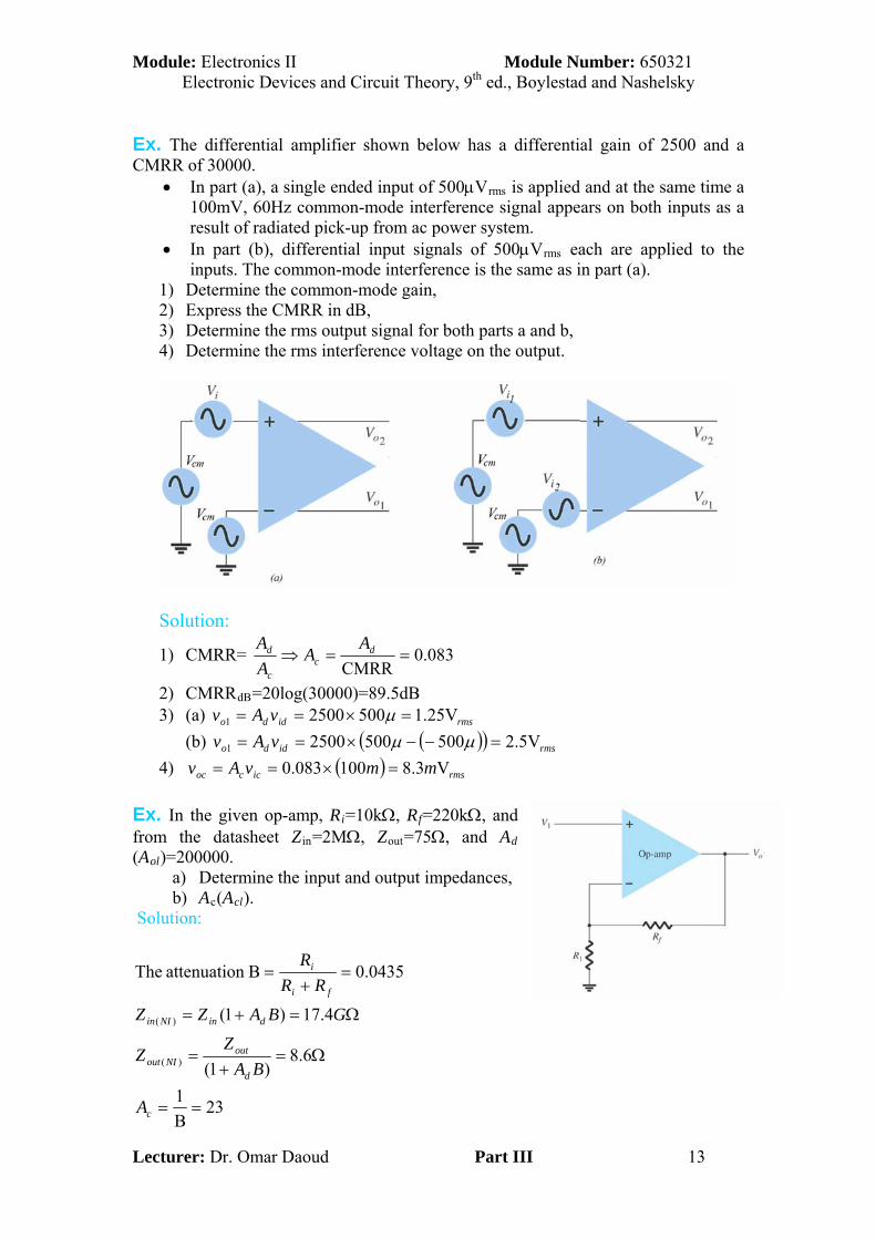
Ex. The differential amplifier shown below has a differential gain of 2500 and a CMRR of 30000.
In part (a), a single ended input of 500Vrms is applied and at the same time a 100mV, 60Hz common-mode interference signal appears on both inputs as a result of radiated pick-up from ac power system.
In part (b), differential input signals of 500Vrms each are applied to the inputs. The common-mode interference is the same as in part (a).
1) Determine the common-mode gain, 2) Express the CMRR in dB, 3) Determine the rms output signal for both parts a and b, 4) Determine the rms interference voltage on the output.
Solution:
1) CMRR= 083.0CMRR
dc
c
d AA
A
A
2) CMRRdB=20log(30000)=89.5dB 3) (a) rmsiddo vAv V25.150025001
(b) rmsiddo vAv V5.250050025001
4) rmsiccoc mmvAv V3.8100083.0
Ex. In the given op-amp, Ri=10k, Rf=220k, and from the datasheet Zin=2M, Zout=75, and Ad (Aol)=200000.
a) Determine the input and output impedances, b) Ac(Acl).
Solution:
23B
1
6.8)1(
4.17)1(
0435.0Bn attenuatio The
)(
)(
c
d
outNIout
dinNIin
fi
i
A
BA
ZZ
GBAZZ
RR
R
Lecturer: Dr. Omar Daoud Part III 13
Module: Electronics II Module Number: 650321 Electronic Devices and Circuit Theory, 9th ed., Boylestad and Nashelsky
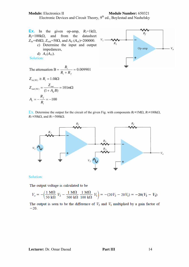
Ex. In the given op-amp, Ri=1k, Rf=100k, and from the datasheet Zin=4M, Zout=50, and Ad (Aol)=200000.
c) Determine the input and output impedances,
d) Ac(Acl). Solution:
100
101)1(
0.1
009901.0Bn attenuatio The
)(
)(
i
fc
d
outNIout
iNIin
fi
i
R
RA
mBA
ZZ
kRZ
RR
R
Ex. Determine the output for the circuit of the given Fig. with components Rf =1M, R1=100k, R2 =50k, and R3 =500k.
Solution:
Lecturer: Dr. Omar Daoud Part III 14

Module: Electronics II Module Number: 650321 Electronic Devices and Circuit Theory, 9th ed., Boylestad and Nashelsky
Op-Amps Applications (Active Filters):
A filter circuit can be constructed using passive components: resistors and capacitors. An active filter additionally uses an amplifier to provide voltage amplification and signal isolation or buffering (The high input impedance of the op-amp prevents excessive loading of the driving source. and the low output impedance of the op-amp prevents the filter from being affected by the load that it is driving. Active filters are also easy to adjust over a wide frequency range without altering the desired response). A filter that provides a constant output from dc up to a cutoff frequency
fOH and then passes no signal above that frequency is called an ideal low-pass filter.
A filter that provides or passes signals above a cutoff frequency fOL is a
high-pass filter.
When the filter circuit passes signals that are above one ideal cutoff
frequency and below a second cutoff frequency, it is called a bandpass filter.
Lecturer: Dr. Omar Daoud Part III 15

Module: Electronics II Module Number: 650321 Electronic Devices and Circuit Theory, 9th ed., Boylestad and Nashelsky
Active Low Pass Filters (LPF):
First Order LPF:
112
1
1
CRf
R
RA
OH
G
Fv
Second Order LPF:
22112
1
CRCRfOH
Lecturer: Dr. Omar Daoud Part III 16

Module: Electronics II Module Number: 650321 Electronic Devices and Circuit Theory, 9th ed., Boylestad and Nashelsky
Active High Pass Filters (HPF):
Active Band Pass Filters (BPF):
Lecturer: Dr. Omar Daoud Part III 17

Module: Electronics II Module Number: 650321 Electronic Devices and Circuit Theory, 9th ed., Boylestad and Nashelsky
d
Ex. For the given Active BPF circuit, if R1=R3=30k, R2=R4=51k, RA2=RB2=10k, RA1= 15k, RB1=30k, C1= C2= C3=0.01F and C2= 0.02 F then fin
a) The circuit BW, b) The geometric center frequency, and c) The Q value (Quality factor is defined as the peak energy stored in the
circuit divided by the average energy dissipated in it per cycle at resonance).
Solution:
42.2BW
921
380BW
11302
1)(
7502
1)(
21
12
2222
2
1111
1
o
cco
cc
BABA
c
BABA
c
fQ
Hzfff
Hzff
HzCCRR
LPFf
HzCCRR
HPFf
Lecturer: Dr. Omar Daoud Part III 18
Module: Electronics II Module Number: 650321 Electronic Devices and Circuit Theory, 9th ed., Boylestad and Nashelsky
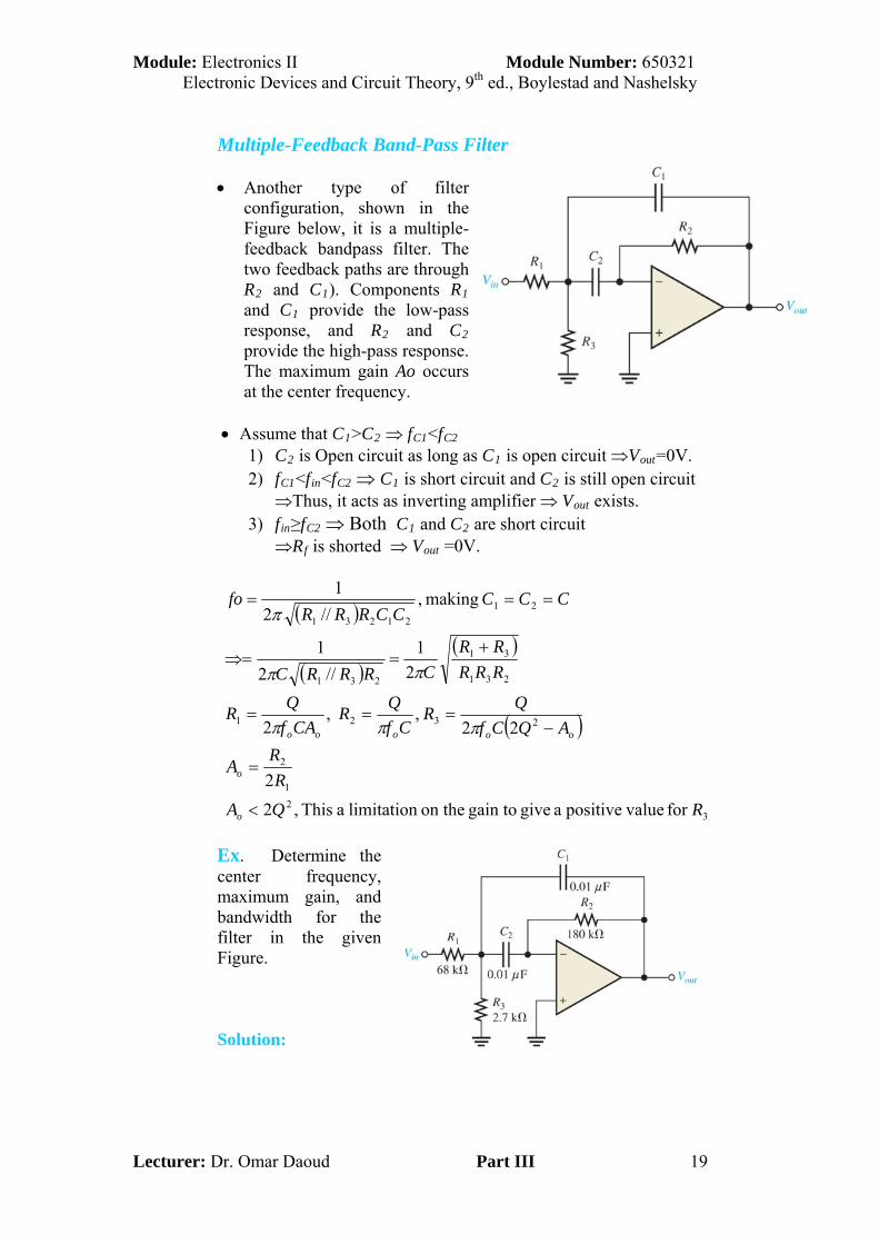
Multiple-Feedback Band-Pass Filter Another type of filter
configuration, shown in the Figure below, it is a multiple-feedback bandpass filter. The two feedback paths are through R2 and C1). Components R1 and C1 provide the low-pass response, and R2 and C2 provide the high-pass response. The maximum gain Ao occurs at the center frequency.
Assume that C1>C2 fC1<fC2 1) C2 is Open circuit as long as C1 is open circuit Vout=0V. 2) fC1<fin<fC2 C1 is short circuit and C2 is still open circuit Thus, it acts as inverting amplifier Vout exists. 3) fin≥fC2 Both C1 and C2 are short circuit Rf is shorted Vout =0V.
32
1
2
2321
231
31
231
21
21231
for valuepositive a give gain to on the limitation a This ,2
2
22 , ,
2
2
1
//2
1
making ,//2
1
RQA
R
RA
AQCf
QR
Cf
QR
CAf
QR
RRR
RR
CRRRC
CCCCCRRR
fo
o
o
ooooo
Ex. Determine the center frequency, maximum gain, and bandwidth for the filter in the given Figure. Solution:
Lecturer: Dr. Omar Daoud Part III 19

Module: Electronics II Module Number: 650321 Electronic Devices and Circuit Theory, 9th ed., Boylestad and Nashelsky
Lecturer: Dr. Omar Daoud Part III 20
Hz1774.16
Hz736BW
16.418001.0Hz736
32.1)68(2
180
2
Hz7367.218068
7.268
)01.0(2
1
2
1
2
1
2
231
31
Q
fo
kFCRfQ
k
k
R
RA
kkk
kk
FRRR
RR
Cfo
o
o
Active Notch/Band-Stop Filters (NF):
1) fin<fC2 C1 and C2 is open circuit Vout=0V from the inverting
stage but there is a noninverting one. 2) fC1<fin<fC2 C1 is short circuit Vi is shown to be common
mode signal.
3) fin≥fC2 Both C1 and C2 are short circuit C2 is short out the signal at inverting input Vout comes from
the noninverting input (amplify the difference between the two inputs).
1 ,2
1
2121
oACCRR
fo