operational amplifier circuit for hi fi tecnici/jbl - operational... · operational amplifier...
TRANSCRIPT
Operational Amplifier
Circuit for Hi Fi
Reprinted from ELECTRONICS WORLD,
JANUARY 1967
B y B . N . L O C A N T H I / Vice President, Engineering. James B. Lansing Sound, Inc.

Front-panel view of new "T-circuit" integrated stereo amplifier unit.
Operational Amplifier
Circuit for Hi-Fi B y B. N . L O C A N T H I / Vice President, Engineering, lames B. Lansing Sound, Inc.
Technical details on the ''T circuit" as employed in the new JBL ultra-low distortion audio power amplifier.
A S we gain more and more insight into the performance i\ of the human ear, the design of sound recording and
] _ \_ reproducing apparatus grows correspondingly more sophisticated. Whereas the critical audiophile was once satisfied if his power amplifier could produce 10 watts at 1000 Hz with less than 1% distortion, he now expects at least 25 watts per stereo channel with less than 0.5% distortion at any frequency from 20 to 20,000 Hz.
By making full use of today's electronic technology, it is possible to build an audio amplifier of such quality that its complete performance cannot be accurately measured, even with the best test equipment presently available. The "T circuit" developed by the author is such an amplifier.
In a number of respects, the "T circuit" is unusual, and a United Slates patent is pending on the circuit. The basic design philosophy, however, is an old one worth restating. W e believe that an amplifier should be designed for low distortion and wide bandwidth without feedback. Negative feedback is then added to make an already good design perform even better; it is not used to "clean up" problems in the basic design.
Some engineers think this is an old-fashioned idea. They feel that by using great amounts of negative feedback, desired performance can be obtained even from essentially non-linear amplifying circuits, and that it is the performance of the complete design that counts. This approach can result in an amplifier which has impressive figures in all of the standard specifications but which develops serious performance faults when more elaborate testing techniques are used.
In the circuit to be described, the operating parameters of every stage are chosen for maximum transfer linearity, which is just another way of saying lowest possible distortion. And the operating mode of each stage is held constant, irrespective of signal level. This means that we don't "shift gears" to take care of varying power levels, nor do we
try to make the circuit "pretend" it is doing something which in fact it is not.
The Amplif ier Circuitry The output circuit of the amplifier (Fig. 1) consists of
three cascaded complementary-symmetry emitter-follower stages. The configuration has somewhat the appearance of a biidged-T circuit, which accounts for its name.
The advantages of the complementary-symmetry emitter-follower output stage, using one p-n-p and one n-p-n transistor, are well known. Its output impedance is low so that loads in the 4- to 16-ohm range can be driven without the need for an output transformer. Transistor idling current can be controlled so that the efficiency of elass-B operation is approached but without the notch distortion common to dass-B amplifiers.
Most important, the complementary-symmetry configu-
Fig. 1. Three-stage output circuit. Note "T" configuration.
INPUT
O U T P U T
+ 4 5 V - 4 5 V
+ 40V
+ 3 5 V
- 4 0 V
- J 5 V
ration does not require a separate phase-splitter stage. When a signal is applied to the common driving point, one transistor draws more current and the other draws less. In the "T circuit," the three cascaded emitter-followers in each group all operate together as if the output circuit were a single stage. (In practice, the transistors are biased close to cut-off so that one group conducts primarily during positive half-cycles while the other group conducts mainly during negative half-cycles.)
What are the special advantages of this arrangement? First, the output circuit has exceptionally low drive requirements. While the emitter-follower has no voltage gain, it does provide considerable power gain. In this respect, it is similar to the familiar vacuum-tube cathode follower. The three output stages multiply output load impedance by a factor of 100,000 as it is reflected back to the collector driving point. Even though voltage gain is less than unity (about 0 .9) , the power gain of the three stages is therefore almost 100,000.
Another important characteristic of the circuit is its excellent thermal stability. Output transistors 0 5 and 0 6 are connected directly to a high-current power supply of about 35 volts plus and minus potential. Each base of the output stage has a low-resistance path for the collector-to-base leakage current to flow through its opposite emitter driver stage. Because the input driver collector load resistance is about 9000 ohms and because the output load impedance is multiplied by a factor of 100,000, the d.c. stability factor of the circuit is better than 10. Thus, d.c. thermal runaway problems are essentially non-existent.
A single bias supply consisting of diodes Dl through D5 provides the necessary forward bias for all three cascaded emitter-followers. The bias supply operates at a low current level and dissipates very little signal power, yet it provides all the advantages of diode biasing.
One disadvantage of the circuit is that successively higher collector supply voltages are required for each driver stage to take care of the saturation voltage drops of the preceding transistors. The individual supply voltages are indicated in Fig. 1.
This requirement leads to a rather complicated-looking power supply but not an inordinately expensive one. By using two additional low-current secondary windings for the driver power supplies, a symmetrical "package" is obtained which turns out to be somewhat smaller, physically, than would be expected for an 80-watt amplifier.
Performance of Output Stages Before going into details of the associated driver stages,
let's take a brief look at the performance of the output circuit alone. Because each pair of transistors has a higher beta cut-off frequency than the following pair, the over-all frequency limitation of the circuit is determined almost entirely by Q5 and Q6, and the bandwidth of the three cascaded stages turns out to be greater than 100,000 Hz. With this kind of frequency response, the classic textbook rules regarding reduction of distortion and noise by negative feedback do apply, as we shall see a little further on.
Distortion measurements of the output circuit without feedback indicate that at very low signal levels, total harmonic distortion stabilizes at about 0.2% or 0.3% and then increases to about 2.5% at 50 watts output per channel. This certainly is not phenomenal in itself, but remember that we are talking about performance without feedback.
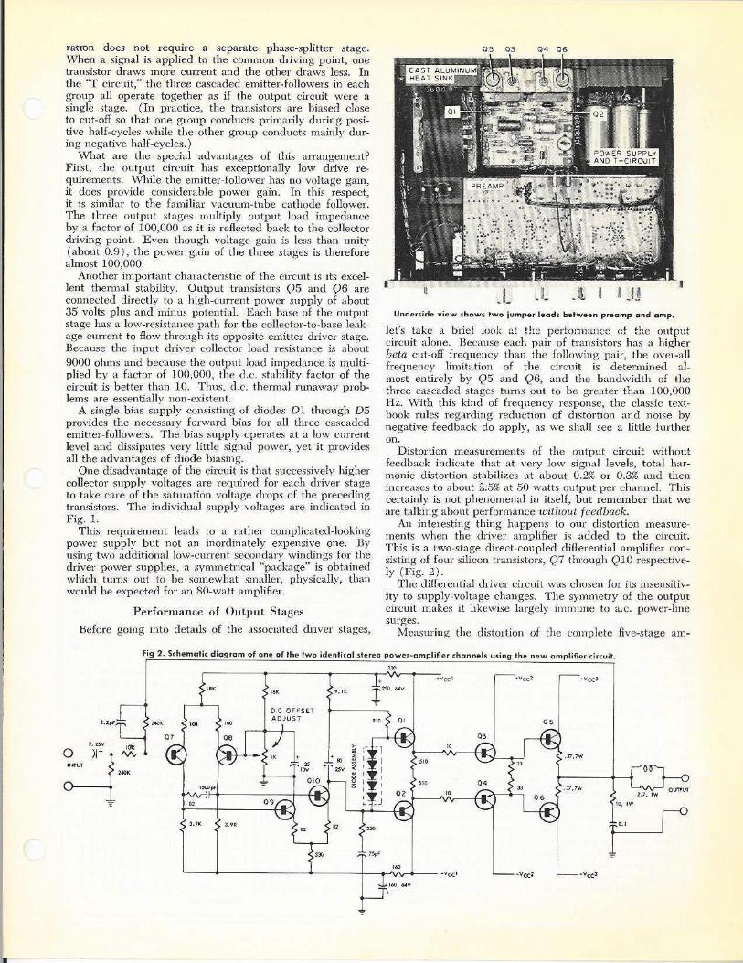
An interesting thing happens to our distortion measurements when the driver amplifier is added to the circuit. This is a two-stage direct-coupled differential amplifier consisting of four silicon transistors, Ql through Q10 respectively (Fig. 2 ) .
The differential driver circuit was chosen for its insensitiv-ity to supply-voltage changes. The symmetry of the output circuit makes it likewise largely immune to a.c. power-line surges.
Measuring the distortion of the complete five-stage am-
Fig 1. Schematic diagram of one of the two identical stereo power-amplifier channels using the new amplifier circuit.
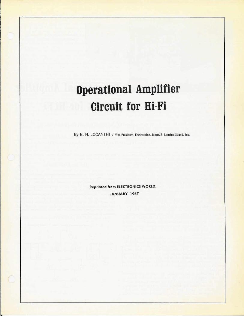
Underside view shows two jumper leads between preamp and amp.
INPUT
OUTFUT
D C . OFFSET ADJUST

plifier, still without feedback, we find that the figures are lower than for the output circuit alone! Harmonic distortion at ]()()() Hz and 50 watts output measures less than 1%. Even at 20,000 Hz the circuit produces only about 1.5% distortion (Fig. 3 ) .
Why should the distortion of the whole amplifier be less than that of the output circuit alone? It may be that the distortions of individual stages tend to be slightly complementary, but the main reason appears to be that we are now driving the output circuit with a partial-current generator instead of a zero-ohms source impedance.
Now let's see what happens when the feedback loop is connected. Fig. 2 is a schematic of one channel of the complete stereo power amplifier. Note that the only coupling capacitor is located at the input and that from this point on the entire power amplifier is direct-coupled. Also note that the feedback loop extends all the way from the output of the amplifier back to the input terminals. No stage, no part of any stage, is left outside the feedback loop.
The circuit therefore falls into the classification of d.c. operational amplifiers, devices that are widely used in telemetry and computer applications. Properly designed, such an amplifier can be made to exhibit unconditional stability under any load condition and to maintain uniform gain and low distortion down to d.c. The marginal stability at subsonic frequencies which afflicts many amplifier designs is notably absent.
When we try to pin down the performance of the complete circuit, a rather interesting problem arises. In essence, the amplifier is as good as or belter than any available test equipment. For example, we know that the total harmonic distortion of the amplifier without feedback is about 0.5% at 1000 Hz when the amplifier is producing 30 watts into an 8-ohm load. With a feedback factor of 50, distortion should be reduced proportionately, resulting in a figure of about 0.01%.
But even with the most sensitive equipment and the greatest care in excluding stray signals from the test hookup, distortion can be measured accurately only down to 0.015% or so. Because of this, the measurements graphed in Figs. 4 and 5 are probably accurate only where the curves climb above 0.05%. Until the circuit is driven into clipping, distortion is so low that it cannot be specified with any degree of exactness.
Fig. 6 shows the frequency response of the complete amplifier at 40 watts and one watt and with an open output circuit. The open-circuit response curve cannot be seen because it lies exactly along the one-watt curve, showing that the open-circuit stability of the amplifier is excellent.
The circuit is stable under any passive load, resistive or reactive. The inductor (actually only a few turns of very low resistance wire) in series with the output is sufficient to act as a buffer for certain capacitive loads which might otherwise cause some ringing. Even without the inductor, however, the circuit will not oscillate.
Overload Protection W e have already explained that the amplifier's design
makes it largely immune to a.c. line-voltage surges. Its performance when momentarily overdriven is equally impressive. The circuit recovers from a 100% single-cycle overload in less than one-tenth of a cycle—at any frequency from 20 to 20,000 Hz. As far as we have been able to determine, the unit recovers almost instantly from any overload at any frequency inside or outside the audio spectrum.
What about prolonged overload, such as might result from accidentally shorted loudspeaker connections? The output transistors used in commercial versions of this circuit have a d.c. power dissipation capability of about 150 waits each. Il should be emphasized that this refers to continuous power, not brief pulses. Because of this high power dissipa-
PRINTED IN U S A.
Fig. 4. Harmonic distortion with feedback loop connected.
tion capability, no exotic high-speed protective devices are required. The output circuit lias a thermal breaker (not shown in the schematic) which opens in one to 60 seconds if excessive current is drawn. This is all that is needed to protect the output transistors in the event of a short circuit.
As long as the amplifier is operated within the maximum current-handling capacity of the output stage, any kind of loudspeaker system, with almost any impedance rating, can be connected without degrading the signal quality.
As described in this article, the " T circuit" is used in the JBL Model SA-600 preamplifier/amplifier. It is also found in JBL Models SE-400S and SE-408S. These are sophisticated power amplifiers called "Enei gizei s" because their performance is tailored to match the requirements of the particular loudspeaker systems with which they are used.
In all three models, however, the "T circuit" provides 80 watts of continuous sine-wave power (40 watts per channel) with both channels operating simultaneously, with power-line voltage as low as 110 volts, and with less than 0.2% distortion at any frequency from 20 to 20,000 Hz .
Coeyrlfht 9 by Zlfl-Davli Publishing Company. All rlshts i r H r v M .
PE
RC
EN
T
HA
RM
. 0
IST
.
P O W E R O U T P U T ( W A T T S ) INTO S - O M M LOAO
Fig. 3. Harmonic distortion of power amplifier without feedback.
POWER O U T P U T ( W A T T S ) INTO 8 - O M M L O A D
PE
RC
EN
T
HA
RM
. 0
IST
.
Fig. 5. Intermodulation distortion with feedback connected.
EQUIVALENT S I N E - W A V E P O W E R - W A T T S
PE
RC
EN
T
IM 0
IST
. R
ELA
TIV
E R
ES
PO
NS
E-i
je
Fig. 6. Frequency response into open circuit and 8-ohm load. The input coupling capacitor has been shorted out to show the good low-frequency performance of the complete amplifier.
F R E Q U E N C E - H I
I WATT ANO 1
OPEN CIRCUIT