operation of a modular multilevel converter (m2lc) in ... · operation of a modular multilevel...
TRANSCRIPT

Operation of a Modular Multilevel Converter (M2LC)
in Resonance Mode(Rev. C)
Michael E. Aiello5/4/2014
mailto:[email protected]
Revision C12/27/2014
Revision History:
Revision A (7/14/2014) Added section Resonance Operation at Intermediate Levels starting on page 22.
Revision B (8/22/2014) Modified section Resonance Operation at Intermediate Levels to include two examples of modulation. Also, the part of the simulatorresponsible for simulating the switching devices was dissipating too much power on turn-on. This resulted in an abnormal amount of discharge on the cell capacitors. The turn-on spikes are now more representative of an actual IGBT (or MOSFET) commutating a forward conducting diode. Also, added Acknowledgment and Provisional Patent Application sections at the end of this document.
Revision C (12/27/14) Remove clause Provisional Patent Application from Revision B. All information contained in this document is now part of the public domain.

Abstract
The discussion of a technique for producing DC or low frequency AC at the output of a modular multilevel converter (M2LC) while maintaining voltage equilibrium on all cells. This technique uses anintermediate mode of modulation for at or near static conditions (a three phase machine operating at zero or low frequency while producing torque). In normal operation, an inter-digitizing PWM is engaged, which is the typical operating mode in an M2LC control system.
This approach relies on each leg of the converter operating at resonance dictated by the average value of cell capacitance, the value of the interface inductance, and the fundamental modulation carrier.In this mode, all cells remain balanced providing for a smooth transition into inter-digitizing mode when the speed of the machine is at a point where the voltages on each of the cells can be maintained with minimum voltage ripple.
Background
The normal operating mode of an M2LC converter allows only the control of AC current and voltage to a load1. Under standard operating conditions, DC control is not possible. Low frequency operation is possible only if the cell capacitance is sufficiently large.
These factors obviously pose a problem for use in the control of AC motors in process control. Some novel solutions have been presented to over come this limitation. One such solution is to have theconverter operate in a quasi two level mode at zero or low frequency. Here the switching wave form takes on the characteristics of both two level and mult-level, the portion of which dictated by the amount of zero or low frequency power control required2.
In reality, the physics of the system require that there must be some characteristic of two level imposed in the switching waveform in order to sustain DC or low frequency AC operation. The quality of the waveform and the ability to have strict control of cell voltages at all times when operating in this mode is paramount since there must be a smooth transition back to the classical switching mode of the M2LC when conditions warrant (erg., the load frequency is sufficiently high enough to allow this).
Contained in this document are snapshots of switching waveforms of one phase of a M2LC system. These waveforms were produced by a special simulation program constructed to allow easy manipulation of control variables. This simulator was written in C++ to implement a SPICE model of one phase of M2LC system. It was written brute force in that no variable time step mode was used and no use of sparse matrices to speed simulation time. The entire M2LC circuit (single phase) is represented in one 69 x 70 matrix.
To validate this solver, a special load was constructed so as to make it easily representable in a mainstream SPICE solver such as NG-SPICE. Both solvers were then run and results compared. The details of this test are presented in Appendix A.
1 For this paper, the assumption is the M2LC consists of three independently controlled phases connected to an an AC motor or load. Except where noted, this paper focuses on the operational characteristics of only one of these phases.
2 A patent for this technique is held by Curtiss-Wright Corporation.

The effectiveness of the C++ implemented solver became apparent when implementing the various tests presented in this paper. In traditional SPICE it is very difficult to construct elaborate signal generating schemes like those presented in this paper.
Simulation is based on the model shown in Figure 1. This diagram depicts one phase of a 5-Level M2LC system. The bias is a +/- 1000 VDC zero impedance source. In an actual implementation, three converters would be connected in parallel and sourced by a bridge rectifier. The source to this rectifier would possess some sort of impedance. As a result, phase-to-phase interaction would be present. For this paper, these effects are not represented.
The parameters for this model (and all tests in this paper unless otherwise noted) are listed in Table 1. Except for the simulations shownin Appendix A, all simulations were done using an ideal current source load applied at ia in Figure 1 . This was done because most of the tests shown below (all except those of Figure 2, 3 and 27) were performed atzero operating frequency, our worst case condition.
The simulation also models the affect of dead time (or gate delay).This was set at 1 uSec for all test cases. The effect can be seen in some of the plots below as voltage spikes of a polarity dictated by the direction of applied current at ia. In Figure 1, Rp and Rn were added only to provide stability in the simulation program.
The fundamental switching frequency of the converter was set at 1 KHz. With 5 levels, this translate to an overall switching frequency of 4Khz. For simplicity, the switching elements S<xx> (which would normally be IGBT's) are shown as MOSFETS and modeled as gate controlled variable resistors with predefined slew rate.
The elements D<xx> are also modeled as variable resistors, but under the control of the direction of current flow through them.
C1 through C8 400 uF
S11 through S82 .1 Ohm "On" - 1 Mega-ohm "Off" resistance.Gate Delay – 1 uSecOn/Off conduction rate - 1e10 Ohms/SecCapacitance - .1 uF
D11 through D82 .1 Ohm "On" - 1 Mega Ohm "Off" resistance.
Lp and Ln .25 mH
Rp and Rn 10000 Ohms (for simulation stability only)
Switch Frequency(Normal Mode)
1 KHz Fundimental (4 KHz, 5 Level)
Table 1 Figure 1
S11
S12
D11
D12
C1
S21
S22
D21
D22
C2
S31
S32
D31
D32
C3
S41
S42
D41
D42
C2
Lp
Ln
Rp
Rn
S51
S52
D51
D52
C5
S61
S62
D61
D62
C6
S71
S72
D71
D72
C7
S81
S82
D81
D82
C8
+1000 VDC
-1000 VDC
MLvl_vs_a
(MLvl_vs_b and MLvl_vs_c in Figure 21,22 and 23)
ia
MLvl_ipl
MLvl_inl
MLvl_i2
Normal Mode
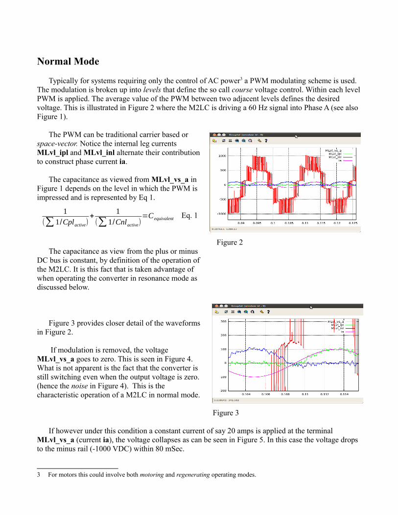
Typically for systems requiring only the control of AC power3 a PWM modulating scheme is used. The modulation is broken up into levels that define the so call course voltage control. Within each levelPWM is applied. The average value of the PWM between two adjacent levels defines the desired voltage. This is illustrated in Figure 2 where the M2LC is driving a 60 Hz signal into Phase A (see also Figure 1).
The PWM can be traditional carrier based or space-vector. Notice the internal leg currents MLvl_ipl and MLvl_inl alternate their contributionto construct phase current ia.
The capacitance as viewed from MLvl_vs_a in Figure 1 depends on the level in which the PWM is impressed and is represented by Eq 1.
Eq. 1
Figure 2
The capacitance as view from the plus or minus DC bus is constant, by definition of the operation ofthe M2LC. It is this fact that is taken advantage of when operating the converter in resonance mode as discussed below.
Figure 3 provides closer detail of the waveformsin Figure 2.
If modulation is removed, the voltage MLvl_vs_a goes to zero. This is seen in Figure 4. What is not apparent is the fact that the converter is still switching even when the output voltage is zero.(hence the noise in Figure 4). This is the characteristic operation of a M2LC in normal mode.
Figure 3
If however under this condition a constant current of say 20 amps is applied at the terminal MLvl_vs_a (current ia), the voltage collapses as can be seen in Figure 5. In this case the voltage drops to the minus rail (-1000 VDC) within 80 mSec.
3 For motors this could involve both motoring and regenerating operating modes.
1(∑ 1/Cplactive)
+1
(∑ 1/Cnlactive)=C equivalent

Herein lies the problem with M2LC converters when applied to applications such as motors used in position control or motors that require low speed operation. Some solutions have been proposed to add an auxiliary mode to operate the converter at low frequency (or static) conditions.
One such solution is to add a mode that partially places the converter in a quasi 2-Level mode such that a portion of the plus and minus bus voltages are impressed on the motor lead every switch cycle4. In this approach, 2-Level operation is gradually added to the traditional PWM to provide high current at DC or low frequency operation. As the frequency is increased, this auxiliary mode is phased-out.
This is very effective in providing high power to
the motor phase while reducing the discharge effect of the leg capacitors.
The approach however is brute-force in the sense that the controllability of the capacitor voltages is lost while operating in this mode. This isan important factor because of the need for a smooth transition back to the traditional (M-Level) switching pattern when the load frequency is sufficiently high enough to maintain control of voltages on the capacitors.
Figure 4There needs to be a solution such that rail-to-
rail 2-level switching can be effectively impressed on the load while at the same time maintaining complete control of the capacitor voltages and currents.
The drawback however in doing this requires current flow to be maintained between the plus and minus bus connections while at the same time controlling current to the motor terminal.
This increases the total current flow through IGBT's and capacitors.
Figure 5
Papers have been presented in regards to adding a balancing mechanism to the standard control algorithm for the purposes of maintaining equally distributed capacitor voltages while operating a low frequency5.
4 This approach is held by a patent belonging to Curtiss-Wright Corperation.5 “Inner Control of Modular Multilevel Converters – An Approach using Open-loop Estimation of Stored Energy”,
Angquist, Antonopoulos. “On Dynamics and Voltage Control of Modular Multilevel Converter”, Angquist, Antonopoulos
Resonance Mode
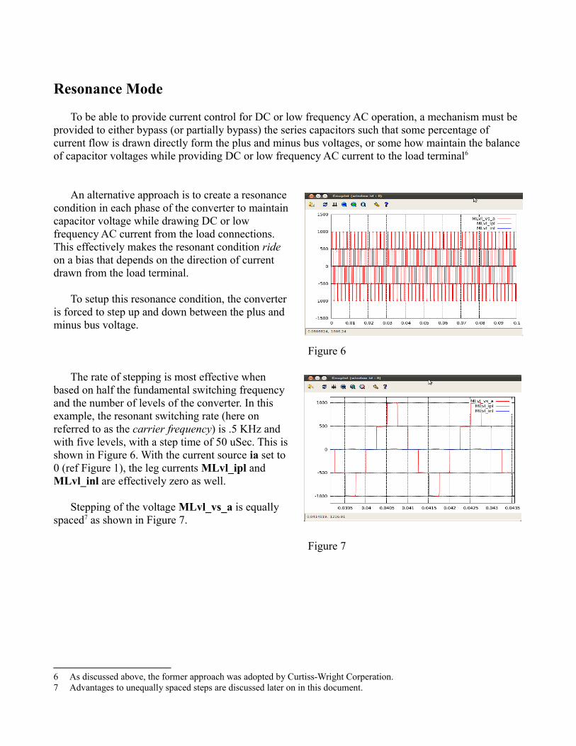
To be able to provide current control for DC or low frequency AC operation, a mechanism must be provided to either bypass (or partially bypass) the series capacitors such that some percentage of current flow is drawn directly form the plus and minus bus voltages, or some how maintain the balance of capacitor voltages while providing DC or low frequency AC current to the load terminal6
An alternative approach is to create a resonance
condition in each phase of the converter to maintaincapacitor voltage while drawing DC or low frequency AC current from the load connections. This effectively makes the resonant condition ride on a bias that depends on the direction of current drawn from the load terminal.
To setup this resonance condition, the converter is forced to step up and down between the plus and minus bus voltage.
Figure 6
The rate of stepping is most effective when based on half the fundamental switching frequency and the number of levels of the converter. In this example, the resonant switching rate (here on referred to as the carrier frequency) is .5 KHz and with five levels, with a step time of 50 uSec. This isshown in Figure 6. With the current source ia set to 0 (ref Figure 1), the leg currents MLvl_ipl and MLvl_inl are effectively zero as well.
Stepping of the voltage MLvl_vs_a is equallyspaced7 as shown in Figure 7.
Figure 7
6 As discussed above, the former approach was adopted by Curtiss-Wright Corperation.7 Advantages to unequally spaced steps are discussed later on in this document.

An FFT of the signal in Figure 8 is shown in Figure 8. With no loading there is no DC component present.
Figure 8
Next, the current source ia is set to 20.0 amps. Referring now to Figure 9 (with a close-up view near the time reference at 40 mSec shown in Figure 10), the oscillating leg currents MLvl_ipl and MLvl_inl now begin to appear with an offset of 20.0 amps.
Figure 9 Figure 10
These currents are roughly sinusoidal with ripple caused by the voltage step changes as viewed form the load terminal. Under Ideal conditions, MLvl_ipl would peak between +40 amps and 0. MLvl_inl would peak between +20 amps and -20 amps with + 20 amps DC drawn form Mlvl_ipl (current ia in Figure 1).

A DC voltage component of approximately -28 volts at the load terminal MLvl_vs_a now begins toappear as shown in Figure 118
`
Figure 11
The bias is negative because we are drawing current from terminal MLvl_vs_a. Each of the steps contain this negative bias (see Figure 9). With the help of the inter-phase inductance Lp and Ln to soften the peak charging of capacitors C1 through C8, the system re-balances and maintains operation without discharging the capacitors unlike that of the condition described for Figure 5 above.
8 Note that for case of all FFT plots shown in this document, a Single-Sided algorithm is used making the amplitudes of the DC components appear to be twice there actual amplitude and always positive.

Resonance Mode with Controlled Bias
Modifying the base carrier signal defined in Figure 7 to provide a plus bias will allow the load induced bias in Figure 9 and 10 to be canceled. If enough bias is added, the load bias can be reversed from a negative voltage to a positive voltage9. This is shown in Figure 12 and with detail in Figure 13.
Figure 12 Figure 13
Notice the peak magnitudes of MLvl_ipl and MLvl_inl actually drop (compare Figure 10 and Figure 13) close to there ideal value.
Figure 14
For the signal shown in Figure 12, approximately +125 VDC of command voltage is added to produce approximately +100 of bias as indicated by the FFT of this signal shown in Figure 1410.
9 The discussion of the method used to add bias to the base signal shown in Figure 7 to produce the signal in Figure 12 is beyond the scope of this document. A variety of approaches can be used. For this simulation, a multi-level PWM reference was created to add and subtract command voltage at preselected points on the base carrier signal.
10 A simple calculation can be used to compute the drop caused by the discharging capacitors. Vdrop = .5*I*T/C = 25 VDC where C is the cell capacitance (in this case 400 uF), T=.001 and I=20.0. This approximation does not hold for high values of current ia.
Application of Bias
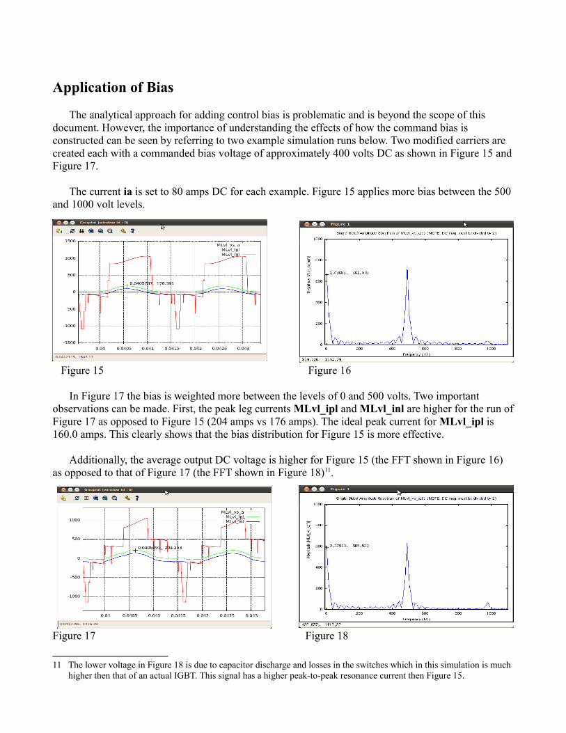
The analytical approach for adding control bias is problematic and is beyond the scope of this document. However, the importance of understanding the effects of how the command bias is constructed can be seen by referring to two example simulation runs below. Two modified carriers are created each with a commanded bias voltage of approximately 400 volts DC as shown in Figure 15 andFigure 17.
The current ia is set to 80 amps DC for each example. Figure 15 applies more bias between the 500 and 1000 volt levels.
Figure 15 Figure 16
In Figure 17 the bias is weighted more between the levels of 0 and 500 volts. Two important observations can be made. First, the peak leg currents MLvl_ipl and MLvl_inl are higher for the run ofFigure 17 as opposed to Figure 15 (204 amps vs 176 amps). The ideal peak current for MLvl_ipl is 160.0 amps. This clearly shows that the bias distribution for Figure 15 is more effective.
Additionally, the average output DC voltage is higher for Figure 15 (the FFT shown in Figure 16) as opposed to that of Figure 17 (the FFT shown in Figure 18)11.
Figure 17 Figure 18
11 The lower voltage in Figure 18 is due to capacitor discharge and losses in the switches which in this simulation is much higher then that of an actual IGBT. This signal has a higher peak-to-peak resonance current then Figure 15.
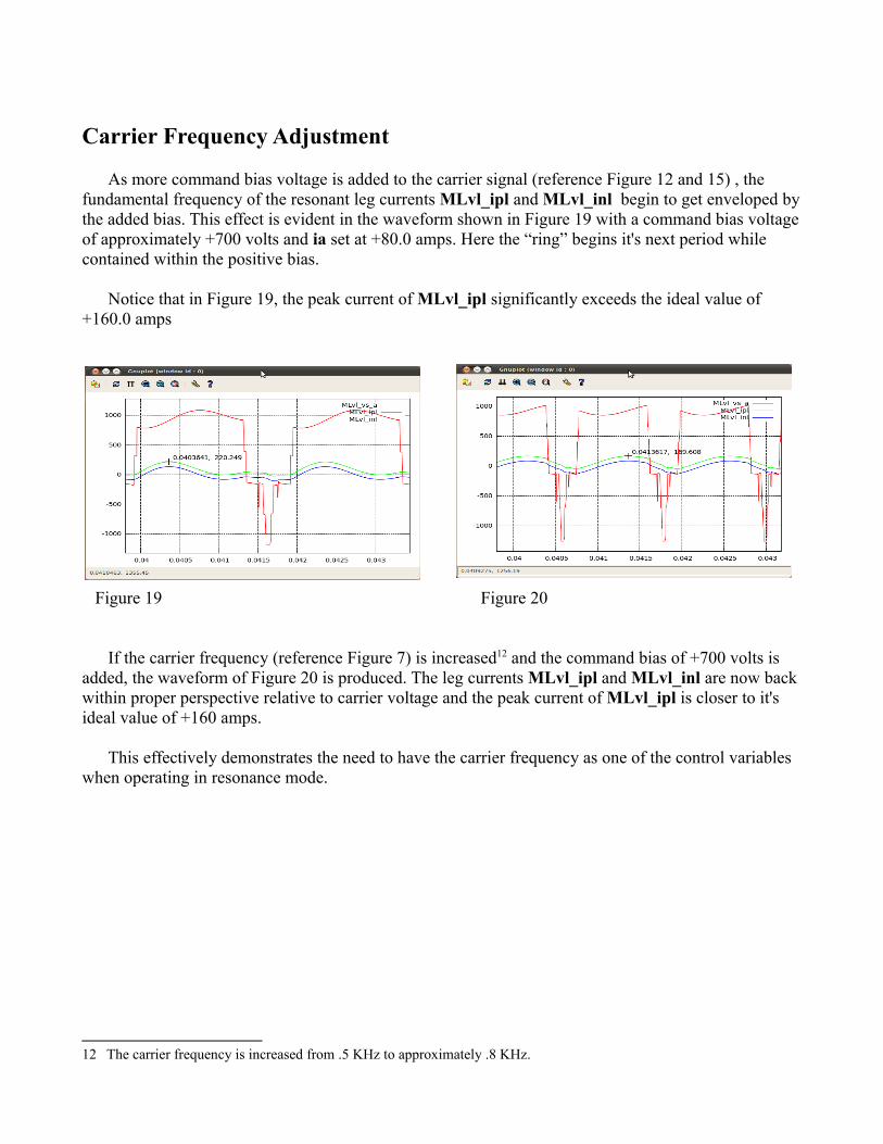
Carrier Frequency Adjustment
As more command bias voltage is added to the carrier signal (reference Figure 12 and 15) , the fundamental frequency of the resonant leg currents MLvl_ipl and MLvl_inl begin to get enveloped bythe added bias. This effect is evident in the waveform shown in Figure 19 with a command bias voltageof approximately +700 volts and ia set at +80.0 amps. Here the “ring” begins it's next period while contained within the positive bias.
Notice that in Figure 19, the peak current of MLvl_ipl significantly exceeds the ideal value of +160.0 amps
Figure 19 Figure 20
If the carrier frequency (reference Figure 7) is increased12 and the command bias of +700 volts is added, the waveform of Figure 20 is produced. The leg currents MLvl_ipl and MLvl_inl are now back within proper perspective relative to carrier voltage and the peak current of MLvl_ipl is closer to it's ideal value of +160 amps.
This effectively demonstrates the need to have the carrier frequency as one of the control variables when operating in resonance mode.
12 The carrier frequency is increased from .5 KHz to approximately .8 KHz.

Application of Multi-phase Bias
Currently, the simulation program used with this document can produce only single phase plots. Load currents (ia in this case, reference Figure 1) are modeled as either a DC or AC current source. However, by manipulating the parameters for load currents and the voltage bias commands, three independent simulation runs can be made with the outputs superimposed for the purpose on gaining insight into how the output load of an actual three phase M2LC would look running in resonant mode.
This is shown in the following figures. Figure 21 represents the output of the three phase M2LC at no load. In this case all three terminal voltages overlap. Consequently, there is no noticeable line-to-line voltage impressed on the three terminal connections.
Figure 21
For Figures 22 and 23, bias voltage and load current is added in such a way as to represent a snapshot in time of a commutated rotating machine (AC motor) connected to the converter.
Figure 22 Figure 23
The waveform shown in Figure 22 is indicative for commutation of a machine operating at low frequency, with the waveform of Figure 23 for higher frequency.
Some important points must be made relative to the waveforms shown in Figure 22 and 23. First, asstated above, the three phases are super-positions of a single phase simulations each with fixed load current and command bias voltages. Being the case, there is no modeling of the interaction of the three phases with respect to each other.

In an actual system, the fact the terminal voltages (MLvl_vs_a, MLvl_vs_b, and MLvl_vs_c) havemeasurable impedance suggests an interaction. Also, the model does not take into consideration the factthat in a real system the plus and minus bus voltages (+1000 VDC and -1000 VDC) are not low impedance sources13. This fact as well would alter the representations of Figure 22 and Figure 23.
However, what can be noted from these waveforms is the suggestion that control of the bias voltagewould be a result of some sort of space-vector algorithm as opposed to a simple PWM control.
In addition, it should be noted that the waveform of Figure 23 would not usually come into play if applied to a rotating machine load. The amount of bias voltage here suggest that the motor would be operating at a rotating frequency that would dictate the use of normal M2LC operation (see Figure 2).
13 Actually, the typical source is a bridge rectifier with some intrinsic inductance. The effective bus capacitance comes from the series connected cell switching in and out of the circuit, which is a constant.

Effects of Inter-phase Induction Selection
To establish an effective resonance operating mode for the M2LC, a suitable value for the inter-phase inductance Lp and Ln (see Figure 1) must be established. As mentioned above, the terminal capacitance (measured at MLlvl_vs_a) varies with the level as dictated by Eq. 1 above. However as viewed from the plus and minus bus, the capacitance in constant.
The resonant frequency is a simple calculation using Eq. 2 with Ceffective equal to 100 uF for all examples presented in this paper14.
f=1/(2∗π∗√(Lp+Ln)∗C effective) Eq. 2
With the carrier frequency selected at .5 KHz, Lp and Ln work out to be approximately .25 mH.
Figure 24 Figure 25
Consider now the value of Lp an Ln set to .02 mH as shown in Figure 24 above with detail shown in Figure 25. Excessive ripple appears on MLvl_ipl (and MLvl_inl, not shown). The load current ia is set to +20 amps with no commanded bias voltage, the same conditions as that shown in Figure 9 and 10above.
Current is still under control. However, significant power loss can be assumed due to the high ripple current.
14 Only four 400 uF capacitors are switched into the circuit at any given time.
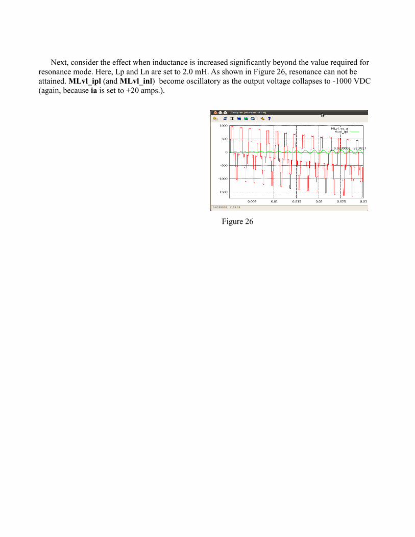
Next, consider the effect when inductance is increased significantly beyond the value required for resonance mode. Here, Lp and Ln are set to 2.0 mH. As shown in Figure 26, resonance can not be attained. MLvl_ipl (and MLvl_inl) become oscillatory as the output voltage collapses to -1000 VDC (again, because ia is set to +20 amps.).
Figure 26

Resonance to Normal Mode Transition
For the M2LC to be used in a three phase configuration for AC motor control requires the converterto operate at low modulation frequencies. In the discussion above, it is suggest that for low operating frequency (or even static DC torque control), the resonance mode be used.
For a given operating current, once the rotating frequency is high enough to prevent the link capacitors (C1 though C8 in Figure 1) from discharging to point that would cause excessive ripple in the leg currents (MLvl_ipl and MLvl_inl), the converter would switch (or transfer) to normal M2LC operation.
This transfer is demonstrated in Figure 27 for one of three phases of the converter.
Figure 27
Like the discussion for section Application of Multi-Phase Bias above, certain points about how the simulator was set up to demonstrate this condition must be noted.
First, like the section noted above, there is no modeling of the effects or interactions of the other two phases on terminal MLvl_vs_a. Unlike the simulation runs above, the voltage biasing command is sinusoidal. Also, the current ia is configured as an AC current source in phase with the biasing command.
The current ia is also phase shifted by an amount relative to the biasing command that would be indicative of a motoring action (power being drawn form the +/- 1000 VDC bus.
Operation is done open-loop, with no regard to control of the voltage at MLvl_vs_a, on during or after the transfer from resonance mode to normal mode. The bias command for both resonance mode and normal command mode was setup to generate approximately +/- 125 volts peak amplitude.
The peak amplitude of the AC current source was set to +/- 20 amps peak, shifted – 30 degrees withrespect to the bias command.
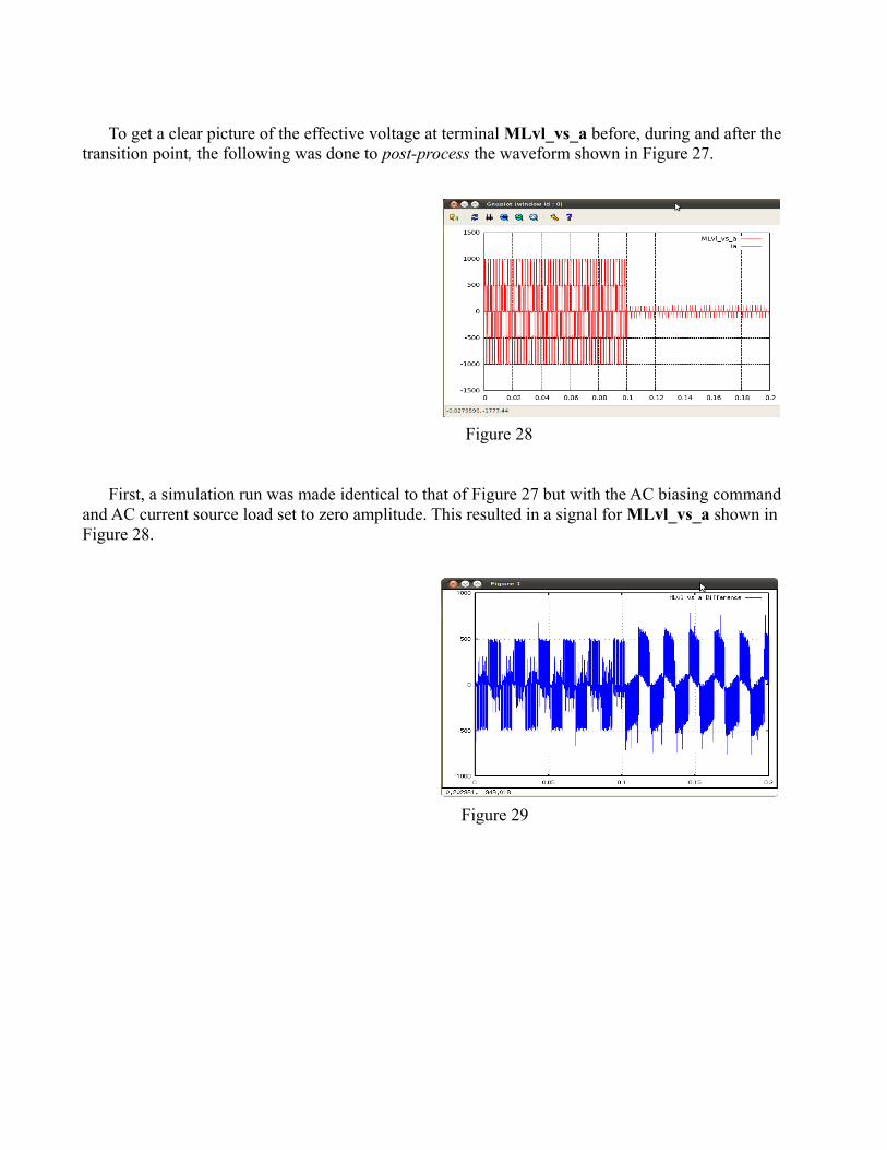
To get a clear picture of the effective voltage at terminal MLvl_vs_a before, during and after the transition point, the following was done to post-process the waveform shown in Figure 27.
Figure 28
First, a simulation run was made identical to that of Figure 27 but with the AC biasing command and AC current source load set to zero amplitude. This resulted in a signal for MLvl_vs_a shown in Figure 28.
Figure 29
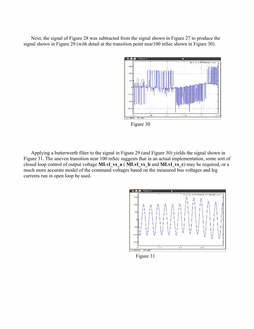
Next, the signal of Figure 28 was subtracted from the signal shown in Figure 27 to produce the signal shown in Figure 29 (with detail at the transition point near100 mSec shown in Figure 30).
Figure 30
Applying a butterworth filter to the signal in Figure 29 (and Figure 30) yields the signal shown in Figure 31. The uneven transition near 100 mSec suggests that in an actual implementation, some sort ofclosed loop control of output voltage MLvl_vs_a ( MLvl_vs_b and MLvl_vs_c) may be required, or a much more accurate model of the command voltages based on the measured bus voltages and leg currents run in open loop be used.
Figure 31
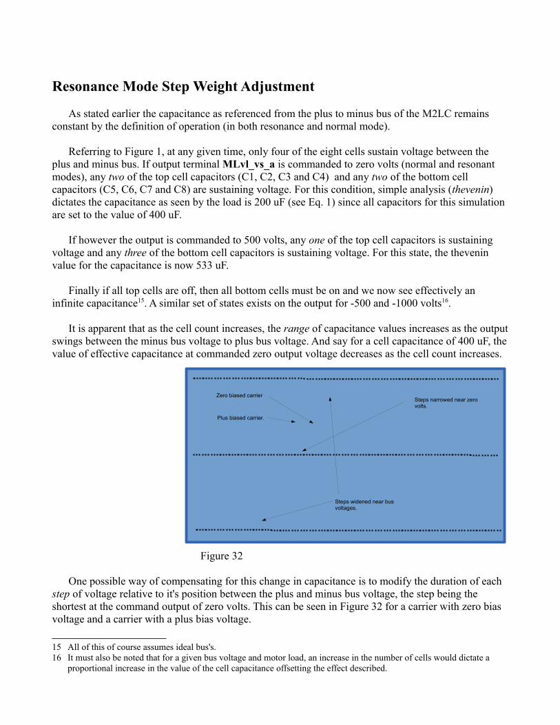
Resonance Mode Step Weight Adjustment
As stated earlier the capacitance as referenced from the plus to minus bus of the M2LC remains constant by the definition of operation (in both resonance and normal mode).
Referring to Figure 1, at any given time, only four of the eight cells sustain voltage between the plus and minus bus. If output terminal MLvl_vs_a is commanded to zero volts (normal and resonant modes), any two of the top cell capacitors (C1, C2, C3 and C4) and any two of the bottom cell capacitors (C5, C6, C7 and C8) are sustaining voltage. For this condition, simple analysis (thevenin) dictates the capacitance as seen by the load is 200 uF (see Eq. 1) since all capacitors for this simulation are set to the value of 400 uF.
If however the output is commanded to 500 volts, any one of the top cell capacitors is sustaining voltage and any three of the bottom cell capacitors is sustaining voltage. For this state, the thevenin value for the capacitance is now 533 uF.
Finally if all top cells are off, then all bottom cells must be on and we now see effectively an infinite capacitance15. A similar set of states exists on the output for -500 and -1000 volts16.
It is apparent that as the cell count increases, the range of capacitance values increases as the outputswings between the minus bus voltage to plus bus voltage. And say for a cell capacitance of 400 uF, thevalue of effective capacitance at commanded zero output voltage decreases as the cell count increases.
Figure 32
One possible way of compensating for this change in capacitance is to modify the duration of each step of voltage relative to it's position between the plus and minus bus voltage, the step being the shortest at the command output of zero volts. This can be seen in Figure 32 for a carrier with zero bias voltage and a carrier with a plus bias voltage.
15 All of this of course assumes ideal bus's. 16 It must also be noted that for a given bus voltage and motor load, an increase in the number of cells would dictate a
proportional increase in the value of the cell capacitance offsetting the effect described.
Steps narrowed near zerovolts.
Steps widened near busvoltages.
Zero biased carrier
Plus biased carrier.

Cell Balancing by Circulation or Selection
Cell circulation (or selection) involves the scheduling (or selection by the current value of capacitorvoltage) of eligible cells to be switched into the circuit during normal or resonant mode operation.
Cells in the top or bottom legs are selected based on the current switch state. For example, at a command output of zero on MLvl_vs_a (refer to Figure 1), there are two of four candidates on the cells of the top leg (C1 through C4) and two of four candidates on the cells of the bottom leg (C5 through C8) eligible for connection into the circuit. At +500 volts of (commanded), there are one of four cell capacitors eligible for the top and three of four eligible for the bottom.
All simulation plots presented above assign the value of 400 uF to cell capacitors C1 though C8. This along with the fact that the maximum simulation run for all demonstrations described above never exceeds 200 mSec. Under these circumstances, there is no real need for circulating or selecting active cells canidates in the top and bottom legs of the M2LC circuit.
However in real life, this is not the case since run times are indeterminate and cell characteristics such as the varying capacitor tolerances and switch losses are a factor.
Two approaches for scheduling are used. Cell circulation or cell selection. Circulation involves simply rotating the gating (IBGT) commands to each cell of a given leg at some predetermined rate. The first four sequences are shown in Figure 33.
Cmd_1 Cell 1 Cmd_2 Cell 1 Cmd_2 Cell 1 Cmd_3 Cell 1 Cmd_3 Cell 1Cmd_2 Cell 2 Cmd_3 Cell 2 Cmd_3 Cell 2 Cmd_4 Cell 2 Cmd_4 Cell 2Cmd_3 Cell 3 Cmd_4 Cell 3 Cmd_4 Cell 3 Cmd_1 Cell 3 Cmd_1 Cell 3Cmd_4 Cell 4 Cmd_1 Cell 4 Cmd_1 Cell 4 Cmd_2 Cell 4 Cmd_2 Cell 4Cmd_5 Cell 5 Cmd_5 Cell 5 Cmd_6 Cell 5 Cmd_6 Cell 5 Cmd_7 Cell 5Cmd_6 Cell 6 Cmd_6 Cell 6 Cmd_7 Cell 6 Cmd_7 Cell 6 Cmd_8 Cell 6Cmd_7 Cell 7 Cmd_7 Cell 7 Cmd_8 Cell 7 Cmd_8 Cell 7 Cmd_1 Cell 7Cmd_8 Cell 8 Cmd_8 Cell 8 Cmd_1 Cell 8 Cmd_1 Cell 8 Cmd_2 Cell 8
Figure 33
For our example of a 5-level converter, the sequence repeats every 8 sequences.
A patent for the circulation method described above is held by Curtiss-Wright Corporation. The method is simple to implement in logic and makes the assumption (a correct assumption) that balancingcan be achieved simply by rotation without the need for monitoring the cell voltage state.
A public domain approach used for re-balancing involves selecting eligible cells for insertion based on their current value of capacitor voltage and the direction of load current. This approach requires the monitoring of cell voltages. In current FPGA/DSP technology, this is not a problem since each cell would be smart in the sense that a high speed serial connection would connect each of the cells control modules to the central processing unit.
Up to this point, all simulations were run using the cell circulation method. The next section demonstrates the benefits of using the selection approach for cell re-balancing.
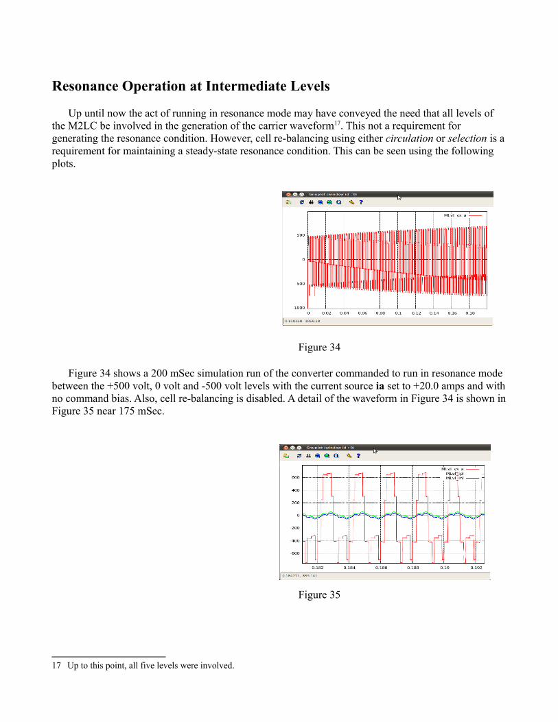
Resonance Operation at Intermediate Levels
Up until now the act of running in resonance mode may have conveyed the need that all levels of the M2LC be involved in the generation of the carrier waveform17. This not a requirement for generating the resonance condition. However, cell re-balancing using either circulation or selection is arequirement for maintaining a steady-state resonance condition. This can be seen using the following plots.
Figure 34
Figure 34 shows a 200 mSec simulation run of the converter commanded to run in resonance mode between the +500 volt, 0 volt and -500 volt levels with the current source ia set to +20.0 amps and withno command bias. Also, cell re-balancing is disabled. A detail of the waveform in Figure 34 is shown inFigure 35 near 175 mSec.
Figure 35
17 Up to this point, all five levels were involved.

This is in contrast to the waveforms shown in Figure 6 and Figure 9 above where resonance operation was performed between all five levels with cell re-balancing enabled (using the circulation method).
Note that in Figure 34 and Figure 35, the waveforms show indication of collapse, the zero level drops towards the minus bus and cell voltages become unbalanced.
Figure 36
Next, with command bias still set to zero, cell re-balancing is enabled this time using the cell selection method described above. The effects are shown in Figure 36 and 37.
Figure 37
As can be seen in these figures, the system has been stabilized and we are now able to sustain a DC
current at ia of +20.0 amps while running between the levels of -500, 0 and +500 volts.
Note in Figure 37 that by adding MLvl_ipl and MLvl_inl together, the result is an AC current center at zero. This indicates that we are drawing -10 amps from the lower leg and +10 amps from the upper leg to satisfy the value of 20.0 amps flowing at ia (See Figure 1).

Being that Mlvl_ipl and Mlvl_inl add together to create an AC current with no DC bias, than the current following in each cell capacitor should also have an average value of zero. Selecting an arbitrarily cell capacitor C2 (Figure 1), we see the current MLvl_i2 as shown in Figure 38
Figure 38
Under ideal conditions, the average current should be zero. Note the negative going turn-on current spikes in Figure 38. This is due to (in simulation), of the clearing of the forward conducting state in D21 by switch S22 in the simulator. This condition parallels (quite nicely I may add) to the actual clearing of charge (reverse recovery) of a diode in the forward state. The simulator is set to allow no more than 250 amps to flow when this condition occurs.
It can be seen that cell selection can be used as a method for stabilizing the system by attempting to distribute and maintain an equal amount of charge on the cell capacitors.
Two intermediate modulation methods can be employed. The first is similar to the modulation method discussed for Figures 21, 22 and 23 above operating at rail-to-rail. This is shown in Figure 39 and with more detail in Figure 40 near the area where modulation is applied.
Figure 39 Figure 40

Like the test for Figures 21, 22 and 23 the modulation shown in Figures 39 and 40 provides for a high degree of resolution. However, there may be issues with stability. In an actual design where the bus impedance is not zero and effected by the modulation of the other two phases the currents
MLvl_ipl and MLvl_inl may vary from cycle to cycle.
Figure 41 Figure 42
A second type of modulation now presents itself because we gain a degree of freedom (albeit limited) in where we place the zero level. This is shown in Figure 41 and with more detail in Figure 42 near the area where modulation is applied.
The method of modulation shown in Figures 41 and 42 provide for a more course control of the bias voltage. This would require the load inductance to be higher than that required for the first method.However, inter-phase current stability may be less of an issue for this approach.
In the context of operation in a three phase system, the first method of modulation is shown in Figure 43, the second shown in Figure 44
Figure 43 Figure 44
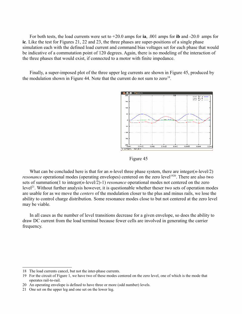
For both tests, the load currents were set to +20.0 amps for ia, .001 amps for ib and -20.0 amps for ic. Like the test for Figures 21, 22 and 23, the three phases are super-positions of a single phase simulation each with the defined load current and command bias voltages set for each phase that wouldbe indicative of a commutation point of 120 degrees. Again, there is no modeling of the interaction of the three phases that would exist, if connected to a motor with finite impedance.
Finally, a super-imposed plot of the three upper leg currents are shown in Figure 45, produced by the modulation shown in Figure 44. Note that the current do not sum to zero18.
Figure 45
What can be concluded here is that for an n-level three phase system, there are integer(n-level/2) resonance operational modes (operating envelopes) centered on the zero level1920. There are also two sets of summation(1 to integer(n-level/2)-1) resonance operational modes not centered on the zero level21. Without further analysis however, it is questionable whether theser two sets of operation modesare usable for as we move the centers of the modulation closer to the plus and minus rails, we lose the ability to control charge distribution. Some resonance modes close to but not centered at the zero level may be viable.
In all cases as the number of level transitions decrease for a given envelope, so does the ability to draw DC current from the load terminal because fewer cells are involved in generating the carrier frequency.
18 The load currents cancel, but not the inter-phase currents.19 For the circuit of Figure 1, we have two of these modes centered on the zero level, one of which is the mode that
operates rail-to-rail.20 An operating envelope is defined to have three or more (odd number) levels.21 One set on the upper leg and one set on the lower leg.

Appendix A - Simulator
The tool used to simulate the circuit shown in Figure 1 was generated by a simulation program written in C++. This simulator was originally designed as an ODE solver using a forth order Runge-Kutta interpolation algorithm run on each pass. In this same pass, a sixth order Runge-Kutta was run and difference in outputs between the forth and the sixth order algorithm was used to drive a variable time step algorithm.
Later, a SPICE solver was added to this C++ code. The signals shown in all plots shown above were generated by this SPICE solver. However, the original variable time step algorithm was not compatible with newly added SPICE module. As result, all generated waveforms shown in the main body of this document were executed in fixed time at an increment of .00000064 seconds. The reason, this specific value of time stepping was chosen will be made clear below.
In order to ensure the validity of this newly added SPICE module, the established open source NG-SPICE solver was used to compare results on a common test circuit. The test configuration for both the custom C++ solver and the NG-SPICE solver was the M2LC circuit shown in Figure 1 above with the output terminal MLvl_vs_a connected to a load circuit shown in Figure 46 below.
Figure 46
For both solvers, the M2LC was set to operate in normal mode with a low frequency reference command22. The results were then compared using two simulated output signals, the voltage at terminalMLvl_vs_a and the coupled current ib (see Figure 46) which is formed by the transformer coupling produced by element Lm.
22 The nodal circuit description for the test code run on the NG-SPICE solver is not included in this document.
MLvl_vs_a
ia
ibLm_b
Lm_a
Lb
La
Rb
Ra Ca
Cb
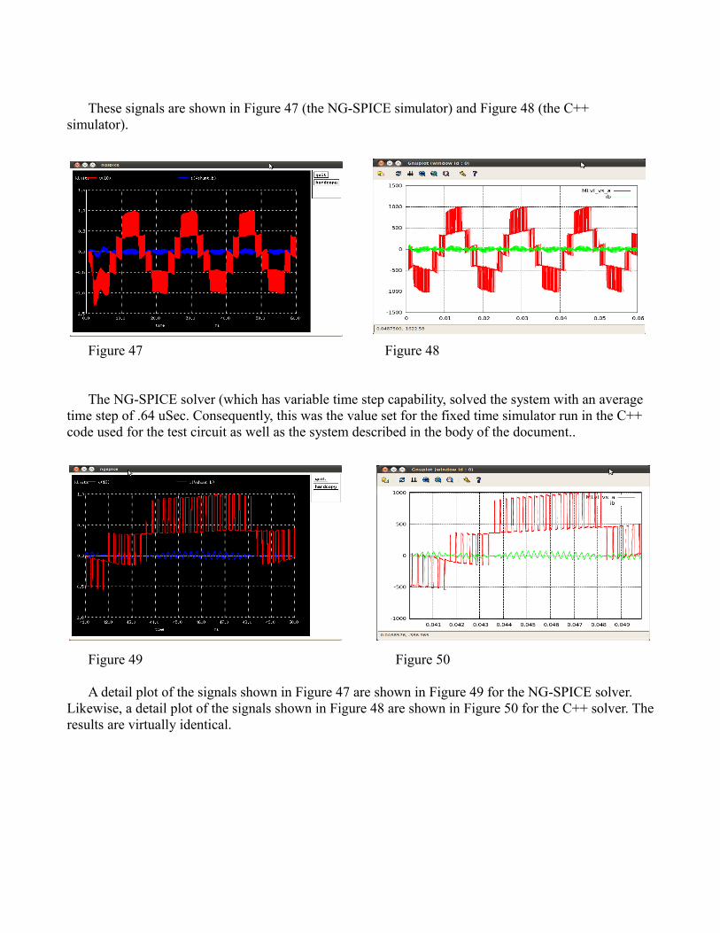
These signals are shown in Figure 47 (the NG-SPICE simulator) and Figure 48 (the C++ simulator).
Figure 47 Figure 48
The NG-SPICE solver (which has variable time step capability, solved the system with an average time step of .64 uSec. Consequently, this was the value set for the fixed time simulator run in the C++ code used for the test circuit as well as the system described in the body of the document..
Figure 49 Figure 50
A detail plot of the signals shown in Figure 47 are shown in Figure 49 for the NG-SPICE solver. Likewise, a detail plot of the signals shown in Figure 48 are shown in Figure 50 for the C++ solver. Theresults are virtually identical.

Acknowledgment
The basis for this paper was provided by the paper:
A new modular voltage source inverter topology
A. Lesnicar, R. Marquardt
INSTITUTE OF POWER ELECTRONICS AND CONTROLUniversität der Bundeswehr München
Provisional Patent Application
The information provided in this document is currently held as a provisional patent. However, in alllikelihood, I will probably let this submittal expire. If there is any interest in using some or all of these ideas in a design, please contact me at mailto:[email protected] .
Provisional Patent Application Number: 61/996,366Filing Date: 05/06/2014
NOTE: As of Revision C of this document (12/27/14), all information contained in this document is part of the public domain .