operation manual - omron on trascon...
TRANSCRIPT
Cat.No. W345–E1–2
Analog I/O Units
SYSMAC CS1 SeriesCS1W-AD041/081CS1W-DA041/08V/08CCS1W-MAD44
OPERATION MANUAL

SYSMAC CS1 SeriesCS1W-AD041/081 CS1W-DA041/08V/08C CS1W-MAD44 Analog I/O UnitsOperation Manual
Revised August 1999

!
!
!
v
Notice:OMRON products are manufactured for use according to proper procedures by a qualified operatorand only for the purposes described in this manual.
The following conventions are used to indicate and classify precautions in this manual. Always heedthe information provided with them. Failure to heed precautions can result in injury to people or dam-age to property.
DANGER Indicates an imminently hazardous situation which, if not avoided, will result in death orserious injury.
WARNING Indicates a potentially hazardous situation which, if not avoided, could result in death orserious injury.
Caution Indicates a potentially hazardous situation which, if not avoided, may result in minor ormoderate injury, or property damage.
OMRON Product ReferencesAll OMRON products are capitalized in this manual. The word “Unit” is also capitalized when it refersto an OMRON product, regardless of whether or not it appears in the proper name of the product.
The abbreviation “Ch,” which appears in some displays and on some OMRON products, often means“word” and is abbreviated “Wd” in documentation in this sense.
The abbreviation “PC” means Programmable Controller and is not used as an abbreviation for any-thing else.
Visual AidsThe following headings appear in the left column of the manual to help you locate different types ofinformation.
Note Indicates information of particular interest for efficient and convenient operationof the product.
1, 2, 3... 1. Indicates lists of one sort or another, such as procedures, checklists, etc.
OMRON, 1999All rights reserved. No part of this publication may be reproduced, stored in a retrieval system, or transmitted, in anyform, or by any means, mechanical, electronic, photocopying, recording, or otherwise, without the prior written permis-sion of OMRON.
No patent liability is assumed with respect to the use of the information contained herein. Moreover, because OMRON isconstantly striving to improve its high-quality products, the information contained in this manual is subject to changewithout notice. Every precaution has been taken in the preparation of this manual. Nevertheless, OMRON assumes noresponsibility for errors or omissions. Neither is any liability assumed for damages resulting from the use of the informa-tion contained in this publication.
TABLE OF CONTENTS
vii
PRECAUTIONS xi. . . . . . . . . . . . . . . . . . . . . . . . . . . . . . . . . 1 Intended Audience xii. . . . . . . . . . . . . . . . . . . . . . . . . . . . . . . . . . . . . . . . . . . . . . . . . . . . . . . . . . . 2 General Precautions xii. . . . . . . . . . . . . . . . . . . . . . . . . . . . . . . . . . . . . . . . . . . . . . . . . . . . . . . . . . 3 Safety Precautions xii. . . . . . . . . . . . . . . . . . . . . . . . . . . . . . . . . . . . . . . . . . . . . . . . . . . . . . . . . . . 4 Operating Environment Precautions xiii. . . . . . . . . . . . . . . . . . . . . . . . . . . . . . . . . . . . . . . . . . . . . 5 Application Precautions xiii. . . . . . . . . . . . . . . . . . . . . . . . . . . . . . . . . . . . . . . . . . . . . . . . . . . . . . 6 EC Directives xv. . . . . . . . . . . . . . . . . . . . . . . . . . . . . . . . . . . . . . . . . . . . . . . . . . . . . . . . . . . . . . 7 Other Applicable Directives xv. . . . . . . . . . . . . . . . . . . . . . . . . . . . . . . . . . . . . . . . . . . . . . . . . . . 8 Precautions for the C200H-AD003, C200H-DA003/004 and C200H-MAD01 xv. . . . . . . . . . . .
SECTION 1System Design 1. . . . . . . . . . . . . . . . . . . . . . . . . . . . . . . . . . .
1-1 Features and Functions 2. . . . . . . . . . . . . . . . . . . . . . . . . . . . . . . . . . . . . . . . . . . . . . . . . . . . 1-2 Basic Configuration 5. . . . . . . . . . . . . . . . . . . . . . . . . . . . . . . . . . . . . . . . . . . . . . . . . . . . . . 1-3 Function Applications 7. . . . . . . . . . . . . . . . . . . . . . . . . . . . . . . . . . . . . . . . . . . . . . . . . . . .
SECTION 2Analog Input Units 9. . . . . . . . . . . . . . . . . . . . . . . . . . . . . . .
2-1 Specifications 10. . . . . . . . . . . . . . . . . . . . . . . . . . . . . . . . . . . . . . . . . . . . . . . . . . . . . . . . . . . 2-2 Operating Procedure 15. . . . . . . . . . . . . . . . . . . . . . . . . . . . . . . . . . . . . . . . . . . . . . . . . . . . . . 2-3 Components and Switch Settings 21. . . . . . . . . . . . . . . . . . . . . . . . . . . . . . . . . . . . . . . . . . . . 2-4 Wiring 24. . . . . . . . . . . . . . . . . . . . . . . . . . . . . . . . . . . . . . . . . . . . . . . . . . . . . . . . . . . . . . . . . 2-5 Exchanging Data with the CPU Unit 28. . . . . . . . . . . . . . . . . . . . . . . . . . . . . . . . . . . . . . . . . 2-6 Analog Input Functions and Operating Procedures 35. . . . . . . . . . . . . . . . . . . . . . . . . . . . . . 2-7 Adjusting Offset and Gain 41. . . . . . . . . . . . . . . . . . . . . . . . . . . . . . . . . . . . . . . . . . . . . . . . . 2-8 Handling Errors and Alarms 49. . . . . . . . . . . . . . . . . . . . . . . . . . . . . . . . . . . . . . . . . . . . . . .
SECTION 3Analog Output Units 55. . . . . . . . . . . . . . . . . . . . . . . . . . . . .
3-1 Specifications 56. . . . . . . . . . . . . . . . . . . . . . . . . . . . . . . . . . . . . . . . . . . . . . . . . . . . . . . . . . . 3-2 Operating Procedure 60. . . . . . . . . . . . . . . . . . . . . . . . . . . . . . . . . . . . . . . . . . . . . . . . . . . . . . 3-3 Components and Switch Settings 66. . . . . . . . . . . . . . . . . . . . . . . . . . . . . . . . . . . . . . . . . . . . 3-4 Wiring 69. . . . . . . . . . . . . . . . . . . . . . . . . . . . . . . . . . . . . . . . . . . . . . . . . . . . . . . . . . . . . . . . . 3-5 Exchanging Data with the CPU Unit 72. . . . . . . . . . . . . . . . . . . . . . . . . . . . . . . . . . . . . . . . . 3-6 Analog Output Functions and Operating Procedures 79. . . . . . . . . . . . . . . . . . . . . . . . . . . . 3-7 Adjusting Offset and Gain 84. . . . . . . . . . . . . . . . . . . . . . . . . . . . . . . . . . . . . . . . . . . . . . . . . 3-8 Handling Errors and Alarms 94. . . . . . . . . . . . . . . . . . . . . . . . . . . . . . . . . . . . . . . . . . . . . . .
SECTION 4Analog I/O Unit 99. . . . . . . . . . . . . . . . . . . . . . . . . . . . . . . . .
4-1 Specifications 100. . . . . . . . . . . . . . . . . . . . . . . . . . . . . . . . . . . . . . . . . . . . . . . . . . . . . . . . . . . 4-2 Operating Procedure 107. . . . . . . . . . . . . . . . . . . . . . . . . . . . . . . . . . . . . . . . . . . . . . . . . . . . . . 4-3 Components and Switch Settings 114. . . . . . . . . . . . . . . . . . . . . . . . . . . . . . . . . . . . . . . . . . . . 4-4 Wiring 117. . . . . . . . . . . . . . . . . . . . . . . . . . . . . . . . . . . . . . . . . . . . . . . . . . . . . . . . . . . . . . . . . 4-5 Exchanging Data with the CPU Unit 121. . . . . . . . . . . . . . . . . . . . . . . . . . . . . . . . . . . . . . . . . 4-6 Analog Input Functions and Operating Procedures 129. . . . . . . . . . . . . . . . . . . . . . . . . . . . . . 4-7 Analog Output Functions and Operating Procedures 135. . . . . . . . . . . . . . . . . . . . . . . . . . . . 4-8 Ratio Conversion Function 138. . . . . . . . . . . . . . . . . . . . . . . . . . . . . . . . . . . . . . . . . . . . . . . . 4-9 Adjusting Offset and Gain 141. . . . . . . . . . . . . . . . . . . . . . . . . . . . . . . . . . . . . . . . . . . . . . . . . 4-10 Handling Errors and Alarms 156. . . . . . . . . . . . . . . . . . . . . . . . . . . . . . . . . . . . . . . . . . . . . . .
AppendicesA Dimensions 163. . . . . . . . . . . . . . . . . . . . . . . . . . . . . . . . . . . . . . . . . . . . . . . . . . . . . . . . . . . . . . . . B Sample Programs 165. . . . . . . . . . . . . . . . . . . . . . . . . . . . . . . . . . . . . . . . . . . . . . . . . . . . . . . . . . . C Data Memory Coding Sheets 174. . . . . . . . . . . . . . . . . . . . . . . . . . . . . . . . . . . . . . . . . . . . . . . . . .

TABLE OF CONTENTS
viii
Index 185. . . . . . . . . . . . . . . . . . . . . . . . . . . . . . . . . . . . . . . . . . Revision History 191. . . . . . . . . . . . . . . . . . . . . . . . . . . . . . . . .

ix
About this Manual:
This manual describes the installation and operation of the CS1W-AD041/081 Analog Input Units, theCS1W-DA041/08V/08C Analog Output Units, and the CS1W-MAD44 Analog I/O Unit, and includes thesections described below.
The input function of CS1-series Analog I/O Units converts analog sensor output to the digital format andtransmits it to CS1-series PCs. The output function converts digital data from the PC to the analog formatfor output.
Please read this manual and the other manuals related to the CS1-series Analog I/O Units carefully andbe sure you understand the information provided before attempting to install and operate the Units.
There are five manuals used with the CS1-series Analog I/O Units. These manuals are listed in the follow-ing table. The suffixes have been omitted from the catalog numbers. Be sure you are using the mostrecent version for your area.
Name Cat. No. Contents
SYSMAC CS1-seriesCS1G/H-CPU-E Programmable ControllersOperation Manual
W339-E1-1 Describes the installation and operation of the CS1-series PCs.
SYSMAC CS1-seriesCS1G/H-CPU-E Programmable ControllersProgramming Manual
W340-E1-1 Describes the ladder diagram programming instructionssupported by CS1-series PCs.
SYSMAC CS1-series C200H-PRO27-E, CQM1-PRO01-EProgramming Consoles Operation Manual
W341-E-1 Provides information on how to program and operateCS1-series PCs using a Programming Console.
SYSMAC CS1-series CS1G/H-CPU-E,CS1W-SCB21/41, CS1W-SCU21Communications CommandsReference Manual
W342-E1-1 Describes the C-series (Host Link) and FINS communicationscommands used with CS1-series PCs.
SYSMAC WS02-CXP-ECX-Programmer Operation Manual
--- Provides information on how to use the CX-Programmer, aprogramming device that supports the CS1-series PCs.
Section 1 describes the features and system configurations of CS1W-AD041/081 Analog Input Units,CS1W-DA041/08V/08C Analog Output Units, and CS1W-MAD44 Analog I/O Unit.
Section 2 explains how to use the CS1W-AD041/081 Analog Input Units.
Section 3 explains how to use the CS1W-DA041/08V/08C Analog Output Units.
Section 4 explains how to use the CS1W-MAD44 Analog I/O Unit.
Appendix A provides details on dimensions.
Appendix B gives programming examples.
Appendix C provides data memory coding sheets.
WARNING Failure to read and understand the information provided in this manual may result inpersonal injury or death, damage to the product, or product failure. Please read eachsection in its entirety and be sure you understand the information provided in the sectionand related sections before attempting any of the procedures or operations given.
!

xi
PRECAUTIONS
This section provides general precautions for using the Programmable Controller (PC) and Analog I/O Units.
The information contained in this section is important for the safe and reliable application of the Analog I/O Unit. Youmust read this section and understand the information contained before attempting to set up or operate a PC systemand Analog I/O Unit.
1 Intended Audience xii. . . . . . . . . . . . . . . . . . . . . . . . . . . . . . . . . . . . . . . . . . . . . . . . . . . . . . . . . . . . 2 General Precautions xii. . . . . . . . . . . . . . . . . . . . . . . . . . . . . . . . . . . . . . . . . . . . . . . . . . . . . . . . . . . 3 Safety Precautions xii. . . . . . . . . . . . . . . . . . . . . . . . . . . . . . . . . . . . . . . . . . . . . . . . . . . . . . . . . . . . 4 Operating Environment Precautions xiii. . . . . . . . . . . . . . . . . . . . . . . . . . . . . . . . . . . . . . . . . . . . . . 5 Application Precautions xiii. . . . . . . . . . . . . . . . . . . . . . . . . . . . . . . . . . . . . . . . . . . . . . . . . . . . . . . . 6 EC Directives xv. . . . . . . . . . . . . . . . . . . . . . . . . . . . . . . . . . . . . . . . . . . . . . . . . . . . . . . . . . . . . . . . 7 Other Applicable Directives xv. . . . . . . . . . . . . . . . . . . . . . . . . . . . . . . . . . . . . . . . . . . . . . . . . . . . 8 Precautions for the C200H-AD003, C200H-DA003/004 and C200H-MAD01 xv. . . . . . . . . . . . .

!
!
!
!
8Safety Precautions
xii
1 Intended AudienceThis manual is intended for the following personnel, who must also have knowl-edge of electrical systems (an electrical engineer or the equivalent).
• Personnel in charge of installing FA systems
• Personnel in charge of designing FA systems
• Personnel in charge of managing FA systems and facilities
2 General PrecautionsThe user must operate the product according to the performance specificationsdescribed in the operation manuals.
Before using the product under conditions which are not described in the manualor applying the product to nuclear control systems, railroad systems, aviationsystems, vehicles, combustion systems, medical equipment, amusementmachines, safety equipment, and other systems, machines, and equipment thatmay have a serious influence on lives and property if used improperly, consultyour OMRON representative.
Make sure that the ratings and performance characteristics of the product aresufficient for the systems, machines, and equipment, and be sure to provide thesystems, machines, and equipment with double safety mechanisms.
This manual provides information for programming and operating OMRON Ana-log I/O Units. Be sure to read this manual before attempting to use the softwareand keep this manual close at hand for reference during operation.
WARNING It is extremely important that a PC and all PC Units be used for the specifiedpurpose and under the specified conditions, especially in applications that candirectly or indirectly affect human life. You must consult with your OMRONrepresentative before applying a PC System to the above-mentionedapplications.
3 Safety Precautions
WARNING Do not attempt to take any Unit apart while power is being supplied. Doing somay result in electric shock.
WARNING Do not touch any of the terminals or terminal blocks while power is beingsupplied. Doing so may result in electric shock.
WARNING Provide safety measures in external circuits (i.e., not in the ProgrammableController), including the following items, in order to ensure safety in the systemif an abnormality occurs due to malfunction of the PC or another external factoraffecting the PC operation. Not doing so may result in serious accidents.
• Emergency stop circuits, interlock circuits, limit circuits, and similar safetymeasures must be provided in external control circuits.
• The PC will turn OFF all outputs when its self-diagnosis function detects anyerror or when a severe failure alarm (FALS) instruction is executed. As a coun-termeasure for such errors, external safety measures must be provided toensure safety in the system.
• The PC outputs may remain ON or OFF due to deposition or burning of theoutput relays or destruction of the output transistors. As a countermeasure forsuch problems, external safety measures must be provided to ensure safety inthe system.

!
!
!
!
!
!
5Application Precautions
xiii
Caution Tighten the screws on the terminal block of the AC Power Supply Unit to thetorque specified in the operation manual. The loose screws may result in burningor malfunction.
Caution Execute online edit only after confirming that no adverse effects will be causedby extending the cycle time. Otherwise, the input signals may not be readable.
4 Operating Environment Precautions
Caution Do not operate the control system in the following places:
• Locations subject to direct sunlight.
• Locations subject to temperatures or humidity outside the range specified inthe specifications.
• Locations subject to condensation as the result of severe changes in tempera-ture.
• Locations subject to corrosive or flammable gases.
• Locations subject to dust (especially iron dust) or salts.
• Locations subject to exposure to water, oil, or chemicals.
• Locations subject to shock or vibration.
Caution Take appropriate and sufficient countermeasures when installing systems in thefollowing locations:
• Locations subject to static electricity or other forms of noise.
• Locations subject to strong electromagnetic fields.
• Locations subject to possible exposure to radioactivity.
• Locations close to power supplies.
Caution The operating environment of the PC System can have a large effect on the lon-gevity and reliability of the system. Improper operating environments can lead tomalfunction, failure, and other unforeseeable problems with the PC System. Besure that the operating environment is within the specified conditions at installa-tion and remains within the specified conditions during the life of the system.
5 Application PrecautionsObserve the following precautions when using the PC.
WARNING Always heed these precautions. Failure to abide by the following precautionscould lead to serious or possibly fatal injury.
• Always connect to a class-3 ground (to 100 Ω or less) when installing the Units.Not connecting to a class-3 ground may result in electric shock.
• Always turn off the power supply to the PC before attempting any of the follow-ing. Not turning off the power supply may result in malfunction or electricshock.
• Mounting or dismounting I/O Units, CPU Units, Memory Cassettes, or anyother Units.
• Assembling the Units.
• Setting DIP switch or rotary switches.
• Connecting or wiring the cables.
• Connecting or disconnecting the connectors.
!
5Application Precautions
xiv
Caution Failure to abide by the following precautions could lead to faulty operation of thePC or the system, or could damage the PC or PC Units. Always heed these pre-cautions.
• Fail-safe measures must be taken by the customer to ensure safety in theevent of incorrect, missing, or abnormal signals caused by broken signal lines,momentary power interruptions, or other causes.
• Always use the power supply voltage specified in this manual. An incorrectvoltage may result in malfunction or burning.
• Take appropriate measures to ensure that the specified power with the ratedvoltage and frequency is supplied. Be particularly careful in places where thepower supply is unstable. An incorrect power supply may result in malfunction.
• Install external breakers and take other safety measures against short-circuit-ing in external wiring. Insufficient safety measures against short-circuiting mayresult in burning.
• Do not apply voltages to input sections in excess of the rated input voltage.Excess voltages may result in burning.
• Do not apply voltages or connect loads in excess of the maximum switchingcapacity to output sections. Excess voltage or loads may result in burning.
• Turn OFF the power to the PC before performing the following operations.
• Mounting or removing the Analog I/O Unit, the CPU Unit, or the MemoryPack.
• Assembling Racks.
• Setting the DIP switch or rotary switch.
• Performing wiring or connecting cables.
• Be sure that all the mounting screws, terminal screws, and cable connectorscrews are tightened to the torque specified in the relevant manuals. Incorrecttightening torque may result in malfunction.
• Do not attempt to disassemble, repair, or modify any Units.
• Be sure to confirm that the DIP switch and the data memory (DM) are properlyset.
• Leave the label attached to the Unit when wiring. Removing the label mayresult in malfunction.
• Remove the labels after the completion of wiring to ensure proper heat dissipa-tion. Leaving the label attached may result in malfunction.
• Mount the Unit only after checking the terminal block completely.
• Be sure that the terminal blocks, Memory Units, expansion cables, and otheritems with locking devices are properly locked into place. Improper lockingmay result in malfunction.
• Check the user program for proper execution before actually running it on theUnit. Not checking the program may result in an unexpected operation.
• Use crimp terminals for wiring. Do not connect bare stranded wires directly toterminals. Connection of bare stranded wires may result in burning.
• Double-check all the wiring before turning on the power supply. Incorrect wir-ing may result in burning.
• Confirm that no adverse effect will occur in the system before attempting any ofthe following. Not doing so may result in an unexpected operation.
• Changing the operating mode of the PC.
• Force-setting/force-resetting any bit in memory.
• Changing the present value of any word or any set value in memory.

8Precautions for the C200H-AD003, C200H-DA003/004 and C200H-MAD01
xv
6 EC DirectivesCS1-series Units conform to EC Directives. For the system to conform to ECDirectives, however, the following precautions must be adhered to.
• CS1-series Units must be installed within control panels.
• Use reinforced insulation or double insulation for the DC power supplies usedfor the I/O power supplies.
• CS1-series Units that meet EC Directives also meet the Common EmissionStandard (EN50081-2). The measure necessary to ensure that standards,such as the radiated emission standard (10 m), are met, however, will varydepending on the overall configuration of the control panel, the other devicesconnected to the control panel, and wiring. You must therefore confirm that ECDirectives are met for the overall machine or device.
7 Other Applicable DirectivesApplicable Directives
• EMC Directive
• Low Voltage Directive
EMC and Low Voltage DirectivesEMC DirectiveIn order that OMRON products can be used with any machinery and in combina-tion with other manufacturer’s equipment, the products themselves aredesigned to comply with EMC standards (see note 1.), so that the assembledmachinery or device can then also easily comply with EMC standards.Even if machinery and equipment complies with EMC standards before assem-bly, this compliance may change depending on the device, the configuration ofthe control panel, and wiring, so OMRON cannot guarantee that particular sys-tem complies with the directive. You must therefore confirm that EMC Directivesare met for the overall machine or device.
Note EMC: One directive relating to Electro-Magnetic CompatibilityEMS: Electro-Magnetic Susceptibility standard EN61131-2EMI: Electro-Magnetic Interference standard EN50081-2Common Emission Standard EN50081-2, radiated emission standard (10 m)
Low Voltage DirectiveThe Low Voltage Directive provides that necessary safety standards are guar-anteed for devices operating at voltages of 50 to 1,000 VAC or 75 to 1,500 VDC.
8 Precautions for the C200H-AD003, C200H-DA003/004 andC200H-MAD01
Note the following important differences between the CS1W-series Analog I/OUnits and the C200H Analog I/O Units.
Current Input WiringThe CS1W-AD041/081 Analog Input Units and the CS1W-MAD44 Analog I/OUnit do not have a current input terminal. To switch analog conversion input fromvoltage input to current input, the voltage/current switch must be turned ON.Refer to 2-3-4 or 4-3-4 Voltage Current Switch.
Mean Value ProcessingThe default setting for mean value processing in the CS1W-AD041/081 AnalogInput Units and the CS1W-MAD44 Analog I/O Unit is mean value processingwith 2 buffers. By changing the setting in data memory, no mean processing canbe selected. Refer to 2-6-2 or 4-6-2 Mean Value Processing.

8Precautions for the C200H-AD003, C200H-DA003/004 and C200H-MAD01
xvi
Operation Mode SwitchTo change from normal mode to adjustment mode, or vice versa, with theC200H-AD003, C200H-DA003/004, or C200H-MAD01 Analog I/O Units, it isnecessary to create an I/O table. With the CS1W-series Analog I/O Units, theoperation mode switch can be used to make this change. Therefore the I/O tableis no longer necessary. Refer to 2-7-1, 3-7-1 or 4-9-1 Adjustment Mode Opera-tional Flow.
Error FlagsThe C200H-AD003, C200H-DA003/004, and C200H-MAD01 use error codes,whereas the CS1W-series Analog I/O Units use error flags. When the ERC indi-cator is lit due to a setting error in the DM area or an operating error, a bit flag willbe stored in the CIO Area. Refer to 2-8-2 Alarms Occurring at the Analog Input
Unit, 3-8-2 Alarms Occurring at the Analog Output Unit, or 4-10-2 Alarms Occur-ring at the Analog I/O Unit.

1
SECTION 1System Design
This section describes the features and system configurations of CS1W-AD041/081 Analog Input Units,CS1W-DA041/08V/08C Analog Output Units, and CS1W-MAD44 Analog I/O Units.
1-1 Features and Functions 2. . . . . . . . . . . . . . . . . . . . . . . . . . . . . . . . . . . . . . . . . . . . . . . . . . . . . 1-2 Basic Configuration 5. . . . . . . . . . . . . . . . . . . . . . . . . . . . . . . . . . . . . . . . . . . . . . . . . . . . . . .
1-2-1 Mounting Procedure 6. . . . . . . . . . . . . . . . . . . . . . . . . . . . . . . . . . . . . . . . . . . . . . . 1-2-2 Precautions 6. . . . . . . . . . . . . . . . . . . . . . . . . . . . . . . . . . . . . . . . . . . . . . . . . . . . . . .
1-3 Function Applications 7. . . . . . . . . . . . . . . . . . . . . . . . . . . . . . . . . . . . . . . . . . . . . . . . . . . . .
1-1SectionFeatures and Functions
2
1-1 Features and Functions
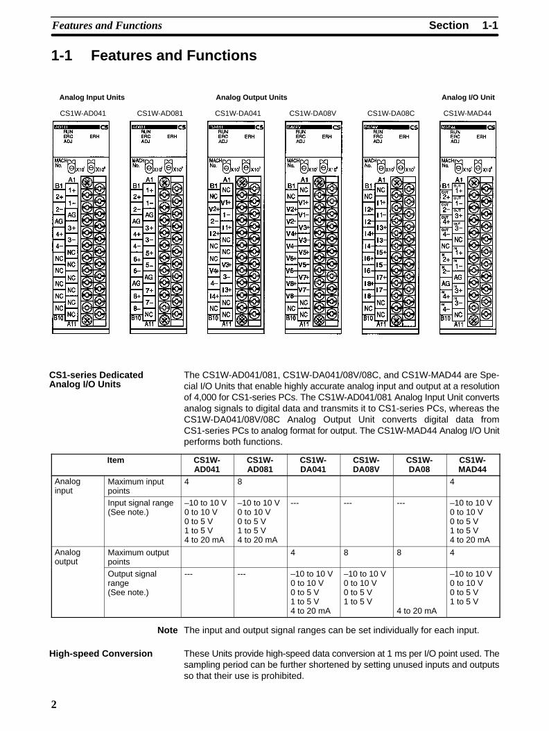
CS1W-MAD44
Analog I/O UnitAnalog Input Units Analog Output Units
CS1W-AD041 CS1W-AD081 CS1W-DA041 CS1W-DA08V CS1W-DA08C
The CS1W-AD041/081, CS1W-DA041/08V/08C, and CS1W-MAD44 are Spe-cial I/O Units that enable highly accurate analog input and output at a resolutionof 4,000 for CS1-series PCs. The CS1W-AD041/081 Analog Input Unit convertsanalog signals to digital data and transmits it to CS1-series PCs, whereas theCS1W-DA041/08V/08C Analog Output Unit converts digital data fromCS1-series PCs to analog format for output. The CS1W-MAD44 Analog I/O Unitperforms both functions.
Item CS1W-AD041
CS1W-AD081
CS1W-DA041
CS1W-DA08V
CS1W-DA08
CS1W-MAD44
Analoginput
Maximum inputpoints
4 8 4
Input signal range(See note.)
–10 to 10 V0 to 10 V0 to 5 V1 to 5 V4 to 20 mA
–10 to 10 V0 to 10 V0 to 5 V1 to 5 V4 to 20 mA
--- --- --- –10 to 10 V0 to 10 V0 to 5 V1 to 5 V4 to 20 mA
Analogoutput
Maximum outputpoints
4 8 8 4
Output signalrange(See note.)
--- --- –10 to 10 V0 to 10 V0 to 5 V1 to 5 V4 to 20 mA
–10 to 10 V0 to 10 V0 to 5 V1 to 5 V
4 to 20 mA
–10 to 10 V0 to 10 V0 to 5 V1 to 5 V
Note The input and output signal ranges can be set individually for each input.
These Units provide high-speed data conversion at 1 ms per I/O point used. Thesampling period can be further shortened by setting unused inputs and outputsso that their use is prohibited.
CS1-series DedicatedAnalog I/O Units
High-speed Conversion

1-1SectionFeatures and Functions
3
The input disconnection detection function can be used for analog inputs withinan input signal range of 1 to 5 V (4 to 20 mA). When this function is set for use,any input under 0.3 V will be regarded as a disconnection. For details, refer to2-4-3, 2-6-4, or 4-6-4 Input Disconnection Detection Function.
Analog I/O Unit CPU Unit
DisconnectionDetection Flag
The peak value hold function holds the maximum digital conversion value forevery input (including mean value processing). This function can be used withanalog input. The following diagram shows how digital conversion values areaffected when the peak value hold function is used. For details, refer to 2-6-3 or4-6-3 Peak Value Hold Function.
Peak hold bit
The output hold function can be used to hold the analog output value at any pre-set value when there is a fatal error at the CPU Unit or when specified by the CPUUnit. When output is stopped, CLR, HOLD, or MAX can be selected for output.For details, refer to 3-6-3 or 4-7-2 Output Hold Function.
Analog I/O Unit CPU Unit
Output EnableFlag OFF
CLR/HOLD/MAX
Input DisconnectionDetection Function
Peak Value HoldFunction
Output Hold Function

1-1SectionFeatures and Functions
4
The mean value function can be used to remove erroneous values that occurdue to factors such as noise that is included in analog inputs. The operatingmean is taken without affecting the data refresh cycle. For details, refer to 2-6-2or 4-6-2 Mean Value Processing.
Analog I/O Unit CPU Unit
Mean valueof “n” his-tory buffers
The CS1W-MAD44 Analog I/O Unit can output in analog format the results ofanalog inputs calculated for ratio and bias. For details, refer to 4-8 Ratio Conver-sion Function.
A x + B
Ratio and bias setting device
Ratio and bias
The A/D and D/A converter offset deviation and gain deviation can be adjustedfor each input and output. The offset and gain adjustments are made with theUnit set for the adjustment mode, and the adjustment values are stored in theUnit’s built-in EEPROM. For details, refer to 2-7, 3-7 or 4-9 Adjusting Offset andGain.
Analog Input Function
(Input signal range: 0 to 10 V)
Analog Output Function
(Output signal range: 0 to 10 V)
Gainadjustment
Gainadjustment
Analog input10 V
Offset adjustment Offset adjustment
Analogoutput
10 V
Adjustable range Adjustable range
Mean Value Function
Ratio ConversionFunction
Offset and GainAdjustment Function

1-2SectionBasic Configuration
5
1-2 Basic Configuration
Analog I/O Unit CPU Unit
Preamp
Transducer
Variable speedcontroller
Servo-controller
TemperaturePressureSpeedFlow rate
VoltageCurrentPowerPower factor
Regulator(Temperature control)
(Speed control)
(Position control)
Chart recorder
Sensor
Sensor
Note The above diagram is an installation example for the CS1W-AD081 AnalogInput Unit and CS1W-DA08V Analog Output Unit.
The CS1W-MAD44 Analog I/O Unit is a Special I/O Unit of the CS1 Series.
CS1W-MAD44 Analog I/O Units can be mounted to either CS1 CPU Racks orCS1 Expansion Racks. These Analog I/O Units cannot be mounted to C200HExpansion I/O Racks or SYSMAC BUS Slave Racks.
The number of Analog I/O Units that can be mounted to one Rack (i.e., a CPURack or Expansion Rack) depends on the maximum supply current of the PowerSupply Unit and the current consumption of other Units. If a Rack is to bemounted with Analog Input, Output, or I/O Units only, the following restrictionswill apply.
Power Supply Unit CS1W-AD041/081 CS1W-DA041/08V CS1W-MAD44 CS1W-DA8C
C200HW-PA204C200HW-PA204SC200HW-PA204RC200HW-PD204
6 3 3 2
C200HW-PA209R 10 7 6 5
Note The I/O bits of the Special I/O Unit are allocated according to the setting of theunit number switch on the front panel of the Unit, and not the slot number wherethe Unit is mounted.
Mounting Restrictions

1-2SectionBasic Configuration
6
1-2-1 Mounting ProcedureUse the following procedure to mount Analog I/O Units to the Backplane.
1, 2, 3... 1. Lock the top of the Analog I/O Unit into the slot on the Backplane and rotatethe Unit downwards as shown in the following diagram.
Hook
Backplane
2. While making sure to align the Unit properly with the connectors, tighten themounting screws securely to the tightening torque of 0.4 N m.
3. To remove the Unit, first loosen the mounting screws using a Phillips screw-driver.
Mounting screw
Leave enough space below each Rack, as shown in the following diagram formounting and removing the Units.
20 mm min.
20 mm min.
Backplane
Phillips screwdriver
1-2-2 PrecautionsBe sure to turn OFF the power supply to the PC before installing or disconnect-ing Units or connecting lines.To reduce the risk of malfunctioning due to electrical noise, wire input and outputlines in separate ducts from high-voltage and power lines.
1-3SectionFunction Applications
7
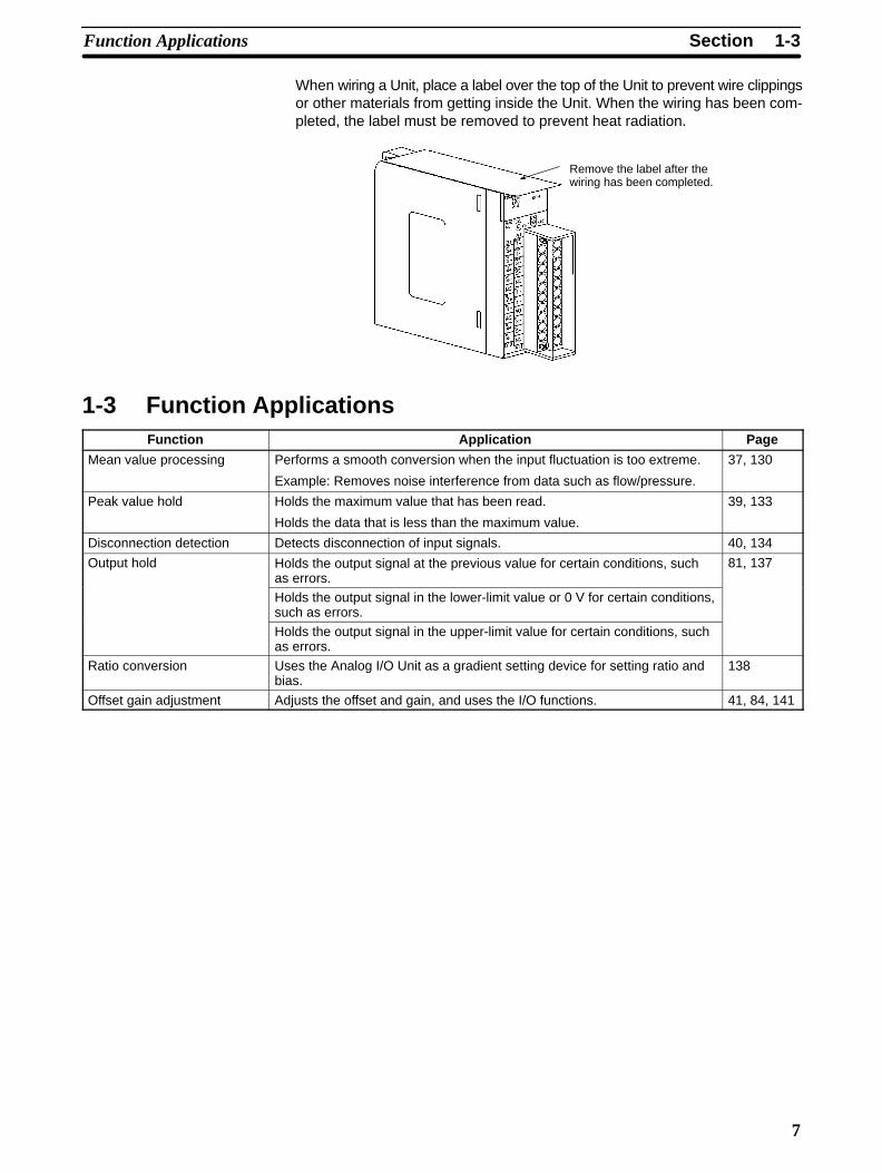
When wiring a Unit, place a label over the top of the Unit to prevent wire clippingsor other materials from getting inside the Unit. When the wiring has been com-pleted, the label must be removed to prevent heat radiation.
Remove the label after thewiring has been completed.
1-3 Function ApplicationsFunction Application Page
Mean value processing Performs a smooth conversion when the input fluctuation is too extreme.
Example: Removes noise interference from data such as flow/pressure.
37, 130
Peak value hold Holds the maximum value that has been read.
Holds the data that is less than the maximum value.
39, 133
Disconnection detection Detects disconnection of input signals. 40, 134
Output hold Holds the output signal at the previous value for certain conditions, suchas errors.
81, 137
Holds the output signal in the lower-limit value or 0 V for certain conditions,such as errors.
Holds the output signal in the upper-limit value for certain conditions, suchas errors.
Ratio conversion Uses the Analog I/O Unit as a gradient setting device for setting ratio andbias.
138
Offset gain adjustment Adjusts the offset and gain, and uses the I/O functions. 41, 84, 141

9
SECTION 2Analog Input Units
This section explains how to use the CS1W-AD041/081 Analog Input Units.
2-1 Specifications 10. . . . . . . . . . . . . . . . . . . . . . . . . . . . . . . . . . . . . . . . . . . . . . . . . . . . . . . . . . . . 2-1-1 Specifications 10. . . . . . . . . . . . . . . . . . . . . . . . . . . . . . . . . . . . . . . . . . . . . . . . . . . . . 2-1-2 Input Function Block Diagram 12. . . . . . . . . . . . . . . . . . . . . . . . . . . . . . . . . . . . . . . 2-1-3 Input Specifications 13. . . . . . . . . . . . . . . . . . . . . . . . . . . . . . . . . . . . . . . . . . . . . . . .
2-2 Operating Procedure 15. . . . . . . . . . . . . . . . . . . . . . . . . . . . . . . . . . . . . . . . . . . . . . . . . . . . . . . 2-2-1 Procedure Examples 15. . . . . . . . . . . . . . . . . . . . . . . . . . . . . . . . . . . . . . . . . . . . . . .
2-3 Components and Switch Settings 21. . . . . . . . . . . . . . . . . . . . . . . . . . . . . . . . . . . . . . . . . . . . . 2-3-1 Indicators 22. . . . . . . . . . . . . . . . . . . . . . . . . . . . . . . . . . . . . . . . . . . . . . . . . . . . . . . . 2-3-2 Unit Number Switch 22. . . . . . . . . . . . . . . . . . . . . . . . . . . . . . . . . . . . . . . . . . . . . . . 2-3-3 Operation Mode Switch 23. . . . . . . . . . . . . . . . . . . . . . . . . . . . . . . . . . . . . . . . . . . . . 2-3-4 Voltage/Current Switch 24. . . . . . . . . . . . . . . . . . . . . . . . . . . . . . . . . . . . . . . . . . . . .
2-4 Wiring 24. . . . . . . . . . . . . . . . . . . . . . . . . . . . . . . . . . . . . . . . . . . . . . . . . . . . . . . . . . . . . . . . . . 2-4-1 Terminal Arrangement 24. . . . . . . . . . . . . . . . . . . . . . . . . . . . . . . . . . . . . . . . . . . . . . 2-4-2 Internal Circuitry 25. . . . . . . . . . . . . . . . . . . . . . . . . . . . . . . . . . . . . . . . . . . . . . . . . . 2-4-3 Voltage Input Disconnection 26. . . . . . . . . . . . . . . . . . . . . . . . . . . . . . . . . . . . . . . . . 2-4-4 Input Wiring Example 27. . . . . . . . . . . . . . . . . . . . . . . . . . . . . . . . . . . . . . . . . . . . . . 2-4-5 Input Wiring Considerations 27. . . . . . . . . . . . . . . . . . . . . . . . . . . . . . . . . . . . . . . . .
2-5 Exchanging Data with the CPU Unit 28. . . . . . . . . . . . . . . . . . . . . . . . . . . . . . . . . . . . . . . . . . 2-5-1 Outline of Data Exchange 28. . . . . . . . . . . . . . . . . . . . . . . . . . . . . . . . . . . . . . . . . . . 2-5-2 Unit Number Settings 29. . . . . . . . . . . . . . . . . . . . . . . . . . . . . . . . . . . . . . . . . . . . . . 2-5-3 Special I/O Unit Restart Bits 29. . . . . . . . . . . . . . . . . . . . . . . . . . . . . . . . . . . . . . . . . 2-5-4 Fixed Data Allocations 30. . . . . . . . . . . . . . . . . . . . . . . . . . . . . . . . . . . . . . . . . . . . . 2-5-5 I/O Refresh Data Allocations 32. . . . . . . . . . . . . . . . . . . . . . . . . . . . . . . . . . . . . . . . .
2-6 Analog Input Functions and Operating Procedures 35. . . . . . . . . . . . . . . . . . . . . . . . . . . . . . . 2-6-1 Input Settings and Conversion Values 35. . . . . . . . . . . . . . . . . . . . . . . . . . . . . . . . . . 2-6-2 Mean Value Processing 37. . . . . . . . . . . . . . . . . . . . . . . . . . . . . . . . . . . . . . . . . . . . . 2-6-3 Peak Value Hold Function 39. . . . . . . . . . . . . . . . . . . . . . . . . . . . . . . . . . . . . . . . . . . 2-6-4 Input Disconnection Detection Function 40. . . . . . . . . . . . . . . . . . . . . . . . . . . . . . . .
2-7 Adjusting Offset and Gain 41. . . . . . . . . . . . . . . . . . . . . . . . . . . . . . . . . . . . . . . . . . . . . . . . . . 2-7-1 Adjustment Mode Operational Flow 41. . . . . . . . . . . . . . . . . . . . . . . . . . . . . . . . . . . 2-7-2 Input Offset and Gain Adjustment Procedures 43. . . . . . . . . . . . . . . . . . . . . . . . . . .
2-8 Handling Errors and Alarms 49. . . . . . . . . . . . . . . . . . . . . . . . . . . . . . . . . . . . . . . . . . . . . . . . 2-8-1 Indicators and Error Flowchart 49. . . . . . . . . . . . . . . . . . . . . . . . . . . . . . . . . . . . . . . 2-8-2 Alarms Occurring at the Analog Input Unit 50. . . . . . . . . . . . . . . . . . . . . . . . . . . . . 2-8-3 Errors in the CPU Unit 52. . . . . . . . . . . . . . . . . . . . . . . . . . . . . . . . . . . . . . . . . . . . . 2-8-4 Restarting Special I/O Units 53. . . . . . . . . . . . . . . . . . . . . . . . . . . . . . . . . . . . . . . . . 2-8-5 Troubleshooting 53. . . . . . . . . . . . . . . . . . . . . . . . . . . . . . . . . . . . . . . . . . . . . . . . . . .
2-1SectionSpecifications
10
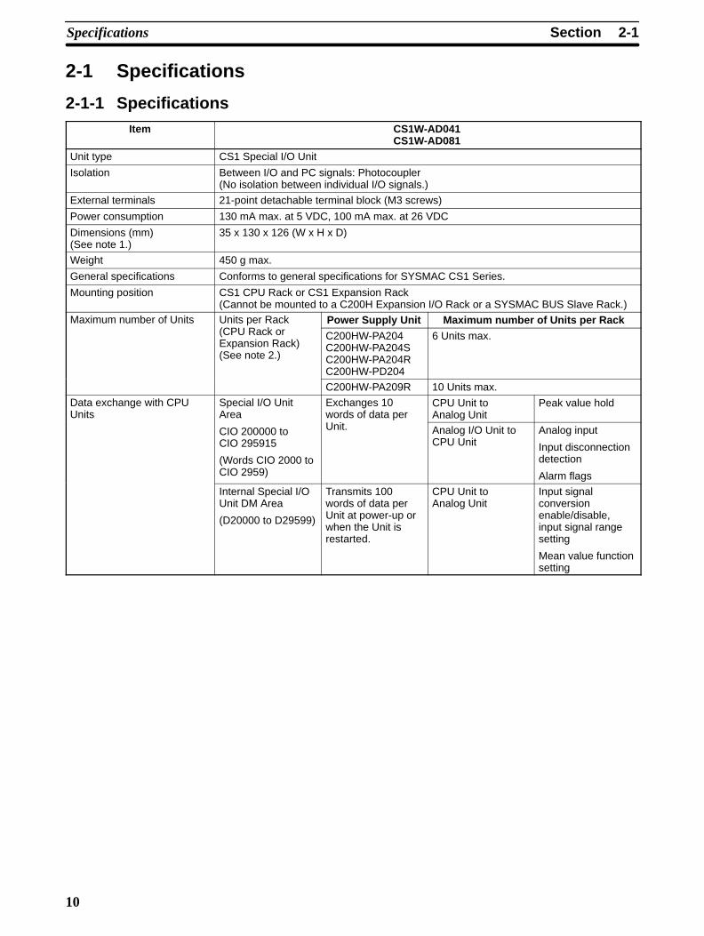
2-1 Specifications
2-1-1 SpecificationsItem CS1W-AD041
CS1W-AD081Unit type CS1 Special I/O Unit
Isolation Between I/O and PC signals: Photocoupler(No isolation between individual I/O signals.)
External terminals 21-point detachable terminal block (M3 screws)
Power consumption 130 mA max. at 5 VDC, 100 mA max. at 26 VDC
Dimensions (mm) (See note 1.)
35 x 130 x 126 (W x H x D)
Weight 450 g max.
General specifications Conforms to general specifications for SYSMAC CS1 Series.
Mounting position CS1 CPU Rack or CS1 Expansion Rack(Cannot be mounted to a C200H Expansion I/O Rack or a SYSMAC BUS Slave Rack.)
Maximum number of Units Units per Rack Power Supply Unit Maximum number of Units per Rack(CPU Rack orExpansion Rack)(See note 2.)
C200HW-PA204C200HW-PA204SC200HW-PA204RC200HW-PD204
6 Units max.
C200HW-PA209R 10 Units max.
Data exchange with CPUUnits
Special I/O UnitArea
Exchanges 10words of data per
CPU Unit toAnalog Unit
Peak value hold
CIO 200000 toCIO 295915
(Words CIO 2000 toCIO 2959)
Unit. Analog I/O Unit toCPU Unit
Analog input
Input disconnectiondetection
Alarm flags
Internal Special I/OUnit DM Area
(D20000 to D29599)
Transmits 100words of data perUnit at power-up orwhen the Unit isrestarted.
CPU Unit toAnalog Unit
Input signalconversionenable/disable,input signal rangesetting
Mean value functionsetting

2-1SectionSpecifications
11
Item CS1W-AD041CS1W-AD081
Input Specifications CS1W-AD041 CS1W-AD081
Number of analog inputs 4 8
Input signal range (See note 3.) 1 to 5 V0 to 5 V0 to 10 V–10 to 10 V4 to 20 mA(See note 4.)
Maximum rated input (for 1 point) (Seenote 5.)
Voltage Input: ±15 VCurrent Input: ±30 mA
Input impedance Voltage Input: 1 MΩ min.Current Input: 250 Ω (rated value)
Resolution 1/4,000 (full scale)
Converted output data 16-bit binary data
Accuracy(See note 6.)
23±2°C Voltage Input: ±0.2% of full scaleCurrent Input: ±0.4% of full scale
0°C to 55°C Voltage Input: ±0.4% of full scaleCurrent Input: ±0.6% of full scale
A/D conversion time (See note 7.) 1.0 ms/point max.
Functions Mean valueprocessing
Stores the last “n” data conversions in the buffer,and stores thethe mean value of the conversion values.
Buffer number: n = 2, 4, 8, 16, 32, 64
Peak value holding Stores the the maximum conversion value while the Peak ValueHold Bit is ON.
Input disconnectiondetection
Detects the disconnection and turns ON the DisconnectionDetection Flag.
Note 1. Refer to Dimensions on page 163 for details on the Unit’s dimensions.
2. The maximum number of Analog Input Units that can be mounted to oneRack varies depending on the current consumption of the other Unitsmounted to the Rack.
3. Input signal ranges can be set for each input.
4. Voltage input or current input are chosen by using the voltage/current switchat the back of the terminal block.
5. The Analog Input Unit must be operated according to the input specifica-tions provided here. Operating the Unit outside these specifications willcause the Unit to malfunction.
6. The accuracy is given for full scale. For example, an accuracy of ±0.2%means a maximum error of ±8 (BCD).
The default setting is adjusted for voltage input. To use current input, per-form the offset and gain adjustments as required.
7. A/D conversion time is the time it takes for an analog signal to be stored inmemory as converted data after it has been input. It takes at least one cyclebefore the converted data is read by the CPU Unit.

2-1SectionSpecifications
12
2-1-2 Input Function Block Diagram
Analog Input Unit CPU Unit
Special I/OUnit Area
Analoginput 1conver-sionvalue
I/Orefresh
Analog input 1
Analog input 2 Same as above.
Input dis-connectiondetection
Mean valueprocessingdisabled
Mean valueprocessingenabled
Peak valuehold functiondisabledA/D
Analog input 3
Analog input 4
Peak valuehold functionenabled
Same as above.
Same as above.
Analog input 5 Same as above. (See note.)
Analog input 6 Same as above. (See note.)
Analog input 7 Same as above. (See note.)
Analog input 8 Same as above. (See note.)
Note There are only four analog inputs for the CS1W-AD041.

2-1SectionSpecifications
13
2-1-3 Input SpecificationsIf signals that are outside the specified range provided below are input, the con-version values used will be either the maximum or minimum value.
Range: 1 to 5 V (4 to 20 mA)
1 V (4 mA)0.8 V (3.2 mA)
5 V (20 mA)5.2 V (20.8 mA)
Resolution: 4,000
Conversion value (16-bit binary data)
10680FA0
0000FF38
Analog input signal
Range: 0 to 10 V
0 V 10 V–0.5 V 10.5 V
10680FA0
0000FF38
Resolution: 4,000
Conversion value (16-bit binary data)
Analog input signal
2-1SectionSpecifications
14
Range: 0 to 5 V
0 V 5V–0.25 V 5.25 V
10680FA0
0000FF38
Resolution: 4,000
Conversion value (16-bit binary data)
Analog input signal
Range: –10 to 10 V
0 V 10 V11 V
089807D0
F830F768
0000
–10 V–11 V
Resolution: 4,000
Conversion value (16-bit binary data)
Analog input signal
Note The conversion values for a range of –10 to 10 V will be as follows:
16-bit binary data BCD
F768 –2200
: :
FFFF –1
0000 0
0001 1
: :
0898 2200

2-2SectionOperating Procedure
15
2-2 Operating ProcedureFollow the procedure outlined below when using Analog Input Units.
Installation and Settings1, 2, 3... 1. Set the DIP switch on the rear panel of the Unit to normal mode.
2. Set the voltage/current switch at the back of the terminal block.
3. Wire the Unit.
4. Use the unit number switch on the front panel of the Unit to set the unit num-ber.
5. Turn ON the power to the PC.
6. Create the Input tables.
7. Make the Special Input Unit DM Area settings.
• Set the input numbers to be used.
• Set the input signal ranges.
• Set the number of mean processing samplings.
8. Power up the PC again or turn the Special I/O Unit Restart Bit to ON and thenOFF again.
When the input for the connected devices needs to be calibrated, follow the pro-cedures in Offset Gain Adjustment below. Otherwise, skip to Operation below.
Offset and Gain Adjustment1, 2, 3... 1. Set the DIP switch on the rear panel of the Unit to adjustment mode.
2. Set the voltage/current switch at the back of the terminal block.
3. Turn ON the power to the PC.
4. Adjust the offset and gain.
5. Turn OFF the power to the PC.
6. Change the setting of the DIP switch on the rear panel of the Unit back tonormal mode.
Operation1, 2, 3... 1. Turn ON the power to the PC.
2. Ladder program
• Read conversion values or write set values by means of MOV(021) andXFER(070).
• Specify the peak hold function.
• Obtain disconnection notifications and error codes.
2-2-1 Procedure Examples
CS1W-AD081 CS1 CPU Unit
Unit No.: 1
Analog inputIN5: 0 to 10 V
IN6: 0 to 10 V
IN7: –10 to 10 V
IN8: Not used
IN1: 1 to 5 V
IN2: 1 to 5 V
IN3: 4 to 20 mA
IN4: 4 to 20 mA
Ladd
er P
rogr
am

2-2SectionOperating Procedure
16
Setting the Analog Input Unit
1, 2, 3... 1. Set the operation mode switch on the rear panel of the Unit. Refer to 2-3-3Operation Mode Switch for further details.
Turn OFF SW1 for normal mode
2. Set the voltage/current switch. Refer to 2-3-4 Voltage/Current Switch for fur-ther details.
Pins IN1 to IN8 correspond to analog inputs 1 to 8.
E.g., To use voltage input for analog inputs 1 and 2,turn OFF IN1 and IN2.
To use current input for analog inputs 3 and 4, turnON IN3 and IN4.
3. Mount and wire the Analog Input Unit. Refer to 1-2-1 Mounting Procedure,2-4 Wiring or 2-4-4 Input Wiring Example for further details.

2-2SectionOperating Procedure
17
4. Set the unit number switch. Refer to 2-3-2 Unit Number Switch for furtherdetails.
If the unit number is set to 1,words will be allocated to theSpecial I/O Unit Area CIO 2010to CIO 2019 and to the SpecialI/O Unit Area D20100 to D20199.
5. Turn ON the power to the PC.
Power ON
Creating I/O TablesAfter turning ON the power to the PC, be sure to create the I/O tables.
Peripheral port
2-2SectionOperating Procedure
18
Initial Data Settings
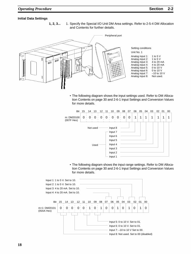
1, 2, 3... 1. Specify the Special I/O Unit DM Area settings. Refer to 2-5-4 DM Allocationand Contents for further details.
Peripheral port
Setting conditions
Unit No. 1
Analog input 1: 1 to 5 VAnalog input 2: 1 to 5 VAnalog input 3: 4 to 20 mAAnalog input 4: 4 to 20 mAAnalog input 5: 0 to 10 VAnalog input 6: 0 to 10 VAnalog input 7: –10 to 10 VAnalog input 8: Not used.
• The following diagram shows the input settings used. Refer to DM Alloca-tion Contents on page 30 and 2-6-1 Input Settings and Conversion Valuesfor more details.
15 14 13 12 11 10 09 08 07 06 05 01 0004 03 02
0 0 0 0 0 0 0 0 0 1 1 1 1 1 1 1
Bit
Input 4
Input 3
Input 2
Input 1
Used
m: DM20100(007F Hex)
Not used Input 8
Input 7
Input 6
Input 5
• The following diagram shows the input range settings. Refer to DM Alloca-tion Contents on page 30 and 2-6-1 Input Settings and Conversion Valuesfor more details.
15 14 13 12 11 10 09 08 07 06 05 01 0004 03 02
0 0 0 0 0 1 0 1 0 0 1 0 1 0 1 0
Bit
m+1: DM20101(05AA Hex)
Input 1: 1 to 5 V. Set to 10.
Input 2: 1 to 5 V. Set to 10.
Input 3: 4 to 20 mA. Set to 10.
Input 4: 4 to 20 mA. Set to 10.
Input 5: 0 to 10 V. Set to 01.
Input 6: 0 to 10 V. Set to 01.
Input 7: –10 to 10 V Set to 00.
Input 8: Not used. Set to 00 (disabled)

2-2SectionOperating Procedure
19
2. Restart the CPU Unit.
Power turned ON again (or Special I/O Unit Restart Bit is turned ON)
Creating Ladder Programs
Peripheral port
The data that is converted from analog to digital and output to CIO words (n + 1)to (n + 7) of the Special I/O Unit Area (CIO 2011 to CIO 2017), is stored in thespecified addresses D00100 to D00106 as signed binary values 0000 to 0FA0Hex.
• The following table shows the addresses used for analog input.
Input number Input signalrange
Input conversionvalue address
(n = CIO 2010)
(See note 1.)
Conversion dataholding address
(See note 2.)
1 1 to 5 V (n+1) = CIO 2011 D00100
2 1 to 5 V (n+2) = CIO 2012 D00101
3 4 to 20 mA (n+3) = CIO 2013 D00102
4 4 to 20 mA (n+4) = CIO 2014 D00103
5 0 to 10 V (n + 5)= CIO2015 D00104
6 0 to 10 V (n + 6)= CIO2016 D00105
7 –10 to 10 V (n + 7)= CIO2017 D00106
8 Not used --- ---
Note 1. The addresses are fixed according to the unit number of the Special I/O Unit.Refer to 2-3-2 Unit Number Switch for further details.

2-2SectionOperating Procedure
20
2. Set as required.
201900 Input 1 Disconnection Detection Flag (See note 3.)
201901 Input 2 Disconnection Detection Flag (See note 3.)
201902 Input 3 Disconnection Detection Flag (See note 3.)
201903 Input 4 Disconnection Detection Flag (See note 3.)
For 1 to 5 V, the hexadecimal value 0000to 0FA0 will be stored in CIO 2011, so ifthere is no disconnection (i.e., 201900 isOFF), CIO 2011 will be stored inD00100.
In the same way, for 1 to 5 V, CIO 2012will be stored in D00101.
In the same way, for 4 to 20 mA, CIO 2013will be stored in D00102.
In the same way, for 4 to 20 mA, CIO 2014will be stored in D00103.
MOV (021)
2011
D00100
MOV (021)
2012
D00101
MOV (021)
2013
D00102
MOV (021)
2014
D00103
3. The input Disconnection Detection Flag is allocated to bits 00 to 07 ofword (n + 9). Refer to Allocations for Normal Mode on page 33 for furtherdetails.
2-3SectionComponents and Switch Settings
21
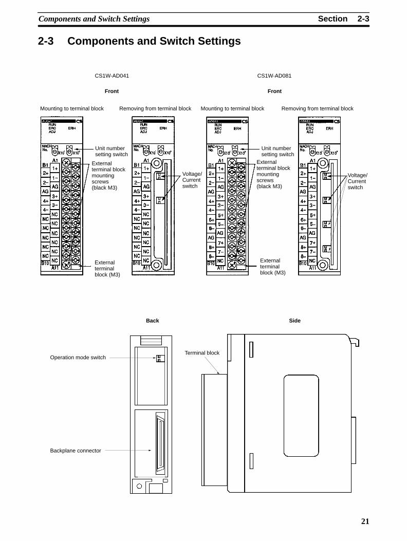
2-3 Components and Switch Settings
Unit numbersetting switch
External terminal blockmountingscrews (black M3)
Externalterminalblock (M3)
Front
Mounting to terminal block Removing from terminal block
Voltage/Currentswitch
CS1W-AD041 CS1W-AD081
Unit numbersetting switch
External terminal blockmountingscrews (black M3)
Externalterminalblock (M3)
Front
Mounting to terminal block Removing from terminal block
Voltage/Currentswitch
Operation mode switch
Backplane connector
Terminal block
SideBack

2-3SectionComponents and Switch Settings
22
The terminal block is attached by a connector. It can be removed by looseningthe two black mounting screws located at the top and bottom of the terminalblock.
Check to be sure that the black terminal block mounting screw is securely tight-ened to a torque of 0.5 N m.
Fasten the mounting screw.
Fasten the mounting screw.
2-3-1 Indicators
The indicators show the operating status of the Unit. The following table showsthe meanings of the indicators.
LED Meaning Indicator Operating statusRUN Operating Lit Operating in normal mode.(green) Not lit Unit has stopped exchanging data with
the CPU Unit.ERC (red) Error
detected byUnit
Lit Alarm has occurred (such asdisconnection detection) or initialsettings are incorrect.
Not lit Operating normally.
ADJ(yellow)
Adjusting Flashing Operating in offset/gain adjustmentmode.
Not lit Other than the above.
ERH (red) Error in theCPU Unit
Lit Error has occurred during dataexchange with the CPU Unit.
Not lit Operating normally.
2-3-2 Unit Number Switch
The CPU Unit and Analog Input Unit exchange data via the Special I/O Unit Areaand the Special I/O Unit DM Area. The Special I/O Unit Area and Special I/O UnitDM Area word addresses that each Analog Input Unit occupies are set by theunit number switch on the front panel of the Unit.

!
!
2-3SectionComponents and Switch Settings
23
Always turn OFF the power before setting the unit number. Use a flat-bladescrewdriver, being careful not to damage the slot in the screw. Be sure not toleave the switch midway between settings.
Switchsetting
Unitnumber
Special/O Unit Areaaddresses
Special I/O Unit DM Areaaddresses
0 Unit #0 CIO 2000 to CIO 2009 D20000 to D20099
1 Unit #1 CIO 2010 to CIO 2019 D20100 to D20199
2 Unit #2 CIO 2020 to CIO 2029 D20200 to D20299
3 Unit #3 CIO 2030 to CIO 2039 D20300 to D20399
4 Unit #4 CIO 2040 to CIO 2049 D20400 to D20499
5 Unit #5 CIO 2050 to CIO 2059 D20500 to D20599
6 Unit #6 CIO 2060 to CIO 2069 D20600 to D20699
7 Unit #7 CIO 2070 to CIO 2079 D20700 to D20799
8 Unit #8 CIO 2080 to CIO 2089 D20800 to D20899
9 Unit #9 CIO 2090 to CIO 2099 D20900 to D20999
10 Unit #10 CIO 2100 to CIO 2109 D21000 to D21099
~ ~ ~ ~
n Unit #n CIO 2000 + (n x 10) toCIO 2000 + (n x 10) + 9
D20000 + (n x 100) to D20000 + (n x 100) + 99
~ ~ ~ ~
95 Unit #95 CIO 2950 to CIO 2959 D29500 to D29599
Note If two or more Special I/O Units are assigned the same unit number, an “UNITNo. DPL ERR” error (in the Programming Console) will be generated (A40113will turn ON) and the PC will not operate.
2-3-3 Operation Mode Switch
The operation mode switch on the back panel of the Unit is used to set the opera-tion mode to either normal mode or adjustment mode (for adjusting offset andgain).
Pin number Mode
1 2
OFF OFF Normal mode
ON OFF Adjustment mode
Caution Do not set the pins to any combination other than those shown in the abovetable. Be sure to set pin 2 to OFF.
Caution Be sure to turn OFF the power to the PC before installing or removing the Unit.
!
2-4SectionWiring
24
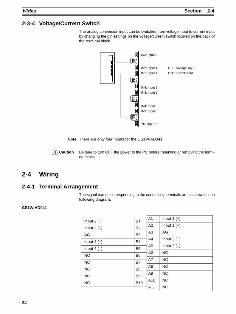
2-3-4 Voltage/Current SwitchThe analog conversion input can be switched from voltage input to current inputby changing the pin settings on the voltage/current switch located on the back ofthe terminal block.
IN2: Input 1
IN1: Input 4
OFF: Voltage input
ON: Current input
IN4: Input 3
IN3: Input 6
IN2: Input 2
IN4: Input 5
IN3: Input 8
IN2: Input 7
Note There are only four inputs for the CS1W-AD041.
Caution Be sure to turn OFF the power to the PC before mounting or removing the termi-nal block.
2-4 Wiring
2-4-1 Terminal ArrangementThe signal names corresponding to the connecting terminals are as shown in thefollowing diagram.
CS1W-AD041
Input 2 (+) B1
Input 2 (–) B2
AG B3
Input 4 (+) B4
Input 4 (–) B5
NC B6
NC B7
NC B8
NC B9
NC B10
A1
A2
A3
A4
A5
A6
A7
A8
A9
A10
A11
Input 1 (+)
Input 1 (–)
AG
Input 3 (+)
Input 3 (–)
NC
NC
NC
NC
NC
NC

2-4SectionWiring
25
CS1W-AD081
Input 2 (+) B1
Input 2 (–) B2
AG B3
Input 4 (+) B4
Input 4 (–) B5
Input 6 (+) B6
Input 6 (–) B7
AG B8
Input 8 (+) B9
Input 8 (–) B10
A1
A2
A3
A4
A5
A6
A7
A8
A9
A10
A11
Input 1 (+)
Input 1 (–)
AG
Input 3 (+)
Input 3 (–)
Input 5 (+)
Input 5 (–)
AG
Input 7 (+)
Input 7 (–)
NC
Note 1. The analog input numbers that can be used are set in the Data Memory(DM).
2. The input signal ranges for individual inputs are set in the Data Memory(DM). They can be set in units of input numbers.
3. The AG terminals (A8, B8) are connected to the 0-V analog circuit in theUnit. Connecting shielded input lines can improve noise resistance.
Do not make any connections to the NC terminals.
2-4-2 Internal CircuitryThe following diagrams show the internal circuitry of the analog input section.
Input Circuitry
1 MΩ
15 kΩ 15 kΩ
15 kΩ 15 kΩ
AG (common to all inputs)
Input (+)
Input (–)
AG(analog0 V)
Input circuitandconversioncircuit
1 MΩ
Voltage/currentinput switch
250 Ω

2-4SectionWiring
26
Internal Configuration
Bus interface
Indicators/Switch
MPU
RegulatorInsulation-typeDC-to-DC converter
Oscillator
Division
CS1 Series
EEPROM
Pho
toco
uple
r in
sula
tion
RAM ROM
Multi-plexerandamplifier
A/D converter
INPUT
Externallyconnectedterminal
2-4-3 Voltage Input Disconnection
Connected device #1
24 VDC
Connecteddevice #2
Note If the connected device #2 in the above example outputs 5 V and the power sup-ply is shared by 2 channels as shown in the above diagram, approximately onethird of the voltage, or 1.6 V, will be input at input 1.

2-4SectionWiring
27
When voltage inputs are used and a disconnection occurs, separate the powersupply at the side of the connected devices or use an insulating device (isolator)for each input to avoid the following problems.When the power supply at the connected devices is shared and section A or B isdisconnected, power will flow in the direction of the broken line and the outputvoltage of the other connected devices will be reduced to between a third to ahalf of the voltage. If 1 to 5 V is used and the reduced voltage output, disconnec-tion may not be detectable. If section C is disconnected, the power at the (–)input terminal will be shared and disconnection will not be detectable.For current inputs, sharing the power supply between the connected devices willnot cause any problems.
2-4-4 Input Wiring Example
Input 2
Input 6
CS1W-AD081
Shield
See note 4See note 4
Input 1
Input 4
Input 8
Input 3
Input 5
Input 7
Shield
Shield
Shield
Note 1. When using current inputs, pins IN1 to IN8 (pins IN1 to IN4 for theCS1W-AD041) of the voltage/current switch must be set to ON. Refer to2-3-4 Voltage/Current Switch for further details.
2. For inputs that are not used, either set to “0: Not used” in the input numbersettings (refer to 2-6-1 Input Settings and Conversion Values) or short-cir-cuit the voltage input terminals (V+) and (V–).
3. Crimp-type terminals must be used for terminal connections, and thescrews must be tightened securely. Use M3 screws and tighten them to atorque of 0.5 N m.
4. When connecting the shield of the analog input cables to the Unit’s AG ter-minals, as shown in the above diagram, use a wire that is 30 cm max. inlength if possible.
6.0 mm max.
6.0 mm max.M3 screw
Fork type
Round type
Connecting shielded cable to the Unit’s AG terminals can improve noise resis-tance.
2-4-5 Input Wiring ConsiderationsWhen wiring inputs, apply the following points to avoid noise interference andoptimize Analog Input Unit performance.• Use two-core shielded twisted-pair cables for input connections.

2-5SectionExchanging Data with the CPU Unit
28
• Route input cables separately from the AC cable, and do not run the Unit’scables near a main circuit cable, high voltage cable, or a non-PC load cable.
• If there is noise interference from power lines (if, for example, the power supplyis shared with electrical welding devices or electrical discharge machines, or ifthere is a high-frequency generation source nearby) install a noise filter at thepower supply input area.
2-5 Exchanging Data with the CPU Unit
2-5-1 Outline of Data ExchangeData is exchanged between the CPU Unit and the CS1W-AD041/081 AnalogInput Unit via the Special I/O Unit Area (for data used to operate the Unit) and theSpecial I/O Unit DM Area (for data used for initial settings).
I/O Refresh DataAnalog input conversion values, which are used as data for Unit operation, areallocated in the Special I/O Unit Area of the CPU Unit according to the unit num-ber, and are exchanged during I/O refreshing.
Fixed DataThe Unit’s fixed data, such as the analog input signal ranges and the number ofoperational mean value buffers is allocated in the Special I/O Unit DM Area ofthe CPU Unit according to the unit number, and is exchanged when the power isturned ON or the Unit is restarted.
CS1 CPU Unit CS1W-AD041/081 Analog Input Unit
Special I/O Unit Area I/O Refresh Data
Analog inputs
Analog inputs
DM (Data Memory) Area
Input signal range
Number of opera-tional mean valuebuffers
I/O refresh
Power ON orUnit restart
Exchanges analog input val-ues during data refresh.
See 2-5-5 I/ORefresh DataAllocations fordetails.
Transmits fixed data suchas analog input signalranges and number ofoperational mean valuebuffers.
See 2-5-4 FixedData Allocationsfor details.
2000 + n x 10
2000 + n x 10 + 9
D20000 + n x 100
D20000 + n x 100 + 99
10words
100words
Fixed Data
:
:

2-5SectionExchanging Data with the CPU Unit
29
2-5-2 Unit Number Settings
The Special I/O Unit Area and Special I/O Unit DM Area word addresses thateach Analog Input Unit occupies are set by the unit number switch on the frontpanel of the Unit.
Switchsetting
Unitnumber
Special/O Unit Areaaddresses
Special I/O Unit DM Areaaddresses
0 Unit #0 CIO 2000 to CIO 2009 D20000 to D20099
1 Unit #1 CIO 2010 to CIO 2019 D20100 to D20199
2 Unit #2 CIO 2020 to CIO 2029 D20200 to D20299
3 Unit #3 CIO 2030 to CIO 2039 D20300 to D20399
4 Unit #4 CIO 2040 to CIO 2049 D20400 to D20499
5 Unit #5 CIO 2050 to CIO 2059 D20500 to D20599
6 Unit #6 CIO 2060 to CIO 2069 D20600 to D20699
7 Unit #7 CIO 2070 to CIO 2079 D20700 to D20799
8 Unit #8 CIO 2080 to CIO 2089 D20800 to D20899
9 Unit #9 CIO 2090 to CIO 2099 D20900 to D20999
10 Unit #10 CIO 2100 to CIO 2109 D21000 to D21099
~ ~ ~ ~
n Unit #n CIO 2000 + (n x 10) toCIO 2000 + (n x 10) + 9
D20000 + (n x 100) to D20000 + (n x 100) + 99
~ ~ ~ ~
95 Unit #95 CIO 2950 to CIO 2959 D29500 to D29599
Note If two or more Special I/O Units are assigned the same unit number, an “UNITNo. DPL ERR” error (in the Programming Console) will be generated (A40113will turn ON) and the PC will not operate.
2-5-3 Special I/O Unit Restart Bits
To restart the Unit operations after changing the contents of the data memory orcorrecting an error, turn ON the power to the PC again or turn the Special I/O UnitRestart Bit ON and then OFF again.
Special I/OUnit Area word
address
Function
A50200 Unit No. 0 Restart Bit Restarts the Unit when turned
A50201 Unit No. 1 Restart Bit ON and then OFF again.
~ ~
A50215 Unit No. 15 Restart Bit
A50300 Unit No. 16 Restart Bit
~ ~
A50715 Unit No. 95 Restart Bit
Note If the error is not corrected by restarting the Unit or turning the Special I/O UnitRestart Bit ON and then OFF again, replace the Analog Input Unit.

2-5SectionExchanging Data with the CPU Unit
30
2-5-4 Fixed Data AllocationsDM Allocation and Contents The initial settings of the Analog Input Unit are set according to the data allo-
cated in the Special I/O Unit DM Area. Settings, such as the inputs used and theanalog input signal range must be set in this area.
D(m+1)
D(m)
D20300 to D20399
D20400 to D20499
D20500 to D20599
D20000 to D20099
D20100 to D20199
D20200 to D20299
D20900 to D20999
D20600 to D20699
D20700 to D20799
D20800 to D20899
SYSMAC CS1-series PC CS1W-AD041/081 Analog Input Unit
(Fixed Data Area)
Unit #0
Unit #1
Unit #2
Unit #3
Unit #4
Unit #5
Unit #6
Unit #7
Unit #8
Unit #9
(Special I/O Unit DM Area)
Word
D29500 to D29599
D21000 to D21099
~
D20000 + (n x 100) toD20000 + (n x 100) + 99
Unit #10
~
Unit #n
~
Unit #95
D(m+2 tom+5) (See note)
Input conversionpermission loopmode setting
Input signal rangeData is automaticallytransferred to each unitnumber when the poweris turned ON, or whenthe Special I/O UnitRestart Bit is turned ON.
m = 20000 + (100 x unit number)
~
Note D(m+9) for the CS1W-AD081.
Sets number ofsamplings for meanvalue processing
Note 1. The Special I/O Unit DM Area words that are occupied by the Analog InputUnit are set using the unit number switch on the front panel of the Unit. Referto 2-5-2 Unit Number Settings for details on the method used to set the unitnumber switch.
2. If two or more Special I/O Units are assigned the same unit number, an“UNIT No. DPL ERR” error (in the Programming Console) will be generated(A40113 will turn ON) and the PC will not operate.
The following table shows the allocation of DM words and bits for both normaland adjustment mode.
CS1W-AD041
DM word Bits
15 14 13 12 11 10 9 8 7 6 5 4 3 2 1 0D(m) Not used. Input use setting
Input4
Input3
Input2
Input1
D(m+1) Not used. Input signal range setting
Input 4 Input 3 Input 2 Input 1
D(m+2) Input 1: Mean value processing setting
D(m+3) Input 2: Mean value processing setting
D(m+4) Input 3: Mean value processing setting
D(m+5) Input 4:Mean value processing setting
DM Allocation Contents

2-5SectionExchanging Data with the CPU Unit
31
CS1W-AD081
DM word Bits
15 14 13 12 11 10 9 8 7 6 5 4 3 2 1 0D(m) Not used. Input use setting
Input8
Input7
Input6
Input5
Input4
Input3
Input2
Input1
D(m+1) Input signal range setting
Input 8 Input 7 Input 6 Input 5 Input 4 Input 3 Input 2 Input 1
D(m+2) Input 1: Mean value processing setting
D(m+3) Input 2: Mean value processing setting
D(m+4) Input 3: Mean value processing setting
D(m+5) Input 4: Mean value processing setting
D(m+6) Input 5: Mean value processing setting
D(m+7) Input 6: Mean value processing setting
D(m+8) Input 7: Mean value processing setting
D(m+9) Input 8: Mean value processing setting
Note For the DM word addresses, m = 20000 + (100 x unit number).
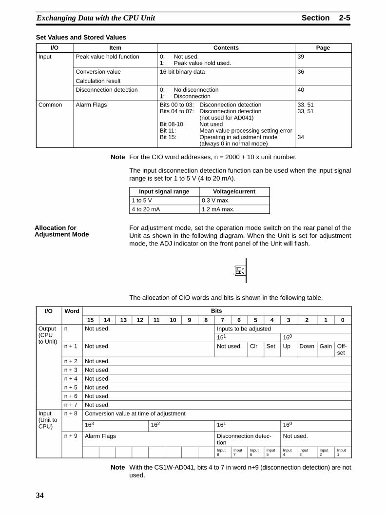
Set Values and Stored ValuesItem Contents Page
Input Use setting 0: Not used.1: Used.
35
Input signal range 00: –10 to 10 V01: 0 to 10 V10: 1 to 5 V/4 to 20 mA (See note 1.)11: 0 to 5 V
36
Mean value processingsetting
0000: Mean value processing for 2 buffers (See note 3.)0001: No mean value processing0002: Mean value processing for 4 buffers0003: Mean value processing for 8 buffers0004: Mean value processing for 16 buffers0005: Mean value processing for 32 buffers0006: Mean value processing for 64 buffers
37
Note 1. The input signal range of “1 to 5 V” and “4 to 20 mA” is switched using thepins of the voltage/current switch. Refer to 2-3-4 Voltage/Current Switch fordetails.
2. The default of mean value processing setting is set to “Mean value proces-sing for 2 buffers.” Refer to 2-6-2 Mean Value Processing.

2-5SectionExchanging Data with the CPU Unit
32
2-5-5 I/O Refresh Data AllocationsI/O refresh data for the Analog Input Unit is exchanged according to the alloca-tions in the Special I/O Unit Area.
CIO n + 1to CIO n + 9
CIO n
CIO 2030 to CIO 2039
CIO 2040 to CIO 2049
CIO 2050 to CIO 2059
CIO 2000 to CIO 2009
CIO 2010 to CIO 2019
CIO 2020 to CIO 2029
CIO 2090 to CIO 2099
CIO 2060 to CIO 2069
CIO 2070 to CIO 2079
CIO 2080 to CIO 2089
SYSMAC CS1-series PC CS1W-AD041/081 Analog Input Unit
IN refresh
(I/O Refresh Data Area)
Unit #0
Unit #1
Unit #2
Unit #3
Unit #4
Unit #5
Unit #6
Unit #7
Unit #8
Unit #9
(Special I/O Unit Area)
At the I/O refresh by thePC, outputs (CPU toUnit) and inputs (Unit toCPU) are refreshed inorder with every cycle.
OUT refresh
Allocated words
CIO 2950 to CIO 2959
CIO 2100 to CIO 2109
~
CIO 2000 + (n x 10) toCIO 2000 + (n x 10) + 9
Unit #10
~
Unit #n
~
Unit #95
Normal mode
CIO n + 8to CIO n + 9
CIO n toCIO n + 7
IN refresh
OUT refresh
Adjustment mode
n = 2000 + (10 x unit number)
~
I/O refresh
Note 1. The Special I/O Unit Area words that are occupied by the Analog Input Unitare set using the unit number switch on the front panel of the Unit. Refer to2-5-2 Unit Number Settings for details on the method used to set the unitnumber switch.
2. If two or more Special I/O Units are assigned the same unit number, an“UNIT No. DPL ERR” error (in the Programming Console) will be generated(A40113 will turn ON) and the PC will not operate.

2-5SectionExchanging Data with the CPU Unit
33
For normal mode, set the operation mode switch on the rear panel of the Unit asshown in the following diagram.
The allocation of words and bits in the CIO Area is shown in the following table.
CS1W-AD041
I/O Word Bits
15 14 13 12 11 10 9 8 7 6 5 4 3 2 1 0
Output n Not used. Peak value hold(CPU toUnit)
Input4
Input3
Input2
Input1
Input n + 1 Input 1 conversion value(Unit to 163 162 161 160CPU)
n + 2 Input 2 conversion value
n + 3 Input 3 conversion value
n + 4 Input 4 conversion value
n + 5 Not used
n + 6 Not used
n + 7 Not used
n + 8 Not used
n + 9 Alarm Flags Not used Disconnection detec-tionInput4
Input3
Input2
Input1
CS1W-AD081
I/O Word Bits
15 14 13 12 11 10 9 8 7 6 5 4 3 2 1 0
Output n Not used. Peak value hold(CPU toUnit)
Input8
Input7
Input6
Input5
Input4
Input3
Input2
Input1
Input n + 1 Input 1 conversion value(Unit to 163 162 161 160CPU)
n + 2 Input 2 conversion value
n + 3 Input 3 conversion value
n + 4 Input 4 conversion value
n + 5 Input 5 conversion value
n + 6 Input 6 conversion value
n + 7 Input 7 conversion value
n + 8 Input 8 conversion value
n + 9 Alarm Flags Disconnection detectionInput8
Input7
Input6
Input5
Input4
Input3
Input2
Input1
Allocations for NormalMode
2-5SectionExchanging Data with the CPU Unit
34
Set Values and Stored Values
I/O Item Contents Page
Input Peak value hold function 0: Not used.1: Peak value hold used.
39
Conversion value
Calculation result
16-bit binary data 36
Disconnection detection 0: No disconnection1: Disconnection
40
Common Alarm Flags Bits 00 to 03: Disconnection detectionBits 04 to 07: Disconnection detection
(not used for AD041)Bit 08-10: Not usedBit 11: Mean value processing setting errorBit 15: Operating in adjustment mode
(always 0 in normal mode)
33, 5133, 51
34
Note For the CIO word addresses, n = 2000 + 10 x unit number.
The input disconnection detection function can be used when the input signalrange is set for 1 to 5 V (4 to 20 mA).
Input signal range Voltage/current
1 to 5 V 0.3 V max.
4 to 20 mA 1.2 mA max.
For adjustment mode, set the operation mode switch on the rear panel of theUnit as shown in the following diagram. When the Unit is set for adjustmentmode, the ADJ indicator on the front panel of the Unit will flash.
The allocation of CIO words and bits is shown in the following table.
I/O Word Bits
15 14 13 12 11 10 9 8 7 6 5 4 3 2 1 0Output n Not used. Inputs to be adjusted(CPU 161 160to Unit)
n + 1 Not used. Not used. Clr Set Up Down Gain Off-set
n + 2 Not used.
n + 3 Not used.
n + 4 Not used.
n + 5 Not used.
n + 6 Not used.
n + 7 Not used.
Input n + 8 Conversion value at time of adjustment(Unit toCPU) 163 162 161 160
n + 9 Alarm Flags Disconnection detec-tion
Not used.
Input8
Input7
Input6
Input5
Input4
Input3
Input2
Input1
Note With the CS1W-AD041, bits 4 to 7 in word n+9 (disconnection detection) are notused.
Allocation forAdjustment Mode

2-6SectionAnalog Input Functions and Operating Procedures
35
Refer to 2-7-1 Adjustment Mode Operational Flow for further details.
Item Contents
Input to be adjusted Sets input to be adjusted.Leftmost digit: 2 (fixed)Rightmost digit: 1 to 8 (1 to 4 for CS1W-AD041)
Offset (Offset Bit) When ON, adjusts offset error.
Gain (Gain Bit) When ON, adjusts gain error.
Down (Down Bit) Decrements the adjustment value while ON.
Up (Up Bit) Increments the adjustment value while ON.
Set (Set Bit) Sets adjusted value and writes to EEPROM.
Clr (Clear Bit) Clears adjusted value. (Returns to default status)
Conversion value foradjustment
The conversion value for adjustment is stored as 16bits of binary data.
Disconnection detection 0: No disconnection1: Disconnection
Alarm Flags Bit 12: Input value is outside adjustment limits (inadjustment mode)Bit 13: Input number setting error (in adjustmentmode)Bit 14: EEPROM write error (in adjustment mode)Bit 15: Operating in adjustment mode
(always 1 in adjustment mode)
Note For the CIO word addresses, n = 2000 + (10 x unit number).
The input disconnection detection function can be used when the input signalrange is set for 1 to 5 V (4 to 20 mA).
Input signal range Voltage/current
1 to 5 V 0.3 V max.
4 to 20 mA 1.2 mA max.
2-6 Analog Input Functions and Operating Procedures
2-6-1 Input Settings and Conversion ValuesThe Analog Input Unit converts analog inputs specified by input numbers 1 to 8(1 to 4 for CS1W-AD041) only. To specify the analog inputs to be used, turn ONfrom a Programming Device the D(m) bits in the DM Area shown in the followingdiagram.
15 14 13 12 11 10 09 08 07 06 05 04 03 02 01 00Bit
D(m)
Inpu
t 2
Inpu
t 1
0: Not used
1: Used
Inpu
t 4
Inpu
t 3
Inpu
t 6
Inpu
t 5
Inpu
t 8
Inpu
t 7
Note There are only four inputs for the CS1W-AD041.
The analog input sampling interval can be shortened by setting any unused inputnumbers to 0.
Sampling interval = (1 ms) x (Number of inputs used)The word for inputs that have been set to “Not used” will always be “0000.”For the DM word addresses, m = 20000 + (100 x unit number)
Set Values and StoredValues
Input Numbers

2-6SectionAnalog Input Functions and Operating Procedures
36
Any of four types of input signal range (–10 to 10 V, 0 to 10 V, 1 to 5 V, and 4 to20 mA) can be selected for each of the inputs. To specify the input signal rangefor each input, set from a Programming Device the D(m + 1) bits in the DM Areaas shown in the following diagram.
15 14 13 12 11 10 09 08 07 06 05 04 03 02 01 00Bit
DM (m+1)
Inpu
t 2
Inpu
t 1
00: -10 to 10 V01: 0 to 10 V10: 1 to 5 V / 4 to 20 mA11: 0 to 5 V
Inpu
t 4
Inpu
t 3
Inpu
t 6
Inpu
t 5
Inpu
t 8
Inpu
t 7Note There are only four inputs for the CS1W-AD041.
Note 1. For the DM word addresses, m = 20000 + (100 x unit number)
2. The input signal range of “1 to 5 V” or “4 to 20 mA” is switched using the volt-age/current switch.
3. After making the DM settings from a Programming Device, it will be neces-sary to either power up the PC again or turn ON the Special I/O Unit RestartBit in order to transfer the contents of the DM settings to the Special I/O Unit.
Analog input conversion values are stored for each input number, in CIO wordsn+1 to n+8. With the CS1W-AD041, the values are stored in CIO words n+1 ton+4.
Word Function Stored value
n+1 Input 1 conversion value 16-bit binary data
n+2 Input 2 conversion value
n+3 Input 3 conversion value
n+4 Input 4 conversion value
n+5 Input 5 conversion value
n+6 Input 6 conversion value
n+7 Input 7 conversion value
n+8 Input 8 conversion value
Note For the CIO word addresses, n = 2000 + (10 x unit number).
Use MOV(021) or XFER(070) to read conversion values in the user program.
In this example, the conversion data from only one input is read. (The unit num-ber is 0.)
MOV(021)
2001
D00001
Input conditionConversion data in CIO word2001 (input number 1) is readto D 00001.
Input Signal Range
Reading ConversionValues
Example 1

2-6SectionAnalog Input Functions and Operating Procedures
37
In this example, the conversion data from multiple inputs is read. (The unit num-ber is 0.)
XFER(070)
#0004
2001
D00001
Input conditionConversion data in CIO words2001 to 2004 (input numbers1 to 4) is read to D00001 andD00004.
For details regarding conversion value scaling, refer to Scaling on page 168.
2-6-2 Mean Value ProcessingThe Analog Input Unit can compute the mean value of the conversion values ofanalog inputs that have been previously sampled. Mean value processinginvolves an operational mean value in the history buffers, so it has no effect onthe data refresh cycle. (The number of history buffers that can be set to usemean value processing is 2, 4, 8, 16, 32, or 64.)
Conversion data Buffer 1
Buffer 2
Buffer 3
Buffer 4
Buffer n
(Mean valueprocessing)
Conversion value
(Values stored inCIO words n+1 ton+8)
(Discarded)
When “n” number of history buffers are being used, the first conversion data willbe stored for all “n” number of history buffers immediately data conversion hasbegun or after a disconnection is restored.
When mean value processing is used together with the peak value hold function,the mean value will be held.
To specify whether or not mean value processing is to be used, and to specify thenumber of history buffers for mean data processing, use a Programming Deviceto make the settings in D(m+2) to D(m+9) as shown in the following table. (Withthe CS1W-AD041, make the settings in D(m+2) to D(m+5).)
DM word Function Set value
D(m+2) Input 1 mean value processing 0000: Mean value processing with 2 buffers
D(m+3) Input 2 mean value processing 0001: No mean value processing
D(m+4) Input 3 mean value processing0002: Mean value processing with 4 buffers0003: Mean value processing with 8 buffers
D(m+5) Input 4 mean value processing0003: Mean value processing with 8 buffers0004: Mean value processing with 16 buffers
D(m+6) Input 5 mean value processing 0005: Mean value processing with 32 buffers
D(m+7) Input 6 mean value processing0006: Mean value processing with 64 buffers
D(m+8) Input 7 mean value processing
D(m+9) Input 8 mean value processing
For the DM word addresses, m = 20000 + (100 x unit number)
Example 2
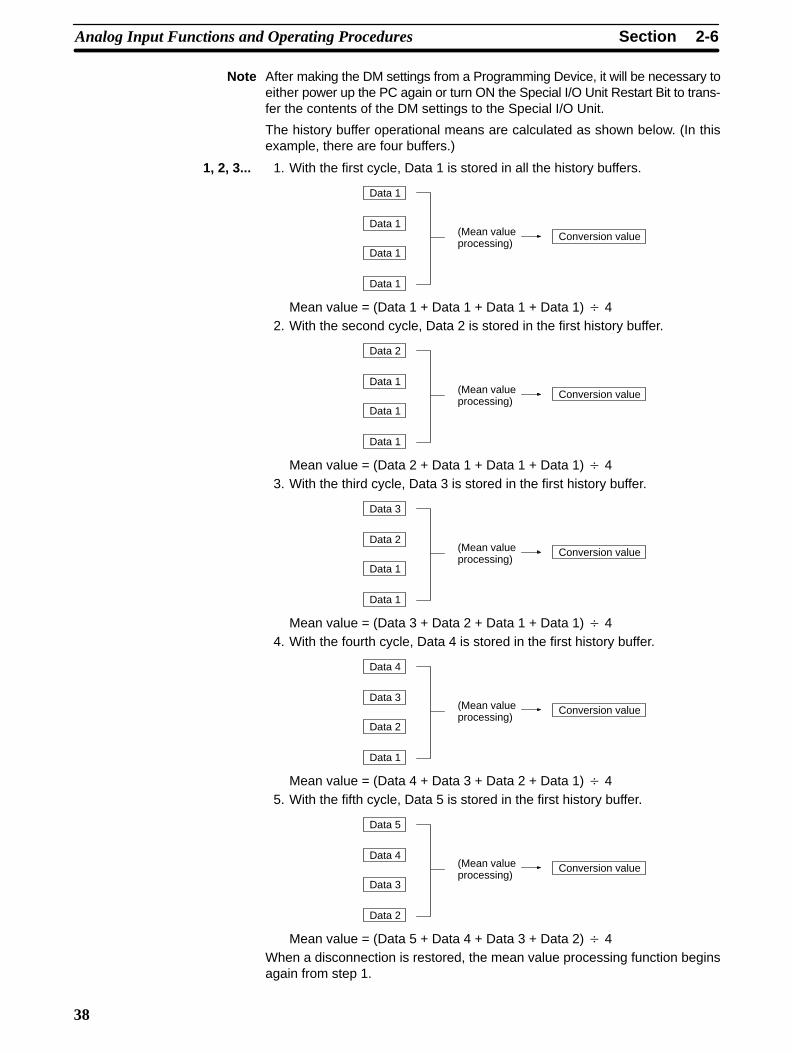
2-6SectionAnalog Input Functions and Operating Procedures
38
Note After making the DM settings from a Programming Device, it will be necessary toeither power up the PC again or turn ON the Special I/O Unit Restart Bit to trans-fer the contents of the DM settings to the Special I/O Unit.
The history buffer operational means are calculated as shown below. (In thisexample, there are four buffers.)
1, 2, 3... 1. With the first cycle, Data 1 is stored in all the history buffers.
(Mean valueprocessing)
Conversion value
Data 1
Data 1
Data 1
Data 1
Mean value = (Data 1 + Data 1 + Data 1 + Data 1) 42. With the second cycle, Data 2 is stored in the first history buffer.
(Mean valueprocessing)
Conversion value
Data 2
Data 1
Data 1
Data 1
Mean value = (Data 2 + Data 1 + Data 1 + Data 1) 43. With the third cycle, Data 3 is stored in the first history buffer.
(Mean valueprocessing)
Conversion value
Data 3
Data 2
Data 1
Data 1
Mean value = (Data 3 + Data 2 + Data 1 + Data 1) 44. With the fourth cycle, Data 4 is stored in the first history buffer.
(Mean valueprocessing)
Conversion value
Data 4
Data 3
Data 2
Data 1
Mean value = (Data 4 + Data 3 + Data 2 + Data 1) 45. With the fifth cycle, Data 5 is stored in the first history buffer.
(Mean valueprocessing)
Conversion value
Data 5
Data 4
Data 3
Data 2
Mean value = (Data 5 + Data 4 + Data 3 + Data 2) 4When a disconnection is restored, the mean value processing function beginsagain from step 1.

2-6SectionAnalog Input Functions and Operating Procedures
39
Note The default setting for mean value processing in the Analog Input Unit is meanvalue processing with 2 buffers. The response time for the default setting is dif-ferent from when there is no mean processing, as shown in the following dia-gram.
Input signal to the Unit (V)
Conversion data
Time (ms)
Time (ms)
t: Delay
V = 20 V (–10 to 10 V)(Actual measured value for 1 word)
Mean value processingwith 2 buffers
No mean valueprocessing
t = 6.5 ms t = 10.5 ms
The approximate value of t is as follows:
For 1 word:
t = n + (2 to 3) (ms)n = Number of buffers
For m words, 1 < m 8:
t = (n – 2) m + 10.5 (ms)
E.g., For 8 buffers and 4 words, t = 34.5 ms
Specify “no mean value processing” to follow conversion of a rapid change ininput signals.
2-6-3 Peak Value Hold FunctionThe peak value hold function holds the maximum digital conversion value forevery input (including mean value processing). This function can be used withanalog input. The following diagram shows how digital conversion values areaffected when the peak value hold function is used.
Peak value hold
Digital conversion value
t (Time)
Conversion value whenthe peak value holdfunction is used

2-6SectionAnalog Input Functions and Operating Procedures
40
The peak value hold function can be set individually for each input number byturning on the respective bits (00 to 07 for CS1W-AD081, 00 to 03 forCS1W-AD041) in CIO word n.
15 14 13 12 11 10 09 08 07 06 05 04 03 02 01 00Bit
Inpu
t 2
Inpu
t 1
Word n
The peak value hold function will be in effectfor the above input numbers while theirrespective bits are ON. The conversion valueswill be reset when the bits are turned OFF.
Inpu
t 4
Inpu
t 3
Inpu
t 6
Inpu
t 5
Inpu
t 8
Inpu
t 7
For the CIO word addresses, n = 2000 + (10 x unit number).In the following example, the peak value hold function is in effect for input num-ber 1, and the unit number is 0.
200000
Input conditionThe maximumconversiondata value isheld for inputnumber 1.
When mean value processing is used together with the peak value hold function,the mean value will be held.As long as the peak value hold function is in effect, the peak value hold will beheld even in the event of a disconnection.When the load to the CPU Unit is disconnected, the Peak Value Hold Bits (bits 00to 07 of the word n for CS1W-AD081, bits 00 to 03 of the word n forCS1W-AD041) are cleared and the peak value hold function is disabled.
2-6-4 Input Disconnection Detection FunctionWhen an input signal range of 1 to 5 V (4 to 20 mA) is used, input circuit discon-nections can be detected. The detection conditions for each of the input signalranges are shown in the following table. (see note)
Range Current/voltage
1 to 5 V 0.3 V max.
4 to 20 mA 1.2 mA max.
Note The current/voltage level will fluctuate according to the offset/gain adjustment.
The input disconnection detection signals for each input number are stored inbits 00 to 07 (00 to 03 for CS1W-AD041) of CIO word n+9. Specify these bits asexecution conditions to use disconnection detection in the user’s program.
15 14 13 12 11 10 09 08 07 06 05 04 03 02 01 00Bit
Inpu
t 6
Inpu
t 5
Word n+9
The respective bit turns ON when adisconnection is detected for a giveninput. When the disconnection isrestored, the bit turns OFF.
Inpu
t 8
Inpu
t 7
Inpu
t 2
Inpu
t 1
Inpu
t 4
Inpu
t 3
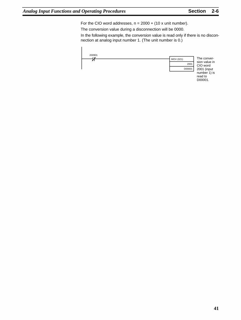
2-6SectionAnalog Input Functions and Operating Procedures
41
For the CIO word addresses, n = 2000 + (10 x unit number).
The conversion value during a disconnection will be 0000.
In the following example, the conversion value is read only if there is no discon-nection at analog input number 1. (The unit number is 0.)
MOV (021)
2001
D00001
200901The conver-sion value inCIO word2001 (inputnumber 1) isread toD00001.

2-7SectionAdjusting Offset and Gain
42
2-7 Adjusting Offset and Gain
2-7-1 Adjustment Mode Operational FlowThe adjustment mode enables the input of the connected devices to be cali-brated.
The offset voltage (or current) and gain voltage (or current) at the output deviceare entered as analog input conversion data 0000 and 0FA0 (07D0 if the range is±10 V) respectively.
For example, when using in the range 1 to 5 V, the actual output may be in therange 0.8 to 4.8 V, even though the specifications range for the external device is1 to 5 V. In this case, when an offset voltage of 0.8 V is output at the externaldevice, the conversion data at the Analog Input Unit will be FF38, and if a gainvoltage of 4.8 V is output, the conversion data will be 0EDA. The offset/gainadjustment function will, for this example, convert 0.8 V and 4.8 V to 0000 and0FA0 respectively and not to FF38 and 0EDA, as illustrated in the followingtable.
Offset/gain voltage atthe output device
Conversion data beforeadjustment
Conversion data afteradjustment
0.8 V FF38 0000
4.8 V 0EDA 0FA0

!
!
2-7SectionAdjusting Offset and Gain
43
The following diagram shows the flow of operations when using the adjustmentmode for adjusting offset and gain.
Change the operation mode switch on the rear panel of the Unit.
Turn ON the PC.
When adjusting another input number
When adjusting the same input number
Set the input number.
Offset adjustment
Offset Bit ON (Bit 0 of CIO wordn+1 turns ON.)
Samplinginput
(Add inputs so thatconversion valuebecomes 0.)
Set Bit ON (Bit 4 of CIO wordn+1 turns ON.)
Turn OFF power to the PC.
Change the operation mode switch on the rear panel of the Unit.
Set the operation mode switch to normal mode.
Set the operation mode switch to adjustment mode.
The ADJ indicator will flash while in adjustment mode.
Start up the PC in PROGRAM mode.
Write the input number to be adjustedin the rightmost byte of CIO word n.
Gain adjustment
Gain Bit ON (Bit 1 of CIO wordn+1 turns ON.)
Input adjustment
Set Bit ON (Bit 4 of CIO wordn+1 turns ON.)
(Add inputs so thatconversion value ismaximized.)
Samplinginput
Input adjustment
Caution Be sure to turn OFF the power to the PC before changing the setting of theoperation mode switch.
Caution Set the PC to PROGRAM mode when using the Analog Input Unit in adjustmentmode. If the PC is in MONITOR mode or RUN mode, the Analog Input Unit willstop operating, and the input values that existed immediately before this stop-page will be retained.

!
2-7SectionAdjusting Offset and Gain
44
Caution Always perform adjustments in conjunction with offset and gain adjustments.
Note Input adjustments can be performed more accurately in conjunction with meanvalue processing.
2-7-2 Input Offset and Gain Adjustment Procedures
To specify the input number to be adjusted, write the value to the rightmost byteof CIO word n as shown in the following diagram.
(Rightmost)(Leftmost)
Word n
Input to be adjusted (1 to 8)(1 to 4 for CS1W-AD041)
I/O specification2: Input (fixed)
For the CIO word addresses, n = 2000 + (10 x unit number).
The following example uses input number 1 adjustment for illustration. (The unitnumber is 0.)
CLR
SHIFTCH
*DM2
C0
A0
A0
AMON
CHG
2C
1B
WRITE
The CIO word (n+1) bits shown in the following diagram are used for adjustingoffset and gain.
15 14 13 12 11 10 09 08 07 06 05 04 03 02 01 00Bit
Word n+1
Cle
ar B
it
Set
Bit
Gai
n B
it
Offs
et B
it
Specifying Input Numberto be Adjusted
Bits Used for AdjustingOffset and Gain

2-7SectionAdjusting Offset and Gain
45
The procedure for adjusting the analog input offset is explained below. As shownin the following diagram, the offset is adjusted by sampling inputs so that theconversion value becomes 0.
10 V0
0FA0
Offset adjustment input range
Input signal range:0 to 10 V
The following example uses input number 1 adjustment for illustration. (The unitnumber is 0.)
1, 2, 3... 1. Turn ON bit 00 (the Offset Bit) of CIO word n+1. (Hold the ON status.)
CLR
SHIFTCONT
#2
C0
A0
A1
B0
A0
AMON
SET
The analog input’s digital conversion values while the Offset Bit is ON will bemonitored in CIO word n+8.
2. Check whether the input devices are connected.
A1
A1 +
–
+
–
Voltage input
Input 1
Current input
Input 1
For current input, check that the voltage/current switch is ON.
A2
A3
A2
A3
Offset Adjustment

!
!
2-7SectionAdjusting Offset and Gain
46
3. Input the voltage or current so that the conversion value becomes 0000. Thefollowing table shows the offset adjustment voltages and currents to beinput according to the input signal range.
Input signal range Input range Word (n+8) monitoringvalue
0 to 10 V –0.5 to 0.5 V FF38 to 00C8
–10 to 10 V –1.0 to 1.0 V
1 to 5 V 0.8 to 1.2 V
0 to 5 V –0.25 to 0.25 V
4 to 20 mA 3.2 to 4.8 mA
4. After inputting the voltage or current so that the conversion value for theanalog input terminal is 0000, turn ON bit 04 (the Set Bit) of CIO word n+1,and then turn it OFF again.
SHIFTCONT
#2
C0
A0
A1
B0
A4
EMON
SET
RESET
While the Offset Bit is ON, the offset value will be saved to the Unit’sEEPROM when the Set Bit turns ON.
5. To finish the offset adjustment, turn OFF bit 00 (the Offset Bit) of CIO wordn+1.
SHIFTCONT
#2
C0
A0
A1
B0
A0
AMON
RESET
Caution Do not turn OFF the power supply or restart the Unit while the Set Bit is ON (datais being written to the EEPROM). Otherwise, illegal data may be written in theUnit’s EEPROM and “EEPROM Errors” may occur when the power supply isturned ON or when the Unit is restarted, causing a malfunction.
Caution When making adjustments, be sure to perform both the offset adjustment andgain adjustment at the same time.
Note The EEPROM can be overwritten 50,000 times.

2-7SectionAdjusting Offset and Gain
47
The procedure for adjusting the analog input gain is explained below. As shownin the following diagram, the gain is adjusted by sampling inputs so that the con-version value is maximized.
10 V0
0FA0
Input signal range:0 to 10 V
Gain adjustment input range
The following example uses input number 1 adjustment for illustration. (The unitnumber is 0.)
1, 2, 3... 1. Turn ON bit 01 (the Gain Bit) of CIO word n+1. (Hold the ON status.)
SHIFTCONT
#2
C0
A0
A1
B0
A1
BMON
SET
The analog input’s digital conversion values while the Gain Bit is ON will bemonitored in CIO word n+8.
2. Check whether the input devices are connected.
+
–
+
–
Voltage input
Input 1
Current input
Input 1
For current input, check that the voltage/current switch is ON.
A1
A2
A3
A1
A2
A3
Gain Adjustment

!
!
2-7SectionAdjusting Offset and Gain
48
3. Input the voltage or current so that the conversion value is maximized (0FA0or 07D0). The following table shows the the gain adjustment voltages andcurrents to be input according to the input signal range.
Input signal range Input range Word (n+8) monitoringvalue
0 to 10 V 9.5 to 10.5 V 0ED8 to 1068
–10 to 10 V 9.0 to 11.0 V 0708 to 0898
1 to 5 V 4.8 to 5.2 V 0ED8 to 1068
0 to 5 V 4.75 to 5.25 V 0ED8 to 1068
4 to 20 mA 19.2 to 20.8 mA 0ED8 to 1068
4. With the voltage or current having been input so that the conversion valuefor the Analog Input Unit is maximized (0FA0 or 07D0), turn bit 04 (the SetBit) of CIO word n+1 ON and then OFF again.
SHIFTCONT
#2
C0
A0
A1
B0
A4
EMON
SET
RESET
While the Gain Bit is ON, the gain value will be saved to the Unit’s EEPROMwhen the Set Bit turns ON.
5. To finish the gain adjustment, turn OFF bit 01 (the Gain Bit) of CIO word n+1.
SHIFTCONT
#2
C0
A0
A1
B0
A1
BMON
RESET
Caution Do not turn OFF the power supply or restart the Unit while the Set Bit is ON (datais being written to the EEPROM). Otherwise, illegal data may be written in theUnit’s EEPROM and “EEPROM Errors” may occur when the power supply isturned ON or when the Unit is restarted, causing a malfunction.
Caution When making adjustments, be sure to perform both the offset adjustment andgain adjustment at the same time.
Note The EEPROM can be overwritten 50,000 times.

!
!
2-7SectionAdjusting Offset and Gain
49
Follow the procedure outlined below to return the offset and gain adjusted val-ues to their default settings.
The following example uses input number 1 adjustment for illustration. (The unitnumber is 0.)
1, 2, 3... 1. Turn ON bit 05 (the Clear Bit) of CIO word n+1. (Hold the ON status.)Regardless of the input value, 0000 will be monitored in CIO word n+8.
SHIFTCONT
#2
C0
A0
A1
B0
A5
FMON
SET
2. Turn bit 04 of CIO word n+1 ON and then OFF again.
SHIFTCONT
#2
C0
A0
A1
B0
A4
EMON
SET
RESET
While the Clear Bit is ON, the adjusted value will be cleared and reset to thedefault offset and gain values when the Set Bit turns ON.
3. To finish the clearing of adjusted values, turn OFF bit 05 (the Clear Bit) ofCIO word n+1.
SHIFTCONT
#2
C0
A0
A1
B0
A5
FMON
RESET
Caution Do not turn OFF the power supply or restart the Unit while the Set Bit is ON (datais being written to the EEPROM). Otherwise, illegal data may be written in theUnit’s EEPROM and “EEPROM Errors” may occur when the power supply isturned ON or when the Unit is restarted, causing a malfunction.
Caution When making adjustments, be sure to perform both the offset adjustment andgain adjustment at the same time.
Note The EEPROM can be overwritten 50,000 times.
Clearing Offset and GainAdjusted Values

2-8SectionHandling Errors and Alarms
50
2-8 Handling Errors and Alarms
2-8-1 Indicators and Error Flowchart
Indicators If an alarm or error occurs in the Analog Input Unit, the ERC or ERH indicators onthe front panel of the Unit will light.
Front panel of Unit
RUN
ERC
ADJ
ERH
LED Meaning Indicator Operating statusRUN Operating Lit Operating in normal mode.(green) Not lit Unit has stopped exchanging data with
the CPU Unit.ERC (red) Unit has
detected anerror
Lit Alarm has occurred (such asdisconnection detection) or initialsettings are incorrect.
Not lit Operating normally.
ADJ(yellow)
Adjusting Flashing Operating in offset/gain adjustmentmode.
Not lit Other than the above.
ERH (red) Error in theCPU Unit
Lit Error has occurred during dataexchange with the CPU Unit.
Not lit Operating normally.
Troubleshooting Procedure Use the following procedure for troubleshooting Analog Input Unit errors.
Error occurs.
Is the ERC indicatorlit?
Refer to 2-8-5Troubleshooting.
Yes
No
Is the RUN indicatorlit?
Yes
No
Alarm has occurred at the Analog Input Unit.(Refer to 2-8-2 Alarms Occurring at the Analog Input Unit.)
Check whether the initial settings for the Analog Input Unitare set correctly. (Refer to 2-8-2 Alarms Occurring at theAnalog Input Unit.)
Is the ERH indicatorlit?
Yes
No
Is the RUN indicatorlit?
Yes
No
Error detected by CPU Unit(Refer to 2-8-3 Errors in the CPU Unit.)
Check whether the unit number is set correctly. (Refer to 2-8-3 Errors in the CPU Unit.)
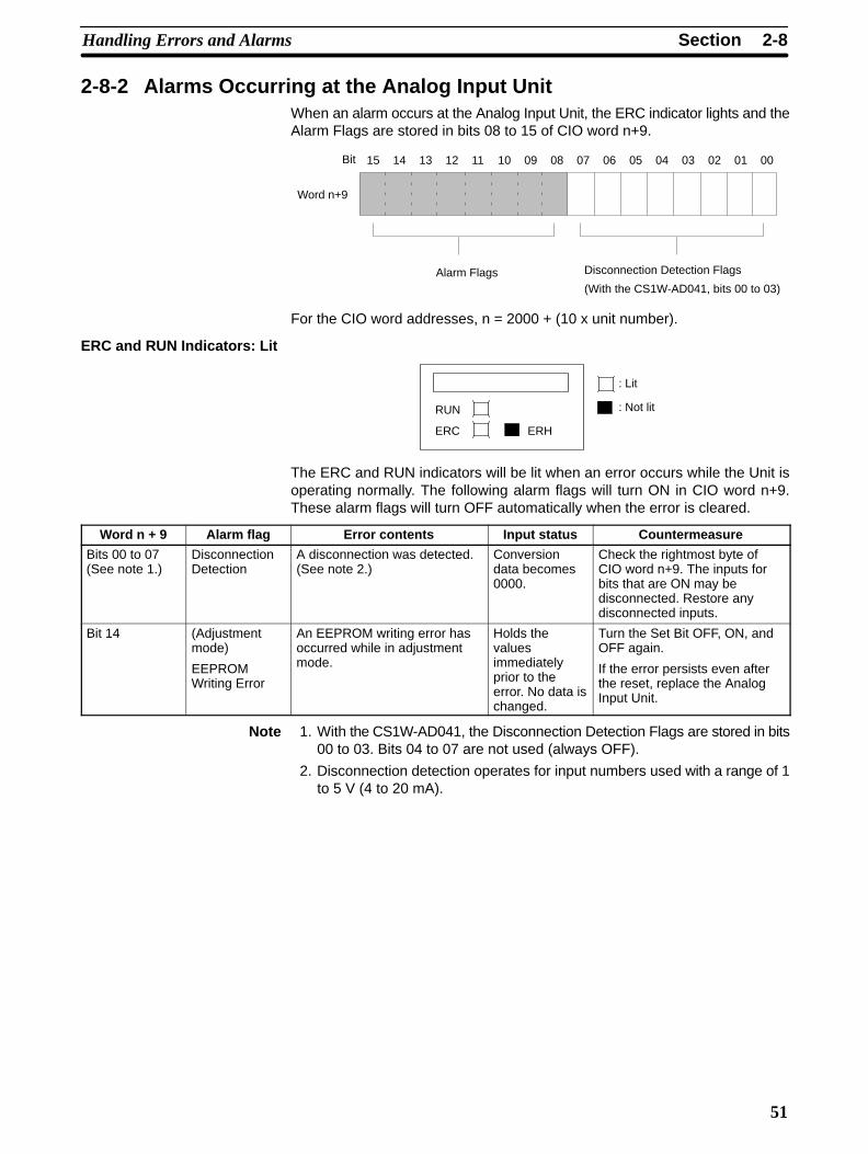
2-8SectionHandling Errors and Alarms
51
2-8-2 Alarms Occurring at the Analog Input UnitWhen an alarm occurs at the Analog Input Unit, the ERC indicator lights and theAlarm Flags are stored in bits 08 to 15 of CIO word n+9.
15 14 13 12 11 10 09 08 07 06 05 04 03 02 01 00Bit
Word n+9
Disconnection Detection Flags
(With the CS1W-AD041, bits 00 to 03)Alarm Flags
For the CIO word addresses, n = 2000 + (10 x unit number).
ERC and RUN Indicators: Lit
RUN
ERC ERH
: Lit
: Not lit
The ERC and RUN indicators will be lit when an error occurs while the Unit isoperating normally. The following alarm flags will turn ON in CIO word n+9.These alarm flags will turn OFF automatically when the error is cleared.
Word n + 9 Alarm flag Error contents Input status Countermeasure
Bits 00 to 07(See note 1.)
DisconnectionDetection
A disconnection was detected.(See note 2.)
Conversiondata becomes0000.
Check the rightmost byte ofCIO word n+9. The inputs forbits that are ON may bedisconnected. Restore anydisconnected inputs.
Bit 14 (Adjustmentmode)
EEPROMWriting Error
An EEPROM writing error hasoccurred while in adjustmentmode.
Holds thevaluesimmediatelyprior to theerror. No data ischanged.
Turn the Set Bit OFF, ON, andOFF again.
If the error persists even afterthe reset, replace the AnalogInput Unit.
Note 1. With the CS1W-AD041, the Disconnection Detection Flags are stored in bits00 to 03. Bits 04 to 07 are not used (always OFF).
2. Disconnection detection operates for input numbers used with a range of 1to 5 V (4 to 20 mA).

2-8SectionHandling Errors and Alarms
52
ERC Indicator and RUN Indicator: Lit, ADJ Indicator: Flashing
RUN
ERC ERH
ADJ
: Lit
: Flashing
: Not lit
This alarm will occur in the case of incorrect operation while in the adjustmentmode. In adjustment mode, the Adjustment Mode ON Flag will turn ON in bit 15of CIO word n+9.
Word n + 9 Alarm flag Error contents Input status Countermeasure
Bit 12 (Adjustmentmode)
Input ValueAdjustmentRangeExceeded
In adjustment mode, offset orgain cannot be adjustedbecause input value is out ofthe permissible range foradjustment.
Conversiondatacorrespondingto the inputsignal ismonitored inword n+8.
If making the adjustment bymeans of a connected inputdevice, first adjust the inputdevice before adjusting theAnalog Input Unit.
Bit 13 (Adjustmentmode)
Input NumberSetting Error
In adjustment mode,adjustment cannot beperformed because thespecified input number is notset for use or because thewrong input number isspecified.
Holds thevaluesimmediatelyprior to theerror. No data ischanged.
Check whether the word n inputnumber to be adjusted is setfrom 21 to 28 (21 to 24 forCS1W-AD041).
Check whether the inputnumber to be adjusted is set foruse by means of the DMsetting.
Bit 15 only ON (AdjustmentMode)
PC Error
The PC is in either MONITORor RUN mode while the AnalogInput Unit is operating inadjustment mode.
Holds thevaluesimmediatelyprior to theerror. No data ischanged.
Detach the Unit. Switch therear panel DIP switch pin toOFF. Restart the Unit in normalmode.
Note When a PC error occurs in the adjustment mode, the Unit will stop operating.(The input values immediately prior to the error are held.)
ERC Indicator: Lit, RUN Indicator: Not Lit
RUN
ERC ERH
: Lit
: Not lit
The ERC indicator will be lit when the initial settings for the Analog Input Unit arenot set correctly. The alarm flags for the following errors will turn ON in CIO wordn+9. These alarm flags will turn OFF when the error is cleared and the Unit isrestarted, or the Special I/O Unit Restart Bit is turned ON and then OFF again.
Word n + 9 Alarm flag Error contents Input status Countermeasure
Bit 11 Mean ValueProcessingSetting Error
The wrong number ofsamplings has been specifiedfor mean processing.
Conversiondoes not startand databecomes 0000.
Specify a number from 0000 to0006.

2-8SectionHandling Errors and Alarms
53
2-8-3 Errors in the CPU Unit
When errors occur in the CPU Unit or I/O bus, and I/O refresh with the Special I/OUnit is not performed correctly resulting in the Analog Input Unit malfunctioning,the ERH indicator will be lit.
ERH and RUN Indicators: Lit
RUN
ERC ERH
: Lit
: Not lit
The ERH and RUN indicators will be lit if an error occurs in the I/O bus causing aWDT (watchdog timer) error in the CPU Unit, resulting in incorrect I/O refreshwith the Analog Input Unit.
Turn ON the power supply again or restart the system.For further details, refer to CS1-series CS1G/H-CPU-E ProgrammableControllers Operation Manual (W339).
Error Error contents Input status
I/O bus error Error has occurred during dataexchange with the CPU Unit.
Conversion data becomes 0000.
CPU Unit monitoring error (seenote)
No response from CPU Unitduring fixed period.
Maintains the condition existingbefore the error.
CPU Unit WDT error Error has been generated inCPU Unit.
Changes to undefined state.
Note No error will be detected by the CPU Unit or displayed on the Programming Con-sole, because the CPU Unit is continuing operation.
ERH Indicator: Lit, RUN Indicator: Not Lit
RUN
ERC ERH
: Lit
: Not lit
The unit number for the Analog Input Unit has not been set correctly.
Error Error contents Input status
Duplicate Unit Number The same unit number has beenassigned to more than one Unitor the unit number was set to avalue other than 00 to 95.
Conversion does not start anddata becomes 0000.
Special I/O Unit Setting Error The Special I/O Units registeredin the I/O table are different fromthe ones actually mounted.

2-8SectionHandling Errors and Alarms
54
2-8-4 Restarting Special I/O Units
There are two ways to restart Special I/O Unit operation after having changedDM contents or having cleared the cause of an error. The first way is to power upthe PC again, and the second way is to turn the Special I/O Unit Restart Bit ONand then OFF again.
Special I/O Unit Restart Bits
Bits Functions
A50200 Unit #0 Restart Bit Turning the Restart Bit for any
A50201 Unit #1 Restart Bit Unit ON and then OFF again
~ ~restarts that Unit.
A50215 Unit #15 Restart Bit
A50300 Unit #16 Restart Bit
~ ~
A50715 Unit #95 Restart Bit
The conversion data becomes 0000 during restart.
If the error is not cleared even after turning the Special I/O Unit Restart Bit ONand then OFF again, then replace the Unit.
2-8-5 Troubleshooting
The following tables explain the probable causes of troubles that may occur, andthe countermeasures for dealing with them.
Probable cause Countermeasure Page
The input is not set for being used. Set the input to be used. 35
The peak value hold function is inoperation.
Turn OFF the peak value holdfunction if it is not required.
39
The input device is not working, theinput wiring is wrong, or there is adisconnection.
Using a tester, check to see if theinput voltage or current ischanging.
---
Use Unit’s alarm flags to check fora disconnection.
51
Probable cause Countermeasure Page
The input device’s signal rangedoes not match the input signalrange for the relevant input numberat the Analog Input Unit.
Check the specifications of theinput device, and match thesettings for the input signal ranges.
10
The offset and gain are notadjusted.
Adjust the offset and gain. 42
When using the 4 mA to 20 mArange, the voltage/current switch isnot turned ON.
Turn ON the voltage/currentswitch.
24
Probable cause Countermeasure Page
The input signals are beingaffected by external noise.
Change the shielded cableconnection to the Unit’s COMterminal.
27
Insert a 0.01-µF to 0.1-µF ceramiccapacitor or film capacitor betweenthe input’s (+) and (–) terminals.
---
Try increasing the number of meanvalue processing buffers.
37
Conversion Data DoesNot Change
Value Does Not Changeas Intended
Conversion Values areInconsistent

55
SECTION 3Analog Output Units
This section explains how to use the CS1W-DA041/08V/08C Analog Output Units.
3-1 Specifications 56. . . . . . . . . . . . . . . . . . . . . . . . . . . . . . . . . . . . . . . . . . . . . . . . . . . . . . . . . . . . 3-1-1 Specifications 56. . . . . . . . . . . . . . . . . . . . . . . . . . . . . . . . . . . . . . . . . . . . . . . . . . . . . 3-1-2 Output Function Block Diagram 58. . . . . . . . . . . . . . . . . . . . . . . . . . . . . . . . . . . . . . 3-1-3 Output Specifications 58. . . . . . . . . . . . . . . . . . . . . . . . . . . . . . . . . . . . . . . . . . . . . . .
3-2 Operating Procedure 60. . . . . . . . . . . . . . . . . . . . . . . . . . . . . . . . . . . . . . . . . . . . . . . . . . . . . . . 3-2-1 Procedure Examples 61. . . . . . . . . . . . . . . . . . . . . . . . . . . . . . . . . . . . . . . . . . . . . . .
3-3 Components and Switch Settings 66. . . . . . . . . . . . . . . . . . . . . . . . . . . . . . . . . . . . . . . . . . . . . 3-3-1 Indicators 67. . . . . . . . . . . . . . . . . . . . . . . . . . . . . . . . . . . . . . . . . . . . . . . . . . . . . . . . 3-3-2 Unit Number Switch 67. . . . . . . . . . . . . . . . . . . . . . . . . . . . . . . . . . . . . . . . . . . . . . . 3-3-3 Operation Mode Switch 68. . . . . . . . . . . . . . . . . . . . . . . . . . . . . . . . . . . . . . . . . . . . .
3-4 Wiring 69. . . . . . . . . . . . . . . . . . . . . . . . . . . . . . . . . . . . . . . . . . . . . . . . . . . . . . . . . . . . . . . . . . 3-4-1 Terminal Arrangement 69. . . . . . . . . . . . . . . . . . . . . . . . . . . . . . . . . . . . . . . . . . . . . . 3-4-2 Internal Circuitry 70. . . . . . . . . . . . . . . . . . . . . . . . . . . . . . . . . . . . . . . . . . . . . . . . . . 3-4-3 Output Wiring Example 71. . . . . . . . . . . . . . . . . . . . . . . . . . . . . . . . . . . . . . . . . . . . . 3-4-4 Output Wiring Considerations 71. . . . . . . . . . . . . . . . . . . . . . . . . . . . . . . . . . . . . . . .
3-5 Exchanging Data with the CPU Unit 72. . . . . . . . . . . . . . . . . . . . . . . . . . . . . . . . . . . . . . . . . . 3-5-1 Outline of Data Exchange 72. . . . . . . . . . . . . . . . . . . . . . . . . . . . . . . . . . . . . . . . . . . 3-5-2 Unit Number Settings 73. . . . . . . . . . . . . . . . . . . . . . . . . . . . . . . . . . . . . . . . . . . . . . 3-5-3 Special I/O Unit Restart Bits 73. . . . . . . . . . . . . . . . . . . . . . . . . . . . . . . . . . . . . . . . . 3-5-4 Fixed Data Allocations 74. . . . . . . . . . . . . . . . . . . . . . . . . . . . . . . . . . . . . . . . . . . . . 3-5-5 I/O Refresh Data Allocations 76. . . . . . . . . . . . . . . . . . . . . . . . . . . . . . . . . . . . . . . . .
3-6 Analog Output Functions and Operating Procedures 79. . . . . . . . . . . . . . . . . . . . . . . . . . . . . . 3-6-1 Output Settings and Conversions 79. . . . . . . . . . . . . . . . . . . . . . . . . . . . . . . . . . . . . . 3-6-2 Starting and Stopping Conversion 81. . . . . . . . . . . . . . . . . . . . . . . . . . . . . . . . . . . . . 3-6-3 Output Hold Function 81. . . . . . . . . . . . . . . . . . . . . . . . . . . . . . . . . . . . . . . . . . . . . . 3-6-4 Output Setting Errors 83. . . . . . . . . . . . . . . . . . . . . . . . . . . . . . . . . . . . . . . . . . . . . . .
3-7 Adjusting Offset and Gain 84. . . . . . . . . . . . . . . . . . . . . . . . . . . . . . . . . . . . . . . . . . . . . . . . . . 3-7-1 Adjustment Mode Operational Flow 84. . . . . . . . . . . . . . . . . . . . . . . . . . . . . . . . . . . 3-7-2 Output Offset and Gain Adjustment Procedures 86. . . . . . . . . . . . . . . . . . . . . . . . . .
3-8 Handling Errors and Alarms 94. . . . . . . . . . . . . . . . . . . . . . . . . . . . . . . . . . . . . . . . . . . . . . . . 3-8-1 Indicators and Error Flowchart 94. . . . . . . . . . . . . . . . . . . . . . . . . . . . . . . . . . . . . . . 3-8-2 Alarms Occurring at the Analog Output Unit 95. . . . . . . . . . . . . . . . . . . . . . . . . . . . 3-8-3 Errors in the CPU Unit 96. . . . . . . . . . . . . . . . . . . . . . . . . . . . . . . . . . . . . . . . . . . . . 3-8-4 Restarting Special I/O Units 97. . . . . . . . . . . . . . . . . . . . . . . . . . . . . . . . . . . . . . . . . 3-8-5 Troubleshooting 98. . . . . . . . . . . . . . . . . . . . . . . . . . . . . . . . . . . . . . . . . . . . . . . . . . .
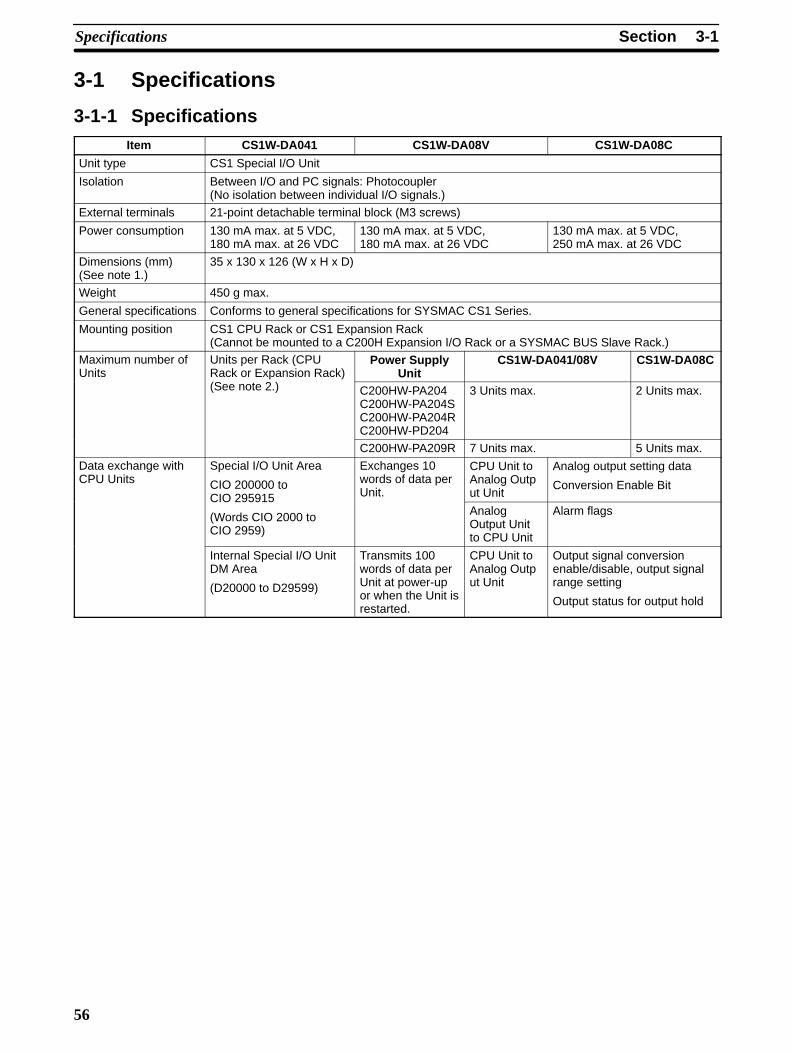
3-1SectionSpecifications
56
3-1 Specifications
3-1-1 SpecificationsItem CS1W-DA041 CS1W-DA08V CS1W-DA08C
Unit type CS1 Special I/O Unit
Isolation Between I/O and PC signals: Photocoupler(No isolation between individual I/O signals.)
External terminals 21-point detachable terminal block (M3 screws)
Power consumption 130 mA max. at 5 VDC,180 mA max. at 26 VDC
130 mA max. at 5 VDC, 180 mA max. at 26 VDC
130 mA max. at 5 VDC,250 mA max. at 26 VDC
Dimensions (mm) (See note 1.)
35 x 130 x 126 (W x H x D)
Weight 450 g max.
General specifications Conforms to general specifications for SYSMAC CS1 Series.
Mounting position CS1 CPU Rack or CS1 Expansion Rack(Cannot be mounted to a C200H Expansion I/O Rack or a SYSMAC BUS Slave Rack.)
Maximum number ofUnits
Units per Rack (CPURack or Expansion Rack)
Power SupplyUnit
CS1W-DA041/08V CS1W-DA08C
(See note 2.) C200HW-PA204C200HW-PA204SC200HW-PA204RC200HW-PD204
3 Units max. 2 Units max.
C200HW-PA209R 7 Units max. 5 Units max.
Data exchange withCPU Units
Special I/O Unit Area
CIO 200000 to
Exchanges 10words of data perUnit.
CPU Unit toAnalog Output Unit
Analog output setting data
Conversion Enable BitCIO 295915
(Words CIO 2000 toCIO 2959)
AnalogOutput Unitto CPU Unit
Alarm flags
Internal Special I/O UnitDM Area
(D20000 to D29599)
Transmits 100words of data perUnit at power-upor when the Unit isrestarted.
CPU Unit toAnalog Output Unit
Output signal conversionenable/disable, output signalrange setting
Output status for output hold

3-1SectionSpecifications
57
Item CS1W-DA08CCS1W-DA08VCS1W-DA041Output Specifications CS1W-DA041 CS1W-DA08V CS1W-DA08C
Number of analog outputs 4 8 8
Output signal range
(See note 3.)
1 to 5 V/4 to20 mA0 to 5 V0 to 10 V–10 to 10V
1 to 5 V0 to 5 V0 to 10 V–10 to 10 V
4 to 20 mA
Output impedance 0.5 Ω max.
Max. output current (for 1 point) 12 mA
Maximum permissible load resistance --- --- 600 ΩResolution 1/4,000 (full scale)
Set data 16-bit binary data
Accuracy 23±2°C Voltage output: ±0.3% of full scaleCurrent output: ±0.5% of full scale(See note 4.)
0°C to 55°C Voltage output: ±0.5% of full scaleCurrent output: ±0.8% of full scale
D/A conversion time (See note 5.) 1.0 ms/point max.
Functions Output hold function Outputs the specified output status (CLR, HOLD, or MAX) underany of the following circumstances.
When the Conversion Enable Bit is OFF. (See note 6.)
In adjustment mode, when a value other than the output number isoutput during adjustment.
When there is an output setting error or a fatal error occurs at thePC.
When the CPU Unit is on standby.
When the Load is OFF.
Note 1. Refer to Dimensions on page 163 for details on the Unit’s dimensions.
2. The maximum number of Analog Output Units that can be mounted to oneRack varies depending on the current consumption of the other Unitsmounted to the Rack.
3. Output signal ranges can be set for each output.
4. The accuracy is given for full scale. For example, an accuracy of ±0.3%means a maximum error of ±12 (BCD).
5. D/A conversion time is the time required for converting and outputting thePC data. It takes at least one cycle for the data stored in the PC to be read bythe Analog Output Unit.
6. When the operation mode for the CPU Unit is changed from RUN mode orMONITOR mode to PROGRAM mode, or when the power is turned ON, theOutput Conversion Enable Bit will turn OFF. The output status specifiedaccording to the output hold function will be output.

3-1SectionSpecifications
58
3-1-2 Output Function Block Diagram
Analog Output Unit CPU Unit
Special I/OUnit Area
Analogoutput 1set value
Output holdenabled
Output holddisabled
D/AAnalog output 1
Same as above.Analog output 2
Same as above.Analog output 3
Same as above.Analog output 4
Same as above.Analog output 5
Same as above.Analog output 7
Same as above.Analog output 8
Same as above.Analog output 6
Note There are only four analog outputs for the CS1W-DA041.
3-1-3 Output SpecificationsIf the set value is outside the specified range provided below, an output settingerror will occur, and the output specified by the output hold function will be out-put.
Range: 1 to 5 V (4 to 20 mA)
5.2 V (20.8 mA)5 V (20 mA)
1 V (4 mA)0.8 V (3.2 mA)
0000
FF38
0FA0
1068Resolution: 4,000
Set value (16-bit binary data)
Analog output signal

3-1SectionSpecifications
59
Range: 0 to 10 V
0000FF38
0FA0
1068
10.5 V10 V
0 V–0.5 V
Resolution: 4,000
Set value (16-bit binary data)
Analog output signal
Range: 0 to 5 V
0000FF38
0FA0
1068
5.25 V5 V
0 V–0.25 V
Resolution: 4,000
Set value (16-bit binary data)
Analog output signal
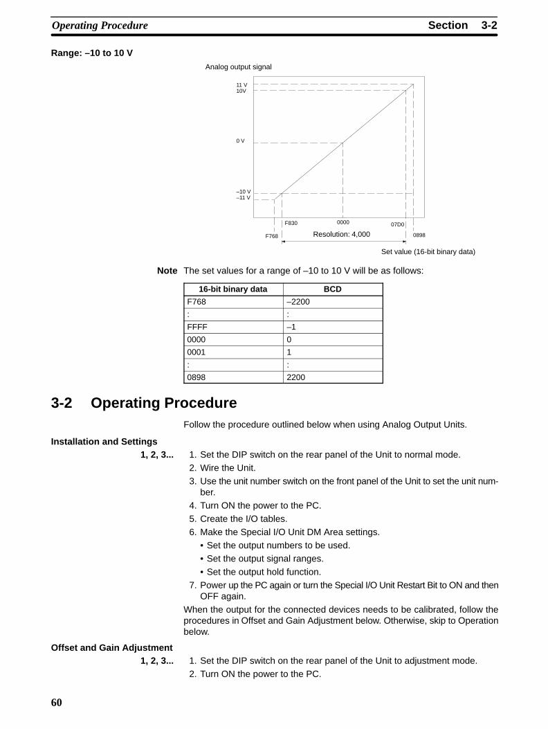
3-2SectionOperating Procedure
60
Range: –10 to 10 V
0000F830
F768
07D0
0898
0 V
–10 V–11 V
11 V10V
Resolution: 4,000
Set value (16-bit binary data)
Analog output signal
Note The set values for a range of –10 to 10 V will be as follows:
16-bit binary data BCD
F768 –2200
: :
FFFF –1
0000 0
0001 1
: :
0898 2200
3-2 Operating ProcedureFollow the procedure outlined below when using Analog Output Units.
Installation and Settings1, 2, 3... 1. Set the DIP switch on the rear panel of the Unit to normal mode.
2. Wire the Unit.
3. Use the unit number switch on the front panel of the Unit to set the unit num-ber.
4. Turn ON the power to the PC.
5. Create the I/O tables.6. Make the Special I/O Unit DM Area settings.
• Set the output numbers to be used.• Set the output signal ranges.
• Set the output hold function.7. Power up the PC again or turn the Special I/O Unit Restart Bit to ON and then
OFF again.
When the output for the connected devices needs to be calibrated, follow theprocedures in Offset and Gain Adjustment below. Otherwise, skip to Operationbelow.
Offset and Gain Adjustment1, 2, 3... 1. Set the DIP switch on the rear panel of the Unit to adjustment mode.
2. Turn ON the power to the PC.
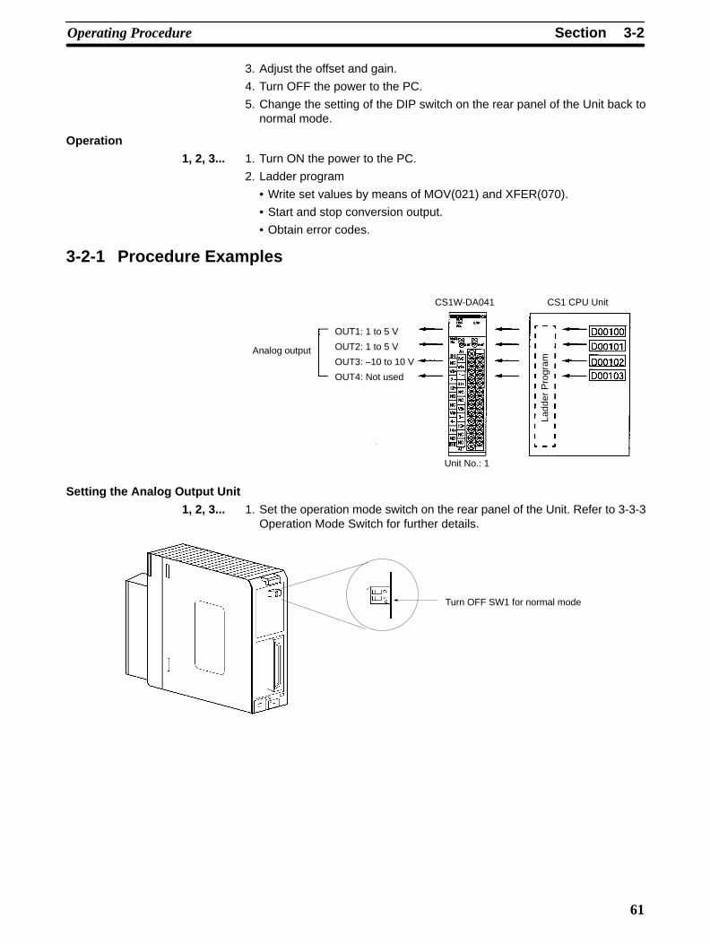
3-2SectionOperating Procedure
61
3. Adjust the offset and gain.
4. Turn OFF the power to the PC.
5. Change the setting of the DIP switch on the rear panel of the Unit back tonormal mode.
Operation
1, 2, 3... 1. Turn ON the power to the PC.
2. Ladder program
• Write set values by means of MOV(021) and XFER(070).
• Start and stop conversion output.
• Obtain error codes.
3-2-1 Procedure Examples
CS1W-DA041 CS1 CPU Unit
Unit No.: 1
Analog output
OUT1: 1 to 5 V
OUT2: 1 to 5 V
OUT3: –10 to 10 V
OUT4: Not used
Ladd
er P
rogr
am
Setting the Analog Output Unit
1, 2, 3... 1. Set the operation mode switch on the rear panel of the Unit. Refer to 3-3-3Operation Mode Switch for further details.
Turn OFF SW1 for normal mode

3-2SectionOperating Procedure
62
2. Mount and wire the Analog Output Unit. Refer to 1-2-1 Mounting Procedure,3-4 Wiring or 3-4-3 Output Wiring Example for further details.
3. Set the unit number switch. Refer to 3-3-2 Unit Number Switch for furtherdetails.
If the unit number is set to 1,words will be allocated to theSpecial I/O Unit Area CIO 2010to CIO 2019 and to the SpecialI/O Unit Area D20100 to D20199.
4. Turn ON the power to the PC.
Power ON
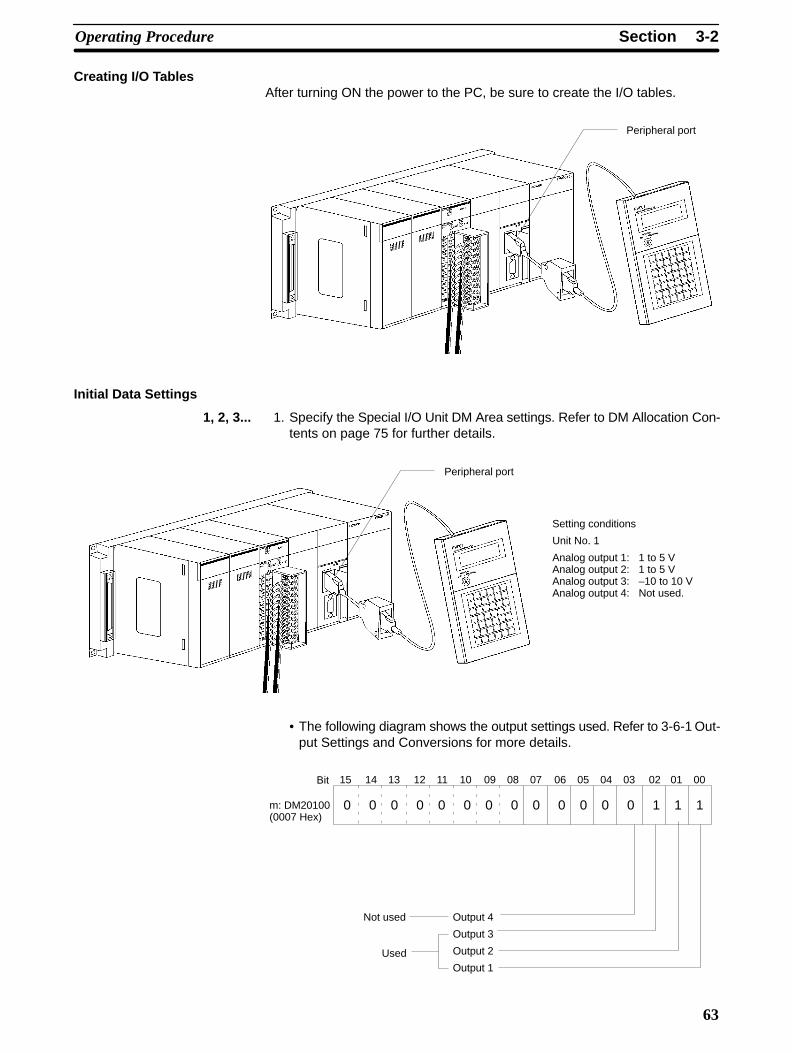
3-2SectionOperating Procedure
63
Creating I/O TablesAfter turning ON the power to the PC, be sure to create the I/O tables.
Peripheral port
Initial Data Settings
1, 2, 3... 1. Specify the Special I/O Unit DM Area settings. Refer to DM Allocation Con-tents on page 75 for further details.
Peripheral port
Setting conditions
Unit No. 1
Analog output 1: 1 to 5 VAnalog output 2: 1 to 5 VAnalog output 3: –10 to 10 VAnalog output 4: Not used.
• The following diagram shows the output settings used. Refer to 3-6-1 Out-put Settings and Conversions for more details.
15 14 13 12 11 10 09 08 07 06 05 01 0004 03 02
0 0 0 0 0 0 0 0 0 0 0 0 0 1 1 1
Bit
Not used Output 4
Output 3
Output 2
Output 1Used
m: DM20100(0007 Hex)

3-2SectionOperating Procedure
64
• The following diagram shows the output range settings. Refer to 3-6-1Output Settings and Conversions for more details.
15 14 13 12 11 10 09 08 07 06 05 01 0004 03 02
0 0 0 0 0 0 0 0 0 0 0 0 1 0 1 0
Bit
m+1: DM20101(000A Hex)
Output 1: 1 to 5 V. Set to 10.
Output 2: 1 to 5 V. Set to 10.
Output 3: –10 to 10 V. Set to 00.
Output 4: Not used. Set to 00 (disabled).
2. Restart the CPU Unit.
Power turned ON again (or Special I/O Unit Restart Bit is turned ON)
Creating Ladder ProgramsPeripheral port
The setting address D00200 is stored in words (n + 1) to (n + 3) of the Special I/OUnit Area (CIO 2011 to CIO 2013) as a signed binary value between 0000 to0FA0 Hex.The following table shows the addresses used for analog output.
Output number Output signalrange
Output settingaddress
(n = CIO 2010)
See note 1.
Originalconversion
address
1 1 to 5 V (n+1) = CIO 2011 D00200
2 0 to 10 V (n+2) = CIO 2012 D00201
3 –10 to 10 V (n+3) = CIO 2013 D00202
4 Not used. --- ---

3-2SectionOperating Procedure
65
Note 1. The addresses are set according to the unit number of the Special I/O Unit.Refer to 3-3-2 Unit Number Switch for further details.
2. Set as required.
D00200 is set in word CIO 2011.
D00201 is set in word CIO 2012.
D00202 is set in word CIO 2013.
To start analog output, turn ON theConversion Enable Bits 201000 to201002 (bits 00 to 03 of wordCIO 2010). See 3-6-2 Starting andStopping Conversion for details. Thedata in words CIO 2011 and CIO2012 will be output as 1 to 5 V, andthe data in CIO 2013 will be output as–10 to 10 V.
MOV (021)
D00200
2011
MOV (021)
D00201
2012
Execution condition
MOV (021)
D00202
2013
SET
201000
SET
201002
SET
201001
Execution condition

3-3SectionComponents and Switch Settings
66
3-3 Components and Switch Settings
Unit numbersetting switch
External terminalblock (M3)
External ter-minal blockmountingscrews(black M3)
Front
CS1W-DA041 CS1W-DA08V CS1W-DA08C
Operation mode switch
Backplane connector
Terminal block
SideBack

3-3SectionComponents and Switch Settings
67
The terminal block is attached by a connector. It can be removed by looseningthe two black mounting screws located at the top and bottom of the terminalblock.
Check to be sure that the black terminal block mounting screw is securely tight-ened to a torque of 0.5 N m.
Fasten the mounting screw.
Fasten the mounting screw.
3-3-1 Indicators
The indicators show the operating status of the Unit. The following table showsthe meanings of the indicators.
LED Meaning Indicator Operating statusRUN Operating Lit Operating in normal mode.(green) Not lit Unit has stopped exchanging data with
the CPU Unit.ERC (red) Error
detected byUnit
Lit Alarm has occurred (such asdisconnection detection) or initialsettings are incorrect.
Not lit Operating normally.
ADJ(yellow)
Adjusting Flashing Operating in offset/gain adjustmentmode.
Not lit Other than the above.
ERH (red) Error in theCPU Unit
Lit Error has occurred during dataexchange with the CPU Unit.
Not lit Operating normally.
3-3-2 Unit Number Switch
The CPU Unit and Analog Output Unit exchange data via the Special I/O UnitArea and the Special I/O Unit DM Area. The Special I/O Unit Area and SpecialI/O Unit DM Area word addresses that each Analog Output Unit occupies are setby the unit number switch on the front panel of the Unit.
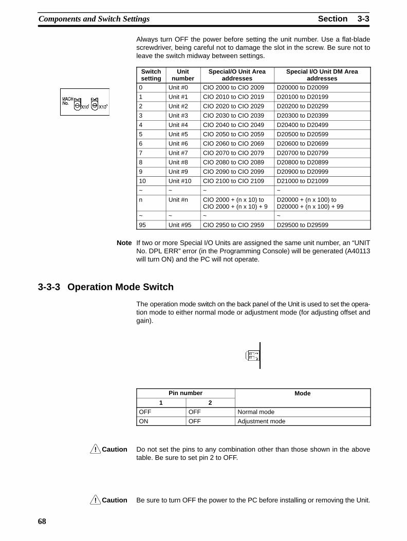
!
!
3-3SectionComponents and Switch Settings
68
Always turn OFF the power before setting the unit number. Use a flat-bladescrewdriver, being careful not to damage the slot in the screw. Be sure not toleave the switch midway between settings.
Switchsetting
Unitnumber
Special/O Unit Areaaddresses
Special I/O Unit DM Areaaddresses
0 Unit #0 CIO 2000 to CIO 2009 D20000 to D20099
1 Unit #1 CIO 2010 to CIO 2019 D20100 to D20199
2 Unit #2 CIO 2020 to CIO 2029 D20200 to D20299
3 Unit #3 CIO 2030 to CIO 2039 D20300 to D20399
4 Unit #4 CIO 2040 to CIO 2049 D20400 to D20499
5 Unit #5 CIO 2050 to CIO 2059 D20500 to D20599
6 Unit #6 CIO 2060 to CIO 2069 D20600 to D20699
7 Unit #7 CIO 2070 to CIO 2079 D20700 to D20799
8 Unit #8 CIO 2080 to CIO 2089 D20800 to D20899
9 Unit #9 CIO 2090 to CIO 2099 D20900 to D20999
10 Unit #10 CIO 2100 to CIO 2109 D21000 to D21099
~ ~ ~ ~
n Unit #n CIO 2000 + (n x 10) toCIO 2000 + (n x 10) + 9
D20000 + (n x 100) to D20000 + (n x 100) + 99
~ ~ ~ ~
95 Unit #95 CIO 2950 to CIO 2959 D29500 to D29599
Note If two or more Special I/O Units are assigned the same unit number, an “UNITNo. DPL ERR” error (in the Programming Console) will be generated (A40113will turn ON) and the PC will not operate.
3-3-3 Operation Mode Switch
The operation mode switch on the back panel of the Unit is used to set the opera-tion mode to either normal mode or adjustment mode (for adjusting offset andgain).
Pin number Mode
1 2
OFF OFF Normal mode
ON OFF Adjustment mode
Caution Do not set the pins to any combination other than those shown in the abovetable. Be sure to set pin 2 to OFF.
Caution Be sure to turn OFF the power to the PC before installing or removing the Unit.

3-4SectionWiring
69
3-4 Wiring
3-4-1 Terminal Arrangement
The signal names corresponding to the connecting terminals are as shown in thefollowing diagram.
CS1W-DA08V/08C
NC B1
Output 2 (+) B2
Output 4 (+)
B3
Output 4 (–)
B4
B5
Output 6 (+) B6
Output 6 (–) B7
Output 8 (+) B8
Output 8 (–) B9
NC B10
A1
A2
A3
A4
A5
A6
A7
A8
A9
A10
A11
Output 1 (+)
Output 1 (–)
Output 3 (+)
Output 3 (–)
Output 5 (+)
Output 5 (–)
Output 7(+)
Output 7 (–)
NC
NC
Output 2 (–)
NC
CS1W-DA041
NC B1
Output voltage 2 (+) B2
Output current 2 (+)
B3
NC
B4
B5
NC B6
Output voltage 4 (–) B7
Output 4 (–) B8
Output current 4 (+) B9
NC B10
A1
A2
A3
A4
A5
A6
A7
A8
A9
A10
A11
Output voltage 1 (+)
Output 1 (–)
Output current 1 (+)
NC
NC
Output voltage 3 (+)
Output 3 (–)
Output current 3 (+)
NC
NC
Output 2 (–)
NC
Note 1. The analog output numbers that can be used are set in the Data Memory(DM).
2. The output signal ranges for individual outputs are set in the Data Memory(DM). They can be set in units of output numbers.
3. The NC terminals are not connected to internal circuitry.
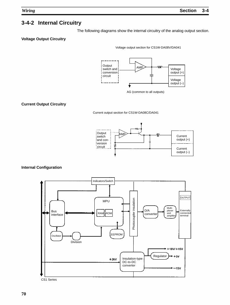
3-4SectionWiring
70
3-4-2 Internal CircuitryThe following diagrams show the internal circuitry of the analog output section.
Voltage Output Circuitry
Outputswitch andconversioncircuit
AMP Voltageoutput (+)
Voltageoutput (–)
AG (common to all outputs)
Voltage output section for CS1W-DA08V/DA041
Current Output Circuitry
Current output section for CS1W-DA08C/DA041
Outputswitchand con-versioncircuit
AMPCurrentoutput (+)
Currentoutput (–)
Internal Configuration
Bus interface
Indicators/Switch
MPUOUTPUT
RegulatorInsulation-typeDC-to-DC converter
Externallyconnectedterminal
Oscillator
Division
CS1 Series
EEPROM
Pho
toco
uple
r in
sula
tion
RAM ROMD/A converter
Multi-plexerandamplifier
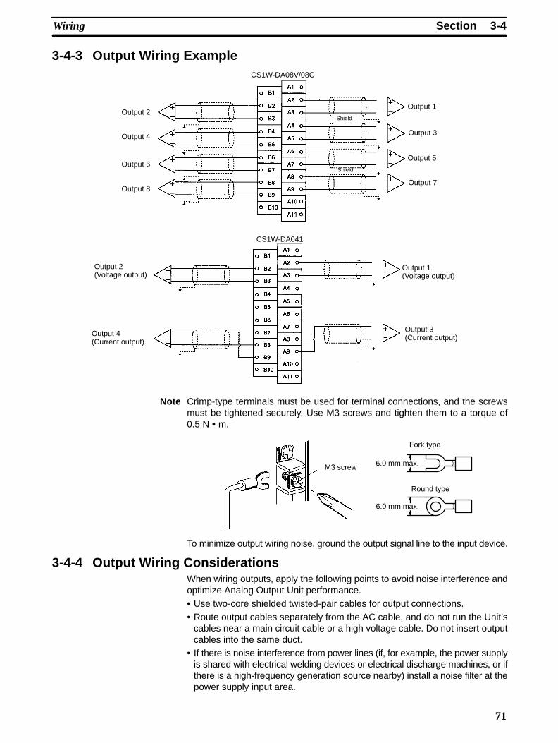
3-4SectionWiring
71
3-4-3 Output Wiring Example
Output 2
CS1W-DA08V/08C
Shield
Output 4
Output 6
Output 8
Shield
Output 1
Output 3
Output 5
Output 7
Output 2(Voltage output)
Output 4(Current output)
CS1W-DA041
Output 3(Current output)
Output 1(Voltage output)
Note Crimp-type terminals must be used for terminal connections, and the screwsmust be tightened securely. Use M3 screws and tighten them to a torque of0.5 N m.
6.0 mm max.
6.0 mm max.M3 screw
Fork type
Round type
To minimize output wiring noise, ground the output signal line to the input device.
3-4-4 Output Wiring ConsiderationsWhen wiring outputs, apply the following points to avoid noise interference andoptimize Analog Output Unit performance.• Use two-core shielded twisted-pair cables for output connections.• Route output cables separately from the AC cable, and do not run the Unit’s
cables near a main circuit cable or a high voltage cable. Do not insert outputcables into the same duct.
• If there is noise interference from power lines (if, for example, the power supplyis shared with electrical welding devices or electrical discharge machines, or ifthere is a high-frequency generation source nearby) install a noise filter at thepower supply input area.
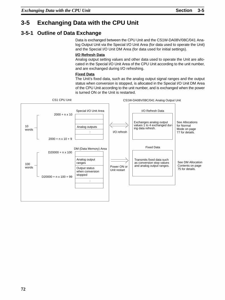
3-5SectionExchanging Data with the CPU Unit
72
3-5 Exchanging Data with the CPU Unit
3-5-1 Outline of Data ExchangeData is exchanged between the CPU Unit and the CS1W-DA08V/08C/041 Ana-log Output Unit via the Special I/O Unit Area (for data used to operate the Unit)and the Special I/O Unit DM Area (for data used for initial settings).
I/O Refresh DataAnalog output setting values and other data used to operate the Unit are allo-cated in the Special I/O Unit Area of the CPU Unit according to the unit number,and are exchanged during I/O refreshing.
Fixed DataThe Unit’s fixed data, such as the analog output signal ranges and the outputstatus when conversion is stopped, is allocated in the Special I/O Unit DM Areaof the CPU Unit according to the unit number, and is exchanged when the poweris turned ON or the Unit is restarted.
CS1 CPU Unit CS1W-DA08V/08C/041 Analog Output Unit
Special I/O Unit Area I/O Refresh Data
Analog outputs
DM (Data Memory) Area
Analog outputranges
Output statuswhen conversionstopped
I/O refresh
Power ON orUnit restart
Exchanges analog outputvalues 1 to 4 exchanged dur-ing data refresh.
See Allocationsfor NormalMode on page77 for details.
Transmits fixed data suchas conversion stop valuesand analog output ranges.
See DM AllocationContents on page75 for details.
2000 + n x 10
2000 + n x 10 + 9
D20000 + n x 100
D20000 + n x 100 + 99
10words
100words
Fixed Data
:
:

3-5SectionExchanging Data with the CPU Unit
73
3-5-2 Unit Number Settings
The Special I/O Unit Area and Special I/O Unit DM Area word addresses thateach Analog Output Unit occupies are set by the unit number switch on the frontpanel of the Unit.
Switchsetting
Unitnumber
Special/O Unit Areaaddresses
Special I/O Unit DM Areaaddresses
0 Unit #0 CIO 2000 to CIO 2009 D20000 to D20099
1 Unit #1 CIO 2010 to CIO 2019 D20100 to D20199
2 Unit #2 CIO 2020 to CIO 2029 D20200 to D20299
3 Unit #3 CIO 2030 to CIO 2039 D20300 to D20399
4 Unit #4 CIO 2040 to CIO 2049 D20400 to D20499
5 Unit #5 CIO 2050 to CIO 2059 D20500 to D20599
6 Unit #6 CIO 2060 to CIO 2069 D20600 to D20699
7 Unit #7 CIO 2070 to CIO 2079 D20700 to D20799
8 Unit #8 CIO 2080 to CIO 2089 D20800 to D20899
9 Unit #9 CIO 2090 to CIO 2099 D20900 to D20999
10 Unit #10 CIO 2100 to CIO 2109 D21000 to D21099
~ ~ ~ ~
n Unit #n CIO 2000 + (n x 10) toCIO 2000 + (n x 10) + 9
D20000 + (n x 100) to D20000 + (n x 100) + 99
~ ~ ~ ~
95 Unit #95 CIO 2950 to CIO 2959 D29500 to D29599
Note If two or more Special I/O Units are assigned the same unit number, an “UNITNo. DPL ERR” error (in the Programming Console) will be generated (A40113will turn ON) and the PC will not operate.
3-5-3 Special I/O Unit Restart Bits
To restart the Unit operations after changing the contents of the data memory orcorrecting an error, turn ON the power to the PC again or turn the Special I/O UnitRestart Bit ON and then OFF again.
Special I/OUnit Area word
address
Function
A50200 Unit No. 0 Restart Bit Restarts the Unit when turned
A50201 Unit No. 1 Restart Bit ON and then OFF again.
~ ~
A50215 Unit No. 15 Restart Bit
A50300 Unit No. 16 Restart Bit
~ ~
A50715 Unit No. 95 Restart Bit
Note If the error is not corrected by restarting the Unit or turning the Special I/O UnitRestart Bit ON and then OFF again, replace the Analog Output Unit.

3-5SectionExchanging Data with the CPU Unit
74
3-5-4 Fixed Data AllocationsThe initial settings of the Analog Output Unit are set according to the data allo-cated in the Special I/O Unit DM Area. Settings, such as the outputs used, andthe analog output signal ranges must be set in this area.
D(m+1)
D(m)
D20300 to D20399
D20400 to D20499
D20500 to D20599
D20000 to D20099
D20100 to D20199
D20200 to D20299
D20900 to D20999
D20600 to D20699
D20700 to D20799
D20800 to D20899
SYSMAC CS1-series PC CS1W-DA08V/08C/041 Analog Output Unit
(Fixed Data Area)
Unit #0
Unit #1
Unit #2
Unit #3
Unit #4
Unit #5
Unit #6
Unit #7
Unit #8
Unit #9
(Special I/O Unit DM Area)
Word
D29500 to D29599
D21000 to D21099
~
D20000 + (n x 100) toD20000 + (n x 100) + 99
Unit #10
~
Unit #n
~
Unit #95
D(m+2 tom+9)(See note.)
Outputs usedsetting
Output signalrange
Output holdfunction setting
Data is automaticallytransferred to each unitnumber when the poweris turned ON, or whenthe Special I/O UnitRestart Bit is turned ON.
m = 20000 + (100 x unit number)
~
Note D(m+5) for the CS1W-DA041.
Note 1. The Special I/O Unit DM Area words that are occupied by the Analog OutputUnit are set using the unit number switch on the front panel of the Unit. Referto 3-3-2 Unit Number Switch for details on the method used to set the unitnumber switch.
2. If two or more Special I/O Units are assigned the same unit number, an“UNIT No. DPL ERR” error (in the Programming Console) will be generated(A40113 will turn ON) and the PC will not operate.
DM Allocation andContents

3-5SectionExchanging Data with the CPU Unit
75
The following table shows the allocation of DM words and bits for both normaland adjustment mode.
CS1W-DA08V/08C
DM word Bits
15 14 13 12 11 10 9 8 7 6 5 4 3 2 1 0D(m) Not used. Output use setting
Out-put8
Out-put 7
Out-put 6
Out-put 5
Out-put 4
Out-put 3
Out-put 2
Out-put 1
D(m+1) Output signal range setting
Output 8 Output 7 Output 6 Output 5 Output 4 Output 3 Output 2 Output 1
D(m+2) Not used. Output 1: Output status when conversion stopped
D(m+3) Not used. Output 2: Output status when conversion stopped
D(m+4) Not used. Output 3: Output status when conversion stopped
D(m+5) Not used. Output 4: Output status when conversion stopped
D(m+6) Not used. Output 5: Output status when conversion stopped
D(m+7) Not used. Output 6: Output status when conversion stopped
D(m+8) Not used. Output 7: Output status when conversion stopped
D(m+9) Not used. Output 8: Output status when conversion stopped
CS1W-DA041
DM word Bits
15 14 13 12 11 10 9 8 7 6 5 4 3 2 1 0D(m) Not used. Not used. Output use setting
Out-put 4
Out-put 3
Out-put 2
Out-put 1
D(m+1) Not used. Output signal range setting
Output 4 Output 3 Output 2 Output 1
D(m+2) Not used. Output 1: Output status when conversion stopped
D(m+3) Not used. Output 2: Output status when conversion stopped
D(m+4) Not used. Output 3: Output status when conversion stopped
D(m+5) Not used. Output 4: Output status when conversion stopped
Note For the DM word addresses, m = 20000 + (100 x unit number).
Set Values and Stored Values
Item Contents Page
Output Use setting 0: Not used.1: Used.
75, 79
Output signal range 00: –10 to 10 V01: 0 to 10 V10: 1 to 5 V/4 to 20 mA (See note 1.)11: 0 to 5 V
75, 79
Output status when stopped 00: CLR Outputs 0 or minimum value of each range. (See note 2.)
01: HOLD Holds output just before stopping.02: MAX Outputs maximum value of range.
81
Note 1. With the CS1W-DA041, the output signal ranges 1 to 5 V and 4 to 20 mA areswitched using the output terminal connections. For details, refer to 3-4-3Output Wiring Example. With the CS1W-DA08C, these ranges are invalid.Regardless of the settings made, the output range will be 4 to 20 mA.
2. The values output for the signal ranges will be 0 V for the range of ±10 V, andthe minimum value for the other ranges. For details, refer to 3-6-3 OutputHold Function.
DM Allocation Contents

3-5SectionExchanging Data with the CPU Unit
76
3-5-5 I/O Refresh Data AllocationsI/O refresh data for the Analog Output Unit is exchanged according to the alloca-tions in the Special I/O Unit Area.
CIO n + 9
CIO n toCIO n + 8
CIO 2030 to CIO 2039
CIO 2040 to CIO 2049
CIO 2050 to CIO 2059
CIO 2000 to CIO 2009
CIO 2010 to CIO 2019
CIO 2020 to CIO 2029
CIO 2090 to CIO 2099
CIO 2060 to CIO 2069
CIO 2070 to CIO 2079
CIO 2080 to CIO 2089
SYSMAC CS1-series PC CS1W-DA08V/08C/041 Analog Output Unit
IN refresh
(I/O Refresh Data Area)
Unit #0
Unit #1
Unit #2
Unit #3
Unit #4
Unit #5
Unit #6
Unit #7
Unit #8
Unit #9
(Special I/O Unit Area)
At the I/O refresh by thePC, outputs (CPU toUnit) and inputs (Unit toCPU) are refreshed inorder with every cycle.
OUT refresh
Allocated words
CIO 2950 to CIO 2959
CIO 2100 to CIO 2109
~
CIO 2000 + (n x 10) toCIO 2000 + (n x 10) + 9
Unit #10
~
Unit #n
~
Unit #95
Normal mode
CIO n + 9
CIO n toCIO n + 7
IN refresh
OUT refresh
Adjustment mode
n = 2000 + (10 x unit number)
~
I/O refresh
Note 1. The Special I/O Unit Area words that are occupied by the Analog Output Unitare set using the unit number switch on the front panel of the Unit. Refer to3-3-2 Unit Number Switch for details on the method used to set the unit num-ber switch.
2. If two or more Special I/O Units are assigned the same unit number, an“UNIT No. DPL ERR” error (in the Programming Console) will be generated(A40113 will turn ON) and the PC will not operate.

3-5SectionExchanging Data with the CPU Unit
77
For normal mode, set the operation mode switch on the rear panel of the Unit as
shown in the following diagram.
The allocation of words and bits in the CIO Area is shown in the following table.
CS1W-DA08V/08C
I/O Word Bits
15 14 13 12 11 10 9 8 7 6 5 4 3 2 1 0
Output n Not used. Conversion enable(CPU toUnit)
Out-put 8
Out-put 7
Out-put 6
Out-put 5
Out-put 4
Out-put 3
Out-put 2
Out-put 1Unit)
n + 1 Output 1 set value
163 162 161 160
n + 2 Output 2 set value
n + 3 Output 3 set value
n + 4 Output 4 set value
n + 5 Output 5 set value
n + 6 Output 6 set value
n + 7 Output 7 set value
n + 8 Output 8 set value
Input n + 9 Alarm Flags Output setting error(Unit toCPU)
Out-put 8
Out-put 7
Out-put 6
Out-put 5
Out-put 4
Out-put 3
Out-put 2
Out-put 1
CS1W-DA041
I/O Word Bits
15 14 13 12 11 10 9 8 7 6 5 4 3 2 1 0
Output n Not used. Not used. Conversion enable(CPU toUnit)
Out-put 4
Out-put 3
Out-put 2
Out-put 1Unit)
n + 1 Output 1 set value
163 162 161 160
n + 2 Output 2 set value
n + 3 Output 3 set value
n + 4 Output 4 set value
n + 5 Not used.
n + 6 Not used.
n + 7 Not used.
n + 8 Not used.
Input n + 9 Alarm Flags Not used. Output setting error(Unit toCPU)
Out-put 4
Out-put 3
Out-put 2
Out-put 1
Allocations for NormalMode

3-5SectionExchanging Data with the CPU Unit
78
Set Values and Stored ValuesI/O Item Contents Page
Output Conversion enable 0: Conversion output stopped.1: Conversion output begun.
81
Set value 16-bit binary data 80
Output setting error 0: No error1: Output setting error
83
Common Alarm Flags Bits 00 to 03: Output set value errorBits 04 to 09: Not usedBit 10: Output hold setting error Bit 11: Not usedBit 15: Operating in adjustment mode
(always 0 in normal mode)
77, 95
Note For the CIO word addresses, n = 2000 + 10 x unit number.
For adjustment mode, set the operation mode switch on the rear panel of theUnit as shown in the following diagram. When the Unit is set for adjustmentmode, the ADJ indicator on the front panel of the Unit will flash.
The allocation of CIO words and bits is shown in the following table.
I/O Word Bits
15 14 13 12 11 10 9 8 7 6 5 4 3 2 1 0Output n Not used. Outputs to be adjusted(CPU to 161 160Unit)
n + 1 Not used. Not used. Clr Set Up Down Gain Off-set
n + 2 Not used.
n + 3 Not used.
n + 4 Not used.
n + 5 Not used.
n + 6 Not used.
n + 7 Not used.
Input n + 8 Conversion value or set value at time of adjustment(Unit toCPU) 163 162 161 160
n + 9 Alarm Flags Not used.
Allocation forAdjustment Mode

3-6SectionAnalog Output Functions and Operating Procedures
79
Refer to 3-7 Adjusting Offset and Gain or 3-8-2 Alarms Occurring at the AnalogOutput Unit for further details.
Item Contents
Output to be adjusted Sets output to be adjusted.Leftmost digit: 1 (output)Rightmost digit: 1 to 8 (1 to 4 for CS1W-DA041)
Offset (Offset Bit) When ON, adjusts offset deviation.
Gain (Gain Bit) When ON, adjusts gain deviation.
Down (Down Bit) Decrements the adjustment value while ON.
Up (Up Bit) Increments the adjustment value while ON.
Set (Set Bit) Sets adjusted value and writes to EEPROM.
Clr (Clear Bit) Clears adjusted value. (Returns to default status)
Conversion value foradjustment
The conversion value for adjustment is stored as 16bits of binary data.
Alarm Flags Bit 12: Not usedBit 13: Output number setting error (in adjustmentmode)Bit 14: EEPROM write error (in adjustment mode)Bit 15: Operating in adjustment mode
(always 1 in adjustment mode)
Note For the CIO word addresses, n = 2000 + (10 x unit number).
3-6 Analog Output Functions and Operating Procedures
3-6-1 Output Settings and Conversions
The Analog Output Unit converts only analog outputs specified by output num-bers 1 to 8 (output numbers 1 to 4 for CS1W-DA041). To specify the analog out-puts to be used, turn ON from a Programming Device the D(m) bits in the DMArea shown in the following diagram.
15 14 13 12 11 10 09 08 07 06 05 04 03 02 01 00Bit
D(m)O
utpu
t 2
Out
put 1
0: Not used1: Used
Out
put 4
Out
put 3
Out
put 6
Out
put 5
Out
put 8
Out
put 7
Note There are only four outputs for the CS1W-DA041.
The analog output conversion cycle can be shortened by setting any unusedoutput numbers to 0.
Conversion cycle = (1 ms) x (Number of outputs used)
Note 1. For the DM word addresses, m = 20000 + (100 x unit number).
2. Output numbers not used (set to 0) will be output at 0 V.
Set Values and StoredValues
Output Numbers

3-6SectionAnalog Output Functions and Operating Procedures
80
Any of four types of output signal range (–10 to 10 V, 0 to 10 V, 1 to 5 V, and 0 to5 V) can be selected for each of the outputs. To specify the output signal rangefor each output, use a Programming Device to set the D(m+1) bits in the DMArea shown in the following diagram.
15 14 13 12 11 10 09 08 07 06 05 04 03 02 01 00Bit
D(m + 1)
Out
put 2
Out
put 1
00: -10 to 10 V01: 0 to 10 V10: 1 to 5 V11: 0 to 5 V
Out
put 4
Out
put 3
Out
put 6
Out
put 5
Out
put 8
Out
put 7
Note 1. For the DM word addresses, m = 20000 + (100 x unit number).
2. With the CS1W-DA041, the 1 to 5 V output range and the 4 to 20 mA outputrange are switched by changing the terminal connections.
3. There is no 4 to 20 mA output range for the CS1W-DA08V.
4. Output setting range settings for the CS1W-DA08C are invalid. The outputsignal range will be 4 to 20 mA, regardless of the settings.
5. When data memory settings have been carried out using a ProgrammingDevice, be sure to either turn the power supply for the PC OFF and then ONagain, or set the Special I/O Unit Restart Bit to ON. The contents of the datamemory settings will be transferred to the Special I/O Unit when the power isturned ON or the Special I/O Unit Restart Bit is ON.
Analog output set values are written to CIO words (n+1) to (n+8). For theCS1W-DA041, they are written to CIO words (n+1) to (n+4).
Word Function Stored value
n+1 Output 1 set value 16-bit binary data
n+2 Output 2 set value
n+3 Output 3 set value
n+4 Output 4 set value
n+5 Output 5 set value
n+6 Output 6 set value
n+7 Output 7 set value
n+8 Output 8 set value
For the CIO word addresses, n = 2000 + (10 x unit number).
Use MOV(021) or XFER(070) to write values in the user program.
In this example, the set value from only one output is written. (The unit number is0.)
MOV (021)
D00001
2001
Input conditionThe set value stored in D 00001is written to CIO word 2001 (out-put number 1).
Output Signal Range
Writing Set Values
Example 1
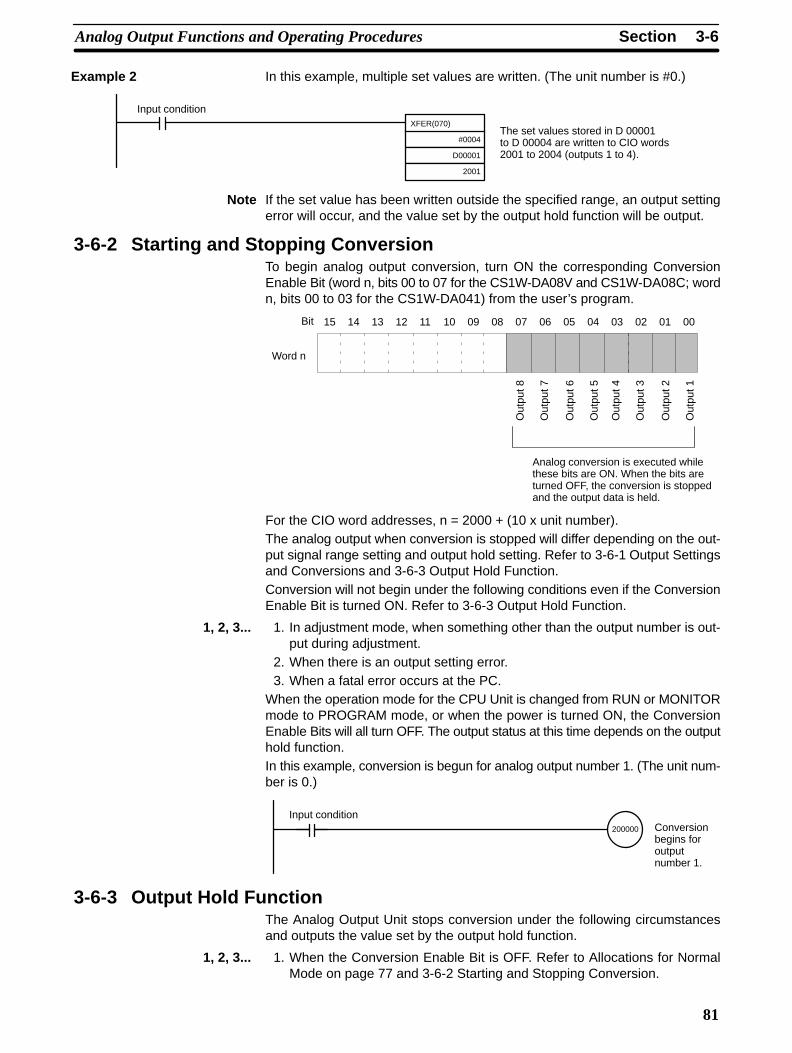
3-6SectionAnalog Output Functions and Operating Procedures
81
In this example, multiple set values are written. (The unit number is #0.)
XFER(070)
#0004
D00001
2001
Input condition
The set values stored in D 00001to D 00004 are written to CIO words2001 to 2004 (outputs 1 to 4).
Note If the set value has been written outside the specified range, an output settingerror will occur, and the value set by the output hold function will be output.
3-6-2 Starting and Stopping ConversionTo begin analog output conversion, turn ON the corresponding ConversionEnable Bit (word n, bits 00 to 07 for the CS1W-DA08V and CS1W-DA08C; wordn, bits 00 to 03 for the CS1W-DA041) from the user’s program.
15 14 13 12 11 10 09 08 07 06 05 04 03 02 01 00Bit
Out
put 2
Out
put 1
Analog conversion is executed whilethese bits are ON. When the bits areturned OFF, the conversion is stoppedand the output data is held.
Word n
Out
put 4
Out
put 3
Out
put 6
Out
put 5
Out
put 8
Out
put 7
For the CIO word addresses, n = 2000 + (10 x unit number).The analog output when conversion is stopped will differ depending on the out-put signal range setting and output hold setting. Refer to 3-6-1 Output Settingsand Conversions and 3-6-3 Output Hold Function.Conversion will not begin under the following conditions even if the ConversionEnable Bit is turned ON. Refer to 3-6-3 Output Hold Function.
1, 2, 3... 1. In adjustment mode, when something other than the output number is out-put during adjustment.
2. When there is an output setting error.3. When a fatal error occurs at the PC.
When the operation mode for the CPU Unit is changed from RUN or MONITORmode to PROGRAM mode, or when the power is turned ON, the ConversionEnable Bits will all turn OFF. The output status at this time depends on the outputhold function.In this example, conversion is begun for analog output number 1. (The unit num-ber is 0.)
200000
Input conditionConversionbegins foroutputnumber 1.
3-6-3 Output Hold FunctionThe Analog Output Unit stops conversion under the following circumstancesand outputs the value set by the output hold function.
1, 2, 3... 1. When the Conversion Enable Bit is OFF. Refer to Allocations for NormalMode on page 77 and 3-6-2 Starting and Stopping Conversion.
Example 2

3-6SectionAnalog Output Functions and Operating Procedures
82
2. In adjustment mode, when something other than the output number is out-put during adjustment. Refer to Allocation for Adjustment Mode on page 78.
3. When there is an output setting error. Refer to Allocations for Normal Modeon page 77 and 3-6-4 Output Setting Errors.
4. When a fatal error occurs at the PC.
5. When there is an I/O bus error.
6. When the CPU Unit is in LOAD OFF status.
7. When there is a WDT (watchdog timer) error in the CPU Unit.
CLR, HOLD, or MAX can be selected for the output status when conversion isstopped.
Output signalrange
CLR HOLD MAX
0 to 10 V –0.5 V (Min.–5%of full scale)
Voltage that was outputjust prior to stop.
10.5 V (Max.+5%of full scale)
–10 to 10 V 0.0 V Voltage that was outputjust prior to stop.
11.0 V (Max.+5%of full scale)
1 to 5 V 0.8 V (Min.–5% offull scale)
Voltage that was outputjust prior to stop.
5.2 V (Max.+5% offull scale)
0 to 5 V –0.25 V (Min.–5%of full scale)
Voltage that was outputjust prior to stop.
5.25 V (Max.+5%of full scale)
4 to 20 mA 3.2 mA (Min. –5%of full scale)
Current that was outputjust prior to stop.
20.8 mA(Max.+5% of fullscale)
The above values may fluctuate if offset/gain adjustment has been applied.
To specify the output hold function, use a Programming Device to set the DMArea words D(m+2) to D(m+9) as shown in the following table. (DM Area wordsD(m+2) to D(m+5)for the CS1W-DA041.)
DM word Function Set value
D(m+2) Output 1: Output status when conversionis stopped
xx00: CLROutput 0 or
D(m+3) Output 2: Output status when conversionis stopped
minimum value ofrange (–5%).
D(m+4) Output 3: Output status when conversionis stopped
xx01: HOLDHold output value
D(m+5) Output 4: Output status when conversionis stopped
prior to stop.
xx02: MAX
D(m+6) Output 5: Output status when conversionis stopped
Output maximumvalue of range
D(m+7) Output 6: Output status when conversionis stopped
(105%).
Set any value in the
D(m+8) Output 7: Output status when conversionis stopped
leftmost bytes (xx).
D(m+9) Output 8: Output status when conversionis stopped
For the DM word addresses, m = 20000 + (100 x unit number).
Note After specifying the DM settings from a Programming Device, it will be neces-sary to either power up the PC again or turn ON the Special I/O Unit Restart Bit totransfer the contents of the DM settings to the Special I/O Unit.

3-6SectionAnalog Output Functions and Operating Procedures
83
3-6-4 Output Setting ErrorsIf the analog output set value is greater than the specified range, a setting errorsignal will be stored in CIO word n+9, bits 00 to 07. (Bits 00 to 03 for theCS1W-DA041.)
15 14 13 12 11 10 09 08 07 06 05 04 03 02 01 00Bit
Out
put 2
Out
put 1
Word n+9
When a setting error is detectedfor a particular output, the corre-sponding bit turns ON. When theerror is cleared, the bit turns OFF.
Out
put 4
Out
put 3
Out
put 6
Out
put 5
Out
put 8
Out
put 7
For the CIO word addresses, n = 2000 + (10 x unit number).
The voltage for an output number at which a setting error has occurred will beoutput according to the output hold function.

3-7SectionAdjusting Offset and Gain
84
3-7 Adjusting Offset and Gain
3-7-1 Adjustment Mode Operational FlowThe adjustment mode enables the output of the connected devices to be cali-brated.
This function adjusts the output voltage according to the offset value and gainvalue at the input device, and sets the settings values at the Unit at that time to0000 and 0FA0 (07D0 if the range is ±10 V) respectively.
For example, suppose that the specifications range for the external input device(e.g., indicator, etc.) is 100.0 to 500.0 when using in the range 1 to 5 V. Also, sup-pose that when voltage is output at the Analog Output Unit at a set value of 0000,the external input device actually displays 100.5 and not 100.0. It is possible tomake settings to adjust the output voltage (making it smaller in this case) so that100.0 is displayed and to make 0000 (not FFFB as in this case) the set value forwhich 100.0 is displayed.
Similarly for gain values, suppose that when voltage is output at the Analog Out-put Unit at a set value of 0FA0, the external input device actually displays 500.5and not 500.0. It is possible to make settings to adjust the output voltage (make itsmaller in this case) so that 500.0 is displayed and to make 0FA0 (not 0F9B as inthis case) the set value for which 500.0 is displayed.
External input devicedisplay
Set value beforeadjustment (word n+8)
Set value afteradjustment
100.0 FFFB 0000
500.0 0F9B 0FA0

!
!
3-7SectionAdjusting Offset and Gain
85
The following diagram shows the flow of operations when using the adjustmentmode for adjusting offset and gain.
Change the operation mode switch on the rear panel of the Unit.
Turn ON the PC.
When adjusting another output number
When adjusting the same output number
Set the output number.
Offset adjustment
Offset Bit ON (Bit 0 of CIO wordn+1 turns ON.)
Set Bit ON (Bit 4 of CIO wordn+1 turns ON.)
Turn OFF power to the PC.
Change the operation mode switch on the rear panel of the Unit.
Set the operation mode switch to normal mode.
Set the operation mode switch to adjustment mode.
The ADJ indicator will flash while in adjustment mode.
Start up the PC in PROGRAM mode.
Write the output number to be adjustedin the rightmost byte of CIO word n.
Gain adjustment
Gain Bit ON (Bit 1 of CIO wordn+1 turns ON.)
Adjustmentvalue setting
(Bits 2 and 3 ofCIO word n+1turn ON.)
Output adjustment
Set Bit ON (Bit 4 of CIO wordn+1 turns ON.)
Adjustmentvalue setting
(Bits 2 and 3 ofCIO word n+1turn ON.)
Output adjustment
Caution Be sure to turn OFF the power to the PC before changing the setting of theoperation mode switch.
Caution Set the PC to PROGRAM mode when using the Analog Output Unit in adjust-ment mode. If the PC is in MONITOR mode or RUN mode, the Analog OutputUnit will stop operating, and the output values that existed immediately beforethis stoppage will be retained.

!
3-7SectionAdjusting Offset and Gain
86
Caution Always perform adjustments in conjunction with offset and gain adjustments.
3-7-2 Output Offset and Gain Adjustment ProceduresTo specify the output number to be adjusted, write the value to the rightmost byteof CIO word n as shown in the following diagram.
(Rightmost)(Leftmost)
Word n
Output to be adjusted (1 to 8)(1 to 4 for CS1W-DA041)
I/O specification1: Output (fixed)
For the CIO word addresses, n = 2000 + 10 x unit number.
The following example uses output number 1 adjustment for illustration. (Theunit number is 0.)
CLR
SHIFTCH
*DM2
C0
A0
A0
AMON
CHG
1B
1B
WRITE
The CIO word n+1 bits shown in the following diagram are used for adjustingoffset and gain.
15 14 13 12 11 10 09 08 07 06 05 04 03 02 01 00Bit
Word n+1
Cle
ar B
it
Set
Bit
Gai
n B
it
Offs
et B
it
Up
Bit
Dow
n B
it
Specifying OutputNumber to be Adjusted
Bits Used for AdjustingOffset and Gain

3-7SectionAdjusting Offset and Gain
87
The procedure for adjusting the analog output offset is explained below. Asshown in the following diagram, the set value is adjusted so that the analog out-put reaches the standard value (0V/1V).
10 V
00FA0
Offset adjustment output range
Output signal range:0 to 10 V
The following example uses output number 1 adjustment for illustration. (Theunit number is 0.)
1, 2, 3... 1. Turn ON bit 00 (the Offset Bit) of CIO word n+1. (Hold the ON status.)
CLR
SHIFTCONT
#2
C0
A0
A1
B0
A0
AMON
SET
2. Check whether the output devices are connected.
Voltage output/current output
Output 1
CS1W-DA08V/08CCS1W-DA041 (voltage output)
Current output
CS1W-DA041 (current output)
3. Monitor CIO word n+8 and check the set value while the Offset Bit is ON.
CLR
SHIFTCH
*DM2
C0
A0
A8 MON
Offset Adjustment

3-7SectionAdjusting Offset and Gain
88
4. Change the set value so that the output voltage are as shown in the followingtable. The data can be set within the indicated ranges.
Output signal range Possible outputvoltage/current
adjustment
Output range
0 to 10 V –0.5 to 0.5 V FF38 to 00C8
–10 to 10 V –1.0 to 1.0 V
1 to 5 V 0.8 to 1.2 V
0 to 5 V –0.25 to 0.25 V
Change the set value, using the Up Bit (bit 03 of word n+1) and the Down Bit(bit 02 of word n+1).
15 14 13 12 11 10 09 08 07 06 05 04 03 02 01 00Bit
Up Bit Down Bit
While the Down Bit is ON, the set value will bedecreased by 1 resolution every 0.5 seconds.After it has been ON for 3 seconds, the setvalue will be decreased by 1 resolution every0.1 seconds.
Word n+1
While the Up Bit is ON, the set value will beincreased by 1 resolution every 0.5 seconds.After it has been ON for 3 seconds, the setvalue will be increased by 1 resolution every0.1 seconds.
• The following example increases the output voltage.
SHIFTCONT
#2
C0
A0
A1
B0
A3
DMON
The bit will remain ON until the output becomes an appropriate value, atwhich time, it will turn OFF.
SET
RESET
• The following example decreases the output voltage.
SHIFTCONT
#2
C0
A0
A1
B0
A2
CMON

!
!
3-7SectionAdjusting Offset and Gain
89
The bit will remain ON until the output becomes an appropriate value, atwhich time, it will turn OFF.
SET
RESET
5. Check the 0-V/1-V output, and then turn bit 04 (the Set Bit) of CIO word n+1ON and then OFF again.
SHIFTCONT
#2
C0
A0
A1
B0
A4
EMON
SET
RESET
While the Offset Bit is ON, the offset value will be saved to the Unit’sEEPROM when the Set Bit turns ON.
6. To finish the offset adjustment, turn OFF bit 00 (the Offset Bit) of CIO wordn+1.
SHIFTCONT
#2
C0
A0
A1
B0
A0
AMON
SET
Caution Do not turn OFF the power supply or restart the Unit while the Set Bit is ON (datais being written to the EEPROM). Otherwise, illegal data may be written in theUnit’s EEPROM and “EEPROM Errors” may occur when the power supply isturned ON or when the Unit is restarted, causing a malfunction.
Caution When making adjustments, be sure to perform both the offset adjustment andgain adjustment at the same time.
Note The EEPROM can be overwritten 50,000 times.

3-7SectionAdjusting Offset and Gain
90
The procedure for adjusting the analog output gain is explained below. As shownin the following diagram, the set value is adjusted so that the analog output ismaximized (to 10V/5V).
10 V
00FA0
Output signal range:0 to 10 V
Gain adjustment output range
The following example uses output number 1 adjustment for illustration. (Theunit number is 0.)
1, 2, 3... 1. Turn ON bit 01 (the Gain Bit) of CIO word n+1. (Hold the ON status.)
CLR
SHIFTCONT
#2
C0
A0
A1
B0
A1
BMON
SET
2. Check whether the output devices are connected.
Voltage output/current output
Output 1
CS1W-DA08V/08CCS1W-DA041 (voltage output)
Current output
CS1W-DA041 (current output)
3. Monitor CIO word n+8 and check the set value while the Gain Bit is ON.
CLR
SHIFTCH
*DM2
C0
A0
A8 MON
Gain Adjustment

3-7SectionAdjusting Offset and Gain
91
4. Change the set value so that the output voltage is as shown in the followingtable. The data can be set within the indicated ranges.
Output signal range Possible outputvoltage/current
adjustment
Output range
0 to 10 V 9.5 to 10.5 V 0ED8 to 1068
–10 to 10 V 9 to 11 V 0708 to 0898
1 to 5 V 4.8 to 5.2 V 0ED8 to 1068
0 to 5 V 4.75 to 5.25 V 0ED8 to 1068
Change the set value, using the Up Bit (bit 03 of word n+1) and the Down Bit(bit 02 of word n+1).
15 14 13 12 11 10 09 08 07 06 05 04 03 02 01 00Bit
Up Bit Down Bit
While the Up Bit is ON, the set value will beincreased by 1 resolution every 0.5 seconds.After it has been ON for 3 seconds, the setvalue will be increased by 1 resolution every0.1 seconds.
While the Down Bit is ON, the set value will bedecreased by 1 resolution every 0.5 seconds.After it has been ON for 3 seconds, the setvalue will be decreased by 1 resolution every0.1 seconds.
Word n+1
• The following example increases the output voltage.
SHIFTCONT
#2
C0
A0
A1
B0
A3
DMON
The bit will remain ON until the output voltage becomes an appropriatevalue, at which time, the output will turn OFF.
SET
RESET
• The following example decreases the output voltage.
SHIFTCONT
#2
C0
A0
A1
B0
A2
CMON

!
!
3-7SectionAdjusting Offset and Gain
92
The bit will remain ON until the output voltage becomes an appropriatevalue, at which time, the output will turn OFF.
SET
RESET
5. Check the 10V/5V output, and then turn bit 04 (the Set Bit) of CIO word n+1ON and then OFF again.
SHIFTCONT
#2
C0
A0
A1
B0
A4
EMON
SET
RESET
While the Gain Bit is ON, the gain value will be saved to the Unit’s EEPROMwhen the Set Bit turns ON.
6. To finish the gain adjustment, turn OFF bit 01 (the Gain Bit) of CIO word n+1.
SHIFTCONT
#2
C0
A0
A1
B0
A1
BMON
RESET
Caution Do not turn OFF the power supply or restart the Unit while the Set Bit is ON (datais being written to the EEPROM). Otherwise, illegal data may be written in theUnit’s EEPROM and “EEPROM Errors” may occur when the power supply isturned ON or when the Unit is restarted, causing a malfunction.
Caution When making adjustments, be sure to perform both the offset adjustment andgain adjustment at the same time.
Note The EEPROM can be overwritten 50,000 times.

!
3-7SectionAdjusting Offset and Gain
93
Follow the procedure outlined below to return the offset and gain adjusted val-ues to their default settings.
The following example uses output number 1 adjustment for illustration. (Theunit number is 0.)
1, 2, 3... 1. Turn ON bit 05 (the Clear Bit) of CIO word n+1. (Hold the ON status.)Regardless of the set value, 0000 will be monitored in CIO word n+8.
SHIFTCONT
#2
C0
A0
A1
B0
A5
FMON
SET
2. Turn bit 04 of CIO word n+1 ON and then OFF again.
SHIFTCONT
#2
C0
A0
A1
B0
A4
EMON
SET
RESET
While the Clear Bit is ON, the adjusted value will be cleared and reset to thedefault offset and gain values when the Set Bit turns ON.
3. To finish the clearing of adjusted values, turn OFF bit 05 (the Clear Bit) ofCIO word n+1.
SHIFTCONT
#2
C0
A0
A1
B0
A5
FMON
RESET
Caution Do not turn OFF the power supply or restart the Unit while the Set Bit is ON (datais being written to the EEPROM). Otherwise, illegal data may be written in theUnit’s EEPROM and “EEPROM Errors” may occur when the power supply isturned ON or when the Unit is restarted, causing a malfunction.
Note The EEPROM can be overwritten 50,000 times.
Clearing Offset and GainAdjusted Values

3-8SectionHandling Errors and Alarms
94
3-8 Handling Errors and Alarms
3-8-1 Indicators and Error Flowchart
If an alarm or error occurs in the Analog Output Unit, the ERC or ERH indicatorson the front panel of the Unit will light.
Front panel of Unit
RUN
ERC
ADJ
ERH
LED Meaning Indicator Operating statusRUN Operating Lit Operating in normal mode.(green) Not lit Unit has stopped exchanging data with
the CPU Unit.ERC (red) Unit has
detected anerror
Lit Alarm has occurred (such asdisconnection detection) or initialsettings are incorrect.
Not lit Operating normally.
ADJ(yellow)
Adjusting Flashing Operating in offset/gain adjustmentmode.
Not lit Other than the above.
ERH (red) Error in theCPU Unit
Lit Error has occurred during dataexchange with the CPU Unit.
Not lit Operating normally.
Use the following procedure for troubleshooting Analog Output Unit errors.
Error occurs.
Is the ERC indicatorlit?
Refer to 3-8-5Troubleshooting.
Yes
No
Is the RUN indicatorlit?
Yes
No
Alarm has occurred at the Analog Output Unit.(Refer to 3-8-2 Alarms Occurring at the Analog OutputUnit.)
Check whether the initial settings for the Analog OutputUnit are set correctly. (Refer to 3-8-2 Alarms Occurring atthe Analog Output Unit.)
Is the ERH indicatorlit?
Yes
No
Is the RUN indicatorlit?
Yes
No
Error detected by CPU Unit(Refer to 2-8-3 Errors in the CPU Unit.)
Check whether the unit number is set correctly. (Refer to 2-8-3 Errors in the CPU Unit.)
Indicators
TroubleshootingProcedure
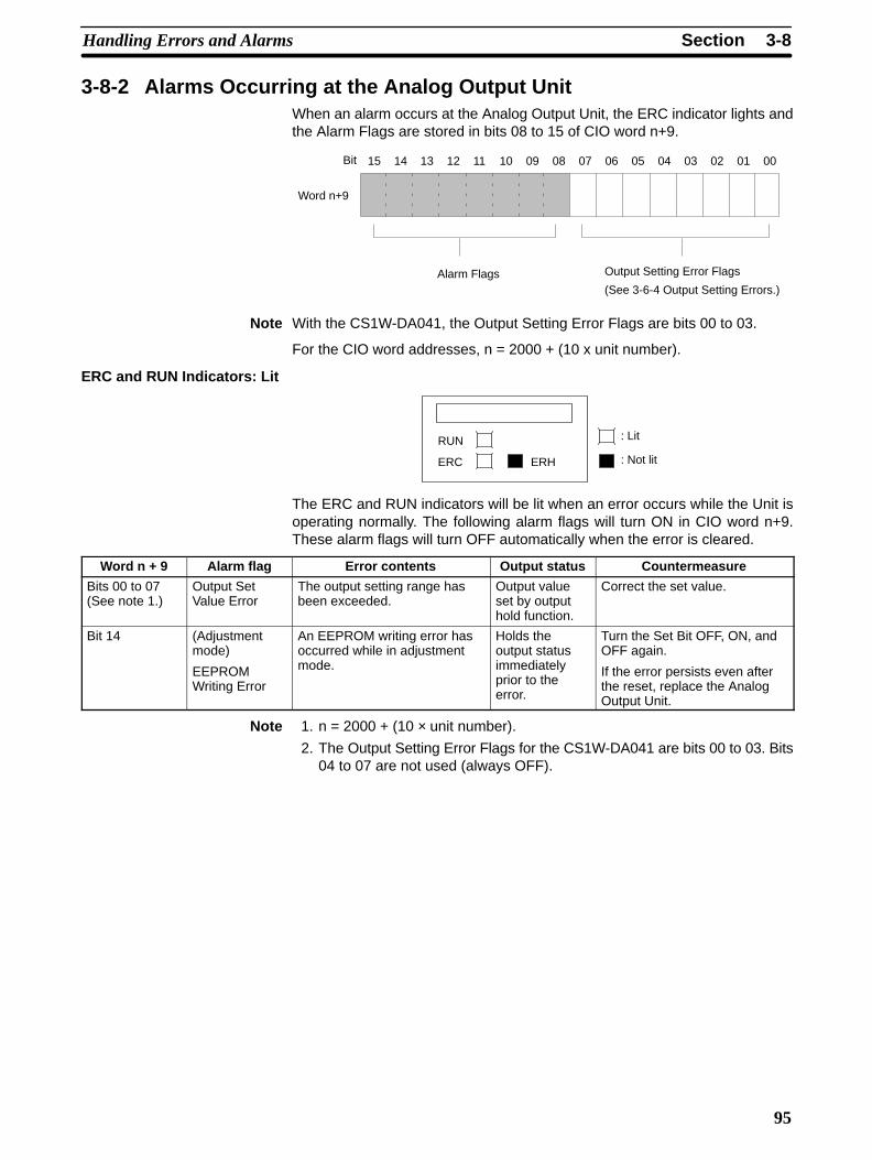
3-8SectionHandling Errors and Alarms
95
3-8-2 Alarms Occurring at the Analog Output UnitWhen an alarm occurs at the Analog Output Unit, the ERC indicator lights andthe Alarm Flags are stored in bits 08 to 15 of CIO word n+9.
15 14 13 12 11 10 09 08 07 06 05 04 03 02 01 00Bit
Word n+9
Output Setting Error Flags
(See 3-6-4 Output Setting Errors.)Alarm Flags
Note With the CS1W-DA041, the Output Setting Error Flags are bits 00 to 03.
For the CIO word addresses, n = 2000 + (10 x unit number).
ERC and RUN Indicators: Lit
RUN
ERC ERH
: Lit
: Not lit
The ERC and RUN indicators will be lit when an error occurs while the Unit isoperating normally. The following alarm flags will turn ON in CIO word n+9.These alarm flags will turn OFF automatically when the error is cleared.
Word n + 9 Alarm flag Error contents Output status Countermeasure
Bits 00 to 07(See note 1.)
Output SetValue Error
The output setting range hasbeen exceeded.
Output valueset by outputhold function.
Correct the set value.
Bit 14 (Adjustmentmode)
EEPROMWriting Error
An EEPROM writing error hasoccurred while in adjustmentmode.
Holds theoutput statusimmediatelyprior to theerror.
Turn the Set Bit OFF, ON, andOFF again.
If the error persists even afterthe reset, replace the AnalogOutput Unit.
Note 1. n = 2000 + (10 × unit number).
2. The Output Setting Error Flags for the CS1W-DA041 are bits 00 to 03. Bits04 to 07 are not used (always OFF).

3-8SectionHandling Errors and Alarms
96
ERC Indicator and RUN Indicator: Lit, ADJ Indicator: Flashing
RUN
ERC ERH
ADJ
: Lit
: Flashing
: Not lit
This alarm will occur in the case of incorrect operation while in the adjustmentmode. In adjustment mode, the Adjustment Mode ON Flag will turn ON in bit 15of CIO word n+9.
Word n + 9 Alarm flag Error contents Output status Countermeasure
Bit 13 (Adjustmentmode)
Output NumberSetting Error
In adjustment mode,adjustment cannot beperformed because thespecified output number is notset for use or because thewrong output number isspecified.
The outputvoltage orcurrentbecomes 0 V or0 mA.
Check whether the word noutput number to be adjusted isset from 11 to 14.
Check whether the outputnumber to be adjusted is set foruse by means of the DMsetting.
Bit 15 only ON (AdjustmentMode)
PC Error
The PC is in either MONITORor RUN mode while the AnalogOutput Unit is operating inadjustment mode.
The outputvoltage orcurrentbecomes 0 V or0 mA.
Detach the Unit. Switch therear panel DIP switch pin toOFF. Restart the Unit in normalmode.
Note When a PC error occurs in the adjustment mode, Unit operations will stop oper-ating. (The input and output values immediately prior to the error will be held.)
ERC Indicator: Lit, RUN Indicator: Not Lit
RUN
ERC ERH
: Lit
: Not lit
The ERC indicator will be lit when the initial settings for the Analog Output Unitare not set correctly. The alarm flags for the following errors will turn ON in CIOword n+9. These alarm flags will turn OFF when the error is cleared and the Unitis restarted, or the Special I/O Unit Restart Bit is turned ON and then OFF again.
Word n + 9 Alarm flag Error contents Countermeasure
Bit 10 Output HoldSetting Error
The wrong output status for whenconversion is stopped has beenspecified.
Specify a number from 0000 to 0002.
Note Bit 15 is normally turned OFF (i.e., set to 0).
3-8-3 Errors in the CPU UnitWhen errors occur in the CPU Unit or I/O bus, and I/O refresh with the Special I/OUnit is not performed correctly resulting in the Analog Output Unit malfunction-ing, the ERH indicator will be lit.
ERH and RUN Indicators: Lit
RUN
ERC ERH
: Lit
: Not lit

3-8SectionHandling Errors and Alarms
97
The ERH and RUN indicators will be lit if an error occurs in the I/O bus causing aWDT (watchdog timer) error in the CPU Unit, resulting in incorrect I/O refreshwith the Analog Output Unit.
Turn ON the power supply again or restart the system.For further details, refer to CS1-series CS1G/H-CPU-E ProgrammableControllers Operation Manual (W339).
Error Error contents Output condition
I/O bus error Error has occurred during dataexchange with the CPU Unit.
Depends on the output holdfunction.
CPU Unit monitoring error (seenote)
No response from CPU Unitduring fixed period.
Maintains the condition justbefore the error.
CPU Unit WDT error Error has been generated inCPU Unit.
Depends on the output holdfunction.
Note No error will be detected by the CPU Unit or displayed on the Programming Con-sole, because the CPU Unit is continuing operation.
ERH Indicator: Lit, RUN Indicator: Not Lit
RUN
ERC ERH
: Lit
: Not lit
The unit number for the Analog Output Unit has not been set correctly.
Error Error contents Output condition
Duplicate Unit Number The same unit number has beenassigned to more than one Unitor the unit number was set to avalue other than 00 to 95.
The output value will be 0 V.
Special I/O Unit Setting Error The Special I/O Units registeredin the I/O table are different fromthe ones actually mounted.
3-8-4 Restarting Special I/O UnitsThere are two ways to restart Special I/O Unit operation after having changedDM contents or having cleared the cause of an error. The first way is to power upthe PC again, and the second way is to turn the Special I/O Unit Restart Bit ONand then OFF again.
Special I/O Unit Restart Bits
Bits Functions
A50200 Unit #0 Restart Bit Turning the Restart Bit for any
A50201 Unit #1 Restart Bit Unit ON and then OFF again
~ ~restarts that Unit.
A50215 Unit #15 Restart Bit
A50300 Unit #16 Restart Bit
~ ~
A50715 Unit #95 Restart Bit
The output becomes 0 V or 0 mA during restart.
If the error is not cleared even after turning the Special I/O Unit Restart Bit ONand then OFF again, then replace the Unit.

3-8SectionHandling Errors and Alarms
98
3-8-5 TroubleshootingThe following tables explain the probable causes of troubles that may occur, andthe countermeasures for dealing with them.
Probable Cause Countermeasure Page
The output is not set for beingused.
Set the output for being used. 79
The output hold function is inoperation.
Turn ON the Output ConversionEnable Bit.
81
The conversion value is set outsideof the permissible range.
Set the data within the range. 58
Probable Cause Countermeasure Page
The output signal range setting iswrong.
Correct the output signal rangesetting.
80
The specifications of the outputdevice do not match those of theAnalog Output Unit (e.g., inputsignal range, input impedance).
Change the output device. 57
The offset or gain is not adjusted. Adjust the offset or gain. 84
Probable Cause Countermeasure Page
The output signals are beingaffected by external noise.
Try changing the shielded cableconnection (e.g., the grounding atthe output device).
71
Analog Output Does NotChange
Output Does Not Changeas Intended
Outputs are Inconsistent

99
SECTION 4Analog I/O Unit
This section explains how to use the CS1W-MAD44 Analog I/O Unit.
4-1 Specifications 100. . . . . . . . . . . . . . . . . . . . . . . . . . . . . . . . . . . . . . . . . . . . . . . . . . . . . . . . . . . . 4-1-1 Specifications 100. . . . . . . . . . . . . . . . . . . . . . . . . . . . . . . . . . . . . . . . . . . . . . . . . . . . . 4-1-2 I/O Function Block Diagram 102. . . . . . . . . . . . . . . . . . . . . . . . . . . . . . . . . . . . . . . . . 4-1-3 Input Specifications 103. . . . . . . . . . . . . . . . . . . . . . . . . . . . . . . . . . . . . . . . . . . . . . . . 4-1-4 Output Specifications 105. . . . . . . . . . . . . . . . . . . . . . . . . . . . . . . . . . . . . . . . . . . . . . .
4-2 Operating Procedure 107. . . . . . . . . . . . . . . . . . . . . . . . . . . . . . . . . . . . . . . . . . . . . . . . . . . . . . . 4-2-1 Procedure Examples 108. . . . . . . . . . . . . . . . . . . . . . . . . . . . . . . . . . . . . . . . . . . . . . .
4-3 Components and Switch Settings 114. . . . . . . . . . . . . . . . . . . . . . . . . . . . . . . . . . . . . . . . . . . . . 4-3-1 Indicators 115. . . . . . . . . . . . . . . . . . . . . . . . . . . . . . . . . . . . . . . . . . . . . . . . . . . . . . . . 4-3-2 Unit Number Switch 115. . . . . . . . . . . . . . . . . . . . . . . . . . . . . . . . . . . . . . . . . . . . . . . 4-3-3 Operation Mode Switch 116. . . . . . . . . . . . . . . . . . . . . . . . . . . . . . . . . . . . . . . . . . . . . 4-3-4 Voltage/Current Switch 117. . . . . . . . . . . . . . . . . . . . . . . . . . . . . . . . . . . . . . . . . . . . .
4-4 Wiring 117. . . . . . . . . . . . . . . . . . . . . . . . . . . . . . . . . . . . . . . . . . . . . . . . . . . . . . . . . . . . . . . . . . 4-4-1 Terminal Arrangement 117. . . . . . . . . . . . . . . . . . . . . . . . . . . . . . . . . . . . . . . . . . . . . . 4-4-2 Internal Circuitry 118. . . . . . . . . . . . . . . . . . . . . . . . . . . . . . . . . . . . . . . . . . . . . . . . . . 4-4-3 Voltage Input Disconnection 119. . . . . . . . . . . . . . . . . . . . . . . . . . . . . . . . . . . . . . . . . 4-4-4 I/O Wiring Example 120. . . . . . . . . . . . . . . . . . . . . . . . . . . . . . . . . . . . . . . . . . . . . . . . 4-4-5 I/O Wiring Considerations 120. . . . . . . . . . . . . . . . . . . . . . . . . . . . . . . . . . . . . . . . . . .
4-5 Exchanging Data with the CPU Unit 121. . . . . . . . . . . . . . . . . . . . . . . . . . . . . . . . . . . . . . . . . . 4-5-1 Outline of Data Exchange 121. . . . . . . . . . . . . . . . . . . . . . . . . . . . . . . . . . . . . . . . . . . 4-5-2 Unit Number Settings 122. . . . . . . . . . . . . . . . . . . . . . . . . . . . . . . . . . . . . . . . . . . . . . 4-5-3 Special I/O Unit Restart Bits 122. . . . . . . . . . . . . . . . . . . . . . . . . . . . . . . . . . . . . . . . . 4-5-4 Fixed Data Allocations 123. . . . . . . . . . . . . . . . . . . . . . . . . . . . . . . . . . . . . . . . . . . . . 4-5-5 I/O Refresh Data Allocations 126. . . . . . . . . . . . . . . . . . . . . . . . . . . . . . . . . . . . . . . . .
4-6 Analog Input Functions and Operating Procedures 129. . . . . . . . . . . . . . . . . . . . . . . . . . . . . . . 4-6-1 Input Settings and Conversion Values 129. . . . . . . . . . . . . . . . . . . . . . . . . . . . . . . . . . 4-6-2 Mean Value Processing 130. . . . . . . . . . . . . . . . . . . . . . . . . . . . . . . . . . . . . . . . . . . . . 4-6-3 Peak Value Hold Function 133. . . . . . . . . . . . . . . . . . . . . . . . . . . . . . . . . . . . . . . . . . . 4-6-4 Input Disconnection Detection Function 134. . . . . . . . . . . . . . . . . . . . . . . . . . . . . . . .
4-7 Analog Output Functions and Operating Procedures 135. . . . . . . . . . . . . . . . . . . . . . . . . . . . . . 4-7-1 Output Settings and Conversions 135. . . . . . . . . . . . . . . . . . . . . . . . . . . . . . . . . . . . . . 4-7-2 Output Hold Function 137. . . . . . . . . . . . . . . . . . . . . . . . . . . . . . . . . . . . . . . . . . . . . . 4-7-3 Output Setting Errors 138. . . . . . . . . . . . . . . . . . . . . . . . . . . . . . . . . . . . . . . . . . . . . . .
4-8 Ratio Conversion Function 138. . . . . . . . . . . . . . . . . . . . . . . . . . . . . . . . . . . . . . . . . . . . . . . . . . 4-9 Adjusting Offset and Gain 141. . . . . . . . . . . . . . . . . . . . . . . . . . . . . . . . . . . . . . . . . . . . . . . . . .
4-9-1 Adjustment Mode Operational Flow 141. . . . . . . . . . . . . . . . . . . . . . . . . . . . . . . . . . . 4-9-2 Input Offset and Gain Adjustment Procedures 142. . . . . . . . . . . . . . . . . . . . . . . . . . . 4-9-3 Output Offset and Gain Adjustment Procedures 148. . . . . . . . . . . . . . . . . . . . . . . . . .
4-10 Handling Errors and Alarms 156. . . . . . . . . . . . . . . . . . . . . . . . . . . . . . . . . . . . . . . . . . . . . . . . 4-10-1 Indicators and Error Flowchart 156. . . . . . . . . . . . . . . . . . . . . . . . . . . . . . . . . . . . . . . 4-10-2 Alarms Occurring at the Analog I/O Unit 157. . . . . . . . . . . . . . . . . . . . . . . . . . . . . . . 4-10-3 Errors in the CPU Unit 159. . . . . . . . . . . . . . . . . . . . . . . . . . . . . . . . . . . . . . . . . . . . . 4-10-4 Restarting Special I/O Units 160. . . . . . . . . . . . . . . . . . . . . . . . . . . . . . . . . . . . . . . . . 4-10-5 Troubleshooting 160. . . . . . . . . . . . . . . . . . . . . . . . . . . . . . . . . . . . . . . . . . . . . . . . . . .

4-1SectionSpecifications
100
4-1 Specifications
4-1-1 Specifications
Item CS1W-MAD44
Unit type CS1 Special I/O Unit
Isolation Between I/O and PC signals: Photocoupler(No isolation between individual I/O signals.)
External terminals 21-point detachable terminal block (M3 screws)
Power consumption 200 mA max. at 5 VDC, 200 mA max. at 26 VDC
Dimensions (mm) (See note 1.)
35 x 130 x 126 (W x H x D)
Weight 450 g max.
General specifications Conforms to general specifications for SYSMAC CS1 Series.
Mounting position CS1 CPU Rack or CS1 Expansion Rack(Cannot be mounted to a C200H Expansion I/O Rack or a SYSMAC BUS Slave Rack.)
Maximum number of Units Units per Rack Power Supply Unit Maximum number of Units per Rack(CPU Rack orExpansion Rack)(See note 2.)
C200HW-PA204C200HW-PA204SC200HW-PA204RC200HW-PD204
3 Units max.
C200HW-PA209R 6 Units max.
Units per basicsystem
When C200HW-PA209R Power Supply Units only are used:6 Units max. 8 Racks = 48 Units max.
Data exchange with CPUUnits
Special I/O UnitArea
CIO 200000 toCIO 295915
(Words CIO 2000 to
Exchanges 10words of data perUnit.
CPU Unit toAnalog I/O Unit
4 words of analogoutput
Peak value hold
Conversion EnableBit
CIO 2959) Analog I/O Unit toCPU Unit
4 words of analoginput
Input disconnectiondetection
Alarm flags
Internal Special I/OUnit DM Area
(D20000 to D29599)
Transmits 100words of data perUnit at power-up orwhen the Unit isrestarted.
CPU Unit toAnalog I/O Unit
Input signalconversionenable/disable,input signal rangesetting
Output signalconversionenable/disable,output signal rangesetting
Ratio conversionfunction setting,constants
Output status foroutput hold
Mean value functionsetting

4-1SectionSpecifications
101
Item CS1W-MAD44Input Specifications Voltage input Current input
Number of analog inputs 4
Input signal range (See note 3.) 1 to 5 V0 to 5 V0 to 10 V–10 to 10 V
4 to 20 mA
(See note 4.)
Maximum rated input (for 1 point) (Seenote 5.)
±15 V ±30 mA
Input impedance 1 MΩ min. 250 Ω (rated value)
Resolution 1/4,000 (full scale)
Converted output data 16-bit binary data
Accuracy 23±2°C ±0.2% of full scale ±0.4% of full scale(See note 6.) 0°C to 55°C ±0.4% of full scale ±0.6% of full scale
A/D conversion time (See note 7.) 1.0 ms/point max.
Functions Mean valueprocessing
Stores the last “n” data conversions in the buffer,and stores thethe mean value of the conversion values.
Buffer number: n = 2, 4, 8, 16, 32, 64
Peak value holding Stores the the maximum conversion value while the Peak ValueHold Bit is ON.
Input disconnectiondetection
Detects the disconnection and turns ON the DisconnectionDetection Flag.
Output Specifications Voltage output
Number of analog outputs 4
Output signal range
(See note 3.)
1 to 5 V0 to 5 V0 to 10 V–10 to 10 V
Output impedance (for 1 point) 0.5 Ω max.
Max. output current 12 mA
Resolution 1/4,000 (full scale)
Set data 16-bit binary data
Accuracy 23±2°C ±0.3% of full scale
(See note 6.) 0°C to 55°C ±0.5% of full scale
D/A conversion time (See note 7.) 1.0 ms/point max.
Functions Output hold function Outputs the specified output status (CLR, HOLD, or MAX) underany of the following circumstances.
When the Conversion Enable Bit is OFF. (See note 8.)
In adjustment mode, when a value other than the output numberis output during adjustment.
When there is an output setting error or a fatal error occurs at thePC.
When the CPU Unit is on standby.
When the Load is OFF.
Other Functions Ratio conversionfunction
Stores the results of positive and negative gradient analog inputscalculated for ratio and bias as analog output values.
Positive gradient: Analog output = A Analog input + B(A = 0 to 99.99, B = 8,000 to 7FFF Hex)
Negative gradient: Analog output = F – A Analog input + B(A = 0 to 99.99, B = 8,000 to 7FFF Hex,
F = output range max. value)
Note 1. Refer to Dimensions on page 163 for details on the Unit’s dimensions.
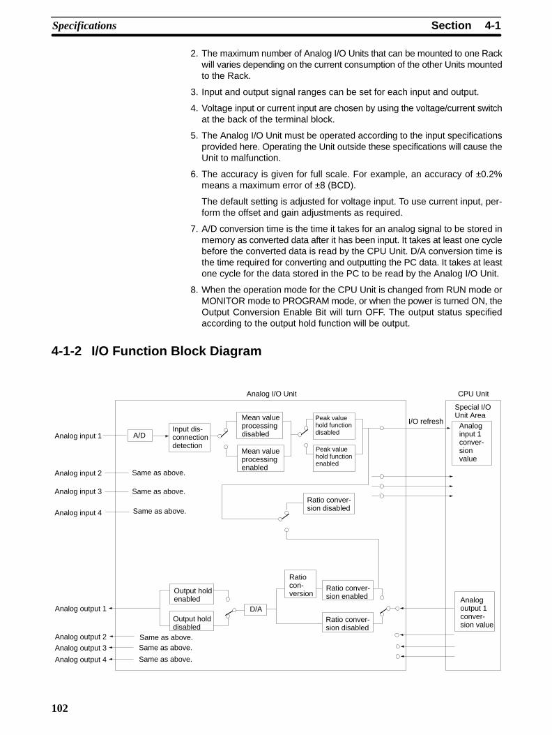
4-1SectionSpecifications
102
2. The maximum number of Analog I/O Units that can be mounted to one Rackwill varies depending on the current consumption of the other Units mountedto the Rack.
3. Input and output signal ranges can be set for each input and output.
4. Voltage input or current input are chosen by using the voltage/current switchat the back of the terminal block.
5. The Analog I/O Unit must be operated according to the input specificationsprovided here. Operating the Unit outside these specifications will cause theUnit to malfunction.
6. The accuracy is given for full scale. For example, an accuracy of ±0.2%means a maximum error of ±8 (BCD).
The default setting is adjusted for voltage input. To use current input, per-form the offset and gain adjustments as required.
7. A/D conversion time is the time it takes for an analog signal to be stored inmemory as converted data after it has been input. It takes at least one cyclebefore the converted data is read by the CPU Unit. D/A conversion time isthe time required for converting and outputting the PC data. It takes at leastone cycle for the data stored in the PC to be read by the Analog I/O Unit.
8. When the operation mode for the CPU Unit is changed from RUN mode orMONITOR mode to PROGRAM mode, or when the power is turned ON, theOutput Conversion Enable Bit will turn OFF. The output status specifiedaccording to the output hold function will be output.
4-1-2 I/O Function Block Diagram
Analog I/O Unit CPU Unit
Special I/OUnit Area
Analoginput 1conver-sionvalue
I/O refresh
Analogoutput 1conver-sion value
Analog input 1
Analog input 2 Same as above.
Input dis-connectiondetection
Mean valueprocessingdisabled
Mean valueprocessingenabled
Peak valuehold functiondisabled
Ratio conver-sion disabled
Ratio conver-sion disabled
Ratio conver-sion enabled
Ratiocon-versionOutput hold
enabled
Output holddisabled
A/D
D/AAnalog output 1
Analog input 3
Analog input 4
Same as above.Analog output 2
Peak valuehold functionenabled
Same as above.
Same as above.
Same as above.Analog output 3
Same as above.Analog output 4

4-1SectionSpecifications
103
4-1-3 Input SpecificationsIf signals that are outside the specified range provided below are input, the con-version values used will be either the maximum or minimum value.
Range: 1 to 5 V (4 to 20 mA)
1 V (4 mA)0.8 V (3.2 mA)
5 V (20 mA)5.2 V (20.8 mA)
Resolution: 4,000
Conversion value (16-bit binary data)
10680FA0
0000FF38
Analog input signal
Range: 0 to 10 V
0 V 10 V–0.5 V 10.5 V
10680FA0
0000FF38
Resolution: 4,000
Conversion value (16-bit binary data)
Analog input signal

4-1SectionSpecifications
104
Range: 0 to 5 V
0 V 5V–0.25 V 5.25 V
10680FA0
0000FF38
Resolution: 4,000
Conversion value (16-bit binary data)
Analog input signal
Range: –10 to 10 V
0 V 10 V11 V
089807D0
F830F768
0000
–10 V–11 V
Resolution: 4,000
Conversion value (16-bit binary data)
Analog input signal
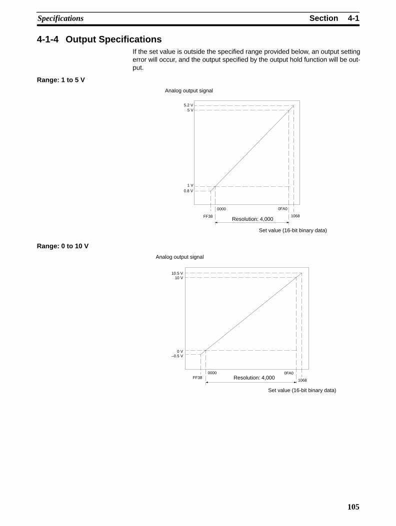
4-1SectionSpecifications
105
4-1-4 Output SpecificationsIf the set value is outside the specified range provided below, an output settingerror will occur, and the output specified by the output hold function will be out-put.
Range: 1 to 5 V
5.2 V5 V
1 V0.8 V
0000
FF38
0FA0
1068Resolution: 4,000
Set value (16-bit binary data)
Analog output signal
Range: 0 to 10 V
0000FF38
0FA0
1068
10.5 V10 V
0 V–0.5 V
Resolution: 4,000
Set value (16-bit binary data)
Analog output signal
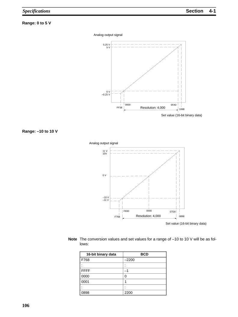
4-1SectionSpecifications
106
Range: 0 to 5 V
0000FF38
0FA0
1068
5.25 V5 V
0 V–0.25 V
Resolution: 4,000
Set value (16-bit binary data)
Analog output signal
Range: –10 to 10 V
0000F830
F768
07D0
0898
0 V
–10 V–11 V
11 V10V
Resolution: 4,000
Set value (16-bit binary data)
Analog output signal
Note The conversion values and set values for a range of –10 to 10 V will be as fol-lows:
16-bit binary data BCD
F768 –2200
: :
FFFF –1
0000 0
0001 1
: :
0898 2200

4-2SectionOperating Procedure
107
4-2 Operating Procedure
Follow the procedure outlined below when using Analog I/O Units.
Installation and Settings
1, 2, 3... 1. Set the DIP switch on the rear panel of the Unit to normal mode.
2. Set the voltage/current switch at the back of the terminal block.
3. Wire the Unit.
4. Use the unit number switch on the front panel of the Unit to set the unit num-ber.
5. Turn ON the power to the PC.
6. Create the I/O tables.
7. Make the Special I/O Unit DM Area settings.
• Set the I/O numbers to be used.
• Set the input and output signal ranges.
• Set the number of mean processing samplings.
• Set the output hold function.
• Set the ratio conversion usage, the ratio set value, and the bias value.
8. Power up the PC again or turn the Special I/O Unit Restart Bit to ON and thenOFF again.
When the input or output of the connected devices needs to be calibrated, followthe procedures in Offset Gain Adjustment below. Otherwise, skip to Operationbelow.
Offset and Gain Adjustment
1, 2, 3... 1. Set the DIP switch on the rear panel of the Unit to adjustment mode.
2. Set the voltage/current switch at the back of the terminal block.
3. Turn ON the power to the PC.
4. Adjust the offset and gain.
5. Turn OFF the power to the PC.
6. Change the setting of the DIP switch on the rear panel of the Unit back tonormal mode.
Operation
1, 2, 3... 1. Turn ON the power to the PC.
2. Ladder program
• Read conversion values or write set values by means of MOV(021) andXFER(070).
• Start and stop conversion output.
• Specify the peak hold function.
• Obtain disconnection notifications and error codes.

4-2SectionOperating Procedure
108
4-2-1 Procedure Examples
CS1W-MAD44 CS1 CPU Unit
Unit No.: 1
Analog input
Analog output
D00100
D00101
D00102
D00103
D00200
D00201
D00202
D00203
IN1: 1 to 5 V
IN2: 0 to 10 V
IN3: 4 to 20 mA
IN4: 4 to 20 mA
OUT1: 1 to 5 V
OUT2: 1 to 5 V
OUT3: –10 to 10 V
OUT4: Not used
Ladd
er P
rogr
am
Setting the Analog I/O Unit
1, 2, 3... 1. Set the operation mode switch on the rear panel of the Unit. Refer to 4-3-4Operation Mode Switch for further details.
Turn OFF SW1 for normal mode
2. Set the voltage/current switch. Refer to 4-3-4 Voltage/Current Switch for fur-ther details.
Pins IN1 to IN4 correspond to analog inputs 1 to 4.
E.g., To use voltage input for analog inputs 1 and 2,turn OFF IN1 and IN2.
To use current input for analog inputs 3 and 4, turnON IN3 and IN4.

4-2SectionOperating Procedure
109
3. Mount and wire the Analog I/O Unit. Refer to 1-2-1 Mounting Procedure, 4-4Wiring or 4-4-4 I/O Wiring Example for further details.
4. Set the unit number switch. Refer to 4-3-2 Unit Number Switch for furtherdetails.
If the unit number is set to 1,words will be allocated to theSpecial I/O Unit Area CIO 2010to CIO 2019 and to the SpecialI/O Unit Area D20100 to D20199.
5. Turn ON the power to the PC.
Power ON

4-2SectionOperating Procedure
110
Creating I/O TablesAfter turning ON the power to the PC, be sure to create the I/O tables.
Peripheral port
Initial Data Settings
1, 2, 3... 1. Specify the Special I/O Unit DM Area settings. Refer to DM Allocation andContents on page 123 for further details.
Peripheral port
Setting conditions
Unit No. 1
Analog input 1: 1 to 5 VAnalog input 2: 0 to 10 VAnalog input 3: 4 to 20 mAAnalog input 4: 4 to 20 mA
Analog output 1: 1 to 5 VAnalog output 2: 1 to 5 VAnalog output 3: –10 to 10 VAnalog output 4: Not used.
• The following diagram shows the input and output settings used. Refer to4-6-1 Input Settings and Conversion Values or 4-7-1 Output Settings andConversions for more details.
15 14 13 12 11 10 09 08 07 06 05 01 0004 03 02
0 0 0 0 0 0 0 0 1 1 1 1 0 1 1 1
Bit
All used
Input 4
Input 3
Input 2
Input 1
Not used Output 4
Output 3
Output 2
Output 1Used
m: DM20100(00F7 Hex)

4-2SectionOperating Procedure
111
• The following diagram shows the input and output range settings. Refer to4-6-1 Input Settings and Conversion Values or 4-7-1 Output Settings andConversions for more details.
15 14 13 12 11 10 09 08 07 06 05 01 0004 03 02
1 0 1 0 0 1 1 0 0 0 0 0 1 0 1 0
Bit
m+1: DM20101(A60A Hex)
Output 1: 1 to 5 V. Set to 10.
Output 2: 1 to 5 V. Set to 10.
Output 3: –10 to 10 V. Set to 00.
Output 4: Not used. Set to 00 (disabled).
Input 1: 1 to 5 V. Set to 10.
Input 2: 0 to 10 V. Set to 01.
Input 3: 4 to 20 mA. Set to 10.
Input 4: 4 to 20 mA. Set to 10.
2. Restart the CPU Unit.
Power turned ON again (or Special I/O Unit Restart Bit is turned ON)
Creating Ladder ProgramsPeripheral port
1, 2, 3... 1. The following example describes how to use analog inputs.
The data that is converted from analog to digital and output to CIO words (n + 5)to (n + 8) of the Special I/O Unit Area (CIO 2015 to CIO 2018), is stored in thespecified addresses D00100 to D00103 as signed binary values 0000 to 0FA0Hex.

4-2SectionOperating Procedure
112
• The following table shows the addresses used for analog input.
Input number Input signalrange
Input conversionvalue address
(n = CIO 2010)
(See note 1.)
Conversion dataholding address
(See note 2.)
1 1 to 5 V (n+5) = CIO 2015 D00100
2 0 to 10 V (n+6) = CIO 2016 D00101
3 4 to 20 mA (n+7) = CIO 2017 D00102
4 4 to 20 mA (n+8) = CIO 2018 D00103
Note a) The addresses are set according to the unit number of the SpecialI/O Unit. Refer to 4-3-2 Unit Number Switch for further details.
b) Set as required.
201904 Input 1 Disconnection Detection Flag (See note c.)
201905 Input 2 Disconnection Detection Flag (See note c.)
201906 Input 3 Disconnection Detection Flag (See note c.)
201907 Input 4 Disconnection Detection Flag (See note c.)
For 1 to 5 V, the hexadecimal value 0000to 0FA0 will be stored in CIO 2015, so ifthere is no disconnection (i.e., 201904 isOFF), CIO 2015 will be stored inD00100.
In the same way, for 0 to 10 V, CIO 2016will be stored in D00101.
In the same way, for 4 to 20 mA, CIO 2017will be stored in D00102.
In the same way, for 4 to 20 mA, CIO 2018will be stored in D00103.
MOV (021)
2015
D00100
MOV (021)
2016
D00101
MOV (021)
2017
D00102
MOV (021)
2018
D00103
c) The input Disconnection Detection Flag is allocated to bits 04 to07 of word (n + 9). Refer to Allocations for Normal Mode on page127 and 4-6-4 Input Disconnection Detection Function for furtherdetails.
2. The following example shows how to use analog outputs.
The setting address D00200 is stored in words (n + 1) to (n + 3) of the Special I/OUnit Area (CIO 2011 to CIO 2013) as a signed binary value between 0000 to0FA0 Hex.
• The following table shows the addresses used for analog output.
Output number Input signalrange
Output settingaddress
(n = CIO 2010)
See note 1.
Originalconversion
address
1 1 to 5 V (n+1) = CIO 2011 D00200
2 0 to 10 V (n+2) = CIO 2012 D00201
3 –10 to 10 V (n+3) = CIO 2013 D00202
4 Not used. --- ---
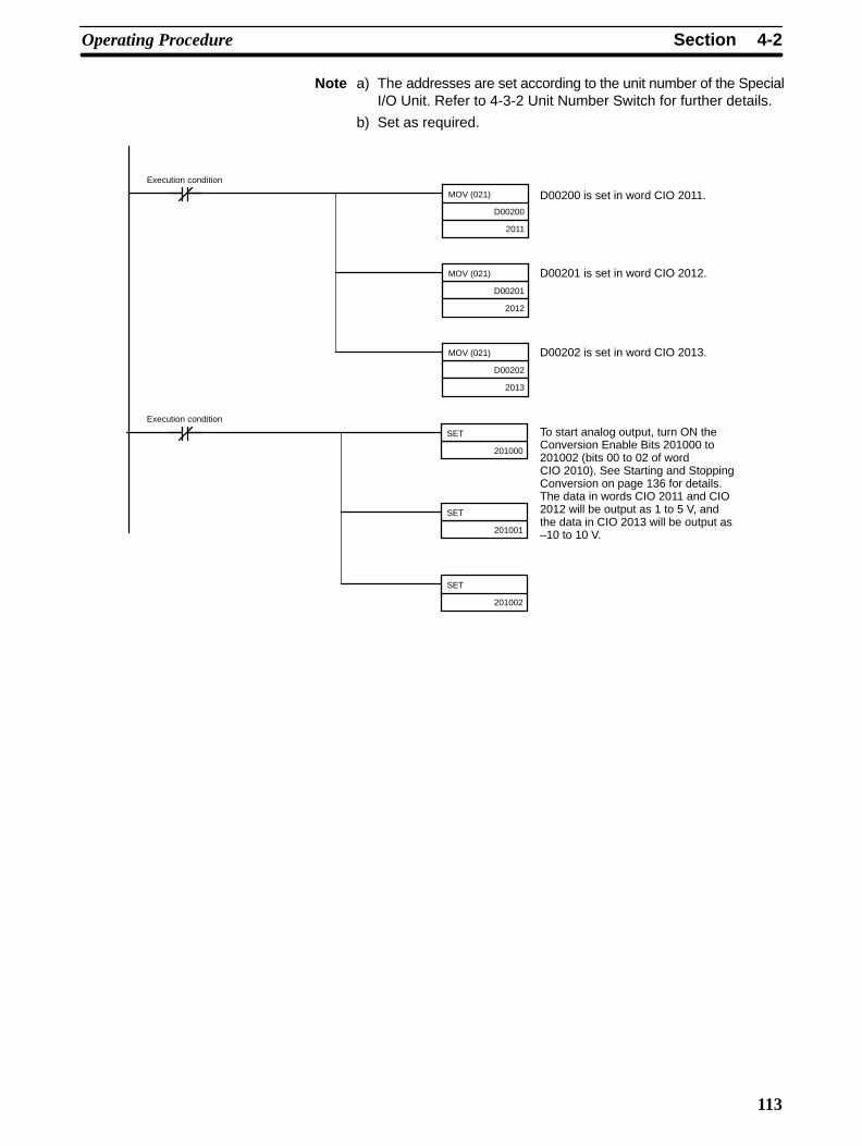
4-2SectionOperating Procedure
113
Note a) The addresses are set according to the unit number of the SpecialI/O Unit. Refer to 4-3-2 Unit Number Switch for further details.
b) Set as required.
D00200 is set in word CIO 2011.
D00201 is set in word CIO 2012.
D00202 is set in word CIO 2013.
To start analog output, turn ON theConversion Enable Bits 201000 to201002 (bits 00 to 02 of wordCIO 2010). See Starting and StoppingConversion on page 136 for details.The data in words CIO 2011 and CIO2012 will be output as 1 to 5 V, andthe data in CIO 2013 will be output as–10 to 10 V.
MOV (021)
D00200
2011
MOV (021)
D00201
2012
Execution condition
MOV (021)
D00202
2013
SET
201000
SET
201002
SET
201001
Execution condition

4-3SectionComponents and Switch Settings
114
4-3 Components and Switch Settings
Unit numbersetting switch
External terminalblock (M3)
External ter-minal blockmountingscrews(black M3)
FrontMounting to terminal block Removing from terminal block
Voltage/Currentswitch
Operation mode switch
Backplane connector
Terminal block
SideBack

4-3SectionComponents and Switch Settings
115
The terminal block is attached by a connector. It can be removed by looseningthe two black mounting screws located at the top and bottom of the terminalblock.
Check to be sure that the black terminal block mounting screw is securely tight-ened to a torque of 0.5 N m.
Fasten the mounting screw.
Fasten the mounting screw.
4-3-1 Indicators
The indicators show the operating status of the Unit. The following table showsthe meanings of the indicators.
LED Meaning Indicator Operating statusRUN Operating Lit Operating in normal mode.(green) Not lit Unit has stopped exchanging data with
the CPU Unit.ERC (red) Error
detected byUnit
Lit Alarm has occurred (such asdisconnection detection) or initialsettings are incorrect.
Not lit Operating normally.
ADJ(yellow)
Adjusting Flashing Operating in offset/gain adjustmentmode.
Not lit Other than the above.
ERH (red) Error in theCPU Unit
Lit Error has occurred during dataexchange with the CPU Unit.
Not lit Operating normally.
4-3-2 Unit Number Switch
The CPU Unit and Analog I/O Unit exchange data via the Special I/O Unit Areaand the Special I/O Unit DM Area. The Special I/O Unit Area and Special I/O UnitDM Area word addresses that each Analog I/O Unit occupies are set by the unitnumber switch on the front panel of the Unit.

!
!
4-3SectionComponents and Switch Settings
116
Always turn OFF the power before setting the unit number. Use a flat-bladescrewdriver, being careful not to damage the slot in the screw. Be sure not toleave the switch midway between settings.
Switchsetting
Unitnumber
Special/O Unit Areaaddresses
Special I/O Unit DM Areaaddresses
0 Unit #0 CIO 2000 to CIO 2009 D20000 to D20099
1 Unit #1 CIO 2010 to CIO 2019 D20100 to D20199
2 Unit #2 CIO 2020 to CIO 2029 D20200 to D20299
3 Unit #3 CIO 2030 to CIO 2039 D20300 to D20399
4 Unit #4 CIO 2040 to CIO 2049 D20400 to D20499
5 Unit #5 CIO 2050 to CIO 2059 D20500 to D20599
6 Unit #6 CIO 2060 to CIO 2069 D20600 to D20699
7 Unit #7 CIO 2070 to CIO 2079 D20700 to D20799
8 Unit #8 CIO 2080 to CIO 2089 D20800 to D20899
9 Unit #9 CIO 2090 to CIO 2099 D20900 to D20999
10 Unit #10 CIO 2100 to CIO 2109 D21000 to D21099
~ ~ ~ ~
n Unit #n CIO 2000 + (n x 10) toCIO 2000 + (n x 10) + 9
D20000 + (n x 100) to D20000 + (n x 100) + 99
~ ~ ~ ~
95 Unit #95 CIO 2950 to CIO 2959 D29500 to D29599
Note If two or more Special I/O Units are assigned the same unit number, an “UNITNo. DPL ERR” error (in the Programming Console) will be generated (A40113will turn ON) and the PC will not operate.
4-3-3 Operation Mode Switch
The operation mode switch on the back panel of the Unit is used to set the opera-tion mode to either normal mode or adjustment mode (for adjusting offset andgain).
Pin number Mode
1 2
OFF OFF Normal mode
ON OFF Adjustment mode
Caution Do not set the pins to any combination other than those shown in the abovetable. Be sure to set pin 2 to OFF.
Caution Be sure to turn OFF the power to the PC before installing or removing the Unit.

!
4-4SectionWiring
117
4-3-4 Voltage/Current SwitchThe analog conversion input can be switched from voltage input to current inputby changing the pin settings on the voltage/current switch located on the back ofthe terminal block.
IN2: Input 2
IN1: Input 1
OFF: Voltage input
ON: Current input
IN4: Input 4
IN3: Input 3
Caution Be sure to turn OFF the power to the PC before mounting or removing the termi-nal block.
4-4 Wiring
4-4-1 Terminal ArrangementThe signal names corresponding to the connecting terminals are as shown in thefollowing diagram.
Output 2 (+) B1
Output 2 (–) B2
Output 4 (+) B3
Output 4 (–) B4
NC B5
Input 2 (+) B6
Input 2 (–) B7
AG B8
Input 4 (+) B9
Input 4 (–) B10
A1
A2
A3
A4
A5
A6
A7
A8
A9
A10
A11
Output 1 (+)
Output 1 (–)
Output 3 (+)
Output 3 (–)
NC
Input 1 (+)
Input 1 (–)
AG
Input 3 (+)
Input 3 (–)
NC
Note 1. The analog I/O numbers that can be used are set in the Data Memory (DM).
2. The I/O signal ranges for individual inputs and outputs are set in the DataMemory (DM). They can be set in units of I/O numbers.
3. The AG terminal (A8, B8) is connected to the 0-V analog circuit in the Unit.Connecting shielded input lines can improve noise resistance.
4. The NC terminals (A5, A11, B5) are not connected to internal circuitry.

4-4SectionWiring
118
4-4-2 Internal Circuitry
The following diagrams show the internal circuitry of the analog I/O section.
Input Circuitry
1 MΩ
15 kΩ 15 kΩ
15 kΩ 15 kΩ
AG (common to all inputs)
Input (+)
Input (–)
AG(analog0 V)
Input circuitandconversioncircuit
1 MΩ
Voltage/currentinput switch
250 Ω
Output Circuitry
Outputswitch andconversioncircuit
AMP Voltageoutput (+)
Voltageoutput (–)
AG (common to all outputs)
Internal Configuration
Bus interface
Indicators/Switch
MPU Multi-plexerandamplifier
Multi-plexerandamplifier
OUTPUT
RegulatorInsulation-typeDC-to-DC converter
D/A converter
A/D converter INPUT
Externallyconnectedterminal
Oscillator
Division
CS1 Series
EEPROM
Pho
toco
uple
r in
sula
tion
RAM ROM

4-4SectionWiring
119
4-4-3 Voltage Input Disconnection
Connected device #1
24 VDC
Connecteddevice #2
Note If the connected device #2 in the above example outputs 5 V and the power sup-ply is shared by 2 channels as shown in the above diagram, approximately onethird of the voltage, or 1.6 V, will be input at input 1.
When voltage inputs are used and a disconnection occurs, separate the powersupply at the side of the connected devices or use an insulating device (isolator)for each input to avoid the following problems.
When the power supply at the connected devices is shared and section A or B isdisconnected, power will flow in the direction of the broken line and the outputvoltage of the other connected devices will be reduced to between a third to ahalf of the voltage. If 1 to 5 V is used and the reduced voltage output, disconnec-tion may not be detectable. If section C is disconnected, the power at the (–)input terminal will be shared and disconnection will not be detectable.
For current inputs, sharing the power supply between the connected devices willnot cause any problems.

4-4SectionWiring
120
4-4-4 I/O Wiring Example
A7
A10
B1
B2
B3
B4
B5
B6
B7
B8
B9
B10
A1
A2
A3
A4
A5
A6
A8
A9
A11
Output 2(Voltage output)
Input 2(Voltage input)
CS1W-MAD44
Shield
Shield
See note 4See note 4
Shield
Input 1(Current input)
+
–
+
–
Note 1. When using current inputs, pins IN1 to IN4 of the voltage/current switchmust be set to ON. Refer to 4-3-4 Voltage/Current Switch for further details.
2. For inputs that are not used, either set to “0: Not used” in the input numbersettings (refer to 4-6-1 Setting Inputs and Signal Ranges) or short-circuit thevoltage input terminals (V+) and (V–).
3. Crimp-type terminals must be used for terminal connections, and thescrews must be tightened securely. Use M3 screws and tighten them to atorque of 0.5 N m.
4. When connecting the shield of the analog input cables to the Unit’s AG ter-minals (A8, B8), as shown in the previous diagram, use a wire that is 30 cmmax. in length if possible.
6.0 mm max.
6.0 mm max.M3 screw
Fork type
Round type
Connecting shielded cable to the Unit’s AG terminals (A8, B8) can improve noiseresistance.
To minimize output wiring noise, ground the output signal line to the input device.
4-4-5 I/O Wiring ConsiderationsWhen wiring inputs, apply the following points to avoid noise interference andoptimize Analog I/O Unit performance.
• Use two-core shielded twisted-pair cables for external connections.
• Route I/O cables separately from the AC cable, and do not run the Unit’scables near a main circuit cable or a high voltage cable. Do not insert outputcables into the same duct.
• If there is noise interference from power lines (if, for example, the power supplyis shared with electrical welding devices or electrical discharge machines, or ifthere is a high-frequency generation source nearby) install a noise filter at thepower supply input area.

4-5SectionExchanging Data with the CPU Unit
121
4-5 Exchanging Data with the CPU Unit
4-5-1 Outline of Data ExchangeData is exchanged between the CPU Unit and the CS1W-MAD44 Analog I/OUnit via the Special I/O Unit Area (for data used to operate the Unit) and the Spe-cial I/O Unit DM Area (for data used for initial settings).
I/O Refresh DataAnalog input conversion values 1 to 4, analog output setting values 1 to 4, andother data used to operate the Unit are allocated in the Special I/O Unit Area ofthe CPU Unit according to the unit number, and are exchanged during I/Orefreshing.
Fixed DataThe Unit’s fixed data, such as the analog input signal ranges 1 to 4 and analogoutput signal ranges 1 to 4, is allocated in the Special I/O Unit DM Area of theCPU Unit according to the unit number, and is exchanged when the power isturned ON or the Unit is restarted.
CS1 CPU Unit CS1W-MAD44 Analog I/O Unit
Special I/O Unit Area I/O Refresh Data
Analog inputs
Analog outputs
DM (Data Memory) Area
Input signal range
Output signal range
I/O refresh
Power ON orUnit restart
Exchanges normal datasuch as analog inputs 1 to4 and analog outputs 1 to4.
See 4-5-5 I/ORefresh DataAllocations fordetails.
Transmits initial settingssuch as analog inputranges 1 to 4 and analogoutput ranges 1 to 4.
See 4-5-4 FixedData Allocationsfor details.
2000 + n x 10
2000 + n x 10 + 9
D20000 + n x 100
D20000 + n x 100 + 99
10words
100words
Fixed Data
:
:

4-5SectionExchanging Data with the CPU Unit
122
4-5-2 Unit Number Settings
The Special I/O Unit Area and Special I/O Unit DM Area word addresses thateach Analog I/O Unit occupies are set by the unit number switch on the frontpanel of the Unit.
Switchsetting
Unitnumber
Special/O Unit Areaaddresses
Special I/O Unit DM Areaaddresses
0 Unit #0 CIO 2000 to CIO 2009 D20000 to D20099
1 Unit #1 CIO 2010 to CIO 2019 D20100 to D20199
2 Unit #2 CIO 2020 to CIO 2029 D20200 to D20299
3 Unit #3 CIO 2030 to CIO 2039 D20300 to D20399
4 Unit #4 CIO 2040 to CIO 2049 D20400 to D20499
5 Unit #5 CIO 2050 to CIO 2059 D20500 to D20599
6 Unit #6 CIO 2060 to CIO 2069 D20600 to D20699
7 Unit #7 CIO 2070 to CIO 2079 D20700 to D20799
8 Unit #8 CIO 2080 to CIO 2089 D20800 to D20899
9 Unit #9 CIO 2090 to CIO 2099 D20900 to D20999
10 Unit #10 CIO 2100 to CIO 2109 D21000 to D21099
~ ~ ~ ~
n Unit #n CIO 2000 + (n x 10) toCIO 2000 + (n x 10) + 9
D20000 + (n x 100) to D20000 + (n x 100) + 99
~ ~ ~ ~
95 Unit #95 CIO 2950 to CIO 2959 D29500 to D29599
Note If two or more Special I/O Units are assigned the same unit number, an “UNITNo. DPL ERR” error (in the Programming Console) will be generated (A40113will turn ON) and the PC will not operate.
4-5-3 Special I/O Unit Restart Bits
To restart the Unit operations after changing the contents of the data memory orcorrecting an error, turn ON the power to the PC again or turn the Special I/O UnitRestart Bit ON and then OFF again.
Special I/OUnit Area word
address
Function
A50200 Unit No. 0 Restart Bit Restarts the Unit when turned
A50201 Unit No. 1 Restart Bit ON and then OFF again.
~ ~
A50215 Unit No. 15 Restart Bit
A50300 Unit No. 16 Restart Bit
~ ~
A50715 Unit No. 95 Restart Bit
Note If the error is not corrected by restarting the Unit or turning the Special I/O UnitRestart Bit ON and then OFF again, replace the Analog I/O Unit.
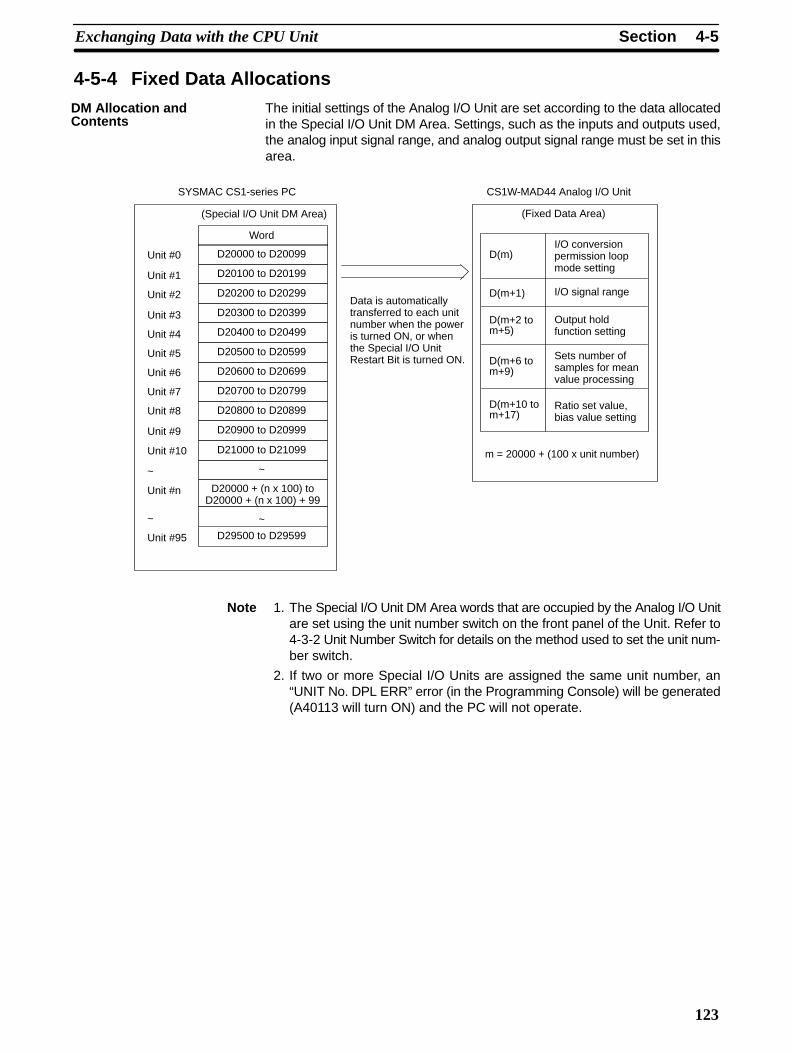
4-5SectionExchanging Data with the CPU Unit
123
4-5-4 Fixed Data AllocationsThe initial settings of the Analog I/O Unit are set according to the data allocatedin the Special I/O Unit DM Area. Settings, such as the inputs and outputs used,the analog input signal range, and analog output signal range must be set in thisarea.
D(m+1)
D(m)
D20300 to D20399
D20400 to D20499
D20500 to D20599
D20000 to D20099
D20100 to D20199
D20200 to D20299
D20900 to D20999
D20600 to D20699
D20700 to D20799
D20800 to D20899
SYSMAC CS1-series PC CS1W-MAD44 Analog I/O Unit
(Fixed Data Area)
Unit #0
Unit #1
Unit #2
Unit #3
Unit #4
Unit #5
Unit #6
Unit #7
Unit #8
Unit #9
(Special I/O Unit DM Area)
Word
D29500 to D29599
D21000 to D21099
~
D20000 + (n x 100) toD20000 + (n x 100) + 99
Unit #10
~
Unit #n
~
Unit #95
D(m+2 tom+5)
D(m+6 tom+9)
D(m+10 tom+17)
I/O conversionpermission loopmode setting
I/O signal range
Output holdfunction setting
Sets number ofsamples for meanvalue processing
Ratio set value,bias value setting
Data is automaticallytransferred to each unitnumber when the poweris turned ON, or whenthe Special I/O UnitRestart Bit is turned ON.
m = 20000 + (100 x unit number)
~
Note 1. The Special I/O Unit DM Area words that are occupied by the Analog I/O Unitare set using the unit number switch on the front panel of the Unit. Refer to4-3-2 Unit Number Switch for details on the method used to set the unit num-ber switch.
2. If two or more Special I/O Units are assigned the same unit number, an“UNIT No. DPL ERR” error (in the Programming Console) will be generated(A40113 will turn ON) and the PC will not operate.
DM Allocation andContents

4-5SectionExchanging Data with the CPU Unit
124
The following table shows the allocation of DM words and bits for both normaland adjustment mode.
DM word Bits
15 14 13 12 11 10 9 8 7 6 5 4 3 2 1 0D(m) Ratio conversion use setting Input use setting Output use setting
Loop 4 Loop 3 Loop 2 Loop 1 Input4
Input3
Input2
Input1
Out-put 4
Out-put 3
Out-put 2
Out-put 1
D(m+1) Input signal range setting Output signal range setting
Input 4 Input 3 Input 2 Input 1 Output 4 Output 3 Output 2 Output 1
D(m+2) Not used. Output 1: Output status when conversion stopped
D(m+3) Not used. Output 2: Output status when conversion stopped
D(m+4) Not used. Output 3: Output status when conversion stopped
D(m+5) Not used. Output 4: Output status when conversion stopped
D(m+6) Input 1: Mean value processing setting
D(m+7) Input 2: Mean value processing setting
D(m+8) Input 3: Mean value processing setting
D(m+9) Input 4: Mean value processing setting
D(m+10) Loop 1 (input 1 to output 1), A constant
D(m+11) Loop 1 (input 1 to output 1), B constant
D(m+12) Loop 2 (input 2 to output 2), A constant
D(m+13) Loop 2 (input 2 to output 2), B constant
D(m+14) Loop 3 (input 3 to output 3), A constant
D(m+15) Loop 3 (input 3 to output 3), B constant
D(m+16) Loop 4 (input 4 to output 4), A constant
D(m+17) Loop 4 (input 4 to output 4), B constant
Note For the DM word addresses, m = 20000 + (100 x unit number).
DM Allocation Contents

4-5SectionExchanging Data with the CPU Unit
125
Set Values and Stored ValuesItem Contents Page
Input Use setting 0: Not used.1: Used.
129
Input signal range 00: –10 to 10 V01: 0 to 10 V10: 1 to 5 V/4 to 20 mA (See note 1.)11: 0 to 5 V
129
Mean value processingsetting
0000: Mean value processing for 2 buffers (See note 3.)0001: No mean value processing0002: Mean value processing for 4 buffers0003: Mean value processing for 8 buffers0004: Mean value processing for 16 buffers0005: Mean value processing for 32 buffers0006: Mean value processing for 64 buffers
130
Output Use setting 0: Not used.1: Used.
135
Output signal range 00: –10 to 10 V01: 0 to 10 V10: 1 to 5 V11: 0 to 5 V
135
Output status when stopped 00: CLR Outputs 0 or minimum value of each range. (See note 2.)
01: HOLD Holds output just before stopping.02: MAX Outputs maximum value of range.
137
Loop Ratio conversion use setting 00: Not used.01: Uses positive gradient conversion.10: Uses negative gradient conversion.11: Same as for setting “00” above.
138
A constant 4 digits BCD (0 to 9999)
B constant 16-bit binary data
Note 1. The input signal range of “1 to 5 V” and “4 to 20 mA” is switched using thepins of the voltage/current switch. Refer to 4-3-4 Voltage/Current Switch fordetails.
2. For the range of ±10 V, the output is 0 V. For other output signal ranges, theminimum value of each signal range is output. Refer to 4-7-2 Output HoldFunction for details.
3. The default of mean value processing setting is set to “Mean value proces-sing for 2 buffers.” Refer to 4-6-2 Mean Value Processing.

4-5SectionExchanging Data with the CPU Unit
126
4-5-5 I/O Refresh Data AllocationsI/O refresh data for the Analog I/O Unit is exchanged according to the allocationsin the Special I/O Unit Area. Analog input converted values 1 to 4 and analogoutput set values 1 to 4 are exchanged with the CPU Unit at I/O refresh.
CIO n + 5to CIO n + 9
CIO n toCIO n + 4
CIO 2030 to CIO 2039
CIO 2040 to CIO 2049
CIO 2050 to CIO 2059
CIO 2000 to CIO 2009
CIO 2010 to CIO 2019
CIO 2020 to CIO 2029
CIO 2090 to CIO 2099
CIO 2060 to CIO 2069
CIO 2070 to CIO 2079
CIO 2080 to CIO 2089
SYSMAC CS1-series PC CS1W-MAD44 Analog I/O Unit
IN refresh
(I/O Refresh Data Area)
Unit #0
Unit #1
Unit #2
Unit #3
Unit #4
Unit #5
Unit #6
Unit #7
Unit #8
Unit #9
(Special I/O Unit Area)
At the I/O refresh by thePC, outputs (CPU toUnit) and inputs (Unit toCPU) are refreshed inorder with every cycle.
OUT refresh
Allocated words
CIO 2950 to CIO 2959
CIO 2100 to CIO 2109
~
CIO 2000 + (n x 10) toCIO 2000 + (n x 10) + 9
Unit #10
~
Unit #n
~
Unit #95
Normal mode
CIO n + 8to CIO n + 9
CIO n toCIO n + 7
IN refresh
OUT refresh
Adjustment mode
n = 2000 + (10 x unit number)
~
I/O refresh
Note 1. The Special I/O Unit Area words that are occupied by the Analog I/O Unit areset using the unit number switch on the front panel of the Unit. Refer to 4-3-2Unit Number Switch for details on the method used to set the unit numberswitch.
2. If two or more Special I/O Units are assigned the same unit number, an“UNIT No. DPL ERR” error (in the Programming Console) will be generated(A40113 will turn ON) and the PC will not operate.
Special I/O Unit AreaAllocation and Contents

4-5SectionExchanging Data with the CPU Unit
127
For normal mode, set the operation mode switch on the rear panel of the Unit asshown in the following diagram.
The allocation of words and bits in the CIO Area is shown in the following table.
I/O Word Bits
15 14 13 12 11 10 9 8 7 6 5 4 3 2 1 0Output n Not used. Peak value hold Conversion enable(CPU toUnit)
Input
4
Input
3
Input
2
Input
1
Out-
put 4
Out-
put 3
Out-
put 2
Out-
put 1
n + 1 Output 1 set value
163 162 161 160
n + 2 Output 2 set value
n + 3 Output 3 set value
n + 4 Output 4 set value
Input n + 5 Input 1 conversion value / Loop 1 calculation result(Unit to 163 162 161 160CPU)
n + 6 Input 2 conversion value / Loop 2 calculation result
n + 7 Input 3 conversion value / Loop 3 calculation result
n + 8 Input 4 conversion value / Loop 4 calculation result
n + 9 Alarm Flags Disconnection detec-tion
Output setting error
Input
4
Input
3
Input
2
Input
1
Out-
put 4
Out-
put 3
Out-
put 2
Out-
put 1
Set Values and Stored ValuesI/O Item Contents Page
Input Peak value hold function 0: Not used.1: Peak value hold used.
133
Conversion value
Calculation result
16-bit binary data 130
Disconnection detection 0: No disconnection1: Disconnection
134
Output Conversion enable 0: Conversion output stopped.1: Conversion output begun.
136
Set value 16-bit binary data 135
Output setting error 0: No error1: Output setting error
138
Common Alarm Flags Bits 00 to 03: Output set value errorBits 04 to 07: Input disconnection detectionBit 08: Ratio conversion use setting errorBit 09: Ratio set value errorBit 10: Output hold setting error Bit 11: Mean value processing setting errorBit 15: Operating in adjustment mode
(always 0 in normal mode)
157
158
Note For the CIO word addresses, n = 2000 + 10 x unit number.
The input disconnection detection function can be used when the input signalrange is set for 1 to 5 V (4 to 20 mA).
Input signal range Voltage/current
1 to 5 V 0.3 V max.
4 to 20 mA 1.2 mA max.
Allocations for NormalMode

4-5SectionExchanging Data with the CPU Unit
128
For adjustment mode, set the operation mode switch on the rear panel of theUnit as shown in the following diagram. When the Unit is set for adjustmentmode, the ADJ indicator on the front panel of the Unit will flash.
The allocation of CIO words and bits is shown in the following table.
I/O Word Bits
15 14 13 12 11 10 9 8 7 6 5 4 3 2 1 0Output n Not used. Inputs and outputs to be adjusted(CPU to 161 160Unit)
n + 1 Not used. Not used. Clr Set Up Down Gain Off-set
n + 2 Not used.
n + 3 Not used.
n + 4 Not used.
n + 5 Not used.
n + 6 Not used.
n + 7 Not used.
Input n + 8 Conversion value or set value at time of adjustment(Unit toCPU) 163 162 161 160
n + 9 Alarm Flags Disconnection detec-tion
Not used.
Input
4
Input
3
Input
2
Input
1
Refer to 4-9-1 Adjustment Mode Operational Flow for further details.
Item Contents
Input or output to beadjusted
Sets input or output to be adjusted.Leftmost digit: 1 (output) or 2 (input)Rightmost digit: 1 to 4
Offset (Offset Bit) When ON, adjusts offset error.
Gain (Gain Bit) When ON, adjusts gain error.
Down (Down Bit) Decrements the adjustment value while ON.
Up (Up Bit) Increments the adjustment value while ON.
Set (Set Bit) Sets adjusted value and writes to EEPROM.
Clr (Clear Bit) Clears adjusted value. (Returns to default status)
Conversion value foradjustment
The conversion value for adjustment is stored as 16bits of binary data.
Disconnection detection 0: No disconnection1: Disconnection
Alarm Flags Bit 12: Input value is outside adjustment limits (inadjustment mode)Bit 13: I/O number setting error (in adjustment mode)Bit 14: EEPROM write error (in adjustment mode)Bit 15: Operating in adjustment mode
(always 1 in adjustment mode)
Note For the CIO word addresses, n = 2000 + (10 x unit number).
Allocation forAdjustment Mode
Set Values and StoredValues

4-6SectionAnalog Input Functions and Operating Procedures
129
The input disconnection detection function can be used when the input signalrange is set for 1 to 5 V (4 to 20 mA).
Input signal range Voltage/current
1 to 5 V 0.3 V max.
4 to 20 mA 1.2 mA max.
4-6 Analog Input Functions and Operating Procedures
4-6-1 Input Settings and Conversion Values
Setting Inputs and Signal RangesThe Analog I/O Unit converts only analog inputs specified by input numbers 1 to4. To specify the analog inputs to be used, turn ON from a Programming Devicethe D(m) bits in the DM Area shown in the following diagram.
15 14 13 12 11 10 09 08 07 06 05 04 03 02 01 00Bit
D(m)
Inpu
t 2
Inpu
t 1
0: Not used
1: Used
Inpu
t 4
Inpu
t 3
The analog input sampling interval can be shortened by setting any unused inputnumbers to 0.
Sampling interval = (1 ms) x (Number of inputs used)
For the DM word addresses, m = 20000 + (100 x unit number)
The word for inputs that have been set to “Not used” will always be “0000.”
Any of four types of input signal range (–10 to 10 V, 0 to 10 V, 1 to 5 V, and 4 to20 mA) can be selected for each of the inputs (i.e., input numbers 1 to 4). Tospecify the input signal range for each input, set from a Programming Device theD(m + 1) bits in the DM Area as shown in the following diagram.
15 14 13 12 11 10 09 08 07 06 05 04 03 02 01 00Bit
DM (m+1)
Inpu
t 2
Inpu
t 1
00: -10 to 10 V01: 0 to 10 V10: 1 to 5 V / 4 to 20 mA11: 0 to 5 V
Inpu
t 4
Inpu
t 3
Note 1. For the DM word addresses, m = 20000 + (100 x unit number)
2. The input signal range of “1 to 5 V” or “4 to 20 mA” is switched using the volt-age/current switch.
3. After making the DM settings from a Programming Device, it will be neces-sary to either power up the PC again or turn ON the Special I/O Unit RestartBit in order to transfer the contents of the DM settings to the Special I/O Unit.
Input Numbers
Input Signal Range

4-6SectionAnalog Input Functions and Operating Procedures
130
Analog input conversion values are stored for each input number, in CIO wordsn+5 to n+8.
Word Function Stored value
n+5 Input 1 conversion value 16-bit binary data
n+6 Input 2 conversion value
n+7 Input 3 conversion value
n+8 Input 4 conversion value
Note For the CIO word addresses, n = 2000 + (10 x unit number).
Use MOV(021) or XFER(070) to read conversion values in the user program.
In this example, the conversion data from only one input is read. (The unit num-ber is 0.)
MOV(021)
2005
D00001
Input conditionConversion data in CIO word2005 (input number 1) is readto D00001.
In this example, the conversion data from multiple inputs is read. (The unit num-ber is 0.)
XFER(070)
#0004
2005
D00001
Input conditionConversion data in CIO words2005 and 2008 (input num-bers 1 and 4) is read toD00001 and D00004.
For details regarding conversion value scaling, refer to Scaling on page 168.
4-6-2 Mean Value ProcessingThe Analog I/O Unit can compute the mean value of the conversion values ofanalog inputs that have been previously sampled. Mean value processinginvolves an operational mean value in the history buffers, so it has no effect onthe data refresh cycle. (The number of history buffers that can be set to usemean value processing is 2, 4, 8, 16, 32, or 64.)
Conversion data Buffer 1
Buffer 2
Buffer 3
Buffer 4
Buffer n
(Mean valueprocessing)
Conversion value
(Values stored inCIO words n+5 andn+8)
(Discarded)
When “n” number of history buffers are being used, the first conversion data willbe stored for all “n” number of history buffers immediately after data conversionhas begun or after a disconnection is restored.
Reading ConversionValues
Example 1
Example 2

4-6SectionAnalog Input Functions and Operating Procedures
131
When mean value processing is used together with the peak value hold function,the mean value will be held.
To specify whether or not mean value processing is to be used, and to specify thenumber of history buffers for mean data processing, use a Programming Deviceto make the settings in D(m+6) to D(m+9) as shown in the following table.
DM word Function Set value
D(m+6) Input 1 mean value processing 0000: Mean value processing with 2 buffers
D(m+7) Input 2 mean value processing0001: No mean value processing0002: Mean value processing with 4 buffers
D(m+8) Input 3 mean value processing0003: Mean value processing with 8 buffers0004: Mean value processing with 16 buffers
D(m+9) Input 4 mean value processing 0005: Mean value processing with 32 buffers0006: Mean value processing with 64 buffers
For the DM word addresses, m = 20000 + (100 x unit number)
Note After making the DM settings from a Programming Device, it will be necessary toeither power up the PC again or turn ON the Special I/O Unit Restart Bit to trans-fer the contents of the DM settings to the Special I/O Unit.
The history buffer operational means are calculated as shown below. (In thisexample, there are four buffers.)
1, 2, 3... 1. With the first cycle, Data 1 is stored in all the history buffers.
(Mean valueprocessing)
Conversion value
Data 1
Data 1
Data 1
Data 1
Mean value = (Data 1 + Data 1 + Data 1 + Data 1) 4
2. With the second cycle, Data 2 is stored in the first history buffer.
(Mean valueprocessing)
Conversion value
Data 2
Data 1
Data 1
Data 1
Mean value = (Data 2 + Data 1 + Data 1 + Data 1) 4
3. With the third cycle, Data 3 is stored in the first history buffer.
(Mean valueprocessing)
Conversion value
Data 3
Data 2
Data 1
Data 1
Mean value = (Data 3 + Data 2 + Data 1 + Data 1) 4

4-6SectionAnalog Input Functions and Operating Procedures
132
4. With the fourth cycle, the Data 4 is stored in the first history buffer.
(Mean valueprocessing)
Conversion value
Data 4
Data 3
Data 2
Data 1
Mean value = (Data 4 + Data 3 + Data 2 + Data 1) 4
5. With the fifth cycle, Data 5 is stored in the first history buffer.
(Mean valueprocessing)
Conversion value
Data 5
Data 4
Data 3
Data 2
Mean value = (Data 5 + Data 4 + Data 3 + Data 2) 4
When a disconnection is restored, the mean value processing function beginsagain from step 1.
Note The default setting for mean value processing in the Analog I/O Unit is meanvalue processing with 2 buffers. The response time for the default setting is dif-ferent from when there is no mean processing, as shown in the following dia-gram.
Input signal to the Unit (V)
Conversion data
Time (ms)
Time (ms)
t: Delay
V = 20 V (–10 to 10 V)(Actual measured value for 1 word)
Mean value processingwith 2 buffers
No mean valueprocessing
t = 6.5 ms t = 10.5 ms
The approximate value of t is as follows:
For 1 word:
t = n + (2 to 3) (ms)n = Number of buffers
For m words, 1 < m 4:
t = (n – 2) m + 10.5 (ms)
E.g., For 8 buffers and 4 words, t = 34.5 ms
Specify “no mean value processing” to follow conversion of a rapid change ininput signals.

4-6SectionAnalog Input Functions and Operating Procedures
133
4-6-3 Peak Value Hold Function
The peak value hold function holds the maximum digital conversion value forevery input (including mean value processing). This function can be used withanalog input. The following diagram shows how digital conversion values areaffected when the peak value hold function is used.
Peak value hold
Digital conversion value
t (Time)
Conversion value whenthe peak value holdfunction is used
The peak value hold function can be set individually for each input number byturning on the respective bits (04 to 07) in CIO word n.
15 14 13 12 11 10 09 08 07 06 05 04 03 02 01 00Bit
Inpu
t 2
Inpu
t 1
Word n
The peak value hold function will be in effectfor the above input numbers while theirrespective bits are ON. The conversionvalues will be reset when the bits are turnedOFF.
Inpu
t 4
Inpu
t 3
For the CIO word addresses, n = 2000 + (10 x unit number).
In the following example, the peak value hold function is in effect for input num-ber 1, and the unit number is 0.
200004
Input conditionThe maximumconversiondata value isheld for inputnumber 1.
When mean value processing is used together with the peak value hold function,the mean value will be held.
As long as the peak value hold function is in effect, the peak value hold will beheld even in the event of a disconnection.
When the load to the CPU Unit is disconnected, the Peak Value Hold Bits (bits 04to 07 of the word n) are cleared and the peak value hold function is disabled.

4-6SectionAnalog Input Functions and Operating Procedures
134
4-6-4 Input Disconnection Detection FunctionWhen an input signal range of 1 to 5 V (4 to 20 mA) is used, input circuit discon-nections can be detected. The detection conditions for each of the input signalranges are shown in the following table.
Range Current/voltage
1 to 5 V 0.3 V max.
4 to 20 mA 1.2 mA max.
The current/voltage level will fluctuate according to the offset/gain adjustment.
The input disconnection detection signals for each input number are stored inbits 04 to 07 of CIO word n+9. Specify these bits as execution conditions to usedisconnection detection in the user’s program.
15 14 13 12 11 10 09 08 07 06 05 04 03 02 01 00Bit
Inpu
t 2
Inpu
t 1
Word n+9
The respective bit turns ON when adisconnection is detected for a giveninput. When the disconnection isrestored, the bit turns OFF.
Inpu
t 4
Inpu
t 3
For the CIO word addresses, n = 2000 + (10 x unit number).
The conversion value during a disconnection will be 0000.
In the following example, the conversion value is read only if there is no discon-nection at analog input number 1. (The unit number is 0.)
MOV (021)
2005
D00001
200904The conver-sion value inCIO word2005 (inputnumber 1) isread toD00001.

4-7SectionAnalog Output Functions and Operating Procedures
135
4-7 Analog Output Functions and Operating Procedures
4-7-1 Output Settings and Conversions
Setting Outputs and Signal RangesThe Analog I/O Unit converts analog outputs specified by output numbers 1 to 4only. To specify the analog outputs to be used, turn ON from a ProgrammingDevice the D(m) bits in the DM Area shown in the following diagram.
15 14 13 12 11 10 09 08 07 06 05 04 03 02 01 00Bit
D(m)
Out
put 2
Out
put 1
0: Not used1: Used
Out
put 4
Out
put 3
The analog output conversion cycle can be shortened by setting any unusedoutput numbers to 0.
Conversion cycle = (1 ms) x (Number of outputs used)
Note 1. For the DM word addresses, m = 20000 + (100 x unit number).
2. Output numbers not used (set to 0) will be output at 0 V.
Any of four types of output signal range (–10 to 10 V, 0 to 10 V, 1 to 5 V, and 0 to5 V) can be selected for each of the outputs (i.e., output numbers 1 to 4). Tospecify the output signal range for each output, use a Programming Device toset the D(m+1) bits in the DM Area shown in the following diagram.
15 14 13 12 11 10 09 08 07 06 05 04 03 02 01 00Bit
D(m + 1)
Out
put 2
Out
put 1
00: -10 to 10 V01: 0 to 10 V10: 1 to 5 V11: 0 to 5 V
Out
put 4
Out
put 3
Note 1. For the DM word addresses, m = 20000 + (100 x unit number).
2. After making the DM settings from a Programming Device, it will be neces-sary to either power up the PC again or turn ON the Special I/O Unit RestartBit to transfer the contents of the DM settings to the Special I/O Unit.
Analog output set values are written to CIO words (n+1) to (n+4).
Word Function Stored value
n+1 Output 1 set value 16-bit binary data
n+2 Output 2 set value
n+3 Output 3 set value
n+4 Output 4 set value
Output Numbers
Output Signal Range
Writing Set Values

4-7SectionAnalog Output Functions and Operating Procedures
136
For the CIO word addresses, n = 2000 + (10 x unit number).
Use MOV(021) or XFER(070) to write values in the user program.
In this example, the set value from only one input is read. (The unit number is 0.)
MOV (021)
D00001
2001
Input condition
The set value stored in D 00001is written to CIO word 2001 (out-put number 1).
In this example, multiple set values are written. (The unit number is #0.)
XFER(070)
#0004
D00001
2001
Input condition
The set values stored in D 00001to D 00004 are written to CIO words2001 to 2004 (outputs 1 to 4).
Note If the set value has been written outside the specified range, an output settingerror will occur, and the value set by the output hold function will be output.
To begin analog output conversion, turn ON the corresponding ConversionEnable Bit (word n, bits 00 to 03) from the user’s program.
15 14 13 12 11 10 09 08 07 06 05 04 03 02 01 00Bit
Out
put 2
Out
put 1
Analog conversion is executed whilethese bits are ON. When the bits areturned OFF, the conversion is stoppedand the output data is held.
Word n
Out
put 4
Out
put 3
For the CIO word addresses, n = 2000 + (10 x unit number).
The analog output when conversion is stopped will differ depending on the out-put signal range setting and output hold setting. Refer to Setting Outputs andSignal Ranges on page 135 and 4-7-2 Output Hold Function.
Conversion will not begin under the following conditions even if the ConversionEnable Bit is turned ON. Refer to 4-7-2 Output Hold Function.
1, 2, 3... 1. In adjustment mode, when something other than the output number is out-put during adjustment.
2. When there is an output setting error.
3. When a fatal error occurs at the PC.
4. When there is an input disconnection during a ratio conversion.
When the operation mode for the CPU Unit is changed from RUN or MONITORmode to PROGRAM mode, or when the power is turned ON, the ConversionEnable Bits will all turn OFF. The output status at this time depends on the outputhold function.
Example 1
Example 2
Starting and StoppingConversion

4-7SectionAnalog Output Functions and Operating Procedures
137
In this example, conversion is begun for analog output number 1. (The unit num-ber is 0.)
200000
Input conditionConversionbegins foroutputnumber 1.
4-7-2 Output Hold FunctionThe Analog I/O Unit stops conversion under the following circumstances andoutputs the value set by the output hold function.
1, 2, 3... 1. When the Conversion Enable Bit is OFF. Refer to Starting and StoppingConversion on page 136.
2. In adjustment mode, when something other than the output number is out-put during adjustment. Refer to 4-9-2 Input Offset and Gain Adjustment Pro-cedures.
3. When there is an output setting error. Refer to 4-7-3 Output Setting Errors.
4. When a fatal error occurs at the PC.
5. When there is an input disconnection during ratio conversion.
6. When there is an I/O bus error.
7. When the CPU Unit is in LOAD OFF status.
8. When there is a WDT (watchdog timer) error in the CPU Unit.
CLR, HOLD, or MAX can be selected for the output status when conversion isstopped.
Output signalrange
CLR HOLD MAX
0 to 10 V –0.5 V (Min.–5%of full scale)
Voltage that was outputjust prior to stop.
10.5 V (Max.+5%of full scale)
–10 to 10 V 0.0 V Voltage that was outputjust prior to stop.
11.0 V (Max.+5%of full scale)
1 to 5 V 0.8 V (Min.–5% offull scale)
Voltage that was outputjust prior to stop.
5.2 V (Max.+5% offull scale)
0 to 5 V –0.25 V (Min.–5%of full scale)
Voltage that was outputjust prior to stop.
5.25 V (Max.+5%of full scale)
The above values may fluctuate if offset/gain adjustment has been applied.
To specify the output hold function, use a Programming Device to set the DMArea words D(m+2) to D(m+5) as shown in the following table.
DM word Function Set value
D(m+2) Output 1: Output status when stopped xx00: CLROutput 0 or minimumvalue of range
D(m+3) Output 2: Output status when stopped(–5%).
xx01: HOLDHold output value
D(m+4) Output 3: Output status when stoppedprior to stop.
xx02: MAXOutput maximumvalue of range
D(m+5) Output 4: Output status when stoppedvalue of range(105%).
Set any value in theleftmost bytes (xx).
For the DM word addresses, m = 20000 + (100 x unit number).
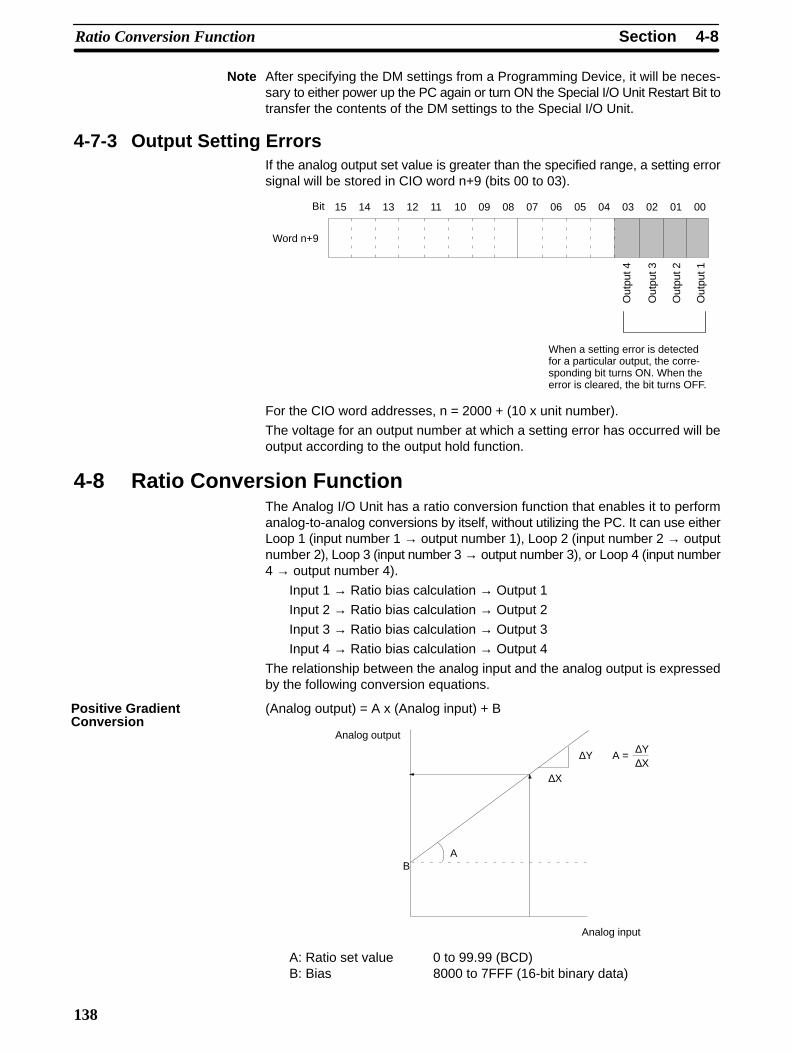
4-8SectionRatio Conversion Function
138
Note After specifying the DM settings from a Programming Device, it will be neces-sary to either power up the PC again or turn ON the Special I/O Unit Restart Bit totransfer the contents of the DM settings to the Special I/O Unit.
4-7-3 Output Setting ErrorsIf the analog output set value is greater than the specified range, a setting errorsignal will be stored in CIO word n+9 (bits 00 to 03).
15 14 13 12 11 10 09 08 07 06 05 04 03 02 01 00Bit
Out
put 2
Out
put 1
Word n+9
When a setting error is detectedfor a particular output, the corre-sponding bit turns ON. When theerror is cleared, the bit turns OFF.
Out
put 4
Out
put 3
For the CIO word addresses, n = 2000 + (10 x unit number).
The voltage for an output number at which a setting error has occurred will beoutput according to the output hold function.
4-8 Ratio Conversion FunctionThe Analog I/O Unit has a ratio conversion function that enables it to performanalog-to-analog conversions by itself, without utilizing the PC. It can use eitherLoop 1 (input number 1 → output number 1), Loop 2 (input number 2 → outputnumber 2), Loop 3 (input number 3 → output number 3), or Loop 4 (input number4 → output number 4).
Input 1 → Ratio bias calculation → Output 1
Input 2 → Ratio bias calculation → Output 2
Input 3 → Ratio bias calculation → Output 3
Input 4 → Ratio bias calculation → Output 4
The relationship between the analog input and the analog output is expressedby the following conversion equations.
(Analog output) = A x (Analog input) + B
BA
Analog output
Analog input
∆X
∆Y A =∆Y∆X
A: Ratio set value 0 to 99.99 (BCD)B: Bias 8000 to 7FFF (16-bit binary data)
Positive GradientConversion

4-8SectionRatio Conversion Function
139
The following example is for an I/O range of –10 to 10 V.
Constant A: 0050 (0.5)Constant B: 0190 (2.0 V)
Analog input: –10 to 10 VAnalog output = 0.5 (–10 to 10 V) + 2.0 V
= –3.0 to 7.0 V
(Analog output) = F – A x (Analog input) + B
F+BA
Analog output
Analog input
∆X
∆Y
A =∆Y∆X
F: Output range maximum valueA: Ratio set value 0 to 99.99 (BCD)B: Bias 8000 to 7FFF (16-bit binary data)
The following example is for an I/O range of 0 to 10 V.
Constant A: 1000 (10.0)Constant B: 0068 (0.5 V)F: 10 V (output range maximum value)
Analog input: 0 to 1 VAnalog output = 10 V – 10 (0 to 1 V) + 0.5 V
= 10.5 to 0.5 V
To specify the use of Loop 1 to Loop 4 and their I/O relationships, set bits 08 to 15of DM Area word D (m) as shown in the following diagram.
15 14 13 12 11 10 09 08 07 06 05 04 03 02 01 00Bit
D (m)
Loop 2 Loop 1
00: Not used.01: Uses positive gradient conversion.10: Uses negative gradient conversion.11: Same as 10 above.
Loop 4 Loop 3
The response time of ratio conversion (input-to-output conversion) is 0.7 ms.
For the DM word addresses, m = 20000 + (100 x unit number).
Negative GradientConversion
Specifying RatioConversion Function

4-8SectionRatio Conversion Function
140
The ratio set value (A) and the bias (B) are set in the DM words from D (m+10) toD (m+17).
DM word Function Set value
D (m+10) Loop 1 (input 1 → output 1), A constant
BCD 0 to 9999 (0.00 to 99.99;unit: 0.01)
D (m+11) Loop 1 (input 1 → output 1), B constant
16-bit binary data
D (m+12) Loop 2 (input 2 → output 2), A constant
BCD 0 to 9999 (0.00 to 99.99;unit: 0.01)
D (m+13) Loop 2 (input 2 → output 2), B constant
16-bit binary data
D (m+14) Loop 3 (input 3 → output 3), A constant
BCD 0 to 9999 (0.00 to 99.99;unit: 0.01)
D (m+15) Loop 3 (input 3 → output 3), B constant
16-bit binary data
D (m+16) Loop 4 (input 4 → output 4), A constant
BCD 0 to 9999 (0.00 to 99.99;unit: 0.01)
D (m+17) Loop 4 (input 4 → output 4), B constant
16-bit binary data
For the DM word addresses, m = 20000 + (100 x unit number).
Note 1. After making the DM settings from a Programming Device, it will be neces-sary to either power up the PC again or turn ON the Special I/O Unit RestartBit to transfer the contents of the DM settings to the Special I/O Unit. Fordetails regarding the Special I/O Unit Restart Bit, refer to 4-10-4 RestartingSpecial I/O Units.
2. The calculation results will be output in digital values to word n+5 (Loop 1),word n+6 (Loop 2), word n+7 (Loop 3). and word n+8 (Loop 4).
3. If an input cable is disconnected, the calculation value will become 0000,and the analog output value will be output according to the output hold func-tion.
4. If the output value exceeds the specified signal range due to the ratio con-version of the digital input value, the calculation result and analog output willbe given as the lower or upper-limit value.
Specifying Ratio SetValue and Bias

4-9SectionAdjusting Offset and Gain
141
4-9 Adjusting Offset and Gain
4-9-1 Adjustment Mode Operational FlowThe adjustment mode enables the input or output of the connected devices to becalibrated. Refer to 2-7 Adjusting Offset and Gain and 3-7 Adjusting Offset andGain for details of input and output functions. The following diagram shows theflow of operations when using the adjustment mode for adjusting offset and gain.
Change the operation mode switch on the rear panel of the Unit.
Turn ON the PC.
When adjusting another I/O number
When adjusting the same I/O number
Set the I/O number.
Offset adjustment
Offset Bit ON (Bit 0 of CIO wordn+1 turns ON.)
Samplinginput
(Add inputs so thatconversion valuebecomes 0.)
Set Bit ON (Bit 4 of CIO wordn+1 turns ON.)
Turn OFF power to the PC.
Change the operation mode switch on the rear panel of the Unit.
Set the operation mode switch to normal mode.
Set the operation mode switch to adjustment mode.
The ADJ indicator will flash while in adjustment mode.
Start up the PC in PROGRAM mode.
Write the I/O number to be adjustedin the rightmost byte of CIO word n.
Gain adjustment
Gain Bit ON (Bit 1 of CIO wordn+1 turns ON.)
Adjustmentvalue setting
(Bits 2 and 3 ofCIO word n+1turn ON.)
Input adjustment Output adjustment
Set Bit ON (Bit 4 of CIO wordn+1 turns ON.)
(Add inputs so thatconversion value ismaximized.)
Samplinginput
Adjustmentvalue setting
(Bits 2 and 3 ofCIO word n+1turn ON.)
Input adjustment Output adjustment

!
!
!
4-9SectionAdjusting Offset and Gain
142
Caution Be sure to turn OFF the power to the PC before changing the setting of theoperation mode switch.
Caution Set the PC to PROGRAM mode when using the Analog I/O Unit in adjustmentmode. If the PC is in MONITOR mode or RUN mode, the Analog I/O Unit will stopoperating, and the input and output values that existed immediately before thisstoppage will be retained.
Caution Always perform adjustments in conjunction with offset and gain adjustments.
Note Input adjustments can be performed more accurately in conjunction with meanvalue processing.
4-9-2 Input Offset and Gain Adjustment Procedures
To specify the input number to be adjusted, write the value to the rightmost byteof CIO word n as shown in the following diagram.
(Rightmost)(Leftmost)
Word n
Input to be adjusted (1 to 4)I/O specification2: Input (fixed)
--- ---
For the CIO word addresses, n = 2000 + (10 x unit number).
The following example uses input number 1 adjustment for illustration. (The unitnumber is 0.)
CLR
SHIFTCH
*DM2
C0
A0
A0
AMON
CHG
2C
1B
WRITE
The CIO word (n+1) bits shown in the following diagram are used for adjustingoffset and gain.
15 14 13 12 11 10 09 08 07 06 05 04 03 02 01 00Bit
Word n+1
Cle
ar B
it
Set
Bit
Gai
n B
it
Offs
et B
it
Specifying Input Numberto be Adjusted
Bits Used for AdjustingOffset and Gain

4-9SectionAdjusting Offset and Gain
143
The procedure for adjusting the analog input offset is explained below. As shownin the following diagram, the offset is adjusted by sampling inputs so that theconversion value becomes 0.
10 V0
0FA0
Offset adjustment input range
Input signal range:0 to 10 V
The following example uses input number 1 adjustment for illustration. (The unitnumber is 0.)
1, 2, 3... 1. Turn ON bit 00 (the Offset Bit) of CIO word n+1. (Hold the ON status.)
CLR
SHIFTCONT
#2
C0
A0
A1
B0
A0
AMON
SET
The analog input’s digital conversion values while the Offset Bit is ON will bemonitored in CIO word n+8.
2. Check whether the input devices are connected.
A6
A6 +
–
+
–
Voltage input
Input 1
Current input
Input 1
For current input, check that the voltage/current switch is ON.
A7
A8
A7
A8
Offset Adjustment

!
!
4-9SectionAdjusting Offset and Gain
144
3. Input the voltage or current so that the conversion value becomes 0000. Thefollowing table shows the offset adjustment voltages and currents to beinput according to the input signal range.
Input signal range Input range Word (n+8) monitoringvalue
0 to 10 V –0.5 to 0.5 V FF38 to 00C8
–10 to 10 V –1.0 to 1.0 V
1 to 5 V 0.8 to 1.2 V
0 to 5 V –0.25 to 0.25 V
4 to 20 mA 3.2 to 4.8 mA
4. After inputting the voltage or current so that the conversion value for theanalog input terminal is 0000, turn ON bit 04 (the Set Bit) of CIO word n+1,and then turn it OFF again.
SHIFTCONT
#2
C0
A0
A1
B0
A4
EMON
SET
RESET
While the Offset Bit is ON, the offset value will be saved to the Unit’sEEPROM when the Set Bit turns ON.
5. To finish the offset adjustment, turn OFF bit 00 (the Offset Bit) of CIO wordn+1.
SHIFTCONT
#2
C0
A0
A1
B0
A0
AMON
RESET
Caution Do not turn OFF the power supply or restart the Unit while the Set Bit is ON (datais being written to the EEPROM). Otherwise, illegal data may be written in theUnit’s EEPROM and “EEPROM Errors” may occur when the power supply isturned ON or when the Unit is restarted, causing a malfunction.
Caution When making adjustments, be sure to perform both the offset adjustment andgain adjustment at the same time.
Note 1. The EEPROM can be overwritten 50,000 times.
2. While the Offset Bit or the Gain Bit is ON, the conversion data at that time willbe displayed in word n+8.If the Offset Bit or the Gain Bit is OFF, the value immediately prior to turningthe bit OFF will be held.

4-9SectionAdjusting Offset and Gain
145
The procedure for adjusting the analog input gain is explained below. As shownin the following diagram, the gain is adjusted by sampling inputs so that the con-version value is maximized.
10 V0
0FA0
Input signal range:0 to 10 V
Gain adjustment input range
The following example uses input number 1 adjustment for illustration. (The unitnumber is 0.)
1, 2, 3... 1. Turn ON bit 01 (the Gain Bit) of CIO word n+1. (Hold the ON status.)
SHIFTCONT
#2
C0
A0
A1
B0
A1
BMON
SET
The analog input’s digital conversion values while the Gain Bit is ON will bemonitored in CIO word n+8.
2. Check whether the input devices are connected.
+
–
+
–
Voltage input
Input 1
Current input
Input 1
For current input, check that the voltage/current switch is ON.
A6
A7
A8
A6
A7
A8
Gain Adjustment

!
!
4-9SectionAdjusting Offset and Gain
146
3. Input the voltage or current so that the conversion value is maximized (0FA0or 07D0). The following table shows the the gain adjustment voltages andcurrents to be input according to the input signal range.
Input signal range Input range Word (n+8) monitoringvalue
0 to 10 V 9.5 to 10.5 V 0ED8 to 1068
–10 to 10 V 9.0 to 11.0 V 0708 to 0898
1 to 5 V 4.8 to 5.2 V 0ED8 to 1068
0 to 5 V 4.75 to 5.25 V 0ED8 to 1068
4 to 20 mA 19.2 to 20.8 mA 0ED8 to 1068
4. With the voltage or current having been input so that the conversion valuefor the Analog I/O Unit is maximized (0FA0 or 07D0), turn bit 04 (the Set Bit)of CIO word n+1 ON and then OFF again.
SHIFTCONT
#2
C0
A0
A1
B0
A4
EMON
SET
RESET
While the Gain Bit is ON, the gain value will be saved to the Unit’s EEPROMwhen the Set Bit turns ON.
5. To finish the gain adjustment, turn OFF bit 01 (the Gain Bit) of CIO word n+1.
SHIFTCONT
#2
C0
A0
A1
B0
A1
BMON
RESET
Caution Do not turn OFF the power supply or restart the Unit while the Set Bit is ON (datais being written to the EEPROM). Otherwise, illegal data may be written in theUnit’s EEPROM and “EEPROM Errors” may occur when the power supply isturned ON or when the Unit is restarted, causing a malfunction.
Caution When making adjustments, be sure to perform both the offset adjustment andgain adjustment at the same time.
Note The EEPROM can be overwritten 50,000 times.

!
!
4-9SectionAdjusting Offset and Gain
147
Follow the procedure outlined below to return the offset and gain adjusted val-ues to their default settings.
The following example uses input number 1 adjustment for illustration. (The unitnumber is 0.)
1, 2, 3... 1. Turn ON bit 05 (the Clear Bit) of CIO word n+1. (Hold the ON status.)Regardless of the input value, 0000 will be monitored in CIO word n+8.
SHIFTCONT
#2
C0
A0
A1
B0
A5
FMON
SET
2. Turn bit 04 of CIO word n+1 ON and then OFF again.
SHIFTCONT
#2
C0
A0
A1
B0
A4
EMON
SET
RESET
While the Clear Bit is ON, the adjusted value will be cleared and reset to thedefault offset and gain values when the Set Bit turns ON.
3. To finish the clearing of adjusted values, turn OFF bit 05 (the Clear Bit) ofCIO word n+1.
SHIFTCONT
#2
C0
A0
A1
B0
A5
FMON
RESET
Caution Do not turn OFF the power supply or restart the Unit while the Set Bit is ON (datais being written to the EEPROM). Otherwise, illegal data may be written in theUnit’s EEPROM and “EEPROM Errors” may occur when the power supply isturned ON or when the Unit is restarted, causing a malfunction.
Caution When making adjustments, be sure to perform both the offset adjustment andgain adjustment at the same time.
Note The EEPROM can be overwritten 50,000 times.
Clearing Offset and GainAdjusted Values

4-9SectionAdjusting Offset and Gain
148
4-9-3 Output Offset and Gain Adjustment ProceduresTo specify the output number to be adjusted, write the value to the rightmost byteof CIO word n as shown in the following diagram.
(Rightmost)(Leftmost)
Word n
Output to be adjusted (1 to 4)I/O specification1: Output (fixed)
--- ---
For the CIO word addresses, n = 2000 + 10 x unit number.The following example uses output number 1 adjustment for illustration. (Theunit number is 0.)
CLR
SHIFTCH
*DM2
C0
A0
A0
AMON
CHG
1B
1B
WRITE
The CIO word n+1 bits shown in the following diagram are used for adjustingoffset and gain.
15 14 13 12 11 10 09 08 07 06 05 04 03 02 01 00Bit
Word n+1
Cle
ar B
it
Set
Bit
Gai
n B
it
Offs
et B
it
Up
Bit
Dow
n B
it
The procedure for adjusting the analog output offset is explained below. Asshown in the following diagram, the set value is adjusted so that the analog out-put reaches the standard value (0V/1V).
10 V
00FA0
Offset adjustment output range
Output signal range:0 to 10 V
Specifying OutputNumber to be Adjusted
Bits Used for AdjustingOffset and Gain
Offset Adjustment

4-9SectionAdjusting Offset and Gain
149
The following example uses output number 1 adjustment for illustration. (Theunit number is 0.)
1, 2, 3... 1. Turn ON bit 00 (the Offset Bit) of CIO word n+1. (Hold the ON status.)
CLR
SHIFTCONT
#2
C0
A0
A1
B0
A0
AMON
SET
2. Check whether the output devices are connected.
A1
A2
Voltage output
Output 1
3. Monitor CIO word n+8 and check the set value while the Offset Bit is ON.
CLR
SHIFTCH
*DM2
C0
A0
A8 MON
4. Change the set value so that the output voltage are as shown in the followingtable. The data can be set within the indicated ranges.
Output signal range Possible outputvoltage/current
adjustment
Output range
0 to 10 V –0.5 to 0.5 V FF38 to 00C8
–10 to 10 V –1.0 to 1.0 V
1 to 5 V 0.8 to 1.2 V
0 to 5 V –0.25 to 0.25 V
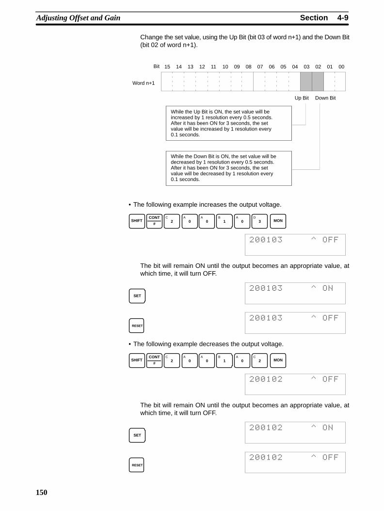
4-9SectionAdjusting Offset and Gain
150
Change the set value, using the Up Bit (bit 03 of word n+1) and the Down Bit(bit 02 of word n+1).
15 14 13 12 11 10 09 08 07 06 05 04 03 02 01 00Bit
Up Bit Down Bit
While the Up Bit is ON, the set value will beincreased by 1 resolution every 0.5 seconds.After it has been ON for 3 seconds, the setvalue will be increased by 1 resolution every0.1 seconds.
While the Down Bit is ON, the set value will bedecreased by 1 resolution every 0.5 seconds.After it has been ON for 3 seconds, the setvalue will be decreased by 1 resolution every0.1 seconds.
Word n+1
• The following example increases the output voltage.
SHIFTCONT
#2
C0
A0
A1
B0
A3
DMON
The bit will remain ON until the output becomes an appropriate value, atwhich time, it will turn OFF.
SET
RESET
• The following example decreases the output voltage.
SHIFTCONT
#2
C0
A0
A1
B0
A2
CMON
The bit will remain ON until the output becomes an appropriate value, atwhich time, it will turn OFF.
SET
RESET

!
!
4-9SectionAdjusting Offset and Gain
151
5. Check the 0-V/1-V output, and then turn bit 04 (the Set Bit) of CIO word n+1ON and then OFF again.
SHIFTCONT
#2
C0
A0
A1
B0
A4
EMON
SET
RESET
While the Offset Bit is ON, the offset value will be saved to the Unit’sEEPROM when the Set Bit turns ON.
6. To finish the offset adjustment, turn OFF bit 00 (the Offset Bit) of CIO wordn+1.
SHIFTCONT
#2
C0
A0
A1
B0
A0
AMON
SET
Caution Do not turn OFF the power supply or restart the Unit while the Set Bit is ON (datais being written to the EEPROM). Otherwise, illegal data may be written in theUnit’s EEPROM and “EEPROM Errors” may occur when the power supply isturned ON or when the Unit is restarted, causing a malfunction.
Caution When making adjustments, be sure to perform both the offset adjustment andgain adjustment at the same time.
Note The EEPROM can be overwritten 50,000 times.
The procedure for adjusting the analog output gain is explained below. As shownin the following diagram, the set value is adjusted so that the analog output ismaximized (to 10V/5V).
10 V
00FA0
Output signal range:0 to 10 V
Gain adjustment output range
Gain Adjustment

4-9SectionAdjusting Offset and Gain
152
The following example uses output number 1 adjustment for illustration. (Theunit number is 0.)
1, 2, 3... 1. Turn ON bit 01 (the Gain Bit) of CIO word n+1. (Hold the ON status.)
CLR
SHIFTCONT
#2
C0
A0
A1
B0
A1
BMON
SET
2. Check whether the output devices are connected.
A1
A2
Voltage output
Output 1
3. Monitor CIO word n+8 and check the set value while the Gain Bit is ON.
CLR
SHIFTCH
*DM2
C0
A0
A8 MON
4. Change the set value so that the output voltage is as shown in the followingtable. The data can be set within the indicated ranges.
Output signal range Possible outputvoltage/current
adjustment
Output range
0 to 10 V 9.5 to 10.5 V 0ED8 to 1068
–10 to 10 V 9.0 to 11.0 V 0708 to 0898
1 to 5 V 4.8 to 5.2 V 0ED8 to 1068
0 to 5 V 4.75 to 5.25 V 0ED8 to 1068

4-9SectionAdjusting Offset and Gain
153
Change the set value, using the Up Bit (bit 03 of word n+1) and the Down Bit(bit 02 of word n+1).
15 14 13 12 11 10 09 08 07 06 05 04 03 02 01 00Bit
Up Bit Down Bit
While the Up Bit is ON, the set value will beincreased by 1 resolution every 0.5 seconds.After it has been ON for 3 seconds, the setvalue will be increased by 1 resolution every0.1 seconds.
While the Down Bit is ON, the set value will bedecreased by 1 resolution every 0.5 seconds.After it has been ON for 3 seconds, the setvalue will be decreased by 1 resolution every0.1 seconds.
Word n+1
• The following example increases the output voltage.
SHIFTCONT
#2
C0
A0
A1
B0
A3
DMON
The bit will remain ON until the output voltage becomes an appropriatevalue, at which time, the output will turn OFF.
SET
RESET
• The following example decreases the output voltage.
SHIFTCONT
#2
C0
A0
A1
B0
A2
CMON
The bit will remain ON until the output voltage becomes an appropriatevalue, at which time, the output will turn OFF.
SET
RESET

!
!
4-9SectionAdjusting Offset and Gain
154
5. Check the 10V/5V output, and then turn bit 04 (the Set Bit) of CIO word n+1ON and then OFF again.
SHIFTCONT
#2
C0
A0
A1
B0
A4
EMON
SET
RESET
While the Gain Bit is ON, the gain value will be saved to the Unit’s EEPROMwhen the Set Bit turns ON.
6. To finish the gain adjustment, turn OFF bit 01 (the Gain Bit) of CIO word n+1.
SHIFTCONT
#2
C0
A0
A1
B0
A1
BMON
RESET
Caution Do not turn OFF the power supply or restart the Unit while the Set Bit is ON (datais being written to the EEPROM). Otherwise, illegal data may be written in theUnit’s EEPROM and “EEPROM Errors” may occur when the power supply isturned ON or when the Unit is restarted, causing a malfunction.
Caution When making adjustments, be sure to perform both the offset adjustment andgain adjustment at the same time.
Note The EEPROM can be overwritten 50,000 times.
Follow the procedure outlined below to return the offset and gain adjusted val-ues to their default settings.
The following example uses output number 1 adjustment for illustration. (Theunit number is 0.)
1, 2, 3... 1. Turn ON bit 05 (the Clear Bit) of CIO word n+1. (Hold the ON status.)Regardless of the set value, 0000 will be monitored in CIO word n+8.
SHIFTCONT
#2
C0
A0
A1
B0
A5
FMON
SET
Clearing Offset and GainAdjusted Values

!
4-9SectionAdjusting Offset and Gain
155
2. Turn bit 04 of CIO word n+1 ON and then OFF again.
SHIFTCONT
#2
C0
A0
A1
B0
A4
EMON
SET
RESET
While the Clear Bit is ON, the adjusted value will be cleared and reset to thedefault offset and gain values when the Set Bit turns ON.
3. To finish the clearing of adjusted values, turn OFF bit 05 (the Clear Bit) ofCIO word n+1.
SHIFTCONT
#2
C0
A0
A1
B0
A5
FMON
RESET
Caution Do not turn OFF the power supply or restart the Unit while the Set Bit is ON (datais being written to the EEPROM). Otherwise, illegal data may be written in theUnit’s EEPROM and “EEPROM Errors” may occur when the power supply isturned ON or when the Unit is restarted, causing a malfunction.
Note The EEPROM can be overwritten 50,000 times.

4-10SectionHandling Errors and Alarms
156
4-10 Handling Errors and Alarms
4-10-1 Indicators and Error Flowchart
If an alarm or error occurs in the Analog I/O Unit, the ERC or ERH indicators onthe front panel of the Unit will light.
Front panel of Unit
RUN
ERC
ADJ
ERH
LED Meaning Indicator Operating statusRUN Operating Lit Operating in normal mode.(green) Not lit Unit has stopped exchanging data with
the CPU Unit.ERC (red) Unit has
detected anerror
Lit Alarm has occurred (such asdisconnection detection) or initialsettings are incorrect.
Not lit Operating normally.
ADJ(yellow)
Adjusting Flashing Operating in offset/gain adjustmentmode.
Not lit Other than the above.
ERH (red) Error in theCPU Unit
Lit Error has occurred during dataexchange with the CPU Unit.
Not lit Operating normally.
Use the following procedure for troubleshooting Analog I/O Unit errors.
Error occurs.
Is the ERC indicatorlit?
Refer to 4-10-5Troubleshooting.
Yes
No
Is the RUN indicatorlit?
Yes
No
Alarm has occurred at the Analog I/O Unit.(Refer to 4-10-2 Alarms Occurring at the Analog I/O Unit.)
Check whether the initial settings for the Analog I/O Unitare set correctly. (Refer to 4-10-2 Alarms Occurring at theAnalog I/O Unit.)
Is the ERH indicatorlit?
Yes
No
Is the RUN indicatorlit?
Yes
No
Error detected by CPU Unit(Refer to 4-10-3 Errors in the CPU Unit.)
Check whether the unit number is set correctly. (Refer to 4-10-3 Errors in the CPU Unit.)
Indicators
TroubleshootingProcedure

4-10SectionHandling Errors and Alarms
157
4-10-2 Alarms Occurring at the Analog I/O UnitWhen an alarm occurs at the Analog I/O Unit, the ERC indicator lights and theAlarm Flags are stored in bits 08 to 15 of CIO word n+9.
15 14 13 12 11 10 09 08 07 06 05 04 03 02 01 00Bit
Word n+9
DisconnectionDetection Flags
(See 4-6-4 InputDisconnectionDetection Function.)
Output setting errors
(See 4-7-3 OutputSetting Errors.)
Alarm Flags
For the CIO word addresses, n = 2000 + (10 x unit number).
ERC and RUN Indicators: Lit
RUN
ERC ERH
: Lit
: Not lit
The ERC and RUN indicators will be lit when an error occurs while the Unit isoperating normally. The following alarm flags will turn ON in CIO word n+9.These alarm flags will turn OFF automatically when the error is cleared.
Word n + 9 Alarm flag Error contents I/O status Countermeasure
Bits 00 to 03 Output SetValue Error
The output setting range hasbeen exceeded.
Output valueset by outputhold function.
Correct the set value.
Bits 04 to 07 DisconnectionDetection
A disconnection was detected.(See note.)
Conversiondata becomes0000.
Check the rightmost byte ofCIO word n+9. The inputs forbits that are ON may bedisconnected. Restore anydisconnected inputs.
Bit 14 (Adjustmentmode)
EEPROMWriting Error
An EEPROM writing error hasoccurred while in adjustmentmode.
Holds theoutput statusimmediatelyprior to theerror.
Turn the Set Bit OFF, ON, andOFF again.
If the error persists even afterthe reset, replace the AnalogI/O Unit.
Note Disconnection detection operates for input numbers used with a range of 1 to 5 V(4 to 20 mA).

4-10SectionHandling Errors and Alarms
158
ERC Indicator and RUN Indicator: Lit, ADJ Indicator: Flashing
RUN
ERC ERH
ADJ
: Lit
: Flashing
: Not lit
This alarm will occur in the case of incorrect operation while in the adjustmentmode. In adjustment mode, the Adjustment Mode ON Flag will turn ON in bit 15of CIO word n+9.
Word n + 9 Alarm flag Error contents I/O status Countermeasure
Bit 12 (Adjustmentmode)
Input ValueAdjustmentRangeExceeded
In adjustment mode, offset orgain cannot be adjustedbecause input value is out ofthe permissible range foradjustment.
Conversiondatacorrespondingto the inputsignal ismonitored inword n+8.
If making the adjustment bymeans of a connected inputdevice, first adjust the inputdevice before adjusting theAnalog I/O Unit.
Bit 13 (Adjustmentmode)
I/O NumberSetting Error
In adjustment mode,adjustment cannot beperformed because thespecified input or outputnumber is not set for use orbecause the wrong input oroutput number is specified.
Holds thevaluesimmediatelyprior to theerror. No data ischanged.
Check whether the word n inputor output number to beadjusted is set from 11 to 14, or21 to 24.
Check whether the input oroutput number to be adjusted isset for use by means of the DMsetting.
Bit 15 only ON (AdjustmentMode)
PC Error
The PC is in either MONITORor RUN mode while the AnalogI/O Unit is operating inadjustment mode.
Holds thevaluesimmediatelyprior to theerror. No data ischanged.
Detach the Unit. Switch therear panel DIP switch pin toOFF. Restart the Unit in normalmode.
Note When a PC error occurs in the adjustment mode, Unit operations will stop oper-ating. (The input and output values immediately prior to the error will be held.)
ERC Indicator: Lit, RUN Indicator: Not Lit
RUN
ERC ERH
: Lit
: Not lit
The ERC indicator will be lit when the initial settings for the Analog I/O Unit arenot set correctly. The alarm flags for the following errors will turn ON in CIO wordn+9. These alarm flags will turn OFF when the error is cleared and the Unit isrestarted, or the Special I/O Unit Restart Bit is turned ON and then OFF again.
Word n + 9 Alarm flag Error contents I/O status Countermeasure
Bit 08 RatioConversion UseSetting Error
The I/O number for the ratioconversion function has beenset to be not used.
Conversiondoes not startand data
Set the I/O number for use.
Bit 09 Ratio Set ValueError
A number outside of the 0 to9999 BCD range has beenspecified for the ratio set value.
becomes 0000. Specify a number from 0 to9999 BCD.
Bit 10 Output HoldSetting Error
The wrong output status forwhen conversion is stoppedhas been specified.
Specify a number from 0000 to0002.
Bit 11 Mean ValueProcessingSetting Error
The wrong number ofsamplings has been specifiedfor mean processing.
Specify a number from 0000 to0006.

4-10SectionHandling Errors and Alarms
159
4-10-3 Errors in the CPU Unit
When errors occur in the CPU Unit or I/O bus, and I/O refresh with the Special I/OUnit is not performed correctly resulting in the Analog I/O Unit malfunctioning,the ERH indicator will be lit.
ERH and RUN Indicators: Lit
RUN
ERC ERH
: Lit
: Not lit
The ERH and RUN indicators will be lit if an error occurs in the I/O bus causing aWDT (watchdog timer) error in the CPU Unit, resulting in incorrect I/O refreshwith the Analog I/O Unit.
Turn ON the power supply again or restart the system.For further details, refer to CS1-series CS1G/H-CPU-E ProgrammableControllers Operation Manual (W339).
Error Error contents Input condition Output condition
I/O bus error Error has occurred duringdata exchange with theCPU Unit.
Conversion data becomes0000.
Depends on the output holdfunction.
CPU Unit monitoring error(see note)
No response from CPU Unitduring fixed period.
Maintains the conditionexisting before the error.
Maintains the conditionexisting before the error.
CPU Unit WDT error Error has been generated inCPU Unit.
Changes to undefined state. Depends on the output holdfunction.
Note No error will be detected by the CPU Unit or displayed on the Programming Con-sole, because the CPU Unit is continuing operation.
ERH Indicator: Lit, RUN Indicator: Not Lit
RUN
ERC ERH
: Lit
: Not lit
The unit number for the Analog I/O Unit has not been set correctly.
Error Error contents Input condition Output condition
Duplicate Unit Number The same unit number hasbeen assigned to more thanone Unit or the unit numberwas set to a value otherthan 00 to 95.
Conversion does not startand data becomes 0000.
The output value will be 0 V.
Special I/O Unit SettingError
The Special I/O Unitsregistered in the I/O tableare different from the onesactually mounted.
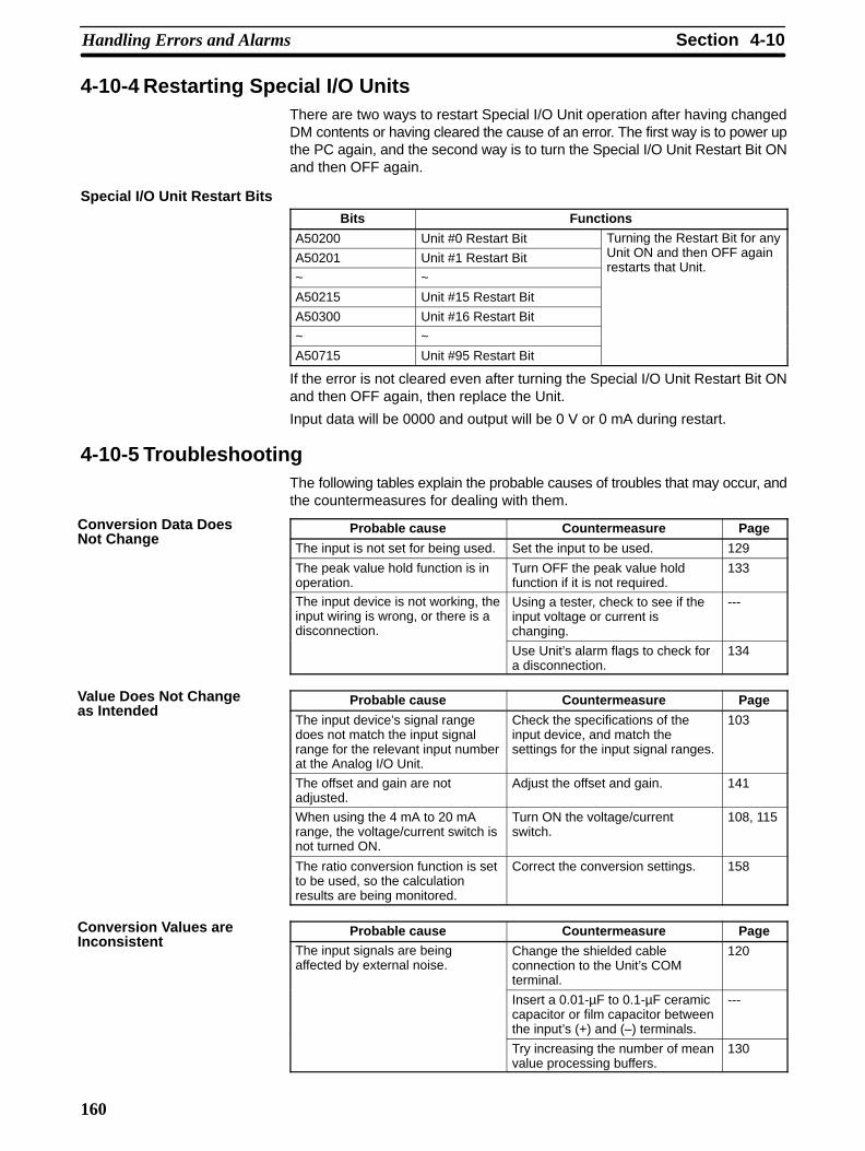
4-10SectionHandling Errors and Alarms
160
4-10-4 Restarting Special I/O UnitsThere are two ways to restart Special I/O Unit operation after having changedDM contents or having cleared the cause of an error. The first way is to power upthe PC again, and the second way is to turn the Special I/O Unit Restart Bit ONand then OFF again.
Special I/O Unit Restart Bits
Bits Functions
A50200 Unit #0 Restart Bit Turning the Restart Bit for any
A50201 Unit #1 Restart Bit Unit ON and then OFF again
~ ~restarts that Unit.
A50215 Unit #15 Restart Bit
A50300 Unit #16 Restart Bit
~ ~
A50715 Unit #95 Restart Bit
If the error is not cleared even after turning the Special I/O Unit Restart Bit ONand then OFF again, then replace the Unit.
Input data will be 0000 and output will be 0 V or 0 mA during restart.
4-10-5 TroubleshootingThe following tables explain the probable causes of troubles that may occur, andthe countermeasures for dealing with them.
Probable cause Countermeasure Page
The input is not set for being used. Set the input to be used. 129
The peak value hold function is inoperation.
Turn OFF the peak value holdfunction if it is not required.
133
The input device is not working, theinput wiring is wrong, or there is adisconnection.
Using a tester, check to see if theinput voltage or current ischanging.
---
Use Unit’s alarm flags to check fora disconnection.
134
Probable cause Countermeasure Page
The input device’s signal rangedoes not match the input signalrange for the relevant input numberat the Analog I/O Unit.
Check the specifications of theinput device, and match thesettings for the input signal ranges.
103
The offset and gain are notadjusted.
Adjust the offset and gain. 141
When using the 4 mA to 20 mArange, the voltage/current switch isnot turned ON.
Turn ON the voltage/currentswitch.
108, 115
The ratio conversion function is setto be used, so the calculationresults are being monitored.
Correct the conversion settings. 158
Probable cause Countermeasure Page
The input signals are beingaffected by external noise.
Change the shielded cableconnection to the Unit’s COMterminal.
120
Insert a 0.01-µF to 0.1-µF ceramiccapacitor or film capacitor betweenthe input’s (+) and (–) terminals.
---
Try increasing the number of meanvalue processing buffers.
130
Conversion Data DoesNot Change
Value Does Not Changeas Intended
Conversion Values areInconsistent

4-10SectionHandling Errors and Alarms
161
Probable Cause Countermeasure Page
The output is not set for beingused.
Set the output to be used. 135
The output hold function is inoperation.
Turn ON the Output ConversionEnable Bit.
137
The conversion value is set outsideof the permissible range.
Set the data within the range. 105, 135
Probable Cause Countermeasure Page
The output signal range setting iswrong.
Correct the output signal rangesetting.
135
The I/O specifications of the outputdevice do not match those of theAnalog I/O Unit (e.g., input signalrange, input impedance).
Change the output device. 101
The offset or gain is not adjusted. Adjust the offset or gain. 141
The ratio conversion function is setto be used.
Correct the conversion settings. 138
Probable Cause Countermeasure Page
The output signals are beingaffected by external noise.
Try changing the shielded cableconnection (e.g., the grounding atthe output device).
---
Analog Output Does NotChange
Output Does Not Changeas Intended
Outputs are Inconsistent

163
Appendix ADimensions
CS1W-AD041/081CS1W-DA08V/08C/041CS1W-MAD44
101
12635
130
Terminal Block Dimensions
Terminal size: M3

165
Appendix BSample Programs
Obtaining Analog Input Conversion ValuesThis is a program for obtaining the Analog Input Unit’s input conversion values. Individual input values areobtained by MOV(021) when their Disconnection Detection Flags are OFF.
Unit SettingsItem Setting contents Actual settings
Unit CS1W-AD081 ---
Unit number #0 Unit number switch: 00
Operation mode Normal mode Back-panel DIP switch: All OFF
Input number Inputs 1 to 8 used D20000 = 00FF
Input signal range All input numbers, 1 to 5 V D20001 = AAAA
Program Example
200900
MOV(021)
2001
D00000200901
MOV(021)
2002
D00001
Conversion value
Conversion value
200907
MOV(021)
2008
D00007
Conversion value
Input 1 Disconnection Detection Flag
Input 2 Disconnection Detection Flag
Input 8 Disconnection Detection Flag
Writing Analog Output Set ValuesThis is a program for writing the Analog Output Unit’s output set values.
Item Setting contents Actual settings
Unit CS1W-DA08V ---
Unit number #0 Unit number switch: 00
Operation mode Normal mode Back-panel DIP switch: All OFF
Output number Output 1 used D20000 = 0001
Output signal range Output number 1, 0 to 10 V D20001 = 0001

Appendix BSample Programs
166
Program Example
MOV(021)
D00000
2001
200900
Output Setting Error Flag
Reset condition
Output 1 Setting Error Flag
Set value
Execution condition
Upper and Lower-limit Alarm (Constant Monitoring)Comparisons are made to the upper and lower limits of the A/D conversion values or D/A output values from thebeginning of operation. If they fall outside the specified range, the Alarm Flag will turn ON.
Upper limit
Lower limit
Alarm FlagON
OFF
Unit SettingsItem Setting contents Actual settings
Unit CS1W-AD081 ---
Unit number #0 Unit number switch: 00
Operation mode Normal mode Back-panel DIP switch: All OFF
Input number Input 1 used D20000 = 0001
Input signal range Input number 1, 0 to 10 V D20001 = 0001
Program Example
<
2001
D00000
Operation condition
Conversion value
Lower limit
Alarm Flag
>
2001
D00001
Conversion valueUpper limit

Appendix BSample Programs
167
Upper and Lower-limit Alarm (with Standby Sequence)Comparisons are made to the upper and lower limits of the A/D conversion values or D/A output values after thevalue falls within the range between the upper limit and lower limit following the beginning of operation. If they falloutside the specified range, the Alarm Flag will turn ON.
Upper limit
Lower limit
Alarm FlagON
OFF
Unit SettingsItem Setting contents Actual settings
Unit CS1W-AD081 ---
Unit number #0 Unit number switch: 00
Operation mode Normal mode Back-panel DIP switch: All OFF
Input number Input 1 used D20000 = 0001
Input signal range Input number 1, 0 to 10 V D20001 = 0001
Program Example
KEEP(11)
020001
<
2001
D00000
Operation condition
Conversion valueLower limit
Alarm Flag
>
2001
D00001
Conversion value
Upper limit
020001
020001
2001
D00000
Conversion value
Lower limit
2001
D00001
Conversion valueUpper limit
Operationcondition

Appendix BSample Programs
168
ScalingA/D conversion values are converted according to the linear function calculated from the offset and the values of
X and Y, and retrieved as scaling data.
• The following example uses an input signal range of 1 to 5 V where 1 to 5 V is scaled to 0000 to 0300 (0C to300C).
0315
0300
0000
–0015FF38
0.8 V 1 V
0000 0FA0
5 V
1068
5.2 V
0315(Y)
1068 Hex(X)
Unit Settings
Item Setting contents Actual settings
Unit CS1W-AD081 ---
Unit number #0 Unit number switch: 00
Operation mode Normal mode Back-panel DIP switch: All OFF
Input number Input 1 used D20000 = 0001
Input signal range Input number 1, 1 to 5 V D20001 = 0002
Program Example• Data Flow (Unit Number 0):
Word CIO 2001 (A/D Conversion Value) → D00200 (Scaling Result)
SCL2
2001
D00100
D00200
Execution condition
The value of word CIO 2005 is scaled according to the linear function calculated using the offset (0000 Hex), and
the values of X (1068 Hex) and Y (0315 Hex). The scaled value is then stored in word D00200.
DM Area Settings
D00100: 0000
D00101: 1068
D00102: 0315
Offset
X value
Y value

Appendix BSample Programs
169
Note The value scaled using SCL2(486) is stored as positive or negative BCD data according to the status of theCY (Carry) Flag. To convert the BCD data into signed binary data, use the SCL3(487) instruction.
SCL2
2005
D00100
D00200
SCL3
D00200
D00300
D00400
Execution condition
DM Area Settings
D00300: 0000
D00301: 0200
D00302: 00C8
D00303: 00C8
D00304: FF9C
Offset
X value
Y value
Maximum conversion value
Minimum conversion value
Signed Binary-to-Signed BCD ConversionA/D conversion values (16-bit binary data) are recognized as 4-digit signed binary data, and converted into 8-digitsigned BCD data. When the leftmost bit is 1, the binary data is recognized as a two’s complement. The “signedBCD” data refers to BCD data that is indicated by 7-digit data and 1-digit sign (0: +; F: –).
• Conversion Graph (Horizontal Axis: Input Voltage, Vertical Axis: BCD Data)
00002000
F0002000
10 V (07D0)
–10 V (F830)
00004200
F0002000
–0.5 V (FF38)
10.5 V (1068)
Input signal range: –10 to 10 V Input signal range: 0 to 10 V
Unit SettingsItem Setting contents Actual settings
Unit CS1W-AD081 ---
Unit number #0 Unit number switch: 00
Operation mode Normal mode Back-panel DIP switch: All OFF
Input number Input 1 used D20000 = 0001
Input signal range Input number 1, 0 to 10 V D20001 = 0001

Appendix BSample Programs
170
Program Example• Data Flow (Unit Number 0):
Word 2001 (A/D Conversion Value) → Words 0201 and 0200 (Conversion Result)
ANDW(034)
#8000
D00000
D00002
=ERR
MOV(021)
2001
D00000
MOV(021)
#0000
D00001
NEG (060)
D00000
D00000
MOV(021)
#F000
D00001
BCD(024)
D00000
D00000
XFER(070)
#0002
D00000
0200
Execution condition
16-bit binary data
Clears leftmost word to 0000
Adds 1 and reversesleftmost bit if it is not 0.
Sends F000 to leftmost word ifthe leftmost bit is not 0.
Converts to BCD.
Outputs signed BCD data towords 0200 and 0201.
(1)
(2)
(3)
(1) If the leftmost bit is a 1 (negative number) in 16-bit binary data, the data is reversed and the leftmost wordbecomes F000.
(2) 16-bit binary data is converted to BCD.
(3) Signed BCD data is output to words 0200 and 0201.
Square Root CalculationData expressed as quadratic curves, such as thermocouple inputs, is converted and output to linear data (0000 to4000).
Unit Settings
Item Setting contents Actual settings
Unit CS1W-AD081 ---
Unit number #0 Unit number switch: 00
Operation mode Normal mode Back-panel DIP switch: All OFF
Input number Input 1 used D20000 = 0001
Input signal range Input number 1, 0 to 10 V D20001 = 0001
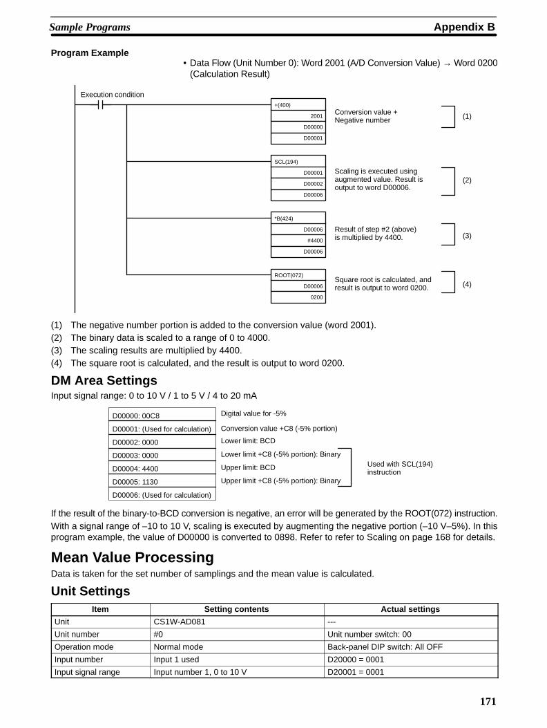
Appendix BSample Programs
171
Program Example• Data Flow (Unit Number 0): Word 2001 (A/D Conversion Value) → Word 0200
(Calculation Result)
+(400)
2001
D00000
D00001
ROOT(072)
D00006
0200
SCL(194)
D00001
D00002
D00006
*B(424)
D00006
#4400
D00006
Execution condition
Conversion value +Negative number
Scaling is executed usingaugmented value. Result isoutput to word D00006.
Result of step #2 (above)is multiplied by 4400.
Square root is calculated, andresult is output to word 0200.
(1)
(2)
(3)
(4)
(1) The negative number portion is added to the conversion value (word 2001).(2) The binary data is scaled to a range of 0 to 4000.(3) The scaling results are multiplied by 4400.(4) The square root is calculated, and the result is output to word 0200.
DM Area SettingsInput signal range: 0 to 10 V / 1 to 5 V / 4 to 20 mA
D00000: 00C8
D00001: (Used for calculation)
D00002: 0000
D00003: 0000
D00004: 4400
D00005: 1130
D00006: (Used for calculation)
Digital value for -5%
Conversion value +C8 (-5% portion)
Lower limit: BCD
Lower limit +C8 (-5% portion): Binary
Upper limit: BCD
Upper limit +C8 (-5% portion): Binary
Used with SCL(194)instruction
If the result of the binary-to-BCD conversion is negative, an error will be generated by the ROOT(072) instruction.With a signal range of –10 to 10 V, scaling is executed by augmenting the negative portion (–10 V–5%). In thisprogram example, the value of D00000 is converted to 0898. Refer to refer to Scaling on page 168 for details.
Mean Value ProcessingData is taken for the set number of samplings and the mean value is calculated.
Unit SettingsItem Setting contents Actual settings
Unit CS1W-AD081 ---
Unit number #0 Unit number switch: 00
Operation mode Normal mode Back-panel DIP switch: All OFF
Input number Input 1 used D20000 = 0001
Input signal range Input number 1, 0 to 10 V D20001 = 0001

Appendix BSample Programs
172
Program Example• Data Flow (Unit Number 0): Word 2001 (AD Conversion Value) → D00001
(Mean Value Result)
AVG(195)
2001
#0064
D00001
Execution condition
Conversion value
Number of samplings
Mean value
LimitIf the output value range is exceeded, the output voltage is held when the Conversion Enable Flag turns OFF.
5 V (03E8)
0 V (0000)
Set value
Actual output value
When program is started
Unit SettingsItem Setting contents Actual settings
Unit CS1W-DA08V ---
Unit number #0 Unit number switch: 00
Operation mode Normal mode Back-panel DIP switch: All OFF
Output number Output 1 used D20000 = 0001
Output signal range All output numbers, 0 to 10 V D20001 = 0001
Output hold function HOLD D20002 = 0001
Program Example
MOV(021)
D00000
2001
Execution condition
Set value
<
2001
D00000
Set valueLower limit
Conversion EnableFlag for output 1
>
2001
D00001
Set value
Upper limit
200000
DM Area Settings
D00001: 0000
D00002: 03E8
Lower limit: 0 V
Upper limit: 5 V
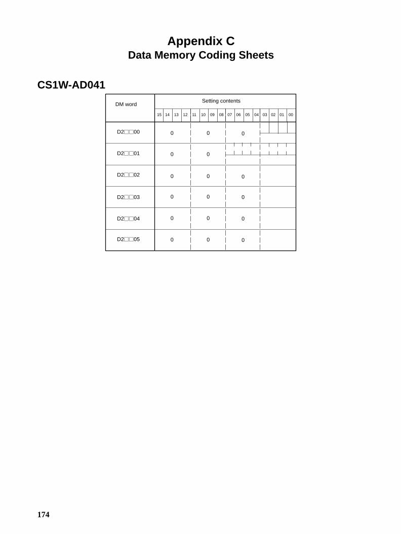
174
Appendix CData Memory Coding Sheets
CS1W-AD041
DM wordSetting contents
D200
D201
D202
D203
D204
D205
0
0
0
0
0
0
0
0
0
0
0
0
14 13 12 11 10 09 08 07 06 05 04 03 02 01 0015
0 0
0 0 0

Appendix CData Memory Coding Sheets
175
DM word Setting contents
15 8 7 0
m
m+1
m+2
m+3
m+4
m+5
Input usedesignation
03 02 01 00
Inpu
t 2
Inpu
t 1
Use Designation
0: Do not use.1: Use
07 06 05 04 03 02 01 00
Inpu
t 2
Inpu
t 1
Signal Range Setting
00: -10 to 10 V01: 0 to 10 V10: 1 to 5 V / 4 to 20 mA (change using voltage/current switch)11: 0 to 5 V
15 12 11 08 07 04 03 00
163 162 161 160
Mean Value Processing Setting
0000: Mean value processing with 2 buffers.0001: No mean value processing0002: Mean value processing with 4 buffers.0003: Mean value processing with 8 buffers.0004: Mean value processing with 16 buffers.0005: Mean value processing with 32 buffers.0006: Mean value processing with 64 buffers.
Input signalrange setting
Inpu
t 4
Inpu
t 3In
put 4
Inpu
t 3
Input 1: Mean value processing setting
Input 2: Mean value processing setting
Input 3: Mean value processing setting
Input 4: Mean value processing setting
Note m=20000+100 x unit number is allocated as the DM number.

Appendix CData Memory Coding Sheets
176
CS1W-AD081
DM wordSetting contents
D200
D201
D202
D203
D204
D205
D206
D207
D208
D209
0
0
0
0
0
0
0
0
0
0
0
0
14 13 12 11 10 09 08 07 06 05 04 03 02 01 0015
0 0
0
0
0
0
0
0
0
0
0
0
0
0

Appendix CData Memory Coding Sheets
177
DM word Setting contents
15 8 7 0
m
m+1
m+2
m+3
m+4
m+5
m+6
m+7
m+8
m+9
Input usedesignation
Input 5: Mean value processing setting
Input 6: Mean value processing setting
07 06 05 04 03 02 01 00
Inpu
t 6
Inpu
t 5
Inpu
t 2
Inpu
t 1
Use Designation
0: Do not use.1: Use
07 06 05 04 03 02 01 00
15 14 13 12 11 10 09 08
Inpu
t 6
Inpu
t 5
Signal Range Setting
00: -10 to 10 V01: 0 to 10 V10: 1 to 5 V / 4 to 20 mA (change using voltage/current switch)11: 0 to 5 V
Inpu
t 2
Inpu
t 1
15 12 11 08 07 04 03 00
163 162 161 160
Mean Value Processing Setting
0000: Mean value processing with 2 buffers.0001: No mean value processing0002: Mean value processing with 4 buffers.0003: Mean value processing with 8 buffers.0004: Mean value processing with 16 buffers.0005: Mean value processing with 32 buffers.0006: Mean value processing with 64 buffers.
Input 7: Mean value processing setting
Input 8: Mean value processing setting
Not used
Input signal range setting
Inpu
t 8
Inpu
t 7
Inpu
t 4
Inpu
t 3
Inpu
t 4
Inpu
t 3
Inpu
t 8
Inpu
t 7
Input 1: Mean value processing setting
Input 2: Mean value processing setting
Input 3: Mean value processing setting
Input 4: Mean value processing setting
Note m=20000+100 x unit number is allocated as the DM number.

Appendix CData Memory Coding Sheets
178
CS1W-DA041
DM wordSetting contents
D200
D201
D202
D203
D204
D205
0
0
0
0
0
0
0
0
0
0
0
0
14 13 12 11 10 09 08 07 06 05 04 03 02 01 0015
0 0
0 0 0

Appendix CData Memory Coding Sheets
179
DM word Setting contents
15 8 7 0
m
m+1
m+2
m+3
m+4
m+5
Output usedesignation
Output 1: Output statuswhen conversion stopped
Output 2: Output statuswhen conversion stopped
03 02 01 00
Out
put 2
Out
put 1
Use Designation
0: Do not use.1: Use
07 06 05 04 03 02 01 00
Signal Range Setting
00: -10 to 10 V01: 0 to 10 V10: 1 to 5 V / 4 to 20 mA11: 0 to 5 V
Out
put 2
Out
put 1
07 04 03 00
161 160
00: CLR (0 or minimum value for each range output)01: HOLD (Hold prior output value.)02: MAX (Output maximum value of range.)
Output Status when Conversion Stopped
Output 3: Output statuswhen conversion stopped
Output 4: Output statuswhen conversion stopped
Output signalrange setting
Out
put 4
Out
put 3
Out
put 4
Out
put 3
Note m=20000+100 x unit number is allocated as the DM number.

Appendix CData Memory Coding Sheets
180
CS1W-DA08V/08C
DM wordSetting contents
D200
D201
D202
D203
D204
D205
D206
D207
D208
D209
0
0
0
0
0
0
0
0
0
0
0
0
14 13 12 11 10 09 08 07 06 05 04 03 02 01 0015
0 0
0
0
0
0
0
0
0
0
0
0
0
0

Appendix CData Memory Coding Sheets
181
DM word Setting contents
15 8 7 0
m
m+1
m+2
m+3
m+4
m+5
m+6
m+7
m+8
m+9
Output usedesignation
Output 1: Output statuswhen conversion stopped
Output 2: Output statuswhen conversion stopped
07 06 05 04 03 02 01 00
Out
put 6
Out
put 5
Out
put 2
Out
put 1
Use Designation
0: Do not use.1: Use
07 06 05 04 03 02 01 00
15 14 13 12 11 10 09 08
Signal Range Setting (not valid for CS1W-DA08C)
00: -10 to 10 V01: 0 to 10 V10: 1 to 5 V11: 0 to 5 V
Out
put 2
Out
put 1
07 04 03 00
161 160
00: CLR (0 or minimum value for each range output)01: HOLD (Hold prior output value.)02: MAX (Output maximum value of range.)
Output Status when Conversion Stopped
Output 3: Output statuswhen conversion stopped
Output 4: Output statuswhen conversion stopped
Output signal range setting
Out
put 8
Out
put 7
Out
put 4
Out
put 3
Out
put 4
Out
put 3
Output 5: Output statuswhen conversion stopped
Output 6: Output statuswhen conversion stopped
Output 7: Output statuswhen conversion stopped
Output 8: Output statuswhen conversion stopped
Out
put 6
Out
put 5
Out
put 8
Out
put 7
Note m=20000+100 x unit number is allocated as the DM number.

Appendix CData Memory Coding Sheets
182
CS1W-MAD44
DM wordSetting contents
D200
D201
D202
D203
D204
D205
D206
D207
D208
D209
D210
D211
D212
D213
D214
D215
D216
D217
0
0
0
0
0
0
0
0
0
0
0
0
14 13 12 11 10 09 08 07 06 05 04 03 02 01 0015

Appendix CData Memory Coding Sheets
183
DM word Setting contents
15 8 7 0
m
m+1
m+2
m+3
m+4
m+5
m+6
m+7
m+8
m+9
m+10
m+11
m+12
m+13
Input usedesignation
Output usedesignation
Output 1: Output statuswhen conversion stopped
Output 2: Output statuswhen conversion stopped
Input 1: Mean value processing setting
Input 2: Mean value processing setting
Loop 1 (input 1 → output 1), A constant
Loop 1 (input 1 → output 1), B constant
Loop 2 (input 2 → output 2), A constant
Loop 2 (input 2 → output 2), B constant
07 06 05 04 03 02 01 00
Inpu
t 2
Inpu
t 1
Out
put 2
Out
put 1
15 14 13 12 11 10 09 08
Loop
2
Loop
1
Use Designation
0: Do not use.1: Use
00: Do not use.01: Positive gradient conversion10: Negative gradient conversion11: Same as the above “00” setting
07 06 05 04 03 02 01 00
15 14 13 12 11 10 09 08
Inpu
t 2
Inpu
t 1
Signal Range Setting
00: -10 to 10 V01: 0 to 10 V10: 1 to 5 V / 4 to 20 mA (4 to 20 mA is for analog input only)11: 0 to 5 V
Out
put 2
Out
put 1
B Constant
16-bit binary data
A Constant0 to 9999 BCD (0.00 to 99.99; unit: 0.01)
07 04 03 00
161 160
00: CLR (0 or minimum value for each range output)01: HOLD (Hold prior output value.)02: MAX (Output maximum value of range.)
Output Status when Conversion Stopped
15 12 11 08 07 04 03 00
163 162 161 160
Mean Value Processing Setting
0000: Mean value processing with 2 buffers.0001: No mean value processing0002: Mean value processing with 4 buffers.0003: Mean value processing with 8 buffers.0004: Mean value processing with 16 buffers.0005: Mean value processing with 32 buffers.0006: Mean value processing with 64 buffers.
m+14
m+15
m+16
m+17
Loop 3 (input 3 → output 3), A constant
Loop 3 (input 3 → output 3), B constant
Loop 4 (input 4 → output 4), A constant
Loop 4 (input 4 → output 4), B constant
Output 3: Output statuswhen conversion stopped
Output 4: Output statuswhen conversion stopped
Input 3: Mean value processing setting
Input 4: Mean value processing setting
Ratio conversionuse designation
Input signalrange setting
Output signalrange setting
Inpu
t 4
Inpu
t 3
Out
put 4
Out
put 3
Loop
4
Loop
3
Out
put 4
Out
put 3
Inpu
t 4
Inpu
t 3
16-bit binary data
Note m=20000+100 x unit number is allocated as the DM number.

185
Index
A–BA constant, Analog I/O Unit, 125, 140
A/D conversion timeAnalog I/O Unit, 101Analog Input Unit, 11
adjustment modeallocations
Analog I/O Unit, 128Analog Input Unit, 34Analog Output Unit, 78
operational flowAnalog I/O Unit, 141Analog Input Unit, 41Analog Output Unit, 84
Alarm FlagsAnalog I/O Unit, 127, 128, 157Analog Input Unit, 34, 35, 50Analog Output Unit, 78, 79, 95
alarmsAnalog I/O Unit, 156Analog Input Unit, 49Analog Output Unit, 94upper and lower limit, 166
B constant, Analog I/O Unit, 125, 140
bias, Analog I/O Unit, 140
Ccircuitry
inputAnalog I/O Unit, 118Analog Input Unit, 25
internalAnalog I/O Unit, 118Analog Input Unit, 25Analog Output Unit, 70
outputAnalog I/O Unit, 118Analog Output Unit, 70
Clear BitAnalog I/O Unit, 128, 142, 148Analog Input Unit, 35, 43Analog Output Unit, 79, 86
componentsAnalog I/O Unit, 114Analog Input Unit, 21Analog Output Unit, 66
configuration, internalAnalog I/O Unit, 118Analog Input Unit, 26Analog Output Unit, 70
conversionsigned binary to signed BCD, 169stopping and starting
Analog I/O Unit, 136Analog Output Unit, 81
timeAnalog Input Unit, 11Analog I/O Unit, 101Analog Output Unit, 57
valuesAnalog I/O Unit, 129, 135Analog Input Unit, 35Analog Output Unit, 79
Conversion Enable BitAnalog I/O Unit, 136Analog Output Unit, 81
DD/A conversion time
Analog I/O Unit, 101Analog Output Unit, 57
data exchangeAnalog I/O Unit, 100, 121Analog Input Unit, 10, 28Analog Output Unit, 56, 72
data memory coding sheets, 174
dimensions, 163Analog I/O Unit, 100Analog Input Unit, 10Analog Output Unit, 56
disconnection, voltage inputAnalog I/O Unit, 119Analog Input Unit, 26
Disconnection Detection Flag, 165Analog I/O Unit, 112Analog Input Unit, 20
DM allocations, contentsAnalog I/O Unit, 124Analog Input Unit, 30Analog Output Unit, 75
Down BitAnalog I/O Unit, 128, 148Analog Input Unit, 35Analog Output Unit, 79, 86
EEC Directives, xv
Index
186
errorsAnalog I/O Unit, 156Analog Input Unit, 49Analog Output Unit, 94CPU Unit, 52, 96, 159UNIT No. DPL ERR
Analog I/O Unit, 123Analog Input Unit, 30Analog Output Unit, 74
external terminalsAnalog I/O Unit, 100Analog Input Unit, 10Analog Output Unit, 56
Ffixed data
allocationsAnalog I/O Unit, 123Analog Input Unit, 30Analog Output Unit, 74
Analog I/O Unit, 121Analog Input Unit, 28Analog Output Unit, 72set values
Analog I/O Unit, 125Analog Input Unit, 31Analog Output Unit, 75
stored valuesAnalog I/O Unit, 125Analog Input Unit, 31Analog Output Unit, 75
functions, 2applications, 7input
Analog I/O Unit, 101Analog Input Unit, 11
other, Analog I/O Unit, 101output
Analog I/O Unit, 101Analog Output Unit, 57
G–Hgain adjustment function, 4
Analog I/O Unit, 141, 145, 151Analog Input Unit, 41, 46Analog Output Unit, 84, 90applications, 7clearing adjusted values
Analog I/O Unit, 147, 154Analog Input Unit, 48Analog Output Unit, 93
setting procedureAnalog I/O Unit, 107Analog Input Unit, 15Analog Output Unit, 60
Gain BitAnalog I/O Unit, 128, 142, 148Analog Input Unit, 35, 43Analog Output Unit, 79, 86
gradient conversionnegative, Analog I/O Unit, 139positive, Analog I/O Unit, 138
high-speed conversion, 2
history buffersAnalog I/O Unit, 130Analog Input Unit, 37
I–L
I/O refresh dataallocations
Analog I/O Unit, 126Analog Input Unit, 32Analog Output Unit, 76
Analog I/O Unit, 121Analog Input Unit, 28Analog Output Unit, 72set values
Analog I/O Unit, 127Analog Input Unit, 34Analog Output Unit, 78
stored valuesAnalog I/O Unit, 127Analog Input Unit, 34Analog Output Unit, 78
I/O tables, creationAnalog I/O Unit, 110Analog Input Unit, 17Analog Output Unit, 63
indicatorsAnalog I/O Unit, 115Analog Input Unit, 22Analog Output Unit, 67errors
Analog I/O Unit, 156Analog Input Unit, 49Analog Output Unit, 94
initial data, settingsAnalog I/O Unit, 110Analog Input Unit, 18Analog Output Unit, 63

Index
187
inputcircuitry
Analog I/O Unit, 118Analog Input Unit, 25
impedanceAnalog I/O Unit, 101Analog Input Unit, 11
numbersAnalog I/O Unit, 129, 142Analog Input Unit, 35, 43
settingsAnalog I/O Unit, 129Analog Input Unit, 35
signal range, 2Analog I/O Unit, 101, 125, 129Analog Input Unit, 11, 31, 36
specificationsAnalog I/O Unit, 101, 103Analog Input Unit, 11, 13
input disconnection detection function, 3Analog I/O Unit, 134Analog Input Unit, 40applications, 7
input functions, block diagramAnalog I/O Unit, 102Analog Input Unit, 12
installation, procedureAnalog I/O Unit, 107Analog Input Unit, 15Analog Output Unit, 60
isolationAnalog I/O Unit, 100Analog Input Unit, 10Analog Output Unit, 56
ladder programsAnalog I/O Unit, 111Analog Input Unit, 19Analog Output Unit, 64
limit, 172
loops, Analog I/O Unit, 139
M–Nmaximum Units
per RackAnalog I/O Unit, 100Analog Input Unit, 10Analog Output Unit, 56
per system, Analog I/O Unit, 100
mean value function, 4applications, 7settings
Analog I/O Unit, 125Analog input Unit, 31
mean value processing, 171Analog I/O Unit, 130Analog Input Unit, 37
mounting
position
Analog I/O Unit, 100
Analog Input Unit, 10
Analog Output Unit, 56
precautions
Analog I/O Unit, 142
Analog Input Unit, 42
Analog Output Unit, 85
restrictions, 5
normal mode, allocations
Analog I/O Unit, 127
Analog Input Unit, 33
Analog Output Unit, 77
O
offset adjustment function, 4
Analog I/O Unit, 141, 143, 148
Analog Input Unit, 41, 44
Analog Output Unit, 84, 87
applications, 7
clearing adjusted values
Analog I/O Unit, 147, 154
Analog Input Unit, 48
Analog Output Unit, 93
setting procedure
Analog I/O Unit, 107
Analog Input Unit, 15
Analog Output Unit, 60
Offset Bit
Analog I/O Unit, 128, 142, 148
Analog Input Unit, 35, 43
Analog Output Unit, 79, 86
operating procedure
Analog I/O Unit, 107
Analog Input Unit, 15
Analog Output Unit, 61
operation mode switch
Analog I/O Unit, 116
Analog Input Unit, 23
Analog Output Unit, 68

Index
188
outputcircuitry
Analog I/O Unit, 118Analog Output Unit, 70
currentAnalog I/O Unit, 101Analog Output Unit, 57
dataAnalog I/O Unit, 101Analog Input Unit, 11
impedanceAnalog I/O Unit, 101Analog Output Unit, 57
numbersAnalog I/O Unit, 135, 148Analog Output Unit, 79, 86
setting errorsAnalog I/O Unit, 138Analog Output Unit, 83
settingsAnalog I/O Unit, 135Analog Output Unit, 79
signal range, 2Analog I/O Unit, 101, 125, 135, 137Analog Output Unit, 57, 75, 80, 82
specificationsAnalog I/O Unit, 101, 105Analog Output Unit, 57, 58
status, 75Analog I/O Unit, 125, 137Analog Output Unit, 82
output functions, block diagramAnalog I/O Unit, 102Analog Output Unit, 58
output hold function, 3Analog I/O Unit, 137Analog Output Unit, 81applications, 7
P
Peak Value Hold BitAnalog I/O Unit, 133Analog Input Unit, 40
peak value hold function, 3Analog I/O Unit, 133Analog Input Unit, 39applications, 7
power consumptionAnalog I/O Unit, 100Analog Input Unit, 10Analog Output Unit, 56
Power Supply Units, 5
precautions, 6application, xiiiC200H Analog I/O Units, xvgeneral, xiimounting
Analog I/O Unit, 142Analog Input Unit, 42Analog Output Unit, 85
operating environment, xiiisafety, xii
Programming Console, errorsAnalog I/O Unit, 123, 126Analog Input Unit, 30, 32Analog Output Unit, 74, 76
Programming DevicesAnalog I/O Unit, 129Analog Input Unit, 35Analog Output Unit, 79
Rrated input
Analog I/O Unit, 101Analog Input Unit, 11
ratio conversion function, 4Analog I/O Unit, 138applications, 7
ratio set value, Analog I/O Unit, 140
resolutioninput
Analog I/O Unit, 101Analog Input Unit, 11
outputAnalog I/O Unit, 101Analog Output Unit, 57
S–Tsafety precautions, xii
scaling, 168
Set BitAnalog I/O Unit, 128, 142, 148Analog Input Unit, 35, 43Analog Output Unit, 79, 86
set dataAnalog I/O Unit, 101Analog Output Unit, 57
settings, procedureAnalog I/O Unit, 107Analog Input Unit, 15Analog Output Unit, 60
Special I/O Unit AreaAnalog I/O Unit, 100Analog Input Unit, 10Analog Output Unit, 56
Special I/O Unit DM AreaAnalog I/O Unit, 100, 123Analog Input Unit, 10, 30Analog Output Unit, 56, 74

Index
189
Special I/O Unit Restart BitsAnalog I/O Unit, 122, 131, 160Analog Input Unit, 29, 38, 53Analog Output Unit, 73, 97
specificationsAnalog I/O Unit, 100Analog Output Unit, 56Analog Input Unit, 10general
Analog I/O Unit, 100Analog Input Unit, 10Analog Output Unit, 56
inputAnalog I/O Unit, 101, 103Analog Input Unit, 11, 13
outputAnalog I/O Unit, 101, 105Analog Output Unit, 57, 58
square root calculation, 170
switch settingsAnalog I/O Unit, 114Analog Input Unit, 21Analog Output Unit, 66
system configuration, 5
terminal arrangementAnalog I/O Unit, 117Analog Input Unit, 24Analog Output Unit, 69
UUNIT No. DPL ERR
Analog I/O Unit, 123, 126Analog Input Unit, 30, 32Analog Output Unit, 74, 76
unit number, settingsAnalog I/O Unit, 122Analog Input Unit, 29Analog Output Unit, 73
unit number switchAnalog I/O Unit, 115Analog Input Unit, 22Analog Output Unit, 67
Up BitAnalog I/O Unit, 128, 148Analog Input Unit, 35Analog Output Unit, 79, 86
Vvoltage input disconnection
Analog I/O Unit, 119Analog Input Unit, 26
voltage/current switchAnalog I/O Unit, 117Analog Input Unit, 24
Wweight
Analog I/O Unit, 100Analog Input Unit, 10Analog Output Unit, 56
wiringAnalog I/O Unit, 117Analog Input Unit, 24Analog Output Unit, 69considerations
Analog I/O Unit, 120Analog Input Unit, 27Analog Output Unit, 71
examplesAnalog I/O Unit, 120Analog Input Unit, 27Analog Output Unit, 71

191
Revision History
A manual revision code appears as a suffix to the catalog number on the front cover of the manual.
Cat. No. W345-E1-2
Revision code
The following table outlines the changes made to the manual during each revision. Page numbers refer to theprevious version.
Revision code Date Revised content
1 March 1999 Original production
2 August 1999 Revised to include information on CS1W-AD041/081, CS1W-DA041/08V/08C.